dual bidirectional i2c-bus and smbus voltage-level translator
TRANSCRIPT
PCA9306Dual bidirectional I2C-bus and SMBus voltage-level translatorRev. 9.1 — 31 August 2021 Product data sheet
1 General description
The PCA9306 is a dual bidirectional I2C-bus and SMBus voltage-level translator withan enable (EN) input, and is operational from 1.0 V to 3.6 V (Vref(1)) and 1.8 V to 5.5 V(Vbias(ref)(2)).
The PCA9306 allows bidirectional voltage translations between 1.0 V and 5 V without theuse of a direction pin. The low ON-state resistance (Ron) of the switch allows connectionsto be made with minimal propagation delay. When EN is HIGH, the translator switch ison, and the SCL1 and SDA1 I/O are connected to the SCL2 and SDA2 I/O, respectively,allowing bidirectional data flow between ports. When EN is LOW, the translator switch isoff, and a high-impedance state exists between ports.
The PCA9306 is not a bus buffer like the PCA9509 or PCA9517A that provide both leveltranslation and physically isolate the capacitance to either side of the bus when bothsides are connected. The PCA9306 only isolates both sides when the device is disabledand provides voltage level translation when active.
The PCA9306 can also be used to run two buses, one at 400 kHz operating frequencyand the other at 100 kHz operating frequency. If the two buses are operating at differentfrequencies, the 100 kHz bus must be isolated when the 400 kHz operation of the otherbus is required. If the controller is running at 400 kHz, the maximum system operatingfrequency may be less than 400 kHz because of the delays added by the translator.
As with the standard I2C-bus system, pull-up resistors are required to provide thelogic HIGH levels on the translator’s bus. The PCA9306 has a standard open-collectorconfiguration of the I2C-bus. The size of these pull-up resistors depends on the system,but each side of the translator must have a pull-up resistor. The device is designed towork with Standard-mode, Fast-mode and Fast-mode Plus I2C-bus devices in additionto SMBus devices. The maximum frequency is dependent on the RC time constant, butgenerally supports > 2 MHz.
When the SDA1 or SDA2 port is LOW, the clamp is in the ON-state and a low resistanceconnection exists between the SDA1 and SDA2 ports. Assuming the higher voltage is onthe SDA2 port when the SDA2 port is HIGH, the voltage on the SDA1 port is limited tothe voltage set by VREF1. When the SDA1 port is HIGH, the SDA2 port is pulled to thedrain pull-up supply voltage (Vpu(D)) by the pull-up resistors. This functionality allows aseamless translation between higher and lower voltages selected by the user without theneed for directional control. The SCL1/SCL2 channel also functions as the SDA1/SDA2channel.
All channels have the same electrical characteristics and there is minimal deviation fromone output to another in voltage or propagation delay. This is a benefit over discretetransistor voltage translation solutions, since the fabrication of the switch is symmetrical.The translator provides excellent ESD protection to lower voltage devices, and at thesame time protects less ESD-resistant devices.
NXP Semiconductors PCA9306Dual bidirectional I2C-bus and SMBus voltage-level translator
2 Features and benefits
• 2-bit bidirectional translator for SDA and SCL lines in mixed-mode I2C-bus applications• Standard-mode, Fast-mode, and Fast-mode Plus I2C-bus and SMBus compatible• Less than 1.5 ns maximum propagation delay to accommodate Standard-mode and
Fast-mode I2C-bus devices and multiple controllers• Allows voltage level translation between:
– 1.0 V Vref(1) and 1.8 V, 2.5 V, 3.3 V or 5 V Vbias(ref)(2)– 1.2 V Vref(1) and 1.8 V, 2.5 V, 3.3 V or 5 V Vbias(ref)(2)– 1.8 V Vref(1) and 3.3 V or 5 V Vbias(ref)(2)– 2.5 V Vref(1) and 5 V Vbias(ref)(2)– 3.3 V Vref(1) and 5 V Vbias(ref)(2)
• Provides bidirectional voltage translation with no direction pin• Low 3.5 Ω ON-state connection between input and output ports provides less signal
distortion• Open-drain I2C-bus I/O ports (SCL1, SDA1, SCL2 and SDA2)• 5 V tolerant I2C-bus I/O ports to support mixed-mode signal operation• High-impedance SCL1, SDA1, SCL2 and SDA2 pins for EN = LOW• Lock-up free operation• Flow through pinout for ease of printed-circuit board trace routing• ESD protection exceeds 2000 V HBM per JESD22-A114 and 1000 V CDM per
JESD22-C101• Packages offered: SO8, TSSOP8, VSSOP8, XQFN8, XSON8
3 Ordering information
PackageType number Topsidemark Name Description Version
PCA9306D PCA9306 SO8 plastic small outline package; 8 leads; body width 3.9mm
SOT96-1
PCA9306DC1[1] P06 VSSOP8 plastic very thin shrink small outline package; 8 leads;body width 2.3 mm
SOT765-1
PCA9306DC1/DG[2]
P06 VSSOP8 plastic very thin shrink small outline package; 8 leads;body width 2.3 mm
SOT765-1
PCA9306DP 306P TSSOP8[3]plastic thin shrink small outline package; 8 leads;body width 3 mm
SOT505-1
PCA9306DP1[4] 306T TSSOP8 plastic thin shrink small outline package; 8 leads;body width 3 mm; lead length 0.5 mm
SOT505-2
PCA9306GF[5] 06 XSON8 extremely thin small outline package; no leads; 8terminals;body 1.35 x 1 x 0.5 mm
SOT1089
PCA9306GM P6X[6] XQFN8 plastic extremely thin quad flat package; no leads;8 terminals; body 1.6 x 1.6 x 0.5 mm
SOT902-2
Table 1. Ordering information
[1] Same footprint and pinout as the Texas Instruments PA9306DCU. VSSOP8 transfers to ASEN in dark green - refer to PCN202103046A.
PCA9306 All information provided in this document is subject to legal disclaimers. © NXP B.V. 2021. All rights reserved.
Product data sheet Rev. 9.1 — 31 August 20212 / 32
NXP Semiconductors PCA9306Dual bidirectional I2C-bus and SMBus voltage-level translator
[2] PCA9306DC1/DG is functionally the same (electrically and mechanically) as the PCA9306DC1 and the Texas Instruments PCA9306DCU. It is producedin dark green (lead-free and halogen/antimony-free) package material, with a unique orderable part number for customers who desire to order and onlyreceive dark green package material.
[3] Also known as MSOP8.[4] Same footprint and pinout as the Texas Instruments PCA9306DCT.[5] Device migrates to new drop-in replacement package in the future, because SOT1089 will be phased out.[6] 'X' will change based on date code.
3.1 Ordering options
Type number Orderable partnumber
Package Packing method Minimumorderquantity
Temperature
PCA9306D PCA9306D,118 SO8 Reel 13” Q1/T1*standard mark SMD
2500 Tamb = -40 °C to +105 °C
PCA9306DC1,125[1] VSSOP8 Reel 7” Q3/T4*standard mark
3000 Tamb = -40 °C to +105 °CPCA9306DC1
PCA9306DC1Z VSSOP8 Reel 7” Q3/T4*standard mark SSB[2]
3000 Tamb = -40 °C to +105 °C
PCA9306DC1/DG
PCA9306DC1/DG,125[1]
VSSOP8 Reel 7” Q3/T4*standard mark
3000 Tamb = -40 °C to +105 °C
PCA9306DP PCA9306DP,118 TSSOP8 Reel 13” Q1/T1*standard mark SMD
2500 Tamb = -40 °C to +105 °C
PCA9306DP1 PCA9306DP1,125 TSSOP8 Reel 7” Q3/T4*standard mark
3000 Tamb = -40 °C to +105 °C
PCA9306GF PCA9306GF,115 XSON8 Reel 7” Q1/T1*standard mark SMD
5000 Tamb = -40 °C to +105 °C
PCA9306GM PCA9306GM,125 XQFN8 Reel 7” Q3/T4*standard mark
4000 Tamb = -40 °C to +105 °C
Table 2. Ordering options
[1] Discontinuation notice 202108009DN - move to PCA9306DC1Z.[2] This packing method uses a Static Shielding Bag (SSB) solution. Material should be kept in the sealed bag between uses.
4 Functional diagram
002aab844
SCL1
SDA1
VREF1
GND
3
4
VREF22 7
1
6
5
SCL2
SDA2
8 EN
SW
SW
PCA9306
Figure 1. Logic diagram of PCA9306 (positive logic)
PCA9306 All information provided in this document is subject to legal disclaimers. © NXP B.V. 2021. All rights reserved.
Product data sheet Rev. 9.1 — 31 August 20213 / 32
NXP Semiconductors PCA9306Dual bidirectional I2C-bus and SMBus voltage-level translator
5 Pinning information
5.1 Pinning
PCA9306DP1
GND EN
VREF1 VREF2
SCL1 SCL2
SDA1 SDA2
002aab842
1
2
3
4
6
5
8
7
Figure 2. Pin configuration for TSSOP8(DP1)
PCA9306DP
GND EN
VREF1 VREF2
SCL1 SCL2
SDA1 SDA2
002aac373
1
2
3
4
6
5
8
7
Figure 3. Pin configuration for TSSOP8 (DP)(MSOP8)
PCA9306DC1PCA9306DC1/DG
GND EN
VREF1 VREF2
SCL1 SCL2SDA1 SDA2
002aab843
1
23
4
6
5
8
7
Figure 4. Pin configuration for VSSOP8(DC1; DC1/DG)
PCA9306D
GND EN
VREF1 VREF2
SCL1 SCL2
SDA1 SDA2
002aac372
1
2
3
4
6
5
8
7
Figure 5. Pin configuration for SO8
002aac375
SCL2VREF1
VREF2
EN
SDA2
GND
SDA1
SCL1
Transparent top view
3
6
4
1
5
8
7
2
terminal 1 index area
PCA9306GM
Figure 6. Pin configuration for XQFN8
002aaf393
4
3
2
1
5
6
7
8
PCA9306GF
Transparent top view
VREF1
GND
SCL1
VREF2
EN
SCL2
SDA1 SDA2
Figure 7. Pin configuration for XSON8
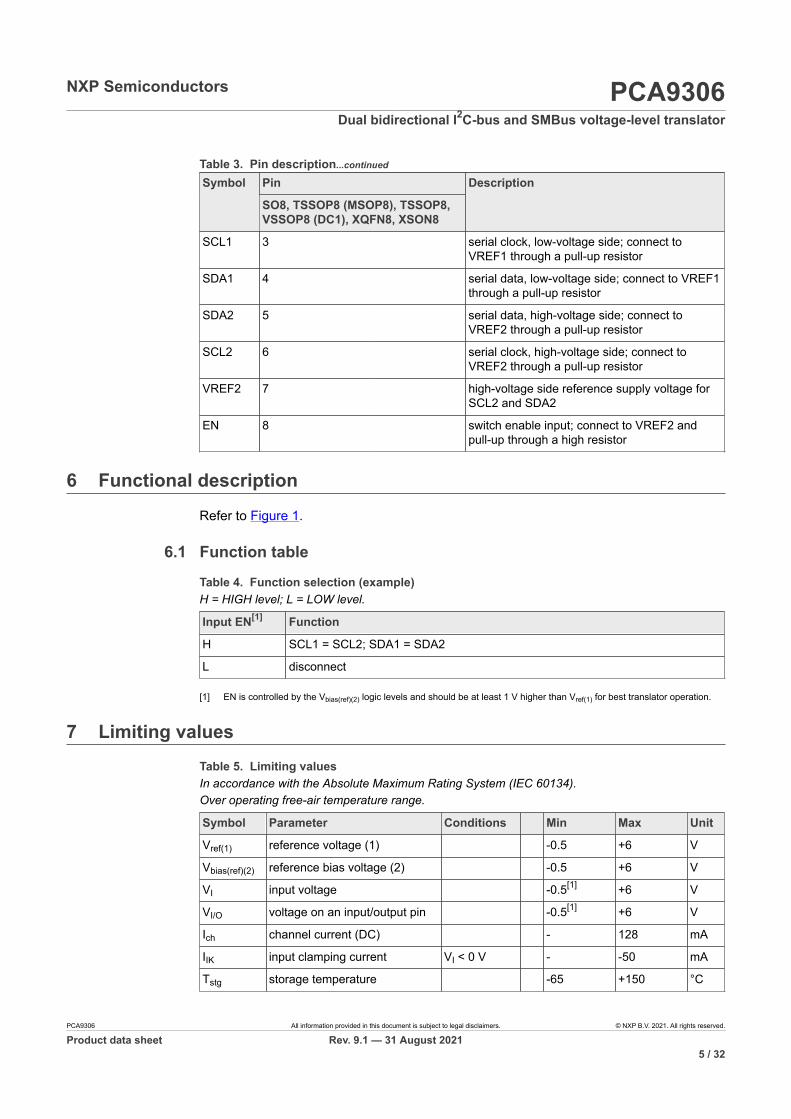
5.2 Pin description
PinSymbol
SO8, TSSOP8 (MSOP8), TSSOP8,VSSOP8 (DC1), XQFN8, XSON8
Description
GND 1 ground (0 V)
VREF1 2 low-voltage side reference supply voltage forSCL1 and SDA1
Table 3. Pin description
PCA9306 All information provided in this document is subject to legal disclaimers. © NXP B.V. 2021. All rights reserved.
Product data sheet Rev. 9.1 — 31 August 20214 / 32
NXP Semiconductors PCA9306Dual bidirectional I2C-bus and SMBus voltage-level translator
PinSymbol
SO8, TSSOP8 (MSOP8), TSSOP8,VSSOP8 (DC1), XQFN8, XSON8
Description
SCL1 3 serial clock, low-voltage side; connect toVREF1 through a pull-up resistor
SDA1 4 serial data, low-voltage side; connect to VREF1through a pull-up resistor
SDA2 5 serial data, high-voltage side; connect toVREF2 through a pull-up resistor
SCL2 6 serial clock, high-voltage side; connect toVREF2 through a pull-up resistor
VREF2 7 high-voltage side reference supply voltage forSCL2 and SDA2
EN 8 switch enable input; connect to VREF2 andpull-up through a high resistor
Table 3. Pin description...continued
6 Functional description
Refer to Figure 1.
6.1 Function table
H = HIGH level; L = LOW level.
Input EN[1] Function
H SCL1 = SCL2; SDA1 = SDA2
L disconnect
Table 4. Function selection (example)
[1] EN is controlled by the Vbias(ref)(2) logic levels and should be at least 1 V higher than Vref(1) for best translator operation.
7 Limiting values
In accordance with the Absolute Maximum Rating System (IEC 60134).Over operating free-air temperature range.
Symbol Parameter Conditions Min Max Unit
Vref(1) reference voltage (1) -0.5 +6 V
Vbias(ref)(2) reference bias voltage (2) -0.5 +6 V
VI input voltage -0.5[1] +6 V
VI/O voltage on an input/output pin -0.5[1] +6 V
Ich channel current (DC) - 128 mA
IIK input clamping current VI < 0 V - -50 mA
Tstg storage temperature -65 +150 °C
Table 5. Limiting values
PCA9306 All information provided in this document is subject to legal disclaimers. © NXP B.V. 2021. All rights reserved.
Product data sheet Rev. 9.1 — 31 August 20215 / 32
NXP Semiconductors PCA9306Dual bidirectional I2C-bus and SMBus voltage-level translator
[1] The input and input/output negative voltage ratings may be exceeded if the input and input/output clamp current ratingsare observed.
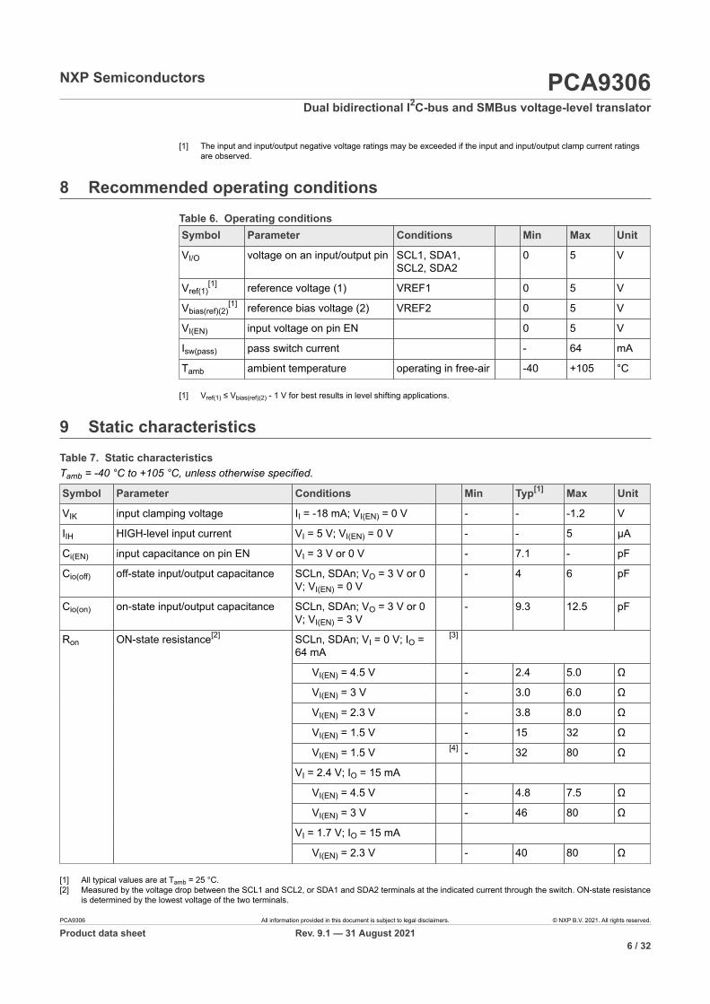
8 Recommended operating conditions
Symbol Parameter Conditions Min Max Unit
VI/O voltage on an input/output pin SCL1, SDA1,SCL2, SDA2
0 5 V
Vref(1)[1] reference voltage (1) VREF1 0 5 V
Vbias(ref)(2)[1] reference bias voltage (2) VREF2 0 5 V
VI(EN) input voltage on pin EN 0 5 V
Isw(pass) pass switch current - 64 mA
Tamb ambient temperature operating in free-air -40 +105 °C
Table 6. Operating conditions
[1] Vref(1) ≤ Vbias(ref)(2) - 1 V for best results in level shifting applications.
9 Static characteristics
Tamb = -40 °C to +105 °C, unless otherwise specified.
Symbol Parameter Conditions Min Typ[1] Max Unit
VIK input clamping voltage II = -18 mA; VI(EN) = 0 V - - -1.2 V
IIH HIGH-level input current VI = 5 V; VI(EN) = 0 V - - 5 μA
Ci(EN) input capacitance on pin EN VI = 3 V or 0 V - 7.1 - pF
Cio(off) off-state input/output capacitance SCLn, SDAn; VO = 3 V or 0V; VI(EN) = 0 V
- 4 6 pF
Cio(on) on-state input/output capacitance SCLn, SDAn; VO = 3 V or 0V; VI(EN) = 3 V
- 9.3 12.5 pF
SCLn, SDAn; VI = 0 V; IO =64 mA
[3]
VI(EN) = 4.5 V - 2.4 5.0 Ω
VI(EN) = 3 V - 3.0 6.0 Ω
VI(EN) = 2.3 V - 3.8 8.0 Ω
VI(EN) = 1.5 V - 15 32 Ω
VI(EN) = 1.5 V [4] - 32 80 Ω
VI = 2.4 V; IO = 15 mA
VI(EN) = 4.5 V - 4.8 7.5 Ω
VI(EN) = 3 V - 46 80 Ω
VI = 1.7 V; IO = 15 mA
Ron ON-state resistance[2]
VI(EN) = 2.3 V - 40 80 Ω
Table 7. Static characteristics
[1] All typical values are at Tamb = 25 °C.[2] Measured by the voltage drop between the SCL1 and SCL2, or SDA1 and SDA2 terminals at the indicated current through the switch. ON-state resistance
is determined by the lowest voltage of the two terminals.
PCA9306 All information provided in this document is subject to legal disclaimers. © NXP B.V. 2021. All rights reserved.
Product data sheet Rev. 9.1 — 31 August 20216 / 32
NXP Semiconductors PCA9306Dual bidirectional I2C-bus and SMBus voltage-level translator
[3] Guaranteed by design.[4] For DC, DC1 (VSSOP8) and GD1 (XSON8U) packages only.
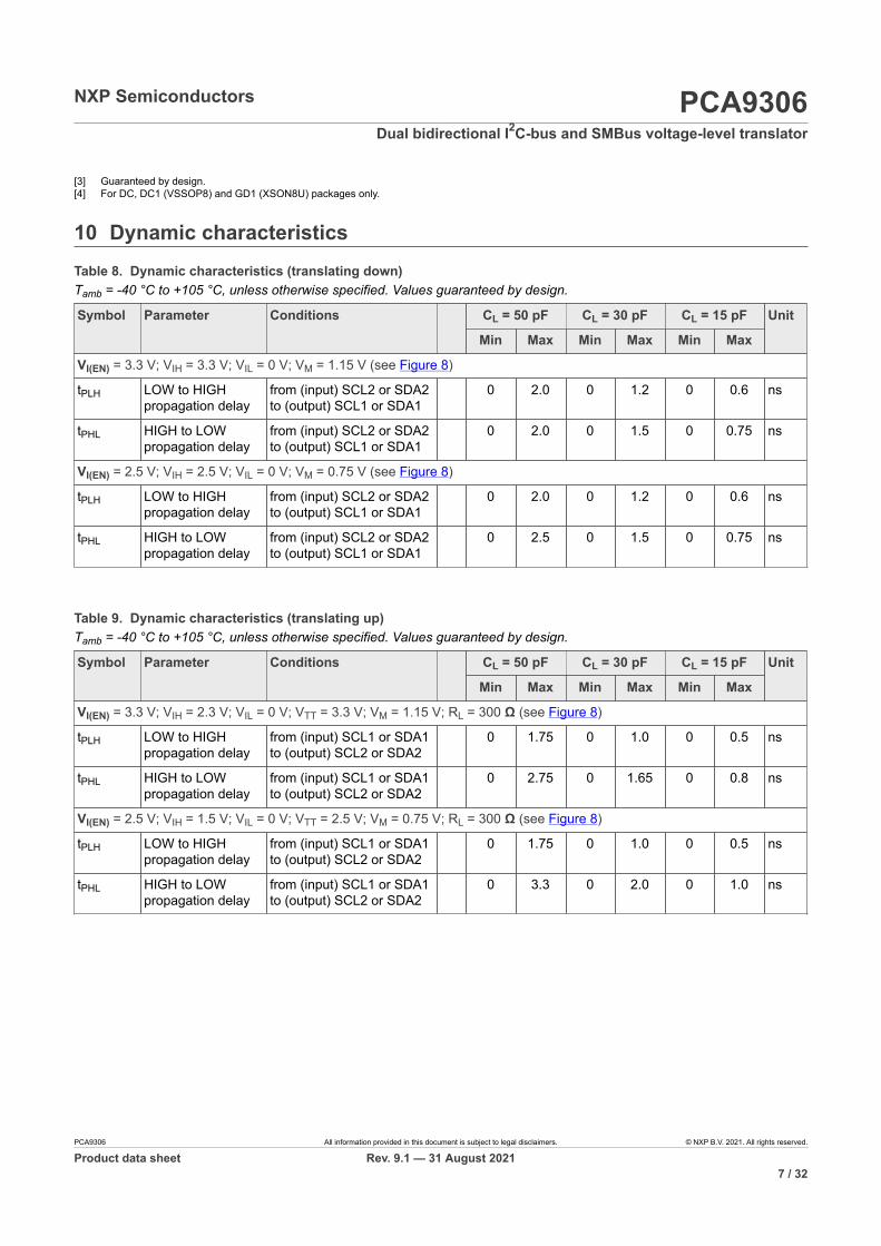
10 Dynamic characteristics
Tamb = -40 °C to +105 °C, unless otherwise specified. Values guaranteed by design.
CL = 50 pF CL = 30 pF CL = 15 pFSymbol Parameter Conditions
Min Max Min Max Min Max
Unit
VI(EN) = 3.3 V; VIH = 3.3 V; VIL = 0 V; VM = 1.15 V (see Figure 8)
tPLH LOW to HIGHpropagation delay
from (input) SCL2 or SDA2to (output) SCL1 or SDA1
0 2.0 0 1.2 0 0.6 ns
tPHL HIGH to LOWpropagation delay
from (input) SCL2 or SDA2to (output) SCL1 or SDA1
0 2.0 0 1.5 0 0.75 ns
VI(EN) = 2.5 V; VIH = 2.5 V; VIL = 0 V; VM = 0.75 V (see Figure 8)
tPLH LOW to HIGHpropagation delay
from (input) SCL2 or SDA2to (output) SCL1 or SDA1
0 2.0 0 1.2 0 0.6 ns
tPHL HIGH to LOWpropagation delay
from (input) SCL2 or SDA2to (output) SCL1 or SDA1
0 2.5 0 1.5 0 0.75 ns
Table 8. Dynamic characteristics (translating down)
Tamb = -40 °C to +105 °C, unless otherwise specified. Values guaranteed by design.
CL = 50 pF CL = 30 pF CL = 15 pFSymbol Parameter Conditions
Min Max Min Max Min Max
Unit
VI(EN) = 3.3 V; VIH = 2.3 V; VIL = 0 V; VTT = 3.3 V; VM = 1.15 V; RL = 300 Ω (see Figure 8)
tPLH LOW to HIGHpropagation delay
from (input) SCL1 or SDA1to (output) SCL2 or SDA2
0 1.75 0 1.0 0 0.5 ns
tPHL HIGH to LOWpropagation delay
from (input) SCL1 or SDA1to (output) SCL2 or SDA2
0 2.75 0 1.65 0 0.8 ns
VI(EN) = 2.5 V; VIH = 1.5 V; VIL = 0 V; VTT = 2.5 V; VM = 0.75 V; RL = 300 Ω (see Figure 8)
tPLH LOW to HIGHpropagation delay
from (input) SCL1 or SDA1to (output) SCL2 or SDA2
0 1.75 0 1.0 0 0.5 ns
tPHL HIGH to LOWpropagation delay
from (input) SCL1 or SDA1to (output) SCL2 or SDA2
0 3.3 0 2.0 0 1.0 ns
Table 9. Dynamic characteristics (translating up)
PCA9306 All information provided in this document is subject to legal disclaimers. © NXP B.V. 2021. All rights reserved.
Product data sheet Rev. 9.1 — 31 August 20217 / 32
NXP Semiconductors PCA9306Dual bidirectional I2C-bus and SMBus voltage-level translator
002aab845
VTT
RL
S1S2 (open)
CL
from output under test
a. Load circuit002aab846
VIH
VIL
VM VMinput
output
VOH
VOL
VM VM
b. Timing diagram
S1 = translating up; S2 = translating down.CL includes probe and jig capacitance.All input pulses are supplied by generators having the following characteristics: PRR ≤ 10 MHz; Zo = 50 Ω; tr ≤ 2 ns; tf ≤ 2ns.The outputs are measured one at a time, with one transition per measurement.Figure 8. Load circuit for outputs
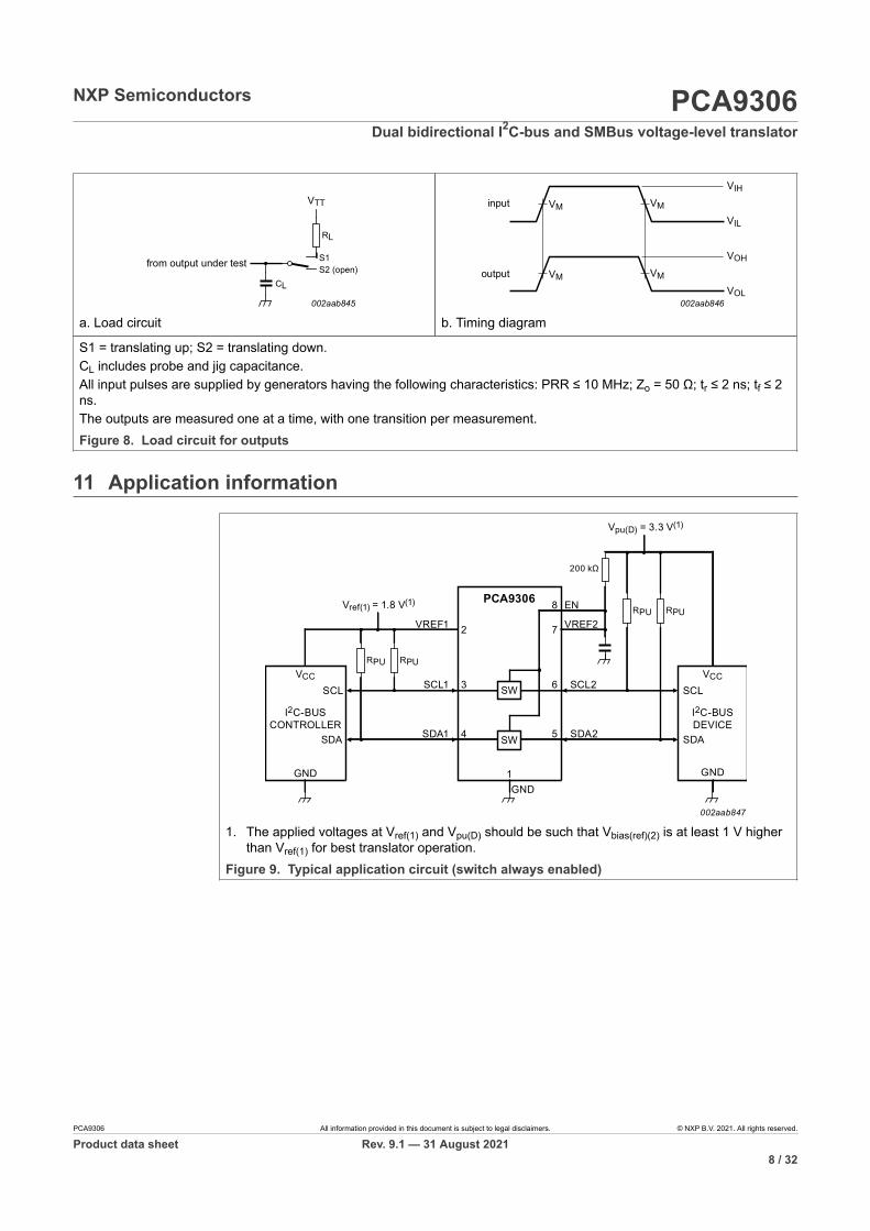
11 Application information
002aab847
SCL1
SDA1
VREF1
GND
3
4
VREF2
1
6
5
SCL2
SDA2
8 EN
SW
SW
PCA9306
7
200 kΩ
RPU RPU
Vpu(D) = 3.3 V(1)
I2C-BUSDEVICE
SCL
SDA
VCC
GND
2
= 1.8 V(1)Vref(1)
RPU RPU
I2C-BUSCONTROLLER
SCL
SDA
VCC
GND
1. The applied voltages at Vref(1) and Vpu(D) should be such that Vbias(ref)(2) is at least 1 V higherthan Vref(1) for best translator operation.
Figure 9. Typical application circuit (switch always enabled)
PCA9306 All information provided in this document is subject to legal disclaimers. © NXP B.V. 2021. All rights reserved.
Product data sheet Rev. 9.1 — 31 August 20218 / 32
NXP Semiconductors PCA9306Dual bidirectional I2C-bus and SMBus voltage-level translator
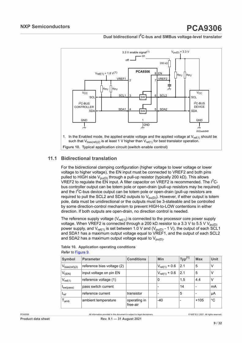
002aab848
SCL1
SDA1
VREF1
GND
3
4
VREF2
1
6
5
SCL2
SDA2
8 EN
SW
SW
PCA9306
7
200 k
RPU RPU
Vpu(D) = 3.3 V
I2C-BUSDEVICE
SCL
SDA
VCC
GND
2
Vref(1) = 1.8 V(1)
RPU RPU
SCL
SDA
VCC
GND
onoff
3.3 V enable signal(1)
I2C-BUSCONTROLLER
1. In the Enabled mode, the applied enable voltage and the applied voltage at Vref(1) should besuch that Vbias(ref)(2) is at least 1 V higher than Vref(1) for best translator operation.
Figure 10. Typical application circuit (switch enable control)
11.1 Bidirectional translationFor the bidirectional clamping configuration (higher voltage to lower voltage or lowervoltage to higher voltage), the EN input must be connected to VREF2 and both pinspulled to HIGH side Vpu(D) through a pull-up resistor (typically 200 kΩ). This allowsVREF2 to regulate the EN input. A filter capacitor on VREF2 is recommended. The I2C-bus controller output can be totem pole or open-drain (pull-up resistors may be required)and the I2C-bus device output can be totem pole or open-drain (pull-up resistors arerequired to pull the SCL2 and SDA2 outputs to Vpu(D)). However, if either output is totempole, data must be unidirectional or the outputs must be 3-stateable and be controlledby some direction-control mechanism to prevent HIGH-to-LOW contentions in eitherdirection. If both outputs are open-drain, no direction control is needed.
The reference supply voltage (Vref(1)) is connected to the processor core power supplyvoltage. When VREF2 is connected through a 200 kΩ resistor to a 3.3 V to 5.5 V Vpu(D)power supply, and Vref(1) is set between 1.0 V and (Vpu(D) - 1 V), the output of each SCL1and SDA1 has a maximum output voltage equal to VREF1, and the output of each SCL2and SDA2 has a maximum output voltage equal to Vpu(D).
Refer to Figure 9.
Symbol Parameter Conditions Min Typ[1] Max Unit
Vbias(ref)(2) reference bias voltage (2) Vref(1) + 0.6 2.1 5 V
VI(EN) input voltage on pin EN Vref(1) + 0.6 2.1 5 V
Vref(1) reference voltage (1) 0 1.5 4.4 V
Isw(pass) pass switch current - 14 - mA
Iref reference current transistor - 5 - μA
Tamb ambient temperature operating infree-air
-40 - +105 °C
Table 10. Application operating conditions
PCA9306 All information provided in this document is subject to legal disclaimers. © NXP B.V. 2021. All rights reserved.
Product data sheet Rev. 9.1 — 31 August 20219 / 32
NXP Semiconductors PCA9306Dual bidirectional I2C-bus and SMBus voltage-level translator
[1] All typical values are at Tamb = 25 °C.
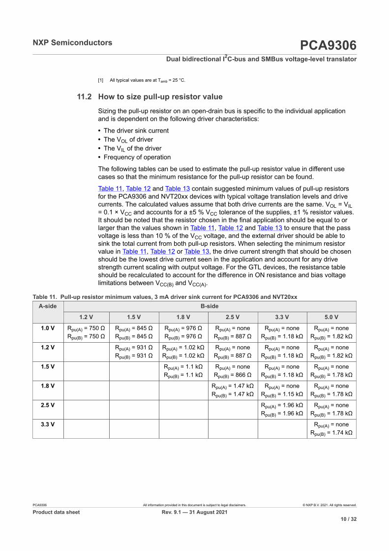
11.2 How to size pull-up resistor valueSizing the pull-up resistor on an open-drain bus is specific to the individual applicationand is dependent on the following driver characteristics:
• The driver sink current• The VOL of driver• The VIL of the driver• Frequency of operation
The following tables can be used to estimate the pull-up resistor value in different usecases so that the minimum resistance for the pull-up resistor can be found.
Table 11, Table 12 and Table 13 contain suggested minimum values of pull-up resistorsfor the PCA9306 and NVT20xx devices with typical voltage translation levels and drivecurrents. The calculated values assume that both drive currents are the same. VOL = VIL= 0.1 × VCC and accounts for a ±5 % VCC tolerance of the supplies, ±1 % resistor values.It should be noted that the resistor chosen in the final application should be equal to orlarger than the values shown in Table 11, Table 12 and Table 13 to ensure that the passvoltage is less than 10 % of the VCC voltage, and the external driver should be able tosink the total current from both pull-up resistors. When selecting the minimum resistorvalue in Table 11, Table 12 or Table 13, the drive current strength that should be chosenshould be the lowest drive current seen in the application and account for any drivestrength current scaling with output voltage. For the GTL devices, the resistance tableshould be recalculated to account for the difference in ON resistance and bias voltagelimitations between VCC(B) and VCC(A).
B-sideA-side
1.2 V 1.5 V 1.8 V 2.5 V 3.3 V 5.0 V
1.0 V Rpu(A) = 750 ΩRpu(B) = 750 Ω
Rpu(A) = 845 ΩRpu(B) = 845 Ω
Rpu(A) = 976 ΩRpu(B) = 976 Ω
Rpu(A) = noneRpu(B) = 887 Ω
Rpu(A) = noneRpu(B) = 1.18 kΩ
Rpu(A) = noneRpu(B) = 1.82 kΩ
1.2 V Rpu(A) = 931 ΩRpu(B) = 931 Ω
Rpu(A) = 1.02 kΩRpu(B) = 1.02 kΩ
Rpu(A) = noneRpu(B) = 887 Ω
Rpu(A) = noneRpu(B) = 1.18 kΩ
Rpu(A) = noneRpu(B) = 1.82 kΩ
1.5 V Rpu(A) = 1.1 kΩRpu(B) = 1.1 kΩ
Rpu(A) = noneRpu(B) = 866 Ω
Rpu(A) = noneRpu(B) = 1.18 kΩ
Rpu(A) = noneRpu(B) = 1.78 kΩ
1.8 V Rpu(A) = 1.47 kΩRpu(B) = 1.47 kΩ
Rpu(A) = noneRpu(B) = 1.15 kΩ
Rpu(A) = noneRpu(B) = 1.78 kΩ
2.5 V Rpu(A) = 1.96 kΩRpu(B) = 1.96 kΩ
Rpu(A) = noneRpu(B) = 1.78 kΩ
3.3 V Rpu(A) = noneRpu(B) = 1.74 kΩ
Table 11. Pull-up resistor minimum values, 3 mA driver sink current for PCA9306 and NVT20xx
PCA9306 All information provided in this document is subject to legal disclaimers. © NXP B.V. 2021. All rights reserved.
Product data sheet Rev. 9.1 — 31 August 202110 / 32
NXP Semiconductors PCA9306Dual bidirectional I2C-bus and SMBus voltage-level translator
B-sideA-side
1.2 V 1.5 V 1.8 V 2.5 V 3.3 V 5.0 V
1.0 V Rpu(A) = 221 ΩRpu(B) = 221 Ω
Rpu(A) = 255 ΩRpu(B) = 255 Ω
Rpu(A) = 287 ΩRpu(B) = 287 Ω
Rpu(A) = noneRpu(B) = 267 Ω
Rpu(A) = noneRpu(B) = 357 Ω
Rpu(A) = noneRpu(B) = 549 Ω
1.2 V Rpu(A) = 274 ΩRpu(B) = 274 Ω
Rpu(A) = 309 ΩRpu(B) = 309 Ω
Rpu(A) = noneRpu(B) = 267 Ω
Rpu(A) = noneRpu(B) = 357 Ω
Rpu(A) = noneRpu(B) = 549 Ω
1.5 V Rpu(A) = 332 ΩRpu(B) = 332 Ω
Rpu(A) = noneRpu(B) = 261 Ω
Rpu(A) = noneRpu(B) = 348 Ω
Rpu(A) = noneRpu(B) = 536 Ω
1.8 V Rpu(A) = 442 ΩRpu(B) = 442 Ω
Rpu(A) = noneRpu(B) = 348 Ω
Rpu(A) = noneRpu(B) = 536 Ω
2.5 V Rpu(A) = 590 ΩRpu(B) = 590 Ω
Rpu(A) = noneRpu(B) = 523 Ω
3.3 V Rpu(A) = noneRpu(B) = 523 Ω
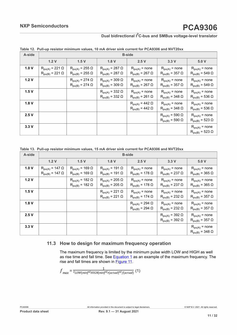
Table 12. Pull-up resistor minimum values, 10 mA driver sink current for PCA9306 and NVT20xx
B-sideA-side
1.2 V 1.5 V 1.8 V 2.5 V 3.3 V 5.0 V
1.0 V Rpu(A) = 147 ΩRpu(B) = 147 Ω
Rpu(A) = 169 ΩRpu(B) = 169 Ω
Rpu(A) = 191 ΩRpu(B) = 191 Ω
Rpu(A) = noneRpu(B) = 178 Ω
Rpu(A) = noneRpu(B) = 237 Ω
Rpu(A) = noneRpu(B) = 365 Ω
1.2 V Rpu(A) = 182 ΩRpu(B) = 182 Ω
Rpu(A) = 205 ΩRpu(B) = 205 Ω
Rpu(A) = noneRpu(B) = 178 Ω
Rpu(A) = noneRpu(B) = 237 Ω
Rpu(A) = noneRpu(B) = 365 Ω
1.5 V Rpu(A) = 221 ΩRpu(B) = 221 Ω
Rpu(A) = noneRpu(B) = 174 Ω
Rpu(A) = noneRpu(B) = 232 Ω
Rpu(A) = noneRpu(B) = 357 Ω
1.8 V Rpu(A) = 294 ΩRpu(B) = 294 Ω
Rpu(A) = noneRpu(B) = 232 Ω
Rpu(A) = noneRpu(B) = 357 Ω
2.5 V Rpu(A) = 392 ΩRpu(B) = 392 Ω
Rpu(A) = noneRpu(B) = 357 Ω
3.3 V Rpu(A) = noneRpu(B) = 348 Ω
Table 13. Pull-up resistor minimum values, 15 mA driver sink current for PCA9306 and NVT20xx
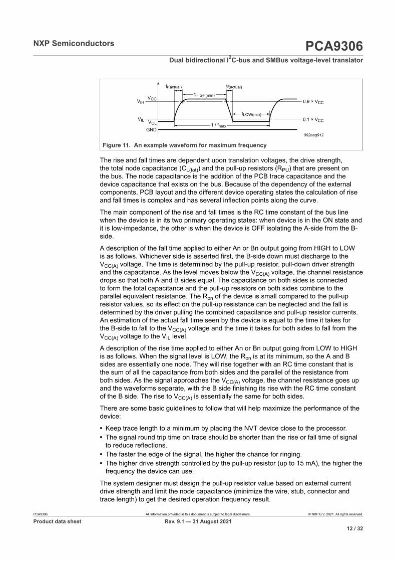
11.3 How to design for maximum frequency operationThe maximum frequency is limited by the minimum pulse width LOW and HIGH as wellas rise time and fall time. See Equation 1 as an example of the maximum frequency. Therise and fall times are shown in Figure 11.
(1)
PCA9306 All information provided in this document is subject to legal disclaimers. © NXP B.V. 2021. All rights reserved.
Product data sheet Rev. 9.1 — 31 August 202111 / 32
NXP Semiconductors PCA9306Dual bidirectional I2C-bus and SMBus voltage-level translator
002aag912
tr(actual) tf(actual)
GNDVOL
VIL
VIHVCC
tHIGH(min)
tLOW(min)
1 / fmax
0.9 × VCC
0.1 × VCC
Figure 11. An example waveform for maximum frequency
The rise and fall times are dependent upon translation voltages, the drive strength,the total node capacitance (CL(tot)) and the pull-up resistors (RPU) that are present onthe bus. The node capacitance is the addition of the PCB trace capacitance and thedevice capacitance that exists on the bus. Because of the dependency of the externalcomponents, PCB layout and the different device operating states the calculation of riseand fall times is complex and has several inflection points along the curve.
The main component of the rise and fall times is the RC time constant of the bus linewhen the device is in its two primary operating states: when device is in the ON state andit is low-impedance, the other is when the device is OFF isolating the A-side from the B-side.
A description of the fall time applied to either An or Bn output going from HIGH to LOWis as follows. Whichever side is asserted first, the B-side down must discharge to theVCC(A) voltage. The time is determined by the pull-up resistor, pull-down driver strengthand the capacitance. As the level moves below the VCC(A) voltage, the channel resistancedrops so that both A and B sides equal. The capacitance on both sides is connectedto form the total capacitance and the pull-up resistors on both sides combine to theparallel equivalent resistance. The Ron of the device is small compared to the pull-upresistor values, so its effect on the pull-up resistance can be neglected and the fall isdetermined by the driver pulling the combined capacitance and pull-up resistor currents.An estimation of the actual fall time seen by the device is equal to the time it takes forthe B-side to fall to the VCC(A) voltage and the time it takes for both sides to fall from theVCC(A) voltage to the VIL level.
A description of the rise time applied to either An or Bn output going from LOW to HIGHis as follows. When the signal level is LOW, the Ron is at its minimum, so the A and Bsides are essentially one node. They will rise together with an RC time constant that isthe sum of all the capacitance from both sides and the parallel of the resistance fromboth sides. As the signal approaches the VCC(A) voltage, the channel resistance goes upand the waveforms separate, with the B side finishing its rise with the RC time constantof the B side. The rise to VCC(A) is essentially the same for both sides.
There are some basic guidelines to follow that will help maximize the performance of thedevice:
• Keep trace length to a minimum by placing the NVT device close to the processor.• The signal round trip time on trace should be shorter than the rise or fall time of signal
to reduce reflections.• The faster the edge of the signal, the higher the chance for ringing.• The higher drive strength controlled by the pull-up resistor (up to 15 mA), the higher the
frequency the device can use.
The system designer must design the pull-up resistor value based on external currentdrive strength and limit the node capacitance (minimize the wire, stub, connector andtrace length) to get the desired operation frequency result.
PCA9306 All information provided in this document is subject to legal disclaimers. © NXP B.V. 2021. All rights reserved.
Product data sheet Rev. 9.1 — 31 August 202112 / 32
NXP Semiconductors PCA9306Dual bidirectional I2C-bus and SMBus voltage-level translator
12 Package outline
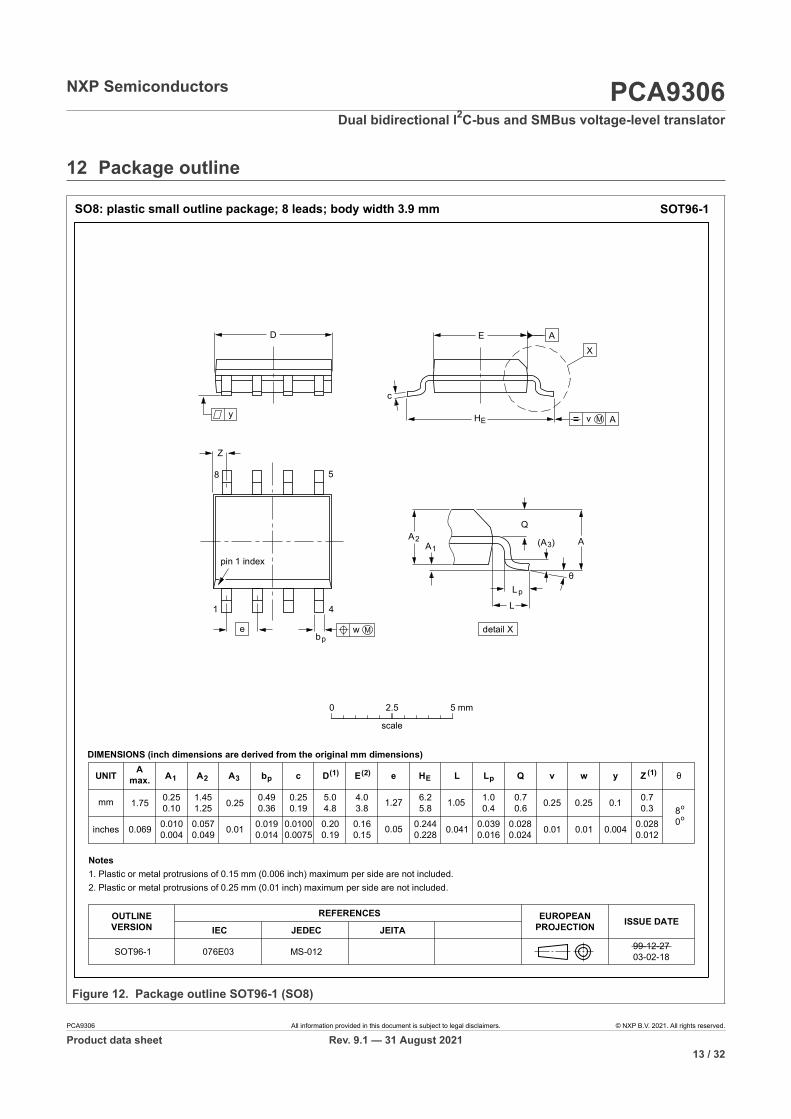
UNIT A max. A 1 A 2 A 3 b p c D (1) E (2) (1) e H E L L p Q Z y w v θ
REFERENCES OUTLINE VERSION
EUROPEAN PROJECTION ISSUE DATE
IEC JEDEC JEITA
mm
inches
1.75 0.25 0.10
1.45 1.25 0.25 0.49
0.36 0.25 0.19
5.0 4.8
4.0 3.8 1.27 6.2
5.8 1.05 0.7 0.6
0.7 0.3 8
0
o o
0.25 0.1 0.25
DIMENSIONS (inch dimensions are derived from the original mm dimensions)
Notes 1. Plastic or metal protrusions of 0.15 mm (0.006 inch) maximum per side are not included. 2. Plastic or metal protrusions of 0.25 mm (0.01 inch) maximum per side are not included.
1.0 0.4
SOT96-1
X
w M
θ
A A 1 A 2
b p
D
H E
L p
Q
detail X
E
Z
e
c
L
v M A
(A ) 3
A
4
5
pin 1 index
1
8
y
076E03 MS-012
0.069 0.010 0.004
0.057 0.049 0.01 0.019
0.014 0.0100 0.0075
0.20 0.19
0.16 0.15 0.05 0.244
0.228 0.028 0.024
0.028 0.012 0.01 0.01 0.041 0.004 0.039
0.016
0 2.5 5 mm
scale
SO8: plastic small outline package; 8 leads; body width 3.9 mm SOT96-1
99-12-27 03-02-18
Figure 12. Package outline SOT96-1 (SO8)
PCA9306 All information provided in this document is subject to legal disclaimers. © NXP B.V. 2021. All rights reserved.
Product data sheet Rev. 9.1 — 31 August 202113 / 32
NXP Semiconductors PCA9306Dual bidirectional I2C-bus and SMBus voltage-level translator
UNIT A1 A
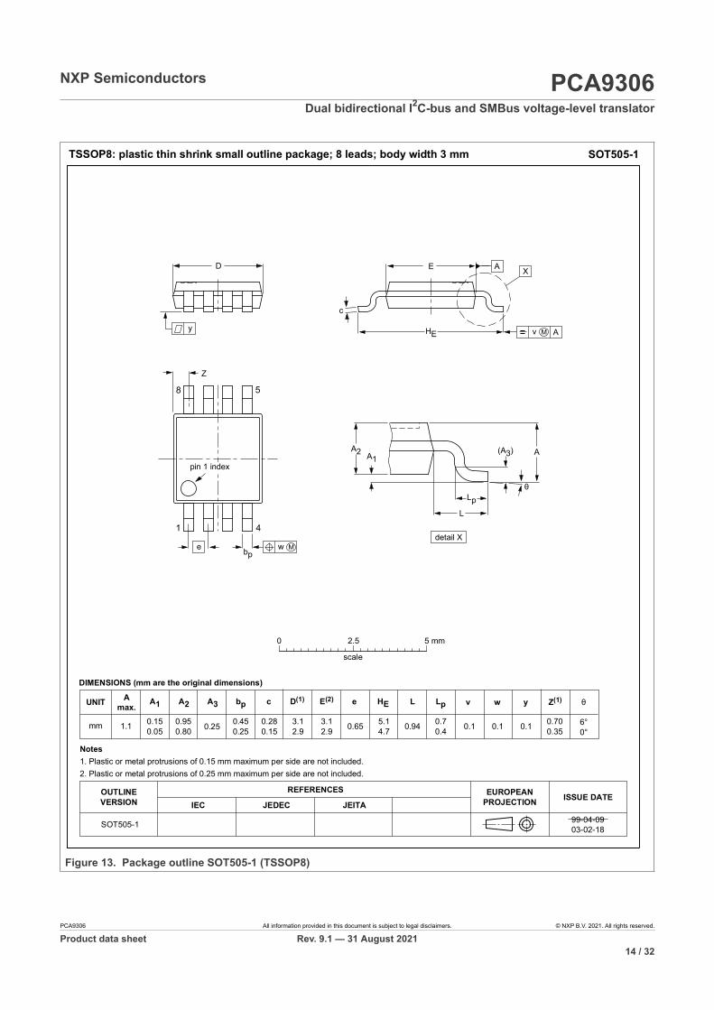
max. A2 A3 bp L HE Lp w y v c e D(1) E(2) Z(1) θ
REFERENCES OUTLINE VERSION
EUROPEAN PROJECTION ISSUE DATE
IEC JEDEC JEITA
mm 0.15 0.05
0.95 0.80
0.45 0.25
0.28 0.15
3.1 2.9
3.1 2.9 0.65 5.1
4.7 0.70 0.35
6° 0°
0.1 0.1 0.1 0.94
DIMENSIONS (mm are the original dimensions)
Notes 1. Plastic or metal protrusions of 0.15 mm maximum per side are not included. 2. Plastic or metal protrusions of 0.25 mm maximum per side are not included.
0.7 0.4
SOT505-1 99-04-09 03-02-18
w M bp
D
Z
e
0.25
1 4
8 5
θ
A A2 A1
Lp
(A3)
detail X
L
HE
E
c
v M A
X A
y
2.5 5 mm 0
scale
TSSOP8: plastic thin shrink small outline package; 8 leads; body width 3 mm SOT505-1
1.1
pin 1 index
Figure 13. Package outline SOT505-1 (TSSOP8)
PCA9306 All information provided in this document is subject to legal disclaimers. © NXP B.V. 2021. All rights reserved.
Product data sheet Rev. 9.1 — 31 August 202114 / 32
NXP Semiconductors PCA9306Dual bidirectional I2C-bus and SMBus voltage-level translator
UNIT A1 A
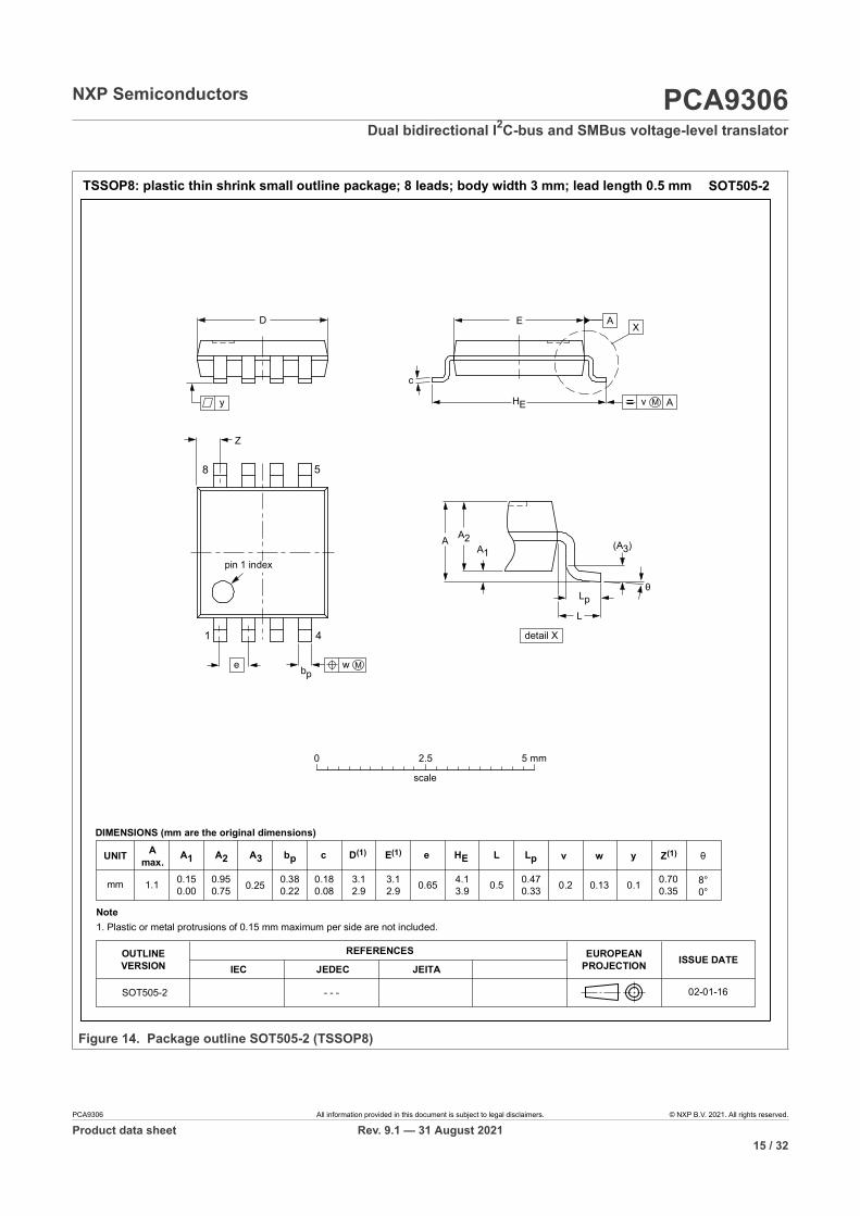
max. A2 A3 bp L HE Lp w y v c e D(1) E(1) Z(1) θ
REFERENCES OUTLINE VERSION
EUROPEAN PROJECTION ISSUE DATE
IEC JEDEC JEITA
mm 0.15 0.00
0.95 0.75
0.38 0.22
0.18 0.08
3.1 2.9
3.1 2.9 0.65 4.1
3.9 0.70 0.35
8° 0°
0.13 0.1 0.2 0.5
DIMENSIONS (mm are the original dimensions)
Note 1. Plastic or metal protrusions of 0.15 mm maximum per side are not included.
0.47 0.33
SOT505-2 - - - 02-01-16
w M bp
D
Z
e
0.25
1 4
8 5
θ
A2 A1
Lp
(A3)
detail X
A
L
HE
E
c
v M A
X A
y
2.5 5 mm 0
scale
TSSOP8: plastic thin shrink small outline package; 8 leads; body width 3 mm; lead length 0.5 mm SOT505-2
1.1
pin 1 index
Figure 14. Package outline SOT505-2 (TSSOP8)
PCA9306 All information provided in this document is subject to legal disclaimers. © NXP B.V. 2021. All rights reserved.
Product data sheet Rev. 9.1 — 31 August 202115 / 32
NXP Semiconductors PCA9306Dual bidirectional I2C-bus and SMBus voltage-level translator
ReferencesOutlineversion
Europeanprojection Issue date
IEC JEDEC JEITA
SOT765-1 MO-187
sot765-1_po
07-06-0216-05-31
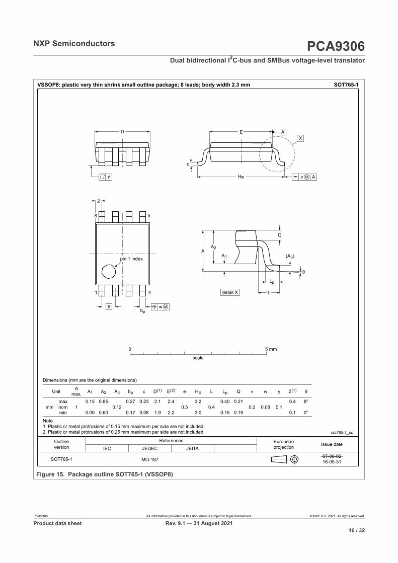
Unit
mmmaxnommin
0.15 0.27 0.23 2.10.5
0.4
Amax.
Dimensions (mm are the original dimensions)
Note1. Plastic or metal protrusions of 0.15 mm maximum per side are not included.2. Plastic or metal protrusions of 0.25 mm maximum per side are not included.
VSSOP8: plastic very thin shrink small outline package; 8 leads; body width 2.3 mm SOT765-1
A1 A2
0.85
A3 bp c D(1) E(2) e HE L
0.4
Lp Q v w
1 0.12 0.10.2 0.08
y Z(1)
3.0 0.152.2 0.190.00 0.17 0.08 1.9 0.10.60 0°
3.2 0.402.4 0.21 8°
θ
0
scale
5 mm
detail X
A
y
e
X
v A
bpw
D
Z
1 4
8 5
θ
A2
A1
Q
Lp
(A3)A
L
HE
E
c
pin 1 index
Figure 15. Package outline SOT765-1 (VSSOP8)
PCA9306 All information provided in this document is subject to legal disclaimers. © NXP B.V. 2021. All rights reserved.
Product data sheet Rev. 9.1 — 31 August 202116 / 32
NXP Semiconductors PCA9306Dual bidirectional I2C-bus and SMBus voltage-level translator
ReferencesOutlineversion
Europeanprojection Issue date
IEC JEDEC JEITA
SOT902-2 - - -MO-255- - -
sot902-2_po
16-07-1416-11-08
Unit(1)
mmmaxnommin
0.5 0.05
0.00
1.651.601.55
1.651.601.55
0.55 0.50.150.100.05
0.1 0.05
A
0.2
k
Dimensions
Note1. Plastic or metal protrusions of 0.075 mm maximum per side are not included.
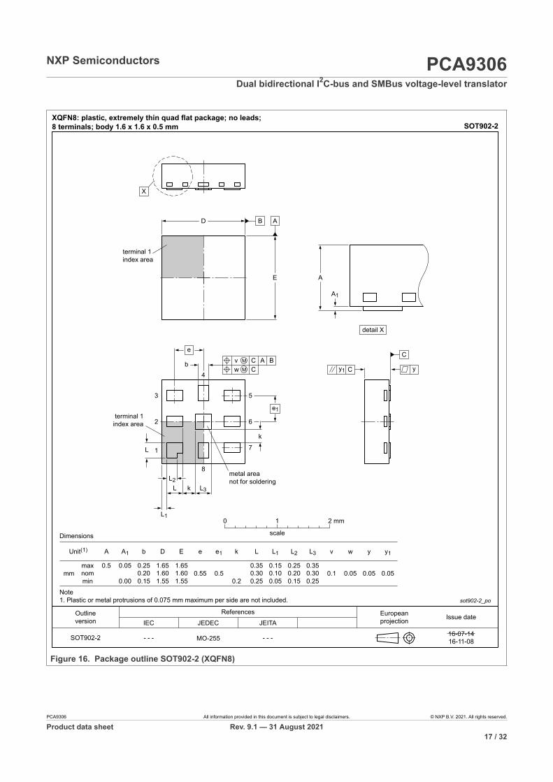
XQFN8: plastic, extremely thin quad flat package; no leads;8 terminals; body 1.6 x 1.6 x 0.5 mm SOT902-2
A1 b
0.250.200.15
D E e e1 L
0.350.300.25
L1
0.250.200.15
L2
0.350.300.25
L3 v w
0.05
y y1
0.05
0 1 2 mm
scale
terminal 1index area
B AD
E
X
C
yCy1
terminal 1index area
3
L k
L1
L2
b
e1
eAC Bv
Cw
2
1
5
6
7
metal areanot for soldering
8
k
4
L
L3
A1
A
detail X
Figure 16. Package outline SOT902-2 (XQFN8)
PCA9306 All information provided in this document is subject to legal disclaimers. © NXP B.V. 2021. All rights reserved.
Product data sheet Rev. 9.1 — 31 August 202117 / 32
NXP Semiconductors PCA9306Dual bidirectional I2C-bus and SMBus voltage-level translator
ReferencesOutline version
European projection Issue date
IEC JEDEC JEITA
SOT1089 MO-252
sot1089_po
10-04-09 10-04-12
Unit
mmmax nom min
0.5 0.04 1.40 1.35 1.30
1.05 1.00 0.95
0.55 0.350.35 0.30 0.27
A(1)
Dimensions
Note 1. Including plating thickness. 2. Visible depending upon used manufacturing technology.
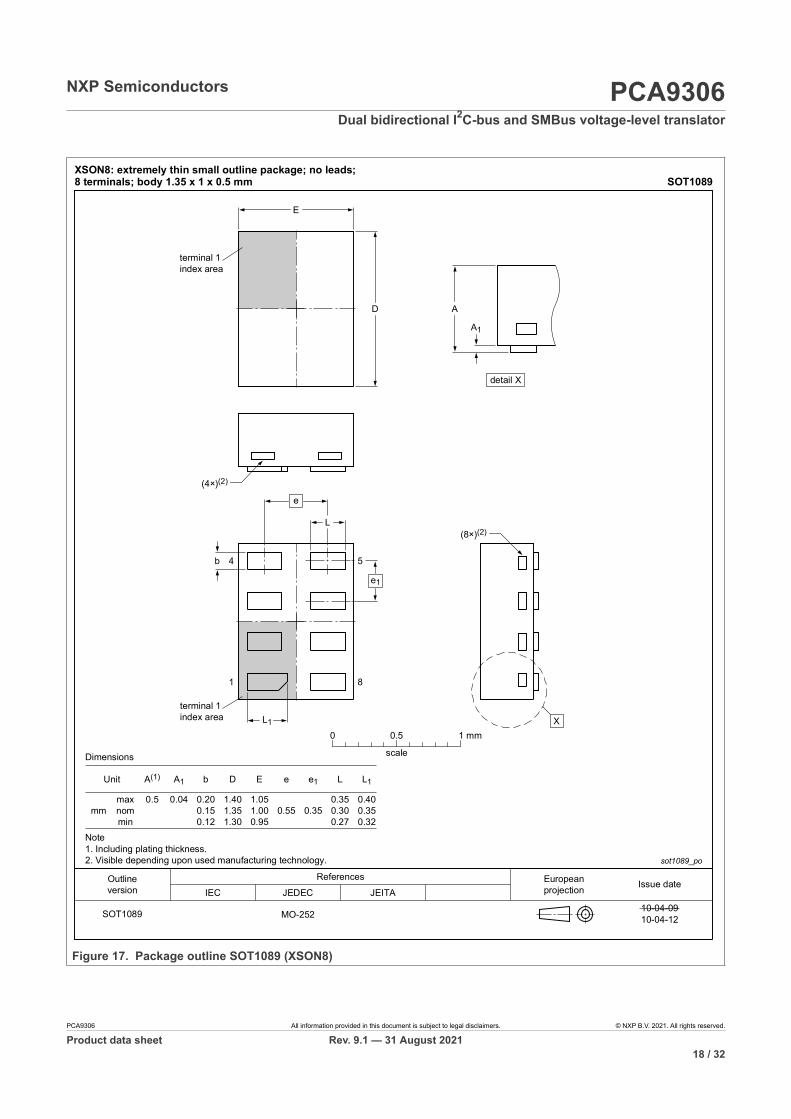
XSON8: extremely thin small outline package; no leads; 8 terminals; body 1.35 x 1 x 0.5 mm SOT1089
A1 b L1
0.40 0.35 0.32
0.20 0.15 0.12
D E e e1 L
0 0.5 1 mm
scale
terminal 1 index area
E
D
detail X
A
A1
L
L1
b
e1
e
terminal 1 index area
1
4
8
5
(4×)(2)
(8×)(2)
X
Figure 17. Package outline SOT1089 (XSON8)
PCA9306 All information provided in this document is subject to legal disclaimers. © NXP B.V. 2021. All rights reserved.
Product data sheet Rev. 9.1 — 31 August 202118 / 32
NXP Semiconductors PCA9306Dual bidirectional I2C-bus and SMBus voltage-level translator
ReferencesOutlineversion
Europeanprojection Issue date
IEC JEDEC JEITA
SOT996-2
sot996-2_po
07-12-2112-11-20
Unit(1)
mmmaxnommin
0.50.05
0.00
2.1
1.9
3.1
2.9
0.5
0.3
0.15
0.05
0.6
0.40.5 1.5 0.05
A
Dimensions (mm are the original dimensions)
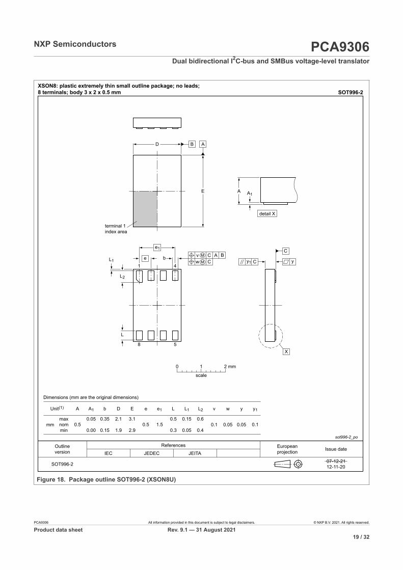
XSON8: plastic extremely thin small outline package; no leads;8 terminals; body 3 x 2 x 0.5 mm SOT996-2
A1 b
0.35
0.15
D E e e1 L L1 L2 v
0.1
w y
0.05
y1
0.1
0 1 2 mm
scale
C
yCy1
X
terminal 1index area
B AD
E
detail X
A A1
b1 4
8 5
e1
e AC BvCw
L2
L1
L
Figure 18. Package outline SOT996-2 (XSON8U)
PCA9306 All information provided in this document is subject to legal disclaimers. © NXP B.V. 2021. All rights reserved.
Product data sheet Rev. 9.1 — 31 August 202119 / 32
NXP Semiconductors PCA9306Dual bidirectional I2C-bus and SMBus voltage-level translator
13 Soldering of SMD packages
This text provides a very brief insight into a complex technology. A more in-depth accountof soldering ICs can be found in Application Note AN10365 “Surface mount reflowsoldering description”.
13.1 Introduction to solderingSoldering is one of the most common methods through which packages are attachedto Printed Circuit Boards (PCBs), to form electrical circuits. The soldered joint providesboth the mechanical and the electrical connection. There is no single soldering methodthat is ideal for all IC packages. Wave soldering is often preferred when through-holeand Surface Mount Devices (SMDs) are mixed on one printed wiring board; however, it isnot suitable for fine pitch SMDs. Reflow soldering is ideal for the small pitches and highdensities that come with increased miniaturization.
13.2 Wave and reflow solderingWave soldering is a joining technology in which the joints are made by solder comingfrom a standing wave of liquid solder. The wave soldering process is suitable for thefollowing:
• Through-hole components• Leaded or leadless SMDs, which are glued to the surface of the printed circuit board
Not all SMDs can be wave soldered. Packages with solder balls, and some leadlesspackages which have solder lands underneath the body, cannot be wave soldered. Also,leaded SMDs with leads having a pitch smaller than ~0.6 mm cannot be wave soldered,due to an increased probability of bridging.
The reflow soldering process involves applying solder paste to a board, followed bycomponent placement and exposure to a temperature profile. Leaded packages,packages with solder balls, and leadless packages are all reflow solderable.
Key characteristics in both wave and reflow soldering are:
• Board specifications, including the board finish, solder masks and vias• Package footprints, including solder thieves and orientation• The moisture sensitivity level of the packages• Package placement• Inspection and repair• Lead-free soldering versus SnPb soldering
13.3 Wave solderingKey characteristics in wave soldering are:
• Process issues, such as application of adhesive and flux, clinching of leads, boardtransport, the solder wave parameters, and the time during which components areexposed to the wave
• Solder bath specifications, including temperature and impurities
13.4 Reflow solderingKey characteristics in reflow soldering are:
PCA9306 All information provided in this document is subject to legal disclaimers. © NXP B.V. 2021. All rights reserved.
Product data sheet Rev. 9.1 — 31 August 202120 / 32
NXP Semiconductors PCA9306Dual bidirectional I2C-bus and SMBus voltage-level translator
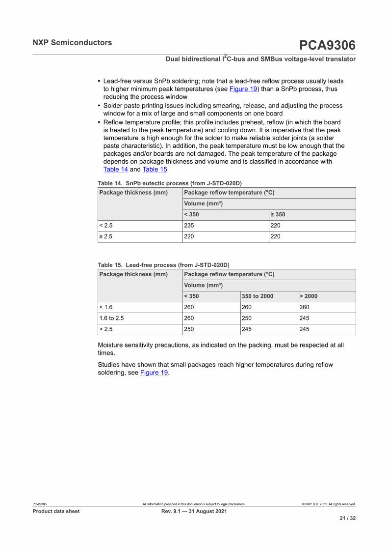
• Lead-free versus SnPb soldering; note that a lead-free reflow process usually leadsto higher minimum peak temperatures (see Figure 19) than a SnPb process, thusreducing the process window
• Solder paste printing issues including smearing, release, and adjusting the processwindow for a mix of large and small components on one board
• Reflow temperature profile; this profile includes preheat, reflow (in which the boardis heated to the peak temperature) and cooling down. It is imperative that the peaktemperature is high enough for the solder to make reliable solder joints (a solderpaste characteristic). In addition, the peak temperature must be low enough that thepackages and/or boards are not damaged. The peak temperature of the packagedepends on package thickness and volume and is classified in accordance withTable 14 and Table 15
Package reflow temperature (°C)
Volume (mm³)
Package thickness (mm)
< 350 ≥ 350
< 2.5 235 220
≥ 2.5 220 220
Table 14. SnPb eutectic process (from J-STD-020D)
Package reflow temperature (°C)
Volume (mm³)
Package thickness (mm)
< 350 350 to 2000 > 2000
< 1.6 260 260 260
1.6 to 2.5 260 250 245
> 2.5 250 245 245
Table 15. Lead-free process (from J-STD-020D)
Moisture sensitivity precautions, as indicated on the packing, must be respected at alltimes.
Studies have shown that small packages reach higher temperatures during reflowsoldering, see Figure 19.
PCA9306 All information provided in this document is subject to legal disclaimers. © NXP B.V. 2021. All rights reserved.
Product data sheet Rev. 9.1 — 31 August 202121 / 32
NXP Semiconductors PCA9306Dual bidirectional I2C-bus and SMBus voltage-level translator
001aac844
temperature
time
minimum peak temperature= minimum soldering temperature
maximum peak temperature= MSL limit, damage level
peak temperature
MSL: Moisture Sensitivity LevelFigure 19. Temperature profiles for large and small components
For further information on temperature profiles, refer to Application Note AN10365“Surface mount reflow soldering description”.
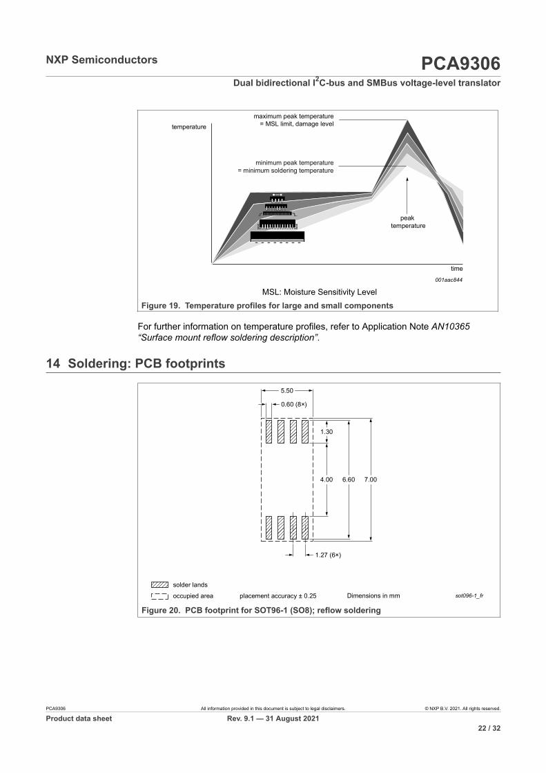
14 Soldering: PCB footprints
sot096-1_froccupied area
solder landsDimensions in mmplacement accuracy ± 0.25
1.30
0.60 (8×)
1.27 (6×)
4.00 6.60
5.50
7.00
Figure 20. PCB footprint for SOT96-1 (SO8); reflow soldering
PCA9306 All information provided in this document is subject to legal disclaimers. © NXP B.V. 2021. All rights reserved.
Product data sheet Rev. 9.1 — 31 August 202122 / 32
NXP Semiconductors PCA9306Dual bidirectional I2C-bus and SMBus voltage-level translator
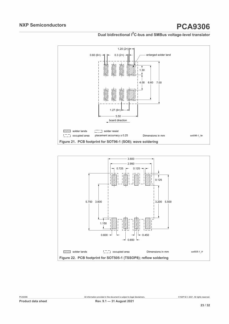
sot096-1_fw
solder resistoccupied areasolder lands
Dimensions in mm
board direction
placement accurracy ± 0.25
4.00
5.50
1.30
0.3 (2×)0.60 (6×)
1.20 (2×)
1.27 (6×)
7.006.60
enlarged solder land
Figure 21. PCB footprint for SOT96-1 (SO8); wave soldering
sot505-1_froccupied areasolder lands Dimensions in mm
3.2003.6005.750
0.725
0.650
0.125
0.4500.600
3.600
2.950
0.125
1.150
5.500
Figure 22. PCB footprint for SOT505-1 (TSSOP8); reflow soldering
PCA9306 All information provided in this document is subject to legal disclaimers. © NXP B.V. 2021. All rights reserved.
Product data sheet Rev. 9.1 — 31 August 202123 / 32
NXP Semiconductors PCA9306Dual bidirectional I2C-bus and SMBus voltage-level translator
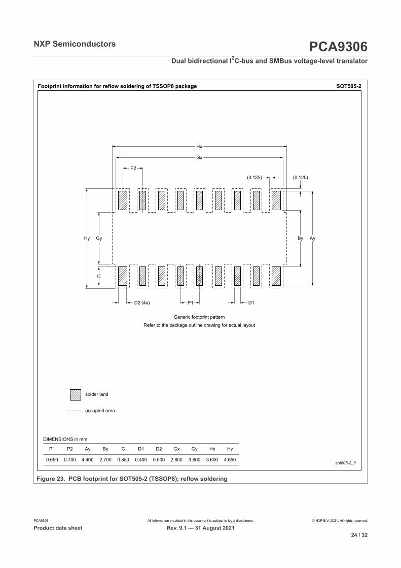
DIMENSIONS in mm
Ay By D1 D2 Gy HyP1 C Gx
sot505-2_fr
Hx
SOT505-2
solder land
occupied area
Footprint information for reflow soldering of TSSOP8 package
AyByGy
C
Hy
Hx
Gx
P1
Generic footprint pattern
Refer to the package outline drawing for actual layout
P2
(0.125) (0.125)
D1D2 (4x)
P2
4.400 2.700 0.850 0.400 0.500 2.800 3.600 4.6503.6000.650 0.700
Figure 23. PCB footprint for SOT505-2 (TSSOP8); reflow soldering
PCA9306 All information provided in this document is subject to legal disclaimers. © NXP B.V. 2021. All rights reserved.
Product data sheet Rev. 9.1 — 31 August 202124 / 32
NXP Semiconductors PCA9306Dual bidirectional I2C-bus and SMBus voltage-level translator
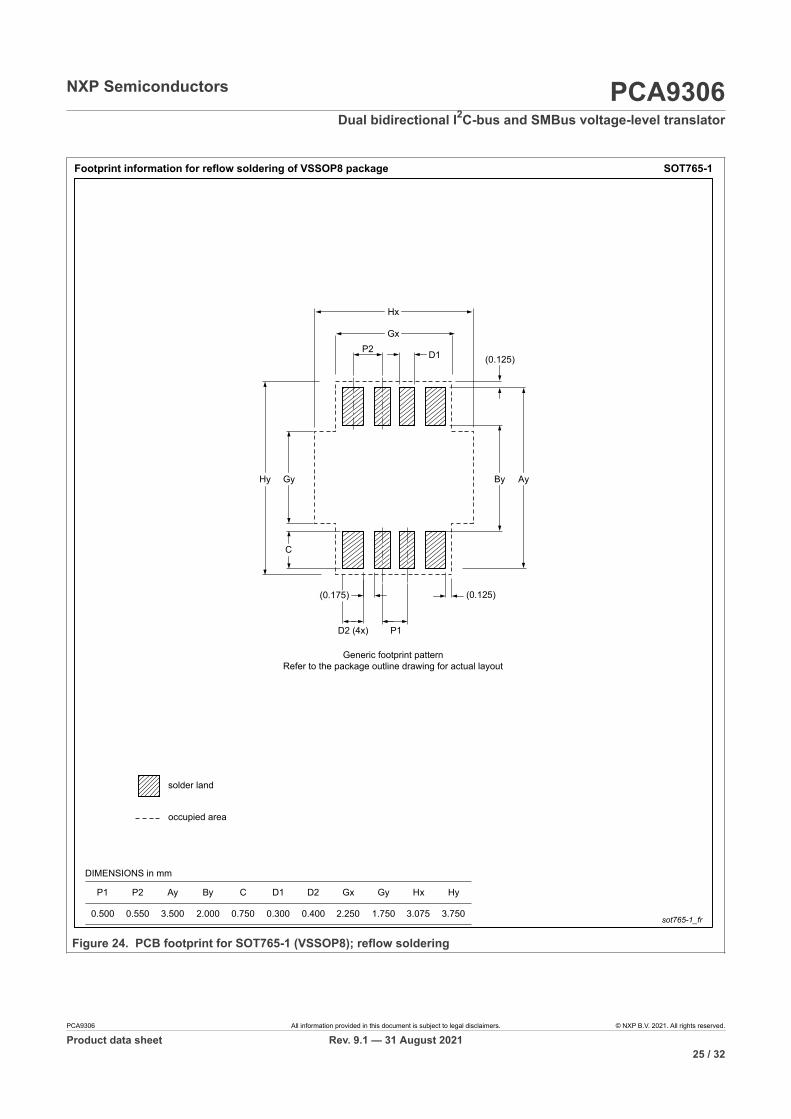
DIMENSIONS in mm
Ay By D1 D2 Gy HyP1
3.500 2.000 0.750 0.300
C
0.400 2.250 1.750
Gx
3.750sot765-1_fr
Hx
3.0750.500
SOT765-1Footprint information for reflow soldering of VSSOP8 package
AyByGy
C
Hy
Hx
Gx
P1
Generic footprint patternRefer to the package outline drawing for actual layout
P2
(0.125)
(0.125)D1
D2 (4x)
P2
0.550
solder land
occupied area
(0.175)
Figure 24. PCB footprint for SOT765-1 (VSSOP8); reflow soldering
PCA9306 All information provided in this document is subject to legal disclaimers. © NXP B.V. 2021. All rights reserved.
Product data sheet Rev. 9.1 — 31 August 202125 / 32
NXP Semiconductors PCA9306Dual bidirectional I2C-bus and SMBus voltage-level translator
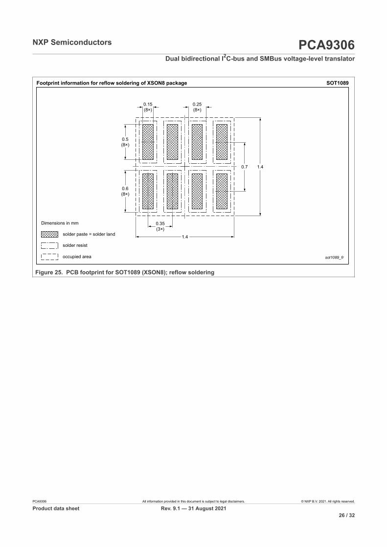
sot1089_fr
Footprint information for reflow soldering of XSON8 package SOT1089
solder resist
occupied area
solder paste = solder land
Dimensions in mm
0.15 (8×)
0.35 (3×)
0.25 (8×)
0.5 (8×)
0.6 (8×)
0.7 1.4
1.4
Figure 25. PCB footprint for SOT1089 (XSON8); reflow soldering
PCA9306 All information provided in this document is subject to legal disclaimers. © NXP B.V. 2021. All rights reserved.
Product data sheet Rev. 9.1 — 31 August 202126 / 32
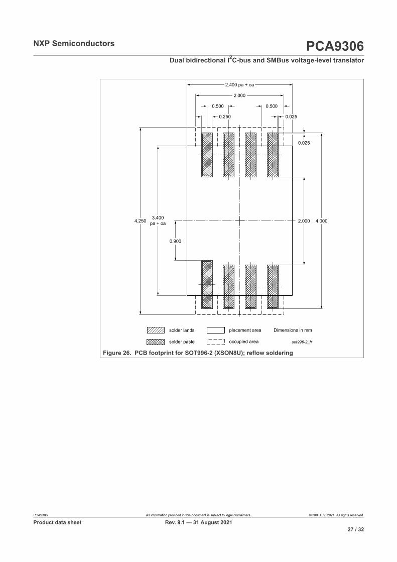
NXP Semiconductors PCA9306Dual bidirectional I2C-bus and SMBus voltage-level translator
placement area
occupied area
solder lands
solder paste
Dimensions in mm
sot996-2_fr
0.025
0.0250.250
2.000
2.000 4.0003.400
pa + oa4.250
0.900
2.400 pa + oa
0.5000.500
Figure 26. PCB footprint for SOT996-2 (XSON8U); reflow soldering
PCA9306 All information provided in this document is subject to legal disclaimers. © NXP B.V. 2021. All rights reserved.
Product data sheet Rev. 9.1 — 31 August 202127 / 32
NXP Semiconductors PCA9306Dual bidirectional I2C-bus and SMBus voltage-level translator
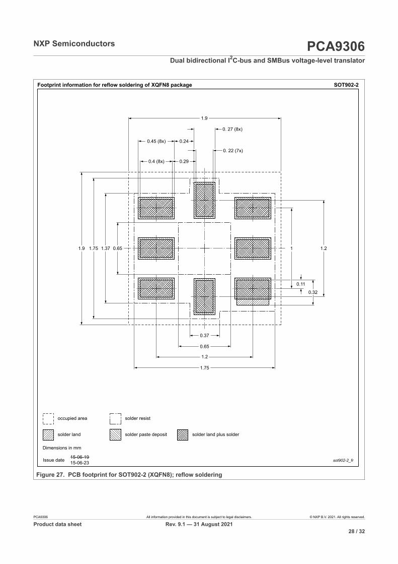
SOT902-2Footprint information for reflow soldering of XQFN8 package
sot902-2_frIssue date 15-06-1915-06-23
1.9
0.240.45 (8x)
0.4 (8x) 0.29
0.37
0.65
1.2
1.75
1 1.20.651.371.751.9
0.11
0.32
0. 22 (7x)
0. 27 (8x)
occupied area
solder paste deposit
solder resist
solder land solder land plus solder
Dimensions in mm
Figure 27. PCB footprint for SOT902-2 (XQFN8); reflow soldering
PCA9306 All information provided in this document is subject to legal disclaimers. © NXP B.V. 2021. All rights reserved.
Product data sheet Rev. 9.1 — 31 August 202128 / 32
NXP Semiconductors PCA9306Dual bidirectional I2C-bus and SMBus voltage-level translator
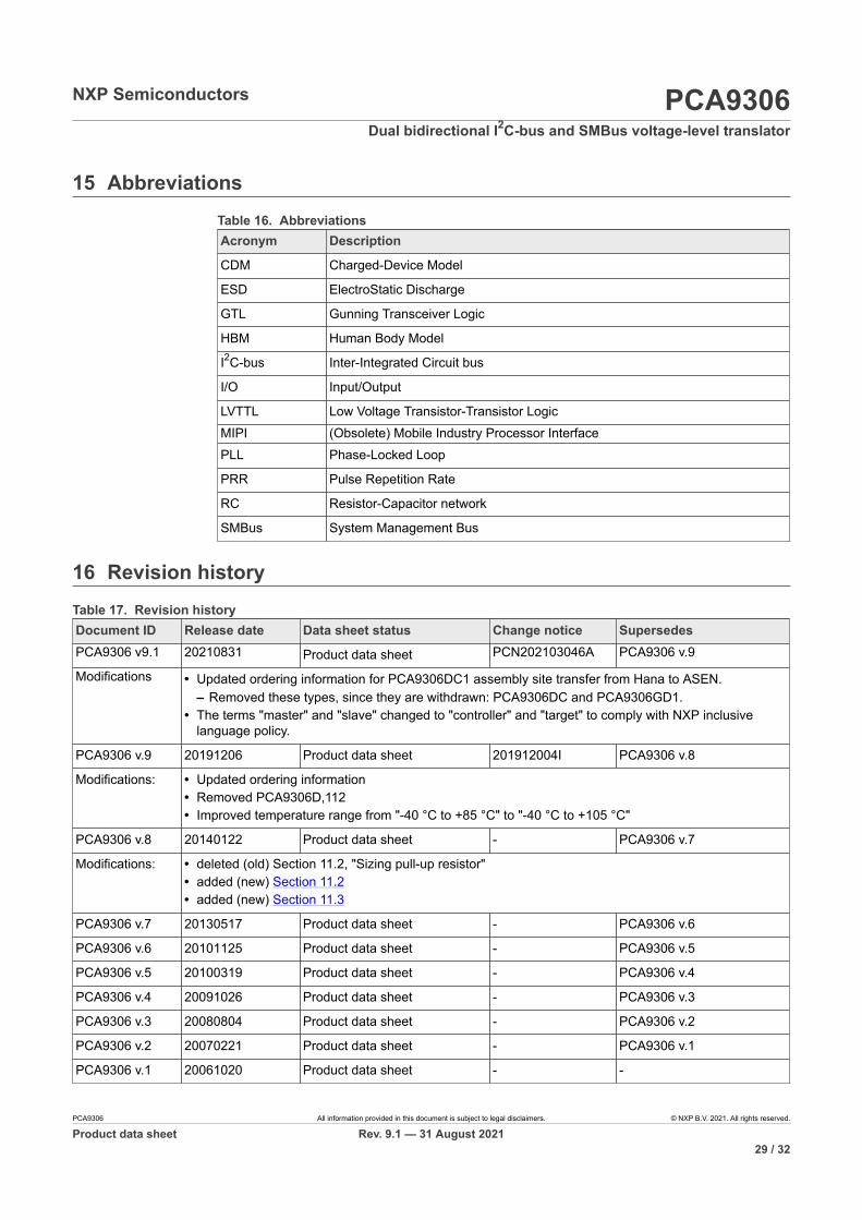
15 Abbreviations
Acronym Description
CDM Charged-Device Model
ESD ElectroStatic Discharge
GTL Gunning Transceiver Logic
HBM Human Body Model
I2C-bus Inter-Integrated Circuit bus
I/O Input/Output
LVTTL Low Voltage Transistor-Transistor LogicMIPI (Obsolete) Mobile Industry Processor InterfacePLL Phase-Locked Loop
PRR Pulse Repetition Rate
RC Resistor-Capacitor network
SMBus System Management Bus
Table 16. Abbreviations
16 Revision history
Document ID Release date Data sheet status Change notice SupersedesPCA9306 v9.1 20210831 Product data sheet PCN202103046A PCA9306 v.9
Modifications • Updated ordering information for PCA9306DC1 assembly site transfer from Hana to ASEN.– Removed these types, since they are withdrawn: PCA9306DC and PCA9306GD1.
• The terms "master" and "slave" changed to "controller" and "target" to comply with NXP inclusivelanguage policy.
PCA9306 v.9 20191206 Product data sheet 201912004I PCA9306 v.8
Modifications: • Updated ordering information• Removed PCA9306D,112• Improved temperature range from "-40 °C to +85 °C" to "-40 °C to +105 °C"
PCA9306 v.8 20140122 Product data sheet - PCA9306 v.7
Modifications: • deleted (old) Section 11.2, "Sizing pull-up resistor"• added (new) Section 11.2• added (new) Section 11.3
PCA9306 v.7 20130517 Product data sheet - PCA9306 v.6
PCA9306 v.6 20101125 Product data sheet - PCA9306 v.5
PCA9306 v.5 20100319 Product data sheet - PCA9306 v.4
PCA9306 v.4 20091026 Product data sheet - PCA9306 v.3
PCA9306 v.3 20080804 Product data sheet - PCA9306 v.2
PCA9306 v.2 20070221 Product data sheet - PCA9306 v.1
PCA9306 v.1 20061020 Product data sheet - -
Table 17. Revision history
PCA9306 All information provided in this document is subject to legal disclaimers. © NXP B.V. 2021. All rights reserved.
Product data sheet Rev. 9.1 — 31 August 202129 / 32
NXP Semiconductors PCA9306Dual bidirectional I2C-bus and SMBus voltage-level translator
17 Legal information
17.1 Data sheet status
Document status[1][2] Product status[3] Definition
Objective [short] data sheet Development This document contains data from the objective specification for productdevelopment.
Preliminary [short] data sheet Qualification This document contains data from the preliminary specification.
Product [short] data sheet Production This document contains the product specification.
[1] Please consult the most recently issued document before initiating or completing a design.[2] The term 'short data sheet' is explained in section "Definitions".[3] The product status of device(s) described in this document may have changed since this document was published and may differ in case of multiple
devices. The latest product status information is available on the Internet at URL http://www.nxp.com.
17.2 DefinitionsDraft — A draft status on a document indicates that the content is stillunder internal review and subject to formal approval, which may resultin modifications or additions. NXP Semiconductors does not give anyrepresentations or warranties as to the accuracy or completeness ofinformation included in a draft version of a document and shall have noliability for the consequences of use of such information.
Short data sheet — A short data sheet is an extract from a full data sheetwith the same product type number(s) and title. A short data sheet isintended for quick reference only and should not be relied upon to containdetailed and full information. For detailed and full information see therelevant full data sheet, which is available on request via the local NXPSemiconductors sales office. In case of any inconsistency or conflict with theshort data sheet, the full data sheet shall prevail.
Product specification — The information and data provided in a Productdata sheet shall define the specification of the product as agreed betweenNXP Semiconductors and its customer, unless NXP Semiconductors andcustomer have explicitly agreed otherwise in writing. In no event however,shall an agreement be valid in which the NXP Semiconductors productis deemed to offer functions and qualities beyond those described in theProduct data sheet.
17.3 Disclaimers
17.4 TrademarksNotice: All referenced brands, product names, service names andtrademarks are the property of their respective owners.
PCA9306 All information provided in this document is subject to legal disclaimers. © NXP B.V. 2021. All rights reserved.
Product data sheet Rev. 9.1 — 31 August 202130 / 32
NXP Semiconductors PCA9306Dual bidirectional I2C-bus and SMBus voltage-level translator
TablesTab. 1. Ordering information ..........................................2Tab. 2. Ordering options ................................................3Tab. 3. Pin description ...................................................4Tab. 4. Function selection (example) ............................ 5Tab. 5. Limiting values .................................................. 5Tab. 6. Operating conditions ......................................... 6Tab. 7. Static characteristics ......................................... 6Tab. 8. Dynamic characteristics (translating down) ....... 7Tab. 9. Dynamic characteristics (translating up) ............7Tab. 10. Application operating conditions ........................9Tab. 11. Pull-up resistor minimum values, 3 mA
driver sink current for PCA9306 andNVT20xx ..........................................................10
Tab. 12. Pull-up resistor minimum values, 10 mAdriver sink current for PCA9306 andNVT20xx ..........................................................11
Tab. 13. Pull-up resistor minimum values, 15 mAdriver sink current for PCA9306 andNVT20xx ..........................................................11
Tab. 14. SnPb eutectic process (from J-STD-020D) ..... 21Tab. 15. Lead-free process (from J-STD-020D) ............ 21Tab. 16. Abbreviations ...................................................29Tab. 17. Revision history ...............................................29
FiguresFig. 1. Logic diagram of PCA9306 (positive logic) ........3Fig. 2. Pin configuration for TSSOP8 (DP1) .................4Fig. 3. Pin configuration for TSSOP8 (DP)
(MSOP8) ............................................................4Fig. 4. Pin configuration for VSSOP8 (DC1; DC1/
DG) ....................................................................4Fig. 5. Pin configuration for SO8 ..................................4Fig. 6. Pin configuration for XQFN8 ............................. 4Fig. 7. Pin configuration for XSON8 .............................4Fig. 8. Load circuit for outputs ..................................... 8Fig. 9. Typical application circuit (switch always
enabled) .............................................................8Fig. 10. Typical application circuit (switch enable
control) ...............................................................9Fig. 11. An example waveform for maximum
frequency .........................................................12Fig. 12. Package outline SOT96-1 (SO8) .....................13Fig. 13. Package outline SOT505-1 (TSSOP8) ............14Fig. 14. Package outline SOT505-2 (TSSOP8) ............15Fig. 15. Package outline SOT765-1 (VSSOP8) ............16Fig. 16. Package outline SOT902-2 (XQFN8) ..............17
Fig. 17. Package outline SOT1089 (XSON8) ...............18Fig. 18. Package outline SOT996-2 (XSON8U) ........... 19Fig. 19. Temperature profiles for large and small
components .....................................................22Fig. 20. PCB footprint for SOT96-1 (SO8); reflow
soldering ..........................................................22Fig. 21. PCB footprint for SOT96-1 (SO8); wave
soldering ..........................................................23Fig. 22. PCB footprint for SOT505-1 (TSSOP8);
reflow soldering ............................................... 23Fig. 23. PCB footprint for SOT505-2 (TSSOP8);
reflow soldering ............................................... 24Fig. 24. PCB footprint for SOT765-1 (VSSOP8);
reflow soldering ............................................... 25Fig. 25. PCB footprint for SOT1089 (XSON8);
reflow soldering ............................................... 26Fig. 26. PCB footprint for SOT996-2 (XSON8U);
reflow soldering ............................................... 27Fig. 27. PCB footprint for SOT902-2 (XQFN8);
reflow soldering ............................................... 28
PCA9306 All information provided in this document is subject to legal disclaimers. © NXP B.V. 2021. All rights reserved.
Product data sheet Rev. 9.1 — 31 August 202131 / 32
NXP Semiconductors PCA9306Dual bidirectional I2C-bus and SMBus voltage-level translator
Contents1 General description ............................................ 12 Features and benefits .........................................23 Ordering information .......................................... 23.1 Ordering options ................................................ 34 Functional diagram ............................................. 35 Pinning information ............................................ 45.1 Pinning ...............................................................45.2 Pin description ................................................... 46 Functional description ........................................56.1 Function table .................................................... 57 Limiting values ....................................................58 Recommended operating conditions ................ 69 Static characteristics .......................................... 610 Dynamic characteristics .....................................711 Application information ......................................811.1 Bidirectional translation ......................................911.2 How to size pull-up resistor value ....................1011.3 How to design for maximum frequency
operation ..........................................................1112 Package outline .................................................1313 Soldering of SMD packages .............................2013.1 Introduction to soldering .................................. 2013.2 Wave and reflow soldering .............................. 2013.3 Wave soldering ................................................ 2013.4 Reflow soldering .............................................. 2014 Soldering: PCB footprints ................................2215 Abbreviations .................................................... 2916 Revision history ................................................ 2917 Legal information ..............................................30
Please be aware that important notices concerning this document and the product(s)described herein, have been included in section 'Legal information'.
© NXP B.V. 2021. All rights reserved.For more information, please visit: http://www.nxp.comFor sales office addresses, please send an email to: [email protected]
Date of release: 31 August 2021Document identifier: PCA9306
Mouser Electronics
Authorized Distributor
Click to View Pricing, Inventory, Delivery & Lifecycle Information: NXP:
PCA9306DC1,125 PCA9306DC,125 PCA9306DP1,125 PCA9306DP,118 PCA9306D,118 PCA9306GM,125
PCA9306D,112 PCA9306GF,115 PCA9306GD1,125 PCA9306DC1/DG,125 PCA9306DC1-G PCA9306GM-G
PCA9306DP1