lowlow--power power designdesign (()lpd) - eurasip · lowlow--power power designdesign (()lpd)...
TRANSCRIPT

LowLow--Power Power DesignDesign(LPD)(LPD)( )( )
Eduardo BoemoEduardo BoemoEduardo BoemoEduardo Boemo
EUROFORM TECHNICAL EUROFORM TECHNICAL TRAININGTRAINING
Escuela Politécnica Superior Escuela Politécnica Superior scue a o éc ca Supe oscue a o éc ca Supe oUniversidad Autónoma de MadridUniversidad Autónoma de Madrid
ee--mail:[email protected]:[email protected]/~ivanwww.ii.uam.es/~ivan
h // ii / f /h // ii / f /http://arantxa.ii.uam.es/~euroform/http://arantxa.ii.uam.es/~euroform/
© 2012, [email protected]
11
DynamicDynamic Power = c f VPower = c f V22
ΣΣ NodeNode capacitancecapacitance xx NodeNode frequencyfrequency xx NodeNode VoltageVoltage22
00 11:: EnergyEnergy = 1/2 C V= 1/2 C V2 2 00 11:: EnergyEnergycapcap = 1/2 C V= 1/2 C V
EnergyEnergytotatota ll= C V= C V22
EnergyEnergyPP--trantran= 1/2 C V= 1/2 C V22P
11 00:: EnergyEnergyNN--trantran= 1/2 C V= 1/2 C V22
Dynamic Power:Dynamic Power:N
P = Energy / Time = E . f = C.f.V2
(if the node reach V and GND completely)(if the node reach V and GND completely)
© 2012, [email protected]
22
(if the node reach V and GND completely)(if the node reach V and GND completely)

Other power components:Other power components:Other power components: Other power components: Dynamic … + Short Circuit + LeakageDynamic … + Short Circuit + Leakage
PPtotaltotal = = CCLL f Vf VDDDD22 + + VVDDDD IIscsc ++ VVDD DD IIleakageleakage
VDD VDD
CCL
Source: http://www.eng.auburn.edu/~vagrawal
© 2012, [email protected]
33
Power components: Structural classificationPower components: Structural classificationPower components: Structural classificationPower components: Structural classification
Dynamic Power:
• Clock power: Power in the clock tree and FFs.
• Off-chip power: Power in the output pads. Off-chip capacitances are 1000 times bigger. Is not a function of the FPGA model.are 1000 times bigger. Is not a function of the FPGA model.
• Datapath power: Power of the logic that process the data.
Static Power: DC Power (fclk=0)
• Raw FPGA.C fi d FPGA• Configured FPGA.
Configuration power
© 2012, [email protected]
44
Configuration power.

Power Figure in 2012 FPGAsPower Figure in 2012 FPGAsPower Figure in 2012 FPGAsPower Figure in 2012 FPGAs
Example:
• Traffic Manager in 100G Line • Traffic Manager in 100G Line Card Virtex-7 VX550T .
• Source: 7-series-power-benchmark-summary.pdf Xilinx Inc, Dec 2012
© 2012, [email protected]
55
Dynamic Power: Effective frequencyDynamic Power: Effective frequencyDynamic Power: Effective frequencyDynamic Power: Effective frequency
TheThe f f isis thethe frequencyfrequency of of eacheach nodenode ((notnot systemsystem A B A.B A+B AB
ffCLKCLK).).
ff
0 0 0 0 0
ThereThere isis anan activityactivity factorfactorf = f = ffCLKCLK
0 1 0 1 1
1 0 0 1 1 TheThe activityactivity factor factor
dependdepend onon thethe logiclogic
1 0 0 1 1
1 1 1 1 0dependdepend onon thethe logiclogicfunctionsfunctions and and thethe input input datadata
1 1 1 1 0
ExampleExample
Prob 0-1 = P0.P1 is different in each case
© 2012, [email protected]
66

DynamicDynamic Power: Power: EffectiveEffective frequencyfrequency andand glitchesglitchesEffectiveEffective frequencyfrequency and and glitchesglitches
GlitchesGlitches are spurious are spurious transitions due to transitions due to different delaysdifferent delaysdifferent delays.different delays.
GlitchesGlitches generate generate ggactivity producing a activity producing a snowsnow--ball effectball effect
In FPGA technology In FPGA technology glitch power depend glitch power depend on the PPR.on the PPR.
The contribution of The contribution of The contribution of The contribution of glitches to the total glitches to the total power is huge.power is huge.
© 2012, [email protected]
77
Xilinx strategies to minimize dynamic powerXilinx strategies to minimize dynamic powerXilinx strategies to minimize dynamic powerXilinx strategies to minimize dynamic power
© 2012, [email protected]
88

Xilinx strategies to minimize static powerXilinx strategies to minimize static powerg pg p
© 2012, [email protected]
99
OffOff--chip Powerchip Powerpp
1985 databook
C x f x V2 50 pF x f x 25 v2 1250 10 12 106 x f [MH] C x f x V2 = 50 pF x f x 25 v2 = 1250 10-12 106 x f [MH]
watts/MHz = 1,25 mW/MHz
The off-chip power (pins) does not depend on –excepting V - the
scale integration. It is simply caused by 2 transistors (inside the
© 2012, [email protected]
1010chip) that charge/descharge a capacitance (outside the chip).

OffOff--chip power: Xilinx LPD strategieschip power: Xilinx LPD strategiesOffOff chip power: Xilinx LPD strategieschip power: Xilinx LPD strategies
© 2012, [email protected]
1111Discussion: slew-rate, driving capability, power, and energy.
Synchronization power : Current FPGAsSynchronization power : Current FPGAsSynchronization power : Current FPGAsSynchronization power : Current FPGAs
•• HighHigh--speed speed Pipelining Pipelining great number of registersgreat number of registers
•• Registers Registers conmuteconmute at at ffClockClock (if clock gating is not applied)(if clock gating is not applied)gg ClockClock ( g g pp )( g g pp )
•• TheThe sinchronizationsinchronization powerpower isis a linear a linear functionfunction of of thetheproductproduct #FF x #FF x ffCLKCLK..
© 2012, [email protected]
1212

Power analysis and measurement at system levelPower analysis and measurement at system levely yy y
PCB must be designed with some of the following PCB must be designed with some of the following characteristics:characteristics:
P l t i l t b ibl d t dP l t i l t b ibl d t d•• Power supply terminals must be accessible and separated.Power supply terminals must be accessible and separated.
I i l b d i ibl t thi I i l b d i ibl t thi In commercial board is possible to overcome this In commercial board is possible to overcome this problem removing the voltage regulators.problem removing the voltage regulators.
•• Possibility of stop/replace clock signal.Possibility of stop/replace clock signal.•• ““SeparativitySeparativity” of power supply by functional blocks.” of power supply by functional blocks.SeparativitySeparativity of power supply by functional blocks. of power supply by functional blocks.•• External control of different chip outputExternal control of different chip output--enable signals.enable signals.
Scaling in frequency is possible.Scaling in frequency is possible.
© 2012, [email protected]
1313
Power analysis and measurement at system Power analysis and measurement at system levellevel
Source: G. Gonzalez de Rivera, J. Garrido, and E. Boemo, "Power Audit of an Space-Certified Microprocessor", Proc PATMOS'99 (International Workshop Power and Timing Modeling, Optimization and Simulation), pp.551-556, October 6-8, Kos Island, Greece
ROMVCC
Five independent power supply lines:
a) the microprocessor
ADDRESSCONVERTER
RESET
µPADDRESS BUS
CONTROL BUS
GLUELOGIC
a) t e c op ocesso
b) the 8KB ROM
c) the 8KB RAM
RAM
CLOCK
DATA BUS
d) address converters
e) the miscellaneous . logic.CLOCK ADDRESS
DECODER
. logic.
Different voltages can be
CONFIGURATIONREGISTER
LED ARRAY
applied to each block.
© 2012, [email protected]
1414

Power analysis and measurement at system levelPower analysis and measurement at system levelExampleExampleExampleExample
OSCILLATORS LEDs
CONFIGURATIONSWITCHES
INDICATORS
EXTRASOCKETS
TESTPOINTS
MICROPROCESSOR
SOCKETS
ADDRESSCONVERTER
ADDRESSDECODER
MEASURE
EXPANSIONBUS
ADDRESS BUSCONNECTORS
ROM
RAM
MEASUREBRIDGES
Source: G. Gonzalez de Rivera, J. Garrido, and E. Boemo, "Power Audit of an Space-Certified Mi " P PATMOS'99 (I t ti l W k h P d Ti i M d li
© 2012, [email protected]
1515
Microprocessor", Proc PATMOS'99 (International Workshop Power and Timing Modeling, Optimization and Simulation), pp.551-556, October 6-8, Kos Island, Greece
Power analysis at chip levelPower analysis at chip levelPower analysis at chip levelPower analysis at chip level
M j d
FPU10%
Manejo de Memoria
8%I/O5%
Misc.2%
IEU10%
• ← Alpha 21264. Source: [Gow98]10% ← Alpha 21264. Source: [Gow98]
Instruc.18%
caches15% Clock18%15%
32%
← Intel: Source: [Tiw98]
© 2012, [email protected]
1616

P l i t hi l lP l i t hi l lPower analysis at chip levelPower analysis at chip level
Source: E. Todorovich, G. Sutter, N. Acosta, E. Boemo and S. Lopez-Buedo, "End-user low-power alternatives at topological and physical levels. Some examples on FPGAs", Proc. p p g p y p ,DCIS'2000 (XV Conference on Design of Circuits and Integrated Systems), pp.640-644, Montpellier, November 21-24, 2000
© 2012, [email protected]
1717
Measuring powerMeasuring powerMeasuring powerMeasuring power
Average power: Average power: AmperimeterAmperimeter Average power: Average power: AmperimeterAmperimeter
•• The simple approach to measure The simple approach to measure IccIcc is to connect is to connect an ammeter an ammeter in series with the supplying pins. in series with the supplying pins.
•• Periodic input pattern must be to the DUT. Thus, the resulting Periodic input pattern must be to the DUT. Thus, the resulting current waveform is periodic. current waveform is periodic. current waveform is periodic. current waveform is periodic.
•• The ammeter averages the power supply current over a The ammeter averages the power supply current over a window of time and, if the period of the current waveform is window of time and, if the period of the current waveform is
h ll th thi i dh ll th thi i dmuch smaller than this window.much smaller than this window.
Dynamic Power (Method 1): Dynamic Power (Method 1):
•• Shunt Resistor + scope with differential probeShunt Resistor + scope with differential probe•• R between 2 and 100 R between 2 and 100 ΩΩ
© 2012, [email protected]
1818

Measuring clockMeasuring clock--byby--clock dynamic powerclock dynamic powerMeasuring clockMeasuring clock byby clock dynamic powerclock dynamic power
CDD= 10 nF
Source:
J. Rius-Vazquez, E. Boemo, A. PeidroPalanca, S. Manich-Bou and R. Rodriguez-Montañes, "Measuring Power and Energy of CMOS CIrcuits: A Comparative Analysis", Proceedings DCIS 2003 (XVIII Conference on Design of Circuits and Integrated Systems), pp. 89-94, Ciudad Real, November 2003.
© 2012, [email protected]
1919
Measuring power: Measuring power: A il tA il t N6705B DC PN6705B DC P A lA lAgilent Agilent N6705B DC Power N6705B DC Power AnalyzerAnalyzer
4 power supply4 power supply Voltmeter accuracy:Voltmeter accuracy: Up to 0.025% + 50 µV, up to 18 bitsUp to 0.025% + 50 µV, up to 18 bits Ammeter accuracy:Ammeter accuracy: Up to 0.025% + 8 Up to 0.025% + 8 nAnA, up to 18 bits, up to 18 bits Arbitrary waveform generator function:Arbitrary waveform generator function: Bandwidth up to 100 kHz, output Bandwidth up to 100 kHz, output
power up to 300 Wpower up to 300 Wp pp p Scope function:Scope function: Digitizes voltage and current at up to 200 kHz, up to 18 bitsDigitizes voltage and current at up to 200 kHz, up to 18 bits Data logger function:Data logger function: Measurement interval from 20 µs to 60 s.Measurement interval from 20 µs to 60 s.
© 2012, [email protected]
2020
AA reviewreview ofof somesome LPD ideasLPD ideas toto reducereduceA A reviewreview of of somesome LPD ideas LPD ideas toto reduce reduce DynamicDynamic PowerPower
P = P = ΣΣ c f vc f v2
Dense LUT utilization: ΣΣ ((lessless nodesnodes)) c (c (lessless wireswires))
ParallelismParallelism-- PipeliningPipelining ΣΣ ((biggerbigger nodenode countcount)) c (c (differentdifferent wirewire countcount) ) c (c (lessless wireswires))
f (f (lessless glitchesglitches))
DifferentDifferent topologiestopologies::
c (c (d e ed e e ee coucou )) c (c (differentdifferent fanoutfanout)) f (f (lessless glitchesglitches in in pipeliningpipelining)) V (V (thethe lowerlower can can bebe selectedselected))DifferentDifferent topologiestopologies::
ΣΣ ((differentdifferent nodenode countcount)) c (c (differentdifferent wirewire countcount
c (c (differentdifferent fanoutfanout))
V (V (thethe lowerlower can can bebe selectedselected))
PhysicalPhysical DesignDesign forfor highhigh--speedspeed c (c (differentdifferent fanoutfanout))
Manual Placement
speedspeed c (c (differentdifferent wirewire lengthlength) ) c (c (differentdifferent fanoutfanout))
V (V (thethe lo elo e can can bebe selectedselected)) c (c (lessless wirewire lengthlength oror
capacitancecapacitance)) V (V (thethe lowerlower can can bebe selectedselected))
ClockClock gatinggating //loweringlowering clockclock
© 2012, [email protected]
2121
f (f (lessless activityactivity))
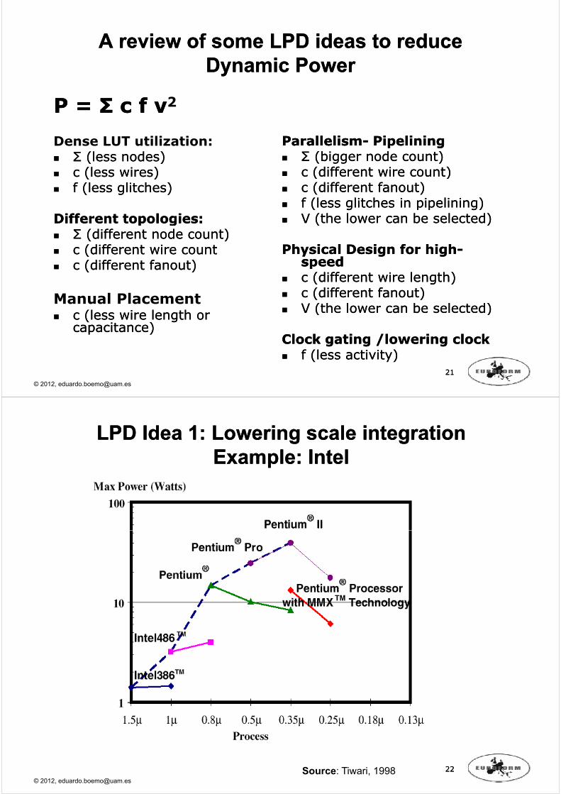
LPD Idea 1: LPD Idea 1: LoweringLowering scalescale integrationintegrationExampleExample: : IntelIntel
© 2012, [email protected]
2222Source: Tiwari, 1998

LPD Idea 1: LPD Idea 1: LoweringLowering scalescale integrationintegrationExampleExample:: Xilinx SpartanXilinx SpartanExampleExample: : Xilinx SpartanXilinx Spartan
DiscussionDiscussion: Scaling change the components of the power. : Scaling change the components of the power. Example: shortExample: short circuit is circuit is 11 16% power at 0 7 micron 416% power at 0 7 micron 4 37% at 0 35 37% at 0 35 Example: shortExample: short--circuit is circuit is 11--16% power at 0.7 micron, 416% power at 0.7 micron, 4--37% at 0.35 37% at 0.35 micron, 12micron, 12--60% at 0.17 micron60% at 0.17 micron
SourceSource: S R : S R VemuruVemuru and N Steinberg “Short Circuit Power Dissipation Estimation for CMOS Logic and N Steinberg “Short Circuit Power Dissipation Estimation for CMOS Logic
© 2012, [email protected]
2323
SourceSource: S. R. : S. R. VemuruVemuru and N. Steinberg, Short Circuit Power Dissipation Estimation for CMOS Logic and N. Steinberg, Short Circuit Power Dissipation Estimation for CMOS Logic Gates,” Gates,” IEEE Trans. on Circuits and Systems IIEEE Trans. on Circuits and Systems I, vol. 41, Nov. 1994, pp. 762, vol. 41, Nov. 1994, pp. 762--765.765.
LPD Idea 2: Lowering Power Supply LPD Idea 2: Lowering Power Supply (Xili )(Xili )(Xilinx)(Xilinx)
“… Since the “… Since the VirtexVirtex--5 FPGA can 5 FPGA can operate within its operate within its specifications even specifications even specifications even specifications even with a voltage of with a voltage of 0.95V, some 0.95V, some power benefit can power benefit can power benefit can power benefit can be achieved by be achieved by adjusting VCCINT adjusting VCCINT t li htl b l t li htl b l to slightly below to slightly below the nominal the nominal voltage, such as voltage, such as 0.98V”.0.98V”.
P static ~ kVP static ~ kV33 P static ~ kVP static ~ kV33
∆∆V acceptable = V acceptable = ±±5%5%
Source: P. Abusaidi, M. Klein, and B. Philofsky, Virtex-5 FPGA S t P D i C id ti Xili I 2008
© 2012, [email protected]
5%5%2424
System Power Design Considerations, Xilinx Inc. 2008
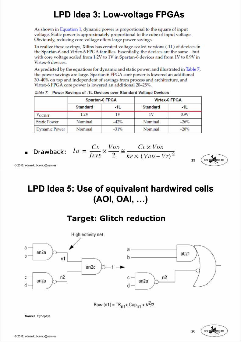
LPD Idea 3: LowLPD Idea 3: Low--voltage FPGAsvoltage FPGAs
D b kD b k
© 2012, [email protected]
2525
Drawback:Drawback:
LPD Idea 5: Use of equivalent hardwired cellsLPD Idea 5: Use of equivalent hardwired cellsLPD Idea 5: Use of equivalent hardwired cells LPD Idea 5: Use of equivalent hardwired cells (AOI, OAI, …)(AOI, OAI, …)
Target: Glitch reduction
Source: Synopsys
© 2012, [email protected]
2626

LPD Idea 5 (in FPGA): Use of equivalent hardLPD Idea 5 (in FPGA): Use of equivalent hard--LPD Idea 5 (in FPGA): Use of equivalent hardLPD Idea 5 (in FPGA): Use of equivalent hardmacrosmacros
DiscussionDiscussion: What can be deduced from this Xilinx text?: What can be deduced from this Xilinx text?
Answer: The extra power of FPGA respect to CBIC canbe nearly a 10x factor.
© 2012, [email protected]
2727
LPD Idea 6: LPD Idea 6: Dense utilization of LUTsDense utilization of LUTs
•• Manual Manual partitioningpartitioning or dense occupationor dense occupation(CLBMAP FMAP (CLBMAP FMAP •• Manual Manual partitioningpartitioning or dense occupationor dense occupation(CLBMAP, FMAP, (CLBMAP, FMAP, HMAP, LOC, etc.) HMAP, LOC, etc.) isis alsoalso effectiveeffective..–– # # LUTsLUTs –– LogicLogic depthdepth –– # # NodesNodes –– WiringWiring delaydelay –– ButBut … P … P
© 2012, [email protected]
2828

LPD Idea 7:LPD Idea 7:Reordering of high activity signalsReordering of high activity signals
ram
(U
SC
)o
urc
e: P
edr
So
Idea: The faster signal as near the output as possible
© 2012, [email protected]
2929
LPD Idea 8:LPD Idea 8: Special Place&Route of Special Place&Route of hi h ti it dhi h ti it dhigh activity nodeshigh activity nodes
Source:Source:
E E TodorovichTodorovich E E BoemoBoemo F F E. E. TodorovichTodorovich, E. , E. BoemoBoemo, F. , F. AngaritaAngarita, and J. , and J. VallsValls, , "Statistical power estimation for "Statistical power estimation for FPGAs", FPGAs", FPL 2005 (XV FPL 2005 (XV International Conference on International Conference on International Conference on International Conference on Field Programmable Logic and Field Programmable Logic and Applications)Applications), pp.515 , pp.515 -- 518, 518, Tampere, Finland, August 2005. Tampere, Finland, August 2005. IEEE P e ISBN 0IEEE P e ISBN 0 78037803 93629362IEEE Press. ISBN: 0IEEE Press. ISBN: 0--78037803--93629362--7 7
IdeaIdea: To minimize wire capacitance of high: To minimize wire capacitance of high--activity nodesactivity nodes
ActionsActions:: ActionsActions:: Simulation to detect the candidate nodes.Simulation to detect the candidate nodes. FloorplanningFloorplanning.. PPR manual (Xilinx)PPR manual (Xilinx)
© 2012, [email protected]
3030
PPR manual (Xilinx)PPR manual (Xilinx) Time specification to the automatic PPRTime specification to the automatic PPR

LPD Idea 8:LPD Idea 8: Special Place&Route Special Place&Route of high activity nodesof high activity nodes
SourceSource: Elias : Elias TodorovichTodorovich PhD Thesis UAM 2006PhD Thesis UAM 2006
© 2012, [email protected]
3131
SourceSource: Elias : Elias TodorovichTodorovich PhD Thesis , UAM 2006PhD Thesis , UAM 2006
LPD Id 9LPD Id 9 B /St t C diB /St t C diLPD Idea 9: LPD Idea 9: Bus/State CodingBus/State Coding
Source: Jonathan Alexande, Actel Corporation
© 2012, [email protected]
3232
LPD Id 9LPD Id 9 B /St t C diB /St t C diLPD Idea 9: LPD Idea 9: Bus/State CodingBus/State Coding
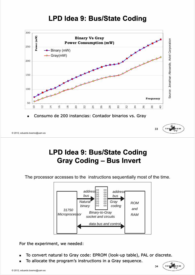
Binary Vs GrayPower Consumption (mW)
250
300w
er
(mW
)
orat
ion
200
250
Pow
Binary (mW)
Gray(mW)
Acte
l Cor
po
150
200
n Al
exan
de,
100 e: J
onat
han
50
0 2 4 6 8 0 2 4 6 8 0 2 4 6 8 0
Frequency Sour
ce
ConsumoConsumo de 200 de 200 instanciasinstancias: : ContadorContador binariosbinarios vs. Grayvs. Gray
10
12
14
16
18
20
22
24
26
28
30
32
34
36
38
40
© 2012, [email protected]
3333
LPD Idea 9:LPD Idea 9: Bus/State CodingBus/State CodingLPD Idea 9: LPD Idea 9: Bus/State CodingBus/State CodingGray Coding Gray Coding –– Bus InvertBus Invert
The processor accesses to the instructions sequentially most of the time.
addressbus
addressbus
Graycoding
Naturalbinary
Binary-to-Gray
ROM
and
RAM31750
Mi
data bus and control
Binary to Graysocket and circuits RAMMicroprocessor
For the experiment we needed:For the experiment we needed:For the experiment, we needed:For the experiment, we needed:
To convert natural to Gray code: EPROM (lookTo convert natural to Gray code: EPROM (look--up table), PAL or discrete.up table), PAL or discrete.
© 2012, [email protected]
3434
To allocate the program’s instructions in a Gray sequence.To allocate the program’s instructions in a Gray sequence.

LPD Idea 10:LPD Idea 10: GlitchGlitch reductionreduction byby pipeliningpipeliningLPD Idea 10:LPD Idea 10: GlitchGlitch reductionreduction byby pipeliningpipeliningExampleExample XilinxXilinx
© 2012, [email protected]
3535
LPD Idea 10:LPD Idea 10: GlitchGlitch reductionreduction byby pipeliningpipeliningLPD Idea 10:LPD Idea 10: GlitchGlitch reductionreduction byby pipeliningpipeliningExampleExample Actel and AlteraActel and Altera
© 2012, [email protected]
3636

LPD Idea 10:LPD Idea 10: GlitchGlitch reductionreduction byby pipeliningpipeliningLPD Idea 10:LPD Idea 10: GlitchGlitch reductionreduction byby pipeliningpipelining
Source. E. Boemo, PhD Thesis, 1996
360
380
400
A
@ 5 MHzC
out < 10 pF per pad
tiedrandom vectors)
Xilinx 3K y 4K
280
300
320
340
C
e po
wer
pt
ion
(mW
)
220
240
260
280
B
aver
agco
nsum
p
1 2 4 8 15
180
200
220 B
1 2 4 8 15
pipeline granularity 32 FF146 CLB
200 FF205 CLB
• A: XC3090, default PPR.
• B: XC3090, manual partitioning en LUTs.
• C: XC4005 default PPR
© 2012, [email protected]
3737
• C: XC4005, default PPR
LPD Idea 10:LPD Idea 10: GlitchGlitch reductionreduction byby pipeliningpipeliningLPD Idea 10: LPD Idea 10: GlitchGlitch reductionreduction byby pipeliningpipeliningSource. E. Boemo, PhD Thesis, 1996
240
Altera FLEX81188CG232-3Moderate
220
240
@ 5 MHzC
out < 10 pF
random vectors
W)
Moderate pipelining reduce significantly the
200
ge p
ower
mpt
ion
(mW power in all
FPGAs
160
180
aver
agco
nspu
m
10 years
3 series
140
160 3 series
3 manufacturers.
1 2 4 8 15
pipeline granularity
© 2012, [email protected]
3838

LPD Idea 10: LPD Idea 10: GlitchGlitch reductionreduction byby pipeliningpipeliningAA P ltP ltAreaArea PenaltyPenalty
Alex Caraba “Analysis of FPGA programmable devices in Alex Caraba, Analysis of FPGA – programmable devices in 0.45 nm technology” Master Thesis – UAM, 2011
© 2012, [email protected]
3939
LPD Idea 10:LPD Idea 10: GlitchGlitch reductionreduction byby pipeliningpipeliningLPD Idea 10: LPD Idea 10: GlitchGlitch reductionreduction byby pipeliningpipeliningAreaArea PenaltyPenalty
© 2012, [email protected]
4040

LPD Idea 10:LPD Idea 10: GlitchGlitch reductionreduction byby pipeliningpipeliningConclusionsConclusions
• Power reduction up to:
• - 33 % (XC3090) ( )
• - 58 % (XC4005)
• - 85 % (Virtex)
• - 30 % (Altera Flex)- 30 % (Altera Flex)
• Cost:
N b f i t• Number of registers
• Latency
• Manual partitioning (CLBMAP, FMAP, HMAP, LOC, etc.) is also effective.
– LUTs – Logic depth – Nodes – Wiring delay – But … P
© 2012, [email protected]
4141
But … P
LPD Idea 10:LPD Idea 10: Pipelining as LPD TechniquePipelining as LPD TechniqueLPD Idea 10:LPD Idea 10: Pipelining as LPD Technique Pipelining as LPD Technique (Actel)(Actel)
© 2012, [email protected]
4242

LPD Idea 11:LPD Idea 11: Path equalization to reducePath equalization to reduceLPD Idea 11:LPD Idea 11: Path equalization to reduce Path equalization to reduce glitches glitches WP (Wave Pipeline)WP (Wave Pipeline)
© 2012, [email protected]
4343
LPD Idea 11:LPD Idea 11: Path equalization to reduce Path equalization to reduce lit hlit h WP (W Pi li )WP (W Pi li )glitches glitches WP (Wave Pipeline)WP (Wave Pipeline)
2500
3000
combinacional(no balanceado)W
)
1500
2000
wave pipeline
(no balanceado)
pote
ncia
(m
W
500
1000
XC4005PC84-100
= 1 convencional
cons
umo
de
0 20 40 60 800
XC4005PC84 100Guild, n=7
MOPS
E. Boemo, S. Lopez-Buedo, and J. Meneses, "Some Experiments about Wave Pipelining on FPGAs",Experiments about Wave Pipelining on FPGAs , IEEE Transactions on Very Large Scale Integration (VLSI) Systems, Vol.6, No.2, June 1998.
© 2012, [email protected]
4444
WP doesn't work as LPD strategy.

LPD Idea 12:LPD Idea 12: More BWMore BW Less PowerLess PowerLPD Idea 12:LPD Idea 12: More BW More BW -- Less PowerLess Power
Peter Peter AlfkeAlfke idea: more idea: more
1 6
1.8 Note: Power @ 5 MHz
mpt
ion
speed need lower wire speed need lower wire capacitances, and lower capacitances, and lower wire capacitances lead to wire capacitances lead to
1.4
1.6
wer
con
sum
less powerless power
←← Power versus Power versus minimunminimun
1 0
1.2
mal
ized
pow ← ← Power versus Power versus minimunminimun
clock period reachable clock period reachable of identical multipliers of identical multipliers with different PPRs with different PPRs
0 1 2 3 4 5 6 7 8 9 100.8
1.0
Nor
m with different PPRs with different PPRs
SourceSource:: ““ContribuciónContribución al al DiseñoDiseño de de Arrays VLSI”Arrays VLSI” E Boemo UPM: 1995E Boemo UPM: 1995
Normalized bandwidth-1
Arrays VLSI ,Arrays VLSI , E. Boemo, UPM: 1995.E. Boemo, UPM: 1995.
Minimum clock period achieved
© 2012, [email protected]
4545
LPD Idea 12:LPD Idea 12: More BW More BW -- Less PowerLess Power
38.5
39.0set VHDL
W)
43
44set Guild
W)
37.0
37.5
38.0
pow
er
(mW
41
42
pow
er
(mW
36.0
36.5
Dat
apat
h p
39
40
Dat
apat
h p
60 65 70 75 80 85 9035.0
35.5
B d idth-1
( )
96 98 100 102 104 106 108 110 112 114
38
1Bandwidth1 (ns) Bandwidth
-1 (ns)
It can be stated as a rule of thumb that circuits than run faster use It can be stated as a rule of thumb, that circuits than run faster, use less CLBs and dissipate less power. The common origin of these improvements is the reduction of the interconnection capacitance.
© 2012, [email protected]
4646

LPD Idea 12:LPD Idea 12: More BW More BW -- Less Power Less Power Forcing the ideaForcing the idea
pow
erD
CIS
'200
0el
lier,
45
End
-use
r lo
w-p
GA
s",
Pro
c. D
0-64
4, M
ontp
e
40Period constraints: 52, 54 and 60 ns
wer
(m
W)
pez-
Bue
do, "
Eam
ples
on
FP
Gst
ems)
, pp.
640
35 No constraint
apat
h po
w
mo
and
S. L
opel
s. S
ome
exa
Inte
grat
ed S
ys
30Dat
a
Aco
sta,
E. B
oed
phys
ical
leve
f Circ
uits
and
I
50 55 60 65 70 75 80 85 9025
B d idth-1
( ) G. S
utte
r, N
. Aop
olog
ical
and
e on
Des
ign
of24
, 200
0.
Bandwidth1
(ns)
Tod
orov
ich,
Gte
rnat
ives
at t
oX
V C
onfe
renc
eov
embe
r 21
-2
Timing constraint doesn't work as LPD strategy
© 2012, [email protected]
4747
E. alt
(X NoTiming constraint doesn t work as LPD strategy
LPD Idea 13:LPD Idea 13: Less Area Less Area -- Less PowerLess Power
2.0
2.2Data extracted from Keane et al, 1998
ptio
n
2.4
2.6
2.8Data extracted from Calaway and Swartzlander, 1993
mpt
ion
1 4
1.6
1.8
wer
con
sum
p
1.8
2.0
2.2
2.4
ower
con
sum
1.0
1.2
1.4
orm
aliz
ed p
ow
1 0
1.2
1.4
1.6
Nor
mal
ized
po
0.9 1.0 1.1 1.2 1.3 1.4 1.5 1.60.8
No
Normalized area1 2 3 4 5 6
0.8
1.0N
Normalized area
© 2012, [email protected]
4848

LPD Idea 13:LPD Idea 13: Less AreaLess Area -- Less PowerLess PowerLPD Idea 13:LPD Idea 13: Less Area Less Area Less PowerLess PowerUse of tool to minimize area and indirectly powerUse of tool to minimize area and indirectly power
13 years between Academic and Industry!
• EIB 1995: “Contribution of fine-grain pipelined arrays”, Ph.D. Thesis, ETSI UPM Dec 1995.
• Xilinx Inc: WP285 (v1.0) February 14, 2008.
© 2012, [email protected]
4949
LPD Id 14LPD Id 14 T lT l AA titiLPD Idea 14: LPD Idea 14: TopologyTopology vs. Areavs. Area--timetime--powerpower
Most of the custom DSP need MultipliersMost of the custom DSP need Multipliers--AddersAdders
•• ¿How many form of multipliying exist? ? (¿How many form of multipliying exist? ? (Guild, Hatamian, Guild, Hatamian, CSA, Booth, Wallace, etcCSA, Booth, Wallace, etc).).
•• ¿And how many adders? (¿And how many adders? (rippleripple--carry, carrycarry, carry--save, carrysave, carry--skip, skip, carry lookcarry look--ahead, Brent & Kung, Khün, etc.)ahead, Brent & Kung, Khün, etc.)
Different operators can be selected from VHDL, libraries, Different operators can be selected from VHDL, libraries, synthesis options, etc. Each one will have an unique ATP synthesis options, etc. Each one will have an unique ATP diferente.diferente.
Topologies can be combined then with pipelining digitTopologies can be combined then with pipelining digit Topologies can be combined then with pipelining, digitTopologies can be combined then with pipelining, digit--serial, parallelism, etc .serial, parallelism, etc .
© 2012, [email protected]
5050

LPD Id 14LPD Id 14 T lT l AA titiLPD Idea 14: LPD Idea 14: TopologyTopology vs. Areavs. Area--timetime--powerpower
© 2012, [email protected]
5151
LPD Idea 14: LPD Idea 14: TopologyTopology vs. Areavs. Area--timetime--powerpowerMentor resultsMentor results
Mentor Graphics, 2006: Same filter response but different implementations
© 2012, [email protected]
5252

LPD Idea 14:LPD Idea 14: TopologyTopology vs Areavs Area timetime powerpowerLPD Idea 14: LPD Idea 14: TopologyTopology vs. Areavs. Area--timetime--powerpower
For a selected topology, For a selected topology, maximum bandwidth maximum bandwidth 100 maximum bandwidth maximum bandwidth usually points to the best usually points to the best circuit in terms of power. circuit in terms of power. 90
Hatamian
(CLB
s)
If the designer must If the designer must choice between different choice between different topologies neither clock topologies neither clock
70
80
Wallace
Occ
upat
ion
(
topologies, neither clock topologies, neither clock period nor occupation are period nor occupation are primary parameters by primary parameters by themselves to predict a themselves to predict a
6070 46
50
60
Guild
VHDLthemselves to predict a themselves to predict a power saving.power saving.
7080
90100
110
120 3436
3840
4244
46
Datapath power (mW)Bandwidth -1
(ns) 120 34)
E. Todorovich, G. Sutter, N. Acosta, E. Boemo and S. Lopez-Buedo, "End-user low-poweralternatives at topological and physical levels. Some examples on FPGAs", Proc. DCIS'2000(XV Conference on Design of Circuits and Integrated Systems) pp 640 644 Montpellier
© 2012, [email protected]
5353
(XV Conference on Design of Circuits and Integrated Systems), pp.640-644, Montpellier,November 21-24, 2000.
LPD Idea 15:LPD Idea 15: Clock GatingClock GatingLPD Idea 15: LPD Idea 15: Clock GatingClock Gating
E lE l P P
OP 1011011 address or data
ExampleExample µP: µP:
TheThe instructioninstruction includeinclude thethe TheThe instructioninstruction includeinclude thethedisabledisable bits of bits of thethe blocks blocks thatthat do do notnot participateparticipate in in thethe instructioninstruction..p pp p
ProblemsProblems: :
•• WakeWake--up.up.•• GlitchesGlitches in in thethe clockclock treetree..•• Extra Extra skewskew..
Source: [Tiw98]
© 2012, [email protected]
5454
•• PlacementPlacement..

LPD Idea 15: Clock GatingLPD Idea 15: Clock GatingggBe Be carefulcareful in in somesome FPGAsFPGAs
In In somesome FPGAs FPGAs thethe clockclock enableenable has has notnot effecteffect ononsynchronizationsynchronization powerpower ((clockclock treetree powerpower) ) yy pp (( pp ))
• Ejxamples: CE mechanisms in Xilinx XC3K and Actel SX
© 2012, [email protected]
5555
LPD Idea 15: Clock GatingLPD Idea 15: Clock GatingLPD Idea 15: Clock Gating LPD Idea 15: Clock Gating Xilinx actions in Clock GatingXilinx actions in Clock Gating
““…… performperform anan analysisanalysis onon allall portionsportionsofof thethe designdesign (including(including legacylegacy andandhi dhi d IPIP bl k )bl k )thirdthird--partyparty IPIP blocks)blocks)..
““…… detectdetect sourcingsourcing registersregisters thatthat dodonotnot contributecontribute toto thethe resultresult forfornotnot contributecontribute toto thethe resultresult forforeacheach clockclock cyclecycle..
““…… thethe softwaresoftware utilizesutilizes thethe abundantabundantsupplysupply ofof clockclock enablesenables (CEs)(CEs)supplysupply ofof clockclock enablesenables (CEs)(CEs)availableavailable inin thethe logiclogic toto createcreate finefine--graingrain clockclock--gatinggating oror logiclogic--gatinggatingsignals”signals”
SpartanSpartan--66 FPGAsFPGAs inin ISEISE 1212..33,, andandISEISE 1313..11 addsadds supportsupport forfor bothboth
Source: Reducing Switching Power with Intelligent Clock Gating, Frederic Rivoallon, Xilinx Inc, March 1, 2011ISEISE 1313..11 addsadds supportsupport forfor bothboth
KintexKintex--77 andand VirtexVirtex--77 FPGAsFPGAs.. CostCost:: 22%% extraextra LUTsLUTs..
2011
© 2012, [email protected]
5656

LPD Idea 15: Clock GatingLPD Idea 15: Clock GatingLPD Idea 15: Clock GatingLPD Idea 15: Clock GatingXilinx actions in Clock GatingXilinx actions in Clock Gating
L i d i l k L i d i l k Logic mapped in a clock Logic mapped in a clock region, can be switchregion, can be switch--off, off, disabling the corresponding disabling the corresponding BUFH.BUFH.
BUFH is the finest grain to BUFH is the finest grain to BUFH is the finest grain to BUFH is the finest grain to control powercontrol power
Example:Example:
•• A control FSM can have A control FSM can have output bits to turnoutput bits to turn--on or turnon or turn--off part of the circuit.off part of the circuit.
•• A custom processor can A custom processor can include gateinclude gate--clock bits in its clock bits in its
OP OP codecode
Gate Gate clocking bitsclocking bits
Address or Address or datadata
© 2012, [email protected]
5757
instruction formatinstruction format
LPD Idea 15: Clock GatingLPD Idea 15: Clock GatingLPD Idea 15: Clock Gating LPD Idea 15: Clock Gating Xilinx actions in Clock GatingXilinx actions in Clock Gating
Block RAMsBlock RAMs
• Enable - ENA, ENB (ENAWREN, ENBRDEN): The enable pin affects the read, write, and set/reset functionality of the port. Ports with an inactive enable pin keep the output pins in the p p p pprevious state and do not write data to the memory cells.
1º D t t ti ti f Bl kR E bl• 1º Detect activation of BlockRam Enables• 2º Disable CLK.
© 2012, [email protected]
5858

LPD Idea 16:LPD Idea 16: Divide Divide thethe MemoryMemory MapMapXiliXili R i iR i i Bl k RAMBl k RAMXilinx: Xilinx: ReorganizingReorganizing Block RAMBlock RAM
GA
rt
ex-5
FP
c. 2
008
ilofs
ky,
Vir
s, X
ilinx
Inan
d B
. Ph
id
era
tio
ns
M.
Kle
in,
aig
n C
on
sid
Abusa
idi,
ow
er
Desi
go
urc
e:
P.
yst
em
Po
© 2012, [email protected]
5959
So
Sy
LPD Idea 19: Turn the LPD Idea 19: Turn the PP off (off (powerpower--downdown))
ProcessorsProcessors can can bebe innactiveinnactive duringduring longlong periodsperiods. . gg gg pp Clock Clock powerpower + + StaticStatic Power Power stillstill worksworks.. Idea: Idea: PowerPower--downdown..
ExampleExample: Pentium 166 MHz, : Pentium 166 MHz, powerpower passpass fromfrom 7 W 7 W toto 1 W in 1 W in powerpower--downdown modemode..
RuleRule--ofof--Thumb: Thumb: Sometime is better to finish the Sometime is better to finish the computation as fast as possible and the turn the processor computation as fast as possible and the turn the processor computation as fast as possible and the turn the processor computation as fast as possible and the turn the processor off. (because the static power always exists and several off. (because the static power always exists and several blocks like the clock tree are always using energy) blocks like the clock tree are always using energy)
© 2012, [email protected]
6060

LPD Idea 20:LPD Idea 20: Cold schedulingCold schedulingLPD Idea 20: LPD Idea 20: Cold scheduling Cold scheduling ExampleExample: : Motorola DSP 56309Motorola DSP 56309
Source: “Develop efficient DSP compilers”, Chaitali Chakrabarti, Dept of E.Engineering Arizona State University
© 2012, [email protected]
6161
LPD Idea 21:LPD Idea 21:LPD Idea 21: LPD Idea 21: Retargeting from FPGA to structured ASICRetargeting from FPGA to structured ASIC
The scale of?y-axe?
© 2012, [email protected]
6262 SourceSource: : HardCopyHardCopy II ASICs: Power Advantage, www.altera.comII ASICs: Power Advantage, www.altera.com

LPD Idea 21: Retargeting from FPGA to LPD Idea 21: Retargeting from FPGA to structured ASICstructured ASIC
Standard CellsStandard Cells vs. FPGAs: A casevs. FPGAs: A case--historyhistory
© 2012, [email protected]
6363
LPD Idea 21: Retargeting from FPGA to LPD Idea 21: Retargeting from FPGA to structured ASICstructured ASIC
Standard CellsStandard Cells vs. FPGAs: A casevs. FPGAs: A case--historyhistory
250
off-chip
150
200off-chip
ptio
n (m
W)
28-fold lower than FPGA power
100
150
h i ti
datapath
r co
nsum
p FPGA power
Same off-chip
1 2 4 8 150
50@ 50 MHz
synchronization
pow
e power
1 2 4 8 15pipeline granularity
Fuente: E. Boemo, S. Lopez-Buedo, C. Santos, J. Jauregui and J. Meneses, "Logic Depth and Power Consumption: A Comparative Study between Standard Cells and FPGAs", Proc. XIII DCIS Conference (Design of Circuit and Integrated Systems), Madrid, Universidad Carlos III: November 1998
© 2012, [email protected]
6464
November 1998

LPD Idea 22: Power reduction viaLPD Idea 22: Power reduction viaLPD Idea 22: Power reduction via LPD Idea 22: Power reduction via reconfigurationreconfiguration
ParcialParcial reconfiguration allows the designer make use on a reconfiguration allows the designer make use on a ParcialParcial reconfiguration allows the designer make use on a reconfiguration allows the designer make use on a smaller FPGA for the same application.smaller FPGA for the same application.
High engineering cost High engineering cost –– lack of toolslack of tools
© 2012, [email protected]
6565
Not always applicable.Not always applicable.
Final RemarksFinal RemarksFinal RemarksFinal Remarks
LowLow--power design at Scholar Google:power design at Scholar Google: LowLow power design at Scholar Google:power design at Scholar Google:
Entries for lowEntries for low--power design:power design: Entries for lowEntries for low power design:power design:
•• 1.920.000 1.920.000 (March 2011)•• 1.120.000 1.120.000 (Feb 2012)
• Picking-up the main idea in 10 minutes of the 5% smartestworks (papers, thesis, app notes, etc) could take 5760 hs
Entries for lowEntries for low--power design AND FPGApower design AND FPGAp gp g•• 27.300 27.300 (March 2011)•• 29.60029.600 (Feb 2012)
© 2012, [email protected]
6666

Final RemarksFinal RemarksFinal RemarksFinal Remarks
At the university we sometimes invent a problem to solve. At the university we sometimes invent a problem to solve. Sometimes, this invented problem become the future real Sometimes, this invented problem become the future real problem of the industry.problem of the industry.
20 years of research in Low20 years of research in Low--Power Design at Madrid in: Power Design at Madrid in:
•• http://arantxa.ii.uam.es/~ivan/papers.htmhttp://arantxa.ii.uam.es/~ivan/papers.htm
•• + 100 papers + 100 papers -- thousandsthousands of of experimentsexperiments..•• + 8 thesis.+ 8 thesis.•• Now: LPD, Thermal Aspects, Reliable Design on FPGA.Now: LPD, Thermal Aspects, Reliable Design on FPGA.
T h i lT h i l T i i T i i FPGA FPGA D iD i M th d lM th d l t UAMt UAM TechnicalTechnical Training Training onon FPGA FPGA DesignDesign MethodologyMethodology at UAMat UAM
http://arantxa ii uam es/ euroform/http://arantxa ii uam es/ euroform/
© 2012, [email protected]
6767
•• http://arantxa.ii.uam.es/~euroform/http://arantxa.ii.uam.es/~euroform/