lm201we4-tlb2 general cas ver 0.0 (080912) -...
TRANSCRIPT
Product Specification
1 / 32
LM201WE4
Liquid Crystal Display
Ver. 0.0 Sep. 12. 2008
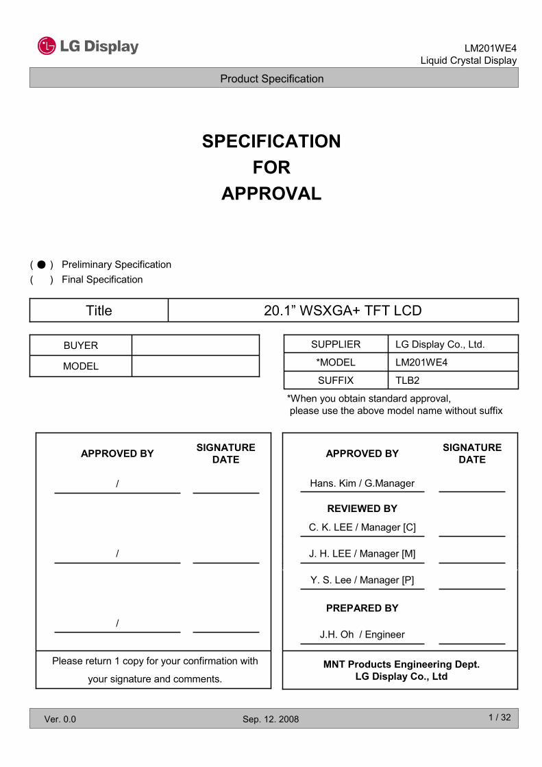
SPECIFICATION
FOR
APPROVAL
20.1” WSXGA+ TFT LCDTitle
MODEL
BUYER
)
)
(
(
Final Specification
Preliminary Specification●
Please return 1 copy for your confirmation with
your signature and comments.
/
/
/
SIGNATURE
DATEAPPROVED BY
*When you obtain standard approval,
please use the above model name without suffix
LM201WE4*MODEL
TLB2SUFFIX
LG Display Co., Ltd.SUPPLIER
J. H. LEE / Manager [M]
C. K. LEE / Manager [C]
MNT Products Engineering Dept.
LG Display Co., Ltd
J.H. Oh / Engineer
PREPARED BY
Y. S. Lee / Manager [P]
REVIEWED BY
Hans. Kim / G.Manager
SIGNATURE
DATEAPPROVED BY

Product Specification
2 / 32
LM201WE4
Liquid Crystal Display
Ver. 0.0 Sep. 12. 2008
Contents
ENVIRONMENT7-3
20VCC POWER DIP CONDITION3-7
31PRECAUTIONS9
18
9INTERFACE CONNECTIONS3-2
COLOR INPUT DATA REFERNECE3-5
30DESIGNATION OF LOT MARK8-1
30PACKING FORM8-2
30PACKING8
29EMC7-2
1COVER
2CONTENTS
3RECORD OF REVISIONS
4GENERAL DESCRIPTION1
5ABSOLUTE MAXIMUM RATINGS2
6ELECTRICAL SPECIFICATIONS3
6ELECTRICAL CHARACTREISTICS3-1
16SIGNAL TIMING SPECIFICATIONS3-3
17SIGNAL TIMING WAVEFORMS3-4
19POWER SEQUENCE3-6
21OPTICAL SFECIFICATIONS4
25MECHANICAL CHARACTERISTICS5
28RELIABILITY6
29INTERNATIONAL STANDARDS7
29SAFETY7-1
PageITEMNo
Product Specification
3 / 32
LM201WE4
Liquid Crystal Display
Ver. 0.0 Sep. 12. 2008
RECORD OF REVISIONS
Preliminary Specification of LM201WE4-TLB2-Sep. 12. 20080.0
DESCRIPTIONPageRevision DateRevision No

Product Specification
4 / 32
LM201WE4
Liquid Crystal Display
Ver. 0.0 Sep. 12. 2008
1. General Description
LM201WE4 is a Color Active Matrix Liquid Crystal Display with an integral Cold Cathode Fluorescent
Lamp(CCFL) backlight system. The matrix employs a-Si Thin Film Transistor as the active element.
It is a transmissive type display operating in the normally White mode. It has a 20.1 inch diagonally
measured active display area with WSXGA+ resolution (1050 vertical by 1680 horizontal pixel array)
Each pixel is divided into Red, Green and Blue sub-pixels or dots which are arranged in vertical stripes.
Gray scale or the brightness of the sub-pixel color is determined with a 8-bit gray scale signal for each dot,
thus, presenting a palette of more than 16,7M colors with A-FRC(Advanced Frame Rate Control).
It has been designed to apply the 8Bit 2 port LVDS interface.
I t i s in tended to suppor t d isp lays where h igh br ightness, super wide v iewing ang le,
high color saturation, and high color are important.
General Features
TFT-LCD Panel(1680 × 1050 pixels)
Source Driver Circuit
Timing ControlBlock
Power Circuit Block
CN1(30pin)
Backlight Assembly(4 CCFL)
RGB, Dclk, DEHsync, Vsync
(LVDS 2 port)
VLCD(+5V)
G1050
G1
S1680S1
Gate Driver circuit
CN2, 3(2PIN)
CN4, 5(2PIN)
VLamp
VLamp
Figure 1. Block diagram
Viewing Angle Free ( R/L 170(Typ.), U/D 160(Typ) )Viewing Angle (CR>10)
16,7 M colorsColor Depth
1680 horiz. By 1050 vert. Pixels RGB strip arrangementPixel Format
300 cd/m2 (Center 1 point, Typ.)Luminance, White
Total 26.98 Watt(Typ.) (4.78 Watt@VLCD, 22.2 Watt@300cd/[LAMP=(7.5mA)])Power Consumption
2,100 g (Typ.)Weight
Transmissive mode, Normally WhiteDisplay Operating Mode
Hard coating(3H) & Anti-Glare treatment of the front polarizerSurface Treatment
0.258mm x 0.258mmPixel Pitch
459.4(H) x 296.4 (V) x 16.5(D) mm (Typ.)Outline Dimension
20.1 inches(511.133mm) diagonal (Aspect ratio 16:10)Active Screen Size
Product Specification
5 / 32
LM201WE4
Liquid Crystal Display
Ver. 0.0 Sep. 12. 2008
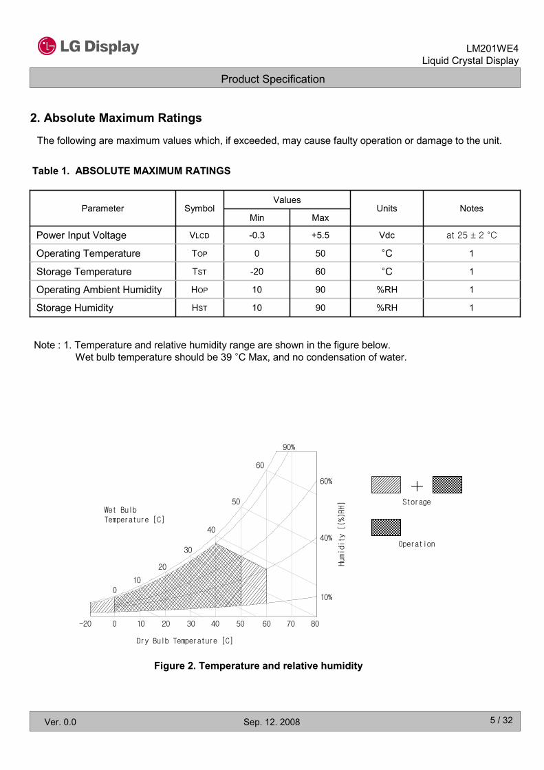
2. Absolute Maximum Ratings
The following are maximum values which, if exceeded, may cause faulty operation or damage to the unit.
Table 1. ABSOLUTE MAXIMUM RATINGS
Note : 1. Temperature and relative humidity range are shown in the figure below.
Wet bulb temperature should be 39 °C Max, and no condensation of water.
Units
1%RH9010HOPOperating Ambient Humidity
1%RH9010HSTStorage Humidity
1°C60-20TSTStorage Temperature
1°C500TOPOperating Temperature
at 25 ± 2 °CVdc+5.5-0.3VLCDPower Input Voltage
MaxMinParameter Notes
ValuesSymbol
90%
10 20 30 40 50 60 70 800-20
010
20
30
40
50
Dry Bulb Temperature [C]
Wet BulbTemperature [C]
Storage
Operation
Humidi
ty [
(%)
RH]
10%
40%
60%
60
Figure 2. Temperature and relative humidity
Product Specification
6 / 32
LM201WE4
Liquid Crystal Display
Ver. 0.0 Sep. 12. 2008
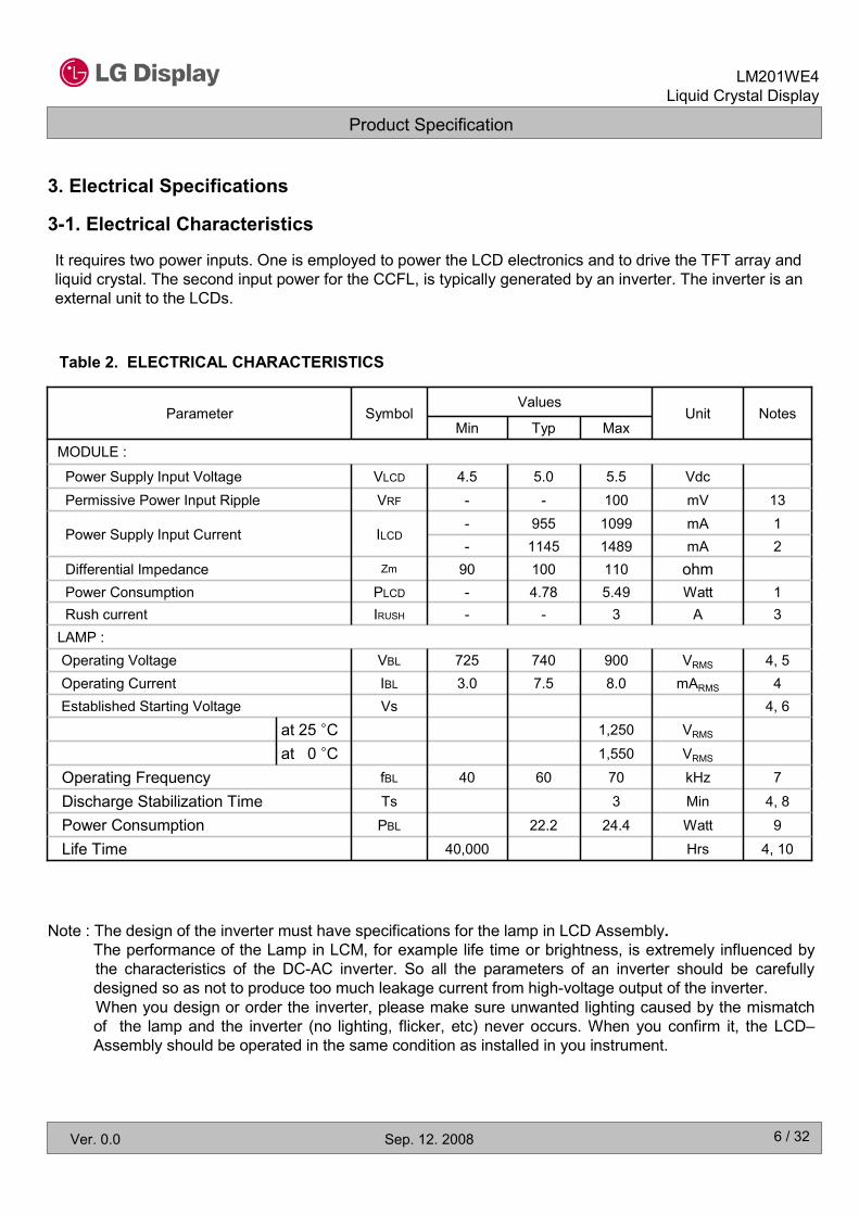
3. Electrical Specifications
3-1. Electrical Characteristics
It requires two power inputs. One is employed to power the LCD electronics and to drive the TFT array and
liquid crystal. The second input power for the CCFL, is typically generated by an inverter. The inverter is an
external unit to the LCDs.
Table 2. ELECTRICAL CHARACTERISTICS
4, 10Hrs40,000Life Time
LAMP :
4, 5VRMS900740725VBLOperating Voltage
4mARMS8.07.53.0IBLOperating Current
4, 6VsEstablished Starting Voltage
VRMS1,250at 25 °C
VRMS1,550at 0 °C
7kHz706040fBLOperating Frequency
4, 8Min3TsDischarge Stabilization Time
9Watt24.422.2PBLPower Consumption
3A3--IRUSHRush current
MODULE :
1Watt5.494.78-PLCDPower Consumption
ohm11010090ZmDifferential Impedance
Vdc5.55.04.5VLCDPower Supply Input Voltage
13mV100--VRFPermissive Power Input Ripple
1mA1099955-
2mA14891145-ILCDPower Supply Input Current
Parameter SymbolMaxTypMin
NotesUnitValues
Note : The design of the inverter must have specifications for the lamp in LCD Assembly.
The performance of the Lamp in LCM, for example life time or brightness, is extremely influenced by
the characteristics of the DC-AC inverter. So all the parameters of an inverter should be carefully
designed so as not to produce too much leakage current from high-voltage output of the inverter.
When you design or order the inverter, please make sure unwanted lighting caused by the mismatch
of the lamp and the inverter (no lighting, flicker, etc) never occurs. When you confirm it, the LCD–
Assembly should be operated in the same condition as installed in you instrument.

Product Specification
7 / 32
LM201WE4
Liquid Crystal Display
Ver. 0.0 Sep. 12. 2008
Note. Do not attach a conducting tape to lamp connecting wire. If the lamp wire attach to a conducting tape,
TFT-LCD Module has a low luminance and the inverter has abnormal action. Because leakage current
is occurred between lamp wire and conducting tape.
1. The specified current and power consumption are under the VLCD=5.0V, 25 ± 2°C,fV=60Hz condition whereas mosaic pattern(8 x 6) is displayed and fV is the frame frequency.
2. The current is specified at the maximum current pattern.
3. The duration of rush current is about 2ms and rising time of power Input is 500us ± 20%.(min.).
4. Specified values are for a single lamp.
5. Operating voltage is measured at 25 ± 2°C. The variance of the voltage is ± 10%.6. The voltage above VS should be applied to the lamps for more than 1 second for start-up.
(Inverter open voltage must be more than lamp starting voltage.)
Otherwise, the lamps may not be turned on. The used lamp current is the lamp typical current.
7. Lamp frequency may produce interface with horizontal synchronous frequency and as a result this may
cause beat on the display. Therefore lamp frequency shall be as away possible from the horizontal
synchronous frequency and from its harmonics in order to prevent interference.
8. Let ’s def ine the br ightness of the lamp after being l ighted for 5 minutes as 100%.
TS is the time required for the brightness of the center of the lamp to be not less than 95%.
9. The lamp power consumption shown above does not include loss of external inverter.
The used lamp current is the lamp typical current. (PBL = VBL x IBL x NLamp )
10. The life is determined as the time at which brightness of the lamp is 50% compared to that of initial
value at the typical lamp current on condition of continuous operating at 25 ± 2°C.11. The output of the inverter must have symmetrical (negative and positive) voltage waveform and
symmetrical current waveform (Unsymmetrical ratio is less than 10%). Please do not use the inverter
which has unsymmetrical voltage and unsymmetrical current and spike wave.
Requirements for a system inverter design, which is intended to have a better display performance,
a better power efficiency and a more reliable lamp, are following.
It shall help increase the lamp lifetime and reduce leakage current.
a. The asymmetry rate of the inverter waveform should be less than 10%.
b. The distortion rate of the waveform should be within √2 ±10%. * Inverter output waveform had better be more similar to ideal sine wave.
I p
I -p
* Asymmetry rate:
| I p – I –p | / Irms x 100%
* Distortion rate
I p (or I –p) / Irms
12. The inverter which is combined with this LCM, is highly recommended to connect coupling(ballast)
condenser at the high voltage output side. When you use the inverter which has not coupling(ballast)
condenser, it may cause abnormal lamp lighting because of biased mercury as time goes.
13. Permissive power ripple should be measured under VLCD =5.0V, 25°C, fV(frame frequency)=MAXcondition and At that time, we recommend the bandwidth configuration of oscilloscope is to be under
20Mhz. See the figure 3.
14. In case of edgy type back light with over 4 parallel lamps, input current and voltage wave form should
be synchronized

Product Specification
8 / 32
LM201WE4
Liquid Crystal Display
Ver. 0.0 Sep. 12. 2008
White pattern Black pattern
• Permissive Power input ripple (VLCD =5.0V, 25°C, fV(frame frequency)=MAX condition)
• Power consumption (VLCD =5.0V, 25°C, fV (frame frequency=60Hz condition)
[ Figure 3 ] Mosaic pattern & Black Pattern for power consumption measurement
Typical power Pattern Max power Pattern
Product Specification
9 / 32
LM201WE4
Liquid Crystal Display
Ver. 0.0 Sep. 12. 2008
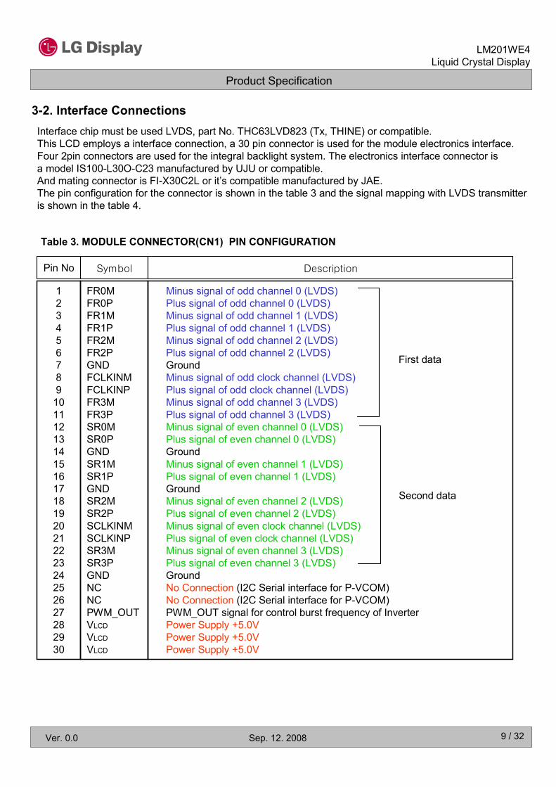
3-2. Interface Connections
Table 3. MODULE CONNECTOR(CN1) PIN CONFIGURATION
1
2
3
4
5
6
7
8
9
10
11
12
13
14
15
16
17
18
19
20
21
22
23
24
25
26
27
28
29
30
Pin No Symbol Description
FR0M
FR0P
FR1M
FR1P
FR2M
FR2P
GND
FCLKINM
FCLKINP
FR3M
FR3P
SR0M
SR0P
GND
SR1M
SR1P
GND
SR2M
SR2P
SCLKINM
SCLKINP
SR3M
SR3P
GND
NC
NC
PWM_OUT
VLCD
VLCD
VLCD
Minus signal of odd channel 0 (LVDS)
Plus signal of odd channel 0 (LVDS)
Minus signal of odd channel 1 (LVDS)
Plus signal of odd channel 1 (LVDS)
Minus signal of odd channel 2 (LVDS)
Plus signal of odd channel 2 (LVDS)
Ground
Minus signal of odd clock channel (LVDS)
Plus signal of odd clock channel (LVDS)
Minus signal of odd channel 3 (LVDS)
Plus signal of odd channel 3 (LVDS)
Minus signal of even channel 0 (LVDS)
Plus signal of even channel 0 (LVDS)
Ground
Minus signal of even channel 1 (LVDS)
Plus signal of even channel 1 (LVDS)
Ground
Minus signal of even channel 2 (LVDS)
Plus signal of even channel 2 (LVDS)
Minus signal of even clock channel (LVDS)
Plus signal of even clock channel (LVDS)
Minus signal of even channel 3 (LVDS)
Plus signal of even channel 3 (LVDS)
Ground
No Connection (I2C Serial interface for P-VCOM)
No Connection (I2C Serial interface for P-VCOM)
PWM_OUT signal for control burst frequency of Inverter
Power Supply +5.0V
Power Supply +5.0V
Power Supply +5.0V
Second data
First data
Interface chip must be used LVDS, part No. THC63LVD823 (Tx, THINE) or compatible.
This LCD employs a interface connection, a 30 pin connector is used for the module electronics interface.
Four 2pin connectors are used for the integral backlight system. The electronics interface connector is
a model IS100-L30O-C23 manufactured by UJU or compatible.
And mating connector is FI-X30C2L or it’s compatible manufactured by JAE.
The pin configuration for the connector is shown in the table 3 and the signal mapping with LVDS transmitter
is shown in the table 4.
Product Specification
10 / 32
LM201WE4
Liquid Crystal Display
Ver. 0.0 Sep. 12. 2008
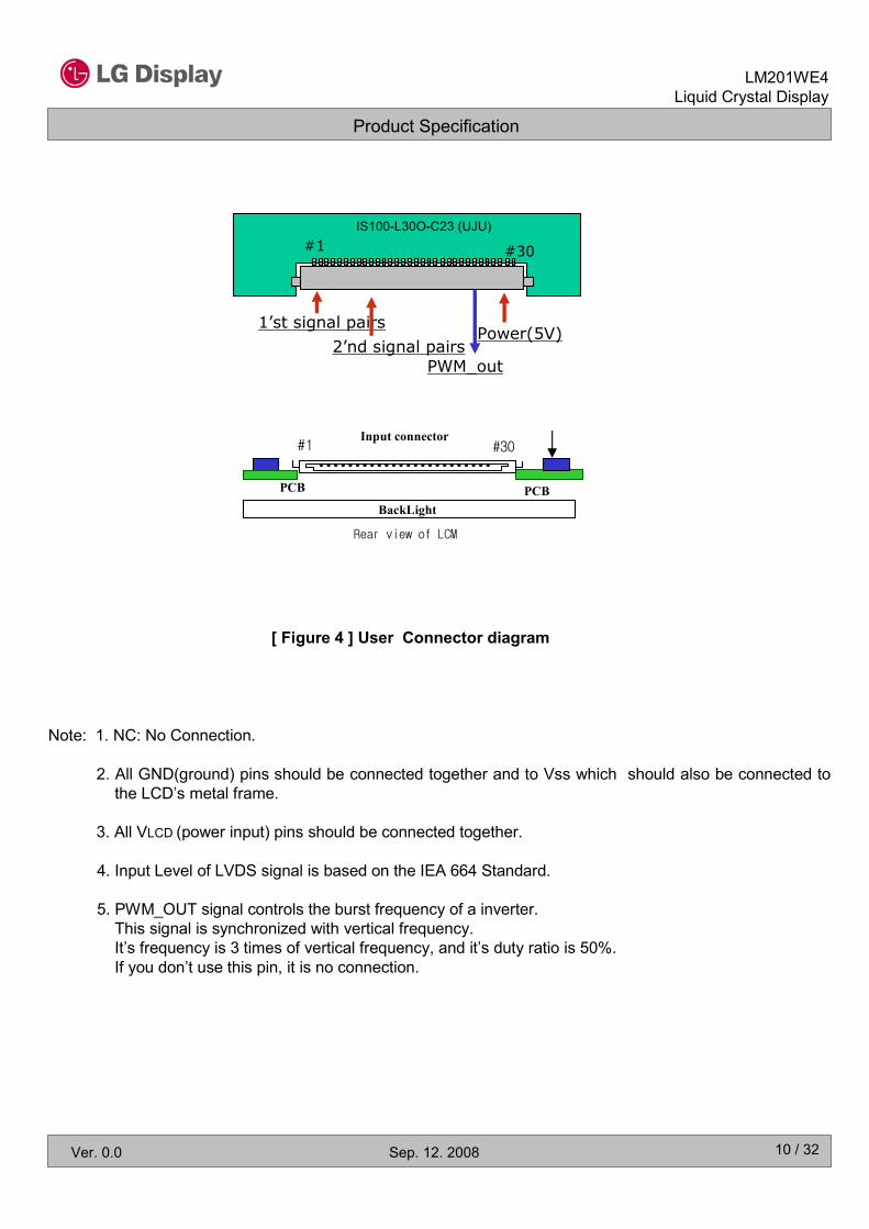
Note: 1. NC: No Connection.
2. All GND(ground) pins should be connected together and to Vss which should also be connected to
the LCD’s metal frame.
3. All VLCD (power input) pins should be connected together.
4. Input Level of LVDS signal is based on the IEA 664 Standard.
5. PWM_OUT signal controls the burst frequency of a inverter.
This signal is synchronized with vertical frequency.
It’s frequency is 3 times of vertical frequency, and it’s duty ratio is 50%.
If you don’t use this pin, it is no connection.
[ Figure 4 ] User Connector diagram
IS100-L30O-C23 (UJU)
#1 #30
1’st signal pairs
2’nd signal pairsPower(5V)
PWM_out
Rear view of LCM
#1 #30Input connector
PCB
BackLight
PCB

Product Specification
11 / 32
LM201WE4
Liquid Crystal Display
Ver. 0.0 Sep. 12. 2008
Table 4. REQUIRED SIGNAL ASSIGNMENT FOR Flat Link (TI:SN75LVDS83) Transmitter
Notes : 1. Refer to LVDS Transmitter Data Sheet for detail descriptions.
2. 7 means MSB and 0 means LSB at R,G,B pixel data
Pin # Require SignalPin Name Pin # Require SignalPin Name
1 Power Supply for TTL InputVCC 29 Ground pin for TTLGND
2 TTL Input (R7)D5 30 TTL Input (DE)D26
3 TTL Input (R5)D6 31 TTL Level clock InputTX CLKIN
4 TTL Input (G0)D7 32 Power Down InputPWR DWN
5 Ground pin for TTLGND 33 Ground pin for PLLPLL GND
6 TTL Input (G1)D8 34 Power Supply for PLLPLL VCC
7 TTL Input (G2)D9 35 Ground pin for PLLPLL GND
8 TTL Input (G6)D10 36 Ground pin for LVDSLVDS GND
9 Power Supply for TTL InputVCC 37 Positive LVDS differential data output 3TxOUT3+
10 TTL Input (G7)D11 38 Negative LVDS differential data output 3TxOUT3-
11 TTL Input (G3)D12 39 Positive LVDS differential clock outputTX CLKOUT+
12 TTL Input (G4)D13 40 Negative LVDS differential clock outputTX CLKOUT-
13 Ground pin for TTLGND 41 Positive LVDS differential data output 2TX OUT2+
14 TTL Input (G5)D14 42 Negative LVDS differential data output 2TX OUT2-
15 TTL Input (B0)D15 43 Ground pin for LVDSLVDS GND
16 TTL Input (B6)D16 44 Power Supply for LVDSLVDS VCC
17 Power Supply for TTL InputVCC 45 Positive LVDS differential data output 1TX OUT1+
46 Negative LVDS differential data output 1TX OUT1-18 TTL Input (B7)D17
47 Positive LVDS differential data output 0TX OUT0+
48 Negative LVDS differential data output 0TX OUT0-
19 TTL Input (B1)D18
20 TTL Input (B2)D19
49 Ground pin for LVDSLVDS GND21 Ground pin for TTL InputGND
22 TTL Input (B3)D20
23 TTL Input (B4)D21
50 TTL Input (R6)D27
51 TTL Input (R0)D0
24 TTL Input (B5)D22
25 TTL Input (RSVD)D23
52 TTL Input (R1)D1
53 Ground pin for TTLGND
26 Power Supply for TTL InputVCC 54 TTL Input (R2)D2
55 TTL Input (R3)D327 TTL Input (HSYNC)D24
56 TTL Input (R4)D428 TTL Input (VSYNC)D25

Product Specification
12 / 32
LM201WE4
Liquid Crystal Display
Ver. 0.0 Sep. 12. 2008
LVDS Input characteristics
NotesUnitMaxMinSymbolDescription
85MHz > Fclk ≥ 65MHzps+ 400- 400tSKEWLVDS Clock to Data Skew Margin
-
-
-
65MHz > Fclk ≥ 25MHz
%± 3-FDEVMaximum deviation
of input clock frequency during SSC
KHz200-FMOD
Maximum modulation frequency
of input clock during SSC
- 1/7
- 600
Tclk+ 1/7tSKEW_EOLVDS Clock to Clock Skew Margin (Even to Odd)
ps+ 600tSKEW
-V2.10.3VINLVDS Input Voltage Range
-V1.80.6VCMLVDS Common mode Voltage
-mV600100|VID|LVDS Differential Voltage
NotesUnitMaxMinSymbolDescription
1. DC Specification
2. AC Specification

Product Specification
13 / 32
LM201WE4
Liquid Crystal Display
Ver. 0.0 Sep. 12. 2008
< Clock skew margin between channel >
< LVDS Data Format >
3. Data Format
1) LVDS 2 Port
< Spread Spectrum >
Time
Fcenter
Fmax
Fmin
FMOD
1
Fcenter * FDEV
Freq.
Product Specification
14 / 32
LM201WE4
Liquid Crystal Display
Ver. 0.0 Sep. 12. 2008
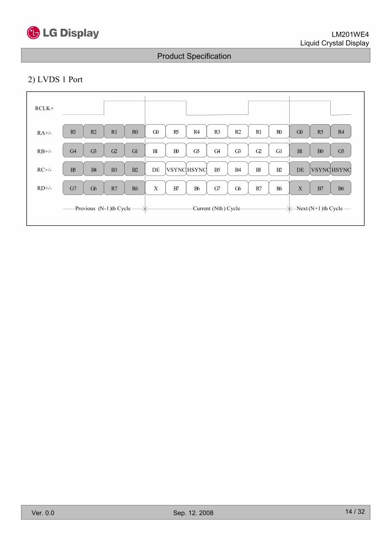
2) LVDS 1 Port
G0 R5 R4 R3 R2 R1 R0
B1 B0 G5 G4 G3 G2 G1
DE VSYNC HSYNC B5 B4 B3 B2
X B7 B6 G7 G6 R7 R6
R1 R0
G2 G1
B3 B2
R7 R6
G0
B1
DE
X
Current (Nth ) Cycle
R5 R4
B0 G5
VSYNC HSYNC
B7 B6
R3 R2
G4 G3
B5 B4
G7 G6
Previous (N-1)th Cycle Next (N+1)th Cycle
RCLK+
RA+/-
RB+/-
RC+/-
RD+/-
Product Specification
15 / 32
LM201WE4
Liquid Crystal Display
Ver. 0.0 Sep. 12. 2008
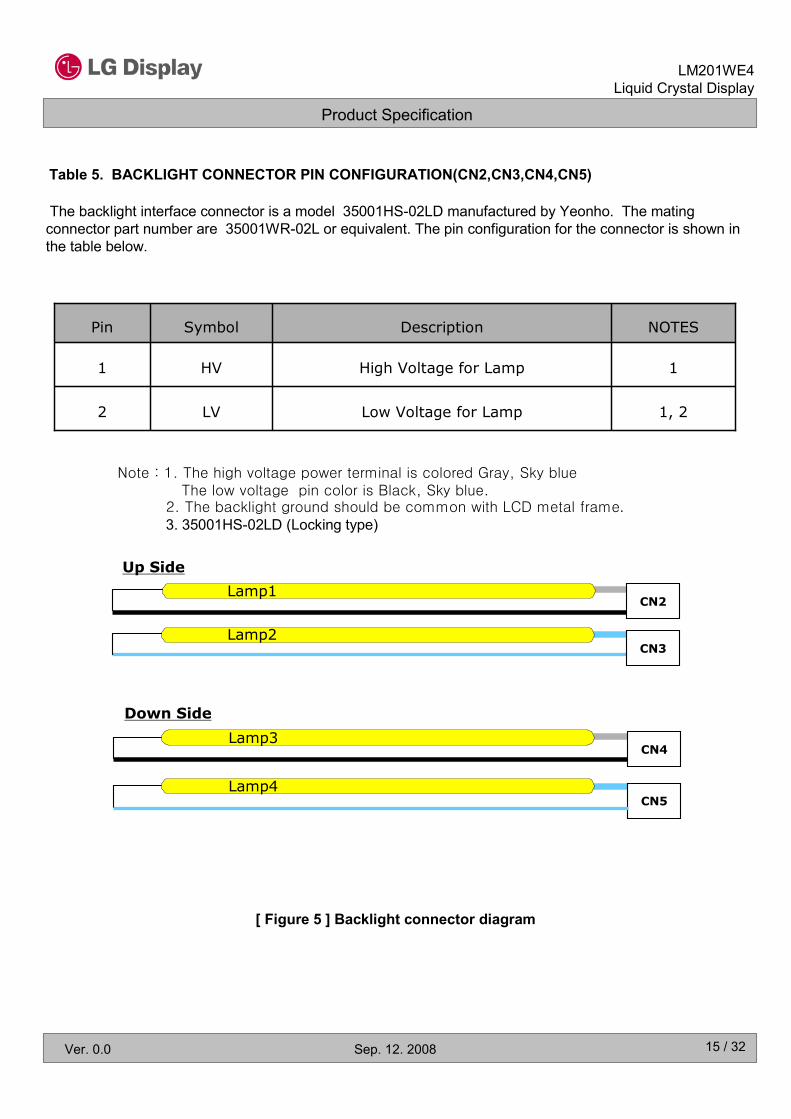
Table 5. BACKLIGHT CONNECTOR PIN CONFIGURATION(CN2,CN3,CN4,CN5)
The backlight interface connector is a model 35001HS-02LD manufactured by Yeonho. The mating
connector part number are 35001WR-02L or equivalent. The pin configuration for the connector is shown in
the table below.
1, 2
1
NOTES
Low Voltage for Lamp
High Voltage for Lamp
Description
LV
HV
Symbol
2
1
Pin
[ Figure 5 ] Backlight connector diagram
Note : 1. The high voltage power terminal is colored Gray, Sky blueThe low voltage pin color is Black, Sky blue.
2. The backlight ground should be common with LCD metal frame.3. 35001HS-02LD (Locking type)
Up Side
Down Side
CN2
CN3
CN4
CN5
Lamp1
Lamp2
Lamp3
Lamp4

Product Specification
16 / 32
LM201WE4
Liquid Crystal Display
Ver. 0.0 Sep. 12. 2008
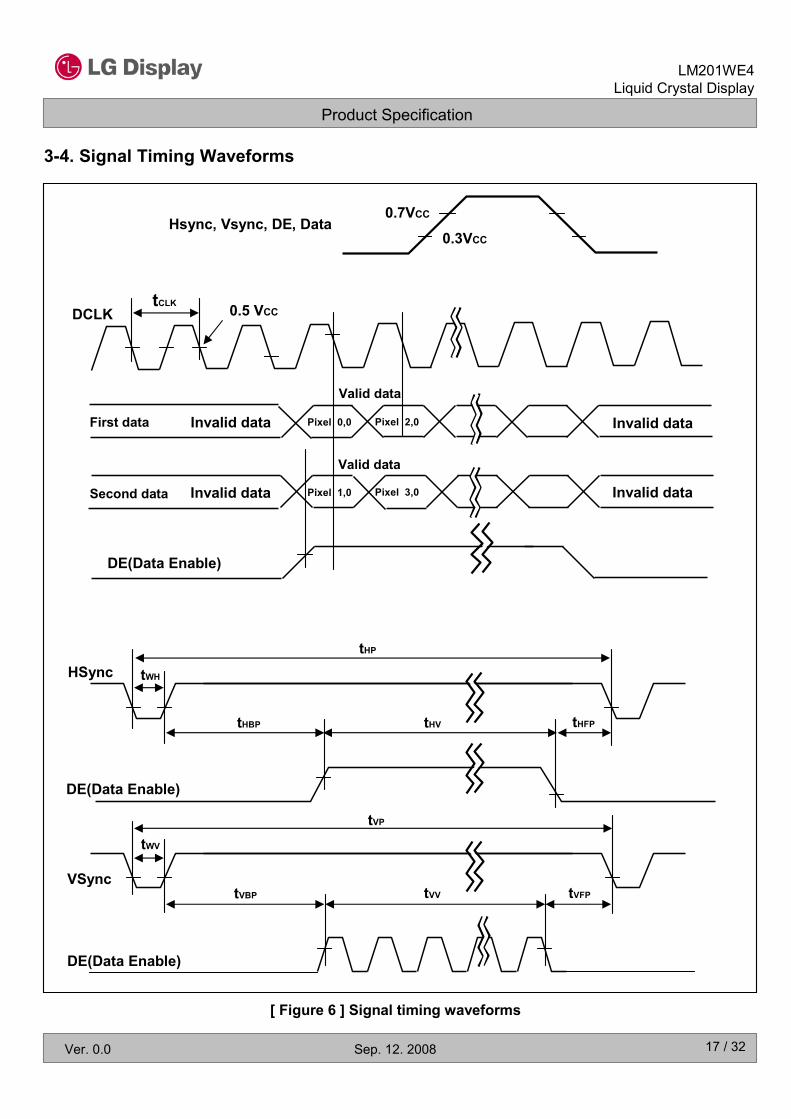
Notes: Hsync period and Hsync width-active should be even number times of tCLK. If the value is odd number
times of tCLK, display control signal can be asynchronous. In order to operate this LCM a Hsync,
Vsync, and DE(data enable) signals should be used.
1. The performance of the electro-optical characteristics may be influenced by variance of the vertical
refresh rates.
2. Vsync and Hsync should be keep the above specification.
3. Hsync Period, Hsync Width, and Horizontal Back Porch should be any times of character
number(8).
4. The polarity of Hsync, Vsync is not restricted.
3-3. Signal Timing Specifications
Table 6. Timing Table
This is the signal timing required at the input of the User connector. All of the interface signal timing should be
satisfied with the following specifications for it’s proper operation.
tCLK64168tWHWidth
tHP
KHz
2503010-Vertical Blank
3608040-Horizontal Blank
tHP
39215tVBPVertical Back Porch
tCLK
2004016tHBPHorizontal Back Porch
962416tHFPHorizontal Front Porch
105010501050tVVVertical Valid
632tVFPVertical Front Porch
Hz776048fVFrequency
20563tWVWidth
81.52264.67451.495fHFrequency
tCLK1200920880tHPPeriod
Hsync
tHP130010801060tVPPeriod
Vsync
840840840tHVHorizontal Valid
DE
(Data
Enable)
MHz8259.547.375-Frequency
Pixel frequency
: Typ. 119MHz
(2pixel/clk)
ns21.116.812.19tCLKPeriod
DCLK
NoteUnitMaxTypMinSymbolITEM
Product Specification
17 / 32
LM201WE4
Liquid Crystal Display
Ver. 0.0 Sep. 12. 2008
3-4. Signal Timing Waveforms
0.7VCC
0.3VCC
tCLK
Invalid data
Valid data
Invalid data
Invalid data
Invalid data
Pixel 0,0 Pixel 2,0
Pixel 1,0 Pixel 3,0
DE(Data Enable)
Valid data
0.5 VCC
tHP
tHBP tHV tHFP
tVP
tWV
tVBP tVV tVFP
HSync
VSync
DE(Data Enable)
DE(Data Enable)
DCLK
First data
Second data
Hsync, Vsync, DE, Data
tWH
[ Figure 6 ] Signal timing waveforms
Product Specification
18 / 32
LM201WE4
Liquid Crystal Display
Ver. 0.0 Sep. 12. 2008
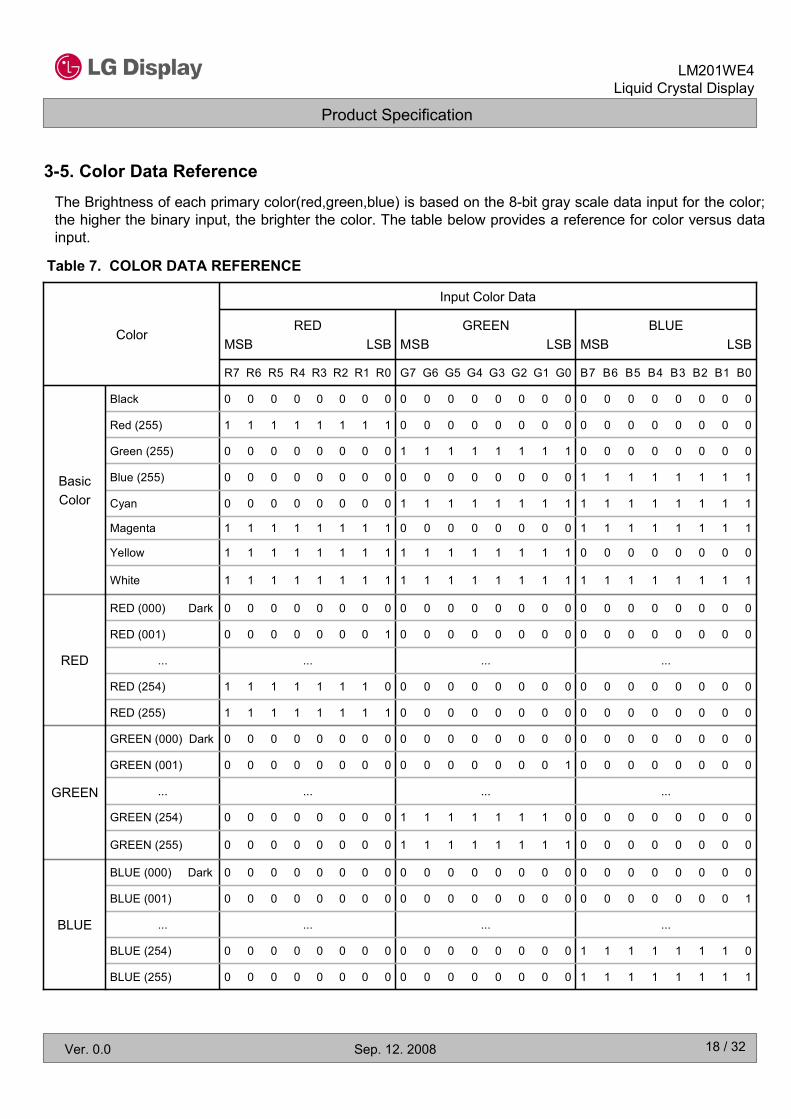
3-5. Color Data Reference
The Brightness of each primary color(red,green,blue) is based on the 8-bit gray scale data input for the color;
the higher the binary input, the brighter the color. The table below provides a reference for color versus data
input.
Table 7. COLOR DATA REFERENCE
0 0 0 0 0 0 0 00 0 0 0 0 0 0 00 0 0 0 0 0 0 0GREEN (000) Dark
GREEN
0 0 0 0 0 0 0 00 0 0 0 0 0 0 10 0 0 0 0 0 0 0GREEN (001)
............
0 0 0 0 0 0 0 01 1 1 1 1 1 1 00 0 0 0 0 0 0 0GREEN (254)
0 0 0 0 0 0 0 01 1 1 1 1 1 1 10 0 0 0 0 0 0 0GREEN (255)
0 0 0 0 0 0 0 00 0 0 0 0 0 0 00 0 0 0 0 0 0 0RED (000) Dark
RED
0 0 0 0 0 0 0 00 0 0 0 0 0 0 00 0 0 0 0 0 0 1RED (001)
............
0 0 0 0 0 0 0 00 0 0 0 0 0 0 01 1 1 1 1 1 1 0RED (254)
0 0 0 0 0 0 0 00 0 0 0 0 0 0 01 1 1 1 1 1 1 1RED (255)
0 0 0 0 0 0 0 10 0 0 0 0 0 0 00 0 0 0 0 0 0 0BLUE (001)
............
1 1 1 1 1 1 1 00 0 0 0 0 0 0 00 0 0 0 0 0 0 0BLUE (254)
1 1 1 1 1 1 1 10 0 0 0 0 0 0 00 0 0 0 0 0 0 0BLUE (255)
BLUE (000) Dark
White
Yellow
Magenta
Cyan
Blue (255)
Green (255)
Red (255)
Black 0 0 0 0 0 0 0 00 0 0 0 0 0 0 00 0 0 0 0 0 0 0
Basic
Color
0 0 0 0 0 0 0 00 0 0 0 0 0 0 01 1 1 1 1 1 1 1
0 0 0 0 0 0 0 01 1 1 1 1 1 1 10 0 0 0 0 0 0 0
1 1 1 1 1 1 1 10 0 0 0 0 0 0 00 0 0 0 0 0 0 0
1 1 1 1 1 1 1 11 1 1 1 1 1 1 10 0 0 0 0 0 0 0
1 1 1 1 1 1 1 10 0 0 0 0 0 0 01 1 1 1 1 1 1 1
0 0 0 0 0 0 0 01 1 1 1 1 1 1 11 1 1 1 1 1 1 1
1 1 1 1 1 1 1 11 1 1 1 1 1 1 11 1 1 1 1 1 1 1
BLUE
MSB LSB
GREEN
MSB LSB
RED
MSB LSB
B7 B6 B5 B4 B3 B2 B1 B0G7 G6 G5 G4 G3 G2 G1 G0R7 R6 R5 R4 R3 R2 R1 R0
0 0 0 0 0 0 0 00 0 0 0 0 0 0 00 0 0 0 0 0 0 0
BLUE
Color
Input Color Data

Product Specification
19 / 32
LM201WE4
Liquid Crystal Display
Ver. 0.0 Sep. 12. 2008
3-6. Power Sequence
Interface Signal, Vi
(Digital RGB signal,
SCDT ,Vsync, Hsync,
DE, Clock to PanelLink
Transmitter)
Power Supply for
Backlight Inverter
Power Supply, VLCD
Notes : 1. Please avoid floating state of interface signal at invalid period.
2. When the interface signal is invalid, be sure to pull down the power supply for LCD VLCD to 0V.
3. Lamp power must be turn on after power supply for LCD an interface signal are valid.
ms50-0.01T5
ms1000-0.01T6
s--1T7
ms50-0.01T2
ms
ms--200T3
--200T4
ms10-0.5T1
MaxTypMinUnits
ValuesParameter
Table 8. POWER SEQUENCE
[ Figure 7 ] Power sequence
10%
90% 90%
10%
T1 T2 T5 T7
T3 T4
Valid data
Lamp on
0V
OFF OFF
T6

Product Specification
20 / 32
LM201WE4
Liquid Crystal Display
Ver. 0.0 Sep. 12. 2008
3-6. VLCD Power Dip Condition
1) Dip condition
3.5V ≤VLCD< 4.5V , td≤20ms
2) VLCD< 3.5V
VLCD-dip conditions should also follow the Power On/Off conditions for supply voltage.
4.5V
3.5V
VLCD
td
[ Figure 8 ] Power dip condition
Product Specification
21 / 32
LM201WE4
Liquid Crystal Display
Ver. 0.0 Sep. 12. 2008
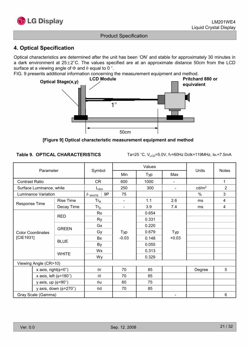
4. Optical Specification
Optical characteristics are determined after the unit has been ‘ON’ and stable for approximately 30 minutes in
a dark environment at 25±2°C. The values specified are at an approximate distance 50cm from the LCD
surface at a viewing angle of Φ and θ equal to 0 °.FIG. 9 presents additional information concerning the measurement equipment and method.
LCD ModuleOptical Stage(x,y)
Pritchard 880 or
equivalent
50cm
[Figure 9] Optical characteristic measurement equipment and method
Table 9. OPTICAL CHARACTERISTICS Ta=25 °C, VLCD=5.0V, fV=60Hz Dclk=119MHz, IBL=7.5mA
y axis, down (φ=270°)
y axis, up (φ=90°)
x axis, left (φ=180°)
x axis, right(φ=0°)
Viewing Angle (CR>10)
5Degree8570θr
8570θl
7560θu
8570θd
6-Gray Scale (Gamma)
9P
WHITE
BLUE
GREEN
RED
0.679Gy
0.220Gx
0.055By
0.148Bx
0.329Wy
0.313Wx
Decay Time
Rise Time
4ms7.43.9-TrD
0.331Ry
Typ
+0.03
0.654
Typ
-0.03
Rx
Color Coordinates
[CIE1931]
4ms2.61.1-TrRResponse Time
3%75δ WHITELuminance Variation
2cd/m2-300250LWHSurface Luminance, white
1
NotesUnits
-1000600CRContrast Ratio
MaxTypMin
ValuesSymbolParameter

Product Specification
22 / 32
LM201WE4
Liquid Crystal Display
Ver. 0.0 Sep. 12. 2008
Notes 1. Contrast Ratio(CR) is defined mathematically as :
Surface Luminance with all white pixelsContrast Ratio =
Surface Luminance with all black pixels
2. Surface luminance is luminance value at No.1 point across the LCD surface 50cmfrom the surface with all pixels displaying white. For more information see FIG 10.
3. The variation in surface luminance , δ WHITE is defined as :
Measuring point for surface luminance & measuring point for luminance variation
(%)100)L .... ,L ,(L Maximum
)L .. ,L,Minimum(L
on9on2on1
on9on2on1 ×…
=WHITEδ
1
H
A
B
V
Active AreaA : H/4 mm
B : V/4 mm
@ H,V : Active Area
H/10
V/10
2 3 4
7 8 9
5 6
[ FIG. 10 ] Measure Point for Luminance
Product Specification
23 / 32
LM201WE4
Liquid Crystal Display
Ver. 0.0 Sep. 12. 2008
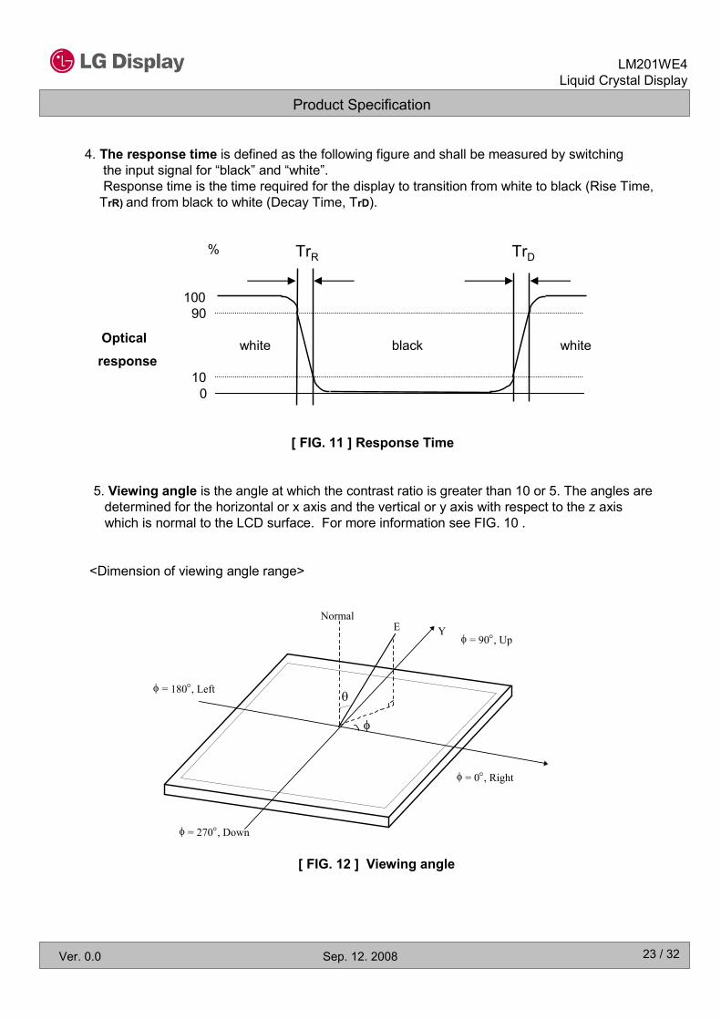
4. The response time is defined as the following figure and shall be measured by switching
the input signal for “black” and “white”.
Response time is the time required for the display to transition from white to black (Rise Time,
TrR) and from black to white (Decay Time, TrD).
100
90
10
0
%
Optical
responsewhite black white
TrR TrD
5. Viewing angle is the angle at which the contrast ratio is greater than 10 or 5. The angles are
determined for the horizontal or x axis and the vertical or y axis with respect to the z axis
which is normal to the LCD surface. For more information see FIG. 10 .
<Dimension of viewing angle range>
Normal
Y E
φ
θ
φ = 0°, Right
φ = 180°, Left
φ = 270°, Down
φ = 90°, Up
[ FIG. 11 ] Response Time
[ FIG. 12 ] Viewing angle
Product Specification
24 / 32
LM201WE4
Liquid Crystal Display
Ver. 0.0 Sep. 12. 2008
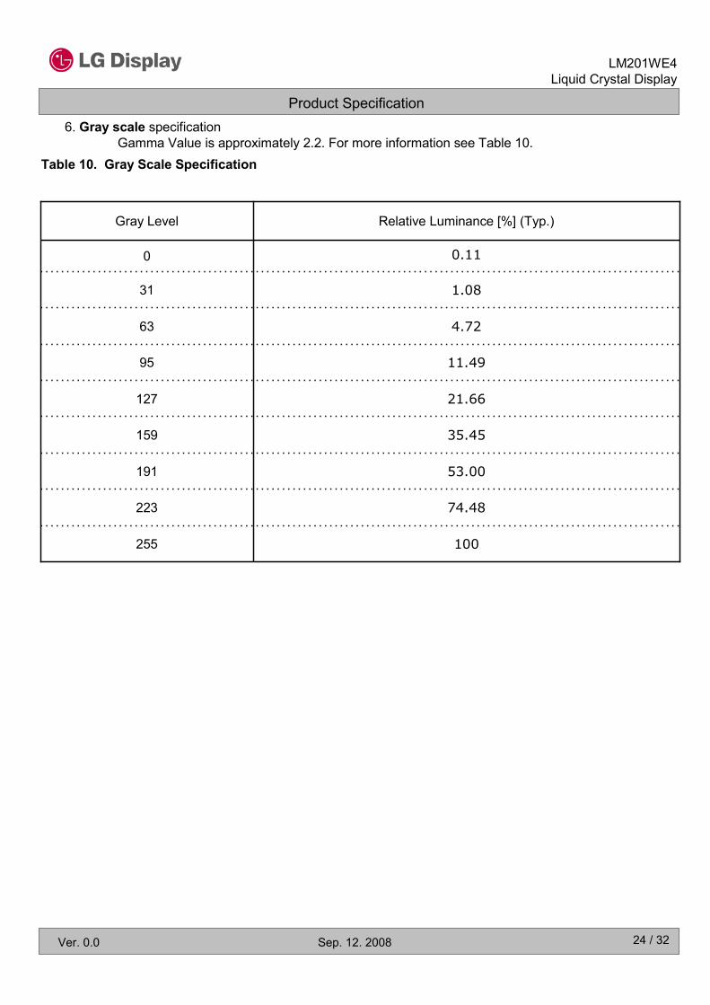
Table 10. Gray Scale Specification
6. Gray scale specification
Gamma Value is approximately 2.2. For more information see Table 10.
0.110
100
74.48
53.00
35.45
21.66
11.49
4.72
1.08
255
223
191
159
127
95
63
31
Relative Luminance [%] (Typ.)Gray Level
Product Specification
25 / 32
LM201WE4
Liquid Crystal Display
Ver. 0.0 Sep. 12. 2008
5. Mechanical Characteristics
The contents provide general mechanical characteristics. In addition the figures in the next page are detailed
mechanical drawing of the LCD.
Notes : Please refer to a mechanic drawing in terms of tolerance at the next page.
270.90mmVertical
Hard coating(3H)
Anti-Glare treatment of the front polarizerSurface Treatment
2,100 g (Typ.), 2,200 g (Max.)Weight
275.9mmVertical
296.4mmVertical
16.5mmDepth
433.44mmHorizontalActive Display Area
438.4mmHorizontalBezel Area
459.4mmHorizontal
Outline Dimension

Product Specification
26 / 32
LM201WE4
Liquid Crystal Display
Ver. 0.0 Sep. 12. 2008
<FRONT VIEW>

Product Specification
27 / 32
LM201WE4
Liquid Crystal Display
Ver. 0.0 Sep. 12. 2008
<REAR VIEW>
Product Specification
28 / 32
LM201WE4
Liquid Crystal Display
Ver. 0.0 Sep. 12. 2008
6. Reliability
Environment test condition
Wave form : random
Vibration level : 1.0G RMS
Bandwidth : 10-300Hz
Duration : X,Y,Z, 30 min
One time each direction
Vibration test
(non-operating)5
0 - 10,000 feet(3048m)
0 - 40,000 feet(12,192m)
Altitude
operating
storage / shipment
7
Shock level : 120G
Waveform : half sine wave, 2ms
Direction :±X, ±Y, ±ZOne time each direction
Shock test
(non-operating)6
Ta= 0°C 240hLow temperature operation test4
Ta= 50°C 50%RH 240hHigh temperature operation test3
Ta= -20°C 240hLow temperature storage test2
Ta= 60°C 240hHigh temperature storage test1
No Test Item Condition

Product Specification
29 / 32
LM201WE4
Liquid Crystal Display
Ver. 0.0 Sep. 12. 2008
7. International Standards
7-2. EMC
a) ANSI C63.4 “Methods of Measurement of Radio-Noise Emissions from Low-Voltage Electrical and
Electrical Equipment in the Range of 9kHZ to 40GHz. “American National Standards Institute(ANSI),
1992
b) C.I.S.P.R “Limits and Methods of Measurement of Radio Interface Characteristics of Information
Technology Equipment.“ International Special Committee on Radio Interference.
c) EN 55022 “Limits and Methods of Measurement of Radio Interface Characteristics of Information
Technology Equipment.“ European Committee for Electrotechnical Standardization.(CENELEC), 1998
( Including A1: 2000 )
7-1. Safety
a) UL 60950-1:2003, First Edition, Underwriters Laboratories, Inc.,
Standard for Safety of Information Technology Equipment.
b) CAN/CSA C22.2, No. 60950-1-03 1st Ed. April 1, 2003, Canadian Standards Association,
Standard for Safety of Information Technology Equipment.
c) EN 60950-1:2001, First Edition,
European Committee for Electrotechnical Standardization(CENELEC)
European Standard for Safety of Information Technology Equipment.
7-3. Environment
a) RoHS, Directive 2002/95/EC of the European Parliament and of the Council on the reduction of
the use of certain hazardous substances in electrical and electronic equipment, January 2003.
Product Specification
30 / 32
LM201WE4
Liquid Crystal Display
Ver. 0.0 Sep. 12. 2008
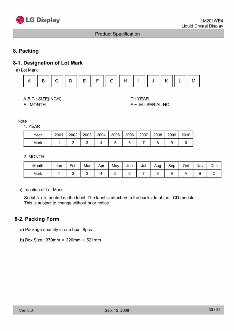
8. Packing
8-1. Designation of Lot Mark
a) Lot Mark
A B C D E F G H I J K L M
A,B,C : SIZE(INCH) D : YEAR
E : MONTH F ~ M : SERIAL NO.
Note
1. YEAR
2. MONTH
Mark
Year
0
2010
6
2006
7
2007
8
2008
9
2009
4
2004
5
2005
321
200320022001
B
Nov
Mark
Month
A
Oct
6
Jun
7
Jul
8
Aug
9
Sep
4
Apr
5
May
C321
DecMarFebJan
b) Location of Lot Mark
Serial No. is printed on the label. The label is attached to the backside of the LCD module.
This is subject to change without prior notice.
8-2. Packing Form
a) Package quantity in one box : 8pcs
b) Box Size : 370mm × 320mm × 521mm
Product Specification
31 / 32
LM201WE4
Liquid Crystal Display
Ver. 0.0 Sep. 12. 2008
9. PRECAUTIONS
Please pay attention to the followings when you use this TFT LCD module.
9-1. MOUNTING PRECAUTIONS
(1) You must mount a module using holes arranged in four corners or four sides.
(2) You should consider the mounting structure so that uneven force (ex. Twisted stress) is not applied to the
module. And the case on which a module is mounted should have sufficient strength so that external
force is not transmitted directly to the module.
(3) Please attach the surface transparent protective plate to the surface in order to protect the polarizer.
Transparent protective plate should have sufficient strength in order to the resist external force.
(4) You should adopt radiation structure to satisfy the temperature specification.
(5) Acetic acid type and chlorine type materials for the cover case are not desirable because the former
generates corrosive gas of attacking the polarizer at high temperature and the latter causes circuit break
by electro-chemical reaction.
(6) Do not touch, push or rub the exposed polarizers with glass, tweezers or anything harder than HB
pencil lead. And please do not rub with dust clothes with chemical treatment.
Do not touch the surface of polarizer for bare hand or greasy cloth.(Some cosmetics are detrimental
to the polarizer.)
(7) When the surface becomes dusty, please wipe gently with absorbent cotton or other soft materials like
chamois soaks with petroleum benzene. Normal-hexane is recommended for cleaning the adhesives
used to attach front / rear polarizers. Do not use acetone, toluene and alcohol because they cause
chemical damage to the polarizer.
(8) Wipe off saliva or water drops as soon as possible. Their long time contact with polarizer causes
deformations and color fading.
(9) Do not open the case because inside circuits do not have sufficient strength.
9-2. OPERATING PRECAUTIONS
(1) The spike noise causes the mis-operation of circuits. It should be lower than following voltage :
V=±200mV(Over and under shoot voltage)(2) Response time depends on the temperature.(In lower temperature, it becomes longer.)
(3) Brightness depends on the temperature. (In lower temperature, it becomes lower.)
And in lower temperature, response time(required time that brightness is stable after turned on) becomes
longer.
(4) Be careful for condensation at sudden temperature change. Condensation makes damage to polarizer or
electrical contacted parts. And after fading condensation, smear or spot will occur.
(5) When fixed patterns are displayed for a long time, remnant image is likely to occur.
(6) Module has high frequency circuits. Sufficient suppression to the electromagnetic interference shall be
done by system manufacturers. Grounding and shielding methods may be important to minimized the
interference.
(7) Please do not give any mechanical and/or acoustical impact to LCM. Otherwise, LCM can not be
operated its full characteristics perfectly.
(8) A screw which is fastened up the steels should be a machine screw (if not, it causes metallic foreign
material and deal LCM a fatal blow)
(9) Please do not set LCD on its edge.
Product Specification
32 / 32
LM201WE4
Liquid Crystal Display
Ver. 0.0 Sep. 12. 2008
Since a module is composed of electronic circuits, it is not strong to electrostatic discharge. Make certain that
treatment persons are connected to ground through wrist band etc. And don’t touch interface pin directly.
9-3. ELECTROSTATIC DISCHARGE CONTROL
Strong light exposure causes degradation of polarizer and color filter.
9-4. PRECAUTIONS FOR STRONG LIGHT EXPOSURE
When storing modules as spares for a long time, the following precautions are necessary.
(1) Store them in a dark place. Do not expose the module to sunlight or fluorescent light. Keep the
temperature between 5°C and 35°C at normal humidity.(2) The polarizer surface should not come in contact with any other object.
It is recommended that they be stored in the container in which they were shipped.
9-5. STORAGE
9-6. HANDLING PRECAUTIONS FOR PROTECTION FILM
(1) The protection film is attached to the bezel with a small masking tape.
When the protection film is peeled off, static electricity is generated between the film and polarizer.
This should be peeled off slowly and carefully by people who are electrically grounded and with well
ion-blown equipment or in such a condition, etc.
(2) When the module with protection film attached is stored for a long time, sometimes there remains a
very small amount of glue still on the bezel after the protection film is peeled off.
(3) You can remove the glue easily. When the glue remains on the bezel surface or its vestige is
recognized, please wipe them off with absorbent cotton waste or other soft material like chamois
soaked with normal-hexane.