linear ltc4229 hot swap controller datasheet - · pdf filelinear ltc4229 hot swap controller...
TRANSCRIPT

Linear LTC4229 Hot Swap Controller Datasheet http://www.manuallib.com/linear/ltc4229-hot-swap-controller-datasheet.html
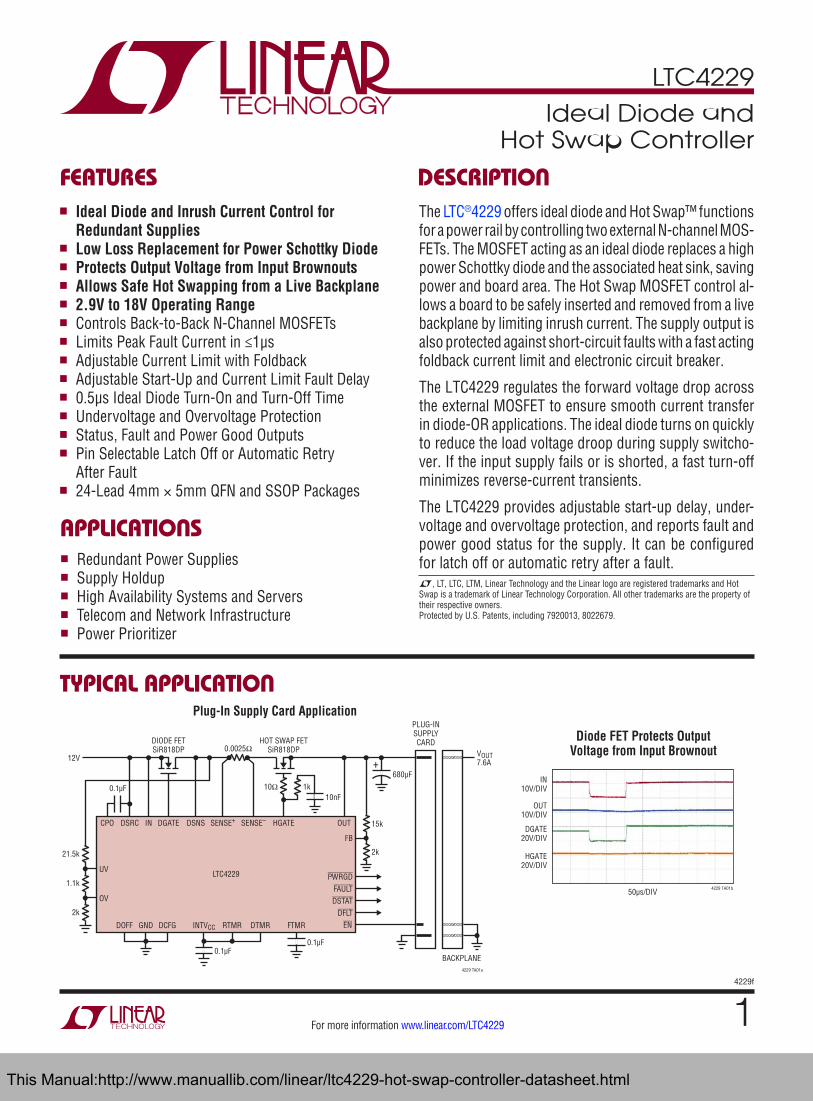
The LTC®4229 offers ideal diode and Hot Swap™ functionsfor a power rail by controlling two external N-channel MOSFETs.The MOSFET acting as an ideal diode replaces a highpower Schottky diode and the associated heat sink, savingpower and board area. The Hot Swap MOSFET control allowsa board to be safely inserted and removed from a livebackplane by limiting inrush current. The supply output isalso protected against short-circuit faults with a fast actingfoldback current limit and electronic circuit breaker.
ManualLib.com collects and classifies the global productinstrunction manuals to help users access anytime andanywhere, helping users make better use of products.
http://www.manuallib.com
LTC4229
14229f
For more information www.linear.com/LTC4229
Typical applicaTion
FeaTures DescripTion
Ideal Diode and Hot Swap Controller
The LTC®4229 offers ideal diode and Hot Swap™ functions for a power rail by controlling two external N-channel MOS-FETs. The MOSFET acting as an ideal diode replaces a high power Schottky diode and the associated heat sink, saving power and board area. The Hot Swap MOSFET control al-lows a board to be safely inserted and removed from a live backplane by limiting inrush current. The supply output is also protected against short-circuit faults with a fast acting foldback current limit and electronic circuit breaker.
The LTC4229 regulates the forward voltage drop across the external MOSFET to ensure smooth current transfer in diode-OR applications. The ideal diode turns on quickly to reduce the load voltage droop during supply switcho-ver. If the input supply fails or is shorted, a fast turn-off minimizes reverse-current transients.
The LTC4229 provides adjustable start-up delay, under-voltage and overvoltage protection, and reports fault and power good status for the supply. It can be configured for latch off or automatic retry after a fault.L, LT, LTC, LTM, Linear Technology and the Linear logo are registered trademarks and Hot Swap is a trademark of Linear Technology Corporation. All other trademarks are the property of their respective owners. Protected by U.S. Patents, including 7920013, 8022679.
Plug-In Supply Card Application
applicaTions
n Ideal Diode and Inrush Current Control for Redundant Supplies
n Low Loss Replacement for Power Schottky Dioden Protects Output Voltage from Input Brownoutsn Allows Safe Hot Swapping from a Live Backplanen 2.9V to 18V Operating Rangen Controls Back-to-Back N-Channel MOSFETsn Limits Peak Fault Current in ≤1µsn Adjustable Current Limit with Foldbackn Adjustable Start-Up and Current Limit Fault Delayn 0.5µs Ideal Diode Turn-On and Turn-Off Timen Undervoltage and Overvoltage Protectionn Status, Fault and Power Good Outputsn Pin Selectable Latch Off or Automatic Retry
After Faultn 24-Lead 4mm × 5mm QFN and SSOP Packages
n Redundant Power Suppliesn Supply Holdupn High Availability Systems and Serversn Telecom and Network Infrastructuren Power Prioritizer
Diode FET Protects Output Voltage from Input Brownout
DCFGDOFF EN
4229 TA01a
DFLT
GND INTVCC
FB
SENSE+ SENSE–
UV
OV DSTAT
RTMR
FAULTPWRGD
DTMR FTMR
CPO DSRC HGATEIN DSNS
BACKPLANE
OUT
10Ω 1k
680µF
10nF
12V VOUT7.6A
HOT SWAP FETSiR818DP
PLUG-INSUPPLYCARD
DGATE
DIODE FETSiR818DP 0.0025Ω
21.5k
1.1k
2k
+
0.1µF
0.1µF0.1µF
15k
2k
LTC4229
50µs/DIV
IN10V/DIV
OUT10V/DIV
DGATE20V/DIV
HGATE20V/DIV
4229 TA01b
This Manual:http://www.manuallib.com/linear/ltc4229-hot-swap-controller-datasheet.html

LTC4229
24229f
For more information www.linear.com/LTC4229
absoluTe MaxiMuM raTingsSupply Voltages
IN ........................................................... –0.3V to 24V INTVCC ..................................................... –0.3V to 7V
Input Voltages FB, DCFG ................................................. –0.3V to 7V FTMR, DTMR, RTMR .............–0.3V to INTVCC + 0.3V UV, OV, EN, DOFF ................................... –0.3V to 24V SENSE+, SENSE–, DSNS, DSRC ............. –0.3V to 24V
Output Voltages FAULT, PWRGD, DSTAT, DFLT, OUT ........ –0.3V to 24V CPO, DGATE (Note 3) ............................. –0.3V to 35V HGATE (Note 4) ..................................... –0.3V to 35V
Average Currents FAULT, PWRGD, DSTAT, DFLT ...............................5mA INTVCC .................................................................1mA
Operating Ambient Temperature Range LTC4229C ................................................ 0°C to 70°C LTC4229I .............................................–40°C to 85°C
Storage Temperature Range .................. –65°C to 150°CLead Temperature (Soldering, 10 sec)
G Package ......................................................... 300°C
(Notes 1, 2)
orDer inForMaTionLEAD FREE FINISH TAPE AND REEL PART MARKING* PACKAGE DESCRIPTION TEMPERATURE RANGE
LTC4229CUFD#PBF LTC4229CUFD#TRPBF 4229 24-Lead (4mm × 5mm) Plastic QFN 0°C to 70°C
LTC4229IUFD#PBF LTC4229IUFD#TRPBF 4229 24-Lead (4mm × 5mm) Plastic QFN –40°C to 85°C
LTC4229CG#PBF LTC4229CG#TRPBF LTC4229G 24-Lead Plastic SSOP 0°C to 70°C
LTC4229IG#PBF LTC4229IG#TRPBF LTC4229G 24-Lead Plastic SSOP –40°C to 85°C
Consult LTC Marketing for parts specified with wider operating temperature ranges. *The temperature grade is identified by a label on the shipping container. Consult LTC Marketing for information on nonstandard lead based finish parts.For more information on lead free part marking, go to: http://www.linear.com/leadfree/ For more information on tape and reel specifications, go to: http://www.linear.com/tapeandreel/
8 9
TOP VIEW
25
UFD PACKAGE24-LEAD (4mm × 5mm) PLASTIC QFN
10 11 12
24 23 22 21 20
6
5
4
3
2
1DSRC
SENSE–
SENSE+
IN
DSNS
INTVCC
GND
PWRGD
FAULT
DSTAT
DFLT
DOFF
DCFG
OV
DGAT
E
CPO
HGAT
E
OUT
FB
DTM
R
RTM
R
FTM
R EN UV
7
14
15
16
17
18
19
13
TJMAX = 125°C, θJA = 43°C/W (Note 5)
EXPOSED PAD (PIN 25) PCB GND CONNECTION OPTIONAL
1
2
3
4
5
6
7
8
9
10
11
12
TOP VIEW
G PACKAGE24-LEAD PLASTIC SSOP
24
23
22
21
20
19
18
17
16
15
14
13
CPO
DGATE
DSRC
SENSE–
SENSE+
IN
DSNS
INTVCC
GND
DTMR
RTMR
FTMR
HGATE
OUT
FB
PWRGD
FAULT
DSTAT
DFLT
DOFF
DCFG
OV
UV
EN
TJMAX = 125°C, θJA = 88°C/W
pin conFiguraTion
This Manual:http://www.manuallib.com/linear/ltc4229-hot-swap-controller-datasheet.html

LTC4229
34229f
For more information www.linear.com/LTC4229
elecTrical characTerisTics The l denotes the specifications which apply over the full operating temperature range, otherwise specifications are at TA = 25°C. VIN = 12V, unless otherwise noted.
SYMBOL PARAMETER CONDITIONS MIN TYP MAX UNITS
Supplies
VIN Input Supply Range l 2.9 18 V
IIN Input Supply Current l 2 4 mA
VINTVCC Internal Regulator Voltage I = 0, –500µA l 4.5 5 5.5 V
VINTVCC(UVL) Internal VCC Undervoltage Lockout INTVCC Rising l 2.1 2.2 2.3 V
∆VINTVCC(HYST) Internal VCC Undervoltage Lockout Hysteresis l 30 60 90 mV
Ideal Diode Control
∆VFWD(REG) Forward Regulation Voltage (VIN – VDSNS) l 35 50 65 mV
∆VDGATE External N-Channel Gate Drive (VDGATE – VDSRC)
IN < 7V, ∆VFWD = 0.15V; I = 0, –1µA IN = 7V to 18V, ∆VFWD = 0.15V; I = 0, –1µA
l
l
5 10
7 12
14 14
V V
∆VDGATE(ST) Diode MOSFET On Detect Threshold (VDGATE – VDSRC)
DSTAT Pulls Low, ∆VFWD = 75mV l 0.3 0.7 1.1 V
∆VFWD(FLT) Open Diode MOSFET Threshold (VIN – VDSNS) DFLT Pulls Low l 200 250 300 mV
IDSNS DSNS Pin Current DSNS = 12V l 50 150 300 µA
IDSRC DSRC Pin Current DSRC = 0V l –95 –150 µA
ICPO(UP) CPO Pull-Up Current CPO = DSRC = IN = 2.9V CPO = DSRC = IN = 18V
l
l
–70 –60
–105 –95
–130 –120
µA µA
IDGATE(FPU) DGATE Fast Pull-Up Current ∆VFWD = 0.2V, ∆VDGATE = 0V, CPO = 17V –1.5 A
IDGATE(FPD) DGATE Fast Pull-Down Current ∆VFWD = –0.2V, ∆VDGATE = 5V 1.5 A
IDGATE(DN) DGATE Off Pull-Down Current DOFF = 2V, ∆VDGATE = 2.5V l 50 100 200 µA
tON(DGATE) DGATE Turn-On Delay ∆VFWD = 0.2V , CDGATE = 10nF l 0.25 0.5 µs
tOFF(DGATE) DGATE Turn-Off Delay ∆VFWD = –0.2V, CDGATE = 10nF l 0.2 0.5 µs
tPLH(DGATE) DOFF Low to DGATE High l 50 100 µs
Hot Swap Control
∆VSENSE(TH) Current Limit Sense Voltage Threshold (VSENSE
+ – VSENSE–)
FB = 1.23V FB = 0V
l
l
22.5 6
25 8.3
27.5 10.6
mV mV
VSENSE+(UVL) SENSE+ Undervoltage Lockout SENSE+ Rising l 1.8 1.9 2 V
∆VSENSE+(HYST) SENSE+ Undervoltage Lockout Hysteresis l 10 50 90 mV
ISENSE+ SENSE+ Pin Current SENSE+ = 11V, IN = 12V, OUT = 0V
SENSE+ = 13V, IN = 12V, OUT = 0Vl
l
150 300 2
450 4
µA mA
ISENSE– SENSE– Pin Current SENSE– = 12V l 10 40 100 µA
∆VHGATE External N-Channel Gate Drive (VHGATE – VOUT)
IN < 7V; I = 0, –1µA IN = 7V to 18V; I = 0, –1µA
l
l
5 10
7 12
14 14
V V
∆VHGATE(H) Gate High Threshold (VHGATE – VOUT) l 3.6 4.2 4.8 V
IHGATE(UP) External N-Channel Gate Pull-Up Current Gate Drive On, HGATE = 0V l –7 –10 –13 µA
IHGATE(DN) External N-Channel Gate Pull-Down Current Gate Drive Off, OUT = 12V, HGATE = OUT + 5V
l 1 2 4 mA
IHGATE(FPD) External N-Channel Gate Fast Pull-Down Current
Fast Turn-Off, OUT = 12V, HGATE = OUT + 5V
l 100 200 350 mA
tPHL(SENSE) Sense Voltage (SENSE+ – SENSE–) High to HGATE Low
∆VSENSE = 200mV, CHGATE = 10nF l 0.5 1 µs
tOFF(HGATE) OV High to HGATE Low UV Low to HGATE Low EN High to HGATE Low SENSE+ Low to HGATE Low
l
l
l
l
10 10 20 10
20 20 40 20
µs µs µs µs
This Manual:http://www.manuallib.com/linear/ltc4229-hot-swap-controller-datasheet.html

LTC4229
44229f
For more information www.linear.com/LTC4229
elecTrical characTerisTics The l denotes the specifications which apply over the full operating temperature range, otherwise specifications are at TA = 25°C. VIN = 12V, unless otherwise noted.
SYMBOL PARAMETER CONDITIONS MIN TYP MAX UNITS
tD(HGATE) UV High, EN Low to HGATE Turn-On Delay DTMR = INTVCC l 50 100 150 ms
tP(HGATE) UV to HGATE Propagation Delay UV = Step 0.8V to 2V l 10 20 µs
Input/Output Pin
VDOFF(H,TH) DOFF Pin High Threshold DOFF Rising l 1.21 1.235 1.26 V
VDOFF(L,TH) DOFF Pin Low Threshold DOFF Falling l 1.19 1.215 1.24 V
∆VDOFF(HYST) DOFF Pin Hysteresis l 10 20 30 mV
VIN(TH) UV, OV, FB Pin Threshold Voltage Voltage Rising l 1.21 1.235 1.26 V
∆VUV(HYST) UV Pin Hysteresis l 40 80 120 mV
∆VOV(HYST) OV Pin Hysteresis l 10 20 30 mV
∆VFB(HYST) FB Pin Hysteresis l 10 20 30 mV
VUV(RESET) UV Pin Fault Reset Threshold Voltage UV Falling l 0.57 0.6 0.63 V
IIN(LEAK) Input Leakage Current (UV, OV, FB, DOFF) V = 5V l 0 ±1 µA
VEN(TH) EN Pin Threshold Voltage EN Rising l 1.185 1.235 1.284 V
∆VEN(HYST) EN Pin Hysteresis l 60 110 160 mV
IEN(UP) EN Pull-Up Current EN = 1V l –7 –10 –13 µA
VTMR(H) FTMR, DTMR, RTMR Pin High Threshold l 1.198 1.235 1.272 V
VTMR(L) FTMR, DTMR, RTMR Pin Low Threshold l 0.15 0.2 0.25 V
IFTMR(UP) FTMR Pull-Up Current FTMR = 1V, In Fault Mode l –80 –100 –120 µA
IFTMR(DN) FTMR Pull-Down Current FTMR = 2V, No Faults l 1.3 2 2.6 µA
IFTMR(RATIO) FTMR Current Ratio IFTMR(DN)/IFTMR(UP) l 1.3 2 2.7 %
ITMR(UP) DTMR, RTMR Pull-Up Current V = 0V l –8 –10 –12 µA
ITMR(DN) DTMR, RTMR Pull-Down Current V = 1.5V l 1 5 10 mA
VIH Input High Voltage (DTMR, RTMR) l INTVCC – 0.1
INTVCC + 0.1
V
VDCFG(TH) Logic Input Threshold (DCFG) l 0.5 2 V
IOUT OUT Pin Current OUT = 11V, IN = 12V, SENSE+ = 11.5V OUT = 13V, IN = 12V, SENSE+ = 11.5V
l
l
40 1.7
100 4
µA mA
VOL Output Low Voltage (PWRGD, FAULT, DSTAT, DFLT)
I = 1mA I = 3mA
l
l
0.15 0.4
0.4 1.2
V V
VOH Output High Voltage (PWRGD, FAULT, DFLT)
I = –1µA l INTVCC – 1
INTVCC – 0.5
V
IOH Input Leakage Current (PWRGD, FAULT, DSTAT, DFLT)
V = 18V l 0 ±1 µA
IPU Output Pull-Up Current (PWRGD, FAULT, DFLT)
V = 1.5V l –7 –10 –13 µA
tRST(UV) UV Low to FAULT High l 20 40 µs
tPG(FB) FB Low to PWRGD High l 20 40 µs
Note 1: Stresses beyond those listed under Absolute Maximum Ratings may cause permanent damage to the device. Exposure to any Absolute Maximum Rating condition for extended periods may affect device reliability and lifetime.Note 2: All currents into device pins are positive; all currents out of device pins are negative. All voltages are referenced to GND unless otherwise specified.
Note 3: An internal clamp limits the DGATE and CPO pins to a minimum of 10V above and a diode below DSRC. Driving these pins to voltages beyond the clamp may damage the device.Note 4: An internal clamp limits the HGATE pin to a minimum of 10V above and a diode below OUT. Driving this pin to voltages beyond the clamp may damage the device.Note 5: Thermal resistance is specified when the exposed pad is soldered to a 3" × 4.5", four layer, FR4 board.
This Manual:http://www.manuallib.com/linear/ltc4229-hot-swap-controller-datasheet.html

LTC4229
54229f
For more information www.linear.com/LTC4229
Typical perForMance characTerisTics
INTVCC Load Regulation Hot Swap Gate Voltage vs CurrentHot Swap Gate Voltage vs IN Voltage
IN Supply Current vs Voltage SENSE+ Current vs Voltage OUT Current vs Voltage
TA = 25°C, VIN = 12V, unless otherwise noted.
CPO Voltage vs Current Diode Gate Voltage vs Current Diode Gate Voltage vs IN Voltage
VIN (V)0
I IN (m
A)
2.0
2.5
3.0
9 15 18
4229 G01
1.5
0.5
1.0
03 6 12
VOUT = 3.3V
VOUT = 0V VOUT = 12V
VSENSE+ = VIN – 0.5V
VOUT (V)0
I OUT
(mA)
1.5
2.0
9 15 18
4229 G03
1.0
0
0.5
–0.53 6 12
VIN = 12V, VSENSE+ = 11.5V
ILOAD (mA)0
INTV
CC (V
)
3
4
5
6
–0.6 –1
4229 G04
2
1
0–0.2 –0.4 –0.8
VIN = 2.9V
VIN = 12V
IHGATE (µA)0
∆ V H
GATE
(V)
8
10
12
14
–6 –12–10
4229 G05
6
4
2
0–2 –4 –8
VIN = 2.9V
VIN = 12V
VOUT = VIN
VIN (V)0
∆ V H
GATE
(V)
8
10
12
14
9 1815
4229 G06
6
43 6 12
VOUT = VIN
ICPO (µA)0
VCP
O –
V DSR
C (V
)
2
4
6
8
10
12
–60 –120–100
4229 G07
0
–2–20 –40 –80
VIN = 2.9V
VIN = 18V
VDRSC = VIN
IDGATE (µA)0
∆VDG
ATE
(V)
2
4
6
8
10
12
–60 –120–100
4229 G08
0
–2–20 –40 –80
VIN = 18V
VIN = 2.9V
VDSNS = VIN – 0.15V
VIN (V)0
∆VDG
ATE
(V)
8
10
12
14
9 1815
4229 G09
6
43 6 12
VDSNS = VIN – 0.15VVDSRC = VIN
VSENSE+ (V)
0
I SEN
SE+ (m
A)
2.0
2.5
3.0
9 15 18
4229 G02
1.5
0.5
1.0
03 6 12
VIN = 12V, VOUT = 0V
This Manual:http://www.manuallib.com/linear/ltc4229-hot-swap-controller-datasheet.html

LTC4229
64229f
For more information www.linear.com/LTC4229
Typical perForMance characTerisTics
Ideal Diode Start-Up Waveform on IN Power-Up
Ideal Diode Turn-On and Turn-Off Waveform
100ms HGATE Start-Up Delay with DTMR Pin Connected to INTVCC
TA = 25°C, VIN = 12V, unless otherwise noted.
Current Limit Threshold FoldbackCurrent Limit Delay vs Sense Voltage
PWRGD, FAULT, DSTAT, DFLT Output Low Voltage vs Current
Adjustable HGATE Start-Up Delay with 0.1µF Capacitor at DTMR Pin
FB VOLTAGE (V)0
CURR
ENT
LIM
IT S
ENSE
VOL
TAGE
V S
ENSE
+ – V
SENS
E– (mV)
10
15
20
25
30
0.6 1.41.21
4229 G10
5
00.2 0.4 0.8
SENSE VOLTAGE (VSENSE+ – VSENSE–) (mV)0
CURR
ENT
LIM
IT D
ELAY
(µs)
10
100
120 200
4229 G11
1
0.140 80 160
CHGATE = 10nF
CURRENT (mA)0
OUTP
UT L
OW V
OLTA
GE (V
)
0.4
1.0
3 5
4229 G12
0.2
0.8
0.6
01 2 4
VIN = 12V
VIN = 2.9V
10ms/DIV
IN10V/DIV
OUT10V/DIV
10V/DIVDSNS
10V/DIV
4229 G13
CPODGATE
1ms/DIV
DOFF5V/DIV
DSTAT10V/DIV
DGATE10V/DIV
DSNS10V/DIV
4229 G14
20ms/DIV
UV5V/DIV
PWRGD10V/DIV
HGATE10V/DIV
OUT10V/DIV
4229 G15 20ms/DIV
UV5V/DIV
PWRGD10V/DIV
HGATE10V/DIV
OUT10V/DIV
4229 G16
This Manual:http://www.manuallib.com/linear/ltc4229-hot-swap-controller-datasheet.html

LTC4229
74229f
For more information www.linear.com/LTC4229
pin FuncTionsCPO: Charge Pump Output. Connect a capacitor from CPO to the DSRC pin. The value of this capacitor is ap-proximately 10× the gate capacitance (CISS) of the external MOSFET for ideal diode control. The charge stored on this capacitor is used to pull up the ideal diode MOSFET gate during a fast turn-on. Leave this pin open if fast ideal diode turn-on is not needed.
DCFG: Logic Input. Configures status indication of DFLT output depending on diode sense (DSNS) connection. Connect this pin to GND when the diode sense is only across the ideal diode MOSFET. Connect to INTVCC when the diode sense is across the ideal diode MOSFET, sense resistor and Hot Swap MOSFET.
DFLT: Diode MOSFET Fault Status Output. This pin is pulled low by an internal switch when the voltage between IN and DSNS exceeds 250mV. The external ideal diode MOSFET is not turned off during the fault. An internal 10µA current source pulls this pin up to a diode below INTVCC. It may be pulled above INTVCC using an external pull-up. Leave open if unused.
DGATE: Ideal Diode MOSFET Gate Drive Output. Connect this pin to the gate of an external N-channel MOSFET for ideal diode control. An internal clamp limits the gate voltage to 12V above and a diode voltage below DSRC. During fast turn-on, a 1.5A pull-up charges DGATE from CPO. During fast turn-off, a 1.5A pull-down discharges DGATE to DSRC.
DOFF: Control Input. A rising edge above 1.235V turns off the external ideal diode MOSFET and a falling edge below 1.215V allows the MOSFET to be turned on.
DSNS: Ideal Diode Output Voltage Sense Input. Connect this pin to the output of either the ideal diode MOSFET or the Hot Swap MOSFET for diode output sense. The voltage sensed at this pin is used to control DGATE for forward voltage regulation and reverse turn-off.
DSRC: Ideal Diode’s MOSFET Gate Drive Return. Connect this pin to the source of the external N-channel MOSFET switch. The gate fast pull-down current returns through this pin when DGATE is discharged.
DSTAT: Diode MOSFET Status Output. Open drain output that pulls low when the MOSFET gate drive voltage between DGATE and DSRC exceeds 0.7V. Otherwise it goes high impedance and requires an external pull-up resistor to a positive supply as there is no internal 10µA current source at this pin. Leave open if unused.
DTMR: Debounce Timer Capacitor Terminal. Connect this pin to either INTVCC for fixed 100ms delay or an external capacitor to ground for adjustable start-up delay (123ms/µF) when EN toggles low.
EN: Enable Input. Ground this pin to enable Hot Swap con-trol. If this pin is pulled high, the MOSFET is not allowed to turn on. A 10µA current source pulls this pin up to a diode below INTVCC. Upon EN going low when UV is high and OV is low, there is a start-up delay for debounce as configured at the DTMR pin, after which the fault is cleared.
Exposed Pad (UFD Package): The exposed pad may be left open or connected to device ground.
FAULT: Overcurrent Fault Status Output. Output that pulls low when the fault filter times out during an overcurrent fault. Otherwise it is pulled high by a 10µA current source to a diode below INTVCC. It may be pulled above INTVCC using an external pull-up. Leave open if unused.
FB: Foldback and Power Good Comparator Input. Connect this pin to an external resistive divider from OUT. If the voltage falls below 1.215V, the PWRGD pin pulls high to indicate the power is bad. If the voltage falls below 0.9V, the output power is considered bad and the current limit is reduced. Tie to INTVCC to disable foldback.
FTMR: Fault Timer Capacitor Terminal. Connect a capacitor between this pin and ground to set a 12ms/µF duration for current limit before the external Hot Swap MOSFET is turned off. The duration of the off time is 11s/µF, resulting in a 0.1% duty cycle.
GND: Device Ground.
This Manual:http://www.manuallib.com/linear/ltc4229-hot-swap-controller-datasheet.html

LTC4229
84229f
For more information www.linear.com/LTC4229
pin FuncTionsHGATE: Hot Swap MOSFET Gate Drive Output. Connect this pin to the gate of the external N-channel MOSFET for Hot Swap control. An internal 10µA current source charges the MOSFET gate. An internal clamp limits the gate voltage to 12V above and a diode voltage below OUT. During an undervoltage or overvoltage generated turn-off, a 2mA pull-down discharges HGATE to ground. During an output short or INTVCC undervoltage lockout, a fast 200mA pull-down discharges HGATE to OUT.
IN: Positive Supply Input. The 5V INTVCC supply is gener-ated from IN, SENSE+ and OUT via an internal diode-OR. The voltage sensed at this pin is used to control DGATE.
INTVCC: Internal 5V Supply Decoupling Output. This pin must have a 0.1µF or larger capacitor. An external load of less than 500µA can be connected at this pin. An undervolt-age lockout threshold of 2.2V will turn off both MOSFETs.
OUT: Hot Swap’s MOSFET Gate Drive Return. Connect this pin to the output side of the external MOSFET. The gate fast pull-down current returns through this pin when HGATE is discharged.
OV: Overvoltage Comparator Input. Connect this pin to an external resistive divider from IN or SENSE+ to monitor the supply overvoltage condition. If the voltage at this pin rises above 1.235V, an overvoltage fault is detected and the Hot Swap MOSFET turns off. Tie to GND if unused.
PWRGD: Power Status Output. Output that pulls low when the FB pin rises above 1.235V and the MOSFET gate drive between HGATE and OUT exceeds 4.2V. Otherwise it is pulled high by a 10µA current source to a diode below INTVCC. It may be pulled above INTVCC using an external pull-up. Leave open if unused.
RTMR: Auto-Retry Timer Capacitor Terminal. Connect this pin to INTVCC for fault latch off. Leave open for auto-retry with 0.1% duty cycle after a fault. Connect an external capacitor to extend the Hot Swap MOSFET off time set by the FTMR pin capacitor to less than 0.1% auto-retry duty cycle after a fault.
SENSE+: Positive Current Sense Input. Connect this pin to the input of the current sense resistor. The voltage sensed at this pin is used for monitoring the current limit. This pin has an undervoltage lockout threshold of 1.9V that will turn off the Hot Swap MOSFET.
SENSE–: Negative Current Sense Input. Connect this pin to the output of the current sense resistor. The current limit circuit controls HGATE to limit the voltage between SENSE+ and SENSE– to 25mV or less depending on the voltage at the FB pin.
UV: Undervoltage Comparator Input. Connect this pin to an external resistive divider from IN or SENSE+ to monitor the supply undervoltage condition. If the voltage at this pin falls below 1.155V, an undervoltage fault is detected and the Hot Swap MOSFET turns off. Pulling the UV pin below 0.6V resets the fault latch after an overcurrent fault. Tie to INTVCC if unused.
This Manual:http://www.manuallib.com/linear/ltc4229-hot-swap-controller-datasheet.html

LTC4229
94229f
For more information www.linear.com/LTC4229
block DiagraM
+–DSRC
DSTATDGATE
0.7V
+ –+–
CL
+ –
+–OUT
PG2HGATE
DCFG
4.2V
+ –
+–1.235V
PG1FB
+–1.235V
DOFFDGATE OFF
LOGIC
5V LDO
DOFF
+–1.235V
OVHGATE OFF
OV
+–1.235V
INTVCC
EN
10µAINTVCC
EN
4229 BD
DFLT
GND
EXPOSED PAD
+–1.9V
UVLO2
GATEDRIVER CHARGE
PUMPf = 2MHz
+–2.2V
UVLO1INTVCC
0.9V
FOLDBACKFB
SENSE+
SENSE–
–+
–+
0.6V
RSTFAULT RESET
1.235V
UV
UV
TM5
TM6
HGATE ON–+
––+
INTVCC
10µA
DSTAT
INTVCC
10µA
100µA10µA
0.2V
1.235VRTMR
FAULT
INTVCC
10µA
PWRGD
0.1V
+–
10µA
INTVCC
TM3
TM4–+
––+
0.2V
+–
1.235VDTMR
0.1V
+–
10µA
INTVCC
TM1
DFLT
TM2–+
–+
0.2V
1.235V
FTMR
DGATE
CPO
DSRC
50mV
GD
100µA
2µA
HGATE
12V
IN DSNSOUT
+–+
–250mV
+ –
12V
This Manual:http://www.manuallib.com/linear/ltc4229-hot-swap-controller-datasheet.html

LTC4229
104229f
For more information www.linear.com/LTC4229
operaTionThe LTC4229 functions as an ideal diode with inrush cur-rent limiting and overcurrent protection. It controls two external N-channel MOSFETs on a supply path, a diode MOSFET (MD) and a Hot Swap MOSFET (MH).
When the LTC4229 is first powered up, the gates of the external MOSFETs are held low, keeping them off. The gate drive amplifier (GD) monitors the voltage between the IN and DSNS pins and drives the DGATE pin. The amplifier quickly pulls up the DGATE pin, turning on the MOSFET for ideal diode control, when it senses a large forward voltage drop. An external capacitor connected between the CPO and DSRC pins provides the charge needed to quickly turn on the ideal diode MOSFET. An internal charge pump charges up this capacitor at device power-up. The DGATE pin sources current from the CPO pin and sinks current into the DSRC and GND pins. When the DGATE to DSRC voltage exceeds 0.7V, the DSTAT pin pulls low to indicate that the ideal diode MOSFET is turned on.
If the LTC4229 is out of undervoltage and overvoltage conditions, pulling the EN pin low initiates a debounce timing cycle that can be a fixed 100ms or adjustable delay as configured at the DTMR pin. After this timing cycle, a 10µA current source from the charge pump ramps up the HGATE pin. When the Hot Swap MOSFET turns on, the inrush current is limited at a level set by an external sense resistor (RS) connected between the SENSE+ and SENSE– pins. An active current limit amplifier (CL) servos the gate of the MOSFET to 25mV or less across the cur-rent sense resistor depending on the voltage at the FB pin. Inrush current can be further reduced, if desired, by adding a capacitor from HGATE to GND. When FB voltage rises above 1.235V and the MOSFET’s gate drive (HGATE to OUT voltage) exceeds 4.2V, the PWRGD pin pulls low.
When both of the MOSFETs are turned on, the gate drive amplifier controls DGATE to servo the forward voltage drop (VIN – VDSNS) across the sense resistor and the two
MOSFETs to 50mV if DSNS and OUT pins are connected together. If the load current causes more than 50mV of voltage drop, the DGATE voltage rises to enhance the MOSFET used for ideal diode control. For large output currents, the ideal diode MOSFET is driven fully on and the voltage drop across the MOSFETs is equal to the sum of the ILOAD • RDS(ON) of the two MOSFETs in series. However, if DSNS and SENSE+ pins are connected together, the gate drive amplifier attempts to regulate 50mV across the ideal diode MOSFET only regardless of the ILOAD • RDS(ON) drop across the Hot Swap MOSFET.
In the case of an input supply short circuit when the MOS-FETs are conducting, a large reverse current starts flowing from the load towards the input. The gate drive amplifier detects this failure condition and turns off the ideal diode MOSFET by pulling down the DGATE pin.
In the case where an overcurrent fault occurs on the supply output, the current is limited with foldback. After a delay set by 100µA charging the FTMR pin capacitor, the fault filter times out and pulls the HGATE pin low, turning off the Hot Swap MOSFET. The FAULT pin is also latched low. At this point, the DGATE pin continues to pull high and keeps the ideal diode MOSFET on.
Internal clamps limit both the DGATE to DSRC and CPO to DSRC voltages to 12V. The same clamps also limit the CPO and DGATE pins to a diode voltage below the DSRC pin. Another internal clamp limits the HGATE to OUT voltage to 12V and also clamps the HGATE pin to a diode voltage below the OUT pin.
Power to the LTC4229 is supplied from either the IN, SENSE+ or OUT pins, through an internal diode-OR circuit to a low dropout regulator (LDO). That LDO generates a 5V supply at the INTVCC pin and powers the LTC4229’s internal low voltage circuitry
This Manual:http://www.manuallib.com/linear/ltc4229-hot-swap-controller-datasheet.html

LTC4229
114229f
For more information www.linear.com/LTC4229
High availability systems often employ parallel-connected power supplies or battery feeds to achieve redundancy and enhance system reliability. Power ORing diodes are commonly used to connect these supplies at the point of load at the expense of power loss due to significant diode forward voltage drop. The LTC4229 minimizes this power loss by using an external N-channel MOSFET as the pass element, allowing for a low voltage drop from the supply to the load when the MOSFET is turned on. When an input source voltage drops below the output common supply voltage, the appropriate MOSFET is turned off, thereby matching the function and performance of an ideal diode. By adding a current sense resistor in between the two external MOSFETs that are separately controlled, the LTC4229 enhances the ideal diode performance with inrush current limiting and overcurrent protection (see Figure 1). This allows the board to be safely inserted and removed from a live backplane without damaging the connector.
applicaTions inForMaTionInternal VCC Supply
The LTC4229 operates with an input supply from 2.9V to 18V. The power supply to the device is internally regulated at 5V by a low dropout regulator (LDO) with an output at the INTVCC pin. An internal diode-OR circuit selects the highest of the supplies at the IN, SENSE+ and OUT pins to power the device through the LDO. The diode-OR scheme permits the device’s power to be kept alive by the OUT voltage when the IN and SENSE+ supplies have collapsed or shut off.
An undervoltage lockout circuit prevents all of the MOSFETs from turning on until the INTVCC voltage exceeds 2.2V. A 0.1µF capacitor is recommended between the INTVCC and GND pins, close to the device for bypassing. No external supply should be connected at the INTVCC pin so as not to affect the LDO’s operation. A small external load of less than 500µA can be connected at the INTVCC pin.
Figure 1. Plug-In Card Supplying 12V Power to Backplane
R6100k
R7100k R8
100k
R9100k
DCFGDOFF EN
4229 F01
DFLT
GND INTVCC
FB
SENSE+ SENSE–
UV
OV DSTAT
RTMR
FAULTPWRGD
DTMR FTMR
CPO DSRC HGATEIN DSNS
BACKPLANE
OUT
RH10Ω
RHG1k
CL680µF
CHG10nF
VIN12V
VOUT7.6A
BULK SUPPLYBYPASS
CAPACITOR
MHSiR818DP
PLUG-INSUPPLYCARD
VSENSE+DGATE
MDSiR818DP
RS0.0025Ω
R321.5k
R21.1k
R12k
++
C20.1µF
CFT0.1µF
R515k
R42k
LTC4229
C10.1µF
This Manual:http://www.manuallib.com/linear/ltc4229-hot-swap-controller-datasheet.html

LTC4229
124229f
For more information www.linear.com/LTC4229
applicaTions inForMaTion
Figure 2. DSNS and DCFG Configurations
DSNS and DCFG Configuration
The LTC4229 features the DSNS and DCFG pins that allow a diode-OR circuit output to be configured either at the SENSE+ or OUT pin (see Figure 2). If DSNS is connected to SENSE+, the forward voltage is sensed across the ideal diode MOSFET MD. As the Hot Swap MOSFET MH is not part of the diode sensing, connect the DCFG pin to GND so that the Hot Swap MOSFET gate overdrive will not be considered as a criterion for the ideal diode MOSFET fault status indication at the DFLT pin. If DSNS is connected to OUT, the forward voltage is sensed across the ideal diode MOSFET, sense resistor and Hot Swap MOSFET. Since the Hot Swap MOSFET is part of the diode sensing and is turned off at start-up, the DFLT pin may be falsely pulled low to indicate an open ideal diode MOSFET fault when the forward voltage exceeds 250mV. For such a configuration, connect DCFG pin to INTVCC so that the Hot Swap MOSFET gate overdrive condition will be considered to avoid false indication of the DFLT output status.
Turn-On Sequence
The board power supply at the OUT pin is controlled with two external N-channel MOSFETs (MD, MH) in Figure 1. The MOSFET MD on the supply side functions as an ideal diode, while MH on the load side acts as a Hot Swap controlling the power supplied to the output load. The sense resistor RS monitors the load current for overcurrent detection. The HGATE capacitor CHG controls the gate slew rate to limit the inrush current. Resistor RHG with CHG compensates the current control loop, while RH prevents high frequency oscillations in the Hot Swap MOSFET.
During a normal power-up, the ideal diode MOSFET turns on first. As soon as the internally generated supply, INTVCC, rises above its 2.2V undervoltage lockout threshold, the internal charge pump is allowed to charge up the CPO pin. The gate drive amplifier controls the gate of the ideal diode MOSFET, to servo its forward voltage drop between the IN and DSNS pins to 50mV. If the forward drop is large, the gate drive amplifier will cause DGATE to be pulled up to the CPO pin voltage and drive the MOSFET gate fully on.
Before the Hot Swap MOSFET can be turned on, the UV and OV pin voltage requirements should be met and EN must remain low for a debounce cycle as configured at the DTMR pin, to ensure that any contact bounces during the insertion have ceased. At the end of the debounce cycle, the internal fault latch is cleared. The Hot Swap MOSFET is then allowed to turn on by charging up HGATE with a 10µA current source from the charge pump. The voltage at the HGATE pin rises with a slope equal to 10µA/CHG and the supply inrush current flowing into the load capacitor CL is limited to:
IINRUSH =
CLCHG
•10µA
The OUT voltage follows the HGATE voltage when the Hot Swap MOSFET turns on. If the voltage across the current sense resistor RS becomes too high based on the FB pin voltage, the inrush current will be limited by the internal current limiting circuitry. Once the MOSFET gate overdrive exceeds 4.2V and the FB pin voltage is above 1.235V, the PWRGD pin pulls low to indicate that the power is good.
DCFG
LTC4229*
*ADDITIONAL DETAILS OMITTED FOR CLARITY
4229 F02
DFLT
GND
SENSE+ SENSE–
INTVCC
HGATEIN DSNS
VIN2
OUT
VIN1 VOUT
MH
DGATE
MD RS
D1
C1
DCFG
LTC4229* DFLT
GND
SENSE+ SENSE–
INTVCC
HGATEIN DSNS
VIN2
OUT
VIN1 VOUT
MH
DGATE
MD RS
D1
C1
This Manual:http://www.manuallib.com/linear/ltc4229-hot-swap-controller-datasheet.html

LTC4229
134229f
For more information www.linear.com/LTC4229
applicaTions inForMaTionOnce OUT reaches the input supply voltage, HGATE con-tinues to ramp up. An internal 12V clamp limits the HGATE voltage above OUT.
Turn-Off Sequence
The external MOSFETs can be turned off by a variety of conditions. A normal turn-off for the Hot Swap MOSFET is initiated by pulling the UV pin below its 1.155V threshold (80mV UV pin hysteresis), or pulling the EN pin above its 1.235V threshold. Additionally, an overvoltage fault or overcurrent fault that exceeds the fault filter time-out also turns off the Hot Swap MOSFET. Normally, the LTC4229 turns off the MOSFET by pulling the HGATE pin to ground with a 2mA current sink.
All of the MOSFETs turn off when INTVCC falls below its undervoltage lockout threshold (2.2V). The DGATE pin is pulled down with a 100µA current to one diode voltage below the DSRC pin, while the HGATE pin is pulled down to the OUT pin by a 200mA current.
The gate drive amplifier controls the ideal diode MOSFET to prevent reverse current when the input supply falls below DSNS (connects to either SENSE+ or OUT). If the input supply collapses quickly, the gate drive amplifier turns off the ideal diode MOSFET with a fast pull-down circuit. If the input supply falls at a more modest rate, the gate drive amplifier controls the MOSFET to maintain DSNS at 50mV below IN.
Board Presence Detect with EN
After the input has settled to within the OV and UV limits, and the EN pin goes low indicating a board presence, the LTC4229 initiates a timing cycle as configured at the DTMR pin for contact debounce. It defaults to internal 100ms delay if DTMR is tied to INTVCC. If an external capacitor CDT is connected from the DTMR pin to GND, the delay is given by charging the capacitor to 1.235V with a 10µA current. Thereafter, the capacitor is discharged to ground by a 5mA current. For a given debounce delay, the equation for setting the external capacitor CDT value is:
CDT = tDB • 0.0081 [µF/ms]
Upon board insertion, any bounces on the EN pin restart the timing cycle. When the debounce timing cycle is done, the internal fault latch is cleared. If the EN pin remains low at the end of the timing cycle, HGATE is charged up with a 10µA current source to turn on the Hot Swap MOSFET.
If the EN pin goes high, indicating a board removal, the HGATE pin is pulled low with a 2mA current sink after a 20µs delay, turning off the Hot Swap MOSFET without clearing any latched fault.
Overcurrent Fault
The LTC4229 features an adjustable current limit with foldback that protects the external MOSFET against short circuits or excessive load current. The voltage across the external sense resistor RS is monitored by an active current limit amplifier. The amplifier controls the gate of the Hot Swap MOSFET to reduce the load current as a function of the output voltage sensed by the FB pin during active current limit. A graph in the Typical Performance Characteristics shows the current limit sense voltage versus FB voltage.
An overcurrent fault occurs when the output has been in current limit for longer than the fault filter delay configured at the FTMR pin. Current limiting begins when the sense voltage between the SENSE+ and SENSE– pins reaches 8.3mV to 25mV depending on the FB pin voltage. The gate of the Hot Swap MOSFET is brought under control by the current limit amplifier and the output current is regulated to limit the sense voltage to less than 25mV. At this point, the fault filter starts the timeout with a 100µA current charging the FTMR pin capacitor. If the FTMR pin voltage exceeds its 1.235V threshold, the external MOSFET turns off with HGATE pulled to ground by 2mA, and FAULT pulls low.
After the Hot Swap MOSFET turns off, the FTMR pin ca-pacitor is discharged with a 2µA pull-down current until its threshold reaches 0.2V. This is followed by a cool-off period of 14 timing cycles as described in the FTMR Pin Functions. Figure 3 shows an overcurrent fault on the 12V output.
This Manual:http://www.manuallib.com/linear/ltc4229-hot-swap-controller-datasheet.html

LTC4229
144229f
For more information www.linear.com/LTC4229
applicaTions inForMaTion
In the event of a severe short-circuit fault on the 12V output as shown in Figure 4, the output current can surge to tens of amperes. The LTC4229 responds within 1µs to bring the current under control by pulling the HGATE to OUT voltage down to zero volts. Almost immediately, the gate of the Hot Swap MOSFET recovers rapidly due to the charge stored in the RHG and CHG network, and current is actively limited until the fault filter times out. Due to parasitic supply lead inductance, an input supply without any bypass capacitor may collapse during the high cur-rent surge and then spike upwards when the current is interrupted. Figure 13 shows the input supply transient suppressors consisting of Z1, RSNUB and CSNUB for the supply if there is no input capacitance.
FTMR Pin Functions
An external capacitor CFT connected from the FTMR pin to GND serves as fault filtering when the supply output is in active current limit. When the voltage across the sense
Figure 3. Overcurrent Fault on 12V Output
Figure 4. Severe Short-Circuit on 12V Output
resistor exceeds the foldback current limit threshold (from 25mV to 8.3mV), FTMR pulls up with 100µA. Otherwise, it pulls down with 2µA. The fault filter times out when the 1.235V FTMR threshold is exceeded, causing the FAULT pin to pull low. For a given fault filter delay, the equation for setting the external capacitor CFT value is:
CFT = tFF • 0.083 [µF/ms]
After the fault filter timeout, the FTMR pin capacitor pulls down with 2µA from the 1.235V FTMR threshold until it reaches 0.2V. Then, it completes 14 cooling cycles consist-ing of the FTMR pin capacitor charging to 1.235V with a 100µA current and discharging to 0.2V with a 2µA current. At that point, the HGATE pin voltage is allowed to start up if the fault has been cleared as described in the Resetting Fault section. When the latched fault is cleared during the cool-off period, the FAULT pin pulls high. The total cool-off time for the MOSFET after an overcurrent fault is:
tCOOL = CFT • 11 [s/µF]
After the cool-off period, the HGATE pin is only allowed to pull up if the fault has been cleared for the latchoff configuration. For the auto-retry configuration, the latched fault is cleared automatically following the extended cool-off period and the HGATE pin voltage is allowed to restart.
Resetting Fault
For the latchoff configuration with the RTMR pin tied to INTVCC, an overcurrent fault is latched after fault filter times out, and the FAULT pin is asserted low. To reset a latched fault and restart the output, pull the UV pin below 0.6V for more than 100µs and then high above 1.235V. The fault latch resets and the FAULT pin deasserts on the falling edge of the UV pin. When UV goes high again, a debounce timing cycle is initiated before the HGATE pin voltage restarts. Toggling the EN pin high and then low again also resets a fault, but the FAULT pin pulls high at the end of the debounce cycle before the HGATE pin voltage starts up. Bringing the supply below the INTVCC undervoltage lockout threshold (2.2V) shuts off all the MOSFETs and resets the fault latch. A debounce cycle is initiated before a normal start-up when the supply is restored above the INTVCC UVLO threshold.
200µs/DIV
OUT10V/DIV
HGATE10V/DIV
ILOAD20A/DIV
4229 F03
5µs/DIV
OUT10V/DIV
HGATE10V/DIV
ILOAD20A/DIV
4229 F04
This Manual:http://www.manuallib.com/linear/ltc4229-hot-swap-controller-datasheet.html

LTC4229
154229f
For more information www.linear.com/LTC4229
applicaTions inForMaTionAuto-Retry After a Fault
For the auto-retry configuration, if the RTMR pin is left open, the latched fault is reset automatically at the end of the cool-off period as described in the FTMR Pin Functions section. In this case, the auto-retry duty cycle is equal to 0.1%, irrespective of CFT. If an external capacitor CRT is connected from the RTMR pin to GND, the cool-off time can be further extended by another 15 cooling cycles consist-ing of the RTMR pin capacitor charging to 1.235V with a 10µA current and discharging to 0.2V with a 5mA current. For a given additional cool-off time for the MOSFET, the equation for setting the external capacitor CRT value is:
CRT = tXCOOL • 0.54 [µF/s]
At the end of the extended cool-off period, the fault latch is cleared and FAULT pulls high. The HGATE pin voltage is allowed to start up and turn on the Hot Swap MOSFET. If the output short persists, the supply powers up into a short with active current limiting until the fault filter times out and FAULT again pulls low. A new extended cool-off cycle begins with FTMR ramping down with a 2µA current. The whole process repeats itself until the output short is removed.
The auto-retry duty cycle is given by:
Duty Cycle = tFF
tCOOL + tXCOOL• 100%
For example, if CFT = 0.1µF, CRT = 1µF and tFF = 1.2ms, the auto-retry duty cycle is calculated as 0.04%. Figure 5 shows an auto-retry sequence after an overcurrent fault.
Monitor Overvoltage and Undervoltage Faults
Both the OV and UV pins function as an input supply monitor while UV pin also functions as a turn-on control. A resistive divider connected between the input supply (IN or SENSE+) and GND at the OV and UV pins monitors the supply for overvoltage and undervoltage conditions. The overvoltage and undervoltage thresholds are set by proper selection of the resistors at their respective OV and UV rising threshold voltage (1.235V).
For Figure 1, if R1 = 2k, R2 = 1.1k and R3 = 21.5k, the input supply overvoltage and undervoltage thresholds are set to 15.2V and 9.8V respectively.
An overvoltage fault occurs if the input supply rises above its overvoltage threshold. The Hot Swap MOSFET is turned off by a 2mA pull-down from HGATE to ground. If the input supply subsequently falls below its overvoltage threshold, the Hot Swap MOSFET is allowed to turn on immediately. The OV pin voltage is 1.215V when falling out of overvoltage.
An undervoltage fault occurs if the input supply falls below its undervoltage threshold. If the UV pin voltage falls below 1.155V but remains above 0.6V, the Hot Swap MOSFET is turned off by a 2mA pull-down from HGATE to ground. The Hot Swap MOSFET turns back on instantly without the debounce cycle when the input supply rises above its undervoltage threshold. However, if the UV pin voltage drops below 0.6V, it turns off the Hot Swap MOSFET and clears the fault latch. The Hot Swap MOSFET turns back on only after a debounce cycle when the input supply is restored above its undervoltage threshold.
During the overvoltage and undervoltage fault conditions, FAULT will not be pulled low but PWRGD will be pulled high as HGATE is pulled low. The ideal diode function controlled by the ideal diode MOSFET is not affected by the OV and UV fault conditions.
Power Good Monitor
Internal circuitry monitors the MOSFET gate overdrive between the HGATE and OUT pins. Also, the FB pin that connects to OUT through a resistive divider is used to determine a power good condition. The power good Figure 5. Auto-Retry Sequence After a Fault
500ms/DIV
RTMR2V/DIV
FTMR2V/DIV
FAULT10V/DIV
OUT10V/DIV
4229 F05
This Manual:http://www.manuallib.com/linear/ltc4229-hot-swap-controller-datasheet.html

LTC4229
164229f
For more information www.linear.com/LTC4229
applicaTions inForMaTioncomparator drives high when the FB pin rises above 1.235V, and drives low when FB falls below 1.215V. The power good status for the input supply is reported via an open-drain output, PWRGD. It is normally pulled high by an external pull-up resistor or the internal 10µA pull-up.
The PWRGD pin pulls low when the FB power good com-parator is high and the HGATE drive exceeds 4.2V. The PWRGD pin goes high when the HGATE is turned off by the UV, OV or EN pins, or when the FB power good comparator drives low, or when INTVCC enters undervoltage lockout.
CPO and DGATE Start-Up
In applications where a single ideal diode MOSFET is placed on the supply side, CPO is initially pulled up to a diode below the DSRC pin when first powered up (see Figure 13). In back-to-back MOSFETs applications, CPO starts off at 0V, since DSRC is near ground (see Figure 14). CPO starts ramping up 7µs after INTVCC clears its undervolt-age lockout level. Another 40µs later, DGATE also starts ramping up with CPO. The CPO ramp rate is determined by the CPO pull-up current into the combined CPO and DGATE pin capacitances. An internal clamp limits the CPO pin voltage to 12V above the DSRC pin, while the final DGATE pin voltage is determined by the gate drive amplifier. An internal 12V clamp limits the DGATE pin voltage above DSRC.
CPO Capacitor Selection
The recommended value of the capacitor between the CPO and DSRC pins is approximately 10× the input capacitance CISS of the ideal diode MOSFET. A larger capacitor takes a correspondingly longer time to charge up by the internal charge pump. A smaller capacitor suffers more voltage drop during a fast gate turn-on event as it shares charge with the MOSFET gate capacitance.
MOSFET Selection
The LTC4229 drives N-channel MOSFETs to conduct the load current. The important features of the MOSFETs are on-resistance RDS(ON), the maximum drain-source voltage BVDSS and the threshold voltage.
The gate drive for the ideal diode and Hot Swap MOSFET is guaranteed to be greater than 5V when the supply voltage
at IN is between 2.9V and 7V. When the supply voltage at IN is greater than 7V, the gate drive is guaranteed to be greater than 10V. The gate drive is limited to 14V. An external Zener diode can be used to clamp the potential from the MOSFET’s gate to source if the rated breakdown voltage is less than 14V.
The maximum allowable drain-source voltage BVDSS must be higher than the supply voltage including supply transients as the full supply voltage can appear across the MOSFET. If an input or output is connected to ground, the full supply voltage will appear across the MOSFET. The RDS(ON) should be small enough to conduct the maximum load current, and also stay within the MOSFET’s power rating.
Supply Transient Protection
When the capacitances at the input and output are very small, rapid changes in current during input or output short-circuit events can cause transients that exceed the 24V absolute maximum ratings of the IN and OUT pins. To minimize such spikes, use wider traces or heavier trace plating to reduce the power trace inductance. Also, bypass locally with a 10µF electrolytic and 0.1µF ceramic, or alternatively clamp the input with a transient voltage suppressor Z1. A 100Ω, 0.1µF snubber damps the response and eliminates ringing (see Figure 13).
Design Example
As a design example for selecting components, consider a 12V system with a 7.6A maximum load current for the input supply (see Figure 1).
First, select the appropriate value of the current sense resistor RS for the 12V supply. Calculate the sense resistor value based on the maximum load current ILOAD(MAX) and the lower limit for the current limit sense voltage threshold ∆VSENSE(TH)(MIN).
RS =
ΔVSENSE(TH)(MIN)
ILOAD(MAX)=
22.5mV7.6A
= 2.9mΩ
Choose a 2.5mΩ sense resistor with a 1% tolerance.
Next, calculate the RDS(ON) of the ideal diode MOSFET to achieve the desired forward drop at maximum load.
This Manual:http://www.manuallib.com/linear/ltc4229-hot-swap-controller-datasheet.html

LTC4229
174229f
For more information www.linear.com/LTC4229
applicaTions inForMaTionAssuming a forward drop, ∆VFWD of 50mV across the ideal diode MOSFET:
RDS(ON) ≤
ΔVFWDILOAD(MAX)
=50mV7.6A
= 6.5mΩ
The SiR818DP offers a good choice with a maximum RDS(ON) of 2.8mΩ at VGS = 10V. The input capacitance CISS of the SiR818DP is about 3660pF. Slightly exceeding the 10× recommendation, a 0.1µF capacitor is selected for C2 at the CPO pin.
Next, verify that the thermal ratings of the selected Hot Swap MOSFET are not exceeded during power-up or an overcurrent fault.
Assuming the MOSFET dissipates power due to inrush current charging the load capacitor CL at power-up, the energy dissipated in the MOSFET is the same as the energy stored in the load capacitor, and is given by:
ECL =
12
• CL • VIN2
For CL = 680µF, the time it takes to charge up CL is cal-culated as:
tCHARGE =
CL • VINIINRUSH
=680µF • 12V
1A= 8ms
The inrush current is set to 1A by adding capacitance CHG at the gate of the Hot Swap MOSFET.
CHG =
CL • IHGATE(UP)
IINRUSH=
680µF • 10µA1A
= 6.8nF
Choose a practical value of 10nF for CHG.
The average power dissipated in the MOSFET is calculated as:
PAVG =
ECLtCHARGE
=12
•680µF • 12V( )2
8ms= 6W
The MOSFET selected must be able to tolerate 6W for 8ms during power-up. The SOA curves of the SiR818DP provide 45W (1.5A at 30V) for 100ms. This is sufficient to satisfy the requirement. The increase in junction temperature due to the power dissipated in the MOSFET is ∆T = PAVG • ZthJC where ZthJC is the junction-to-case thermal impedance.
Under this condition, the SiR818DP data sheet indicates that the junction temperature will increase by 3°C using ZthJC = 0.5°C/W (single pulse).
Next, the power dissipated in the MOSFET during an overcurrent fault must be safely limited. The fault timer capacitor (CFT) is used to prevent power dissipation in the MOSFET from exceeding the SOA rating during active current limit. A good way to determine a suitable value for CFT is to superimpose the foldback current limit profile shown in the Typical Performance Characteristics on the MOSFET data sheet’s SOA curves.
For the SiR818DP MOSFET, this exercise yields the plot in Figure 6.
VDS – DRAIN-TO-SOURCE VOLTAGE (V)
I D –
DRA
IN C
URRE
NT (A
)
4229 F06
100
10
1
0.1
0.010.01 10 10010.1
1ms
10ms
100ms
1s
10s
DCBVDSS LIMITED
* VGS > MINIMUM VGSAT WHICH RDS(ON) IS SPECIFIED
ID LIMITED
IDM LIMITED
LIMITED BY RDS(ON)*
MOSFET POWER DISSIPATION CURVE RESULTING FROM FOLDBACK ACTIVE CURRENT LIMIT
Figure 6. SiR818DP SOA with Design Example MOSFET Power Dissipation Superimposed
As can be seen, the LTC4229’s foldback current limit profile roughly coincides with the 100ms SOA contour. Since this SOA plot is for an ambient temperature of 25°C only, a maximum fault filter time of much less than 100ms should be considered, such as 10ms or less. Selecting a 0.1μF ± 10% value for CFT yields a maximum fault filter time of 1.75ms which should be small enough to protect the MOSFET during any overcurrent fault scenario.
Next, select the values for the resistive divider at the OV and UV pins that define the overvoltage and undervoltage threshold of 15.2V and 9.8V respectively for the 12V input supply. Since the leakage currents for the OV and UV pins can be as high as ±1μA each, the total resistance in the divider should be low enough to minimize the resulting
This Manual:http://www.manuallib.com/linear/ltc4229-hot-swap-controller-datasheet.html

LTC4229
184229f
For more information www.linear.com/LTC4229
applicaTions inForMaTionoffset errors. Calculate the bottom resistor R1 based on the following equation to obtain less than ±0.5% error due to leakage current.
R1=
VOV(TH)
2 • IIN(LEAK)
⎛
⎝⎜⎜
⎞
⎠⎟⎟ • 0.5% =
1.235V2µA
⎛
⎝⎜
⎞
⎠⎟ • 0.5% = 3k
Choose R1 to be 2k to achieve less than ±0.5% error and calculating R2/R3 yields:
R2 =VIN(OV)
VIN(UV)– 1
⎛
⎝⎜⎜
⎞
⎠⎟⎟ •R1=
15.2V9.8V
−1⎛
⎝⎜
⎞
⎠⎟ • 2k = 1.1k
R3 =VIN(UV)
VUV(TH)– 1
⎛
⎝⎜⎜
⎞
⎠⎟⎟ • (R1+R2)
R3 =9.8V
1.235V– 1
⎛
⎝⎜
⎞
⎠⎟ • (2k +1.1k) = 21.5k
The worst case OV and UV threshold offset voltage errors resulting from the total UV and OV pin leakage current (2 • IIN(LEAK)) that flows into R3, are calculated as ±0.29% and ±0.44% respectively.
It remains to select the values for the FB pin resistive divider in order to set a power good threshold of 10.5V. Keeping in mind the FB pin’s ±1μA leakage current, choose
a value of 2k for the bottom resistor R4. Calculating the top resistor R5 value yields:
R5 =
VOUT(PG)
VFB(TH)−1
⎛
⎝⎜⎜
⎞
⎠⎟⎟ •R4 =
10.5V1.235V
−1⎛
⎝⎜
⎞
⎠⎟ • 2k = 15k
The subsequent offset error due to the FB pin leakage current will be less than ±0.14%.
The final component to consider is a 0.1µF bypass (C1) at the INTVCC pin.
PCB Layout Considerations
To achieve accurate current sensing, a Kelvin connection for the sense resistor is recommended. The PCB layout should be balanced and symmetrical to minimize wiring errors. In addition, the PCB layout for the sense resistor and the power MOSFET should include good thermal management techniques for optimal device power dissipa-tion. A recommended PCB layout is illustrated in Figure 7.
Connect the IN and OUT pin traces as close as possible to the MOSFET’s terminals. Keep the traces to the MOSFETs wide and short to minimize resistive losses. The PCB traces associated with the power path through the MOSFETs should have low resistance. The suggested trace width for
Figure 7. Recommended PCB Layout for Power MOSFETs and Sense Resistor
C1
MHPowerPAK SO-8
D
D
D
D
S
S
S
G
OUT
CURRENT FLOWTO LOAD
TRACK WIDTH W:0.03" PER AMPEREON 1oz Cu FOIL
VIA TO GND PLANE
W
MDPowerPAK SO-8
G
S
S
S
D
D
D
D
IN
CURRENT FLOWTO LOAD
W
RH
C2
Z1
8 9 10 11 12
24 23 22
LTC4229UFD
21 20
6
5
4
3
2
1
7
14
15
16
17
18
19
13
RS
4229 F07
This Manual:http://www.manuallib.com/linear/ltc4229-hot-swap-controller-datasheet.html

LTC4229
194229f
For more information www.linear.com/LTC4229
applicaTions inForMaTion1oz copper foil is 0.03" for each ampere of DC current to keep PCB trace resistance, voltage drop and temperature rise to a minimum. Note that the sheet resistance of 1oz copper foil is approximately 0.5mΩ/square, and voltage drops due to trace resistance add up quickly in high cur-rent applications.
It is also important to place the bypass capacitor C1 for the INTVCC pin, as close as possible between INTVCC and GND. Also place C2 near the CPO and DSRC pins. The transient voltage suppressor Z1, when used, should be mounted close to the LTC4229 using short lead lengths.
Flexible Configuration for Ideal Diode and Hot Swap MOSFET
The LTC4229 offers the flexibility to swap the ordering of the MD and MH N-channel MOSFETs for the ideal diode and Hot Swap control respectively between the supply and load side.
Figure 8 shows a configuration that allows two input sup-plies to be diode-ORed at SENSE+ pin followed by Hot Swap control for a card-resident application. For applications where the LTC4229 resides on the backplane, the two supplies are diode-ORed at the output as shown in Figures 9 and 10. Figure 11 depicts an application where placing the MD MOSFET downstream of the MH MOSFET allows a dedicated bypass capacitor to keep alive its small load after power is removed at the input. Unlike the circuit in Figure 9 where the SENSE+ pin is protected from momentary negative input transients by the ideal diode, the loads in Figures 10 and 11 are much more susceptible to brownouts. This is because input transients that dip below the SENSE+ pin’s 1.9V UVLO threshold can cause the HGATE pin to pull low thus discharging the MH MOSFET’s gate capacitance as well as any external capacitance which can result in a lengthy recovery time for the Hot Swap controller.
Since the LTC4229’s ideal diode and Hot Swap controllers operate independently, the MD and MH MOSFETs can also be configured to operate on two different supplies at the same time as shown in Figure 12. If one of the supplies is not available, the LTC4229 will continue to operate with the remaining supply since the internal INTVCC regulator is powered from an internal diode-OR of the IN, SENSE+
and OUT pins.
Power Prioritizer
Figure 14 shows an application where either of two sup-plies is passed to the output on the basis of priority, rather than simply allowing the highest voltage to prevail. The 5V primary supply (VIN1) is passed to the output whenever it is available; power is drawn from the 12V backup supply (VIN2) only when the primary supply is unavailable. As long as VIN1 is above the 4.7V threshold set by the R6-R7 divider at the DOFF pin, back-to-back ideal diode MOSFETs, MD1 and MD2, are turned off, allowing VIN1 to be connected to the output through MD3 that is controlled by another ideal diode controller LTC4352. The common source terminals of MD1 and MD2 are connected to DSRC pin, which allows the body-diode of MD1 to reverse block the current flow from the higher backup supply (VIN2) to the output. If the primary supply fails and VIN1 drops below 4.3V, DOFF is allowed to turn on MD1 and MD2, and connect the VIN2 to the output. When VIN1 returns to a viable voltage, MD1 and MD2 turn off, and the output is connected to VIN1. Adding R8 in the R6-R7 divider and bypassing it with DSTAT pin control, allows the DOFF pin hysteresis to be increased from 20mV to 100mV. The resistive divider at OV and UV pins set the SENSE+ overvoltage and undervoltage thresholds to 15V and 4.1V respectively.
Hot Swap Followed by Ideal Diode Application
Figure 15 shows an application whereby the Hot Swap MOSFET is placed on the supply side and the ideal diode MOSFET on the load side with the source terminals con-nected together. The ideal diode voltage is sensed across MD at IN and DSNS pins. If the 12V power supply is con-nected, it supplies power to the load and also charges up the standby battery cell at SENSE+ through MH and R6 as MD is turned off. If the power supply is disconnected, the power to the load is provided by the standby battery as MD turns on. Since the LTC4229’s internal 12V clamp only limits the HGATE-to-OUT pin voltage, the gate-to-source breakdown voltage of the Hot Swap MOSFET can be exceeded when the input is connected to ground. An external Zener diode clamp is required between the GATE and SOURCE pins of the MOSFET to prevent it from break-ing down.
This Manual:http://www.manuallib.com/linear/ltc4229-hot-swap-controller-datasheet.html

LTC4229
204229f
For more information www.linear.com/LTC4229
applicaTions inForMaTion
Figure 10. Hot Swap Followed by Ideal Diode Configuration with Diode Sense Across RS, MH and MD
4229 F08
LTC4229
DGATE SENSE+IN HGATE OUTSENSE–
INTVCCDCFGGND
DSNS
D1
MD MHRS
DSRCCPO
C2
C1
VIN1 VOUT
VIN2
CL
4229 F09
LTC4229
DGATE SENSE+IN HGATE OUTSENSE–
INTVCCDCFGGND
DSNS
D1
MD MHRS
DSRCCPO
C2
C1
VIN1 VOUT
VIN2
CL
Figure 8. Ideal Diode Followed by Hot Swap Configuration with Diode Sense Across MD
Figure 9. Ideal Diode Followed by Hot Swap Configuration with Diode Sense Across MD, RS and MH
4229 F10
LTC4229
DGATESENSE+IN HGATE OUTSENSE–
INTVCCDCFGGND
DSNS
D1
MDMHRS
DSRCCPO
C2
C1
VIN1 VOUT
VIN2
CL
This Manual:http://www.manuallib.com/linear/ltc4229-hot-swap-controller-datasheet.html

LTC4229
214229f
For more information www.linear.com/LTC4229
applicaTions inForMaTion
Figure 11. Hot Swap Followed by Ideal Diode Configuration with Diode Sense Across MD
4229 F11
LTC4229
DGATESENSE+ INHGATE OUTSENSE–
INTVCCDCFGGND
DSNS
MDMHVIN
RS
DSRCCPO
C2
C1
VOUT2
VOUT1
CL2
CL1 LARGELOAD
SMALLLOAD
Figure 12. Separate Ideal Diode and Hot Swap Configuration with Diode Sense Across MD
4229 F12
LTC4229
DGATE SENSE+IN HGATE OUTSENSE–
INTVCCDCFGGND
DSNS
MD
MHRS
DSRCCPO
C2
C1
VIN212V VOUT2
VIN13.3V
CL2
VOUT1
CL1
This Manual:http://www.manuallib.com/linear/ltc4229-hot-swap-controller-datasheet.html

LTC4229
224229f
For more information www.linear.com/LTC4229
applicaTions inForMaTion
Figure 13. Plug-In Card Supply Holdup Using Ideal Diode at Input
R62.7k
R72.7k
R82.7k
R92.7k
D4
DCFGDOFFEN
4229 F13
DFLT
GND INTVCC
FB
SENSE+ SENSE–
UV
Z1SMAJ15A
OV
DSTATFAULT
PWRGD
DTMR FTMR
CPO DSRC HGATEIN DSNS
BACKPLANECONNECTOR
CARDCONNECTOR
D1, D3: GREEN LED LN1351CD2, D4: RED LED LN1261CAL
OUT
RH10Ω
RHG1k
CL470µF
CHG10nF
VIN12V
12V5A
MHSiR818DP
VSENSE+
DGATE
MDSiR818DP
RS0.004Ω
R321.5k
RSNUB100Ω
R21.1k
R12k
CSNUB0.1µF
C30.1µF
+C2
0.1µF
CFT0.1µFC1
0.1µF
RTMR
CRT1µF
R515k
R42k
LTC4229
D3D2D1
This Manual:http://www.manuallib.com/linear/ltc4229-hot-swap-controller-datasheet.html

LTC4229
234229f
For more information www.linear.com/LTC4229
applicaTions inForMaTion
Figure 14. 2-Channel Power Prioritizer
DCFGENDOFF
4229 F14
DSTAT
GND INTVCC
FB
SENSE+ SENSE–
UV
Z1SMAJ15A12V
BACKUPBATTERY
VIN15V
PRIMARYSUPPLY
OV
DFLTFAULT
PWRGD
RTMR FTMR
CPO DSRC HGATEIN DSNS OUT
RH10Ω
RHG1k
CL470µF
CHG10nF
VOUT5A
MHSiR818DP
DGATE
MD2SiR818DP
MD1SiR818DP
RS0.004Ω
R316.9k
R25.36k
R12k
R756.2k
C30.1µF
+
C20.1µF
CFT0.1µFC1
0.1µF
C50.1µF
DTMR
CDT0.1µF
R54.87k
R42k
LTC4229
+
GND
VCC
UV
FAULTSTATUS
CPO SOURCE
LTC4352
VIN OUTGATE
MD3SiR818DP
VIN2
C40.1µF
OV
REV
R620k
R82.2k
This Manual:http://www.manuallib.com/linear/ltc4229-hot-swap-controller-datasheet.html

LTC4229
244229f
For more information www.linear.com/LTC4229
applicaTions inForMaTion
Figure 15. Battery Application with Hot Swap MOSFET on the Supply Side and Ideal Diode MOSFET on the Load Side
DCFGDOFF
EN
4229 F15
DFLT
GND INTVCC
FB
SENSE+ SENSE–
UV
Z1SMAJ17A
12V2.2Ah
BATTERYCELL
OV
DSTATFAULT
PWRGD
RTMR FTMR
CPO DSRCHGATE IN DSNS OUT
RH10Ω
RHG1k
CHG10nF
12VPOWERSUPPLY12V
5A
10AMH
SiR818DP
DGATE
MDSiR818DP
RS0.004Ω
R321k
R21.33k
R12k
R66.2Ω
C20.1µF
CFT0.1µFC1
0.1µF
DTMR
CDT0.1µF
R515k
R42k
LTC4229
ZHCMHZ4706
Z2SMAJ17A
+
LOAD
Figure 16. USB Power Combined with Wall Adaptor
DCFGDOFF4229 F16
DFLT
GND INTVCC
FB
SENSE+ SENSE–
UV
OV
EN
DSTAT
RTMR
FAULTPWRGD
DTMR FTMR
CPO DSRC HGATEIN DSNS OUT
RH10Ω
RHG1k
CL100µF
VOUT500mA
CHG10nF
5VUSB
12VWALL
ADAPTORMH
Si4048DY
DGATE
MDSi4048DY
D1
RS0.035Ω
R318.2k
R25.49k
R12k
Z1SMAJ15A
+
C20.1µF
CFT0.1µF
CDT0.1µFC1
0.1µF
R55.11k
R42k
LTC4229
This Manual:http://www.manuallib.com/linear/ltc4229-hot-swap-controller-datasheet.html

LTC4229
254229f
For more information www.linear.com/LTC4229
Typical applicaTion
Diode-ORing on Backplane Application with Ideal Diode First Followed by Hot Swap Control
R6100k
R7100k R8
100k
R9100k
DCFGDOFF ENDFLT
GND INTVCC
FB
SENSE+ SENSE–
UV
OV DSTAT
RTMR
FAULTPWRGD
DTMR FTMR
CPO DSRC HGATEIN DSNS OUT
RH110Ω
RHG11k
CL1100µF
CHG110nF
VIN112V
12V7.6A
MH1SiR158DP
PLUG-INSUPPLYCARD 1
VSENSE1+
VSENSE1+
DGATE
MD1SiR158DP
RS10.0025Ω
R321.5k
R21.1k
R12k
+
C30.1µF
CFT10.1µFC1
0.1µF
R515k
R42k
LTC4229
Z1SMAJ15A
R16100k
R17100k R18
100k
R19100k
DCFGDOFF EN
4229 TA02
DFLT
GND INTVCC
FB
SENSE+ SENSE–
UV
OV DSTAT
RTMR
FAULTPWRGD
DTMR FTMR
CPO DSRC HGATEIN DSNS
BACKPLANE
OUT
RH210Ω
RHG21k
CL2100µF
CHG210nF
VIN212V
MH2SiR158DP
PLUG-INSUPPLYCARD 2
VSENSE2+
VSENSE2+
DGATE
MD2SiR158DP
RS20.0025Ω
R1321.5k
R121.1k
R112k
+
C40.1µF
CFT20.1µFC2
0.1µF
R1515k
R142k
LTC4229
Z2SMAJ15A
VOUT1
VOUT2
This Manual:http://www.manuallib.com/linear/ltc4229-hot-swap-controller-datasheet.html

LTC4229
264229f
For more information www.linear.com/LTC4229
package DescripTionPlease refer to http://www.linear.com/designtools/packaging/ for the most recent package drawings.
4.00 ±0.10(2 SIDES)
5.00 ±0.10(2 SIDES)
NOTE:1. DRAWING PROPOSED TO BE MADE A JEDEC PACKAGE OUTLINE MO-220 VARIATION (WXXX-X).2. DRAWING NOT TO SCALE3. ALL DIMENSIONS ARE IN MILLIMETERS4. DIMENSIONS OF EXPOSED PAD ON BOTTOM OF PACKAGE DO NOT INCLUDE MOLD FLASH. MOLD FLASH, IF PRESENT, SHALL NOT EXCEED 0.15mm ON ANY SIDE5. EXPOSED PAD SHALL BE SOLDER PLATED6. SHADED AREA IS ONLY A REFERENCE FOR PIN 1 LOCATION ON THE TOP AND BOTTOM OF PACKAGE
PIN 1TOP MARK(NOTE 6)
0.40 ±0.10
23 24
1
2
BOTTOM VIEW—EXPOSED PAD
0.75 ±0.05R = 0.115TYP
R = 0.05 TYP PIN 1 NOTCHR = 0.20 OR C = 0.35
0.25 ±0.05
0.50 BSC
0.200 REF
0.00 – 0.05
(UFD24) QFN 0506 REV A
RECOMMENDED SOLDER PAD PITCH AND DIMENSIONSAPPLY SOLDER MASK TO AREAS THAT ARE NOT SOLDERED
0.70 ±0.05
0.25 ±0.050.50 BSC
2.65 ±0.052.00 REF
3.00 REF4.10 ±0.055.50 ±0.05
3.10 ±0.05
4.50 ±0.05
PACKAGE OUTLINE
2.65 ±0.10
2.00 REF
3.00 REF3.65 ±0.10
3.65 ±0.05
UFD Package24-Lead Plastic QFN (4mm × 5mm)
(Reference LTC DWG # 05-08-1696 Rev A)
This Manual:http://www.manuallib.com/linear/ltc4229-hot-swap-controller-datasheet.html

LTC4229
274229f
For more information www.linear.com/LTC4229
Information furnished by Linear Technology Corporation is believed to be accurate and reliable. However, no responsibility is assumed for its use. Linear Technology Corporation makes no representa-tion that the interconnection of its circuits as described herein will not infringe on existing patent rights.
package DescripTionPlease refer to http://www.linear.com/designtools/packaging/ for the most recent package drawings.
G24 SSOP 0204
0.09 – 0.25(.0035 – .010)
0° – 8°
0.55 – 0.95(.022 – .037)
5.00 – 5.60**(.197 – .221)
7.40 – 8.20(.291 – .323)
1 2 3 4 5 6 7 8 9 10 11 12
7.90 – 8.50*(.311 – .335)
2122 18 17 16 15 14 1319202324
2.0(.079)MAX
0.05(.002)MIN
0.65(.0256)
BSC0.22 – 0.38
(.009 – .015)TYP
MILLIMETERS(INCHES)
DIMENSIONS DO NOT INCLUDE MOLD FLASH. MOLD FLASH SHALL NOT EXCEED .152mm (.006") PER SIDEDIMENSIONS DO NOT INCLUDE INTERLEAD FLASH. INTERLEAD FLASH SHALL NOT EXCEED .254mm (.010") PER SIDE
*
**
NOTE:1. CONTROLLING DIMENSION: MILLIMETERS
2. DIMENSIONS ARE IN
3. DRAWING NOT TO SCALE
0.42 ±0.03 0.65 BSC
5.3 – 5.77.8 – 8.2
RECOMMENDED SOLDER PAD LAYOUT
1.25 ±0.12
G Package24-Lead Plastic SSOP (5.3mm)(Reference LTC DWG # 05-08-1640)
This Manual:http://www.manuallib.com/linear/ltc4229-hot-swap-controller-datasheet.html

LTC4229
284229f
For more information www.linear.com/LTC4229 LINEAR TECHNOLOGY CORPORATION 2013
LT 0813 • PRINTED IN USALinear Technology Corporation1630 McCarthy Blvd., Milpitas, CA 95035-7417(408) 432-1900 ● FAX: (408) 434-0507 ● www.linear.com/LTC4229
relaTeD parTs
Typical applicaTionBattery Charging Application with Ideal Diode at Input
PART NUMBER DESCRIPTION COMMENTS
LTC4210 Single Channel, Hot Swap Controller Operates from 2.7V to 16.5V, Active Current Limiting, TSOT23-6
LTC4211 Single Channel, Hot Swap Controller Operates from 2.5V to 16.5V, Multifunction Current Control, MSOP-8, SO-8 or MSOP-10
LTC4215 Single Channel, Hot Swap Controller Operates from 2.9V to 15V, I2C Compatible Monitoring, SSOP-16 or QFN-24
LTC4216 Single Channel, Hot Swap Controller Operates from 0V to 6V, Active Current Limiting, MSOP-10 or DFN-12
LTC4218 Single Channel, Hot Swap Controller Operates from 2.9V to 26.5V, Active Current Limiting, SSOP-16 or DFN-16
LTC4221 Dual Channel, Hot Swap Controller Operates from 1V to 13.5V, Multifunction Current Control, SSOP-16
LTC4222 Dual Channel, Hot Swap Controller Operates from 2.9V to 29V, I2C Compatible Monitoring, SSOP-36 or QFN-32
LTC4223 Dual Supply Hot Swap Controller Controls 12V and 3.3V, Active Current Limiting, SSOP-16 or DFN-16
LTC4224 Dual Channel, Hot Swap Controller Operates from 1V to 6V, Active Current Limiting, MSOP-10 or DFN-10
LTC4227 Dual Ideal Diode and Single Hot Swap Controller Operates from 2.9V to 18V, Controls Three N-Channels, SSOP-16 or QFN-20
LTC4228 Dual Ideal Diode and Hot Swap Controller Operates from 2.9V to 18V, Controls Four N-Channels, SSOP-28 or QFN-28
LTC4352 Low Voltage Ideal Diode Controller Operates from 0V to 18V, Controls N-Channel, MSOP-12 or DFN-12
LTC4353 Dual Low Voltage Ideal Diode Controller Operates from 0V to 18V, Controls Two N-Channels, MSOP-16 or DFN-16
LTC4355 Positive High Voltage Ideal Diode-OR and Monitor Operates from 9V to 80V, Controls Two N-Channels, SO-16, DFN-14 or MSOP-16
LTC4357 Positive High Voltage Ideal Diode Controller Operates from 9V to 80V, Controls N-Channel, MSOP-8 or DFN-6
LTC4358 5A Ideal Diode Operates from 9V to 26.5V, On-Chip N-Channel, TSSOP-16 or DFN-14
DCFGDOFFENPWREN
4229 TA03
DFLTGND INTVCC
FB
SENSE+ SENSE–
UV
OV
DSTAT
RTMR
FAULTPWRGD
DTMR FTMR
CPO DSRC HGATEIN DSNS OUT
12VBATTERY
CHARGERINPUT
12V2A
DGATE
+C2
0.1µF
LTC4229
CL100µF
MHSiR818DP
MDSiR818DP
RS0.01Ω
R321k
R21.33k
R12k
CFT0.1µF
R515k
R42k
CDT0.1µFC1
0.1µF
RH10Ω
RHG1k CHG
10nF
Z1SMAJ17A
12VBATTERYCELL
+
This Manual:http://www.manuallib.com/linear/ltc4229-hot-swap-controller-datasheet.html