ltc4221 - dual hot swap controller/power sequencer with
TRANSCRIPT

1
LTC4221
4221fa
Dual Hot Swap Controller/Power Sequencer with Dual Speed,
Dual Level Fault Protection
■ Allows Safe Board Insertion and Removal from aLive Backplane
■ Configurable Power Supply Sequencing■ Soft-Start with Current Foldback Limits Inrush
Current■ No External Gate Capacitor Required■ Adjustable Dual Level Circuit Breaker Protection■ Controls Supply Voltages from 1V to 13.5V■ Independent N-Channel MOSFET High Side Drivers■ FB Pin Monitors VOUT for Overvoltage Protection■ Latch Off or Automatic Retry on Current Fault■ FAULT and PWRGD Outputs■ Narrow 16-Pin SSOP Package
■ Electronic Circuit Breaker■ Power Supply Sequencing■ Live Board Insertion and Removal■ Industrial High Side Switch/Circuit Breaker
The LTC®4221 is a 2-channel Hot SwapTM controller thatallows a board to be safely inserted and removed from alive backplane. Using two independent high side gatedrivers to control two external N-channel pass transistors,the output voltages can be ramped up with current foldbackto limit the inrush current during the start-up period. Noexternal compensation capacitors are required at theGATE pins. The two channels can be configured to ramp upand down separately or simultaneously for supply volt-ages ranging from 2.7V to 13.5V and 1V to 13.5V forchannels 1 and 2 respectively.
Each channel has two current limit comparators thatprovide dual level and dual speed overcurrent circuitbreaker protection after the start-up period. If any currentsense voltage exceeds 100mV for 1μs or 25mV for thetimeout delay (set by the CFILTER at the FILTER pin), thenthe FAULT latch is set and both GATE pins are pulled low.
The FB pins monitor the respective channel output volt-ages and provide the inputs for the PWRGD comparatorsas well as overvoltage protection.Hot Swap is a trademark of Linear Technology Corporation.
2-Channel Hot Swap Controller
FEATURES DESCRIPTIO
U
APPLICATIO SU
, LTC and LT are registered trademarks of Linear Technology Corporation.
TYPICAL APPLICATIO
U
ON2
FAULT
GND
LTC4221
FB2
PWRGD2
PWRGD1
PWRGD2
VOUT13.3V/5A
VOUT22.5V/5A
PWRGD1
FB1
LONG
LONG
SHORT
GND
FAULTLONG
*SMAJ10 (OPTIONAL)
SHORT
TIMER FILTER
ON1
VCC1 SENSE1 GATE1 VCC2 SENSE2 GATE2SHORT
VCC13.3V
VCC22.5V
BACKPLANECONNECTOR
(FEMALE)
PCB EDGECONNECTOR
(MALE)
10Ω
21k
13.3k
10k
10k
10Ω
14.3k
IRF7413
5.11k 10k 10k
20k
5.11k
4221 TA01
100nF **
1nF470nF
100nF
IRF74130.004Ω
0.004Ω
2
LTC4221
4221fa
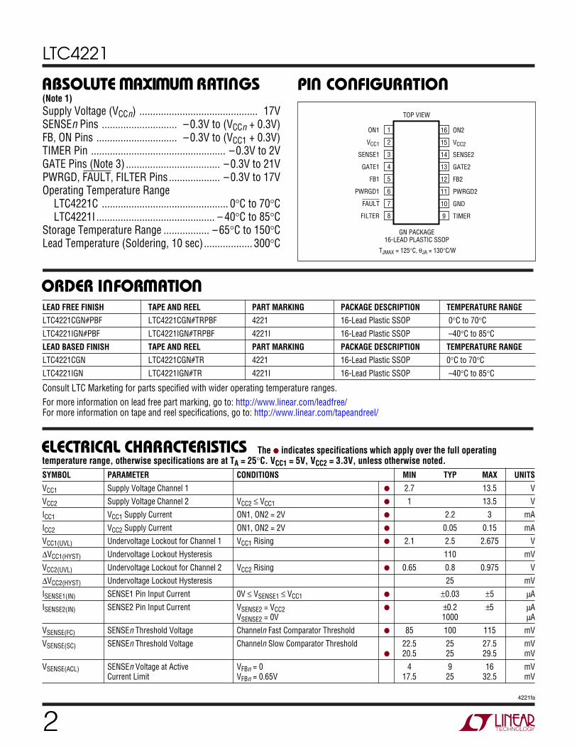
(Note 1)Supply Voltage (VCCn) ............................................ 17VSENSEn Pins ............................ –0.3V to (VCCn + 0.3V)FB, ON Pins .............................. –0.3V to (VCC1 + 0.3V)TIMER Pin .................................................. –0.3V to 2VGATE Pins (Note 3) ................................... –0.3V to 21VPWRGD, FAULT, FILTER Pins ................... –0.3V to 17VOperating Temperature Range
LTC4221C ............................................... 0°C to 70°CLTC4221I ............................................ – 40°C to 85°C
Storage Temperature Range ................. –65°C to 150°CLead Temperature (Soldering, 10 sec).................. 300°C
TJMAX = 125°C, θJA = 130°C/W
ABSOLUTE MAXIMUM RATINGS
W WW U
SYMBOL PARAMETER CONDITIONS MIN TYP MAX UNITS
VCC1 Supply Voltage Channel 1 ● 2.7 13.5 VVCC2 Supply Voltage Channel 2 VCC2 ≤ VCC1 ● 1 13.5 V
ICC1 VCC1 Supply Current ON1, ON2 = 2V ● 2.2 3 mA
ICC2 VCC2 Supply Current ON1, ON2 = 2V ● 0.05 0.15 mAVCC1(UVL) Undervoltage Lockout for Channel 1 VCC1 Rising ● 2.1 2.5 2.675 V
ΔVCC1(HYST) Undervoltage Lockout Hysteresis 110 mV
VCC2(UVL) Undervoltage Lockout for Channel 2 VCC2 Rising ● 0.65 0.8 0.975 VΔVCC2(HYST) Undervoltage Lockout Hysteresis 25 mV
ISENSE1(IN) SENSE1 Pin Input Current 0V ≤ VSENSE1 ≤ VCC1 ● ±0.03 ±5 μA
ISENSE2(IN) SENSE2 Pin Input Current VSENSE2 = VCC2 ● ±0.2 ±5 μAVSENSE2 = 0V 1000 μA
VSENSE(FC) SENSEn Threshold Voltage Channeln Fast Comparator Threshold ● 85 100 115 mV
VSENSE(SC) SENSEn Threshold Voltage Channeln Slow Comparator Threshold 22.5 25 27.5 mV● 20.5 25 29.5 mV
VSENSE(ACL) SENSEn Voltage at Active VFBn = 0 4 9 16 mVCurrent Limit VFBn = 0.65V 17.5 25 32.5 mV
The ● indicates specifications which apply over the full operatingtemperature range, otherwise specifications are at TA = 25°C. VCC1 = 5V, VCC2 = 3.3V, unless otherwise noted.
GN PACKAGE16-LEAD PLASTIC SSOP
1
2
3
4
5
6
7
8
TOP VIEW
16
15
14
13
12
11
10
9
ON1
VCC1
SENSE1
GATE1
FB1
PWRGD1
FAULT
FILTER
ON2
VCC2
SENSE2
GATE2
FB2
PWRGD2
GND
TIMER
ELECTRICAL CHARACTERISTICS
LEAD FREE FINISH TAPE AND REEL PART MARKING PACKAGE DESCRIPTION TEMPERATURE RANGELTC4221CGN#PBF LTC4221CGN#TRPBF 4221 16-Lead Plastic SSOP 0°C to 70°C
LTC4221IGN#PBF LTC4221IGN#TRPBF 4221I 16-Lead Plastic SSOP –40°C to 85°C
LEAD BASED FINISH TAPE AND REEL PART MARKING PACKAGE DESCRIPTION TEMPERATURE RANGELTC4221CGN LTC4221CGN#TR 4221 16-Lead Plastic SSOP 0°C to 70°C
LTC4221IGN LTC4221IGN#TR 4221I 16-Lead Plastic SSOP –40°C to 85°C
Consult LTC Marketing for parts specified with wider operating temperature ranges.
ORDER I FOR ATIOU UW
PI CO FIGURATIO
UUU
For more information on lead free part marking, go to: http://www.linear.com/leadfree/For more information on tape and reel specifications, go to: http://www.linear.com/tapeandreel/

3
LTC4221
4221fa
SYMBOL PARAMETER CONDITIONS MIN TYP MAX UNITS
IGATE(UP) GATEn Output Current VON1 = VON2 = 2V, VGATEn = 0V ● –7 –9.5 –12 μA
IGATE(DN) GATEn Output Current VON1 = VON2 = 0.6V, VGATEn = 3.3V ● 75 100 125 μAIGATE(FSTDN) GATEn Output Current UVLO with VGATEn = 3.3V or FAULT 16 mA
Latched with VGATEn = 3.3V
ΔVGATE External N-Channel Gate Drive VGATEn – VCC1 for VCC1 = 2.7V, VCC2 = 1V ● 4.5 13 VVGATEn – VCC1 for VCC1 = 3.3V, VCC2 = 2.5V ● 5 16 VVGATEn – VCC1 for VCC1 = 5V, VCC2 = 3.3V ● 8 16 VVGATEn – VCC1 for VCC1 = 12V, VCC2 = 12V ● 7 18 V
VGATE(OV) GATEn Overvoltage Lockout Threshold ● 0.4 0.5 VION(IN) ONn Pin Input Current 0V ≤ VONn ≤ VCC1 ● ±0.01 ±1 μA
VON(RESET) ON1 Reset Threshold VON1 Falling ● 0.375 0.4 0.425 V
ΔVON(RESETHYST) ON1 Reset Threshold Hysteresis 25 mV VON(OFF) ONn Off Threshold High to Low, GATEn Turns Off by 100μA ● 0.796 0.821 0.846 V
Pull-Down
ΔVON(OFFHYST) ONn Off Threshold Hysteresis 30 mV
IFB(IN) FBn Input Current 0V ≤ VFBn ≤ VCCn ● ±0.01 ±1 μA
VFB(UV) FBn Undervoltage Threshold FBn Falling ● 0.605 0.617 0.629 V
ΔVFB(UVHYST) FBn Undervoltage Threshold Hysteresis 3 mV
ΔVFB(LREG) FBn Threshold Line Regulation 2.7V ≤ VCC1 ≤ 13.5V 2 mV
VFB(OV) FBn Overvoltage Threshold FBn Rising ● 0.805 0.822 0.838 V
IFILTER(UP) FILTER Pull-Up Current During Current Fault Condition ● –80 –105 –132 μA
IFILTER(DN) FILTER Pull-Down Current During Normal Cycle ● 1.15 1.8 2.45 μA
VFILTER(TH) FILTER Threshold Latched Off Threshold, FILTER Rising ● 1.18 1.24 1.30 V
ΔVFILTER(HYST) FILTER Threshold Hysteresis 105 mV
ITMR(UP1) TIMER Pull-Up Current 1 Initial Timing Cycle ● –1.2 –1.9 –2.6 μA
ITMR(UP2) TIMER Pull-Up Current 2 Start-Up Cycle ● –15 –20 –25 μA
ITMR(FSTDN) TIMER Pull-Down Current VTIMER = 1.5V, End of Initial Timing Cycle 9 mA
VTMR(H) TIMER High Threshold TIMER Rising ● 1.172 1.234 1.27 V
VTMR(L) TIMER Low Threshold TIMER Falling ● 0.1 0.4 0.5 V
IFAULT(UP) FAULT Pull-Up Current ● –2.5 –3.8 –5 μA
VFAULT(TH) FAULT Threshold FAULT Falling ● 0.791 0.816 0.841 V
ΔVFAULT(HYST) FAULT Hysteresis 35 mV
VFAULT(OL) FAULT Output Low Voltage IFAULT = 1.6mA, VCC1 = 5V ● 0.14 0.4 V
IPWRGD(LK) PWRGDn Leakage Current VPWRGDn = VCC1, VFBn = 0.7V, Normal Cycle ● ±0.01 ±10 μA
VPWRGD(OL) PWRGDn Output Low Voltage IPWRGDn = 1.6mA, VCC1 = 5V, VFBn = 0V, ● 0.14 0.4 VNormal Cycle
tP(FC-GATE) Fast Comparator Trip to GATEn VSENSEn = VCCn to (VCCn – 200mV) Step ● 1 1.5 μsDischarging
tP(SC-FAULT) Slow Comparator Trip to FILTER VSENSEn = VCCn to (VCCn – 50mV) Step. ● 15 35 μsHigh and FAULT Latched FILTER Open
The ● indicates specifications which apply over the full operatingtemperature range, otherwise specifications are at TA = 25°C. VCC1 = 5V, VCC2 = 3.3V, unless otherwise noted.ELECTRICAL CHARACTERISTICS

4
LTC4221
4221fa
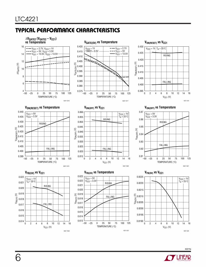
TYPICAL PERFOR A CE CHARACTERISTICS
UW
ICC1 vs Temperature
TEMPERATURE (°C)–50
I CC1
(mA)
4
5
6
25 75
4221 G01
3
2
–25 0 50 100 125
1
0
VCC2 = 1V
VCC1 = 13.5V
VCC1 = 12V
VCC1 = 5V
VCC1 = 2.7V
TEMPERATURE (°C)–50
I CC2
(mA)
0.175
25
4221 G02
0.100
0.050
–25 0 50
0.025
0
0.200
0.150
0.125
0.075
75 100 125
VCC1 = 13.5V
VCC2 = 13.5V
VCC2 = 12V
VCC2 = 5V
VCC2 = 3.3V
VCC2 = 1V
TEMPERATURE (°C)–50
V CC1
(UVL
) (V)
2.50
25
4221 G03
2.44
2.40
–25 0 50
2.38
2.36
2.52
2.48
2.46
2.42
75 100 125
TIMER = 0.3V
RISING
FALLING
ICC2 vs Temperature VCC1(UVL) vs Temperature
VCC2(UVL) vs Temperature |ISENSE2(IN)| vs VSENSE2 VSENSE(FC) vs VCC1
TEMPERATURE (°C)–50
0.770
V CC2
(UVL
) (V)
0.775
0.785
0.790
0.795
50
0.815
4221 G04
0.780
0–25 75 10025 125
0.800
0.805
0.810TIMER = 0.3V
RISING
FALLING
VSENSE2 (V)0
|I SEN
SE2(
IN)|
(μA)
1000
6
4221 G05
1
0.01
2 4 8
0.001
0.0001
10000
100
10
0.1
10 12
VCC1 = 2.7V, VCC2 = 1VVCC1 = 5V, VCC2 = 3.3VVCC1 = 13.5V, VCC2 = 13.5V
VCC1 (V)0
V SEN
SE(F
C) (m
V) 101.0
101.5
102.0
6 10 16
4221 G06
100.5
100.0
99.52 4 8 12 14
VCC2 = VCC1TA = 25°C
Note 1: Absolute Maximum Ratings are those values beyond which the lifeof the device may be impaired.Note 2: All current into device pins are positive. All voltages are referencedto ground unless otherwise specified.
Note 3: An internal zener on each GATE pin clamps the charge pumpvoltage to a typical maximum operating voltage of 26V. External overdriveof either GATE pin beyond its internal zener voltage may damage thedevice.
The ● indicates specifications which apply over the full operatingtemperature range, otherwise specifications are at TA = 25°C. VCC1 = 5V, VCC2 = 3.3V, unless otherwise noted.ELECTRICAL CHARACTERISTICS
SYMBOL PARAMETER CONDITIONS MIN TYP MAX UNITS
tP(FAULT-GATE) FAULT Low to GATEn Discharging VFAULT = 3.3V to 0V ● 15 35 μs
tP(OV-GATE) FBn OV Comparator Trip to GATEn VFBn = 0V to 1V ● 18 35 μsDischarging
tP(FILTER-GATE) Filter Comparator Trip to GATEn VFILTER = 0V to 1.5V ● 15 35 μsDischarging
tRESET Circuit Breaker Reset Delay Time VON1 < 0.4V to FAULT High ● 15 30 μs
tP(ON-GATE) Turn Off Propagation Delay VONn ≤ 0.821V to GATEn Discharging ● 15 35 μs

5
LTC4221
4221fa
TYPICAL PERFOR A CE CHARACTERISTICS
UW
VSENSE(ACL) vs VFB IGATE(UP) vs Temperature IGATE(DN) vs Temperature
IGATE(FSTDN) vs Temperature ΔVGATEn (VGATEn – VCC1) vs VCC1
VFB (V)0
V SEN
SE(A
CL) (
mV) 20
25
30
0.3 0.5
4221 G10
15
10
0.1 0.2 0.4 0.6 0.7
5
0
VCC1 = 5VVCC2 = 3.3VTA = 25°C
TEMPERATURE (°C)–50
I GAT
E(UP
) (μA
) –8
–7
–6
25 75
4221 G11
–9
–10
–25 0 50 100 125
–11
–12
VCC1 = 2.7VVCC1 = 5VVCC1 = 13.5V
VCC2 = 1VVGATE = 0V
TEMPERATURE (°C)–50
101
102
104
25 75
4221 G12
100
99
–25 0 50 100 125
98
97
103
I GAT
E(DN
) (μA
)
VCC1 = 2.7VVCC1 = 5VVCC1 = 13.5V
VCC2 = 1VVGATE = 3.3V
TEMPERATURE (°C)–50
I GAT
E(FS
TDN)
(mA) 40
50
60
25 75
4221 G13
30
20
–25 0 50 100 125
10
0
VCC1 = 2.7VVCC1 = 5VVCC1 = 13.5V
VCC2 = 1VVGATE = 3.3V
VCC1 (V)0
6
V GAT
En (V
)
7
9
10
11
8
15
4221 G14
8
42 10 126 14
12
13
14VCC2 = VCC1 – 1.5VTA = 25°C
ΔVGATE1
ΔVGATE2
ΔVGATE1 (VGATE1 – VCC1)vs Temperature
TEMPERATURE (°C)–50
12
14
18
25 75
4221 G15
10
8
–25 0 50 100 125
6
4
16
ΔVGA
TE1
(V)
VCC1 = 2.7V, VCC2 = 1VVCC1 = 5V, VCC2 = 3.3VVCC1 = 13.5V, VCC2 = 13.5V
VSENSE(FC) vs Temperature VSENSE(SC) vs VCC1 VSENSE(SC) vs Temperature
TEMPERATURE (°C)–50
V SEN
SE(F
C) (m
V) 101.0
101.5
102.0
25 75
4221 G07
100.5
100.0
–25 0 50 100 125
99.5
99.0
VCC1 = 5VVCC2 = 3.3V
VCC1 (V)0
V SEN
SE(S
C) (m
V)
25.0
25.2
25.4
12
4221 G08
24.8
24.6
4 82 146 10 16
24.4
24.2
25.6VCC2 = VCC1TA = 25°C
TEMPERATURE (°C)–50
V SEN
SE(S
C) (m
V)
25.8
25
4221 G09
25.2
24.8
–25 0 50
24.6
24.4
26.0
25.6
25.4
25.0
75 100 125
VCC1 = 5VVCC2 = 3.3V
6
LTC4221
4221fa
TYPICAL PERFOR A CE CHARACTERISTICS
UW
VON(RESET) vs Temperature VON(OFF) vs VCC1 VON(OFF) vs Temperature
TEMPERATURE (°C)–50
0.395
V ON(
RESE
T) (V
)
0.405
0.410
0.415
50
0.440
4221 G19
0.400
0–25 75 10025 125
0.425
0.420
0.430
0.435VCC1 = 5VVCC2 = 3.3V
RISING
FALLING
VCC1 (V)0
V ON(
OFF)
(V)
0.840
0.845
0.850
16
4221 G20
0.835
0.830
0.8154 8 122 6 10 14
0.825
0.820
0.860
0.855VCC2 = 1VTA = 25°C
RISING
FALLING
TEMPERATURE (°C)–50
V ON(
OFF)
(V) 0.85
0.86
0.87
25 75
4221 G21
0.84
0.83
–25 0 50 100 125
0.82
0.81
VCC1 = 5VVCC2 = 3.3V
RISING
FALLING
VFB(UV) vs VCC1 VFB(UV) vs Temperature VFB(OV) vs VCC1
VCC1 (V)0
V FB(
UV) (
V)
0.618
0.620
16
4221 G22
0.616
0.6144 8 122 6 10 14
0.622
0.617
0.619
0.615
0.621
VCC2 = 1VTA = 25°C
RISING
FALLING
TEMPERATURE (°C)–50
V FB(
UV) (
V)
0.623
0.622
0.621
0.620
0.619
0.618
0.617
0.616
0.615
0.614
0.6130 50 75
4221 G23
–25 25 100 125
VCC1 = 5VVCC2 = 3.3V
RISING
FALLING
VCC1 (V)0
V FB(
OV) (
V) 0.8210
0.8215
0.8220
12
4221 G24
0.8205
0.8200
4 82 146 10 16
0.8195
0.8190
0.8225VCC2 = 1VTA = 25°C
VGATE(OV) vs Temperature VON(RESET) vs VCC1
ΔVGATE2 (VGATE2 – VCC1)vs Temperature
TEMPERATURE (°C)–50
ΔVGA
TE2
(V) 12
14
16
25 75
4221 G16
10
8
–25 0 50 100 125
6
4
VCC1 = 2.7V, VCC2 = 1VVCC1 = 5V, VCC2 = 3.3VVCC1 = 13.5V, VCC2 = 13.5V
TEMPERATURE (°C)–50
0.375
V GAT
E(OV
) (V)
0.385
0.390
0.395
50
0.420
4221 G17
0.380
0–25 75 10025 125
0.405
0.400
0.410
0.415VCC1 = 2.7VVCC1 = 5VVCC1 = 13.5V
VCC2 = 1VTIMER = 0.5V
VCC1 (V)0
V ON(
RESE
T) (V
)
0.415
0.420
0.425
12
4221 G18
0.410
0.405
4 82 146 10 16
0.400
0.395
0.430VCC2 = 1V, TA = 25°C
FALLING
RISING

7
LTC4221
4221fa
TYPICAL PERFOR A CE CHARACTERISTICS
UW
VFILTER(TH) vs Temperature ITMR(UP1) vs Temperature
TEMPERATURE (°C)–50
V FIL
TER(
TH) (
V)
1.246
1.244
1.242
1.240
1.238
1.236
1.234
1.232
1.230
1.228
1.226
1.2240 50 75
4221 G28
–25 25 100 125
VCC1 = 2.7VVCC1 = 5VVCC1 = 13.5V
VCC2 = 1VVGATE1 = 0.2V
TEMPERATURE (°C)–50
I TM
R(UP
1) (μ
A)
–1.8
–1.7
–1.6
25 75
4221 G29
–1.9
–2.0
–25 0 50 100 125
–2.1
–2.2
VCC1 = 2.7VVCC1 = 5VVCC1 = 13.5V
VCC2 = 1VVTMR = 0.25V
ITMR(UP2) vs Temperature
TEMPERATURE (°C)–50
I TM
R(UP
2) (μ
A)
–17.0
–17.5
–18.0
–18.5
–19.0
–19.5
–20.0
–20.5
–21.0
–21.5
–22.00 50 75
4221 G30
–25 25 100 125
VCC1 = 2.7VVCC1 = 5VVCC1 = 13.5V
VCC2 = 1VVTMR = 0.25V
ITMR(FSTDN) vs Temperature VTMR(H) vs Temperature
TEMPERATURE (°C)–50 –25
0
I TM
R(FS
TDN)
(mA)
10
25
0 50 75
4221 G31
5
20
15
25 100 125
VCC1 = 2.7VVCC1 = 5VVCC1 = 13.5V
VCC2 = 1VVTMR = 1.5V
TEMPERATURE (°C)–50
V TM
R(H)
(V)
1.240
1.238
1.236
1.234
1.232
1.230
1.228
1.226
1.224
1.222
1.2200 50 75
4221 G32
–25 25 100 125
VCC1 = 2.7VVCC1 = 5VVCC1 = 13.5V
VCC2 = 1V
VTMR(L) vs Temperature
TEMPERATURE (°C)–50
V TM
R(L)
(V)
0.403
25
4221 G33
0.400
0.398
–25 0 50
0.397
0.396
0.404
0.402
0.401
0.399
75 100 125
VCC1 = 2.7VVCC1 = 5VVCC1 = 13.5V
VCC2 = 1V
VFB(OV) vs Temperature IFILTER(UP) vs Temperature
TEMPERATURE (°C)–50
V FB(
OV) (
V)
0.825
0.824
0.823
0.822
0.821
0.820
0.819
0.818
0.817
0.816
0.8150 50 75
4221 G25
–25 25 100 125
VCC1 = 5VVCC2 = 3.3V
TEMPERATURE (°C)–50
I FIL
TER(
UP) (
μA) –98
–93
–88
25 75
4221 G26
–103
–108
–25 0 50 100 125
–113
–118
VCC1 = 2.7VVCC1 = 5VVCC1 = 13.5V
VCC2 = 1VVFILTER = 1V
IFILTER(DN) vs Temperature
TEMPERATURE (°C)–50
1.85
1.90
2.00
25 75
4221 G27
1.80
1.75
–25 0 50 100 125
1.70
1.65
1.95
I FIL
TER(
DN) (
μA)
VCC1 = 2.7VVCC1 = 5VVCC1 = 13.5V
VCC2 = 1VVFILTER = 1V
8
LTC4221
4221fa
UUU
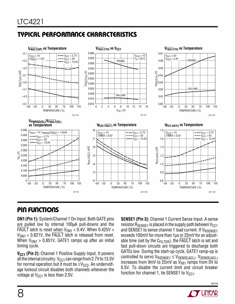
PI FU CTIO SON1 (Pin 1): System/Channel 1 On Input. Both GATE pinsare pulled low by internal 100μA pull-downs and theFAULT latch is reset when VON1 < 0.4V. When 0.425V <VON1 < 0.821V, the FAULT latch is released from reset.When VON1 > 0.851V, GATE1 ramps up after an initialtiming cycle.
VCC1 (Pin 2): Channel 1 Positive Supply Input. It powersall the internal circuitry. VCC1 can range from 2.7V to 13.5Vfor normal operation but it must be ≥VCC2. An undervolt-age lockout circuit disables both channels whenever thevoltage at VCC1 is less than 2.5V.
SENSE1 (Pin 3): Channel 1 Current Sense Input. A senseresistor RSENSE1 is placed in the supply path between VCC1and SENSE1 to sense channel 1 load current. If VRSENSE1exceeds 100mV for more than 1μs or 25mV for an adjust-able time (set by the CFILTER), the FAULT latch is set andfast pull-down circuits are triggered to discharge bothGATEs low. During the start-up cycle, GATE1 ramp-up iscontrolled to servo VRSENSE1 ≤ VSENSE(ACL). VSENSE(ACL)increases from 9mV to 25mV as VFB1 ramps from 0V to0.5V. To disable the current limit and circuit breakerfunction for channel 1, tie SENSE1 to VCC1.
TYPICAL PERFOR A CE CHARACTERISTICS
UW
VPWRGD(OL)/VFAULT(OL)vs Temperature tp(SC-FAULT) vs Temperature
TEMPERATURE (°C)–50
V OL
(V)
0.500
0.450
0.400
0.350
0.300
0.250
0.200
0.150
0.100
0.050
00 50 75
4221 G37
–25 25 100 125
VCC1 = 2.7VVCC1 = 5VVCC1 = 13.5V
VCC2 = 1V, IPWRGD/IFAULT = 1.6mA
tp(FC-GATE) vs Temperature
TEMPERATURE (°C)–50
tp(S
C-FA
ULT)
(μS) 16
17
18
25 75
4221 G38
15
14
–25 0 50 100 125
13
12
VCC1 = 2.7VVCC1 = 5VVCC1 = 13.5V
VCC2 = 1VTIMER = 0.5V
TEMPERATURE (°C)–50
tp(F
C-GA
TE) (
μS) 1.4
1.6
1.8
25 75
4221 G39
1.2
1.0
–25 0 50 100 125
0.8
0.6
VCC1 = 2.7VVCC1 = 5VVCC1 = 13.5V
VCC2 = 1VTIMER = 0.5V
IFAULT(UP) vs Temperature VFAULT(TH) vs VCC1 VFAULT(TH) vs Temperature
TEMPERATURE (°C)–50
–3.7
–3.5
–3.1
25 75
4221 G34
–3.9
–4.1
–25 0 50 100 125
–4.3
–4.5
–3.3
I FAU
LT(U
P) (μ
A)
VCC1 = 2.7VVCC1 = 5VVCC1 = 13.5V
VCC2 = 1VVFAULT = 1.5V
VCC1 (V)0
0.810
V FAU
LT(T
H) (V
)
0.815
0.825
0.830
0.835
0.860
0.845
4 8 10
4221 G35
0.820
0.850
0.855
0.840
2 6 12 14 16
VCC2 = 1VTA = 25°C
RISING
FALLING
TEMPERATURE (°C)–50
0.84
0.85
0.87
25 75
4221 G36
0.83
0.82
–25 0 50 100 125
0.81
0.80
0.86
V FAU
LT(T
H) (V
)
VCC1 = 5VVCC2 = 3.3V RISING
FALLING

9
LTC4221
4221fa
UUU
PI FU CTIO SGATE1 (Pin 4): Channel 1 Gate Drive. This pin is the highside gate drive of an external N-channel MOSFET. WhenVON1 < 0.821V, GATE1 is held low by a 100μA currentsource. When VON1 > 0.851V, an initial timing cycle isfollowed by a start-up cycle when an internal charge pumpprovides a 9.5μA pull-up to ramp up GATE1 with inrushcurrent limiting. UVLO, overvoltage, overcurrent and ex-ternally generated faults override the ON1 pin and pullGATE1 low.
FB1 (Pin 5): VOUT1 Feedback Input. FB1 monitors thechannel 1 output voltage with an external resistive divider.When VFB1 < 0.617V, the PWRGD1 pin is pulled low. WhenVFB1 > 0.822V, overvoltage is detected, the FAULT latch isset and both GATEs are pulled low. The FB1 pin is also usedto control the channel 1 current limit during its start-upcycle.
PWRGD1 (Pin 6): Channel 1 Power Good Output. PWRGD1is pulled low when VFB1 < 0.617V, during the initial timingcycle or when the chip is in UVLO. An external pull-up isrequired to generate a logic high at the open-drain PWRGD1pin.
FAULT (Pin 7): Fault Status Input/Output. FAULT is abidirectional pin. As an input, pulsing VFAULT < 0.816V willset the FAULT latch and bring the LTC4221 into the faultstate. As an output, FAULT is pulled high by an internal3.8μA pull-up under normal operating conditions. Whenan overcurrent fault is detected by a SENSE pin or aovervoltage fault detected by an FB pin, the FAULT latch isset and the LTC4221 goes into the fault state. The FAULTlatch is reset by a UVLO or the ON1 pin being driven below0.4V.
FILTER (Pin 8): Overcurrent Fault Timing Filter. TheFILTER pin requires an external capacitor to ground toadjust the response time of the two slow comparators. TheFILTER pin can be left unconnected for a default slowcomparator response time of 15μs.
TIMER (Pin 9): Analog System Timer. The TIMER pinrequires an external capacitor to ground to generatetiming delay cycles during start-up. The LTC4221’s initialand start-up timing cycles are controlled by CTIMER and theinternal current sources connected to the TIMER pin.
GND (Pin 10): Ground. Connect to a ground plane foroptimum performance.
PWRGD2 (Pin 11): Channel 2 Power Good Output. Similarfunctionality as PWRGD1. Controlled by FB2.
FB2 (Pin 12): VOUT2 Feedback Input. Similar functionalityas FB1. Monitors channel 2 output voltage, controlsPWRGD2 output and channel 2 start-up current limit.
GATE2 (Pin 13): Channel 2 Gate Drive. Similar functional-ity as GATE1. Controls the gate drive of the channel 2external N-channel MOSFET. ON2 controls GATE2 in thesame manner as ON1 controls GATE1. VON1 < 0.4V over-rides conditions at ON2 and GATE2 is held low by a 100μAcurrent source. UVLO, overvoltage, overcurrent and exter-nally generated faults override conditions at ON1 and ON2,and pull GATE2 low.
SENSE2 (Pin 14): Channel 2 Current Sense Input. Similarfunctionality as SENSE1. Monitors channel 2 load currentthrough RSENSE2 placed in the supply path between VCC2and SENSE2. To disable the current limit and circuitbreaker function for channel 2, tie SENSE2 to VCC2.
VCC2 (Pin 15): Channel 2 Positive Supply Input. VCC2 canrange from 1V to 13.5V for normal operation but it mustbe ≤VCC1. An undervoltage lockout circuit disables bothchannels whenever the voltage at VCC2 is less than 0.8V.
ON2 (Pin 16): Channel 2 On Input. GATE2 is pulled toground by a 100μA current source when VON2 < 0.821V.When VON2 > 0.851V, GATE2 ramps up after an initialtiming cycle.

10
LTC4221
4221fa
BLOCK DIAGRA
W
26V
9.5μA
100μA
CPO2
VCC2
CUR_LIMIT2
FPD2
+–
CHARGEPUMP 1
CHARGEPUMP 2
UVLOOSCILLATOR
VCC1
VCC1
VCC2
CPO1
CPO2
0.821VON1
COMPARATOR
SYSTEMCONTROL
LOGIC
0.4V
VCC1
1ON1
+–
ON2COMPARATOR
FILTERCOMPARATOR
TMRHICOMPARATOR
FAULTCOMPARATOR
0.821V
FTRHI
TMRHI
TIMER
1.234V
FAULT_LO
105μA
1.8μA
+
– +
–
1.24V
0.816V +
–
0.617V +
–
OV1COMPARATOR
FB1COMPARATOR
0.822V
+
–
16 9ON2
8FILTER
VCC1
3.8μA
VCC1
VCC1
FAULT 7 GND10
GATE1
26V
PWRGD1
CHANNEL ONE
20μA 1.9μA
VCC1 VCC1
9.5μA12V
12V
100μA
CPO1
VCC1
CUR_LIMIT1
FPD1
TMRLOCOMPARATOR
TMRLO 0.4V+
–
+
– SLOWCOMPARATOR 1
CHANNEL 1CONTROL
LOGIC
SLOWHI1
9mV TO 25mV
FASTHI1
2VCC1
+
– FASTCOMPARATOR 1
GATELO1COMPARATOR
GATELO1 0.4V+
–
SENSE1
+–
VCC1
100mV +–
3
FB1 5
6
4
0.617V +
–
OV2COMPARATOR
FB2COMPARATOR
0.822V
+
–
VCC2GATE2
PWRGD2
4221 BDCHANNEL TWO
+
– SLOWCOMPARATOR 2
CHANNEL 2CONTROL
LOGIC
SLOWHI2
9mV TO 25mV
FASTHI2
15VCC2
+
– FASTCOMPARATOR 2
GATELO2COMPARATOR
GATELO2 0.4V+
–
SENSE2
+–
VCC2
100mV +–
14
FB2 12
11
13

11
LTC4221
4221fa
Hot Circuit Insertion
When circuit boards are inserted into a live backplane, thesupply bypass capacitors can draw huge transient cur-rents from the power bus as they charge. The flow ofcurrent may damage the connector pins and glitch thepower bus, causing other boards in the system to reset.
The LTC4221 is designed to turn on and off a circuitboard’s supply voltages in a controlled manner, allowinginsertion or removal without glitches or connector dam-age. The LTC4221 can reside on the backplane or on theremovable circuit board for hot insertion applications. Itcontrols the path between the backplane power bus andthe daughter board load with an external MOSFET switch.Both inrush control and short-circuit protection are pro-vided by the external MOSFET. Each LTC4221 controlstwo channels, each with its individual MOSFET for sup-plies from 1V to 13.5V.
Overview
The timing diagram in Figure 1 shows some typical wave-forms of the LTC4221. The VCC and GND pins receivepower through the longest connector pins and are the firstto connect when the board is inserted. During the under-voltage lockout (UVLO) state before time point 1, bothGATE pins are held low by internal N-channel MOSFETpull-downs, turning the external MOSFETs off. Once bothVCC pins are valid at time point 1, the LTC4221 enters intoa reset state as ON1 is below its reset threshold. At timepoint 2, ON1 clears its reset threshold and the device goesfrom the reset state to an off state. When either ON1 orON2 clears its off threshold, both GATE pins are < 0.4V andTIMER < 0.4V (time points 3 and 4), the TIMER pin sources1.9μA and an initial timing cycle starts. Any transition ofON1 and ON2 through their off thresholds will reset theinitial timing cycle. At time point 5, TIMER reaches its highthreshold and is pulled down by an internal N-channelMOSFET to its low threshold at time point 6. The LTC4221then checks that FILTER pin voltage is low and FAULT pinvoltage is high. If both conditions are met, the electroniccircuit breaker is armed. The channel 1 start-up timingcycle starts at time point 6 since ON1 has cleared its offthreshold and ON2 has not.
OPERATIOU
During the start-up cycle, TIMER sources 20μA and GATE1sources 9.5μA. As GATE1 ramps up, MOSFET1 starts toturn on and current flows through to charge up the loadcapacitance. As VOUT1 and FB1 ramp up, the load currentis monitored through the external SENSE1 resistor. Be-tween time points 7 and 8, the GATE1 9.5μA pull-up iscontrolled to servo the voltage across RSENSE1 to be lessthan the SENSE1 active current limit voltage, which has acomponent controlled by the FB1 voltage (see Applica-tions Information: Start-Up Cycle with Current Limit). Inthis way, inrush current is limited and MOSFET1 does notoverheat during the start-up cycle. When FB1 clears itsundervoltage threshold, PWRGD1 asserts high. At timepoint 9, TIMER reaches its high threshold and is pulleddown by an internal N-channel MOSFET to its low thresh-old at time point 10. Channel 1’s slow comparator is armedat time point 9 and enters a fault monitor mode, bringingthe channel 1 start-up cycle to an end.
At time point 10, ON2 voltage is monitored and since ON2has cleared its off threshold, the start-up timing cyclerepeats for channel 2. The inrush current is low and GATE2ramps up without need for current limiting. Channel 2’sslow comparator is armed at time point 11 and enters afault monitor mode, ending the channel 2 start-up cycle.
Overcurrent faults translate to an increase in either VRSENSE.At time point 13, VRSENSE1 > 25mV (slow comparatorthreshold). The 1.8μA pull-down on the FILTER changes toa 105μA pull-up. When the FILTER pin hits its threshold attime point 14, it triggers a fault state when FAULT islatched low and both GATE pins are pulled low by internalN-channel MOSFETs, turning off the external MOSFETs.As each channel output discharges, its FB pin goes belowthe undervoltage threshold and the PWRGD pin deasserts.Higher overcurrents when either VRSENSE > 100mV (fastcomparator threshold) for more than 1μs will trigger thesame condition. This fault state can only be cleared by aUVLO at either VCC pin or a hard reset at the ON1 pin, asat time point 15, when ON1 is pulled below its resetthreshold. The LTC4221 then reverts back to its reset stateas between time points 1 and 2.

12
LTC4221
4221fa
OPERATIOU
VCCn
TIMER
FAULT
FILTER
ON1VON(OFF) + ΔVON(OFFHYST)
VON(RESET) + ΔVON(RESETHYST)
VON(OFF)
VGATE(OV)
VON(OFF) + ΔVON(OFFHYST)ON2
GATE1
GATE2
SENSE1
SENSE2
VOUT1
VOUT2
PWRGD1
PWRGD2
UVLO OFF INITIAL TIMING
RESET
100μA
100μA
VCCn(UVL)
1
VCCn CLEARS VCCn(UVL)
ELECTRONIC CIRCUIT BREAKER ARMED, CHECK FILTER < VFILTER(TH), FAULT > VFAULT(TH) + ΔVFAULT(HYST)
ON1 > VON(RESET) + ΔVON(RESETHYST)
CHANNEL 1 SLOW COMPARATOR ARMED
ON2 > VON(OFF), + ΔVON(OFFHYST),CHECK GATE < VGATE(OV), TIMER < 0.4V
ON1 > VON(OFF) + ΔVON(OFFHYST),CHECK GATE < VGATE(OV), TIMER < 0.4V
2
CHANNEL 2 SLOW COMPARATOR ARMED
3 4 5 6 7 8 9 10 11 12 13 14 15
1.9μA
VTMR(H)
VTMR(L)
20μA 20μA
1.8μAVFILTER(TH)
105μA
VON1(RESET)
VGATE(OV)
9.5μA
9.5μA
25mV9mV
9mV
VSENSE(FC)VSENSE(SC)
FB1 > VFB(UV) + ΔVFB(HYST)FB1 < VFB(UV)
FB2 < VFB(UV)FB2 > VFB(UV) + ΔVFB(HYST)
CHANNEL 1START-UP
CHANNEL 2START-UP
NORMAL FAULT RESET
4221 F01
Figure 1. LTC4221 Operation

13
LTC4221
4221fa
APPLICATIO S I FOR ATIO
WU UU
Undervoltage Lockout
An internal undervoltage lockout (UVLO) occurs if eitherVCC supply is too low for normal operation. The LTC4221is kept in lockout mode in which the internal charge pumpsare off, the GATE pins, TIMER are held low by internalN-channel MOSFET pull-downs and the FAULT latch reset,cutting off both channels. VCC1 has a low-to-high UVLOthreshold of 2.5V with 110mV hysteresis. VCC2 has a low-to-high UVLO threshold of 0.8V with 25mV hysteresis.Both UVLOs have glitch filters that filter out dips that areless than 30μs, allowing for bus supply transients. Anadditional requirement for normal operation is VCC1 ≥VCC2.
ON Pin Functions
The ON1 pin serves as a global reset for the LTC4221. Ithas an internal reset comparator with a high-to-low thresh-old of 0.4V, a 25mV hysteresis and a high-to-low glitchfilter of 15μs. Pulling ON1 below this threshold will put theLTC4221 into a reset state in which the TIMER is pulled lowby an internal N-channel MOSFET pull-down, the GATEpins are pulled low by separate internal 100μA pull-downsand the FAULT latch resets. A low-to-high transition on theON1 pin past the reset threshold releases the reset on theFAULT latch and both channels go into an off state.
In addition to its global reset function, ON1 also serves asan on/off switch for channel 1. ON2 performs the samerole for channel 2. Both pins have an off comparator witha high-to-low threshold of 0.821V and 30mV hysteresis.With these, ON1 and ON2 can be used to force a simulta-neous or sequential power-up/power-down of the twochannels. A simultaneous power-up and power-down isshown in Figure 2b. Both VCC pins clear their respectiveUVLO at time point 1 and both channels enter reset state.When ON1 clears its reset threshold, either ON1 or ON2clears its off threshold, both GATEs < 0.4V and TIMER <0.4V (time point 2), an initial timing cycle starts. At timepoint 4, the initial timing cycle completes and the LTC4221checks that FILTER is low and FAULT is high. If bothconditions are met, it then monitors the voltage of ON1 andON2. As long as its ON pin has cleared its off threshold,each channel powers up regardless of the state of the otherchannel. Similarly, if its ON pin goes below its off thresh-old, each channel pulls its GATE pin down with an internal100μA pull-down and turns off its external MOSFET re-gardless of the state of the other channel. As the circuit inFigure 2a has its two ON pins shorted together, a simulta-neous power-up is programmed at time points 4 to 5 anda simultaneous power down is programmed between timepoints 7 and 8. The timing waveforms in Figure 3 show a
+VCC1ON1
SENSE1ON2
RF215k
LTC4221*GATE1
FB1
4221 F02a
4221 F02b
1
16
10
9CTIMER1μF
GND
TIMER
(2a) Circuit (2b) Timing Waveforms
RF156k
VOUT13.3V5AVOUT22.5V5A
Q1IRF7413
RSENSE10.004Ω
CLOAD1
Z1
Z1 = SMAJ10* ADDITIONAL DETAILS OMITTED FOR CLARITY
RX110Ω
CX1100nF
R110k
R210k
LONGVCC1
LONG
PCB EDGECONNECTOR
(MALE)
SHORT
BACKPLANECONNECTOR
(FEMALE)
LONGVCC2
DISCHARGEBY LOAD
1
VCCn
VOUTn
ONn
GATEn
UVLO INITIALTIMING
CHANNELSTART-UP
RESET STATE
TIMER
0.851V
1.234V
0.821V
9.5μA 100μA
VTH
20μA
2 3 4 5 6 7 8
NORMAL RESET
VCCn(UVL)
1.9μA
Figure 2. Simultaneous Power On/Off
14
LTC4221
4221fa
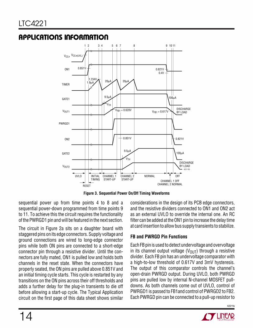
sequential power up from time points 4 to 8 and asequential power-down programmed from time points 9to 11. To achieve this the circuit requires the functionalityof the PWRGD1 pin and will be featured in the next section.
The circuit in Figure 2a sits on a daughter board withstaggered pins on its edge connectors. Supply voltage andground connections are wired to long-edge connectorpins while both ON pins are connected to a short-edgeconnector pin through a resistive divider. Until the con-nectors are fully mated, ON1 is pulled low and holds bothchannels in the reset state. When the connectors haveproperly seated, the ON pins are pulled above 0.851V andan initial timing cycle starts. This cycle is restarted by anytransitions on the ON pins across their off thresholds andadds a further delay for the plug-in transients to die offbefore allowing a start-up cycle. The Typical Applicationcircuit on the first page of this data sheet shows similar
considerations in the design of its PCB edge connectors,and the resistive dividers connected to ON1 and ON2 actas an external UVLO to override the internal one. An RCfilter can be added at the ON1 pin to increase the delay timeat card insertion to allow bus supply transients to stabilize.
FB and PWRGD Pin Functions
Each FB pin is used to detect undervoltage and overvoltagein its channel output voltage (VOUT) through a resistivedivider. Each FB pin has an undervoltage comparator witha high-to-low threshold of 0.617V and 3mV hysteresis.The output of this comparator controls the channel’sopen-drain PWRGD output. During UVLO, both PWRGDpins are pulled low by internal N-channel MOSFET pull-downs. As both channels come out of UVLO, control ofPWRGD1 is passed to FB1and control of PWRGD2 to FB2.Each PWRGD pin can be connected to a pull-up resistor to
0.821V
100μA
VCCn
1 2 3 4 5 6 7 8 9 10 11
ON1
TIMER
GATE1
VOUT1
PWRGD1
ON2
GATE2
UVLO INITIALTIMING
RESET
VOUT2
VCCn(UVL)
0.851V 0.821V0.4V
1.234V20μA
100μA
DISCHARGEBY LOAD
DISCHARGEBY LOAD
4221 F03
20μA
9.5μA
9.5μA
VTH
0.851V
VTH
VFB1 = 0.620V VFB1 = 0.617V
CHANNEL 1START-UP
CHANNEL 2START-UP CHANNEL 1 OFF
CHANNEL 2 NORMAL
NORMAL OFF
1.9μA
APPLICATIO S I FOR ATIO
WU UU
Figure 3. Sequential Power On/Off Timing Waveforms

15
LTC4221
4221fa
generate a logic high output to indicate that VOUT is valid.An internal high-to-low glitch filter helps to prevent nega-tive voltage transients on each FB pin from deasserting itsPWRGD. The relationship between glitch filter time and anFB pin transient voltage is shown in Figure 4. Using thefunctionality of the PWRGD1 pin, the LTC4221 can beconfigured to do sequential power-up and power-down asshown by the circuit in Figure 5. Referring back to Figure 3,ON2 is held low until VOUT1 ramps high enough for FB1 toexceed its undervoltage threshold at time point 5 whenPWRGD1 ramps up, pulling ON2 high. At time point 7, thecontrol logic sees ON2 exceeding its off threshold and socommences a start-up cycle for channel 2. Similarly, whenON1 is forced low by Q2 at time point 9, GATE1 is pulledlow by its 100μA pull-down while ON2 is held high by the
R4 pull-up on PWRGD1. Its is only when channel 1 ispowered off and VOUT1 discharges below its undervoltagethreshold at time point 10 that PWRGD1’s internalN-channel MOSFET pull-down is triggered and ON2 goeslow. At time point 11, ON2 trips its off threshold andGATE2 pulls low with a 100μA pull-down, powering offchannel 2.
For VOUT overvoltage detection, each FB pin has an over-voltage comparator with a low-to-high threshold of 0.822Vand a low-to-high glitch filter of 18μs. This threshold isdesigned to be 33% higher than the undervoltage thresh-old. If either FB pin trips this threshold, the fault latch is set,all GATE pins are pulled low with internal NFET pull-downsand the LTC4221 goes into a fault state.
In the third function, each FB pin is used to control itschannel’s current limit during its start-up cycle. This willbe featured in the Start-Up Cycle with Current Limitsection.
GATE Pin Functions
Each GATE pin controls the gate of its channel’s externalN-channel MOSFET. Individual internal charge pumpspowered by VCC1 guarantee a gate drive of minimum 4.5Vand maximum 18V (internally clamped) for GATE1 andGATE2. During UVLO, the internal charge pumps are offand both GATE pins are pulled low by internal N-channelMOSFET pull-downs. Outside UVLO, when ON1 is belowits off threshold, the charge pumps are on and GATE1 isheld low by an internal 100μA current pull-down. Once
APPLICATIO S I FOR ATIO
WU UU
+VCC1ON1
SENSE1ON2
PWRGD1
RF215k
LTC4221*GATE1
FB1
4221 F05
1
16
6
10
9CTIMER1μF
GND
TIMER
RF156k
VOUT13.3V5AVOUT22.5V5A
Q1IRF7413
RSENSE10.004Ω
CLOAD1
Z1
Q2: 2N7002LT1Z1: SMAJ10* ADDITIONAL DETAILS OMITTED FOR CLARITY
RX110Ω
CX1100nFR4
10kR22k
Q2 R110k
R610k
R5 10Ω
R3 10k
LONGVCC1
LONG
PCB EDGECONNECTOR
(MALE)
SHORT
SHORT
BACKPLANECONNECTOR
(FEMALE)
LONGVCC2
ON/OFF
Figure 5. Using PWRGD1 to Configure Sequential Power-Up/Power-Down
FEEDBACK TRANSIENT (mV)
GLIT
CH F
ILTE
R TI
ME
(μs)
40
60
80
20
50
70
30
10
00 20 40 60 80 100 120 140 160 180 200
4221 F04
TA = 25°C
Figure 4. FB Comparator Glitch FilterTime vs Feedback Transient Voltage

16
LTC4221
4221fa
ON1 clears its off threshold and the initial timing cycle iscomplete, the GATE1 pin is pulled up by a 9.5μA currentsource connected to the charge pump output during thechannel start-up cycle. GATE1 can be servoed by adjustingthe ramp up current to <9.5μA to control the inrushcurrent to the load during start-up. ON2 controls GATE2 ina similar manner but is overwritten by ON1’s global resetfunction. During an overcurrent fault condition that setsthe fault latch, both GATE pins are pulled down by theirrespective internal N-channel MOSFET pull-downs.
During hot insertion of the PCB, an abrupt application ofsupply voltage charges the external MOSFET drain/gatecapacitance. This can cause an unwanted gate voltagespike. An internal proprietary circuit holds both GATE pinslow before the internal circuitry wakes up. This reduces theMOSFET current surges substantially at insertion.
Electronic Circuit Breaker
The LTC4221 features an electronic circuit breaker func-tion that protects against supply overvoltage, externallygenerated fault conditions and shorts or excessive loadcurrent conditions on any of the supplies. If the circuitbreaker trips, both GATE pins are immediately pulled toground, the external N-channel MOSFETs are quicklyturned OFF and FAULT is latched low.
During the normal cycle, a supply overvoltage on channelnpropagates via the VOUTn resistive dividers to the FBn pin.A supply overvoltage high enough to pull either FB pinabove 0.822V for more than 18μs will trip the circuitbreaker.
The circuit breaker can also be made to trip by externallyforcing the bidirectional FAULT pin below 0.816V. TheFAULT pin has 35mV of hysteresis. An internal glitch filterof 15μs filters out noise on the FAULT pin.
The slow comparator of channeln trips the circuit breakerif VRSENSEn = (VCCn – VSENSEn) is greater than its 25mVthreshold for more than 15μs. There may be applicationswhere this inherent response time is not long enough, forexample, because of excessive supply voltage noise. Toadjust the response time of the slow comparator, a capaci-tor can be connected from the FILTER pin to GND. If thispin is left unused, each slow comparator’s delay defaultsto 15μs. During normal operation, the FILTER output pin
is held low by an internal 1.8μA pull-down current source.During an overcurrent condition on either channel asshown in Figure 6, the 1.8μA pull-down on the FILTER pinbecomes an internal 105μA pull-up and CFILTER chargesup. Once the FILTER pin voltage ramps past its low-to-high threshold of 1.24V at time point 2, the electroniccircuit breaker trips and the LTC4221 shuts down. TheFILTER pin’s internal 1.8μA pull-down discharges CFILTERand holds FILTER low. Each slow comparator’s responsetime from an overcurrent fault condition is:
tV C
AsFILTER
FILTER=μ
+ μ1 24105
15. •
(1)
Intermittent overloads may exceed the current limit as inFigure 7, but if the duration is sufficiently short, the FILTERpin may not reach the VFILTER(TH) threshold and theLTC4221 will not shut down. To handle this situation, theFILTER discharges with 1.8μA whenever both VRSENSE arebelow 25mV. Any intermittent overload with an aggregate
APPLICATIO S I FOR ATIO
WU UUFigure 7. Multiple Intermittent Overcurrent Condition
A1 B1 A2 B2 A3 B3
~25mV/RSENSE1
~25mV/RSENSE2
CIRCUIT BREAKERTRIPS
1.8μA
1.8μA
4221 F07
1.8μA
105μA105μA
105μA
ILOAD1
ILOAD2
VFILTER
VGATE
1.24V
1.8μA
SLOWCOMPARATOR
TRIPSLOW
COMPARATORTRIP
SLOWCOMPARATORTRIP
Figure 6. A Continuous Fault Timing
1.24V
1 2
NORMAL SLOW COMPARATOR
TRIP
VFILTER
CIRCUIT BREAKER TRIPS. GATE1, GATE2 ANDFAULT PULL LOW
1.8μA
1.8μA4221 F06
1.8μA105μA

17
LTC4221
4221fa
duty cycle of more than 1.8% will eventually trip the circuitbreaker. Figure 8 shows the circuit breaker response timein seconds normalized to 1μF. The asymmetric charging anddischarging of FILTER is a fair gauge of MOSFET heating.
tC F
VA D AFILTER μ( ) =
μ( ) μ1 24
105 1 8.• – . (2)
The fast comparators trip the circuit breaker to protectagainst fast load overcurrents if VRSENSE is greater thanVSENSE(FC) (100mV) for 1μs. The response time of each fastcomparator is fixed at 1μs nominal. The timing diagram inFigure 9 illustrates the operation of the LTC4221 when theload current conditions cause VRSENSE of channel 1 to ex-ceed 100mV for more than 1μs between time points 7 and8. Figure 9 also illustrates when the LTC4221’s electroniccircuit breaker is armed. After the initial timing cycle, it isarmed at time point 3. Arming the circuit breaker at timepoint 3 ensures that the system is protected against an over-current condition during the channel start-up cycle. At timepoint 4, the slow comparators are armed when the internalcontrol loop is disengaged.
Autoretry After a Fault
Once the LTC4221 circuit breaker is tripped, FAULT islatched low and both GATE pins are pulled to ground. Toclear the internal FAULT latch and to restart the LTC4221,its ON1 pin must be pulsed below its reset threshold(VON(RESET) = 0.4V) for at least 15μs.
APPLICATIO S I FOR ATIO
WU UU
TIMER
FAULT
FILTER
ONn0.851V
GATEn
SENSEn
VOUTn
RESET INITIAL TIMING
21
1.9μAVTMR(L)
VTMR(H)
ELECTRONIC CIRCUIT BREAKER ARMEDSLOW COMPARATORS ARMED
3
20μA20μA
1.8μA
0.4V
105μA
9.5μA
VFILTER(TH)
VSENSE(FC)VSENSE(SC)
4 5 6 7 8 9
RESET
4221 F09
CHANNELSTART-UP
NORMAL FAULT
Figure 9. Fast Comparator Trip Timing Waveforms
Figure 8. Circuit Breaker Filter Responsefor Intermittent Overload
OVERLOAD DUTY CYCLE, D (%)
NORM
ALIZ
ED R
ESPO
NSE
TIM
E (s
/μF)
1
0.01
0.1
0 10 20 30 40 50 60 70 80 90 1004221 F08
tCFILTER (μF)
1.24V105 • D – 1.8
=

18
LTC4221
4221fa
The LTC4221 can also be configured to automatically retryafter a fault condition. As shown in Figure 10, the FAULT(which has an internal 3.8μA pull-up current source) andboth ON pins are connected together. The timing diagramin Figure 11 illustrates a simultaneous start-up sequencewhere the LTC4221 is powered up into a load overcurrentcondition on channel 1. After the slow comparators are
armed at the end of the start-up cycle at time point 4, slowcomparator 1 immediately trips and FILTER ramps up.FILTER ramps past its high threshold at time point 6 andtrips the circuit breaker. FAULT and both ON pins arepulled low by an internal N-channel MOSFET and over-shoots below the 0.4V reset threshold of the ON1 pin.Once ON1 < 0.4V for more than 15μs, the internal fault
APPLICATIO S I FOR ATIO
WU UU
+VCC1ON1
SENSE1ON2
FAULT
RF215k
LTC4221*GATE1
FB1
4221 F10
1
16
7
10
9CTIMER1μF
GND
TIMER
RF156k
VOUT13.3V5AVOUT22.5V5A
Q1IRF7413
RSENSE10.004Ω
CLOAD1
8CFILTER
1nF
FILTER
Z1
Q2: 2N7002LT1Z1: SMAJ10* ADDITIONAL DETAILS OMITTED FOR CLARITY
RX110Ω
CX1100nF
CON10.47μF
R11M
LONGVCC1
LONG
PCB EDGECONNECTOR
(MALE)
SHORT
BACKPLANECONNECTOR
(FEMALE)
LONGVCC2
FAULT
Figure 10. Using FAULT to Configure Autoretry
21 3 4 5 6 7 8 9
20μA
ELECTRONIC CIRCUIT BREAKER ARMED
20μA 2μA
1.8μA
0.4V0.4V
0.851V
VFILTER(TH)
VSENSE(FC)
VSENSE(SC)
9.5μA
105μA
1.9μAVTMR(L)
VTMR(H)
0.851V
TIMER
ONn, FAULT
FILTER
GATE1
SENSE1
VOUT1
RESET CHANNELSTART-UP
FILTERRAMP
RESET
tON tINITIAL
OFF INITIALTIMING
4221 F11
INITIAL TIMING
tINITIAL tSTARTUP tFILTER
SLOW COMPARATORS ARMED
Figure 11. Autoretry Timing Waveforms

19
LTC4221
4221fa
latch is cleared and the FAULT pin sources a 3.8μA pull-upcurrent to charge up CON1. The typical delay tON is :
t V VC
AONON= ( )μ
0 851 0 43 8
1. – . •. (3)
As shown in the timing diagram of Figure 11, the autoretrycircuitry will attempt to restart the LTC4221 with a dutycycle:
Duty Cycle = tSTARTUP +( )+ + +
tt t t t
FILTER
ON INITIAL STARTUP FILTER
• %100(4)
tFILTER is defined in Equation 1 and tON is defined in Equa-tion 3. tINITIAL, the initial timing cycle delay, is given inEquation 9 located in the Initial Timing Cycle section.tSTARTUP, the start-up cycle delay, is given in Equation 10and found in the Start-Up Cycle Without Current Limitsection. Using the capacitor values as shown in Figure 10,the Autoretry Duty cycle works out to be approximately 6%.
Sense Resistor Consideration
The fault current level at which the LTC4221’s internalelectronic circuit breaker trips is determined by senseresistors connected between each channel’s VCC andSENSE pins. For both channels, the slow comparator tripcurrent and the fast comparator trip current are given byequations (5) and (6) respectively.
IV
RmV
RTRIP SCSENSE SC
SENSE SENSE( )
( )= = 25(5)
IV
RmV
RTRIP FCSENSE FC
SENSE SENSE( )
( )= = 100(6)
The power rating of the sense resistor should be rated atthe fault current level. Table 1 in the Appendix lists somecommon sense resistors.
For proper circuit breaker operation, Kelvin-sense PCBconnections between the sense resistor and each channel’sVCC and SENSE pins are strongly recommended. Thedrawing in Figure 12 illustrates the connections betweenthe LTC4221 and the sense resistor. PCB layout should bebalanced and symmetrical to minimize wiring errors. Inaddition, the PCB layout for the sense resistor should
include good thermal management techniques for optimalsense resistor power dissipation.
Calculating Current Limit
For a selected RSENSE, the load current must not exceedITRIP(SC). The minimum ITRIP(SC) is given by Equation 7:
IVR
mVRTRIP SCMIN
SENSE SCMIN
SENSE MAX SENSE MAX( )
( )
( ) ( )
.= = 20 5(7)
where
R RR
SENSE MAX SENSETOL
( ) •= +⎛⎝⎜
⎞⎠⎟
1100
The maximum ITRIP(SC) is given by Equation 8:
IVR
mVRTRIP SCMAX
SENSE SCMAX
SENSE MIN SENSE MIN( )
( )
( ) ( )
.= = 29 5(8)
where
R RR
SENSE MIN SENSETOL
( ) • –= ⎛⎝⎜
⎞⎠⎟
1100
If a 7mΩ sense resistor with ±1% tolerance is used forcurrent limiting, the nominal slow comparator trip currentis 3.57A. From Equations 7 and 8, ITRIP(SCMIN) = 2.9A andITRIP(SCMAX) = 4.26A. For proper operation, the minimumITRIP(SC) must exceed the circuit maximum operating loadcurrent. For reliability purposes, the operation at themaximum trip current must be evaluated carefully. Ifnecessary, two resistors with the same RTOL can beconnected in parallel to yield a nominal RSENSE value thatfits the circuit requirements.
APPLICATIO S I FOR ATIO
WU UU
SENSE RESISTOR
TOVCCn
TOSENSEn
CURRENT FLOWTO LOAD
CURRENT FLOWTO LOAD
TRACK WIDTH W:0.03" PER AMP
ON 1oz COPPERW
4221 F12
Figure 12. PCB Connections to the Sense Resistor

20
LTC4221
4221fa
Timer Function
The TIMER pin controls the initial cycle and the channelstart-up cycles with an external capacitor, CTIMER. Thereare two comparator thresholds: VTMR(H) (1.234V) andVTMR(L) (0.4V). In addition, the pin has a 1.9μA pull-upcurrent, a 20μA pull-up current and a N-channel MOSFETpull-down.
Initial Timing Cycle
When the card is being inserted into the bus connector, thelong pins mate first which brings up the supplies at timepoint 1 of Figure 13. The LTC4221 is in reset mode as theON1 pin is low. Both GATE pins and the TIMER pin arepulled low. At time point 2, the short pin makes contact andboth ON pins are pulled high. At this instant, a start-upcheck requires that both supply voltages be above UVLO,at least one ON pin be above 0.851V, both GATE pins< 0.4V and TIMER < 0.4V. When these four conditions arefulfilled, the initial cycle begins and the TIMER pin is pulledhigh with 1.9μA. At time point 3, the TIMER reachesVTMR(H) and is pulled down below VTMR(L) by the N-channel MOSFET pull-down, ending the initial cycle at timepoint 4. The initial cycle delay is:
t VC
AINITIALTIMER=
μ1 234
1 9. •
. (9)
At time point 4, the LTC4221 checks whether the FILTERpin is <1.24V and FAULT is > 0.851V. If both conditions aremet, a channel start-up cycle commences.
Start-Up Cycle Without Current Limit
During a channel start-up cycle, the TIMER pin ramps upwith a 20μA internal pull-up so the start-up cycle delay is:
t V VC
ASTARTUPTIMER= ( )
μ1 234 0 4
20. – . • (10)
At the beginning of the start-up timing cycle (time point 4),the LTC4221’s electronic circuit breaker is armed and eachchannel has an internal 9.5μA current source working withan internal charge pump to provide the gate drive to itsexternal pass transistor. At time point 5, GATE1 reachesthe external pass transistor threshold and VOUT1 starts tofollow the GATE1 ramp-up. If the inrush current is belowcurrent limit, GATE1 ramps at a constant rate of:
ΔΔ
=VT
IC
GATE GATE
GATE(11)
where CGATE is the total capacitance at the GATE1 pin. Theinrush current through RSENSE1 can be divided into twocomponents; ICLOAD due to the total load capacitanceCLOAD and ILOAD due to the noncapacitive load elements.The load bypass capacitance typically dominates CLOAD.For a successful channel start-up without current limit,IINRUSH < active current limit. Due to the voltage followerconfiguration, the VOUT1 ramp rate approximately tracksVGATE1. The inrush current during a start-up cycle withoutcurrent limit is :
I CV
TI
I CV
TI
I CIC
I
INRUSH LOADOUT
LOAD
INRUSH LOADGATE
LOAD
INRUSH LOADGATE
GATELOAD
= ΔΔ
⎛⎝⎜
⎞⎠⎟
+
= ΔΔ
⎛⎝⎜
⎞⎠⎟
+
= ⎛⎝⎜
⎞⎠⎟
+
•
•
•
(12)
At time point 6, VOUT1 is approximately VCC1 but GATE1ramp-up continues until it reaches a maximum voltage.This maximum voltage is determined either by the chargepump or the internal clamp.
APPLICATIO S I FOR ATIO
WU UU
1.234V
VCCn
VOUT1
ONn
TIMER
GATE1
RESETSTATE
INITIALTIMING
CHANNEL 1START-UP
NORMAL
20μA
9.5μA
0.4V
VTH
DISCHARGEBY LOAD
4221 F13
0.851V
0.4V
1 2 3 4 5 6 7
1.9μA
Figure 13. Channel 1 Start-Up Without Current Limit

21
LTC4221
4221fa
0.4V
VTH
1.234V1.9μA 20μA
<9.5μA9.5μA 9.5μA
DISCHARGEBY LOAD
4221 F14
0.851V
0.4V
1.234V
1 2
VCCn
VONn
VTIMER
VGATE2
VOUT2
IRSENSE2
3 4 5 6 7 8 9 A
REGULATED AT 25mV/RSENSEREGULATED AT
VSENSE(ACL)(t)/RSENSE
RESETSTATE
INITIALTIMING
CHANNEL 2START-UP
NORMALCYCLE
Start-Up Cycle With Current Limit
During a channel start-up cycle, if the inrush current asaccording to Equation (12) is large enough to cause avoltage drop greater than the active current limit threshold(VSENSE(ACL)) across the sense resistor, an internal servoloop controls the operation of the 9.5μA current source atthe GATE pin to regulate the load current to:
IV
RINRUSHSENSE ACL
SENSE= ( )
(13)
The active current limit threshold for channel n has acomponent controlled by the voltage at the FBn pin. WhenFBn = 0V, VSENSE(ACL) = 9mV. As VOUTn and FBn ramp up,VSENSE(ACL) increases linearly until FBn reaches 0.5V,where VSENSE(ACL) saturates at 25mV. In this fashion, theinrush current is controlled by this “foldback” limiting thattends to keep the power dissipation in the external MOSFETconstant during the start-up cycle.
The timing diagram in Figure 14 illustrates the operation ofthe LTC4221 in a channel start-up cycle with limited inrush
current as described by Equation 13. Between time points5 and 6, the GATE2 pin ramps up with IGATE = 9.5μA. Attime point 6, the inrush current increases enough to tripVSENSE(ACL)(t) and an internal servo loop engages, limitingthe inrush current to the level as in Equation 13 bydecreasing IGATE (<9.5μA). As a result, the ramp rate ofboth VGATE2 and VOUT2 decreases and VSENSE2 increaseslinearly until it saturates at 25mV at time point 7. At timepoint 8, the external MOSFET enters triode operation.IINRUSH drops as the ramp rate of VOUT2 falls below that ofVGATE2 so IGATE reverts back to 9.5μA. At time point 9, theinternal servo loop to control IINRUSH is disengaged andchannel 2 slow comparator is armed, ending the channel 2start-up cycle. So if CLOAD2 is not fully charged up at thispoint, IINRUSH will be subject to the slow comparatorthreshold and actions as outlined in the Electronic CircuitBreaker section. For a successful channel start-up, thecurrent limited part of the VOUT ramp-up (time points 6 and8 of Figure 14) must not exceed the sum of start-up cycledelay as given by Equation 10 and the slow comparatorresponse time as given by Equation 1. An example of anunsuccessful start-up is Figure 11 which shows a channelpowering up into an overcurrrent at the load.
The fast comparators of both channels are armed at theend of the initial timing cycle at time point 4 of Figure 14.If a short circuit during the start-up cycle overrides theservo loop and causes VRSENSE of either channel to exceed100mV for more than 1μs, the electronic circuit breakertrips and the LTC4221 enters the fault state.
Frequency Compensation at Start-Up Cycle
If a channel’s external gate input capacitance (CISS) isgreater than 600pF, no external gate capacitor is requiredat GATE to stabilize the internal current-limiting loop dur-ing start-up with current limit. The servo loop that controlsthe external MOSFET during current limiting has a unity-gain frequency of about 105kHz and phase margin of 80°for external MOSFET gate input capacitances to 2.5nF.
Power MOSFET
Power MOSFETs can be classified by RDS(ON) at VGS gatedrive ratings of 10V, 4.5V, 2.5V and 1.8V. Those rated forRDS(ON) at 10V VGS usually have a higher VGS absolutemaximum rating than those at 4.5V and 2.5V. At low
APPLICATIO S I FOR ATIO
WU UUFigure 14. Channel 2 Start-Up with Current Limit

22
LTC4221
4221fa
supply voltages, the LTC4221 can drive any MOSFET ratedwith 4.5V or 2.5V gate drive. For higher supply voltages upto 13.5V, the LTC4221 can drive any MOSFET rated witha 10V or 4.5V gate drive. The selected MOSFET shouldfulfill two VGS criteria:
1. Positive VGS absolute maximum rating > LTC4221’smaximum ΔVGATE.
2. Negative VGS absolute maximum rating > supply volt-age. The gate of the MOSFET can discharge faster thanVOUT when shutting down the MOSFET with a largeCLOAD.
If one of the conditions cannot be met, an external zenerclamp shown on Figure 15 can be used. The clampnetwork is connected from each channel’s GATE to theVOUT pins. VGS is clamped in both directions and RG limitsthe current flow into the GATEn pin’s internal zener clampduring transient events.
A MOSFET with a VGS absolute maximum rating of ±20Vmeets the two criteria for all the LTC4221 application rangesfrom 1V to 13.5V. Typically most 10V gate rated MOSFETshave VGS absolute maximum ratings of ±20V or greater, sono external VGS zener clamp is needed. There are 4.5V gaterated MOSFETs with VGS absolute maximum ratings of±20V. In addition to the MOSFET gate drive rating and VGSabsolute maximum rating, other criteria such as VBDSS,ID(MAX), RDS(ON), PD, θJA, TJ(MAX) and maximum safeoperating area (SOA) should also be carefully reviewed.VBDSS should exceed the maximum supply voltage inclu-sive of spikes and ringing. ID(MAX) must exceed the maxi-mum short-circuit current in the channel during a fault
condition. RDS(ON) determines the MOSFET VDS which to-gether with VRSENSE yields an error in the VOUT voltage. Forexample, at 1V VCC2, VDS + VRSENSE2 = 50mV gives a 5%VOUT2 error. At higher VCC voltages the VDS requirement canbe relaxed in which case the MOSFET’s thermal require-ments (PD, TJ(MAX), SOA) may limit the value of RDS(ON).
The power dissipated in the MOSFET is (ILOAD)2 • RDS(ON)and this should be less than the maximum power dissipa-tion, PD, allowed in that package. Given power dissipation,the MOSFET junction temperature, TJ can be computedfrom the operating temperature (TA) and the MOSFETpackage thermal resistance (θJA). The operating TJ shouldbe less than the TJ(MAX) specification. The VDS • ILOADfigure must also be well within the manufacturer’s recom-mended safe operating area (SOA) with sufficient margin.These three thermal parameters must not be exceeded forall conditions in a channel including normal mode opera-tion, start-up with or without current limit, fault andautoretry after a fault. To ensure a reliable design, faulttests should be evaluated in the laboratory.
VCC Transient Protection
Good engineering practice calls for bypassing the supplyrail of any analog circuit. Bypass capacitors are oftenplaced at the supply connection of every active device, inaddition to one or more large value bulk bypass capacitorsper supply rail. If power is connected abruptly, the largebypass capacitors slow the rate of rise of the supplyvoltage and heavily damp any parasitic resonance of leador PC track inductance working against the supply bypasscapacitors.
The opposite is true for LTC4221 Hot Swap circuitsmounted on plug-in cards since controlling the surgecurrent to bypass capacitors at plug-in is the primarymotivation for the Hot Swap controller. In most cases,there is no supply bypass capacitor present on the pow-ered supply voltage side of the MOSFET switch. Althoughwire harness, backplane and PCB trace inductances areusually small, these can create large spikes when largecurrents are suddenly drawn, cut off or limited. Abruptintervention can prevent subsequent damage caused by acatastrophic fault but it does cause a large supply tran-sient. These ringing transients appear as a fast edge on
APPLICATIO S I FOR ATIO
WU UU
*USER SELECTED VOLTAGE CLAMP(A LOW BIAS CURRENT ZENER DIODE IS RECOMMENDED)1N4688 (5V)1N4692 (7V): LOGIC-LEVEL MOSFET1N4695 (9V)1N4702 (15V): STANDARD-LEVEL MOSFET
RSENSE
GATE
4221 F15
Q1
RG200Ω
D1* D2*
VCC VOUT
Figure 15. Gate Protection Zener Clamp
23
LTC4221
4221fa
the input supply line, exhibiting a peak overshoot to 2.5times the steady-state value. This peak is followed by adamped sinusoidal response whose duration and periodare dependent on the resonant circuit parameters. Thiscan cause detrimental damage to board componentsunless measures are taken.
The energy stored in the lead/trace inductance is easilycontrolled with snubbers and/or transient voltage sup-pressors. Even when ferrite beads are used for electro-magnetic interference (EMI) control, the low saturatingcurrent of ferrite will not pose a major problem if thetransient voltage suppressors with adequate ratings areused. The transient associated with a GATE turn off can becontrolled with a snubber and/or transient voltage sup-pressor. Snubbers such as RC networks are effectiveespecially at low voltage supplies. The choice of RC isusually determined experimentally. The value of the snub-ber capacitor is usually chosen between 10 to 100 timesthe MOSFET COSS. The value of the snubber resistor istypically between 3Ω to 100Ω. When the supply exceeds7V or EMI beads exist in the wire harness, a transientvoltage suppressor and snubber are recommended to clipoff large spikes and reduce the ringing. For supply volt-ages of 6V or below, a snubber network should be suffi-cient to protect against transient voltages. These protectionnetworks should be mounted very close to each ofLTC4221’s two supply voltages using short lead lengths tominimize lead inductance. This is shown schematically inthe Typical Application on the front page of this data sheet.In many cases, a simple short-circuit test can be per-formed to determine the need of the transient voltagesuppressor. Additional overvoltage protection is providedby the FBn pins.
APPLICATIO S I FOR ATIO
WU UU
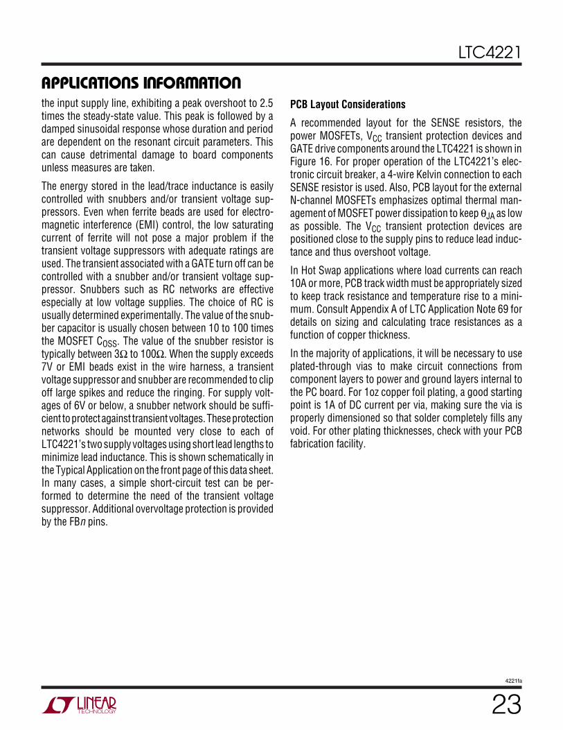
PCB Layout Considerations
A recommended layout for the SENSE resistors, thepower MOSFETs, VCC transient protection devices andGATE drive components around the LTC4221 is shown inFigure 16. For proper operation of the LTC4221’s elec-tronic circuit breaker, a 4-wire Kelvin connection to eachSENSE resistor is used. Also, PCB layout for the externalN-channel MOSFETs emphasizes optimal thermal man-agement of MOSFET power dissipation to keep θJA as lowas possible. The VCC transient protection devices arepositioned close to the supply pins to reduce lead induc-tance and thus overshoot voltage.
In Hot Swap applications where load currents can reach10A or more, PCB track width must be appropriately sizedto keep track resistance and temperature rise to a mini-mum. Consult Appendix A of LTC Application Note 69 fordetails on sizing and calculating trace resistances as afunction of copper thickness.
In the majority of applications, it will be necessary to useplated-through vias to make circuit connections fromcomponent layers to power and ground layers internal tothe PC board. For 1oz copper foil plating, a good startingpoint is 1A of DC current per via, making sure the via isproperly dimensioned so that solder completely fills anyvoid. For other plating thicknesses, check with your PCBfabrication facility.
24
LTC4221
4221fa
APPLICATIO S I FOR ATIO
WU UU
Figure 16. Recommended Layout for LTC4221 RSENSE, Power MOSFETs and Feedback Networks
G
W
•••••
•••••
POWER MOSFETSO-8
POWER MOSFETSO-8
NOTE: DRAWING IS NOT TO SCALE*ADDITIONAL DETAILS OMITTED FOR CLARITY
RSENSE2
RSENSE1
TRACK WIDTH W
CURRENT FLOWTO LOAD
CHANNEL 2OUTPUT
S
S
S
RF3
RF4
VIAS
BOTTOM LAYERAND GND TRACE
VIASGNDTO
LOAD
D
D
D
D
LTC4221*
G
S
S
S
D
D
D
D
16 15 14 13 12 11 10 9
1 2 3 4 5 6 7 8
ON1
V CC1
SENS
E1
GATE
1
FB1
PWRG
D1
FAUL
T
FILT
ER
ON2
V CC2
SENS
E2
GATE
2
FB2
PWRG
D2
GND
TIM
ER
RF2
RF1
4221 F16
R4
R3
R1CX1
R2
Z1
RX1
RX2
Z2
CX2
WCHANNEL 2INPUT
CHANNEL 1OUTPUT
CHANNEL 1INPUT
GND
CURRENT FLOWTO LOAD
CURRENT FLOWTO LOAD
CURRENT FLOWTO LOAD
W
CTIMER
CFILTER
APPE DIX
U
Table 1 lists some current sense resistors that can be usedwith the circuit breaker. Table 2 lists some power MOSFETsthat are available. Table 3 lists the web sites of several
manufacturers. Since this information is subject to change,please verify the part numbers with the manufacturer.
Table 1. Sense Resistor Selection GuideCURRENT LIMIT VALUE PART NUMBER DESCRIPTION MANUFACTURER
1A LRF120601R020F 0.02Ω 0.5W 1% Resistor IRC-TT
2.5A WSL25127L000F 0.007Ω 1W 1% Resistor Vishay-Dale
3.3A WSL25126L000F 0.006Ω 1W 1% Resistor Vishay-Dale
5A WSL25124L000F 0.004Ω 1W 1% Resistor Vishay-Dale
10A WSL25122L000F 0.002Ω 1W 1% Resistor Vishay-Dale
2A LRF120601R010F 0.01Ω 0.5W 1% Resistor IRC-TT

25
LTC4221
4221fa
TYPICAL APPLICATIO S
U
Simultaneous Turn-On with Autoretry Function—Individual Current Limits
ON2
FAULT
GND
LTC4221
Z1 Z2
1
16
7
10
9
8
FB2
PWRGD2
PWRGD1
PWRGD2
VOUT15V5AVOUT23.3V2.5A
PWRGD1
FB1
LONG
LONG
GNDLONG
Z1, Z2: SMAJ10TIMER
FILTER
2 3 4 15 14 13
12
11
6
5
ON1
VCC1 SENSE1 GATE1 VCC2 SENSE2 GATE2
VCC15V
VCC23.3V
BACKPLANECONNECTOR
(FEMALE)
PCB EDGECONNECTOR
(MALE)
RX110Ω
RX210Ω
R315k
R221k
R13.16k
RF320k
Q2IRF7413
RF45.11k
RPG210k
RPG110k
RF132.4k
RF25.11k
4221 TA02
CX1100nF
CFILTER1nF
CTIMER470nF
CX2100nF
Q1IRF7413
RSENSE10.004Ω
RSENSE20.007Ω
APPE DIX
U
Table 2. N-Channel Selection GuideCURRENT LEVEL (A) PART NUMBER DESCRIPTION MANUFACTURER
0 to 2 MMDF3N02HD Dual N-Channel SO-8 ON SemiconductorRDS(ON) = 0.1Ω, CISS = 455pF
2 to 5 MMSF5N02HD Single N-Channel SO-8 ON SemiconductorRDS(ON) = 0.025Ω, CISS = 1130pF
5 to 10 MTB50N06V Single N-Channel DD Pak ON SemiconductorRDS(ON) = 0.028Ω, CISS = 1570pF
10 to 20 MTB75N05HD Single N-Channel DD Pak ON SemiconductorRDS(ON) = 0.0095Ω, CISS = 2600pF
Table 3. Manufacturers’ Web SitesMANUFACTURER WEB SITE
TEMIC Semiconductor www.temic.com
International Rectifier www.irf.com
ON Semiconductor www.onsemi.com
Harris Semiconductor www.semi.harris.com
IRC-TT www.irctt.com
Vishay-Dale www.vishay.com
Vishay-Siliconix www.vishay.com
Diodes, Inc. www.diodes.com

26
LTC4221
4221fa
TYPICAL APPLICATIO S
U
Sequenced Turn-On
ON2
FAULT
GND
LTC4221
Z1 Z2
1
16
7
10
9
8
FB2
PWRGD2
PWRGD1
PWRGD2
VOUT13.3V5AVOUT22.5V5A
FB1
LONG
LONG
GNDLONG
Z1, Z2: SMAJ10TIMER
FILTER
2 3 4 15 14 13
12
11
6
5
ON1
VCC1 SENSE1 GATE1 VCC2 SENSE2 GATE2
VCC13.3V
VCC22.5V
BACKPLANECONNECTOR
(FEMALE)
PCB EDGECONNECTOR
(MALE)
RX110Ω
RX210Ω
R314.3k
R410k
R221k
R110k
RF314.3k
Q2IRF7413
RF45.11k
RPG210k
RF120k
RF25.11k
4221 TA04
CX1100nF
CFILTER1nF
CTIMER470nF
CX2100nF
Q1IRF7413
RSENSE10.004Ω
RSENSE20.004Ω
Simultaneous Turn-On with Autoretry Function—Linked Current Limits
ON2
FAULT
GND
LTC4221
Z1 Z2
1
16
7
10
9
8
FB2
PWRGD2
PWRGD1
PWRGD2
VOUT13.3V5AVOUT22.5V5A
PWRGD1
FB1
LONG
LONG
GNDLONG
Z1, Z2: SMAJ10TIMER
FILTER
2 3 4 15 14 13
12
11
6
5
ON1
VCC1 SENSE1 GATE1 VCC2 SENSE2 GATE2
VCC13.3V
VCC22.5V
BACKPLANECONNECTOR
(FEMALE)
PCB EDGECONNECTOR
(MALE)
RX110Ω
RX210Ω
R312.4k
R216.5k
R14.22k
RF314.3k
Q2IRF7413
RF45.11k
RPG210k
RPG110k
RF120k
RF25.11k
4221 TA03
CX1100nF
CFILTER1nF
CTIMER470nF
CX2100nF
Q1IRF7413
RSENSE10.004Ω
RSENSE20.004Ω
27
LTC4221
4221fa
U
PACKAGE DESCRIPTIOGN Package
16-Lead Plastic SSOP (Narrow .150 Inch)(Reference LTC DWG # 05-08-1641)
GN16 (SSOP) 0204
.016 – .050(0.406 – 1.270)
.015 ± .004(0.38 ± 0.10)
× 45°�
0° – 8° TYP.007 – .0098(0.178 – 0.249)
.0532 – .0688(1.35 – 1.75)
.008 – .012(0.203 – 0.305)
TYP
.004 – .0098(0.102 – 0.249)
.0250(0.635)
BSC
1 2 3 4 5 6 7 8
.229 – .244(5.817 – 6.198)
.150 – .157**(3.810 – 3.988)
16 15 14 13
.189 – .196*(4.801 – 4.978)
12 11 10 9
.009(0.229)
REF
.254 MIN
RECOMMENDED SOLDER PAD LAYOUT
.150 – .165
.0250 BSC.0165 ± .0015
.045 ±.005
*DIMENSION DOES NOT INCLUDE MOLD FLASH. MOLD FLASH SHALL NOT EXCEED 0.006" (0.152mm) PER SIDE**DIMENSION DOES NOT INCLUDE INTERLEAD FLASH. INTERLEAD FLASH SHALL NOT EXCEED 0.010" (0.254mm) PER SIDE
INCHES(MILLIMETERS)
NOTE:1. CONTROLLING DIMENSION: INCHES
2. DIMENSIONS ARE IN
3. DRAWING NOT TO SCALE
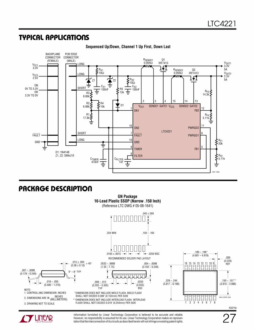
Sequenced Up/Down, Channel 1 Up First, Down Last
ON2
FAULT
GND
LTC4221
Z1 Z2
D11
16
7
10
9
8
FB2
PWRGD2
PWRGD1
VOUT13.3V5AVOUT22.5V5A
FB1
LONG
LONG
SHORT
GND
FAULTLONG
SHORT
D1: 1N4148Z1, Z2: SMAJ10
TIMER
FILTER
2 3 4 15 14 13
12
11
6
5
ON1
VCC1 SENSE1 GATE1 VCC2 SENSE2 GATE2
VCC13.3V
VCC22.5V
ON0V TO 3.3V
OR3.3V TO 0V
BACKPLANECONNECTOR
(FEMALE)
PCB EDGECONNECTOR
(MALE)
RX110Ω
RX210Ω
R513kR3
8.06k
R26.98k
R410k
R117.8k
RF314.3k
Q2IRF7413
RF45.11k
RF120k
RF25.11k
4221 TA05
CX1100nF
CFILTER1nF
CTIMER470nF
CX2100nF
Q1IRF7413
RSENSE10.004Ω
RSENSE20.004Ω
TYPICAL APPLICATIO S
U
Information furnished by Linear Technology Corporation is believed to be accurate and reliable.However, no responsibility is assumed for its use. Linear Technology Corporation makes no represen-tation that the interconnection of its circuits as described herein will not infringe on existing patent rights.

28
LTC4221
4221fa
© LINEAR TECHNOLOGY CORPORATION 2004
LT 0707 REV A • PRINTED IN THE USA
PART NUMBER DESCRIPTION COMMENTS
LTC1421 2-Channel, Hot Swap Controller 24-Pin, Operates from 3V to 12V and Supports –12V
LTC1422 Single Channel, Hot Swap Controller in SO-8 Operates from 2.7V to 12V, System Reset Output
LTC1642 Fault Protected, Hot Swap Controller Operates up to 16.5V, Overvoltage Protection to 33V
LTC1643AL/LTC1643AH PCI Hot Swap Controllers 3.3V, 5V and ±12V Supplies
LTC1645 Dual Channel Hot Swap Controller Operates from 1.2V to 12V, Power Sequencing
LTC1647 Dual Channel, Hot Swap Controller Operates from 2.7V to 16.5V
LTC4210 Single Channel, Hot Swap Controller in SOT-23 Operates from 2.7V to 16.5V, Multifunction Current Control
LTC4211 Single Channel, Hot Swap Controller in MSOP 2.5V to 16.5V, Multifunction Current Control
LTC4230 Triple Channel, Hot Swap Controller 1.7V to 16.5V, Multifunction Current Control
LTC4251 –48V Hot Swap Controller in S0T-23 –48V Hot Swap Controller, Active Current Limiting
LTC4252 –48V Hot Swap Controller in MSOP Active Current Limiting With Drain Acceleration
LTC4253 –48V Hot Swap Controller and Sequencer Active Current Limiting With Drain Acceleration and ThreeSequenced Power Good Outputs
RELATED PARTS
Linear Technology Corporation1630 McCarthy Blvd., Milpitas, CA 95035-7417(408) 432-1900 ● FAX: (408) 434-0507 ● www.linear-tech.com
TYPICAL APPLICATIO
U
Sequenced Up/Down, Channel 2 Up First, Down Last
ON2
FAULT
GND
LTC4221
Z1 Z2
D1
FB2
PWRGD2
PWRGD1
VOUT13.3V5AVOUT22.5V5A
FB1
LONG
LONG
SHORT
GND
FAULTLONG
SHORT
D1: 1N4148Z1, Z2: SMAJ10
TIMER
FILTER
ON1
VCC1 SENSE1 GATE1 VCC2 SENSE2 GATE2
VCC13.3V
VCC22.5V
ON0V TO 3.3V
OR3.3V TO 0V
BACKPLANECONNECTOR
(FEMALE)
PCB EDGECONNECTOR
(MALE)
RX110Ω
RX210Ω
R610k
R312.1k
R220.5k
R423.2k
R123.7k
R59.53k
RF314.3k
Q2IRF7413
RF45.11k
RF120k
RF25.11k
4221 TA06
CX1100nF
CFILTER1nF
CTIMER470nF
CX2100nF
Q1IRF7413
RSENSE10.004Ω
RSENSE20.004Ω