lan9370 5-port avb/tsn gigabit ethernet switch with
TRANSCRIPT
LAN93705-Port AVB/TSN Gigabit Ethernet Switch
with Integrated 100BASE-T1 PHYs
Highlights
• 4x 100BASE-T1 ports • 1x RGMII/RMII/MII port• Cascade mode for higher port count• Enhanced EMC performance• Full AVB Audio Video Bridging• Time Sensitive Networking Support• High Available Seamless Redundancy (HSR)• OPEN Alliance TC10 Sleep/Wakeup• Over-temperature and under-voltage detection• LinkMD®+ enhanced cable diagnostics• FlexPWR® technology power management• Small-footprint wettable 64-pin VQFN (8 x 8 mm)
• AEC-Q100 automotive product qualification
• Grade 2 Automotive temperature (-40°C to +105°C)
Target Applications
• Advanced Driver-Assistance Systems (ADAS)• Infotainment• Telematics & Smart Antennas• In-Vehicle Backbone• Gateways
Features
• Switch Management Capabilities- Compliant to OPEN TC11 switch requirements
- 1K MAC table
- IEEE 802.1Q VLAN support
- AVB and TSN hardware support:
-IEEE 802.1AS time synchronization
-IEEE 1588v2 PTP and clock synchronization
-IEEE 802.Qav traffic shaping
-IEEE 802.1Qbv (TSN) time-aware scheduler
-IEEE 802.1Qci (TSN) ingress filtering and policing
- 8 shapers per port, one for each queue
- Smart low-latency cut-through forwarding mode
- High Availability Seamless Redundancy (HSR)
- Deep Packet Inspection (DPI) using TCAM
-TCAM classification of Layers 2,3,4 and beyond
- SPI or in-band host processor access
- Wire speed - non-blocking
• 4x Integrated 100BASE-T1 Ethernet PHYs - Compliant with IEEE 802.3bw-2015- 100Mbps over single balanced twisted pair cable- Extended cable reach >15m- On-chip filtering & termination for balanced UTP cable
• 1x Configurable External MAC Port- Reduced Gigabit Media Independent Interface (RGMII)
- Reduced Media Independent Interface (RMII) with 50MHz reference clock input/output option
- Media Independent Interface (MII) in PHY/MAC mode
• IEEE 1588v2 PTP and Clock Synchronization- Transparent Clock (TC) with auto correction update
- Leader and Follower Ordinary Clock (OC) support
- End-to-end (E2E) or peer-to-peer (P2P)
- PTP multicast and unicast message support
- PTP message transport over IPv4/v6 and IEEE 802.3
- IEEE 1588v2 PTP packet filtering
- Time Aware Precision GPIO
• Advanced Diagnostics & Security- OPEN Alliance (TC1) advanced diagnostics compliant
- LinkMD®+ cable diagnostic capabilities
-Determines cable opens/shorts/length
-Signal Quality Indicator (SQI) with MSE, peak values, and peak/threshold interrupt
- Self-test packet generator/detector
-Single burst and continuous traffic stream support
-Automatic L2 and configurable L3 and L4 headers
- Loopback modes (per IEEE 802.3bw)
- Extended MIB performance counters
- Deep packet inspection support for every packet/port
- IEEE 802.1AR (802.1x) port and MAC authentication
- IEEE 802.1Qci per stream ingress filtering & policing
• EtherGREEN™ Energy Efficiency- Low-power 100BASE-T1 PHY technology- OPEN Alliance TC10 sleep/wakeup (partial network-
ing)- Non-TC10 link partner energy detect wake-up support- Ultra-Deep-Sleep power down
• Low RF Emissions- Integrated transmission filtering- xMII data and 125MHz clock include programmable
slew rate control- OPEN Alliance (TC6) RGMII EPL compliant- Exceeds OPEN Alliance Transceiver EMC
Test Specification
2019-2021 Microchip Technology Inc. DS00002819B-page 1
LAN9370
TO OUR VALUED CUSTOMERS
It is our intention to provide our valued customers with the best documentation possible to ensure successful use of your Microchipproducts. To this end, we will continue to improve our publications to better suit your needs. Our publications will be refined andenhanced as new volumes and updates are introduced.
If you have any questions or comments regarding this publication, please contact the Marketing Communications Department viaE-mail at [email protected]. We welcome your feedback.
Most Current DocumentationTo obtain the most up-to-date version of this documentation, please register at our Worldwide Web site at:
http://www.microchip.com
You can determine the version of a data sheet by examining its literature number found on the bottom outside corner of any page. The last character of the literature number is the version number, (e.g., DS30000000A is version A of document DS30000000).
ErrataAn errata sheet, describing minor operational differences from the data sheet and recommended workarounds, may exist for cur-rent devices. As device/documentation issues become known to us, we will publish an errata sheet. The errata will specify therevision of silicon and revision of document to which it applies.
To determine if an errata sheet exists for a particular device, please check with one of the following:• Microchip’s Worldwide Web site; http://www.microchip.com• Your local Microchip sales office (see last page)
When contacting a sales office, please specify which device, revision of silicon and data sheet (include -literature number) you areusing.
Customer Notification SystemRegister on our web site at www.microchip.com to receive the most current information on all of our products.
DS00002819B-page 2 2019-2021 Microchip Technology Inc.
2019-2021 Microchip Technology Inc. DS00002819B-page 3
LAN9370
Table of Contents
1.0 Preface ............................................................................................................................................................................................ 42.0 Introduction ..................................................................................................................................................................................... 83.0 Pin Descriptions and Configuration ............................................................................................................................................... 104.0 Package Information ..................................................................................................................................................................... 18Appendix A: Product Brief Revision History ........................................................................................................................................ 22The Microchip Web Site ...................................................................................................................................................................... 23Customer Change Notification Service ............................................................................................................................................... 23Customer Support ............................................................................................................................................................................... 23Product Identification System ............................................................................................................................................................. 24
LAN9370
1.0 PREFACE
1.1 General Terms
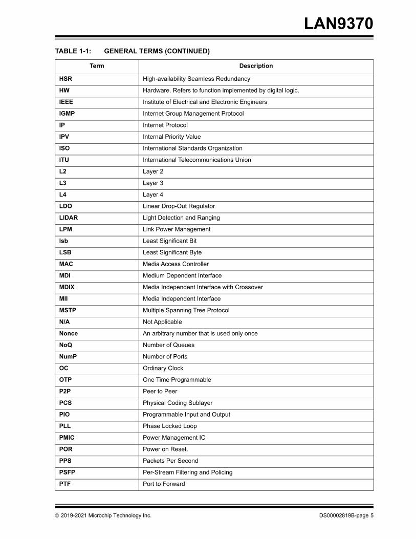
TABLE 1-1: GENERAL TERMS
Term Description
1000BASE-T 1 Gbps Ethernet over twisted pair, IEEE 802.3 compliant
100BASE-T1 100 Mbps Ethernet over single balanced twisted pair, IEEE 802.3bw compliant
100BASE-TX 100 Mbps Ethernet over twisted pair, IEEE 802.3 compliant
10BASE-T 10 Mbps Ethernet over twisted pair, IEEE 802.3 compliant
ACL Access Control List
ADAS Advanced Driver Assistance Systems
ADC Analog-to-Digital Converter
AFE Analog Front End
AN, ANEG Auto-Negotiation
ARP Address Resolution Protocol
AVB Audio Video Bridging
BELT Best Effort Latency Tolerance
BYTE 8-bits
CRC Cyclic Redundancy Check
CSMA/CD Carrier Sense Multiple Access/Collision Detect
CSR Control and Status Register
DA Destination Address
DoD Delay on Destination
DoS Delay on Source
DWORD 32-bits
E2E End to End
EC Embedded Controller
EEE Energy Efficient Ethernet
EOF End of Frame
FCS Frame Check Sequence
FID Filter ID
FIFO First In First Out buffer
FSM Finite State Machine
FW Firmware
GMII Gigabit Media Independent Interface
GPIO General Purpose I/O
gPTP Generic Precision Time Protocol
HOST External system (Includes processor, application software, etc.)
DS00002819B-page 4 2019-2021 Microchip Technology Inc.
LAN9370
HSR High-availability Seamless Redundancy
HW Hardware. Refers to function implemented by digital logic.
IEEE Institute of Electrical and Electronic Engineers
IGMP Internet Group Management Protocol
IP Internet Protocol
IPV Internal Priority Value
ISO International Standards Organization
ITU International Telecommunications Union
L2 Layer 2
L3 Layer 3
L4 Layer 4
LDO Linear Drop-Out Regulator
LIDAR Light Detection and Ranging
LPM Link Power Management
lsb Least Significant Bit
LSB Least Significant Byte
MAC Media Access Controller
MDI Medium Dependent Interface
MDIX Media Independent Interface with Crossover
MII Media Independent Interface
MSTP Multiple Spanning Tree Protocol
N/A Not Applicable
Nonce An arbitrary number that is used only once
NoQ Number of Queues
NumP Number of Ports
OC Ordinary Clock
OTP One Time Programmable
P2P Peer to Peer
PCS Physical Coding Sublayer
PIO Programmable Input and Output
PLL Phase Locked Loop
PMIC Power Management IC
POR Power on Reset.
PPS Packets Per Second
PSFP Per-Stream Filtering and Policing
PTF Port to Forward
TABLE 1-1: GENERAL TERMS (CONTINUED)
Term Description
2019-2021 Microchip Technology Inc. DS00002819B-page 5
LAN9370
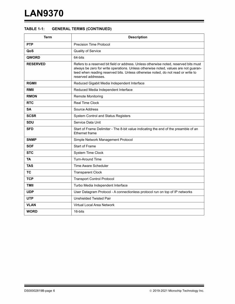
PTP Precision Time Protocol
QoS Quality of Service
QWORD 64-bits
RESERVED Refers to a reserved bit field or address. Unless otherwise noted, reserved bits must always be zero for write operations. Unless otherwise noted, values are not guaran-teed when reading reserved bits. Unless otherwise noted, do not read or write to reserved addresses.
RGMII Reduced Gigabit Media Independent Interface
RMII Reduced Media Independent Interface
RMON Remote Monitoring
RTC Real Time Clock
SA Source Address
SCSR System Control and Status Registers
SDU Service Data Unit
SFD Start of Frame Delimiter - The 8-bit value indicating the end of the preamble of an Ethernet frame
SNMP Simple Network Management Protocol
SOF Start of Frame
STC System Time Clock
TA Turn-Around Time
TAS Time Aware Scheduler
TC Transparent Clock
TCP Transport Control Protocol
TMII Turbo Media Independent Interface
UDP User Datagram Protocol - A connectionless protocol run on top of IP networks
UTP Unshielded Twisted Pair
VLAN Virtual Local Area Network
WORD 16-bits
TABLE 1-1: GENERAL TERMS (CONTINUED)
Term Description
DS00002819B-page 6 2019-2021 Microchip Technology Inc.
LAN9370
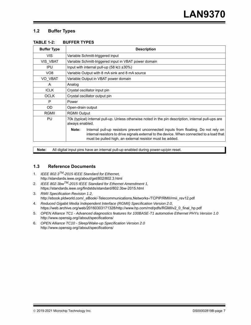
1.2 Buffer Types
1.3 Reference Documents
1. IEEE 802.3TM-2015 IEEE Standard for Ethernet, http://standards.ieee.org/about/get/802/802.3.html
2. IEEE 802.3bwTM-2015 IEEE Standard for Ethernet Amendment 1, https://standards.ieee.org/findstds/standard/802.3bw-2015.html
3. RMII Specification Revision 1.2,http://ebook.pldworld.com/_eBook/-Telecommunications,Networks-/TCPIP/RMII/rmii_rev12.pdf
4. Reduced Gigabit Media Independent Interface (RGMII) Specification Version 2.0,https://web.archive.org/web/20160303171328/http://www.hp.com/rnd/pdfs/RGMIIv2_0_final_hp.pdf
5. OPEN Alliance TC1 - Advanced diagnostics features for 100BASE-T1 automotive Ethernet PHYs Version 1.0http://www.opensig.org//about/specifications/
6. OPEN Alliance TC10 - Sleep/Wake-up Specification Version 2.0 http://www.opensig.org//about/specifications/
TABLE 1-2: BUFFER TYPES
Buffer Type Description
VIS Variable Schmitt-triggered input
VIS_VBAT Variable Schmitt-triggered input in VBAT power domain
IPU Input with internal pull-up (58 k ±30%)
VO8 Variable Output with 8 mA sink and 8 mA source
VO_VBAT Variable Output in VBAT power domain
A Analog
ICLK Crystal oscillator input pin
OCLK Crystal oscillator output pin
P Power
OD Open-drain output
RGMII RGMII Output
PU 70k (typical) internal pull-up. Unless otherwise noted in the pin description, internal pull-ups are always enabled.
Note: Internal pull-up resistors prevent unconnected inputs from floating. Do not rely oninternal resistors to drive signals external to the device. When connected to a load thatmust be pulled high, an external resistor must be added.
Note: All digital input pins have an internal pull-up enabled during power-up/pin reset.
2019-2021 Microchip Technology Inc. DS00002819B-page 7
LAN9370
2.0 INTRODUCTION
2.1 General Description
The Microchip LAN9370 is a scalable, compact and cost-effective, multi-Port AVB/TSN 100BASE-T1 Ethernet Switchbased on the IEEE 802.3bw-2015 specification. The LAN9370 incorporates a layer-2+ managed high-performanceEthernet switch, four 100BASE-T1 physical layer transceivers (PHYs), and one MAC port with a configurable RGMII/MII/RMII interface for direct connection to a host processor/controller, another Ethernet switch, or an Ethernet PHYtransceiver. The LAN9370 is available in a Grade 2 Automotive (-40°C to +105°C) temperature range and is qualifiedto AEC-Q100 automotive use cases such as gateways, Automated Driver-Assistance Systems (ADAS), infotainment,telematics and in-vehicle networking.
The LAN9370 fully supports the IEEE family of Audio Video Bridging (AVB) standards, which provide high Quality ofService (QoS) for latency sensitive traffic streams over Ethernet. Hardware time-stamping and time-keeping featuressupport IEEE 802.1AS (gPTP) and IEEE 1588v2 (PTP) time synchronization. All ports feature eight egress queues andan IEEE 802.1Qav credit based traffic shaper and time aware scheduler, as per the IEEE 802.1Qbv specification.
A host processor can access all LAN9370 registers for control over all PHY, MAC, and switch functions. Full registeraccess is available via the integrated SMI and SPI interfaces, and by in-band management via any one of the data ports.PHY register access is provided by a MIIM interface. Flexible digital I/O voltage allows the MAC port to interface directlywith a 1.8/2.5/3.3V host processor/controller/FPGA.
Additionally, a robust assortment of EtherGREENTM energy efficiency features are provided, including Open AllianceTC10 sleep/wakeup partial networking, non-TC10 link partner energy detect wake-up, and ultra-deep-sleep powerdown.
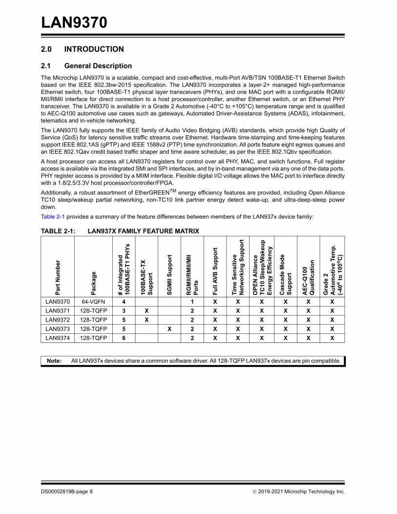
Table 2-1 provides a summary of the feature differences between members of the LAN937x device family:
TABLE 2-1: LAN937X FAMILY FEATURE MATRIX
Par
t N
um
ber
Pac
kag
e
# o
f In
teg
rate
d
100B
AS
E-T
1 P
HY
s
100B
AS
E-T
X
Su
pp
ort
SG
MII
Su
pp
ort
RG
MII/
RM
II/M
IIP
ort
s
Fu
ll A
VB
Su
pp
ort
Tim
e S
ensi
tiv
e N
etw
ork
ing
Su
pp
ort
OP
EN
Alli
ance
TC
10 S
leep
/Wak
eup
E
ner
gy
Eff
icie
ncy
Cas
cad
e M
od
eS
up
po
rt
AE
C-Q
100
Q
ual
ific
atio
n
Gra
de
2
Au
tom
oti
ve T
emp
.(-
40o
to
105
oC
)
LAN9370 64-VQFN 4 1 X X X X X X
LAN9371 128-TQFP 3 X 2 X X X X X X
LAN9372 128-TQFP 5 X 2 X X X X X X
LAN9373 128-TQFP 5 X 2 X X X X X X
LAN9374 128-TQFP 6 2 X X X X X X
Note: All LAN937x devices share a common software driver. All 128-TQFP LAN937x devices are pin compatible.
DS00002819B-page 8 2019-2021 Microchip Technology Inc.
LAN9370
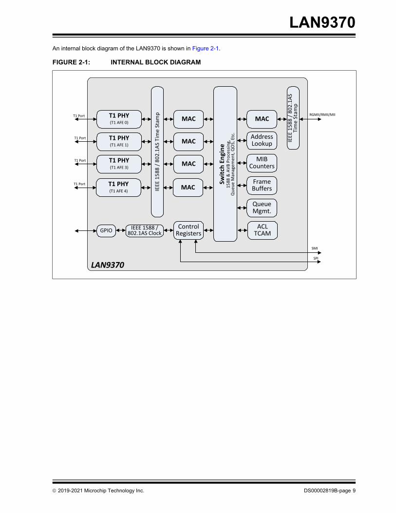
An internal block diagram of the LAN9370 is shown in Figure 2-1.
FIGURE 2-1: INTERNAL BLOCK DIAGRAM
LAN9370
T1 PHY(T1 AFE 0)
T1 PHY(T1 AFE 1)
T1 PHY(T1 AFE 3)
T1 Port
T1 Port
T1 Port
MAC
MAC
MAC
Switch Engine
1588 & AVB Processing,
Queue M
anagement, QOS, Etc.
ControlRegisters
MAC
AddressLookup
MIBCounters
FrameBuffers
QueueMgmt.
IEEE
1588 / 802.1AS Tim
e Stamp
IEEE 1588 / 802.1AS
Time Stamp
IEEE 1588 / 802.1AS ClockGPIO
T1 PHY(T1 AFE 4)
T1 PortMAC
RGMII/RMII/MII
SMI
SPI
ACLTCAM
2019-2021 Microchip Technology Inc. DS00002819B-page 9
LAN9370
3.0 PIN DESCRIPTIONS AND CONFIGURATION
3.1 Pin Assignments
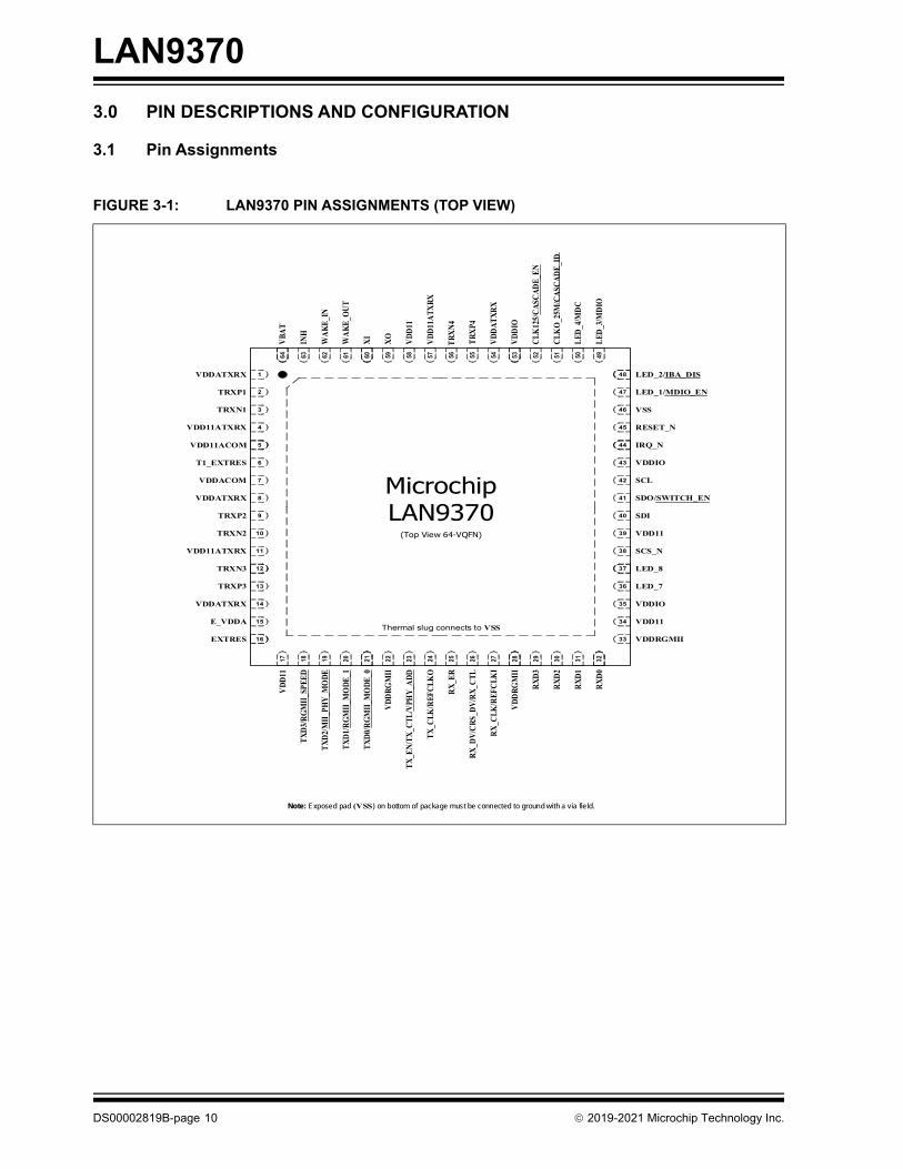
FIGURE 3-1: LAN9370 PIN ASSIGNMENTS (TOP VIEW)
MicrochipLAN9370
(Top View 64-VQFN)
Note: Exposed pad (VSS) on bottom of package must be connected to ground with a via field.
5
6
7
8
9
10
11
12
21 22 23 24 25 26 27 28
44
43
42
41
40
39
38
37
60 59 58 57 56 55 54 53
VDDATXRX
VDDACOM
TRXP2
TRXN2
VDD11ATXRX
TRXN3
TRXP3
VDDATXRX
VSS
RESET_N
VDDIO
SCS_N
LED_7
VDDIO
VD
D11
ATX
RX
TR
XN
4
CLK
O_2
5M/C
ASC
AD
E_ID
VD
D11
TR
XP4
VD
DR
GM
II
RX
_ER
VD
DR
GM
II
TX
D0/
RG
MII
_MO
DE
_0
TX
D1/
RG
MII
_MO
DE
_1
TX
D2/
MII
_PH
Y_M
OD
E
Thermal slug connects to VSS
CLK
125/
CA
SCA
DE_
EN
SCL
VD
DIO
RX
D3
VD
DA
TX
RX
TX
_CLK
/REF
CLK
O
IRQ_N
52 5162 61
3
4
13
14
19 20 29 30
36
35
46
45
TX
_EN
/TX
_CTL
/VPH
Y_A
DD
RX
_DV
/CR
S_D
V/R
X_C
TL
RX
_CLK
/REF
CLK
I
RX
D2
T1_EXTRES
VDD11ACOM
VDD11ATXRX
TRXN1
XO
XI
WA
KE
_OU
T
WA
KE
_IN
SDO/SWITCH_EN
SDI
VDD11
LED_8
1
2TRXP1
VDDATXRX
16
15
EXTRES
E_VDDA
17 18
VD
D11
TX
D3/
RG
MII
_SPE
ED
32R
XD
0
RX
D1
31
34
33 VDDRGMII
VDD11
48
LED_1/MDIO_EN47
LED_2/IBA_DIS
50 49
LED
_4/M
DC
LED
_3/M
DIO
64
INH
VBA
T
63
DS00002819B-page 10 2019-2021 Microchip Technology Inc.
LAN9370
TABLE 3-1: LAN9370 PIN ASSIGNMENTS
Pin Pin Name Pin Pin Name Pin Pin Name Pin Pin Name
1 VDDATXRX 17 VDD11 33 VDDRGMII 49 LED_3/MDIO
2 TRXP1 18 TXD3/RGMII_SPEED
34 VDD11 50 LED_4/MDC
3 TRXN1 19 TXD2/MII_PHY_MODE
35 VDDIO 51 CLKO_25M/CASCADE_ID
4 VDD11ATXRX 20 TXD1/RGMII_MODE_1
36 LED_7 52 CLK125/CASCADE_EN
5 VDD11ACOM 21 TXD0/RGMII_MODE_0
37 LED_8 53 VDDIO
6 T1_EXTRES 22 VDDRGMII 38 SCS_N 54 VDDATXRX
7 VDDACOM 23 TX_EN/TX_CTL/VPHY_ADD
39 VDD11 55 TRXP4
8 VDDATXRX 24 TX_CLK/REFCLKO 40 SDI 56 TRXN4
9 TRXP2 25 RX_ER 41 SDO/SWITCH_EN
57 VDD11ATXRX
10 TRXN2 26 RX_DV/CRS_DV/RX_CTL
42 SCL 58 VDD11
11 VDD11ATXRX 27 RX_CLK/REFCLKI 43 VDDIO 59 XO
12 TRXN3 28 VDDRGMII 44 IRQ_N 60 XI
13 TRXP3 29 RXD3 45 RESET_N 61 WAKE_OUT
14 VDDATXRX 30 RXD2 46 VSS 62 WAKE_IN
15 E_VDDA 31 RXD1 47 LED_1/MDIO_EN
63 INH
16 EXTRES 32 RXD0 48 LED_2/IBA_DIS
64 VBAT
Exposed Pad Must be Connected to VSS
2019-2021 Microchip Technology Inc. DS00002819B-page 11
LAN9370
3.2 Pin Descriptions
This section contains descriptions of the various LAN9370 pins. Buffer type definitions are detailed in Section 1.2, "Buf-fer Types".
The “_N” symbol in the signal name indicates that the active, or asserted, state occurs when the signal is at a low voltagelevel. For example, RESET_N indicates that the reset signal is active low. When “_N” is not present after the signalname, the signal is asserted when at the high voltage level.
Configuration straps allow various features of the device to be automatically configured to user defined values. Config-uration straps are identified by an underlined symbol name and are latched upon Power-On Reset (POR) and pin reset(RESET_N). Configuration straps include internal pull-up/pull-down resistors in order to prevent the signal from floatingwhen unconnected.
Note: Signals that function as configuration straps must be augmented with an external pull-up or pull-down resis-tor when connected to a load to ensure they reach the required voltage level prior to latching.
TABLE 3-2: PIN DESCRIPTIONS
Name SymbolBuffer Type
Description
100BASE-T1 Ethernet PHY Ports
Port 4-1 100BASE-T1PHY TX/RX
Positive
TRXP[4:1] A Port 4-1 100BASE-T1 PHY transmit/receive positive.
Port 4-1 100BASE-T1PHY TX/RX
Negative
TRXN[4:1] A Port 4-1 100BASE-T1 PHY transmit/receive negative.
100BASE-T1 Reference Resistor
T1_EXTRES A Reference resistor connection pin for the T1 PHY com-mon block. For proper operation, this pin must be con-nected to VSS through a 6.49kΩ 0.1% resistor.
Reference Resistor
EXTRES A Reference resistor connection pin. For proper operation, this pin must be connected to VSS through a 6.49kΩ +/-0.1% resistor.
RGMII/RMII/MII Port
RGMII/RMII/MII TransmitData 3
TXD3 RGMII MII/RGMII Modes: Transmit Data bus bit 3 output.
RMII Mode: Not used.
Note: This pin also provides configuration strap func-tions during hardware/software resets.
RGMII/RMII/MII TransmitData 2
TXD2 RGMII MII/RGMII Modes: Transmit Data bus bit 2 output.
RMII Mode: Not used.
Note: This pin also provides configuration strap func-tions during a hardware reset.
RGMII/RMII/MII TransmitData 1
TXD1 RGMII MII/RMII/RGMII Modes: Transmit Data bus bit 1 output.
Note: This pin also provides configuration strap func-tions during a hardware reset.
DS00002819B-page 12 2019-2021 Microchip Technology Inc.
LAN9370
RGMII/RMII/MII TransmitData 0
TXD0 RGMII MII/RMII/RGMII Modes: Transmit Data bus bit 0 output.
Note: This pin also provides configuration strap func-tions during a hardware reset.
RGMII/RMII/MII Transmit/Reference
Clock
TX_CLK/REFCLKO
RGMII MII Mode: TX_CLK is the 25/2.5MHz Transmit Clock. In PHY mode this pin is an output, in MAC mode it is an input.
RMII Mode: REFCLKO is the 50MHz Reference Clock output when in RMII Clock mode. This pin is unused when in RMII Normal mode.
RGMII Mode: TX_CLK is the 125/25/2.5MHz Transmit Clock output.
Note: This pin also provides configuration strap func-tions during a hardware reset.
RGMII/RMII/MII Transmit Enable/Control
TX_EN/TX_CTL
RGMII MII/RMII Modes: TX_EN is the Transmit Enable output.
RGMII Mode: TX_CTL is the Transmit Control output.
Note: This pin also provides configuration strap func-tions during a hardware reset.
RGMII/RMII/MII ReceiveData 3
RXD3 RGMII MII/RGMII Modes: Receive Data bus bit 3 input.
RMII Mode: Not used. Do not connect this pin in this mode of operation.
RGMII/RMII/MII ReceiveData 2
RXD2 RGMII MII/RGMII Modes: Receive Data bus bit 2 input.
RMII Mode: Not used. Do not connect this pin in this mode of operation.
RGMII/RMII/MII ReceiveData 1
RXD1 RGMII MII/RMII/RGMII Modes: Receive Data bus bit 1 input.
RGMII/RMII/MII ReceiveData 0
RXD0 RGMII MII/RMII/RGMII Modes: Receive Data bus bit 0 input.
RGMII/RMII/MII Receive Clock
RX_CLK/REFCLKI
RGMII MII Mode: RX_CLK is the 25/2.5MHz Receive Clock. In PHY mode this pin is an output, in MAC mode it is an input.
RMII Mode: REFCLKI is the 50MHz Reference Clock input when in RMII Normal mode. This pin is unused when in RMII Clock mode.
RGMII Mode: RX_CLK is the 125/25/2.5MHz Receive Clock output.
TABLE 3-2: PIN DESCRIPTIONS (CONTINUED)
Name SymbolBuffer Type
Description
2019-2021 Microchip Technology Inc. DS00002819B-page 13
LAN9370
RGMII/RMII/MII Receive
Data Valid / Carrier Sense
/ Control
RX_DV/CRS_DV/RX_CTL
RGMII MII Mode: RX_DV is the Receive Data Valid / Carrier Sense input.
RMII Mode: CRS_DV is the Carrier Sense / Receive Data Valid input.
RGMII Mode: RX_CTL is the Receive Control input.
RGMII/RMII/MII Receive Error
RX_ER RGMII MII/RMII Modes: Receive Error input.
RGMII Mode: Not used. Do not connect this pin in this mode of operation.
RGMII/RMII/MII 125 MHz
Reference Clock Output
CLK125 RGMII 125 MHz RGMII reference clock output to SoC MAC.
Note: This pin also provides configuration strap func-tions during a hardware reset.
SPI Pins
SPI Clock SCL VIS SPI clock.
The maximum supported SPI Clock frequency is 50 MHz.
SPIChip Select
SCS_N VIS Active-low SPI chip select input.
SPI Data Out SDO VO8 SPI output data.
Note: This pin also provides configuration strap func-tions during a hardware reset.
SPI Data In SDI VIS SPI input data.
MDIO Pins
SMI Data Input/Output
MDIO VIS/VO8 Serial Management Interface data input/output.
This pin is multiplexed with LED_3. The function of the pin is selected via the MDIO_EN configuration strap.
SMI Clock MDC VIS Serial Management Interface clock.
This pin is multiplexed with LED_4. The function of the pin is selected via the MDIO_EN configuration strap.
TABLE 3-2: PIN DESCRIPTIONS (CONTINUED)
Name SymbolBuffer Type
Description
DS00002819B-page 14 2019-2021 Microchip Technology Inc.
LAN9370
LED Pins
LED Indicator 1
LED_1 VIS/VO8 LED Indicator 1.
This pin may also function as a programmable input/out-put.
This signal can also be used as an input or output for use by the IEEE 1588 event trigger or time -stamp capture units. It will be synchronized to the internal IEEE 1588 clock.
Note: This pin also provides configuration strap func-tions during a hardware reset.
LED Indicator 2
LED_2 VIS/VO8 LED Indicator 2.
This pin may also function as a programmable input/out-put.
Note: This pin also provides configuration strap func-tions during a hardware reset.
LED Indicator 3
LED_3 VIS/VO8 LED Indicator 3.
This pin may also function as a programmable input/out-put.
LED Indicator 4
LED_4 VIS/VO8 LED Indicator 4.
This pin may also function as a programmable input/out-put.
LED Indicator 7
LED_7 VIS/VO8 LED Indicator 7.
This pin may also function as a programmable input/out-put.
LED Indicator 8
LED_8 VIS/VO8 LED Indicator 8.
This pin may also function as a programmable input/out-put.
Miscellaneous Pins
System Reset RESET_N VIS System reset. This pin is active low.
Note: When not used, this pin should be pulled-up toVDDIO.
Wake Input WAKE_IN VIS_VBAT Wakeup Input. Asserted to move the part out of sleep. This pin implements the optional wake input described in the OABR TC10 specification.
Note: This pin operates of off VBAT domain.
TABLE 3-2: PIN DESCRIPTIONS (CONTINUED)
Name SymbolBuffer Type
Description
2019-2021 Microchip Technology Inc. DS00002819B-page 15
LAN9370
Wake Output WAKE_OUT VO_VBAT Wake Output. Asserted when the part moves out of sleep. This pin implements the optional wake output described in the OABR TC10 specification.
Note: This pin operates of off VBAT domain.
Inhibit INH VO_VBAT Inhibit. Used to switch on/off the main external power sup-ply unit. This pin can be configured as an open source or open drain.
Note: When configured as open source, an externalpull-down is required. When configured asopen drain, this pin should be connected toVBAT via an external pull-up.
Note: RESET_N assertion does not affect the stateof this pin.
Interrupt IRQ_N VOD Active-low, open drain device interrupt.
Note: When unused, leave this pin unconnected.
25 MHz Reference
Clock
CLKO_25M/CASCADE_ID
VO8 25 MHz reference clock output.
Crystal Clock / Oscillator
Input
XI ICLK 25MHz Crystal clock / oscillator input. When using a crystal, this input is connected to one lead of the crystal. When using an oscillator, this pin is the input from the oscillator.
Crystal Clock Output
XO OCLK 25MHz Crystal clock output. When using a crystal, this output is connected to one lead of the crystal. When using an oscillator, this pin is left unconnected.
I/O Power pins, Core Power Pins, and Ground Pins
+1.8 - 3.3VI/O Power
Supply Input
VDDIO P +1.8 - 3.3V variable supply for IOs.
+1.1V Digital Core Power Supply Input
VDD11 P +1.1V digital core power.
+1.1V T1 Common
Block Power Supply
VDD11ACOM P +1.1V analog power supply for T1 common block.
+1.1V TX/RX
Analog Power Supply
VDD11ATXRX P +1.1V analog power supply for T1 PHY.
+2.5 - 3.3V TX/RX
Analog Power Supply
VDDATXRX P +2.5 - 3.3V analog power supply for T1 PHY.
TABLE 3-2: PIN DESCRIPTIONS (CONTINUED)
Name SymbolBuffer Type
Description
DS00002819B-page 16 2019-2021 Microchip Technology Inc.
LAN9370
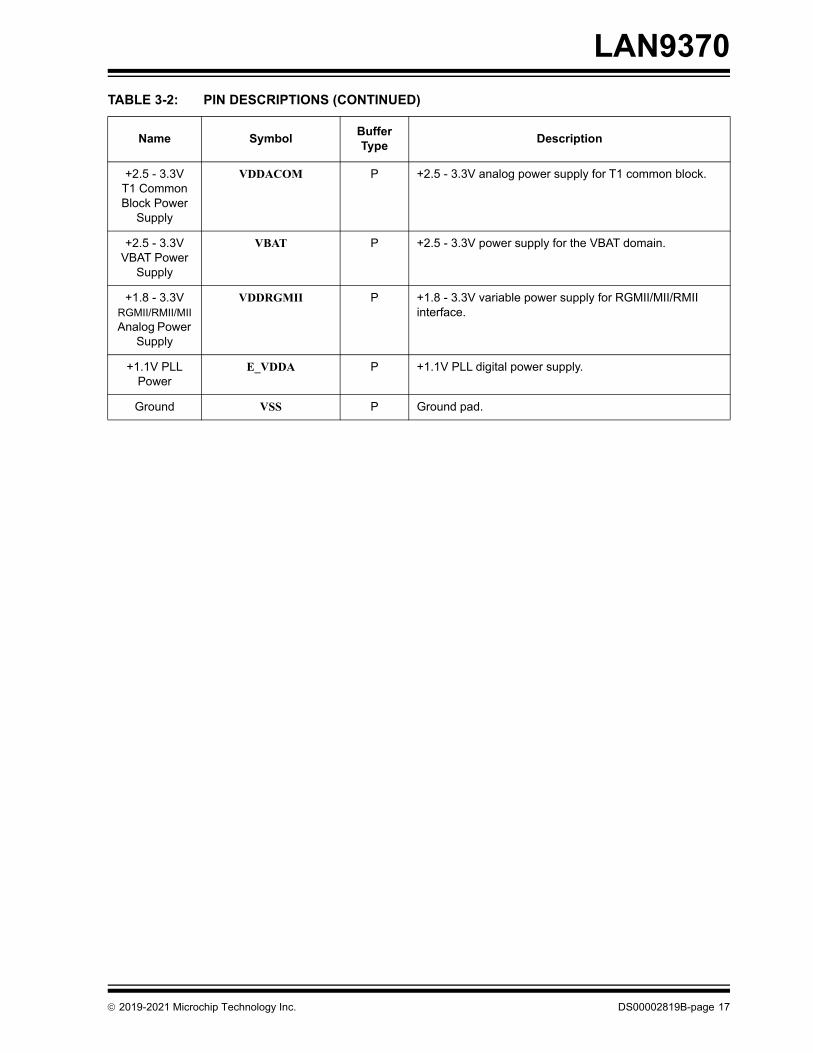
+2.5 - 3.3V T1 Common Block Power
Supply
VDDACOM P +2.5 - 3.3V analog power supply for T1 common block.
+2.5 - 3.3V VBAT Power
Supply
VBAT P +2.5 - 3.3V power supply for the VBAT domain.
+1.8 - 3.3V RGMII/RMII/MII Analog Power
Supply
VDDRGMII P +1.8 - 3.3V variable power supply for RGMII/MII/RMII interface.
+1.1V PLL Power
E_VDDA P +1.1V PLL digital power supply.
Ground VSS P Ground pad.
TABLE 3-2: PIN DESCRIPTIONS (CONTINUED)
Name SymbolBuffer Type
Description
2019-2021 Microchip Technology Inc. DS00002819B-page 17
LAN9370
4.0 PACKAGE INFORMATION
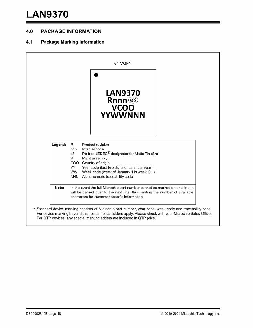
4.1 Package Marking Information
* Standard device marking consists of Microchip part number, year code, week code and traceability code.For device marking beyond this, certain price adders apply. Please check with your Microchip Sales Office.For QTP devices, any special marking adders are included in QTP price.
Legend: R Product revisionnnn Internal codee3 Pb-free JEDEC® designator for Matte Tin (Sn)V Plant assemblyCOO Country of originYY Year code (last two digits of calendar year)WW Week code (week of January 1 is week ‘01’)NNN Alphanumeric traceability code
Note: In the event the full Microchip part number cannot be marked on one line, itwill be carried over to the next line, thus limiting the number of availablecharacters for customer-specific information.
64-VQFN
LAN9370Rnnn e3VCOO
YYWWNNN
e3
DS00002819B-page 18 2019-2021 Microchip Technology Inc.
LAN9370
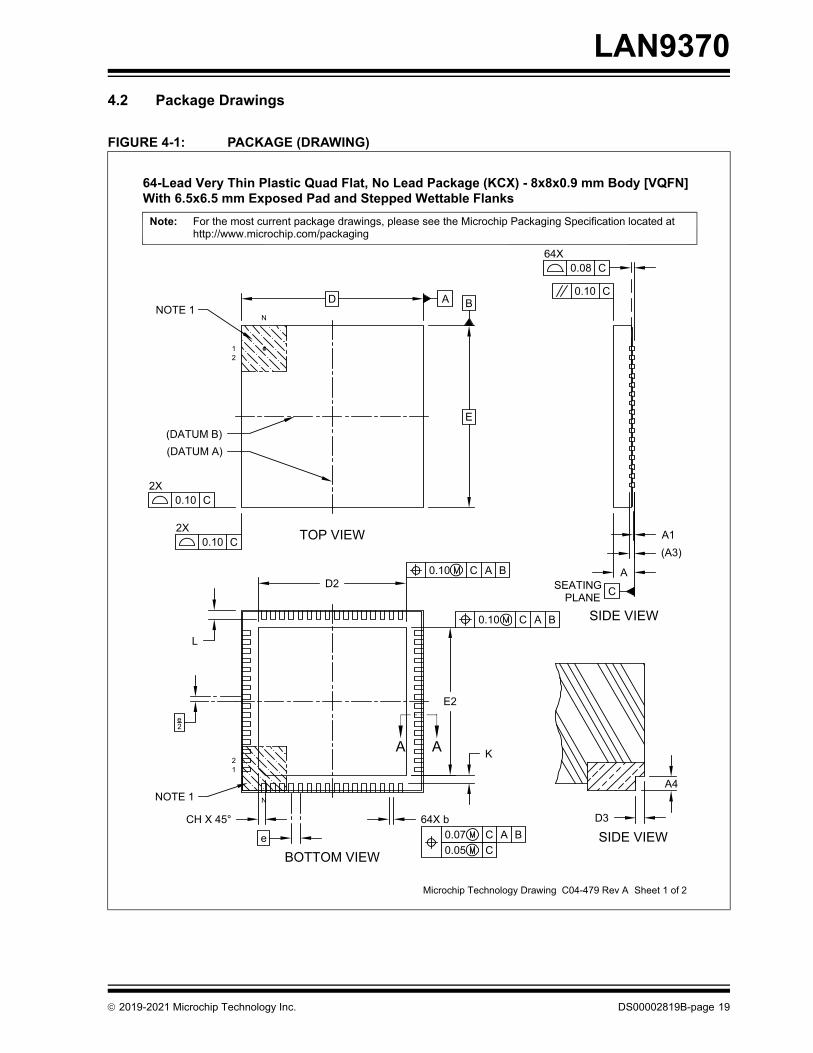
4.2 Package Drawings
FIGURE 4-1: PACKAGE (DRAWING)
BA
0.10 C
0.10 C
0.07 C A B0.05 C
(DATUM B)(DATUM A)
CSEATINGPLANE
NOTE 1
2X TOP VIEW
SIDE VIEW
BOTTOM VIEW
NOTE 1
12
N
0.10 C A B
0.10 C A B
0.10 C
0.08 C
Sheet 1 of 2
2X
64X
Note: For the most current package drawings, please see the Microchip Packaging Specification located athttp://www.microchip.com/packaging
64-Lead Very Thin Plastic Quad Flat, No Lead Package (KCX) - 8x8x0.9 mm Body [VQFN]With 6.5x6.5 mm Exposed Pad and Stepped Wettable Flanks
Microchip Technology Drawing C04-479 Rev A
SIDE VIEW
A1
A
(A3)
D
E
D2
E2
e
e2
64X b
KA A
12
N
L
A4
D3CH X 45°
2019-2021 Microchip Technology Inc. DS00002819B-page 19
LAN9370
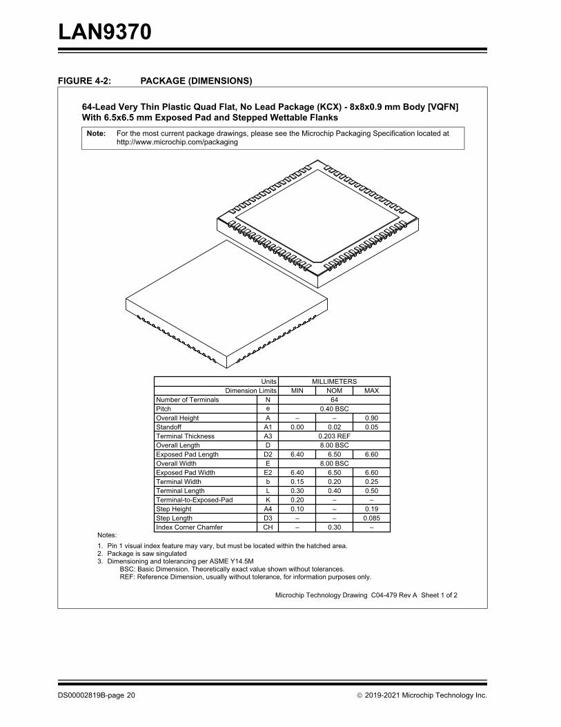
FIGURE 4-2: PACKAGE (DIMENSIONS)
For the most current package drawings, please see the Microchip Packaging Specification located athttp://www.microchip.com/packaging
Note:
REF: Reference Dimension, usually without tolerance, for information purposes only.BSC: Basic Dimension. Theoretically exact value shown without tolerances.
Notes:
1.2.3.
Pin 1 visual index feature may vary, but must be located within the hatched area.Package is saw singulatedDimensioning and tolerancing per ASME Y14.5M
Sheet 1 of 2
Number of Terminals
Overall Height
Terminal Width
Overall Width
Terminal Length
Exposed Pad Width
Terminal Thickness
Pitch
Standoff
UnitsDimension Limits
A1A
bE2
A3
e
L
E
N0.40 BSC
0.203 REF
0.300.15
–0.00
0.200.40
–0.02
8.00 BSC
MILLIMETERSMIN NOM
64
0.500.25
0.900.05
MAX
K –0.20 –Terminal-to-Exposed-Pad
Overall LengthExposed Pad Length
DD2 6.40
8.00 BSC6.50 6.60
Step Height A4D3
0.10 – 0.19–– 0.085Step Length
CH 0.30– –Index Corner Chamfer
6.40 6.50 6.60
64-Lead Very Thin Plastic Quad Flat, No Lead Package (KCX) - 8x8x0.9 mm Body [VQFN]With 6.5x6.5 mm Exposed Pad and Stepped Wettable Flanks
Microchip Technology Drawing C04-479 Rev A
DS00002819B-page 20 2019-2021 Microchip Technology Inc.
LAN9370
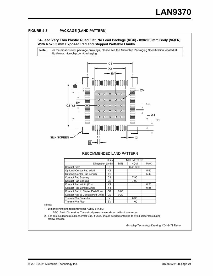
FIGURE 4-3: PACKAGE (LAND PATTERN)
RECOMMENDED LAND PATTERN
Dimension LimitsUnits
C2
Optional Center Pad Width
Contact Pad Spacing
Optional Center Pad Length
Contact Pitch
Y2X2
5.405.40
MILLIMETERS
0.40 BSCMIN
EMAX
7.90
Contact Pad Length (Xnn)Contact Pad Width (Xnn)
Y1X1
0.850.20
NOM
12
64
C1Contact Pad Spacing 7.90
Contact Pad to Contact Pad (Xnn) G2 0.20Thermal Via Diameter VThermal Via Pitch EV
0.301.00
BSC: Basic Dimension. Theoretically exact value shown without tolerances.
Notes:Dimensioning and tolerancing per ASME Y14.5M
For best soldering results, thermal vias, if used, should be filled or tented to avoid solder loss duringreflow process
1.
2.
For the most current package drawings, please see the Microchip Packaging Specification located athttp://www.microchip.com/packaging
Note:
Contact Pad to Center Pad (Xnn) G1 0.83
Microchip Technology Drawing C04-2479 Rev A
C1
C2EV
EV
X2
Y2
X1
Y1G1
G2
ØV
E
SILK SCREEN
64-Lead Very Thin Plastic Quad Flat, No Lead Package (KCX) - 8x8x0.9 mm Body [VQFN]With 6.5x6.5 mm Exposed Pad and Stepped Wettable Flanks
2019-2021 Microchip Technology Inc. DS00002819B-page 21
LAN9370
DS00002819B-page 22 2019-2021 Microchip Technology Inc.
APPENDIX A: PRODUCT BRIEF REVISION HISTORY
TABLE A-1: REVISION HISTORY
Revision Section/Figure/Entry Correction
DS0002819B (04-06-21) Public Release
DS00002819A (10-12-18) Initial Document Release
2019-2021 Microchip Technology Inc. DS00002819B-page 23
LAN9370
THE MICROCHIP WEB SITE
Microchip provides online support via our WWW site at www.microchip.com. This web site is used as a means to makefiles and information easily available to customers. Accessible by using your favorite Internet browser, the web site con-tains the following information:
• Product Support – Data sheets and errata, application notes and sample programs, design resources, user’s guides and hardware support documents, latest software releases and archived software
• General Technical Support – Frequently Asked Questions (FAQ), technical support requests, online discussion groups, Microchip consultant program member listing
• Business of Microchip – Product selector and ordering guides, latest Microchip press releases, listing of semi-nars and events, listings of Microchip sales offices, distributors and factory representatives
CUSTOMER CHANGE NOTIFICATION SERVICE
Microchip’s customer notification service helps keep customers current on Microchip products. Subscribers will receivee-mail notification whenever there are changes, updates, revisions or errata related to a specified product family ordevelopment tool of interest.
To register, access the Microchip web site at www.microchip.com. Under “Support”, click on “Customer Change Notifi-cation” and follow the registration instructions.
CUSTOMER SUPPORT
Users of Microchip products can receive assistance through several channels:
• Distributor or Representative
• Local Sales Office
• Field Application Engineer (FAE)
• Technical Support
Customers should contact their distributor, representative or field application engineer (FAE) for support. Local salesoffices are also available to help customers. A listing of sales offices and locations is included in the back of this docu-ment.
Technical support is available through the web site at: http://www.microchip.com/support
LAN9370
DS00002819B-page 24 2019-2021 Microchip Technology Inc.
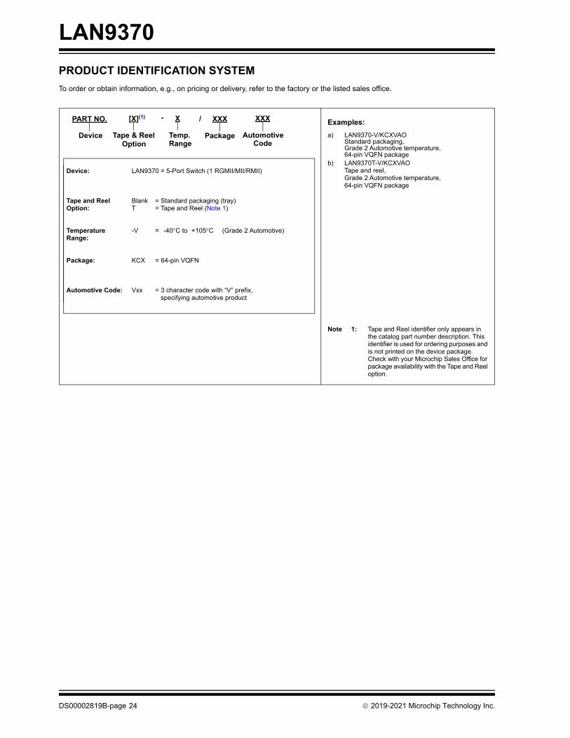
PRODUCT IDENTIFICATION SYSTEM
To order or obtain information, e.g., on pricing or delivery, refer to the factory or the listed sales office.
Device: LAN9370 = 5-Port Switch (1 RGMII/MII/RMII)
Tape and Reel Option:
Blank = Standard packaging (tray)T = Tape and Reel (Note 1)
Temperature Range:
-V = -40C to +105C (Grade 2 Automotive)
Package: KCX = 64-pin VQFN
Automotive Code: Vxx = 3 character code with “V” prefix, specifying automotive product
Examples:
a) LAN9370-V/KCXVAOStandard packaging, Grade 2 Automotive temperature,64-pin VQFN package
b) LAN9370T-V/KCXVAOTape and reel, Grade 2 Automotive temperature,64-pin VQFN package
Note 1: Tape and Reel identifier only appears in the catalog part number description. This identifier is used for ordering purposes and is not printed on the device package. Check with your Microchip Sales Office for package availability with the Tape and Reel option.
PART NO. X XXX
PackageTemp.Device
[X](1)
Tape & ReelOption Range
XXX
AutomotiveCode
- /
LAN9370Note the following details of the code protection feature on Microchip devices:
• Microchip products meet the specifications contained in their particular Microchip Data Sheet.
• Microchip believes that its family of products is secure when used in the intended manner and under normal conditions.
• There are dishonest and possibly illegal methods being used in attempts to breach the code protection features of the Microchip devices. We believe that these methods require using the Microchip products in a manner outside the operating specifications contained in Microchip's Data Sheets. Attempts to breach these code protection features, most likely, cannot be accomplished without violating Microchip's intellectual property rights.
• Microchip is willing to work with any customer who is concerned about the integrity of its code.
• Neither Microchip nor any other semiconductor manufacturer can guarantee the security of its code. Code protection does not mean that we are guaranteeing the product is "unbreakable." Code protection is constantly evolving. We at Microchip are committed to continuously improving the code protection features of our products. Attempts to break Microchip's code protection feature may be a violation of the Digital Millennium Copyright Act. If such acts allow unauthorized access to your software or other copyrighted work, you may have a right to sue for relief under that Act.
Information contained in this publication is provided for the sole purpose of designing with and using Microchip products. Information regarding device applications and the like is provided only for your convenience and may be superseded by updates. It is your responsi-bility to ensure that your application meets with your specifications.
THIS INFORMATION IS PROVIDED BY MICROCHIP "AS IS". MICROCHIP MAKES NO REPRESENTATIONS OR WARRANTIES OF ANY KIND WHETHER EXPRESS OR IMPLIED, WRITTEN OR ORAL, STATUTORY OR OTHERWISE, RELATED TO THE INFORMA-TION INCLUDING BUT NOT LIMITED TO ANY IMPLIED WARRANTIES OF NON-INFRINGEMENT, MERCHANTABILITY, AND FIT-NESS FOR A PARTICULAR PURPOSE OR WARRANTIES RELATED TO ITS CONDITION, QUALITY, OR PERFORMANCE.
IN NO EVENT WILL MICROCHIP BE LIABLE FOR ANY INDIRECT, SPECIAL, PUNITIVE, INCIDENTAL OR CONSEQUENTIAL LOSS, DAMAGE, COST OR EXPENSE OF ANY KIND WHATSOEVER RELATED TO THE INFORMATION OR ITS USE, HOWEVER CAUSED, EVEN IF MICROCHIP HAS BEEN ADVISED OF THE POSSIBILITY OR THE DAMAGES ARE FORESEEABLE. TO THE FULLEST EXTENT ALLOWED BY LAW, MICROCHIP'S TOTAL LIABILITY ON ALL CLAIMS IN ANY WAY RELATED TO THE INFOR-MATION OR ITS USE WILL NOT EXCEED THE AMOUNT OF FEES, IF ANY, THAT YOU HAVE PAID DIRECTLY TO MICROCHIP FOR THE INFORMATION. Use of Microchip devices in life support and/or safety applications is entirely at the buyer's risk, and the buyer agrees to defend, indemnify and hold harmless Microchip from any and all damages, claims, suits, or expenses resulting from such use. No licenses are conveyed, implicitly or otherwise, under any Microchip intellectual property rights unless otherwise stated.
Trademarks
The Microchip name and logo, the Microchip logo, Adaptec, AnyRate, AVR, AVR logo, AVR Freaks, BesTime, BitCloud, chipKIT, chipKIT logo, CryptoMemory, CryptoRF, dsPIC, FlashFlex, flexPWR, HELDO, IGLOO, JukeBlox, KeeLoq, Kleer, LANCheck, LinkMD, maXStylus, maXTouch, MediaLB, megaAVR, Microsemi, Microsemi logo, MOST, MOST logo, MPLAB, OptoLyzer, PackeTime, PIC, picoPower, PICSTART, PIC32 logo, PolarFire, Prochip Designer, QTouch, SAM-BA, SenGenuity, SpyNIC, SST, SST Logo, SuperFlash, Symmetricom, SyncServer, Tachyon, TimeSource, tinyAVR, UNI/O, Vectron, and XMEGA are registered trademarks of Microchip Technology Incorporated in the U.S.A. and other countries.AgileSwitch, APT, ClockWorks, The Embedded Control Solutions Company, EtherSynch, FlashTec, Hyper Speed Control, HyperLight Load, IntelliMOS, Libero, motorBench, mTouch, Powermite 3, Precision Edge, ProASIC, ProASIC Plus, ProASIC Plus logo, Quiet-Wire, SmartFusion, SyncWorld, Temux, TimeCesium, TimeHub, TimePictra, TimeProvider, WinPath, and ZL are registered trademarks of Microchip Technology Incorporated in the U.S.A.
Adjacent Key Suppression, AKS, Analog-for-the-Digital Age, Any Capacitor, AnyIn, AnyOut, Augmented Switching, BlueSky, BodyCom, CodeGuard, CryptoAuthentication, CryptoAutomotive, CryptoCompanion, CryptoController, dsPICDEM, dsPICDEM.net, Dynamic Average Matching, DAM, ECAN, Espresso T1S, EtherGREEN, IdealBridge, In-Circuit Serial Programming, ICSP, INICnet, Intelligent Paralleling, Inter-Chip Connectivity, JitterBlocker, maxCrypto, maxView, memBrain, Mindi, MiWi, MPASM, MPF, MPLAB Certified logo, MPLIB, MPLINK, MultiTRAK, NetDetach, Omniscient Code Generation, PICDEM, PICDEM.net, PICkit, PICtail, PowerSmart, PureSilicon, QMatrix, REAL ICE, Ripple Blocker, RTAX, RTG4, SAM-ICE, Serial Quad I/O, simpleMAP, SimpliPHY, SmartBuffer, SMART-I.S., storClad, SQI, SuperSwitcher, SuperSwitcher II, Switchtec, SynchroPHY, Total Endurance, TSHARC, USBCheck, VariSense, VectorBlox, VeriPHY, ViewSpan, WiperLock, XpressConnect, and ZENA are trademarks of Microchip Technology Incorporated in the U.S.A. and other countries.
SQTP is a service mark of Microchip Technology Incorporated in the U.S.A.The Adaptec logo, Frequency on Demand, Silicon Storage Technology, and Symmcom are registered trademarks of Microchip Technology Inc. in other countries.
GestIC is a registered trademark of Microchip Technology Germany II GmbH & Co. KG, a subsidiary of Microchip Technology Inc., in other countries.
All other trademarks mentioned herein are property of their respective companies.
© 2019-2021, Microchip Technology Incorporated, All Rights Reserved.
ISBN: 9781522478980
For information regarding Microchip’s Quality Management Systems, please visit www.microchip.com/quality.
2019-2021 Microchip Technology Inc. DS00002819B-page 25

2019-2021 Microchip Technology Inc. DS00002819B-page 26
AMERICASCorporate Office2355 West Chandler Blvd.Chandler, AZ 85224-6199Tel: 480-792-7200 Fax: 480-792-7277Technical Support: http://www.microchip.com/supportWeb Address: www.microchip.com
AtlantaDuluth, GA Tel: 678-957-9614 Fax: 678-957-1455
Austin, TXTel: 512-257-3370
BostonWestborough, MA Tel: 774-760-0087 Fax: 774-760-0088
ChicagoItasca, IL Tel: 630-285-0071 Fax: 630-285-0075
DallasAddison, TX Tel: 972-818-7423 Fax: 972-818-2924
DetroitNovi, MI Tel: 248-848-4000
Houston, TX Tel: 281-894-5983
IndianapolisNoblesville, IN Tel: 317-773-8323Fax: 317-773-5453Tel: 317-536-2380
Los AngelesMission Viejo, CA Tel: 949-462-9523Fax: 949-462-9608Tel: 951-273-7800
Raleigh, NC Tel: 919-844-7510
New York, NY Tel: 631-435-6000
San Jose, CA Tel: 408-735-9110Tel: 408-436-4270
Canada - TorontoTel: 905-695-1980 Fax: 905-695-2078
ASIA/PACIFICAustralia - SydneyTel: 61-2-9868-6733
China - BeijingTel: 86-10-8569-7000
China - ChengduTel: 86-28-8665-5511
China - ChongqingTel: 86-23-8980-9588
China - DongguanTel: 86-769-8702-9880
China - GuangzhouTel: 86-20-8755-8029
China - HangzhouTel: 86-571-8792-8115
China - Hong Kong SARTel: 852-2943-5100
China - NanjingTel: 86-25-8473-2460
China - QingdaoTel: 86-532-8502-7355
China - ShanghaiTel: 86-21-3326-8000
China - ShenyangTel: 86-24-2334-2829
China - ShenzhenTel: 86-755-8864-2200
China - SuzhouTel: 86-186-6233-1526
China - WuhanTel: 86-27-5980-5300
China - XianTel: 86-29-8833-7252
China - XiamenTel: 86-592-2388138
China - ZhuhaiTel: 86-756-3210040
ASIA/PACIFICIndia - BangaloreTel: 91-80-3090-4444
India - New DelhiTel: 91-11-4160-8631
India - PuneTel: 91-20-4121-0141
Japan - OsakaTel: 81-6-6152-7160
Japan - TokyoTel: 81-3-6880- 3770
Korea - DaeguTel: 82-53-744-4301
Korea - SeoulTel: 82-2-554-7200
Malaysia - Kuala LumpurTel: 60-3-7651-7906
Malaysia - PenangTel: 60-4-227-8870
Philippines - ManilaTel: 63-2-634-9065
SingaporeTel: 65-6334-8870
Taiwan - Hsin ChuTel: 886-3-577-8366
Taiwan - KaohsiungTel: 886-7-213-7830
Taiwan - TaipeiTel: 886-2-2508-8600
Thailand - BangkokTel: 66-2-694-1351
Vietnam - Ho Chi MinhTel: 84-28-5448-2100
EUROPEAustria - WelsTel: 43-7242-2244-39Fax: 43-7242-2244-393
Denmark - CopenhagenTel: 45-4485-5910 Fax: 45-4485-2829
Finland - EspooTel: 358-9-4520-820
France - ParisTel: 33-1-69-53-63-20 Fax: 33-1-69-30-90-79
Germany - GarchingTel: 49-8931-9700
Germany - HaanTel: 49-2129-3766400
Germany - HeilbronnTel: 49-7131-72400
Germany - KarlsruheTel: 49-721-625370
Germany - MunichTel: 49-89-627-144-0 Fax: 49-89-627-144-44
Germany - RosenheimTel: 49-8031-354-560
Israel - Ra’anana Tel: 972-9-744-7705
Italy - Milan Tel: 39-0331-742611 Fax: 39-0331-466781
Italy - PadovaTel: 39-049-7625286
Netherlands - DrunenTel: 31-416-690399 Fax: 31-416-690340
Norway - TrondheimTel: 47-7288-4388
Poland - WarsawTel: 48-22-3325737
Romania - BucharestTel: 40-21-407-87-50
Spain - MadridTel: 34-91-708-08-90Fax: 34-91-708-08-91
Sweden - GothenbergTel: 46-31-704-60-40
Sweden - StockholmTel: 46-8-5090-4654
UK - WokinghamTel: 44-118-921-5800Fax: 44-118-921-5820
Worldwide Sales and Service
02/28/20