l3 f10 2
TRANSCRIPT

EECS 247 Lecture 3: Filters © 2010 H.K. Page 1
EE247
Administrative
– Homework #1 will be posted on EE247 site
and is due Sept. 9th
– Office hours held @ 201 Cory Hall:
• Tues. and Thurs.: 4 to 5pm
EECS 247 Lecture 3: Filters © 2010 H.K. Page 2
EE247
Lecture 3• Active Filters
– Active biquads-
–How to build higher order filters?
• Integrator-based filters
– Signal flowgraph concept
– First order integrator-based filter
– Second order integrator-based filter & biquads
– High order & high Q filters
• Cascaded biquads & first order filters
– Cascaded biquad sensitivity to component mismatch
• Ladder type filters

EECS 247 Lecture 3: Filters © 2010 Page 3
Filters2nd Order Transfer Functions (Biquads)
• Biquadratic (2nd order) transfer function:
PQjH
jH
jH
P
)(
0)(
1)(0
2
2P P P
2 22
2P PP
P 2P
P
1P 2
1H( s )
s s1
Q
1H( j )
1Q
Biquad poles @: s 1 1 4Q2Q
Note: for Q poles are real , comple x otherwise
EECS 247 Lecture 3: Filters © 2010 Page 4
Biquad Complex Poles
Distance from origin in s-plane:
2
2
2
2 1412
P
P
P
P QQ
d
12
2
Complex conjugate poles:
s 1 4 12
P
PP
P
Q
j QQ
poles
j
d
S-plane

EECS 247 Lecture 3: Filters © 2010 Page 5
s-Plane
poles
j
P radius
P2Q- part real P
PQ2
1arccos
2s 1 4 12
PP
P
j QQ
EECS 247 Lecture 3: Filters © 2010 Page 6
Example
2nd Order Butterworthj
45 deg
2 2
4 2 2
Since 2nd order Butterworth:
ree
Cos pQ
PQ2
1arccos

EECS 247 Lecture 3: Filters © 2010 Page 7
Implementation of Biquads
• Passive RC: only real poles can’t implement complex conjugate poles
• Terminated LC
– Low power, since it is passive
– Only fundamental noise sources load and source resistance
– As previously analyzed, not feasible in the monolithic form for f <350MHz
• Active Biquads
– Many topologies can be found in filter textbooks!
– Widely used topologies:
• Single-opamp biquad: Sallen-Key
• Multi-opamp biquad: Tow-Thomas
• Integrator based biquads
EECS 247 Lecture 3: Filters © 2010 Page 8
Active Biquad
Sallen-Key Low-Pass Filter
• Single gain element
• Can be implemented both in discrete & monolithic form
• “Parasitic sensitive”
• Versions for LPF, HPF, BP, …
Advantage: Only one opamp used
Disadvantage: Sensitive to parasitic – all pole no finite zeros
outV
C1
inV
R2R1
C2
G
2
2
1 1 2 2
1 1 2 1 2 2
( )
1
1
1 1 1
P P P
P
PP
GH s
s s
Q
R C R C
QG
R C R C R C

EECS 247 Lecture 3: Filters © 2010 Page 9
Addition of Imaginary Axis Zeros
• Sharpen transition band
• Can “notch out” interference
– Band-reject filter
• High-pass filter (HPF)
Note: Always represent transfer functions as a product of a gain term,
poles, and zeros (pairs if complex). Then all coefficients have a
physical meaning, and readily identifiable units.
2
Z2
P P P
2P
Z
s1
H( s ) K
s s1
Q
H( j ) K
EECS 247 Lecture 3: Filters © 2010 Page 10
Imaginary Zeros
• Zeros substantially sharpen transition band
• At the expense of reduced stop-band attenuation at
high frequenciesPZ
P
P
ff
Q
kHzf
3
2
100
104
105
106
107
-50
-40
-30
-20
-10
0
10
Frequency [Hz]
Magnitude
[dB
]
With zerosNo zeros
Real Axis
Imag A
xis
-2 -1.5 -1 -0.5 0 0.5 1 1.5 2
x 106
-2
-1.5
-1
-0.5
0
0.5
1
1.5
2
x 106
Pole-Zero Map

EECS 247 Lecture 3: Filters © 2010 Page 11
Moving the Zeros
PZ
P
P
ff
Q
kHzf
2
100
104 105 106 107-50
-40
-30
-20
-10
0
10
20
Frequency [Hz]
Magnitude
[dB
]
Pole-Zero Map
Real AxisIm
ag A
xis
-6 -4 -2 0 2 4 6
-6
-4
-2
0
2
4
6
x105
x105
EECS 247 Lecture 3: Filters © 2010 Page 12
Tow-Thomas Active Biquad
Ref: P. E. Fleischer and J. Tow, “Design Formulas for biquad active filters using three
operational amplifiers,” Proc. IEEE, vol. 61, pp. 662-3, May 1973.
• Parasitic insensitive
• Multiple outputs

EECS 247 Lecture 3: Filters © 2010 Page 13
Frequency Response
01
2
1001020
01
3
01
2
01
2
22
01
2
0021122
1
1
asas
babasabb
akV
V
asas
bsbsb
V
V
asas
babsbabk
V
V
in
o
in
o
in
o
• Vo2 implements a general biquad section with arbitrary poles and zeros
• Vo1 and Vo3 realize the same poles but are limited to at most one finite zero
• Possible to use combination of 3 outputs
EECS 247 Lecture 3: Filters © 2010 Page 14
Component Values
8
72
173
2821
11
1
21732
80
6
82
74
81
6
8
11
1
21753
80
1
1
R
Rk
CRR
CRRk
CRa
CCRRR
Ra
R
Rb
RR
RR
R
R
CRb
CCRRR
Rb
827
2
86
20
01
5
11212
4
1021
3
20
12
11
1
111
11
1
RkR
b
RR
Cb
akR
CbbakR
CakkR
Ca
kR
CaR
821 and , ,,, given RCCkba iii
thatfollowsit
11
21732
8
CRQ
CCRRR
R
PP
P

EECS 247 Lecture 3: Filters © 2010 H.K. Page 15
Higher-Order Filters in the Integrated Form
• One way of building higher-order filters (n>2) is via cascade of 2nd
order biquads & 1st order , e.g. Sallen-Key,or Tow-Thomas, & RC
2nd order
Filter ……
Nx 2nd order sections Filter order: n=2N
1 2 N
Cascade of 1st and 2nd order filters:
Easy to implement
Highly sensitive to component mismatch -good for low Q filters only
For high Q applications good alternative: Integrator-based ladder filters
2nd order
Filter 1st or 2nd order
Filter
EECS 247 Lecture 3: Filters © 2010 H.K. Page 16
Integrator Based Filters
• Main building block for this category of filters
Integrator
• By using signal flowgraph techniques
Conventional RLC filter topologies can be
converted to integrator based type filters
• How to design integrator based filters?
– Introduction to signal flowgraph techniques
– 1st order integrator based filter
– 2nd order integrator based filter
– High order and high Q filters
EECS 247 Lecture 3: Filters © 2010 H.K. Page 17
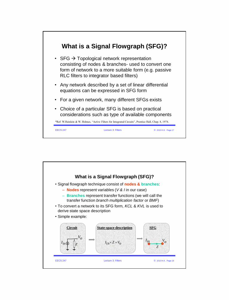
What is a Signal Flowgraph (SFG)?
• SFG Topological network representation
consisting of nodes & branches- used to convert one
form of network to a more suitable form (e.g. passive
RLC filters to integrator based filters)
• Any network described by a set of linear differential
equations can be expressed in SFG form
• For a given network, many different SFGs exists
• Choice of a particular SFG is based on practical
considerations such as type of available components
*Ref: W.Heinlein & W. Holmes, “Active Filters for Integrated Circuits”, Prentice Hall, Chap. 8, 1974.
EECS 247 Lecture 3: Filters © 2010 H.K. Page 18
What is a Signal Flowgraph (SFG)?
• Signal flowgraph technique consist of nodes & branches:
– Nodes represent variables (V & I in our case)
– Branches represent transfer functions (we will call the
transfer function branch multiplication factor or BMF)
• To convert a network to its SFG form, KCL & KVL is used to
derive state space description
• Simple example:
Circuit State-space description SFG
ZZ
VoinIinI
VoI Z Vin o

EECS 247 Lecture 3: Filters © 2010 H.K. Page 19
Signal Flowgraph (SFG)
Examples
1SL
Circuit State-space description SFG
R
L
R
oV
C 1SC
Vin
Vo
oI
VoinI
inI
inI
inI Vo
VinoI
I R Vin o
1V Iin o
SL
1I Vin o
SC
EECS 247 Lecture 3: Filters © 2010 H.K. Page 20
Useful Signal Flowgraph (SFG) Rules
1Va
2V
ba+b
1V2V
a.b1V
2V3Va b
1V 2V
a.V1+b.V1=V2 (a+b).V1=V2
a.V1=V3 (1)
b.V3=V2 (2)
Substituting for V3 from (1) in (2) (a.b).V1=V2
• Two parallel branches can be replaced by a single branch with overall BMF equal to
sum of two BMFs
• A node with only one incoming branch & one outgoing branch can be eliminated &
replaced by a single branch with BMF equal to the product of the two BMFs

EECS 247 Lecture 3: Filters © 2010 H.K. Page 21
Useful Signal Flowgraph (SFG) Rules
• An intermediate node can be multiplied by a factor (k). BMFs for incoming
branches have to be multiplied by k and outgoing branches divided by k
3V
a b1V 2V k.a b/k
1V 2V
3.Vk
a.V1=V3 (1)
b.V3=V2 (2)
Multiply both sides of (1) by k
(a.k) . V1= k.V3 (1)
Divide & multiply left side of (2) by k
(b/k) . k.V3 = V2 (2)
EECS 247 Lecture 3: Filters © 2010 H.K. Page 22
Useful Signal Flowgraph (SFG) Rules
hiV
2V a
oV
b
g-b
3V
hiV
2V a/(1+b)
oV
b
g
3V
3V
ciV
2V a
oV
b
d-bciV
2V a
oV-1 -b
1d
3V
• Simplifications can often be achieved by shifting or eliminating nodes
• Example: eliminating node V4
• A self-loop branch with BMF y can be eliminated by multiplying the BMF
of incoming branches by 1/(1-y)
V4

EECS 247 Lecture 3: Filters © 2010 H.K. Page 23
Integrator Based Filters1st Order LPF
• Conversion of simple lowpass RC filter to integrator-
based type by using signal flowgraph techniques
in
V 1o
s CV 1 R
oV
Rs
CinV
EECS 247 Lecture 3: Filters © 2010 H.K. Page 24
What is an Integrator?Example: Single-Ended Opamp-RC Integrator
oV
C
inV
-
+
R a
insC ,o o in o in
V 1 1V V V , V V dt
R sRC RC
• Node x: since opamp has high gain Vx=-Vo /a 0
• Node x is at “virtual ground”
No voltage swing at Vx combined with high opamp input impedance
No input opamp current
Vx
IR
IC

EECS 247 Lecture 3: Filters © 2010 H.K. Page 25
What is an Integrator?Example: Single-Ended Opamp-RC Integrator
inV -
Note: Practical integrator in CMOS technology has input & output both in the
form of voltage and not current Consideration for SFG derivation
oV
RC
oin
1VV sRC
01
RC
-90o
20log H
0dB
Phase
Ideal Magnitude &
phase response
EECS 247 Lecture 3: Filters © 2010 H.K. Page 26
1st Order LPF
Convert RC Prototype to Integrator Based Version
1. Start from circuit prototype-
Name voltages & currents for all components
2. Use KCL & KVL to derive state space description in such a way to have BMFs in the integrator form:
Capacitor voltage expressed as function of its current VCap.=f(ICap.)
Inductor current as a function of its voltage IInd.=f(VInd.)
3. Use state space description to draw signal flowgraph (SFG) (see next page)
1I
oV
Rs
CinV
2I
1V
CV

EECS 247 Lecture 3: Filters © 2010 H.K. Page 27
Integrator Based FiltersFirst Order LPF
1I
oV
1
Rs
CinV
2I
1V
1
Rs
1
sC
2I1I
CVinV 11 1V
• All voltages & currents nodes of SFG
• Voltage nodes on top, corresponding
current nodes below each voltage node
SFG
CV
oV1
V V V1 in C
1V IC 2
sC
V Vo C
1I V1 1 Rs
I I2 1
EECS 247 Lecture 3: Filters © 2010 H.K. Page 28
Normalize
• Since integrators are the main building blocks require in & out signals in the form of voltage (not current)
Convert all currents to voltages by multiplying current nodes by a scaling resistance R*
Corresponding BMFs should then be scaled accordingly
1 in o
11
2o
2 1
V V V
VI
Rs
IV
sC
I I
1 in o
**
1 1
*2
o *
* *2 1
V V V
RI R V
Rs
I RV
sC R
I R I R
* 'x xI R V
1 in o
*'
1 1
'2
o *
' '2 1
V V V
RV V
Rs
VV
sC R
V V

EECS 247 Lecture 3: Filters © 2010 H.K. Page 29
1st Order Lowpass Filter SGF
Normalize
'2V
*
1
sCR
oVinV 11 1V
1
*R
Rs
1
Rs
1
sC
2I1I
oVinV 11
1
1V
'1V
oVinV 11 1V
*R
Rs
1I R 2I R
*
1
sCR
*
*
R
R
EECS 247 Lecture 3: Filters © 2010 H.K. Page 30
1st Order Lowpass Filter SGF
Synthesis
'1V
1*
1
sC R
oVinV 11 1V
'2V1
*R
Rs
* *CR Rs , R
'1V
1
s
oVinV 11 1V
'2V1
1
s
oVinV 11 1V
'2V
1
Consolidate two branches
*
Choosing
R Rs

EECS 247 Lecture 3: Filters © 2010 H.K. Page 31
First Order Integrator Based Filter
oV
inV
-+
1
H ss
+
1
s
oVinV 11 1V
'2V
1
EECS 247 Lecture 3: Filters © 2010 H.K. Page 32
1st Order Filter
Built with Opamp-RC Integrator
oV
inV
-+
+
• Single-ended Opamp-RC integrator has a sign inversion from input to output
Convert SFG accordingly by modifying BMF
oV
inV
-
+-
oV
'in inV V
+
+-

EECS 247 Lecture 3: Filters © 2010 H.K. Page 33
1st Order Filter
Built with Opamp-RC Integrator
• To avoid requiring an additional opamp to perform summation at the input node:
oV
'in inV V
+
+-
oV
'inV
--
EECS 247 Lecture 3: Filters © 2010 H.K. Page 34
1st Order Filter
Built with Opamp-RC Integrator (continued)
o'
in
V 1
1 sRCV
oV
C
in'
V
-
+
R
R
--
oV'
inV

EECS 247 Lecture 3: Filters © 2010 H.K. Page 35
Opamp-RC 1st Order Filter
Noise
2n1v
k22
o mm0m 1
thi
2 21 2 2
2 2n1 n2
2o
v S ( f ) dfH ( f )
S ( f ) Noise spectral density of i noise sou rce
1H ( f ) H ( f )
1 2 fRC
v v 4KTR f
k Tv 2
C2
oV
C
-
+
R
R
Typically, increases as filter order increases
Identify noise sources (here it is resistors & opamp)
Find transfer function from each noise source
to the output (opamp noise next page)
2n2v
EECS 247 Lecture 3: Filters © 2010 H.K. Page 36
Opamp-RC Filter Noise
Opamp Contribution
2n1v
2opampv oV
C
-
+
R
R
• So far only the fundamental noise
sources are considered
• In reality, noise associated with the
opamp increases the overall noise
• For a well-designed filter opamp is
designed such that noise contribution
of opamp is negligible compared to
other noise sources
• The bandwidth of the opamp affects
the opamp noise contribution to the
total noise
2n2v

EECS 247 Lecture 3: Filters © 2010 H.K. Page 37
Integrator Based Filter
2nd Order RLC FilteroV
1
1
sL
R CinI•State space description:
R L C o
CC
RR
LL
C in R L
V V V V
IV
sC
VI
R
VI
sL
I I I I
• Draw signal flowgraph (SFG)
SFG
L
1
R
1
sC
CIRI
CV
inI
1
1
RV 1
1
LV
LI
CV
LI
+
-CI
LV
+
-
Integrator form
+
-
RV
RI
EECS 247 Lecture 3: Filters © 2010 H.K. Page 38
1 1
*R
R*
1
sCR
'1V
2V
inV
11
1V
*R
sL
1
oV
'3V
2nd Order RLC Filter SGF
Normalize
1
1
R
1
sC
CIRI
CV
inI
1
1
RV 1
1
LV
LI
1
sL
• Convert currents to voltages by multiplying all current nodes by the scaling
resistance R*
* 'x xI R V
'2V

EECS 247 Lecture 3: Filters © 2010 H.K. Page 39
inV
1*RR
2
1s1
1s
1 1
*R
R*
1
sCR
'1V
2V
inV
11
1V
*R
sL
1
oV
'3V
2nd Order RLC Filter SGF
Synthesis
oV
--
* *1 2R C L R
EECS 247 Lecture 3: Filters © 2010 H.K. Page 40
-20
-15
-10
-5
0
0.1 1 10
Second Order Integrator Based Filter
Normalized Frequency [Hz]
Mag
nit
ud
e (
dB
)
inV
1*RR
2
1s1
1s
BPV
-- LPV
HPV
Filter Magnitude Response

EECS 247 Lecture 3: Filters © 2010 H.K. Page 41
Second Order Integrator Based Filter
inV
1*RR
2
1s1
1s
BPV
-- LPV
HPV
BP 22in 1 2 2
LP2in 1 2 2
2HP 1 2
2in 1 2 2* *
1 2
*
0 1 2
1 2
1 2 *
V sV s s 1
V 1V s s 1
V sV s s 1
R C L R
R R
11
Q 1
From matching pointof v iew desirable :
RQR
L C
EECS 247 Lecture 3: Filters © 2010 H.K. Page 42
Second Order Bandpass Filter Noise
2 2n1 n2
2o
v v 4KTRdf
k Tv 2 Q
C
inV
1*RR
2
1s
1
1s
BPV
--
2n1v
2n2v
• Find transfer function of each noise
source to the output
• Integrate contribution of all noise
sources
• Here it is assumed that opamps are
noise free (not usually the case!)
k22
o mm0m 1
v S ( f ) dfH ( f )
Typically, increases as filter order increases
Note the noise power is directly proportion to Q
EECS 247 Lecture 3: Filters © 2010 H.K. Page 43
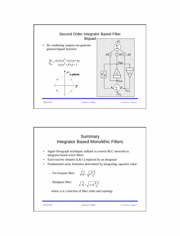
Second Order Integrator Based Filter
Biquad
inV
1*RR
2
1s1
1s
BPV
--
21 1 2 2 2 30
2in 1 2 2
a s a s aVV s s 1
oV
a1 a2 a3
HPV
LPV
• By combining outputs can generate
general biquad function:
s-planej
EECS 247 Lecture 3: Filters © 2010 H.K. Page 44
Summary
Integrator Based Monolithic Filters
• Signal flowgraph techniques utilized to convert RLC networks to
integrator based active filters
• Each reactive element (L& C) replaced by an integrator
• Fundamental noise limitation determined by integrating capacitor value:
– For lowpass filter:
– Bandpass filter:
where is a function of filter order and topology
2o
k Tv Q
C
2o
k Tv
C

EECS 247 Lecture 3: Filters © 2010 H.K. Page 45
Higher Order Filters
• How do we build higher order filters?
– Cascade of biquads and 1st order sections• Each complex conjugate pole built with a biquad and real pole
with 1st order section
• Easy to implement
• In the case of high order high Q filters highly sensitive to component mismatch
– Direct conversion of high order ladder type RLC filters• SFG techniques used to perform exact conversion of ladder type
filters to integrator based filters
• More complicated conversion process
• Much less sensitive to component mismatch compared to cascade of biquads
EECS 247 Lecture 3: Filters © 2010 H.K. Page 46
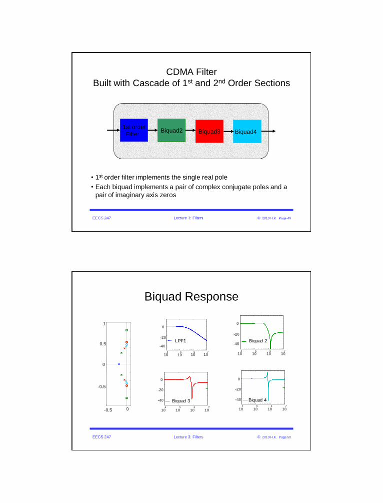
Higher Order FiltersCascade of Biquads
Example: LPF filter for CDMA cell phone baseband receiver
• LPF with
– fpass = 650 kHz Rpass = 0.2 dB
– fstop = 750 kHz Rstop = 45 dB
– Assumption: Can compensate for phase distortion in the digital domain
• Matlab used to find minimum order required 7th order Elliptic
Filter
• Implementation with cascaded BiquadsGoal: Maximize dynamic range
– Pair poles and zeros
– In the cascade chain place lowest Q poles first and progress to higher Q
poles moving towards the output node

EECS 247 Lecture 3: Filters © 2010 H.K. Page 47
Overall Filter Frequency Response
Bode DiagramP
hase (
deg)
Magnitude (
dB
)
-80
-60
-40
-20
0
-540
-360
-180
0
Frequency [Hz]
300kHz 1MHz
Mag
. (d
B)
-0.2
0
3MHz
EECS 247 Lecture 3: Filters © 2010 H.K. Page 48
Pole-Zero Map (pzmap in Matlab)
Qpole fpole [kHz]
16.7902 659.496
3.6590 611.744
1.1026 473.643
319.568
fzero [kHz]
1297.5
836.6
744.0
Pole-Zero Map
-2 -1.5 -1 -0.5 0-1
-0.5
0
0.5
1
Imag
Axis
X10
7
Real Axis x107
s-Plane
EECS 247 Lecture 3: Filters © 2010 H.K. Page 49
CDMA Filter
Built with Cascade of 1st and 2nd Order Sections
• 1st order filter implements the single real pole
• Each biquad implements a pair of complex conjugate poles and a
pair of imaginary axis zeros
1st order
Filter Biquad2 Biquad4 Biquad3
EECS 247 Lecture 3: Filters © 2010 H.K. Page 50
Biquad Response
104
105
106
107
-40
-20
0
LPF1
-0.5 0
-0.5
0
0.5
1
104
105
106
107
-40
-20
0
Biquad 2
104
105
106
107
-40
-20
0
Biquad 3
104
105
106
107
-40
-20
0
Biquad 4
EECS 247 Lecture 3: Filters © 2010 H.K. Page 51
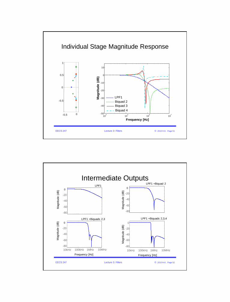
Individual Stage Magnitude Response
Frequency [Hz]
Mag
nit
ud
e (
dB
)
104
105
106
107
-50
-40
-30
-20
-10
0
10
LPF1
Biquad 2
Biquad 3
Biquad 4
-0.5 0
-0.5
0
0.5
1
EECS 247 Lecture 3: Filters © 2010 H.K. Page 52
Intermediate Outputs
Frequency [Hz]
Magnitude (
dB
)
-80
-60
-40
-20
Magnitude (
dB
)
LPF1 +Biquad 2
Magnitude (
dB
)
Biquads 1, 2, 3, & 4
Magnitude (
dB
)
-80
-60
-40
-20
0
LPF1
0
10kHz10
6
-80
-60
-40
-20
0
100kHz 1MHz 10MHz
5 6 7
-80
-60
-40
-20
0
4 5 6
Frequency [Hz]
10kHz10
100kHz 1MHz 10MHz
LPF1 +Biquads 2,3 LPF1 +Biquads 2,3,4

EECS 247 Lecture 3: Filters © 2010 H.K. Page 53
-10
Sensitivity to Relative Component Mismatch
Component variation in Biquad 4 relative to the rest
(highest Q poles):
– Increase p4 by 1%
– Decrease z4 by 1%
High Q poles High sensitivity
in Biquad realizationsFrequency [Hz]
1MHz
Magnitude (
dB
)
-30
-40
-20
0
200kHz
3dB
600kHz
-50
2.2dB
EECS 247 Lecture 3: Filters © 2010 H.K. Page 54
High Q & High Order Filters
• Cascade of biquads
– Highly sensitive to component mismatch not suitable
for implementation of high Q & high order filters
– Cascade of biquads only used in cases where required
Q for all biquads <4 (e.g. filters for disk drives)
• Ladder type filters more appropriate for high Q & high
order filters (next topic)
– Will show later Less sensitive to component mismatch

EECS 247 Lecture 3: Filters © 2010 H.K. Page 55
Ladder Type Filters
• Active ladder type filters
– For simplicity, will start with all pole ladder type filters
• Convert to integrator based form- example shown
– Then will attend to high order ladder type filters
incorporating zeros
• Implement the same 7th order elliptic filter in the form of
ladder RLC with zeros
– Find level of sensitivity to component mismatch
– Compare with cascade of biquads
• Convert to integrator based form utilizing SFG techniques
– Effect of integrator non-Idealities on filter frequency
characteristics
EECS 247 Lecture 3: Filters © 2010 H.K. Page 56
RLC Ladder Filters
Example: 5th Order Lowpass Filter
• Made of resistors, inductors, and capacitors
• Doubly terminated or singly terminated (with or w/o RL)
Rs
C1 C3
L2
C5
L4
inVRL
oV
Doubly terminated LC ladder filters Lowest sensitivity to
component mismatch

EECS 247 Lecture 3: Filters © 2010 H.K. Page 57
LC Ladder Filters
• First step in the design process is to find values for Ls and Cs based on specifications:
– Filter graphs & tables found in:
• A. Zverev, Handbook of filter synthesis, Wiley, 1967.
• A. B. Williams and F. J. Taylor, Electronic filter design, 3rd edition, McGraw-Hill, 1995.
– CAD tools
• Matlab
• Spice
Rs
C1 C3
L2
C5
L4
inVRL
oV
EECS 247 Lecture 3: Filters © 2010 H.K. Page 58
LC Ladder Filter Design Example
Design a LPF with maximally flat passband:
f-3dB = 10MHz, fstop = 20MHz
Rs >27dB @ fstop• Maximally flat passband Butterworth
From: Williams and Taylor, p. 2-37
Sto
pband A
ttenuatio
n
Normalized
• Find minimum filter order
:
• Here standard graphs
from filter books are
used
fstop / f-3dB = 2
Rs >27dB
Minimum Filter Order
c5th order Butterworth
1
-3dB
2
-30dB
Passband A
ttenuation

EECS 247 Lecture 3: Filters © 2010 H.K. Page 59
LC Ladder Filter Design Example
From: Williams and Taylor, p. 11.3
Find values for L & C from Table:
Note L &C values normalized to
-3dB =1
Denormalization:
Multiply all LNorm, CNorm by:
Lr = R/-3dB
Cr = 1/(RX-3dB )
R is the value of the source and
termination resistor
(choose both 1W for now)
Then: L= Lr xLNorm
C= Cr xCNorm
EECS 247 Lecture 3: Filters © 2010 H.K. Page 60
LC Ladder Filter Design Example
From: Williams and Taylor, p. 11.3
Find values for L & C from Table:
Normalized values:
C1Norm =C5Norm =0.618
C3Norm = 2.0
L2Norm = L4Norm =1.618
Denormalization:
Since -3dB =2x10MHz
Lr = R/-3dB = 15.9 nH
Cr = 1/(RX-3dB )= 15.9 nF
R =1
cC1=C5=9.836nF, C3=31.83nF
cL2=L4=25.75nH