k. n. toosi university of technology digital electronicswp.kntu.ac.ir/faradji/de/de_ch9-wm.pdf ·...
TRANSCRIPT

Digital Electronics Chapter 9. CMOS Logic
By: FARHAD FARADJI, Ph.D.
Assistant Professor, Electrical and Computer Engineering, K. N. Toosi University of Technology
http://wp.kntu.ac.ir/faradji/DigitalElectronics.htm
Reference:
DIGITAL INTEGRATED CIRCUITS: ANALYSIS and DESIGN, 2005, John E. Ayers
1
K. N. Toosi University of Technology
BByy:: FFAARRHHAADD FFAARAADDJJII, PPhh..DD..AAssssissttaanntt PPrrooffeesssoorr,,
EElleeccttrriiccaall aanndd CCoommppuutteerr EEnnggiinneeeerriinngg

9.1. Introduction Complementary metal oxide–semiconductor (CMOS) logic is by far most important logic family.
CMOS takes its name from fact that circuits use equal numbers of complementary n-channel and p-channel MOSFETs.
Popularity of CMOS has come about due to: – its extremely low standby power dissipation, – high packing density, and – high speed.
CMOS is used extensively in high-performance, portable (battery-operated) products such as: – notebook computers, – portable digital assistants, – pagers, and – wireless phones.
Chapter 9. CMOS Logic 2 Digital Electronics
KNTU
CMOS has come about due to:mely loww standby ppowwer ddiissssiippaatioon,
ingg ddeennssiittyy, aanndd ed.
eexxtteennssiivveellyy iinn hhiigghh-ppeerrffoorrmmaannccee, ppoorrttaabbllee ((

9.1. Introduction A CMOS inverter comprises 1 enhancement type n-MOSFET and 1 enhancement type p-MOSFET.
Normally-off devices are used for low standby dissipation.
With a logic-zero input (VIN = 0): – n-MOSFET is cut off. – p-MOSFET is linear. – Output goes high to VDD.
With a logic-one input (VIN = VDD): – n-MOSFET is linear. – p-MOSFET is cut off. – Output goes low to 0.
Supply current is small leakage current in a cutoff MOSFET.
DC dissipation is negligible.
CMOS is logic family of choice for battery-operated products.
Chapter 9. CMOS Logic 3 Digital Electronics
KNTU
T is cut off. T is lineear. oess hhiigghh ttoo VVDDDDVVV ..
onee iinnppuutt ((VVIINNVVVV = VVDDDDVV )):: TT iiss lliinneeaarr.

9.1. Introduction Packing density of CMOS is very high.
Because circuits use only MOSFETs.
MOSFETs in terms of chip area are: – 1/10 size of BJTs and – 1/500 size of resistors.
Only NMOS provides a higher packing density than CMOS.
NMOS requires only n-MOSFETs.
It is not necessary to fabricate p-type and n-type wells.
For most applications, slight packing density advantage of NMOS is overshadowed by superior DC dissipation of CMOS.
Chapter 9. CMOS Logic 4 Digital Electronics
KNTU
e of resistors.
providdeess aa hhigghherr ppaacckkinngg ddeennssiitty tthaann CCMMOOSS
es oonnlyy nn--MMOOSSFFEETTs.
ssssaarryy ttoo ffaabbrriiccaattee pp-ttyyppee aanndd nn-ttyyppee wweellllss..

9.2. Voltage Transfer Characteristic To determine VTC, 5 regimes of operation are considered.
9.2.1. n-MOSFET Cutoff, p-MOSFET Linear
VIN is less than VT of n-MOSFET.
Chapter 9. CMOS Logic 5 Digital Electronics
KNTU

9.2. Voltage Transfer Characteristic 9.2.2. n-MOSFET Saturated, p-MOSFET Linear
VIN is increased somewhat beyond VT of n-MOSFET.
VOUT is not known a priori.
Equation above should be used to calculate VOUT.
Above conditions should be checked to verify that results are meaningful.
Chapter 9. CMOS Logic 6 Digital Electronics
KNTU
VDSPO < 0 VDSPPOOV < 0
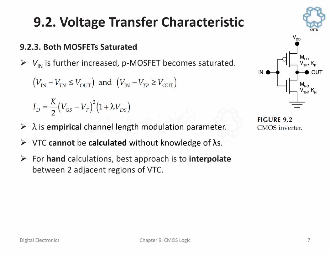
9.2. Voltage Transfer Characteristic 9.2.3. Both MOSFETs Saturated
VIN is further increased, p-MOSFET becomes saturated.
is empirical channel length modulation parameter.
VTC cannot be calculated without knowledge of s.
For hand calculations, best approach is to interpolate between 2 adjacent regions of VTC.
Chapter 9. CMOS Logic 7 Digital Electronics
KNTU
chhaannnneell lleennggtthh mmoodduulaatioonn ppaarraammeetteerr.. rrrr
e ccaallccuullaatteedd wwiitthhoouutt kknnoowwlleeddggee of s.

9.2. Voltage Transfer Characteristic 9.2.4. n-MOSFET Linear, p-MOSFET Saturated
Supply current is equal to ID in p-MOSFET (saturated).
VOUT is equal to VDS for n-MOSFET (linear).
Above conditions must be verified after calculation of VOUT.
Chapter 9. CMOS Logic 8 Digital Electronics
KNTU

9.2. Voltage Transfer Characteristic 9.2.5. n-MOSFET Linear, p-MOSFET Cutoff
VIN is sufficiently close to VDD.
Zero supply current flows.
Output goes to 0:
Logic swing of CMOS is equal to supply voltage.
This is called “rail-to-rail” operation.
CMOS has a rail-to-rail logic swing.
Chapter 9. CMOS Logic 9 Digital Electronics
KNTU
urrent fflows.
to 00::

9.2. Voltage Transfer Characteristic
Chapter 9. CMOS Logic 10 Digital Electronics
KNTU
VTC has an odd symmetry about midpoint where VIN = VOUT = VDD/2.

9.2. Voltage Transfer Characteristic Both transistors are saturated only at VIN = VDD/2. No interpolation is needed.
Chapter 9. CMOS Logic 11 Digital Electronics
KNTU

9.3. Propagation Delays For a symmetric CMOS inverter, 2 propagation delays are equal:
Chapter 9. CMOS Logic 12 Digital Electronics
KNTU

9.4. Fan-Out Fan-out of CMOS is determined entirely by dynamic considerations.
Suppose that a CMOS gate is loaded with similar CMOS circuits.
Only DC load current is due to leakage currents in MOS gates of switch transistors.
This current is negligible.
However, load gates present a significant capacitive load.
tP increases with fan-out.
Maximum fan-out is dictated by maximum tolerable tP.
Chapter 9. CMOS Logic 13 Digital Electronics
KNTU
s negligible.
d ggaatteess pprreesseenntt aa ssiiggnniffiiccaanntt ccaappaccittiivvee looaadd.
with fan-outt.
t ii ddii t t dd bb ii t ll bbll t

9.4. Fan-Out Consider a symmetric CMOS inverter loaded by N similar CMOS gate circuits.
Input capacitance for CMOS load gates is:
If maximum allowable tP is tP ,max, maximum allowable load capacitance is:
Maximum fan-out is largest integer satisfying:
Chapter 9. CMOS Logic 14 Digital Electronics
KNTU
alloowwaabbllee ttPP iiss ttPP ,,mmaaxx,, mmaaxxiimmuumm aalloowwaabblee llooaa

9.4. Fan-Out For low-frequency applications, maximum fan-out of a CMOS gate may be in hundreds or even thousands.
For higher-frequency applications, fan-out should be at least 10.
Smaller values greatly restrict logic design of system.
Chapter 9. CMOS Logic 15 Digital Electronics
KNTU
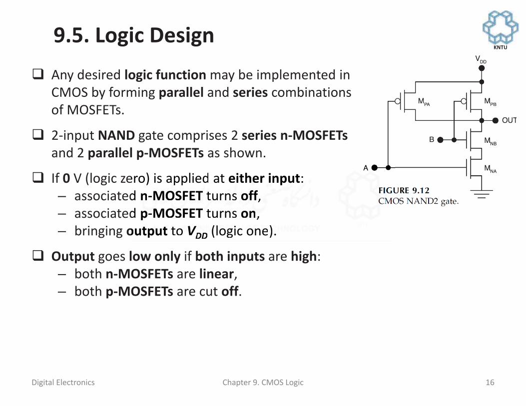
9.5. Logic Design Any desired logic function may be implemented in CMOS by forming parallel and series combinations of MOSFETs.
2-input NAND gate comprises 2 series n-MOSFETs and 2 parallel p-MOSFETs as shown.
If 0 V (logic zero) is applied at either input: – associated n-MOSFET turns off, – associated p-MOSFET turns on, – bringing output to VDD (logic one).
Output goes low only if both inputs are high: – both n-MOSFETs are linear, – both p-MOSFETs are cut off.
Chapter 9. CMOS Logic 16 Digital Electronics
KNTU
ero) is aappplied at eeiithheer innppuutt: d nn--MMOOSSFFEETT ttuurrnnss ooffff, d pp-MMOOSSFFEETT ttuurnnss onn, outtppuutt ttoo VVDDVV ((llooggiicc oonnee)).

9.5. Logic Design 3-input NAND gate comprises 3 series n-MOSFETs and 3 parallel p-MOSFETs as shown.
Output will go high if one or more of inputs go low.
Output is brought down to 0 V only if all 3 inputs are brought high.
M-input CMOS NAND gate requires M n-MOSFETs in series and M p-MOSFETs in parallel, for a total of 2M transistors.
Chapter 9. CMOS Logic 17 Digital Electronics
KNTU
ught doown to 0 VV oonllyy if aalll broouugghhtt hhiigghh..
OS NNAANNDD ggaattee rreeqquuiirreess MM nn-eerriieess aanndd MM pp-MMOOSSFFEETTss iinn

9.5. Logic Design 2-input CMOS NOR gate is implemented by placing 2 p-MOSFETs in series and 2 n-MOSFETs in parallel.
If logic 1 (VDD) is applied to either of inputs: – associated n-MOSFET turns on, – associated p-MOSFET turns off, – bringing output to 0 V.
Output goes high only if logic 0 is applied to both inputs.
In general, M-input CMOS NOR gate requires M n-MOSFETs and M p-MOSFETs (2M transistors).
Chapter 9. CMOS Logic 18 Digital Electronics
KNTU
output to 0 V.
higghh oonnllyy iiff llooggiicc 00 iiss aapppplliieedd ttoo bboothh
-iinnppuutt CCMMOOSS NNOORR ggaattee rreeqquuiirreess MM nn-

9.5. Logic Design Complex logic functions can be implemented in CMOS by combining parallel and series branches of n- and p-MOSFETs.
Chapter 9. CMOS Logic 19 Digital Electronics
KNTU

9.5. Logic Design In CMOS, XOR function is implemented using an AND–OR–INVERT approach.
Implementation of XOR2 in CMOS is inefficient.
It requires 12 MOSFETs.
5 MOSFETs needed in NMOS.
Chapter 9. CMOS Logic 20 Digital Electronics
KNTU
eeded in NMOS.

9.6. 4000 Series CMOS A corresponding range of tP has a fixed 50-pF load.
tP for CMOS varies inversely with supply voltage.
Longest tP of 330 ns corresponds to lowest supply voltage of 3 V.
Chapter 9. CMOS Logic 21 Digital Electronics
KNTU
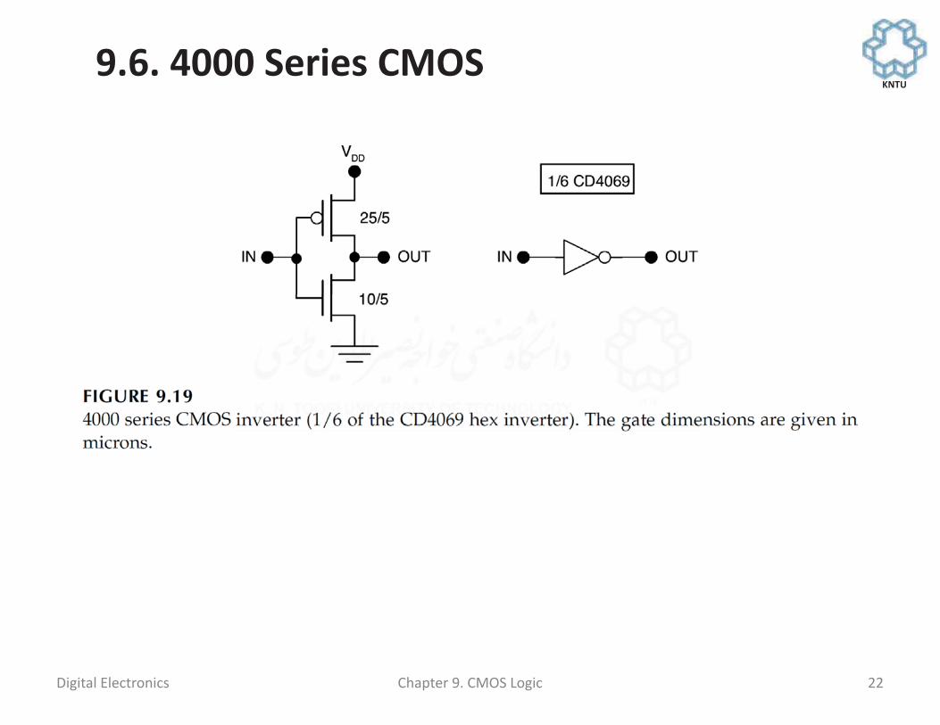
9.6. 4000 Series CMOS
Chapter 9. CMOS Logic 22 Digital Electronics
KNTU

9.6. 4000 Series CMOS
Chapter 9. CMOS Logic 23 Digital Electronics
KNTU

9.6. 4000 Series CMOS
Chapter 9. CMOS Logic 24 Digital Electronics
KNTU
9.7. 74HCxx Series CMOS
Chapter 9. CMOS Logic 25 Digital Electronics
KNTU
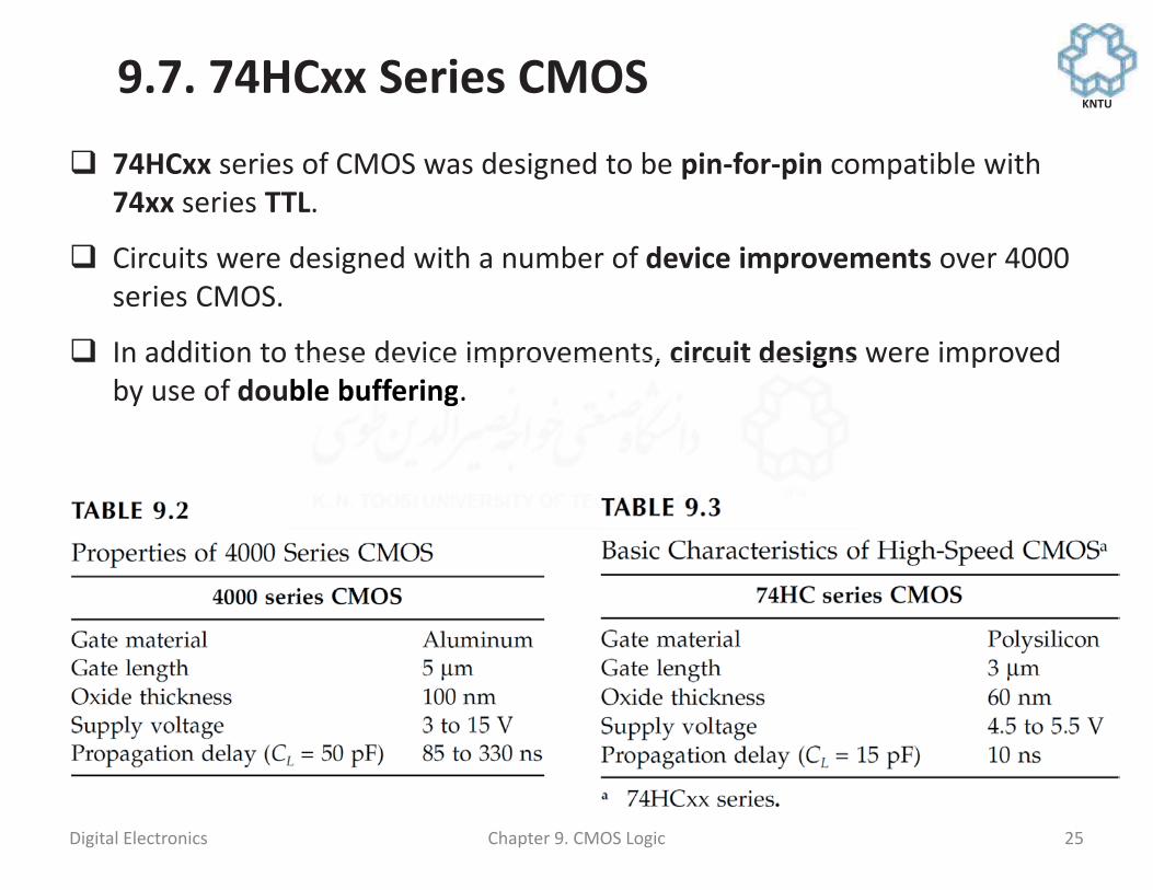
74HCxx series of CMOS was designed to be pin-for-pin compatible with 74xx series TTL.
Circuits were designed with a number of device improvements over 4000 series CMOS.
In addition to these device improvements, circuit designs were improved by use of double buffering.
these device improvements, circuit designsble buffferingg.

9.7. 74HCxx Series CMOS
Chapter 9. CMOS Logic 26 Digital Electronics
KNTU
74HC00 quad 2-input NAND gate comprises 4 identical circuits like one shown.
Circuit is double buffered by 2 inverters.
2 inverters do not alter overall logic function of circuit.
2 inverters provide voltage gain and current gain. ovide voltagee gaingain and and currentcurreent gaingaain.

9.7. 74HCxx Series CMOS
Chapter 9. CMOS Logic 27 Digital Electronics
KNTU
Double buffering improves VTC.
It does not exact a penalty in terms of dynamic performance

9.8. Buffered CMOS
Chapter 9. CMOS Logic 28 Digital Electronics
KNTU
A modern VLSI CMOS chip contains a million or more gates but only about 1000 external connections.
Most of gates experience only on-chip loads and are capable of tP in picoseconds without need for buffering.
For externally connected gates, significant capacitive loading exists.
Buffering is necessary to reduce tP and achieve acceptable off-chip data rates.
y connected gates, significant capacitive load
ecesssaarryy tto rreeduuccee ttPP aanndd aacchhiieevee aacccceepttaabble
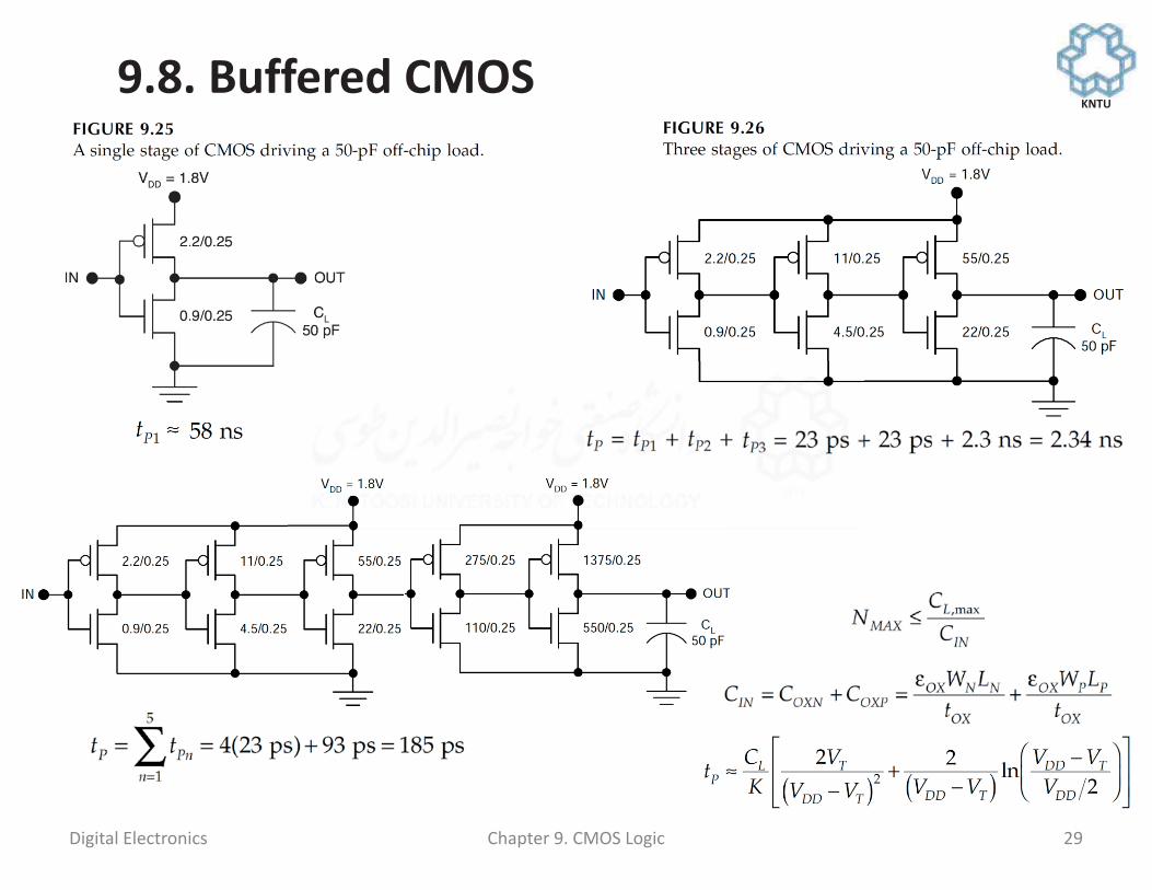
9.8. Buffered CMOS
Chapter 9. CMOS Logic 29 Digital Electronics
KNTU
9.8. Buffered CMOS
Chapter 9. CMOS Logic 30 Digital Electronics
KNTU
Buffering involves a trade-off between performance and chip area.
In 5-stage case, p-MOSFET of driving stage is so large that it could be seen by naked eye.
It has become common practice to use multiple buffering stages in modern CMOS gates.
Need for high off-chip data rates outweighs consideration of chip area.
S gates.
h off-cchhiipp ddattaa raatteess oouttwweeiigghhss connssiiddeeraattiioon

9.9. Pseudo NMOS
Chapter 9. CMOS Logic 31 Digital Electronics
KNTU
In CMOS technology it is possible to implement NMOS-type circuitry using a p-channel MOSFET load.
This type of logic circuitry is called “pseudo NMOS”.
A pseudo NMOS inverter is identical to an NMOS inverter with exception of load.
Load is an enhancement type p-channel MOSFET.
Circuit is compatible with CMOS fabrication technology, which does not provide for depletion type n-channel MOSFETS.
Gate of p-channel load is connected to ground rather than input, as in CMOS.
Pull-up is effectively passive.
erter with exception of load.
hancceemmeennt ttyypee pp-cchhannnneell MMOOSFFETT..
paattiibblee wwiitthh CCMMOOSS ffaabbricattiion tecchnnoollooggyy, ot pprroovviiddee ffoorr ddeepplleettiioonn ttyyppee nn--channeell MOS

9.9. Pseudo NMOS
Chapter 9. CMOS Logic 32 Digital Electronics
KNTU
Pseudo NMOS allows realization of arbitrary logic functions by addition of transistors to pull-down network.
X is a general input vector comprising any number of inputs.
Pseudo NMOS concept allows elimination of p-MOSFET pull-up network.
Pull-up network is replaced by a single p-channel MOSFET, regardless of complexity of logic function.
S concept allows elimination of ull-up neetwork.
orkk iiss rreeppllaacceedd bbyy aa ssiinnggle pp--cchhaannnneell arddlleessss ooff ccoommpplleexxiittyy ooff llooggiicc ffuunncctionn.

9.9. Pseudo NMOS
Chapter 9. CMOS Logic 33 Digital Electronics
KNTU
Generally, realization of a logic function involving N inputs requires: – N+1 transistors in pseudo NMOS but – 2N transistors in CMOS.
Disadvantage of pseudo NMOS is static power dissipation.
Under output low conditions, a steady DC current will flow in p-channel load and pull-down network.
e of pseudo NMOS is dissipattion.
t looww ccoonnddiittiioonnss, aa sstteeaaddy DDCC ccuurrrreenntt -chhaannnneell llooaadd aanndd ppuullll-ddoowwnn nneettwworkk.

9.9. Pseudo NMOS
Chapter 9. CMOS Logic 34 Digital Electronics
KNTU
Implementation of XOR2 function is rather efficient in pseudo NMOS.

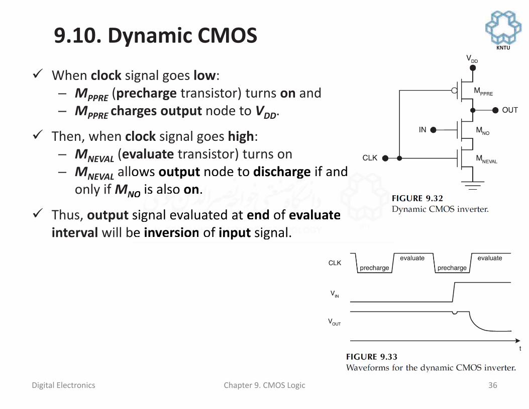
9.10. Dynamic CMOS
Chapter 9. CMOS Logic 35 Digital Electronics
KNTU
Dynamic, or clocked, CMOS gates achieve higher packing densities and lower dissipation than static CMOS gates discussed so far.
Principle underlying operation of dynamic CMOS is that CMOS circuit nodes exhibit capacitance and can be charged to a particular voltage level.
Once charged, such a node can be read at a later time as long as stored charge has not leaked away.
This principle is used in dynamic CMOS inverter.
d, such a node can be read at a later time as lot leakeed away.
iss uusseedd iinn ddyynnaammiicc CCMMOOSS iinnveerrtteer.
9.10. Dynamic CMOS
Chapter 9. CMOS Logic 36 Digital Electronics
KNTU
When clock signal goes low: – MPPRE (precharge transistor) turns on and – MPPRE charges output node to VDD.
Then, when clock signal goes high: – MNEVAL (evaluate transistor) turns on – MNEVAL allows output node to discharge if and
only if MNO is also on.
Thus, output signal evaluated at end of evaluate interval will be inversion of input signal.
ows output node to dischargge if aand NO is aallssoo oon.
siggnnal eevvaalluuaatteedd aat eenndd of evaluattebe iinnvveerrssiioonn ooff iinnppuutt ssiiggnnaall.

9.10. Dynamic CMOS
Chapter 9. CMOS Logic 37 Digital Electronics
KNTU
Output voltage dips slightly when input makes low-to-high transition (due to charge sharing).
Suppose output capacitor CY is initially precharged to VDD, but evaluation capacitance has 0 V on it.
If input makes a low-to-high transition: – MNO turns on. – Electrical charge initially present on CY is
shared between CY and CE:
s a low to high transition:s on. chhaarrggee iinniittiiaallllyy pprreesseenntt oonn CCYY iiss
etwweeen CCY aanndd CCEEC ::

9.10. Dynamic CMOS
Chapter 9. CMOS Logic 38 Digital Electronics
KNTU
Output voltage of a dynamic CMOS deteriorates very slowly with time.
This is because of low leakage currents associated with CMOS circuitry.
Eventually signal must be refreshed.
This necessitates that clock run at some minimum frequency in order to maintain signal integrity.
This is a disadvantage compared to static CMOS.
Static CMOS can be slowed down arbitrarily or even stopped.
Another disadvantage of dynamic CMOS is need for clock in first place.
nal must be refreshed.
ates tthhaatt ccllocckk ruunn aatt ssoommee mmiinnimmummorrddeerr ttoo mmaaiinnttaaiinn ssiiggnnaal inntteeggrriittyy.
dvaannttaaggee ccoommppaarreedd ttoo ssttaattiicc CCMMOS.
9.10. Dynamic CMOS
Chapter 9. CMOS Logic 39 Digital Electronics
KNTU
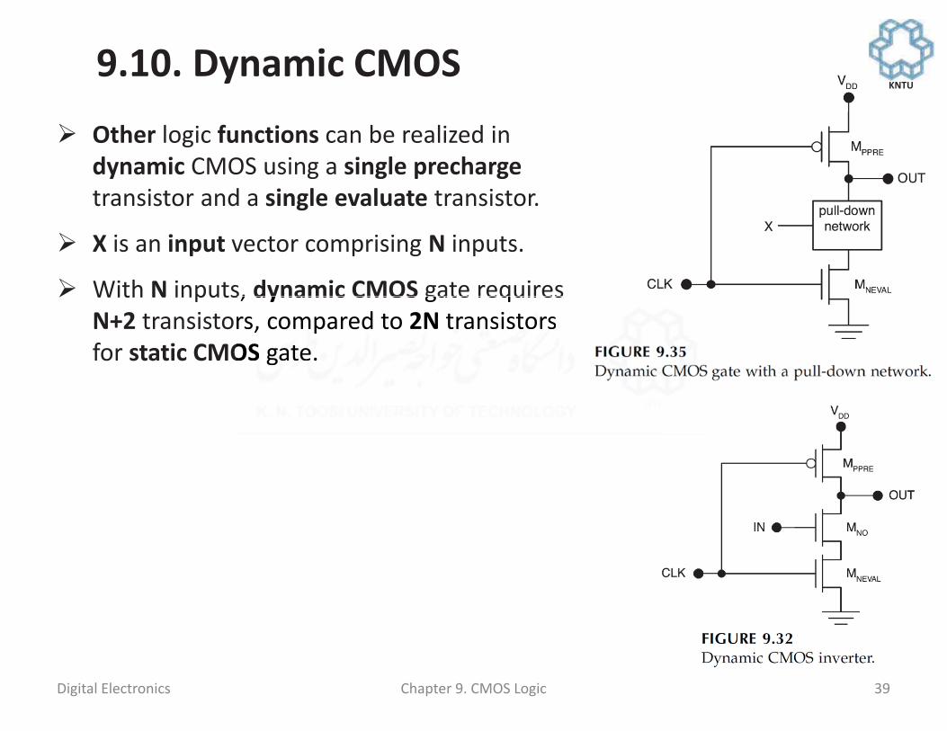
Other logic functions can be realized in dynamic CMOS using a single precharge transistor and a single evaluate transistor.
X is an input vector comprising N inputs.
With N inputs, dynamic CMOS gate requires N+2 transistors, compared to 2N transistors for static CMOS gate.
s, dynamic CMOS gate requires rs, commpared to 22NN ttrranssiisttoorrss OSS ggaattee.

9.10. Dynamic CMOS
Chapter 9. CMOS Logic 40 Digital Electronics
KNTU

9.10. Dynamic CMOS
Chapter 9. CMOS Logic 41 Digital Electronics
KNTU
An alternative form of dynamic CMOS uses a p-MOSFET pull-up network.
Pull-up or pull-down network may be eliminated, with a saving in chip area.
Either realization requires N+2 transistors for case of N inputs.
Pull-down realization is more efficient and usually preferred because of smaller width of n-MOSFETs compared with p-MOSFETs.
tion requires N 2 transistors inputs.
alizzaattiioonn iiss mmoorree eeffffiicciieenntreffeerrreedd bbeeccaauussee ooff ssmmaalllleerrOOSSFFEETTss ccoommppaarreedd wwiitthh pp-

9.10. Dynamic CMOS
Chapter 9. CMOS Logic 42 Digital Electronics
KNTU
Most serious limitation of dynamic CMOS in VLSI applications is that these circuits cannot be cascaded.
During first precharge interval of clock (clock low): – B and OUT nodes are precharged to
VDD.
During first evaluate interval (clock high): – MNOA is cut off, – B remains at VDD – OUT discharges when MNOB turns on. – OUT = A as required.
During next precharge interval: B remains at VDD OUT is charged up to VDD.
T nodes are prechargedd to
valluuatee iinntteerrvvaall (cclocckk hhigh)): ut ooffff,

9.10. Dynamic CMOS
Chapter 9. CMOS Logic 43 Digital Electronics
KNTU
Suppose that midway through this precharge interval, A input makes a transition from low to high.
This causes a dip in voltage at B due to charge sharing.
During next evaluate interval: – MNOA turns on, – B discharges to 0. – First cascaded inverter functions as
expected. – B does not discharge instantaneously. – During time that it takes for B to
discharge: • MNOB conducts. • OUT drops significantly below VDD.
valuatee interval:ns oonn,, geess tto 00. adeedd iinnvveerrtteerr ffuunnccttiioonnss aass

9.10. Dynamic CMOS
Chapter 9. CMOS Logic 44 Digital Electronics
KNTU
This results in a fake output signal that may not be interpreted as logic “one” by another gate.
In dynamic circuits, it is necessary that a circuit finish its evaluation phase before circuit in next stage starts its evaluation phase.
This can be achieved using a type of dynamic circuit referred to as “domino logic”.
in next stage uatioonn pphhaasee..
chiieevvedd uussinngg aa tyyppe ooff uit rreeffeerrrreedd ttoo aass

9.11. Domino Logic
Chapter 9. CMOS Logic 45 Digital Electronics
KNTU
In domino logic, circuits are designed so that a gate does not begin to evaluate until gates in previous stage have finished evaluating.
This is achieved by 2 modifications to dynamic CMOS: 1. Gates alternate between
use of pull-down and pull-up networks.
2. Gates with pull-up networks use an inverted clock signal.
ed by 2s to ddyynnaammicc
errnnaattee bbeettwweeeenn uullll--ddoowwnn aanndd ppuullll--