journal of materials chemistry c - ornlweb.ornl.gov/~geohegandb/lin jmc16 crsite3 nanosheets.pdf ·...
TRANSCRIPT
This journal is©The Royal Society of Chemistry 2016 J. Mater. Chem. C, 2016, 4, 315--322 | 315
Cite this: J.Mater. Chem. C, 2016,4, 315
Ultrathin nanosheets of CrSiTe3: a semiconductingtwo-dimensional ferromagnetic material†
Ming-Wei Lin,‡a Houlong L. Zhuang,‡a Jiaqiang Yan,bc Thomas Zac Ward,c
Alexander A. Puretzky,a Christopher M. Rouleau,a Zheng Gai,a Liangbo Liang,ad
Vincent Meunier,d Bobby G. Sumpter,ae Panchapakesan Ganesh,a Paul R. C. Kent,ae
David B. Geohegan,a David G. Mandrusbc and Kai Xiao*a
Finite range ferromagnetism and antiferromagnetism in two-dimensional (2D) systems within an isotropic
Heisenberg model at non-zero temperature were originally proposed to be impossible. However, recent
theoretical studies using an Ising model have shown that 2D magnetic crystals can exhibit magnetism.
Experimental verification of existing 2D magnetic crystals in this system has remained exploratory. In this
work we exfoliated CrSiTe3, a bulk ferromagnetic semiconductor, to mono- and few-layer 2D crystals
onto a Si/SiO2 substrate. Raman spectra indicate good stability and high quality of the exfoliated flakes,
consistent with the computed phonon spectra of 2D CrSiTe3, giving strong evidence for the existence of
2D CrSiTe3 crystals. When the thickness of the CrSiTe3 crystals is reduced to a few layers, we observed a
clear change in resistivity at 80–120 K, consistent with theoretical calculations of the Curie temperature
(Tc) of B80 K for the magnetic ordering of 2D CrSiTe3 crystals. The ferromagnetic mono- and few-layer
2D CrSiTe3 indicated here should enable numerous applications in nano-spintronics.
IntroductionThe emergence of novel properties and potential applications oftwo-dimensional (2D) crystals has recently stimulated consider-able worldwide attention.1–3 A particularly interesting class ofcandidate 2D crystals are the layered magnetic semiconductorswhich can simultaneously display semiconductor characteristicsand magnetic ordering that are advantageous for optoelectronicsand nano-spintronics applications.4–6 Both ferromagnetic (FM)and antiferromagnetic (AFM) layered semiconductors have been
characterized in bulk form, including their crystallographic andmagnetic structures.7–11 For example, chromium tellurosilicate(CrSiTe3) is a FM layered transition-metal chalcogenide (TMD)semiconductor, and exhibits ferromagnetic ordering at 32 K inthe bulk.7–8 Heisenberg type ferromagnetism has been foundbelow 6.25 K for K2CuF4 bulk crystals due to one percent ofthe anisotropic interlayer exchange interaction.11 Unlike othernon-magnetic 2D layered materials that require edge,12,13 strainengineering,14,15 a balanced hole-electron ‘‘resonance’’ condi-tion,16 or so called phase incorporation due to vacancies17 toachieve magnetic properties, the magnetic ordering in these 2Dsystems, such as CrSiTe3 or K2CuF4, could inherit magneticproperties from their parent layered 3D system. However, theexistence of 2D magnetic ordering is unclear, particularlywhether this is inherited from the parent 3D system. In anearlier report, calculations by Mermin and Wagner predictedthat spontaneous ferromagnetism and anti-ferromagnetismshould not exist based on a 2D isotropic Heisenberg model withlong-range order at non-zero temperature.18 Bruno also provedthe absence of spontaneous magnetic ordering in one- or two-dimensional Heisenberg systems with long-range interactions atfinite temperatures.19 Recently, the possibility of 2D K2CuF4 crystalsforming free-standing 2D flakes by exfoliation with a robust mag-netic moment of a Kosterlitz–Thouless type system was predictedfrom a first-principles theoretical analysis.5 Experimentally, a 2DMn stearate (MnSt2) magnet has been demonstrated by deposi-tion on a Si substrate using Langmuir–Blodgett technique.20
a Center for Nanophase Materials Sciences, Oak Ridge National Laboratory,Oak Ridge, TN 37831, USA. E-mail: [email protected]
b Department of Materials Science and Engineering, University of Tennessee,Knoxville, TN 37996, USA
c Materials Science and Technology Division, Oak Ridge National Laboratory,Oak Ridge, TN 37831, USA
d Department of Physics, Applied Physics, and Astronomy, Rensselaer PolytechnicInstitute, Troy, New York 12180, USA
e Computer Science and Mathematics Division, Oak Ridge National Laboratory,Oak Ridge, TN 37831, USA
† Electronic supplementary information (ESI) available: Results of theoreticalcalculations using various Ueff ranging from 0 to 10 eV are given in the Fig. S1.Detail information of Raman calculations for both monolayer and bulk is shownin the Fig. S2. Resistivity versus temperature measurements for the thickness of8.5 nm, 20 nm, 36 nm and 125 nm are demonstrated in the Fig. S3. Fig. S4illustrates the energies computed from different AFM spin textures, with p-typedoping consideration. See DOI: 10.1039/c5tc03463a‡ These authors contributed equally to this work.
Received 22nd October 2015,Accepted 25th November 2015
DOI: 10.1039/c5tc03463a
www.rsc.org/MaterialsC
Journal ofMaterials Chemistry C
PAPER

316 | J. Mater. Chem. C, 2016, 4, 315--322 This journal is©The Royal Society of Chemistry 2016
Moreover, a magnetic phase transition exhibiting a thicknessdependence due to a dramatic critical exponent b changehas been reported for Ni thin film,21,22 indicating changes inmagnetic ordering for a 2D Ising system at non-zero temperature.Recent studies associated with TMDs (TiCoO, CoSe and ZnO)nanosheets using chemical solution approaches also showed thesemiconductor characteristics with magnetism,23–26 demonstrat-ing the existence of magnetism for 2D nanosheets at non-zerotemperatures. To resolve the debate on the presence and origin ofmagnetism in these systems, layered 2D semiconductors, such asCrSiTe3, can be exfoliated layer-by-layer from a bulk crystal andcan be used as excellent testbeds.
CrSiTe3 is an indirect layered semiconductor with indirectand direct band gaps at 0.4 eV and 1.2 eV, respectively.8 Asshown in Fig. 1, CrSiTe3 is a layered material formed fromstacks of Te–(Cr, Si)–Te sandwich layers. One layer is composedof a Si2Te6 with two Cr ions inserted between two layers of Teplanes, leading to a van der Waals gap.27 Bulk CrSiTe3 exhibitsa quasi-2D Ising ferromagnetic behavior at Tc = 33 K28,29
Our previous report shows the strong coupling betweenthe magnetic and lattice degrees of freedom by the phononmeasurements across the 33 K ferromagnetic transition.8 TheSi–Te stretching and Te displacement modes are sensitive to themagnetic ordering transition,8 which indicates the magneticordering transition could be modified by a phonon dimension-ality crossover in 2D systems due to the quantum confinementof phonons. Recently, based on a Heisenberg model, it waspredicted that 2D ferromagnetic CrSiTe3 was dynamically stableand that the Curie temperature (Tc) would be dramaticallyshifted to higher temperature in single layer compared to thebulk.30,31 In some published results, they also showed theexistence of uniaxial easy axis for monolayer CrSiTe3 crystalbased on 2D Ising model, which was more suitable to predict theTc change.6,32 However, other theoretical calculations predictedthat monolayer CrSiTe3 should be antiferromagnetic with a zigzagspin texture when the significance of second and third orderexchange interactions are considered.6 Although theoretical
studies have predicted the existence of such a 2D magneticsemiconductor, experimental confirmation is still lacking.Unlike graphene or binary semiconductors such as MoSe2
and GaSe, which have been synthesized using chemical vapordeposition (CVD) and vapor phase deposition (VPD),33,34 mono-layer and few-layer 2D CrSiTe3 crystals are much harder tosynthesize. Recent advances in micro-exfoliation techniqueshave made it possible to produce 2D magnetic single crystalsthat were previously inaccessible to the community.35,36
In this work, single-crystalline monolayer and few-layer CrSiTe3
crystals were prepared from bulk crystals by a simple mechanicalexfoliation method. The Raman spectra indicate good stability andhigh quality of the exfoliated flakes, consistent with the computedphonon spectra of 2D CrSiTe3, giving a strong evidence for theexistence of 2D CrSiTe3 crystals. When the thickness of the CrSiTe3
crystals is reduced to few-layers, we observed a clear change inresistivity at 80–120 K, which strongly supports the theoreticallypredicted temperature enhancement of magnetic ordering(Tc B 80 K) for 2D CrSiTe3 crystals. This study, indicating acombination of semiconducting and magnetic characteristicsof 2D CrSiTe3, appears promising for a new class of 2D materialsfor nano-spintronic applications.
Experimental and theoretical methodsCrSiTe3 flakes were first deposited by a mechanical cleavagemethod onto 290 nm-thick, heavily doped Si/SiO2 substrates.Sample thicknesses were characterized by both a Nikon LV150optical microscope (OM) and an atomic force microscope (AFM)(Bruker Dimension Icon). MicroRaman spectroscopy (Renishaw,532 nm excitation with a 50! objective) was performed tocharacterize the typical Raman modes of CrSiTe3 flakes fordifferent thickness. CrSiTe3 FET devices were fabricated usingstandard e-beam lithography (FEI Nanolab 600 dual beam),followed by metal deposition using an e-beam evaporator witha layer of 5 nm Ti and 30 nm Au for both source and drainelectrodes. The electrical properties of the devices were thenmeasured in a cryogenic vacuum chamber (Desert Cryogenics,B10"6 torr) with a Keithley 4200 semiconductor analyzer in aback-gating configuration.
Electronic structure calculations of monolayer CrSiTe3 werecarried out using the projector augmented wave (PAW) methodwithin density functional theory (DFT) as implemented in theplane wave code VASP.37,38 The cutoff energy of the plane-wavebasis was set to 700 eV. To represent the localized Cr d orbitals,the local density functional approximation (LDA) combinedwith an on-site Hubbard U were empolyed.39 In the main text,results obtained using Ueff = 3.5 eV are primarily reported.This Ueff parameter has been shown to reproduce reasonablespin-up/down bandgaps of bulk CrSiTe3. Results using variousUeff ranging from 0 to 10 eV are given in the ESI,† Fig. S1. TheMonkhorst–Pack scheme was used for k-point sampling employinga 9 ! 9 ! 1 G-centered grid.
Calculations were also performed to predict the non-resonantRaman scattering spectra of CrSiTe3 using fully relaxed geometries.Fig. 1 Side (a) and top (b) views of the atomic structure for 2D CrSiTe3.
Paper Journal of Materials Chemistry C
This journal is©The Royal Society of Chemistry 2016 J. Mater. Chem. C, 2016, 4, 315--322 | 317
Since the Raman scattering intensity I is proportional to |ei#R#es|2,
the calculations of the Raman tensors R are most important.This requires information on the phonon frequencies, phononeigenvectors and the changes of the dielectric constant tensorsby phonon vibrations.40 To calculate Raman scattering inten-sities, calculation of the dynamic matrix and derivatives of thedielectric constant tensors are required. The dynamic matrixwas obtained using the ab initio direct method41 as implemen-ted in the PHONON software.42 In this finite difference scheme,the Hellmann–Feynman forces in the supercell were computedusing VASP for both positive and negative atomic displace-ments (d = 0.03 Å) and used in PHONON42 to construct thedynamic matrix. Diagonalization of the dynamic matrix providesphonon frequencies and eigenvectors. For both positive andnegative atomic displacements (d = 0.03 Å) in the single unitcell, the dielectric tensors were computed by VASP usingdensity functional perturbation theory and then imported intoPHONON to generate their derivatives. From this, the Ramanintensity for every phonon mode was obtained for a given laserpolarization and wavelength to yield a Raman spectrum afterGaussian broadening.
Results and discussionCrSiTe3 single crystals were grown using a self-flux technique asshown in our previous work.8 The as-grown crystals are plate-like with a thickness around 5 mm. The crystals exhibited veryhigh purity and excellent crystallinity. The van der Waalsinteraction in the layered CrSiTe3 single crystals allows it to
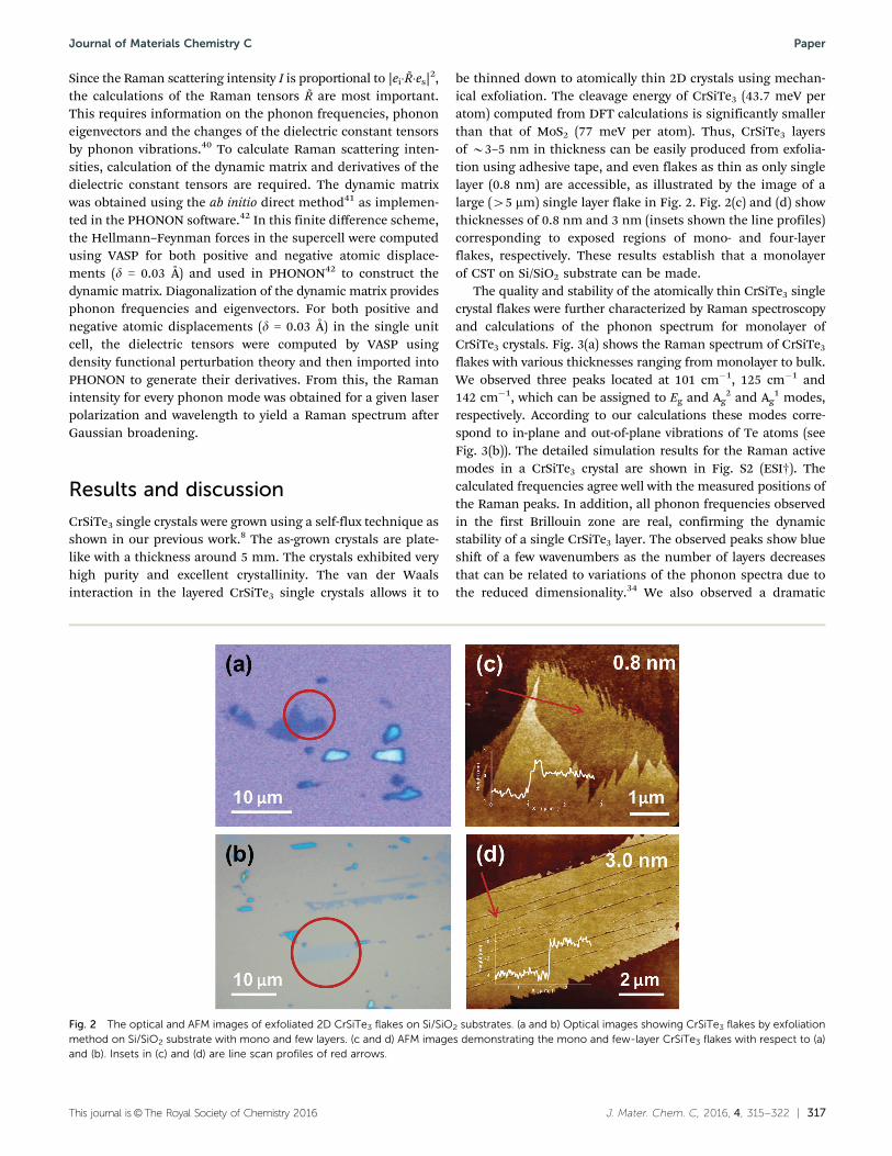
be thinned down to atomically thin 2D crystals using mechan-ical exfoliation. The cleavage energy of CrSiTe3 (43.7 meV peratom) computed from DFT calculations is significantly smallerthan that of MoS2 (77 meV per atom). Thus, CrSiTe3 layersof B3–5 nm in thickness can be easily produced from exfolia-tion using adhesive tape, and even flakes as thin as only singlelayer (0.8 nm) are accessible, as illustrated by the image of alarge (45 mm) single layer flake in Fig. 2. Fig. 2(c) and (d) showthicknesses of 0.8 nm and 3 nm (insets shown the line profiles)corresponding to exposed regions of mono- and four-layerflakes, respectively. These results establish that a monolayerof CST on Si/SiO2 substrate can be made.
The quality and stability of the atomically thin CrSiTe3 singlecrystal flakes were further characterized by Raman spectroscopyand calculations of the phonon spectrum for monolayer ofCrSiTe3 crystals. Fig. 3(a) shows the Raman spectrum of CrSiTe3
flakes with various thicknesses ranging from monolayer to bulk.We observed three peaks located at 101 cm"1, 125 cm"1 and142 cm"1, which can be assigned to Eg and Ag
2 and Ag1 modes,
respectively. According to our calculations these modes corre-spond to in-plane and out-of-plane vibrations of Te atoms (seeFig. 3(b)). The detailed simulation results for the Raman activemodes in a CrSiTe3 crystal are shown in Fig. S2 (ESI†). Thecalculated frequencies agree well with the measured positions ofthe Raman peaks. In addition, all phonon frequencies observedin the first Brillouin zone are real, confirming the dynamicstability of a single CrSiTe3 layer. The observed peaks show blueshift of a few wavenumbers as the number of layers decreasesthat can be related to variations of the phonon spectra due tothe reduced dimensionality.34 We also observed a dramatic
Fig. 2 The optical and AFM images of exfoliated 2D CrSiTe3 flakes on Si/SiO2 substrates. (a and b) Optical images showing CrSiTe3 flakes by exfoliationmethod on Si/SiO2 substrate with mono and few layers. (c and d) AFM images demonstrating the mono and few-layer CrSiTe3 flakes with respect to (a)and (b). Insets in (c) and (d) are line scan profiles of red arrows.
Journal of Materials Chemistry C Paper

318 | J. Mater. Chem. C, 2016, 4, 315--322 This journal is©The Royal Society of Chemistry 2016
change in the Raman spectra when the thickness decreasedfrom 7 nm to 3 nm, i.e., all three sharp peaks disappear andonly a broad feature at B160 cm"1 still remains in the spectra,but with much lower intensity. We also observed a dramaticchange in the Raman spectra starting at 7 nm thickness. Thepossible reason is that the spin ordering is changed along thesample thinning. The spin–lattice coupling is noticeable inCrSiTe3 and different spin states could lead to different latticeconstants,8 thus inducing different phonon frequencies. However,further studies on spin are needed.
We have fabricated 2D CrSiTe3 field-effect transistor (FET)devices using standard electron-beam lithography. Fig. 4(a)depicts a schematic diagram of the 2D CrSiTe3 FET device ona Si/SiO2 substrate with source/drain electrodes. The opticalmicrograph also demonstrates a clear image of the 2D CrSiTe3
FET device shown in Fig. 4(b). Although we are able to thinCrSiTe3 crystals down to a single layer, successful devices withgood electrical contacts can be prepared only on flakes withthickness Z7 nm. Based on the measurement of output curvesshown in Fig. 4(c) in a back-gating configuration, these CrSiTe3
FET devices display p-type semiconductor characteristics. Thelinear output curves indicate nearly Ohmic contacts at 295 Kand 6 K. Fig. 4(d) shows the Ids–Vbg transfer curves measured ona 7 nm thick CrSiTe3 device at different temperatures down to6 K with Vds = 1 V. The inset in Fig. 4(d) the mobility increasedwith temperature, demonstrating the same trend as found insingle layer MoS2 for the same gating configuration.43 Themobility (B0.01 cm2 V"1 s"1 at T = 295 K) was calculated using
the eqn m ¼ 1
Cox
L
WVds
! "dI
dVbg
! "extracted from the linear region
of the transport curves Ids–Vbg, where L is the channel length, Wis the channel width, Vds = 1 V and Cox = 1.2 ! 10"8 F cm"2 is
the capacitance between the channel and the back gate perunit area (Cox = e0er/dox, e0 = 8.85 ! 10"12 F m"1, er = 3.9 anddox = 290 nm).
The electronic band structure of monolayer CrSiTe3 wascalculated from first-principles calculations using DFT.Fig. 5(a) shows the spin-polarized electronic band structuresof monolayer CrSiTe3, confirming an indirect bandgap. Thebandgaps of FM ordering as a function of Ueff are presented inFig. S1(c) (ESI†). The gap sizes for spin-up and spin-down statesare 0.57 eV and 0.65 eV, respectively. For bulk CrSiTe3, usingthe same Ueff the calculated spin-up and spin-down bandgapsare 0.39 eV and 0.65 eV,8 respectively. The enhanced spin-upbandgap of monolayer CrSiTe3 compared to that of the bulk isdue to quantum confinement, which is an intrinsic property atlow dimensionality and similar to other 2D semiconductors.44,45
Furthermore, Fig. 5(b) shows the density of states of monolayerCrSiTe3, which illustrates that the Cr d and Te p orbitals areinvolved in superexchange interactions between the spins ofneighboring Cr3+ ions.
Table 1 provides a comparison between FM and AFMstructure, magnetic moment and formation energy as deter-mined by first-principles calculations for monolayer CrSiTe3. Ascan be seen, the lattice constants of monolayer CrSiTe3 withboth FM (6.69 Å) and AFM (6.66 Å) orderings are similar, as aretheir magnetic moments. The calculated magnetic momentsare 3.0 mB for both magnetic orderings. This value is the sameas the spin magnetic moment of an isolated Cr3+ ion, implyingthat the orbital magnetic moments are largely quenched inmonolayer CrSiTe3. Indeed, turning on spin–orbit coupling(SOC) in the calculation yields a similar total magnetic moment,which indicates a weak SOC. The ground state energy of mono-layer CrSiTe3 was calculated for both FM and AFM orderings.
Fig. 3 Measured Raman and phonon dispersion spectrum from first principles simulations for CrSiTe3 flakes. (a) Illustrates Raman spectrum of CrSiTe3
flakes with different thickness, showing the typical peaks at 142 cm"1, 125 cm"1 and 101 cm"1. The broad peak at 304 cm"1 belongs to Si. (b) The phononspectrum demonstrates the dynamic stablity for mono-layer CrSiTe3. The active Raman modes from simulation corresponding to Ag
1 (in-plane), Ag2 (out-
of-plane) and Eg (out-of-plane) of Te vibrations match the Raman peaks obtained from measurements.
Paper Journal of Materials Chemistry C

This journal is©The Royal Society of Chemistry 2016 J. Mater. Chem. C, 2016, 4, 315--322 | 319
The possible antiferromagnetic spin textures, Neel, stripy, andzigzag configurations, have been considered and computed(see Fig. S4, ESI†). Furthermore, we calculated the first, second,and third nearest-neighboring exchange constants with thecomputation details described in the ESI,† and determined J1,
J2, and J3 as "2.39 meV, 0.00 meV, and +0.18 meV, respectively.This suggests that the dominant exchange coupling comesfrom the first nearest-neighboring Cr–Cr pair interactions.Therefore, the energy of a FM monolayer CrSiTe3 is smallerthan the AFM one, showing that the ground-state monolayer
Fig. 5 Electronic band structure obtained from first-principles calculations using density-functional theory (DFT). (a) The electronic band structuresof spin-up and spin-down is denoted as blue and red. (b) Spin density of states show the bandgap of monolayer of CiSiTe3 with the gap size 0.57 eV and0.65 eV for spin up and spin down, respectively.
Fig. 4 Schematic diagram, optical micrograph and characteristics of a CrSiTe3 FET device. (a) Schematic of a CrSiTe3 FET device on Si/SiO2 substrateshowing the source/drain electrodes. (b) OM image showing top view of CrSiTe3 FET devices with electrodes. (c) Ids–Vds output curves are nearly linearsuggesting the device contacts are essentially Ohmic at 295 K. Inset is the Ids–Vds curves at 6 K. (d) The transfer curve shows p-type semiconductorbehavior down to 6 K. The mobility as a function of temperature for a 7.0 nm thick CrSiTe3 FET device in the inset, indicating the mobility decreases asdecreasing temperature.
Journal of Materials Chemistry C Paper

320 | J. Mater. Chem. C, 2016, 4, 315--322 This journal is©The Royal Society of Chemistry 2016
CrSiTe3 exhibits ferromagnetic ordering. In addition, we car-ried out similar calculations of exchange coupling constants forp-type doped single-layer CrSiTe3 by using a 2 ! 2 supercellmodel with 0.155 electrons removed from the same supercell ofpristine single-layer CrSiTe3 with 288 electrons. This is equiva-lent to p-type doping with a very high hole concentration of 1013
cm"2. From Fig. S4(f) (ESI†), we can see that the FM structure isstill the ground state. Following the same procedure, we obtainthe exchange coupling parameters of"2.39 meV, 0.02 meV, and+0.18 meV, which are nearly identical to those in the undopedcase. This suggests that p-type doping almost has no effect onthe Curie temperature.
Another important characteristic of the 2D CrSiTe3 materialis ferromagnetism perseverance in low dimensionality withchanging Curie temperature Tc. The Tc change has been reportedin other multilayered systems from 3D to 2D.21–22,46,47 From ourtheoretical calculations using a 2D Ising model, Tc can reachvalues up to B80 K for monolayer CrSiTe3 with a magneticmoment of 3 mB as shown in Fig. 6(a). The inset of Fig. 6(a) showsthe susceptibility as a function of temperature for monolayerCrSiTe3. The higher Tc in monolayer CrSiTe3 can be understoodas possibly resulting from the competition between interlayerand intralayer exchange interactions compared with bulk. Theexchange coupling interaction becomes dominated by intralayerCr–Cr superexchange mediated by Te ions as one proceedstoward a monolayer of CrSiTe3, which gives higher in-planeinteraction energy associated with higher Tc. Theoretical calcula-tions also indicate higher energy for exchange coupling resultingfrom intralayer versus interlayer interactions. The resistivity
measured for a 7 nm thick 2D CrSiTe3 device shown inFig. 6(b) is seen to increase exponentially with decreasingtemperature in the high temperature regime, but then clearlydeviates from this behavior starting at 140 K. We found that theresistivities measured between 100–140 K significantly deviatedfrom the average value below 100 K (shown by the dashed linein Fig. 6(b)) which we attribute to instrumental resolution. Verysimilar resistivity versus temperature was measured for deviceswith thicknesses of 8.5 nm and 20 nm (shown in Fig. S3, ESI†).Altogether, the devices showed transitions from the expectedexponential increase in resistivity with decreasing temperature,with clear and measurable deviations from this behavior attemperatures ranging between 80–120 K (shown by arrows inFig. S3, ESI†). Some published results on metal thin filmsystems have shown that the critical temperature of a FM toAFM phase transition is accompanied by an abrupt change inresistivity at that temperature due to scattering caused by achange of magnetic moments.48,49 In our data, the abrupttransition temperature for the resistivity is generally found todecrease with decreasing number of layers, which we believe islikely due to changes in magnetic ordering with reducing dimen-sionality. This explanation relies upon the plausible existence ofAFM or FM ordering in 2D magnetic semiconductors down to verythin layers. However, absolute proof of the magnetization ofmonolayer CrSiTe3 by SQUID measurements is currently extremelycomplicated due to a very weak signal and the difficulty inpreparing uniform 2D flakes using mechanical exfoliation.Such measurements will be the subject of future studies.
ConclusionsIn conclusion, monolayer and few-layer samples of 2D FMCrSiTe3 crystals were isolated after exfoliation and character-ized by Raman spectroscopy, allowing the identification of theRaman-active modes predicted from the calculated phonon spectraand confirming the theoretical predictions that monolayer CrSiTe3
Table 1 Comparison between ferromagnetic (FM) and antiferromagnetic(AFM) structure (lattice constant a0), magnetic moment mB, and formationenergy Ef for monolayer CrSiTe3
a0 (Å) m (mB) Ef
FM 6.69 3.0 43.7AFM 6.66 3.0 48.7
Fig. 6 (a) The calculated transition temperature (Tc) with magnetic moment 3 mB for monolayer CrSiTe3 using 2D Ising model Monte Carlo simulationswith the exchange parameter from the LDA+U calculations. Inset shows the susceptibility as function of temperature for monolayer CrSiTe3. (b) The plotof logarithmic resistivity vs. temperature for a CrSiTe3 flake of 7 nm thickness, exhibiting an expected increase in resisitivity with decreasing temperaturein the high temperature regime, but with a clear deviation from this behavior beginning B140 K, indicating a possible FM–AFM phase transition at thattemperature. The dashed line indicates the average resistivity for measurements T o 100 K.
Paper Journal of Materials Chemistry C

This journal is©The Royal Society of Chemistry 2016 J. Mater. Chem. C, 2016, 4, 315--322 | 321
is dynamically stable. The exfoliated few-layer samples retainedthe p-type semiconductor characteristics of bulk CrSiTe3, ascharacterized by FET devices fabricated from the lithographically-addressed 2D crystals. Ising model calculations predicted anelevated Curie temperature (Tc B 80 K) for the magneticordering of monolayer 2D CrSiTe3 crystals, significantlyincreased from the bulk (Tc B 33 K). Consistent with thesepredictions, temperature-dependent resistivity measurementsfor the few-layer 2D CrSiTe3 FET devices indicate a clear changein resistivity at elevated temperatures of 80–120 K. These resultsindicate that ferromagnetic mono- and few-layer 2D CrSiTe3
crystals are promising ultrathin nanomaterials for potentialapplications in spintronics.
AcknowledgementsDevice fabrication was supported by the Laboratory DirectedResearch and Development program (LDRD) project andRaman measurements were conducted at Center for Nano-phase Materials Sciences, which is sponsored at Oak RidgeNational Laboratory by the Scientific User Facilities Division,Office of Basic Energy Sciences, U.S. Department of Energy.DGM and JQY acknowledge support from the National ScienceFoundation under Grant No. NSF DMR-1410428. TZW acknow-ledge support from the US Department of Energy (DOE), Office ofBasic Energy Sciences (BES), Materials Sciences and EngineeringDivision for PPMS measurements. HZ, PG, PRCK acknowledgesupport from LDRD project for theoretical calculations. LLwas supported as a Eugene P. Wigner Fellow at Oak RidgeNational Laboratory.
Notes and references1 Q. H. Wang, K. Kalantar-Zadeh, A. Kis, J. N. Coleman and
M. S. Strano, Nat. Nanotechnol., 2012, 7, 699–712.2 A. K. Geim and I. V. Grigorieva, Nature, 2013, 499, 419–425.3 V. Nicolosi, M. Chhowalla, M. G. Kanatzidis, M. S. Strano
and J. N. Coleman, Science, 2013, 340, 1226419.4 S. Lebegue, T. Bjorkman, M. Klintenberg, R. Nieminen and
O. Eriksson, Phys. Rev. X, 2013, 3, 031002.5 B. Sachs, T. O. Wehling, K. S. Novoselov, A. I. Lichtenstein
and M. I. Katsnelson, Phys. Rev. B: Condens. Matter Mater.Phys., 2013, 88, 201402.
6 N. Sivadas, M. W. Daniels, R. H. Swendsen, S. Okamoto andD. Xiao, Phys. Rev. B: Condens. Matter Mater. Phys., 2015,91, 235425.
7 V. Carteaux, G. Ouvrard, J. C. Grenier and Y. Laligant,J. Magn. Magn. Mater., 1991, 94, 127–133.
8 L. D. Casto, A. J. Clune, M. O. Yokosuk, J. L. Musfeldt, T. J.Williams, H. L. Zhuang, M.-W. Lin, K. Xiao, R. G. Hennig,B. C. Sales, J.-Q. Yan and D. Mandrus, APL Mater., 2015,3, 041515.
9 H. Kabbour, R. David, A. Pautrat, H.-J. Koo, M.-H. Whangbo,G. Andre and O. Mentre, Angew. Chem., Int. Ed., 2012, 51,11745–11749.
10 M. A. McGuire, H. Dixit, V. R. Cooper and B. C. Sales, Chem.Mater., 2015, 27, 612–620.
11 I. Yamada, J. Phys. Soc. Jpn., 1972, 33, 979–988.12 S. Tongay, S. S. Varnoosfaderani, B. R. Appleton, J. Wu and
A. F. Hebard, Appl. Phys. Lett., 2012, 101, 123105.13 Z. Zhang, X. Zou, V. H. Crespi and B. I. Yakobson, ACS Nano,
2013, 7, 10475–10481.14 H. Pan and Y.-W. Zhang, J. Phys. Chem. C, 2012, 116,
11752–11757.15 S. Yang, C. Wang, H. Sahin, H. Chen, Y. Li, S.-S. Li, A. Suslu,
F. M. Peeters, Q. Liu, J. Li and S. Tongay, Nano Lett., 2015,15, 1660–1666.
16 M. N. Ali, J. Xiong, S. Flynn, J. Tao, Q. D. Gibson, L. M.Schoop, T. Liang, N. Haldolaarachchige, M. Hirschberger,N. P. Ong and R. J. Cava, Nature, 2014, 514, 205–208.
17 L. Cai, J. He, Q. Liu, T. Yao, L. Chen, W. Yan, F. Hu, Y. Jiang,Y. Zhao, T. Hu, Z. Sun and S. Wei, J. Am. Chem. Soc., 2015,137, 2622–2627.
18 N. Mermin and H. Wagner, Phys. Rev. Lett., 1966, 17,1133–1136.
19 P. Bruno, Phys. Rev. Lett., 2001, 87, 137203.20 M. Pomerantz, Surf. Sci., 1984, 142, 556–570.21 Y. Li and K. Baberschke, Phys. Rev. Lett., 1992, 68, 1208–1211.22 M. A. Medvedeva and P. V. Prudnikov, J. Phys.: Conf. Ser.,
2014, 510, 012024.23 M. Osada, Y. Ebina, K. Fukuda, K. Ono, K. Takada,
K. Yamaura, E. Takayama-Muromachi and T. Sasaki, Phys.Rev. B: Condens. Matter Mater. Phys., 2006, 73, 153301.
24 X. Zhang, J. Zhang, J. Zhao, B. Pan, M. Kong, J. Chen andY. Xie, J. Am. Chem. Soc., 2012, 134, 11908–11911.
25 T. Taniguchi, K. Yamaguchi, A. Shigeta, Y. Matsuda,S. Hayami, T. Shimizu, T. Matsui, T. Yamazaki, A. Funatstu,Y. Makinose, N. Matsushita, M. Koinuma and Y. Matsumoto,Adv. Funct. Mater., 2013, 23, 3140–3145.
26 M. Osada, S. Yoguchi, M. Itose, B.-W. Li, Y. Ebina,K. Fukuda, Y. Kotani, K. Ono, S. Ueda and T. Sasaki,Nanoscale, 2014, 6, 14227–14236.
27 G. Ouvrard, E. Sandre and R. Brec, J. Solid State Chem., 1988,73, 27–32.
28 V. Carteaux, F. Moussa and M. Spiesser, EPL, 1995, 29,251–256.
29 T. J. Williams, A. A. Aczel, M. D. Lumsden, S. E. Nagler, M. B.Stone, J.-Q. Yan and D. Mandrus, 2015, arXiv: 1503.08199v1.
30 X. Li and J. Yang, J. Mater. Chem. C, 2014, 2, 7071–7076.31 X. Chen, J. Qi and D. Shi, Phys. Lett. A, 2015, 379, 60–63.32 H. L. Zhuang, Y. Xie, P. R. C. Kent and P. Ganesh, Phys. Rev.
B: Condens. Matter Mater. Phys., 2015, 92, 035407.33 X. Wang, Y. Gong, G. Shi, W. L. Chow, K. Keyshar, G. Ye,
R. Vajtai, J. Lou, Z. Liu, E. Ringe, B. K. Tay and P. M. Ajayan,ACS Nano, 2014, 8, 5125–5131.
34 X. Li, M.-W. Lin, A. A. Puretzky, J. C. Idrobo, C. Ma, M. Chi,M. Yoon, C. M. Rouleau, I. I. Kravchenko, D. B. Geoheganand K. Xiao, Sci. Rep., 2014, 4, 5497.
35 K. S. Novoselov, A. K. Geim, S. V. Morozov, D. Jiang,Y. Zhang, S. V. Dubonos, I. V. Grigorieva and A. A. Firsov,Science, 2004, 306, 666–669.
Journal of Materials Chemistry C Paper

322 | J. Mater. Chem. C, 2016, 4, 315--322 This journal is©The Royal Society of Chemistry 2016
36 X. Li, X. Wu and J. Yang, J. Am. Chem. Soc., 2014, 136,11065–11069.
37 G. Kresse and J. Furthmuller, Comput. Mater. Sci., 1996, 6,15–50.
38 G. Kresse and D. Joubert, Phys. Rev. B: Condens. MatterMater. Phys., 1999, 59, 1758–1775.
39 A. I. Liechtenstein, V. I. Anisimov and J. Zaanen, Phys. Rev.B: Condens. Matter Mater. Phys., 1995, 52, R5467–R5470.
40 L. Liang and V. Meunier, Nanoscale, 2014, 6, 5394–5401.41 K. Parlinski, Z. Q. Li and Y. Kawazoe, Phys. Rev. Lett., 1997,
78, 4063–4066.42 K. Parlinski, Computer Code PHONON, Krakow, Poland, 2010.43 B. Radisavljevic and A. Kis, Nat. Mater., 2013, 12, 815–820.
44 G. W. Mudd, S. A. Svatek, T. Ren, A. Patane, O. Makarovsky,L. Eaves, P. H. Beton, Z. D. Kovalyuk, G. V. Lashkarev,Z. R. Kudrynskyi and A. I. Dmitriev, Adv. Mater., 2013, 25,5714–5718.
45 Y. Yoon, K. Ganapathi and S. Salahuddin, Nano Lett., 2011,11, 3768–3773.
46 A. Du and G. Wei, Aust. J. Phys., 1993, 46, 571–582.47 L. Capriotti, R. Vaia, A. Cuccoli and V. Tognetti, Phys. Rev. B:
Condens. Matter Mater. Phys., 1998, 58, 273–281.48 J. S. Kouvel and C. C. Hartelius, J. Appl. Phys., 1962, 33,
1343–1344.49 M. A. D. Vries, M. Loving, A. P. Mihai, L. H. Lewis, D. Heiman
and C. H. Marrows, New J. Phys., 2013, 15, 013008.
Paper Journal of Materials Chemistry C