phonon manipulation with phononic crystals
TRANSCRIPT

SANDIA REPORT SAND2012-0127 Unlimited Release Printed January and 2012
Phonon Manipulation with Phononic Crystals
Ihab El-Kady, Roy H. Olsson III, Patrick E. Hopkins, Zayd C. Leseman, Drew F. Goettler, Bongsang Kim, Charles M. Reinke, and Mehmet F. Su
Prepared by Sandia National Laboratories Albuquerque, New Mexico 87185 and Livermore, California 94550
Sandia National Laboratories is a multi-program laboratory managed and operated by Sandia Corporation, a wholly owned subsidiary of Lockheed Martin Corporation, for the U.S. Department of Energy's National Nuclear Security Administration under contract DE-AC04-94AL85000. Approved for public release; further dissemination unlimited.

2
Issued by Sandia National Laboratories, operated for the United States Department of Energy
by Sandia Corporation.
NOTICE: This report was prepared as an account of work sponsored by an agency of the
United States Government. Neither the United States Government, nor any agency thereof,
nor any of their employees, nor any of their contractors, subcontractors, or their employees,
make any warranty, express or implied, or assume any legal liability or responsibility for the
accuracy, completeness, or usefulness of any information, apparatus, product, or process
disclosed, or represent that its use would not infringe privately owned rights. Reference herein
to any specific commercial product, process, or service by trade name, trademark,
manufacturer, or otherwise, does not necessarily constitute or imply its endorsement,
recommendation, or favoring by the United States Government, any agency thereof, or any of
their contractors or subcontractors. The views and opinions expressed herein do not
necessarily state or reflect those of the United States Government, any agency thereof, or any
of their contractors.
Printed in the United States of America. This report has been reproduced directly from the best
available copy.
Available to DOE and DOE contractors from
U.S. Department of Energy
Office of Scientific and Technical Information
P.O. Box 62
Oak Ridge, TN 37831
Telephone: (865) 576-8401
Facsimile: (865) 576-5728
E-Mail: [email protected]
Online ordering: http://www.osti.gov/bridge
Available to the public from
U.S. Department of Commerce
National Technical Information Service
5285 Port Royal Rd.
Springfield, VA 22161
Telephone: (800) 553-6847
Facsimile: (703) 605-6900
E-Mail: [email protected]
Online order: http://www.ntis.gov/help/ordermethods.asp?loc=7-4-0#online

3
SAND2012-0127
Unlimited Release
Printed January 2012
Phonon Manipulation with Phononic Crystals
Ihab El-Kady and Charles M. Reinke
Photonic Microsystems Technologies Department
Roy H. Olsson III, Zayd C. Leseman, Drew F. Goettler, and Bongsang Kim
MEMS Technologies Department
Patrick E. Hopkins
Microscale Science & Technology Department
Sandia National Laboratories
P.O. Box 5800
Albuquerque, New Mexico 87185-MS1082
Mehmet F. Su
Mechanical Engineering Department
University of New Mexico
1 University of New Mexico
Albuquerque, New Mexico 87131-0001
Abstract
In this work, we demonstrated engineered modification of propagation of thermal
phonons, i.e. at THz frequencies, using phononic crystals. This work combined
theoretical work at Sandia National Laboratories, the University of New Mexico, the
University of Colorado Boulder, and Carnegie Mellon University; the MESA
fabrication facilities at Sandia; and the microfabrication facilities at UNM to produce
world-leading control of phonon propagation in silicon at frequencies up to 3 THz.
These efforts culminated in a dramatic reduction in the thermal conductivity of silicon
using phononic crystals by a factor of almost 30 as compared with the bulk value, and
about 6 as compared with an unpatterned slab of the same thickness.

4
ACKNOWLEDGMENTS
The Principle Investigator, Ihab El-Kady, would like to thank Mahmoud Hussein, Alan
McGaughey, Eric Shaner, Bruce Davis, Charles Harris, Thomas Beechem, Khalid Hattar, Janet
Nguyen, Yasser Soliman, and Maryam Ziaei-Moayyed for their contributions to this research.
Their efforts were invaluable in making this project a success.

5
CONTENTS
1. Introduction .............................................................................................................................. 11 1.1. Thermoelectrics............................................................................................................. 11
1.2.1. Thermoelectric Basics ..................................................................................... 11 1.2.1. Challenges to Current TE Technologies ......................................................... 14
1.2. Thermal Conductivity Applications of Phononic Crystals ........................................... 15
2. Calculation of the Thermal Conductivity of Phononic Crystals .............................................. 19 2.1. Callaway-Holland Methods .......................................................................................... 19 2.2. Bloch Mode Plane-Wave Expansion Technique .......................................................... 21 2.3. Lattice Dynamics Technique ........................................................................................ 24
2.4. Thermal Conductivity Calculations .............................................................................. 25
2.4.1. Density of States Method ................................................................................ 25
2.4.2. DOS with Slab Padding .................................................................................. 27 2.4.3. Dispersion Method with Mode Velocities ...................................................... 28
2.4.4. Multi-Scale Method ........................................................................................ 29
3. Fabrication of Phononic Crystal Devices ................................................................................ 31
3.1. MESA Silicon-Fab ........................................................................................................ 31 3.2. Focused Ion Beam......................................................................................................... 33
4. Characterization of Thermoelectric Figure-of-Merit ............................................................... 39
4.1. In-Plane Measurement Techniques ............................................................................... 39 4.1.1. Equilibrium Thermoelectric Measurements ................................................... 39
4.1.2. Suspended Island Technique ........................................................................... 42 4.2. Cross-Plane Thermal Conductivity Measurement ........................................................ 47
4.1.2. Time Domain Thermoreflectance Technique ................................................. 47 4.2.1. Cross-Plane TDTR .......................................................................................... 47
4.2.2. In-Plane TDTR................................................................................................ 54
5. Results ...................................................................................................................................... 55 5.1. Experimental Measurements ......................................................................................... 55
5.1.1. Measurement of Thermal and Electrical Conductivity Reduction in PnCs .... 55
5.1.2. Dependence of Thermal Conductivity on Lattice Type and Topology .......... 61 5.1.3. Full ZT Characterization of PnC Samples ...................................................... 62
6. Conclusions and Future Outlook ............................................................................................. 67
7. References ................................................................................................................................ 69
Appendix A: Publications, Conferences, and Awards ................................................................. 73
A.1. Journal Publications ...................................................................................................... 73 A.2. Conferences................................................................................................................... 73
A.2.1. Organized Conferences ................................................................................... 73 A.2.2. Conference Presentations ................................................................................ 73
A.1. Patents ........................................................................................................................... 76
Distribution ................................................................................................................................... 77

6
FIGURES
Figure 1. A schematic diagram of a thermoelectric power generator. ......................................... 11 Figure 2. A schematic diagram of a thermoelectric cooler. ......................................................... 12 Figure 3. Phononic crystal concept: a) Schematic of the phonon distribution in a bulk material.
b) Schematic of the phonon distribution in a 2D PnC structure. c) Conceptual visualization of
Bragg and Mie resonance scattering. d) SEM image of a fabricated PnC consisting of a square
array of tungsten rods in a Si membrane; a is the lattice constant, r is the radius of the tungsten
rods, and t is the membrane thickness (not shown in image). ...................................................... 15 Figure 4. a) Right panel shows the calculated band structure for a PnC composed of air holes in
a Si matrix (blue) compared with the band structure f an unpatterned Si slab (red) of the same
thickness ―t‖. Left panel shows the corresponding PnC density of states (DOS). b) The
integrated density of photon states for the PnC and Si slabs for the exemplar case of a = 500 nm,
r/a = 0.3, and t/a = 1.0, where a is the lattice constant, r is the radius of the air hole and t is the
slab thickness. ............................................................................................................................... 16 Figure 5. Classification of phonon spectrum. ............................................................................. 17
Figure 6. Schematic of a TE PnC thermoelectric device. ........................................................... 18 Figure 7. Illustration of the computation domain used for the supercell PWE calculation, with air
layers above and below the Si PnC later (red). The actual unit cell used in the simulations is
shown in blue. ............................................................................................................................... 23 Figure 8. Bandgap map versus hole radius for a PnC composed of air holes in Si for various slab
thicknesses. ................................................................................................................................... 24 Figure 9. Phononic dispersion of bulk Si for Γ–Χ (black curves), along with the corresponding
dispersion from the Debye approximation for transverse (red dashed curve) and longitudinal
(blue dashed curve) modes. ........................................................................................................... 26
Figure 10. The thermal conductivity of Si structures at room temperature as a function of L for
the PnCs (unfilled squares), microporous solids (filled pentagons), nanomesh (filled diamond),
and a suspended 500 nm thick Si films that is, an unpatterned Si slab (unfilled circle). The
references are from [26]. The solid line represents predictions of the unpatterned slab at room
temperature as a function of L. The dashed line represents predictions of the PnC thermal
conductivity using DOS data from PWE calculations. ................................................................. 27 Figure 11. Integrated DOS for a Si slab of 500 nm thickness and a PnC of the same thickness
and with 150 nm radius air holes. ................................................................................................. 28 Figure 12. A schematic of the thermal conductivity test structure design. A phononic crystal
bridge is suspended from the substrate. Serpentine aluminum traces are installed at both the
bridge center and both bridge ends. While heat is supplied at the center, the temperature gradient
across the bridge is measured to extract device thermal characteristics. ...................................... 32
Figure 13. Schematics of the fabrication process for the thermal conductivity measurement
structures. ...................................................................................................................................... 32 Figure 14. SEM images of fabricated simple cubic (SC) phononic crystal thermal conductivity
test devices. ................................................................................................................................... 33
Figure 15. Schematic of a focused ion beam (FIB) system. Ions are extracted and then focused
by multiple apertures and electromagnetic fields onto a sample. All of the FIB components and
sample are under vacuum to prevent degradation. (Image courtesy of FEI) ............................... 33

7
Figure 16. Drawing of a liquid metal ion source. Liquid metal wets a sharp tip and an extractor
lens extracts ions from the metal by using a high accelerating voltage in the kV range. ............. 34 Figure 17. Sputter rates for various materials as a function of angle. Incident ion is Ga
+ at 30kV.
Sputter rates were calculated using a Monte Carlo simulation package named TRIM. Solid black
lines are interpolated values. ......................................................................................................... 35 Figure 18. Fabrication process for creating a thin-freestanding membrane for PnCs. a) Cross
sectional view of fabrication process. b) Released freestanding membrane. .............................. 36 Figure 19. Second fabrication method for creating a thin-freestanding PnC. a) Cross sectional
view of fabrication process. b) Released freestanding PnC. ......................................................... 36
Figure 20. 30kV Ga+ ion penetration into 50 nm thick layer of Ni on top of 50 nm layer of Si.
No ions reach the Si layer. ............................................................................................................ 37 Figure 21. Trace resistance vs. temperature calibration data from a heated chuck measurement.
a) Measured resistance values of heater trace and sensor trace with changing temperature. b) For
both heater and sensor traces, their relative resistance changes were almost identical. The slope
of this line is 0.0027. ..................................................................................................................... 39
Figure 22. Test setup diagram for thermal conductivity measurement. ...................................... 40 Figure 23. An example plot of measured temperature vs. heating power plot (Device ID-7).
Temperature difference across the phononic crystal bridge was measured using calibrated
serpentine traces while heating power supplied at the bridge center was sweeping between 0 to 1
mW. ............................................................................................................................................... 40
Figure 24. a) ANSYS FEM simulation model and b) equivalent thermal circuit model of thermal
conductivity test structures. .......................................................................................................... 41
Figure 25. An example of extracted thermal conductivity values using the models shown in
Figure 24. At low heating power, the data are scattered. In this study, thermal conductivities
values at 300 K were used, which were more reliable and repeatable. Red circles indicate when
the temperature was ramping up and blue circles when ramping down. This plot is the measured
data of Device ID-7. ...................................................................................................................... 42 Figure 26. SEM images of multi-use test platform for measuring thermal conductivity of
phononic crystals. Both images are tilted 52° with respect to normal. a. Overview of suspended
islands. b. Zoom-in of the SiNx bridge connecting the heater and sensing islands. Pt pads on
either side of the bridge provide a location for the PnCs to be welded on to the islands. ............ 43
Figure 27. Process flow for fabrication of in-plane thermal conductivity test platform. ............. 43 Figure 28. SEM images of PnCs measured with multi-use platform. a. Simple cubic PnC. b.
Hexagonal PnC. ............................................................................................................................ 44 Figure 29. PnC mounted onto a thermal conductivity platform. ................................................. 45 Figure 30. Electrical and Thermal Circuit of test platform. ......................................................... 46 Figure 31. Schematic of TDTR experiment built at Sandia as part of this LDRD. ..................... 51 Figure 32. TDTR data from a 117 nm Al film evaporated on a Si substrate along with the best fit
from the thermal model. The thermophysical properties determined from the model best fits are
hK = 210 MW m-2
K-1
for the Al/Si interface and = 141 W m-1
K-1
for the Si substrate. .......... 53
Figure 33. Thermal sensitivities in TDTR to hK and of the substrate in 100 nm Al/Si and
Al/SiO2 systems. ........................................................................................................................... 53 Figure 34. The steps of image processing for the hole size measurement. a) SEM images
containing 16~20 holes were taken. b) Complementary images were made. c) By setting the
gray threshold, the hole boundaries are determined and the number of white pixels were counted
to calculated hole areas and diameters. ......................................................................................... 56

8
Figure 35. Measured thermal conductivity values. The control device (Device ID-1), which has
no holes, measured km = 104 W m-1
K-1
; this is consistent with literature values for 500 nm-thick
single crystal silicon. ..................................................................................................................... 56 Figure 36. a) ANSYS FEM simulation for the effective conductivity reduction by introducing
periodic holes. b) Volume reduction effect factors comparison between ANSYS FEM
simulation model and Maxwell-Eucken model. ........................................................................... 57 Figure 37. Comparison between km/km,control (relative thermal conductivity with respect to the
control device), σm/ σm,control (relative electrical conductivity with respect to the control device),
and FFEM (reduction effect factor from ANSYS FEM). The measured σm/ σm,control match very
well with FFEM for all Device IDs; some data points are difficult to distinguish because they
exactly overlap with each other. However, the km/km,control ratios are much smaller than FFEM for
all cases, inferring a reduction in the thermal conductivity that is beyond the contribution from
the volume reduction effect. ......................................................................................................... 58
Figure 38. Comparison of kn versus limiting dimension with the same lattice constant. As the
limiting dimension decreases, the kn decreases, which indicates that incoherent scattering plays a
significant role to reduce thermal conductivity of phononic crystals. Numbers adjacent the data
points are the Device IDs. Each data point is averaged from 6 measured devices. ..................... 59
Figure 39. Comparison of kn versus lattice constant with the same limiting dimension. Even
with the same limiting dimensions, kn decreases, as the lattice constant increases, which infers
that incoherent scattering is not the only mechanism for the thermal conductivity reduction.
Numbers adjacent the data points are the Device IDs. Each data point is averaged from 6
measured devices. ......................................................................................................................... 60
Figure 40. Hypothetical schematic explaining coherent scattering enhancement at a given
limiting dimension. As the lattice constant increases, the two Bragg resonant frequencies
approach each other, opening a phononic bandgap at some point which widens as the lattice
constant increases.......................................................................................................................... 60
Figure 41. Calibration data from a test platform. Black refers to the heater island and blue refers
to the sensor island. Both the heater and sensor showed linear trends across a 40° C temperature
range. ............................................................................................................................................. 61
Figure 42. Plot of input power vs. heater resistance for the hexagonal PnC. .............................. 62 Figure 43. A schematic of the ZT measurement test structure design. A phononic crystal bridge
is suspended from the substrate. One half of the bridge is doped n-type while the other half is
doped p-type. Electrical contacts are provided at the bridge ends to measure the amount of
thermoelectrically induced current and voltage when heat is supplied at the bridge center. ........ 63 Figure 44. Schematics of the fabrication process for the ZT measurement structures. ............... 64 Figure 45. Sumary of predicted ZT enhancement for the fabricated PnC devices. ..................... 65
TABLES
Table 1. Material parameters used in PWE simulations of Si PnCs ............................................ 24 Table 2. Summary of designed hole pitches and diameters. ........................................................ 55
Table 3. Summary of the measured thermal conductivity values (300 K). ................................. 56 Table 4. Comparison between km/km,control (relative thermal conductivity with respect to the
control device), σm/σm,control (relative electrical conductivity with respect to the control device),
and FFEM (modeled volume reduction effect from ANSYS FEM). .............................................. 58

9
Table 5. Summary of kn, relative thermal conductivity values (km/km,control) normalized by
ANSYS FEM volume reduction effect factors (FFEM). ................................................................. 59 Table 6. Results of thermal conductivity for hexagonal and simple cubic PnC .......................... 62

10
NOMENCLATURE
DOS density of states
IBZ irreducible Brillouin zone
FEM finite element modeling
FIB focused ion beam
LD lattice dynamics
MEMS microelectromechanical systems
PnC photonic crystal
PWE plane-wave expansion
RLV reciprocal lattice vector
RTD resistance temperature detector
SEM scanning electron microscope
SNL Sandia National Laboratories
SOI silicon-on-insulator
TCR temperature coefficient of resistance
TDTR time domain thermoreflectometry
TE thermoelectric
ZT dimensionless thermoelectric figure-of-merit
11
1. INTRODUCTION
1.1. Thermoelectrics
1.2.1. Thermoelectric Basics
The thermoelectric effect is defined as the process whereby a sustained temperature gradient
across a material generates a proportional electric potential difference, and vice versa. On an
atomic scale the effect can be understood by noting that an applied temperature gradient causes
charged carriers in the material to diffuse from the hot side to the cold side in accordance with
the second law of thermodynamics hence inducing a thermal current and consequently a
potential difference. Such a phenomenon can thus be used to transform heat into electricity, in
which case it is commonly referred to as the ―Peltier effect‖ and has the potential to enable the
recycling of waste heat or thermal energy, a natural outcome of almost all artificial and natural
processes, to the more useful form of electrical energy. While the thermoelectric effect can and
was initially observed in metals, we are particularly interested in the case where the material in
use is a semiconductor for reasons that will become self-evident later on in our discussions.
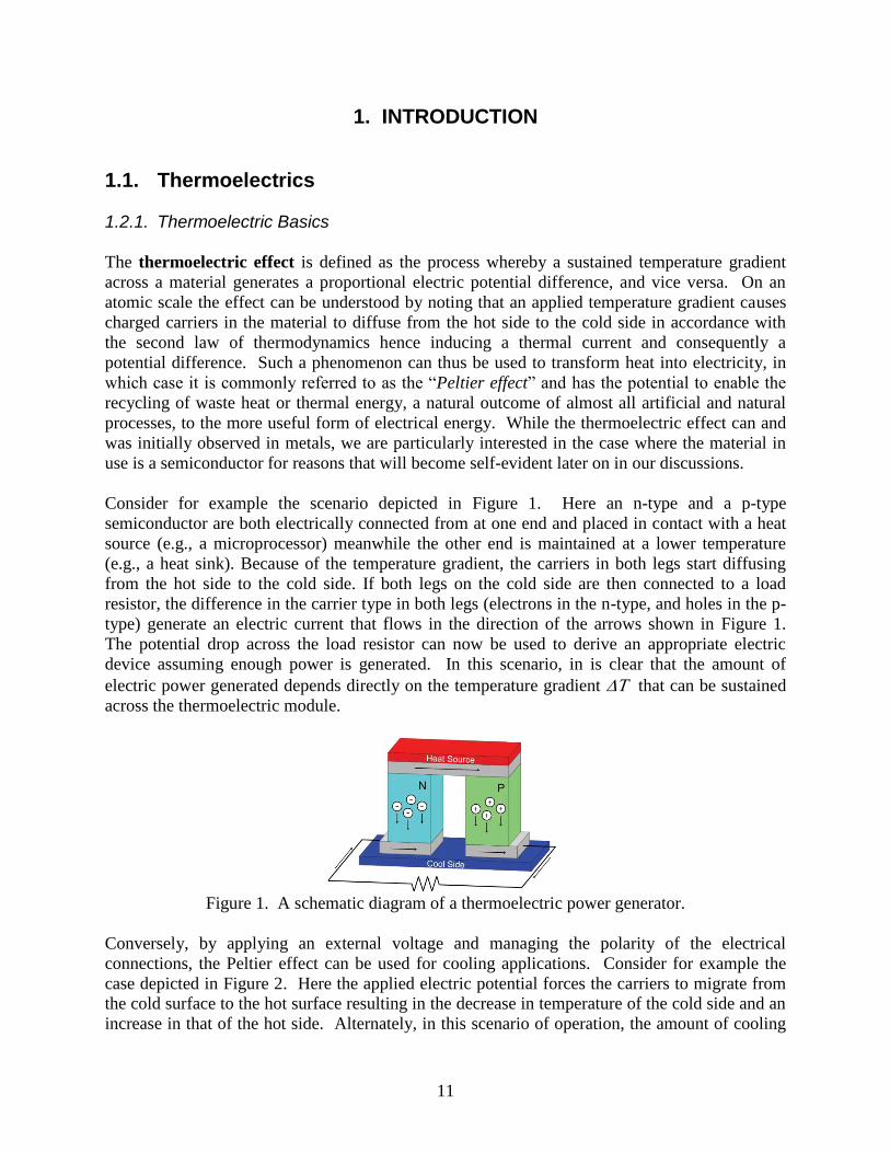
Consider for example the scenario depicted in Figure 1. Here an n-type and a p-type
semiconductor are both electrically connected from at one end and placed in contact with a heat
source (e.g., a microprocessor) meanwhile the other end is maintained at a lower temperature
(e.g., a heat sink). Because of the temperature gradient, the carriers in both legs start diffusing
from the hot side to the cold side. If both legs on the cold side are then connected to a load
resistor, the difference in the carrier type in both legs (electrons in the n-type, and holes in the p-
type) generate an electric current that flows in the direction of the arrows shown in Figure 1.
The potential drop across the load resistor can now be used to derive an appropriate electric
device assuming enough power is generated. In this scenario, in is clear that the amount of
electric power generated depends directly on the temperature gradient that can be sustained
across the thermoelectric module.
Figure 1. A schematic diagram of a thermoelectric power generator.
Conversely, by applying an external voltage and managing the polarity of the electrical
connections, the Peltier effect can be used for cooling applications. Consider for example the
case depicted in Figure 2. Here the applied electric potential forces the carriers to migrate from
the cold surface to the hot surface resulting in the decrease in temperature of the cold side and an
increase in that of the hot side. Alternately, in this scenario of operation, the amount of cooling

12
or temperature drop on the cold side is directly proportional to the applied electric voltage, which
also directly depends on the temperature difference between the hot and the cold sides of the
thermoelectric module.
Figure 2. A schematic diagram of a thermoelectric cooler.
Whether the thermoelectric (TE) device is operated as a cooler or a power generator, it is evident
that the ability to mold and control the direction of motion of the charge carriers in the system is
key to the operation of the TE device. In fact the performance of a material’s efficacy for use in a
TE setting is often quantified by the dimensionless figure of merit, ZT [1-3]:
,2
TS
ZT
(1)
where S is the Seebeck coefficient, σ is the electrical conductivity, κ is the thermal conductivity
and T is the temperature. For an actual TE module with both n-type and p-type legs, the
expression for the figure of merit is slightly more complicated and takes on the form:
.
)(
2
2
nnnn
np TSSTZ
(2)
Here, the subscripts n and p denote the semiconductor leg-type, and T denotes the average
temperature of the hot and the cold sides of the TE module.
The importance of the figure of maximizing merit ZT becomes quite evident by examining the
maximum efficiency ηmax, or the maximum coefficient of performance υmax of a TE power
generation or cooling unit respectively [3]:
,
1
11max
H
C
T
TH
CH
TZ
TZ
T
TT
(3)
.
11
1max
TZ
TZ
TT
TC
H
T
T
CH
C (4)
In Eqs. (3) and (4), the subscripts H and C refer to the hot and the cold sides of the TE module,
respectively.
It is worthwhile looking at the composition of ZT to gain insight into the role of each of its
fundamental components. S, is the open circuit voltage and is a measure of the magnitude of an
induced thermoelectric voltage in response to a temperature difference across that material, while
σ measures the ability of the charge carriers to diffuse from one side of the TE device to the

13
other. The increase in the value of both quantities is thus favorable form a TE deice perspective,
and hence their appearance in the numerator the in expression in Eq. (1). , on the other hand
measures the ability of heat to freely flow from the hot side to the cold side, thus resulting in the
minimization of across the TE device. The minimization of is thus favorable for optimal
TE performance, hence its appearance in the denominator of Eq. (1).
When attempting to optimize TE performance, it is worth paying special attention to the
interdependence of the 3 Z components. For example, since S is a measure of the entropy per
carrier [2], it is generally maximized by increasing the disorder in the system, while σ, on the
other hand, is a measure of the ability of the charge carriers to navigate the system, and hence
decreases with increased disorder (e.g. scattering) in the system. This inverse relationship
between S and σ is best captured in the formulation of the Mott relation [4]:
,))(ln(1))(ln(
~
FFd
d
d
dS
(5)
where ε is the carrier energy and εF is the Fermi level energy.
While both S and σ are governed by the electrical properties of the system, on the other hand is
a composite quantity that has an electronic and a phononic component. Bearing in mind that in a
semiconducting material is dominated by the phononic contribution, and that phonons do not
carry any electrical charge, they will simply act to quench the temperature difference between
the hot and cold sides of a TE module without contributing to the generation of the electrical
current in a TE generation scheme (Figure 1); meanwhile, since they are unaffected by the
biasing potential in Figure 2, they would flow opposite to the direction of the charge carriers
from the hot side to the cold side, thus leading to a decrease in the cooling performance.
Thus the most obvious way to increase ZT is by attempting to suppress the phonon contribution
to , leaving the electron component unaltered. Fundamentally, such approaches make use of
the fact that the electron mean free path in most TE materials (especially the most popular
semiconductor-based ones) is at least an order of magnitude smaller than that of the phonons.
This allows for a large percentage of the thermal conductivity to be reduced with minor
perturbations to the electrical conductivity. Examples of such approaches are phonon control
based on texturing the surface to increase phonon scattering or shrinking the effective cross-
section in the direction of current flow to prevent bulk propagation, much like a cutoff
waveguide. The waveguide cutoff approach, however, is only capable of cutting-off low
frequency phonons, rather than the high frequency phonons that are most relevant to heat
transfer. Surface texturing, on the other hand, suppresses only surface phonon states that lie
within the narrow spectral range comparable to the texturing length scale. Thus, both approaches
lack the fundamental ability to manipulate a wide spectral range of phonons at the relevant
terahertz (THz) frequencies, not to mention the fact that the introduced hard interfacial
boundaries inadvertently scatter electrons, resulting in a simultaneous decrease in both σ and ,
thus yielding no net gain in ZT.

14
1.2.1. Challenges to Current TE Technologies
The interdependence of the 3 Z components makes it extremely difficult to optimize all 3 of them
concurrently. As such, almost all existing literature on Z employ an ―Edisonian‖ approach
whereby the focus is on the enhancement of only one of its three components, leaving the
remaining two to chance. Even when successful in enhancing the TE performance, one of the
most fundamental challenges is the transitioning of new TE technologies into actual deployed
devices. There, concerns about practicality, integration, and mass production on a large scale are
major barriers. For example, while it has proven to be a difficult task to ensure the increase in
at the expense of , given that electrons conduct both heat and electricity, nanotubes have
achieved just that by promoting the ballistic transport of electrons though the hollow core of the
tube. The major drawback in such an approach remains one of device development and the
integration of such nanotubes into realistic devices for applications.
Other approaches like super lattices [5-7] have relied on lattice matching between the different
layers in the stack, thus enabling the electrons to tunnel from one layer to the next with minimal
scattering. The issue here is that the thicknesses of the individual stack layers are on the
angstrom length scale and are usually deposited via atomic layer deposition techniques. This
renders mass production extremely difficult and very costly. Furthermore, a common drawback
in both the nano-wire/tube based approaches and those that rely on super lattices is the fact that
the ZT enhancement is in the vertical direction parallel to the length of the wire/tube or in the
stacking direction. Given the small size of the overall device, this limits the maximum
sustainable temperature gradient and hence caps the TE operational efficiency.
Furthermore, given the strong interdependence of S and and their opposite correlation to
carrier entropy, it has been suggested that one possible way to increase S with minimal effects to
is via quantum confinement and reduced dimensionality [8, 9]. Here the idea is to maximize
the entropy per carrier, where the reduction in dimensionality automatically increases the carrier
contribution to entropy and hence automatically increases S. To avoid the issues pertaining to
one-dimensional systems described above, the idea is then to operate in what is equivalent to a
two-dimensional electronic system. This, however, implies a thin-membrane like topology
whose cross-section is on the order of the electron mean free path, i.e. a few nanometers.
Despite the novelty of the idea, the practicality and integration of such a solution pose
fundamental challenges.
Thus, from a practical standpoint, any proposed TE solution aiming at enhancing ZT must at the
same time observe the practicality requirement. In other words, what is needed is a TE solution
where a large spatial separation between the hot and cold sides can be maintained. Furthermore,
such a solution must be amenable to mass production and lend itself with ease to plausible
integration schemes. It is our thesis in this work that that phononic crystals can act as the vehicle
for that solution. In the next few sections, we define what a phononic crystal is, explain how it
operates, and outline the path with which it can be used to enhance TE performance. We further
provide experimental and theoretical evidence on the possibility of doubling the ZT value of
material systems that are amenable to the phononic crystal technology.

15
1.2. Thermal Conductivity Applications of Phononic Crystals A phononic crystals (PnC) is the acoustic analogue of a photonic crystal, and typically consists
of a periodic arrangement of scattering centers embedded in a homogeneous background matrix
with a lattice spacing comparable to the acoustic wavelength [10] (Figure 3b and d). When
properly designed, a superposition of Bragg and Mie resonant scattering results in the opening of
a frequency band over which there can be no propagation of elastic waves in the crystal,
regardless of direction [11, 12]. In addition to the coherent scattering mechanisms responsible
for the bandgap creation, coherent scattering also results in a rich complicated dispersion
spectrum accompanied by a redistribution of the phononic density of states (DOS). This new
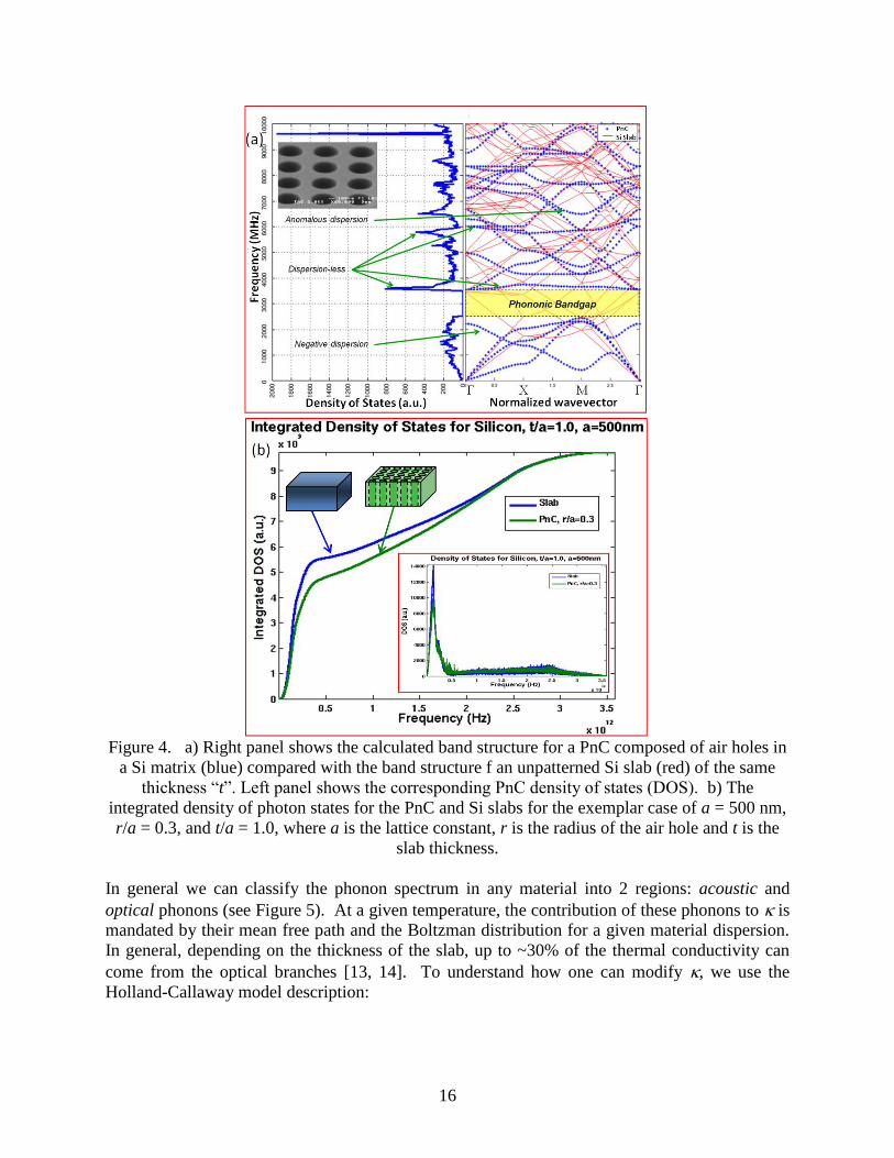
anomalous dispersion spectrum, shown in Figure 4a as compared to the unperturbed bulk
material, results in the creation of dispersion-less (flat) bands where the phonon group velocity
is greatly reduced, in addition to negatively sloping bands (negative group velocities) or
backward propagation of phonons (backscattering).
Figure 3. Phononic crystal concept: a) Schematic of the phonon distribution in a bulk material.
b) Schematic of the phonon distribution in a 2D PnC structure. c) Conceptual visualization of
Bragg and Mie resonance scattering. d) SEM image of a fabricated PnC consisting of a square
array of tungsten rods in a Si membrane; a is the lattice constant, r is the radius of the tungsten
rods, and t is the membrane thickness (not shown in image).
16
Figure 4. a) Right panel shows the calculated band structure for a PnC composed of air holes in
a Si matrix (blue) compared with the band structure f an unpatterned Si slab (red) of the same
thickness ―t‖. Left panel shows the corresponding PnC density of states (DOS). b) The
integrated density of photon states for the PnC and Si slabs for the exemplar case of a = 500 nm,
r/a = 0.3, and t/a = 1.0, where a is the lattice constant, r is the radius of the air hole and t is the
slab thickness.
In general we can classify the phonon spectrum in any material into 2 regions: acoustic and
optical phonons (see Figure 5). At a given temperature, the contribution of these phonons to is
mandated by their mean free path and the Boltzman distribution for a given material dispersion.
In general, depending on the thickness of the slab, up to ~30% of the thermal conductivity can
come from the optical branches [13, 14]. To understand how one can modify , we use the
Holland-Callaway model description:

17
j
qjj
B
j
B
j
B
jdqqqqv
Tk
q
Tk
q
Tk
q22
22
22
2
1exp
exp
6
1
(6)
where is the reduced Planck’s constant, q is the phonon dispersion, Bk is the Boltzmann
constant, T is the phonon temperature, qqqv is the phonon group velocity, qj is
the phonon scattering time, and q is the wavevector. Here, is summed over all phonon modes
―j‖. Assuming only Umklapp and boundary scattering: ,11
,
LqvqqjjUj where
TBqATqjU /exp21
, , A and B are dispersion-fit coefficients, and L is the minimum
distance between sample boundaries (minimum feature size). Thus, in order to modify , we
have to engineer the dispersion (q) or the phonon lifetime (q).
The periodic mechanical impedance mismatch in a PnC [15] results in anomalous dispersion not
found in a homogeneous material. This includes the creation of phononic bandgaps,
dispersionless (low group velocity) bands, and even negative dispersion (negative group velocity
or backward scattering) bands. Figure 4 shows an illustration of these phenomena in a SiC/air
PnC. The result is the complete inhibition of phonon propagation in the bandgap region and
generally a large reduction in the phonon mobility elsewhere. All such phenomena are termed
―coherent scattering‖ and are manifested only in the frequency ranges where the phonon
wavelength is of the same order of the PnC lattice periodicity. Thus, in PnCs with minimum
feature sizes on the order of 250 nm, we predict that these coherent effects will affect acoustic Si
phonons up to the validity of the Debye material limit, i.e., 15 THz for the acoustic longitudinal
phonons and 10 THz for the transverse acoustic ones. However, coherent scattering can also
affect ultra-high frequency phonons in an indirect yet effective manner. This is due to the fact
that 30% of all optical phonon relaxation processes involve an acoustic phonon [16]. Thus by
suppressing the acoustic phonon population we indirectly inhibit the optical phonon relaxation
by up to 30% and hence limit their contribution to thermal conductivity.
Figure 5. Classification of phonon spectrum.

18
In addition to coherent scattering, incoherent boundary scattering events are concurrently present
in the PnC lattice. These are instigated by the simple existence of the scattering centers
irrespective of their arrangement. The dominant factor here is the edge-to-edge separation of the
scattering centers, or minimum feature size L, which caps the phonon lifetime . Incoherent
scattering influences phonons across the high frequency bands, provided that their corresponding
wavelengths are smaller than or on the order of the minimum feature size of the PnC lattice.
This ultimately results in a reduction in the thermal conductivity by as much as 90% [15] with
minimal effects on the electrical conductivity.
Figure 6. Schematic of a TE PnC thermoelectric device.
The overall effect is anticipated to be the doubling of the thermoelectric figure of merit ZT over
that of the underlying material, in this case Si. Given the fact that the PnC technology is portable
to any material set, we anticipate that this factor of 2 enhancement in ZT can be realized in any
material system subject to it lending itself to PnC fabrication and assuming that is phonon
dominated. This result promises to have profound implications for TE technology, and we
anticipate that it may indeed lead to the creation of the next generation of high-ZT TE devices,
such as the schematic shown in Figure 6.
A detailed description of the experimental and theoretical validation of these results is given in
the following sections.

19
2. CALCULATION OF THE THERMAL CONDUCTIVITY OF PHONONIC CRYSTALS
The thermal conductivity of a crystalline solid is directly dependent on the phonon band
structure. Properties such as the phonon group velocity, heat capacity, and phonon scattering
rates can be extracted from the phonon dispersion. The Callaway-Holland method combines
these properties to predict thermal conductivity, and is applicable for materials where the thermal
conductivity is dominated by phonon, rather than electron, transport. The plane wave expansion
(PWE) technique is employed in this work to determine dispersion for various PnC systems, with
the material modeled as a continuum at the macro-scale. This information is incorporated into
the Callaway-Holland model, while also the lattice dynamics (LD) behavior for the host bulk
material is utilized.
2.1. Callaway-Holland Methods
There are two general forms of the Callaway-Holland model for the calculation of the thermal
conductivity from phonon dispersion. The difference lies in whether the dispersion information
is integrated over frequency space (which includes a density of states calculation) or wave vector
space. Both forms require knowledge of the modal velocities, heat capacity, and scattering
lifetimes deduced from the dispersion. One form of this model may be more convenient to
implement over the other depending on variables such as the occurrence of branch crossings in
frequency versus wave vector space and the ease of calculating the phonon density of states of a
given system.
Both forms of the Callaway-Holland originate from the first law of thermodynamics, where
energy is conserved as it is transferred by phonons through the lattice. The Boltzmann transport
equation further defines the problem for crystalline structures by relating the change of phonon
distribution to an applied temperature gradient and wave speed through the medium. The three
factors considered when calculating thermal conductivity κ are: the volumetric specific heat Cp
of the phonons, the group velocity at which the phonons travel through the lattice gv
, and their
rate of scattering τ. Thus, the thermal conductivity can be calculated by integrating these factors
together over the non-dimensional wave vector q and summed for all polarization branches
[17]:
.),(),()ˆ),(( 2
qdqqClqv pg
(7)
In Eq. (7), the phonon heat capacity is expressed per volumetric unit a3 and the phonon velocity
is dotted with the unit vector l along the principle axes. A change of variable from q to k, which
has dimensions of m-1
, is done to incorporate the lattice constant a:
2/akdqd
. (8)
A factor of 2π appears in the formula to account for the volume of the Brillouin zone geometry
of face-centered cubic structures. This enables us to replace Cp with Cph, which is the heat
capacity expressed in units of joules per Kelvin. Now Eq. (7) becomes
kdklkvkC gph
),()ˆ),((),(
)2(
1 2
3 . (9)
20
The material in this case is assumed to be isotropic, allowing for the variable of integration k to
be evaluated over the volume of a sphere and expressed as a scalar, that is
a
dkkkd/2
0
24
. (10)
This is an approximation to the near-spherical shape of the first Brillouin zone. In addition, the
dot product in Eq. (9) for a 3D system or three coordinate directions is reduced to 3-1/2
:
.3
)ˆ),((v
lkvg
(11)
The final form of the Callaway-Holland equation in k-space is expressed for a face-centered
cubic lattice along the Γ-X path (0 to 2π/a) as
a
gph dkkkkvkC/2
0
22
3),(),(),(
)2(
3/4 . (12)
The heat capacity Cph measures the energy of each phonon mode and incorporates the
Boltzmann-Einstein distribution to account for quantum effects at low wavenumbers. Here ω is
the phonon frequency, kB is the Boltzmann constant, ħ is the reduced Plank’s constant, and T is
the temperature:
2
2
1)/),(exp(
)/),(exp(),(),(
Tkk
Tkk
Tk
kkkC
B
B
B
Bph
(13)
The phonon group velocity is calculated by taking the derivative of the phonon frequency with
respect to the wave number:
k
kkvg
),(),(
(14)
Finally, the phonon scattering lifetime can be broken into three major components based on the
Umklapp (τU), impurity (τI), and boundary (τB) scattering processes. The inverse of these
variables are summed according to Matthiessen’s rule, which enables certain terms to be
dominant over the others:
14/2
1111
/),(),(
),(),(),(),(
LckDekAT
kkkk
TB
BIU
(15)
The Umklapp scattering, which models the phonon-phonon interactions, has two fitted
parameters A and B. The impurity scattering (e.g., from the natural defects of the material) are
accommodated by the parameter D. The final term of boundary scattering incorporates surface
interactions, or more generally any interactions with interfaces. The boundary scattering is
dependent on the speed of sound through the material c (more accurately evaluated as ν(k,λ)) and
the minimum feature length L, which is determined by boundaries, grains, or voids introduced
within the material.
We use the relationship between the scalar component of the group velocity and that of the phase
velocity,
,),(
),(k
kkv p
(16)
to change the variable of integration of the Callaway-Holland formulation from wave vector
space to frequency space. This relationship allows us to modify the integrand as

21
d
vvd
d
dk
vdkk
gpp
12
2
2
22 (17)
This expression can be further simplified by introducing the phonon density of states per unit
volume (note that N=ʃ k2dk) defined as [18]:
.),(
1
),(),(
1),(,
2
22
gpg vvvk
d
dk
dk
dN
d
dND (18)
The final form of the Callaway-Holland model in frequency space can thus be written as
0
0
2
2),(),(),(),(
6
1dDvC gph (19)
where υ is the available states (e.g., branch polarizations) across dω. This is the most general
form of the frequency space version of the model; however, due to the difficulty in identifying
the mode type in the phonon dispersion calculations (especially when the band structure is
complex), Eq. (19) is implemented in this work with the following approximation
0
0
2
2),()()()(
6
1
dDvC gph (20)
where Cph(ω) is the heat capacity at a given frequency irrespective of the dispersion branch,
νg(ω) is the group velocity of the bulk material at a given frequency averaged over the first three
branches, τ(ω) is the scattering time constant calculated according to Eq. (15) at a given
frequency irrespective of the dispersion branch and using νg(ω) for the sound velocity, and the
density of states is summed over all dispersion branching prior to integrating.
2.2. Bloch Mode Plane-Wave Expansion Technique
Many methods are available for calculating the transmission and dispersion properties of PnCs,
depending on the behavior being studied; whether time-domain or frequency-domain information
is desired; and what a priori assumptions, if any, can be made. Perhaps the most commonly used
of these techniques are finite-difference time-domain (FDTD), finite element modeling (FEM),
and plane-wave expansion (PWE). In this work, we primarily utilized the FDTD and PWE
methods, with lattice dynamics (LD) used solely for the calculation of the bulk phonon
dispersion of Si. FDTD is useful for simulating structures having finite dimensions (rather than
infinitely periodic) and obtaining transmission and reflection data that can be used to directly
compare with experimental results. However, for revealing phononic bandgaps and calculating
the heat transport properties of PnCs, it is often more appropriate to assume and infinite crystal
and calculate the dispersion behavior of the unperturbed PnC. Thus, PWE was used extensively
in this study, since it provides frequency and spatial profile information about the dispersion of
all elastic modes allowed by the periodicity of the PnC. The technique and its application to
thermal conductivity modeling are described here.
The plane-wave expansion technique [19, 20] operates under the assumption of Bloch’s theorem
for periodic media, which asserts that the elastic wave displacement u(r) can be written in the
following form:
,)( rie k
kuru (21)

22
where r is the position vector, k is wave vector and uk is a periodic function having the same
periodic structure as the materials that make up the PnC. The density ρ(r) and elastic stiffness
tensor C(r) can be written as expressions having corresponding forms. Using Fourier analysis,
the components of the displacement can be expanded as 31,, where, kjieuu tii
j
G
rGkj
G
(22)
where uG is a Fourier coefficient, ω is the angular frequency, t is time, and G is the reciprocal
lattice vector. This Fourier expansion can be substituted into the second-order elastic wave
equation for displacement fields with no body force, written as
,),(
)(),()(,,
lkj l
k
ijkl
i
jx
trurC
xtrur
(23)
where xi is the i-th component of the position vector. After expanding the resulting set of
equations and collecting like terms, an eigenvalue problem can be constructed of size 3N x 3N,
where N is the number of reciprocal lattice vectors (RLVs) used to expand the displacement
field. The eigenvalues of this equation system correlate with the frequencies of each mode at a
given point in k-space; hence the dispersion diagram for a PnC is calculated by finding the
eigenvalues at consecutive points defining the irreducible Brillouin zone (IBZ) of the periodic
lattice. The corresponding eigenvectors contain information about the spatial distribution of the
elastic displacement field, and can be used to reconstruct the displacement field of a given PnC
mode.
While this technique as presented is perfectly suitable for 2D simulations or simulations of 3D
that are periodic in all three dimensions, an adjustment must be made to simulate planar PnC
structures that have a finite thickness in the third dimension. In this case, the supercell method
[21] can be used to account for the finite thickness of the PnC slab. With this modification, the
Fourier structure factor components are calculated for a full 3D structure, where a slab of air is
included above and below the slab to isolate it elastically from the adjacent virtual‖ unit cells in
the vertical direction, as shown schematically in Figure 7. Although RLVs corresponding to the
third dimension are now included, the z-component of the wave vector is zero, since there is not
actual periodicity in that direction. Additionally, several terms in the eigenvalue problem that
dropped out in the 2D case can no longer be neglected, resulting in a significantly more
complicated calculated at each k-point. Note that unlike in Ref. [21], where the Fourier structure
factor components were calculated analytically, the code used for this study used a more
universal fast-Fourier transform (FFT) implementation.

23
Figure 7. Illustration of the computation domain used for the supercell PWE calculation, with air
layers above and below the Si PnC later (red). The actual unit cell used in the simulations is
shown in blue.
A notable improvement to the plane-wave expansion scheme can be implemented in a
straightforward fashion using the reduced Bloch-mode expansion (RBME) technique. This
modification allows for convergence of the calculated dispersion using fewer RLVs by
expanding the displacement field with calculated solutions to the eigenvalue problem at nearby
k-points. Thus, the full 3N x 3N, problem need only be solved the high-symmetry points of the
IBZ, after which those Bloch wave solutions are used in place of the ordinary plane waves to
expand the fields for the intermediate points. This can result in more than an order of magnitude
reduction in the required computation time for calculation of the dispersion diagram of a PnC,
greatly speeding up parametric sweep calculations used to plot the bandgap map of a given PnC
topology. The resulting bandgap map for a finite-thickness PnC composed of cylindrical air
holes in a Si matrix is shown in Figure 8, where complete bandgap formation is observed only
for normalized radii r/a > 0.4 and slab thicknesses between t/a = 0.25 and 2 [22]. The material
properties assumed in the simulation are given in Table 1; notice that non-physical parameters
were used for ―air‖ to ensure stability of the code.

24
Figure 8. Bandgap map versus hole radius for a PnC composed of air holes in Si for various slab
thicknesses.
Table 1. Material parameters used in PWE simulations of Si PnCs
Material Density (kg/m3) C11 (GPa) C12 (GPa) C44 (GPa)
Silicon 2330 217.3 84.5 66.4
Air 10-4
10-3
-10-3
10-3
2.3. Lattice Dynamics Technique
For bulk silicon, we consider a discrete (e.g., an atomic-level) model for which we obtain the
dispersion using LD [23]. We consider a primitive cell consisting of a two-atom basis (with each
having three degrees of freedom) and generate the equations of motion by identifying the
prescribed interactions of each atomic pair. An interatomic energy potential, which can be
obtained empirically, is used to derive the force constant matrix for atoms j and j’. The
equations of motion are thus written as
,);();(
j
j jjujjum (24)
where u denotes displacement, m denotes atomic mass and α and β represent Cartesian
directions. Upon assuming a travelling wave solution,
,),( tiiAetru rk (25)
where A denotes complex displacement amplitude, the following eigenvalue problem is
constructed (under the quasi-harmonic approximation):
0)()()( 2 AID (26)
In Eq. (26), D is the dynamical matrix of size of 3M x 3M, where M represents the number of
atoms considered in the primitive cell. Upon solving Eq. (26) we obtain ω() and A(), which
are the phonon frequencies and polarization vectors, respectively. As in the continuum

25
mechanics method using plane wave expansion, the dispersion is calculated by finding the
eigenvalues at consecutive k-points defining the boundary of the irreducible Brillouin zone
which in this case corresponds to the primitive cell of bulk silicon.
The Tersoff potential [24, 25] is used to model the interatomic forces with second nearest
neighbor interactions considered, allowing for a relaxed Si-Si atomic separation distance of a =
0.38nm. The available degrees-of-freedom for two atoms allow for six branches to be plotted
across the Γ-to-X direction of the primitive cell IBZ with a k-space resolution n set to be greater
than 256. The baseline thermal conductivity of Si was calculated from these data using the above
Callaway-Holland k-space formulation.
2.4. Thermal Conductivity Calculations
Both forms of the Callaway-Holland require knowledge of the modal velocities, which in the
bulk case can be calculated from LD simulations, and the phonon scattering lifetimes, which are
typically parameterized and fit numerically to experimental data. In the PnC case, the modal
velocities cannot be easily calculated due to the complexity of the dispersion diagram, and are
therefore approximated using various methods, as described next.
2.4.1. Density of States Method
Using the DOS formulation, the phononic DOS is calculated by first calculating the dispersion
behavior, not for just the boundary of the IBZ, but for the entire k-space area enclosed in it. The
frequency axis is then divided into bins, and the number of modes lying within each bin is
summed, giving the DOS. Note that it is impossible to separate modes of different types (i.e.
longitudinal, in-plane transverse, or out-of-plane transverse) in this calculation, making direct
calculation of the appropriate velocity for a given mode very difficult and thus necessitating an
approximation of the velocity to be made. The simplest approximation that can be made that still
preserves a measure of accuracy is based on the Debye model [18], which essentially assumes
that dispersion of the bulk material is linear, giving a single velocity for the transverse and
longitudinal modes, respectively. As shown in Figure 9, this approximation gives significant
errors in the velocity of the bulk material on the highly-dispersive frequencies ranges, and in the
case of the transverse modes in the region where there is a mode gap.

26
Figure 9. Phononic dispersion of bulk Si for Γ–Χ (black curves), along with the corresponding
dispersion from the Debye approximation for transverse (red dashed curve) and longitudinal
(blue dashed curve) modes.
Additionally, the PWE technique is also limited by the available computing resources as to how
high in frequency the dispersion behavior can be calculated, since more RLVs are required to
reach higher frequencies. Since the size of the problem is approximately dependent on the
square of the number of RLVs, the computational load requirements quickly become larger than
what can be handled by a supercomputer in a reasonable amount of time. For example, a PWE
dispersion calculation for 20 k-points using 253 RLVs takes about 60 hours to complete on the
Redsky supercomputer at Sandia Labs using 8 processors (8 cores each) and 96 GB of memory.
This hefty calculation yields a maximum frequency of only 3 THz for a PnC having a lattice
constant of 500 nm. Furthermore, the since the results of PWE are known to be inaccurate for at
least the highest half of the frequencies calculated, these values must be thrown out, further
limiting the maximum frequency that can be reached. Therefore, the Callaway-Holland
calculation of thermal conductivity is carried up to the maximum phonon frequency in Si of
about 15 THz by simply supplementing the PWE data with the known bulk dispersion behavior
of Si for frequencies greater than what can be calculated accurately using PWE.
However, the errors introduced by these issues are mitigated by dividing the calculated thermal
conductivity of a given PnC structure by the thermal conductivity of a slab of the same thickness
but having no air holes (r = 0) calculated using the same assumptions. In this way, the errors due
to approximation, which should be roughly the same in the two calculations, can be canceled out,
resulting in a reasonable estimation of the thermal conductivity of the sample relative to an
unpatterned slab. Given that the thermal conductivity of a slab can be calculated relative to a
bulk material of known thermal conductivity, the reduction in thermal conductivity of a PnC
relative to bulk (as well as the absolute value) can be extracted as well.
This method was used to calculate the thermal conductivity reduction of a set of PnC samples
fabricated in Mesa facilities at Sandia Labs, composed of 500 nm thick Si with a square lattice of

27
air holes with lattice constants ranging from 500 to 800 nm and hole radii from 150 to 200 nm
[26]. The results of the simulations are shown in Figure 10, along with a model of the thermal
conductivity of an unpatterned slab and measured data from three other published results. For
the thermal conductivity predictions, the velocities used in the Callaway-Holland model were a
weighted combination of the Debye velocities for the Γ–Χ direction in Si, assuming that there
are two transverse modes for each longitudinal one. The measured thermal conductivities of the
porous structures are multiplied by a factor of (1 + 2ff/3)/(1 - ff) (where ff is the filing fraction) to
account for the porosity of the structures, and thereby directly compare the thermal conductivity
of the solid matrix in the porous structures to the model of the unpatterned slab. Clearly, Figure
10 demonstrates that the calculated thermal conductivity ratios agree well with the experimental
data measured using the TDTR technique described in Section 4.2.
Figure 10. The thermal conductivity of Si structures at room temperature as a function of L for
the PnCs (unfilled squares), microporous solids (filled pentagons), nanomesh (filled diamond),
and a suspended 500 nm thick Si films that is, an unpatterned Si slab (unfilled circle). The
references are from [26]. The solid line represents predictions of the unpatterned slab at room
temperature as a function of L. The dashed line represents predictions of the PnC thermal
conductivity using DOS data from PWE calculations.
2.4.2. DOS with Slab Padding
Since the PWE method only account for porosity and coherent scattering (not incoherent
scattering), it is reasonable to expect that the dispersion behavior of a PnC slab should gradually
approach that of an unpatterned slab as frequency increases due to the shorter wavelength
phonons no longer ―seeing‖ the periodic lattice of ―large‖ inclusions but rather a bulk effective
medium. This is confirmed by plotting the integrated DOS for both a given PnC and its
corresponding slab. As seen in Figure 11, the difference between the two curves becomes
negligible after a point, indicating that the behavior of the two structures from the thermal
conductivity point of view is equivalent. Moreover, since the PWE simulations are performed
using normalized parameters (i.e. frequency scales inversely with lattice constant) and an

28
unpatterned slab has no in-plane variation with lattice constant, the data from the slab
simulations can be rescaled to reach higher frequencies. In other words, assuming that the slab
thickness does not change, a slab having a normalized thickness t/a = 1 has similar dispersive
behavior to a slab of thickness t/a = 10, but with a lattice constant that is 10 times smaller
(resulting in frequencies that are 10 times higher). Thus, the PnC DOS data can be ―padded‖
with slab data for frequencies greater than this point, eliminating some of the error in
approximating the structure as bulk for frequencies greater than what can be reached with PWE.
Figure 11. Integrated DOS for a Si slab of 500 nm thickness and a PnC of the same thickness
and with 150 nm radius air holes.
2.4.3. Dispersion Method with Mode Velocities
In an effort to further improve the accuracy of the PWE calculations, particularly at higher
frequencies, a scheme was developed to account for the dispersive behavior of bulk Si in the
Callaway-Holland model. The theory behind this scheme is that the dispersion of Si can be
approximately accounted for in PWE, which assumes that the material parameters are constant
with respect to frequency (i.e. dispersionless), by calculating an effective mode velocity at each
point in the dispersion diagram based on the actual modal velocities of the bulk material. The
underlying assumption in this method is that the dispersive effects of the PnC act as a
perturbation of the bulk dispersion in the vicinity of the corresponding frequency. Thus, the
velocity of a given mode at a point in the dispersion can be approximated as a weighted average
of the two modal velocities of the bulk material at that frequency, given by
222
22222
zyx
TyxLz
PWEuuu
vuuvuv
(27)
where vPWE is the velocity of a mode at frequency ω calculated using PWE; ux, uy, and uz are the
x, y, and z components of the displacement, respectively; vL is the longitudal mode velocity of the
bulk material at frequency ω, and vT is the transverse mode velocity of the bulk material at

29
frequency ω. The mode velocities of the bulk material are calculated from the dispersion from
the LD technique. Using this approach, the linear dispersion approximation from the Debye
model is removed, and even though transverse modes at frequencies in the mode gap will
incorrectly appear in the PWE calculations, they will be assigned zero velocity, thus eliminating
them from consideration in the Callaway-Holland calculation.
2.4.4. Multi-Scale Method
A final improvement to the inherent approximations in the PWE technique involves combining
the dispersion calculated from PWE for a PnC with the PWE dispersion for a slab of the same
thickness and LD dispersion for the bulk material in a strategic manner to capture the effects of
the PnC on thermal conductivity as accurately and efficiently as possible. Using this multiscale
approach, dispersion from PWE is used at lower frequencies, where the PnC has the greatest
effect on phonon propagation, and is padded with the dispersion from LD for the bulk material at
higher frequencies, where PWE calculation become inaccurate or intractable. Since the PnC will
still be padded with data for the slab of corresponding thickness, as described above in Section
5.2.2, there are now two adjustable parameters in the frequency domain: the upper frequency for
which the PWE dispersion is accurate and is distinguishable from the slab DOS, and the upper
frequency for which the Debye approximation is still accurate and thus the re-scaled PWE
dispersion for the unpatterned slab can still be used. The former frequency, fPnC, is
approximately 1 THz, and the latter frequency, fslab, is approximately 2.5 THz (lower of the
Debye limits for the transverse and longitudinal modes), as shown schematically in Figure 9.
The parameters must be ―tuned‖ to best fit experimental data, and generally vary slightly
depending on the dimensions of the PnC under consideration.

30

31
3. FABRICATION OF PHONONIC CRYSTAL DEVICES
To validate our theoretical predictions above, we needed to fabricate phononic crystal samples
with a high degree of fidelity and yield. Below is a description of the two methods that were
used as venues for achieving the desired structural values.
3.1. MESA Silicon-Fab
The Microsystems & Engineering Sciences Applications (MESA) Complex at Sandia National
Laboratories represents the essential facilities and equipment to design, develop, manufacture,
integrate, and qualify microsystems for the nation’s national security needs that cannot or should
not be made in industry—either because the low volumes required for these applications are not
profitable for the private sector or because of stringent security requirements for high-
consequence systems such as nuclear warheads. Microsystems extend the information
processing of silicon integrated circuits to add functions such as sensing, actuation, and
communication—all integrated within a single package. The MESA Complex integrates the
numerous scientific, engineering, and computational disciplines necessary to produce functional,
robust, integrated microsystems at the center of Sandia’s investment in microsystems research,
development, and prototyping activities.
The designed test structures, shown in Figure 12, were fabricated in Sandia MESA facility.
Figure 13 shows the schematics of the thermal conductivity test structure fabrication process.
The fabrication starts with 6-inch silicon-on-insulator (SOI) wafers. The device layer is 500 nm-
thick lightly p-type doped (boron, concentration 1016
/cm3) single crystal silicon. On top of the
SOI wafers, 100 nm of undoped amorphous silicon was blanket deposited as an electrical
isolation layer between the underlying device layer and the following metal contact layer (Figure
13a). High temperature annealing was used to relax the high stress in the amorphous silicon
layer. Then, aluminum was deposited and patterned to form heaters, temperature sensors,
interconnects, and bondpads (Figure 13b). Using plasma etching, phononic crystals and release
trenches were defined in the silicon layers (Figure 13c). As the final step, the buried oxide
(SiO2) underneath the test structure was removed by a timed HF vapor etch to release the bridge
(Figure 13d). Figure 14 shows scanning electron microscope (SEM) images of a fabricated
thermal conductivity test structure.

32
Figure 12. A schematic of the thermal conductivity test structure design. A phononic crystal bridge is
suspended from the substrate. Serpentine aluminum traces are installed at both the bridge center and
both bridge ends. While heat is supplied at the center, the temperature gradient across the bridge is
measured to extract device thermal characteristics.
Figure 13. Schematics of the fabrication process for the thermal conductivity measurement
structures.
Phononic CrystalsSerpentine
Heater/Sensor
Temperature Sensor
Temperature Sensor
Substrate Substrate

33
Figure 14. SEM images of fabricated simple cubic (SC) phononic crystal thermal conductivity
test devices.
3.2. Focused Ion Beam
This section describes how PnCs were fabricated with a tool called a focused ion beam, or FIB.
All of the FIB milling and nanoFIBrication in this work was performed on a dual-beam Quanta
3D FEG made by the FEI Corporation. The dual-beam refers to the system having both a FIB
and an SEM.
A FIB is a system that generates a focused stream of charged particles (ions). Ions are extracted
from a material, accelerated, and then focused into a narrow beam with a Gaussian density
distribution using various apertures and electro-magnetic fields in an octopole arrangement.
Figure 15 shows a schematic of the basic components in a FIB.
Figure 15. Schematic of a focused ion beam (FIB) system. Ions are extracted and then focused
by multiple apertures and electromagnetic fields onto a sample. All of the FIB components and
sample are under vacuum to prevent degradation. (Image courtesy of FEI)
Heater/Sensor
Temperature Sensor
Suspended SC- Silicon Phononic Crystal Bridge
Temperature Sensor
10um
Diameter
Hole Pitch (Lattice constant)
Limiting Dimension

34
A common source for generating ions is called a liquid metal ion source (LMIS) [27]. Figure 16
shows a drawing of a LMIS. Liquid metal from a reservoir is allowed to flow onto the tip of a
sharp needle. The most common metal used is gallium due to its low melting point, low vapor
pressure, and low reactivity with other elements, along with the fact that it produces mainly
singly charged ions and it has enough mass to dislodge material at an acceptable rate [28]. As
the liquid metal rests at the tip of the needle, an extractor lens with a large accelerating voltage
pulls positively charged ions from the liquid. Typical accelerating voltages are between 5 and 30
kV.
Figure 16. Drawing of a liquid metal ion source. Liquid metal wets a sharp tip and an extractor
lens extracts ions from the metal by using a high accelerating voltage in the kV range.
Once the focused beam of ions leave the ion column, they interact with the sample surface.
When a single Ga+ ion strikes the sample surface, it can have enough energy and momentum to
cause other atoms at the sample surface be removed, or sputtered away. The mean number of
atoms removed for a single ion striking the sample surface is known as the sputter rate of the
material, which is a dependent on the type of ion bombarding the surface, the accelerating
voltage of the ion, and the angle of incidence. Increasing the accelerating voltage increases the
sputter rate. As the angle of incidence changes from 0 to approximately 80° (with respect to
normal), the sputter rate increases then quickly drops from 80° to 90°. A plot of sputter rate
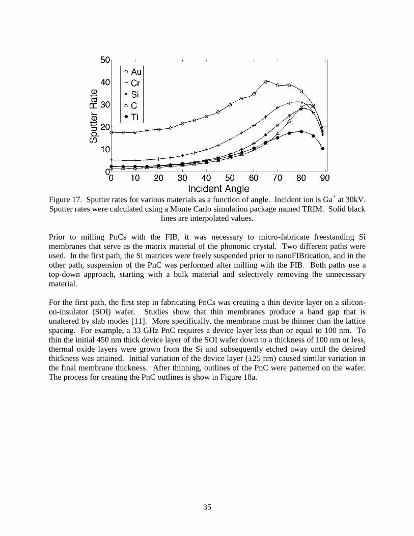
versus angle for various materials is shown in Figure 17. The ion species is Ga+ at 30 kV.
Sputter rates were calculated using a Monte Carlo simulation package named TRIM (Transport
of Ions in Matter). TRIM calculates the stopping and range of ions into matter using a quantum
mechanical treatment of ion-atom collisions [29]. The solid lines in Figure 17 are interpolated
values.
35
Figure 17. Sputter rates for various materials as a function of angle. Incident ion is Ga
+ at 30kV.
Sputter rates were calculated using a Monte Carlo simulation package named TRIM. Solid black
lines are interpolated values.
Prior to milling PnCs with the FIB, it was necessary to micro-fabricate freestanding Si
membranes that serve as the matrix material of the phononic crystal. Two different paths were
used. In the first path, the Si matrices were freely suspended prior to nanoFIBrication, and in the
other path, suspension of the PnC was performed after milling with the FIB. Both paths use a
top-down approach, starting with a bulk material and selectively removing the unnecessary
material.
For the first path, the first step in fabricating PnCs was creating a thin device layer on a silicon-
on-insulator (SOI) wafer. Studies show that thin membranes produce a band gap that is
unaltered by slab modes [11]. More specifically, the membrane must be thinner than the lattice
spacing. For example, a 33 GHz PnC requires a device layer less than or equal to 100 nm. To
thin the initial 450 nm thick device layer of the SOI wafer down to a thickness of 100 nm or less,
thermal oxide layers were grown from the Si and subsequently etched away until the desired
thickness was attained. Initial variation of the device layer (±25 nm) caused similar variation in
the final membrane thickness. After thinning, outlines of the PnC were patterned on the wafer.
The process for creating the PnC outlines is show in Figure 18a.

36
Figure 18. Fabrication process for creating a thin-freestanding membrane for PnCs. a) Cross
sectional view of fabrication process. b) Released freestanding membrane.
The second method for fabricating Si matrices is similar to the first method, but the release step
is performed after milling with the FIB. The process flow is shown in Figure 19.
Figure 19. Second fabrication method for creating a thin-freestanding PnC. a) Cross sectional
view of fabrication process. b) Released freestanding PnC.
In both methods, a protective layer is placed on top of the Si. The protective layer minimizes
Ga+ doping in the Si layer, which can affect both the electrical [30] and thermal properties [31]
of Si. Since the goal of this effort is to determine how a PnC affects the thermal conductivity of

37
Si, it is important to minimize any additional variables that could affect the thermal properties of
Si.
The choice of the proper protective layer is dependent on a number of factors. It must be
relatively easy to add and remove. The protective layer needs to be compatible with the
fabrication process. It must also be relatively thin. If it is too thick, then the ion beam will have
a difficult time penetrating both the protective layer and the Si. Another consideration is
electrical conductivity. If it is not conductive, then the incoming charged ions will be affected.
As charge builds up on the sample surface, the ion beam will become distorted and will no
longer mill the desired area. Last, it should have a sputter rate that is less than that of Si.
The best types of materials to be used as a protective layer are metals. Metals make a good
protective layer for multiple reasons. They are easy to deposit, it is easy to find an etchant with a
high selectivity between a given metal and Si, they are highly conductive which improves
imaging in the SEM, and only a thin layer is required to block Ga+ ions from penetrating into Si.
For example, TRIM calculations of Ni show that 30 kV Ga+ ions have a mean penetration depth
of 9.7 nm into a 100 nm thick layer of Ni, and only a small percentage reach beyond 30 nm
(Figure 20). Unfortunately, Ni reacts with the fluorine in a hydrofluoric acid vapor and leaves a
thin, greenish layer of NiF2 on the PnC. Ti has a mean penetration depth of 17.9 nm, which is
greater than Ni, but Ti has the advantage of being etched by hydrofluoric acid. Since
hydrofluoric acid is required for removing the BOX layer and thus releasing the PnC, Ti makes a
good choice for a protective layer. To ensure no Ga+ reaches the Si, a 50 nm thick layer of Ti is
used as the protective layer for fabricating PnCs with the FIB.
Figure 20. 30kV Ga+ ion penetration into 50 nm thick layer of Ni on top of 50 nm layer of Si.
No ions reach the Si layer.

38
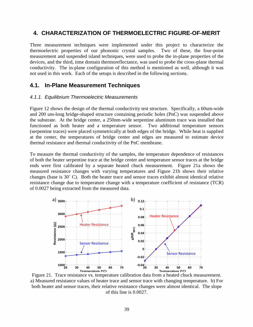
39
4. CHARACTERIZATION OF THERMOELECTRIC FIGURE-OF-MERIT
Three measurement techniques were implemented under this project to characterize the
thermoelectric properties of our phononic crystal samples. Two of these, the four-point
measurement and suspended island techniques, were used to probe the in-plane properties of the
devices, and the third, time domain thermoreflectance, was used to probe the cross-plane thermal
conductivity. The in-plane configuration of this method is mentioned as well, although it was
not used in this work. Each of the setups is described in the following sections.
4.1. In-Plane Measurement Techniques
4.1.1. Equilibrium Thermoelectric Measurements
Figure 12 shows the design of the thermal conductivity test structure. Specifically, a 60um-wide
and 200 um-long bridge-shaped structure containing periodic holes (PnC) was suspended above
the substrate. At the bridge center, a 250nm-wide serpentine aluminum trace was installed that
functioned as both heater and a temperature sensor. Two additional temperature sensors
(serpentine traces) were placed symmetrically at both edges of the bridge. While heat is supplied
at the center, the temperatures of bridge center and edges are measured to estimate device
thermal resistance and thermal conductivity of the PnC membrane.
To measure the thermal conductivity of the samples, the temperature dependence of resistances
of both the heater serpentine trace at the bridge center and temperature sensor traces at the bridge
ends were first calibrated by a separate heated chuck measurement. Figure 21a shows the
measured resistance changes with varying temperatures and Figure 21b shows their relative
changes (base is 30˚ C). Both the heater trace and sensor traces exhibit almost identical relative
resistance change due to temperature change with a temperature coefficient of resistance (TCR)
of 0.0027 being extracted from the measured data.
Figure 21. Trace resistance vs. temperature calibration data from a heated chuck measurement.
a) Measured resistance values of heater trace and sensor trace with changing temperature. b) For
both heater and sensor traces, their relative resistance changes were almost identical. The slope
of this line is 0.0027.
20 30 40 50 60 701000
1500
2000
2500
3000
3500
Temperature (C)
Resis
tan
ce (
)
20 30 40 50 60 70-0.04
-0.02
0
0.02
0.04
0.06
0.08
0.1
0.12
Temperature (C)
R
/R30C
20 30 40 50 60 701000
1500
2000
2500
3000
3500
Temperature (C)
Resis
tan
ce (
)
20 30 40 50 60 70-0.04
-0.02
0
0.02
0.04
0.06
0.08
0.1
0.12
Temperature (C)
R
/R30C
a) b)
Heater Resistance
Sensor Resistance
Heater Resistance
Sensor Resistance

40
Figure 22 shows the thermal resistance measurement setup diagram. Heat is supplied at the
center of the test structure by applying power across the serpentine heater. By measuring the
voltage across the heater and the current through it, both the supplied heat and resistance change
can be simultaneously monitored. At the same time, the resistance change of the sensor traces at
the bridge ends is also measured. Using the above TCR of 0.0027 (from Figure 21), the
temperature changes of the heater and sensors are calculated. All measurements were conducted
in vacuum (< 1 mTorr) while sweeping the heating power from 0 to 1 mW and back to 0 mW
again. Figure 23 shows an example plot of the measured temperature vs. heating power. For
each design set (hole pitch and diameter combination), 6 devices were tested.
Figure 22. Test setup diagram for thermal conductivity measurement.
Figure 23. An example plot of measured temperature vs. heating power plot (Device ID-7).
Temperature difference across the phononic crystal bridge was measured using calibrated
serpentine traces while heating power supplied at the bridge center was sweeping between 0 to 1
mW.
From the measured temperature changes vs. heating power data, the thermal conductivities were
extracted using ANSYS Finite Element simulation models and equivalent thermal circuit models,
as shown in Figure 24. Since all measurements took place in vacuum, convectional heat leakage
can be ignored. Also, radiative heat transfer was estimated to not exceed a maximum of 0.4% of
the conductive heat transfer, and therefore was ignored as well in these models.
V Ω
I
0 0.2 0.4 0.6 0.8 10
5
10
15
20
Power(mW)
T
ab
ov
e R
oo
m T
em
pe
ratu
re(C
)
Heater Temperature
Sensor Temperature
ΔT, Temperature Difference

41
Figure 24. a) ANSYS FEM simulation model and b) equivalent thermal circuit model of thermal
conductivity test structures.
The amount of other parasitic thermal resistance (mostly through the traces connecting the
heaters and bondpads across the bridge) in these models of Figure 24 were verified by measuring
the thermal characteristics of specially prepared samples, of which the phononic crystal regions
were cut out using focused ion beam milling. After accounting for these parasitics, the thermal
resistances only across the phononic crystal regions were extracted and by multiplying with the
cross section areas and dividing with the length, the phononic crystal thermal conductivities were
calculated. Figure 25 shows an example plot of extracted thermal conductivity versus
temperature. As can be seen, at low heating power, the current measurement is too noisy and it
was not easy to obtain reliable and repeatable data. Therefore, for reliability, we used thermal
conductivity values when the average temperature across the bridge is 7˚ C above room
temperature (300 K).
a)
b)Tsensor
Theater Tsensor
Qheat
Qheat/2Qheat/2
T
QR heat
specimen
2 SpecimenRL
Ak
↑
Rspecimen
Rtrace
Rtrace
Rspecimen
Rtrace
Rtrace
Rsensor-substrate Rsensor-substrate
cross-section area
length
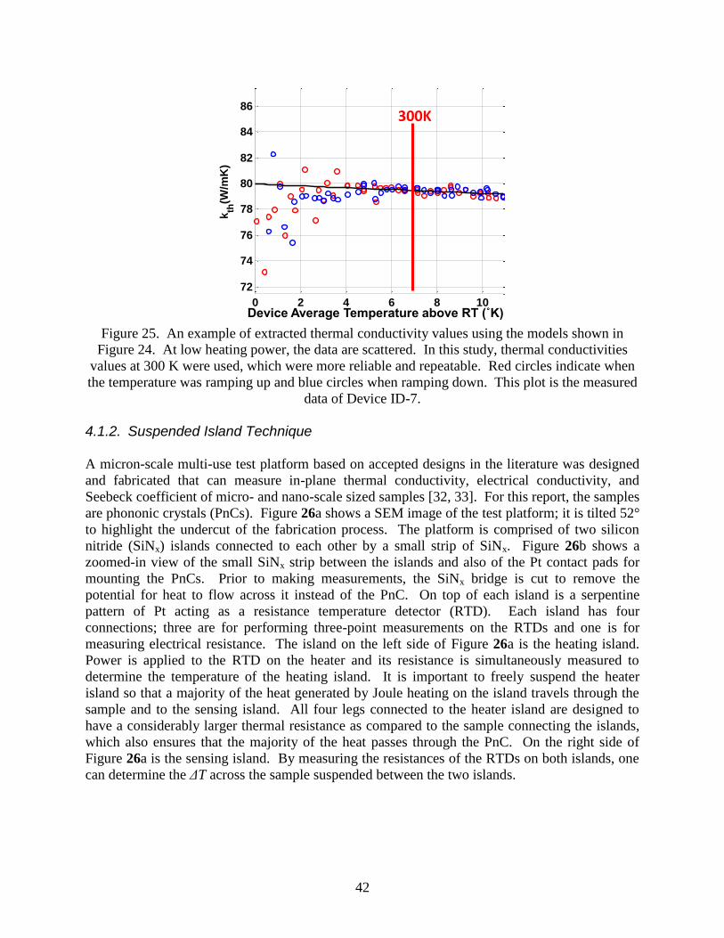
42
Figure 25. An example of extracted thermal conductivity values using the models shown in
Figure 24. At low heating power, the data are scattered. In this study, thermal conductivities
values at 300 K were used, which were more reliable and repeatable. Red circles indicate when
the temperature was ramping up and blue circles when ramping down. This plot is the measured
data of Device ID-7.
4.1.2. Suspended Island Technique
A micron-scale multi-use test platform based on accepted designs in the literature was designed
and fabricated that can measure in-plane thermal conductivity, electrical conductivity, and
Seebeck coefficient of micro- and nano-scale sized samples [32, 33]. For this report, the samples
are phononic crystals (PnCs). Figure 26a shows a SEM image of the test platform; it is tilted 52°
to highlight the undercut of the fabrication process. The platform is comprised of two silicon
nitride (SiNx) islands connected to each other by a small strip of SiNx. Figure 26b shows a
zoomed-in view of the small SiNx strip between the islands and also of the Pt contact pads for
mounting the PnCs. Prior to making measurements, the SiNx bridge is cut to remove the
potential for heat to flow across it instead of the PnC. On top of each island is a serpentine
pattern of Pt acting as a resistance temperature detector (RTD). Each island has four
connections; three are for performing three-point measurements on the RTDs and one is for
measuring electrical resistance. The island on the left side of Figure 26a is the heating island.
Power is applied to the RTD on the heater and its resistance is simultaneously measured to
determine the temperature of the heating island. It is important to freely suspend the heater
island so that a majority of the heat generated by Joule heating on the island travels through the
sample and to the sensing island. All four legs connected to the heater island are designed to
have a considerably larger thermal resistance as compared to the sample connecting the islands,
which also ensures that the majority of the heat passes through the PnC. On the right side of
Figure 26a is the sensing island. By measuring the resistances of the RTDs on both islands, one
can determine the ΔT across the sample suspended between the two islands.
0 2 4 6 8 10
72
74
76
78
80
82
84
86
T above Room Temperature(C)
kth
(W/m
K)
Device Average Temperature above RT (˚K)
300K

43
Figure 26. SEM images of multi-use test platform for measuring thermal conductivity of
phononic crystals. Both images are tilted 52° with respect to normal. a. Overview of suspended
islands. b. Zoom-in of the SiNx bridge connecting the heater and sensing islands. Pt pads on
either side of the bridge provide a location for the PnCs to be welded on to the islands.
Figure 27. Process flow for fabrication of in-plane thermal conductivity test platform.
All of the platforms were fabricated using standard microfabrication techniques; see Figure 27.
First a Si wafer with a 1 µm thick LPCVD SiNx film is spin coated by 1.4 µm thick positive
photoresist (PR). Consequently, 80 nm of platinum is deposited on the wafers by thermal
evaporation. Afterwards, 2 µm thick positive PR is patterned on the wafers to protect the
devices during (reactive ion etching). The SiNx pattern is cut by RIE inside an atmosphere of

44
98% CF4 and 2% O2 plasma. Finally, the silicon underneath the devices is removed with a dry
etch of XeF2 at a pressure of 1 T.
Fabrication of the phononic crystals was undertaken using a focused ion beam technique
developed as a result of this project. Two different phononic crystals comprised of air inclusions
in a Si matrix were tested on the multi-use platform. Both used the same lattice spacing and r/a
ratio. Each PnC had a lattice constant of 250 nm and a radius of 41 nm, which corresponds to an
r/a ratio of 0.16 and critical length of 168 nm. The thickness of the Si was 250 nm (250 nm thick
device layer on a SOI wafer), so the critical length is dominated by the spacing between
inclusions. The difference between the PnCs is the lattice type; one used a simple cubic lattice
and the other used a hexagonal lattice. Figure 28 shows SEM images of the PnCs. The
measured radius for the simple cubic PnC was 41.5 nm ± 2 nm and the hexagonal PnC had a
measured radius of 41 nm ± 2 nm.
Figure 28. SEM images of PnCs measured with multi-use platform. a. Simple cubic PnC. b.
Hexagonal PnC.
Both PnCs were fabricated with a focused ion beam, or FIB. The FIB for this work is FEI’s
Quanta 3D FEG dual beam system, which has both a FIB and SEM. The electron beam is
mounted vertically, and the ion column is mounted 52° from vertical. The beam profile of the
FIB has a Gaussian density distribution of Ga+ ions, and it can be as small as 7 nm at full-width-
half-maximum (FWHM). The accelerating voltage of the Ga+ ions is 30 kV. For the devices
fabricated in this work, a 50 nm protective layer of Ti was deposited on the device layer of the
SOI wafer. By using a protective layer, surface damage by Ga+ ions is confined to the Ti and
does not reach the surface of the thin Si membrane between each via [34]. Protection of the Si
surface also minimizes the possibility of Ga doping affecting the thermal conductivity. Once the
vias are milled, the samples are dipped in 6:1 buffered oxide etch (BOE), which etches both Ti
and the 2 µm thick BOX layer. Next, the samples are dried with a CO2 critical dryer to prevent
stiction failure. For more details about this process see Section 3.2 of this Report.
Since the PnC is not integrated into the test platform, it must be transferred on to the gap
between the islands of the platform. The transfer process makes use of the dual beam FIB/SEM
system that is also equipped with an Omniprobe™ and a Pt gas injection system. The

45
Omniprobe is equipped with a fine tipped W needle with high precision translation movements.
A Pt gas injection system allows Pt to be deposited at user defined location and depth. First, a
protective mask is milled which will be placed on top of the PnC during the transfer process.
This is done to limit Ga doping of the PnC during the transfer to the test platform. Two tabs are
left to suspend the protective layer so the Omniprobe can be attached. After cutting out the
mask, it is welded to the tip of the Omniprobe with Pt and the tabs are then cut to fully release
the mask. Next, the PnC is cut from its resting place. Again, two tabs are left to suspend the
PnC so the mask can be placed on top. Once the protective layer is on top the PnC, it is welded
to the PnC. Next, the tabs are cut and the PnC is transferred to the gap between the test
platforms. With both ends of the PnC touching the Pt pads on the heater and sensing island, a
thin strip of Pt is used to connect the PnC to the Pt pads. Last, the protective layer attached to
the Omniprobe is removed. A picture of mounted PnC on a platform is shown in Figure 29.
Figure 29. PnC mounted onto a thermal conductivity platform.
A thermal circuit of the test platform is shown in Figure 30. Heat generated by the heating island
is labeled QH. QL refers to the heat that passes through a single suspended leg connected to the
heating island, and QS is the heat that passes through the PnC and sensing island. TH is the
temperature of the heating island, TS is the temperature of the sensing island, and TA is the
ambient temperature.
PnCCC
Heater Island
Sensor Island
Pt Welds

46
Figure 30. Electrical and Thermal Circuit of test platform.
The starting point for determining the thermal conductivity is straightforward; heat in equal heat
out:
.4 LSH QQQ (28)
Heat loss through each leg is given by
,Th
L
Th
L
AHL
R
T
R
TTQ
(29)
where Th
LR is the thermal resistance of a single suspended leg. Heat loss across the PnC is given
by
,TL
A
R
TT
R
TTQ
PnC
PnC
PnCTh
PnC
AH
Th
PnC
SH
S
(30)
where Th
PnCR is the thermal resistance of the PnC. Because the sensing island does not have free
standing legs, the boundary condition of the constant ambient temperature is right beside the
island instead and so the temperature of the sensing island is assume to be almost equal to
ambient. Combining Equations 28 through 30 gives
.4
TL
A
R
TQ
PnC
PnC
PnCTh
L
H
(31)
The relationship between resistance and temperature is given by
,TRRR oo (32)
where R is the electrical resistance of the RTD at a given temperature, Ro is the electrical
resistance of the RTD at the initial temperature, and α is the temperature coefficient of resistance.
Substituting Eq. (32) into Eq. (31) gives
,4
o
o
Th
LPnC
PnC
PnCHR
RR
RL
AQ
(33)
where κPnC is the thermal conductivity of the phononic crystal, and APnC and LPnC are the cross-
sectional area and length of the PnC respectively. By rearranging the terms in Eq. (33), a point-
slope equation is reached
,144
Th
LPnC
PnC
PnC
o
Th
LPnC
PnC
PnCHRL
A
R
R
RL
AQ
(34)
Heat Sink @ TA
QH
TH TS
QS
4QL

47
with R as the independent variable and a slope, m, given by
.14
o
Th
LPnC
PnC
PnCRRL
Am
(35)
If the thermal resistance of a single suspended leg is large compared to the thermal resistance of
the PnC, then the second term in the bracket of Eq. (35) can be neglected. For a 100 µm long
suspended leg, the thermal resistance is estimated to be 12 MK/W. If the PnC has a thermal
conductivity near 10 W/m-K, a thickness of 250 nm, width of 6 µm, and length of 17 µm, then
its thermal resistance is less than one-tenth of the leg. Neglecting the second term, the thermal
conductivity of the PnC is given by
.PnC
oPnC
PnCA
RmL
(36)
All of the PnC dimensions are measured with the SEM. The α-term is determined by calibrating
the platform. Ro is measured during testing, and the slope m, is derived from the plot of input
heat versus heater resistance. From these values and measurements, the thermal conductivity of
the PnC can be calculated.
4.2. Cross-Plane Thermal Conductivity Measurement
4.1.2. Time Domain Thermoreflectance Technique
Pump-probe transient thermoreflectance techniques utilizing short pulsed lasers have been
extensively used to measure thermal conductivity, , and thermal boundary conductance, hK, of
nanomaterials and interfaces of nanomaterials, such as in metal films [35], dielectric films
[36], phase change materials [37], thermally anisotropic materials [38], superlattice structures
[39], and layered nanolaminates [40, 41] and hK across metal-metal [42] metal-dielectric [43-47]
and metal-liquid [48] interfaces. These transient thermoreflectance techniques measure the
change in reflectance of the surface of a material as a function of time after a short pulsed
heating event. The change in reflectance is related to the temperature change of the electrons in
the material, and the measured change in temperature as a function of time is then related to
and hK through a conduction heat equation. This experiment is referred to as time domain
thermoreflectance (TDTR).
4.2.1. Cross-Plane TDTR
The experiments and analyses in this LDRD are focused on pulsed laser heating from a
Ti:sapphire oscillator with a fundamental output of 90 fs pulses at 80 MHz (12.5 ns between
laser pulses); the laser pulses are then further modulated at with an electro-optic modulator to
create a modulated heating event at the sample surface, and the temperature decay on the surface
of the samples from this modulated heating events are monitored over ~4 - 8 ns. The laser pulses
are treated as delta functions in time due to the ultrashort pulse width compared to the time delay
of the experiments. The thermal penetration depth of the modulated heat source is estimated by
fD , where D is the diffusivity and f is the modulation frequency. For most solids
subjected to MHz thermal modulation rates, the thermal penetration depth is anywhere from 100
nm – 10 m. To ensure mostly cross plane (one dimensional) transport, the laser spot size of the

48
modulated heating source should be greater than the thermal penetration depth. Typical TDTR
experiments utilize pump spot sizes on the order of 10 m. Therefore, for low diffusivity
systems, the thermal transport measured in TDTR experiments is nearly entirely cross-plane due
to the small thermal penetration depth.
In typical TDTR experiments, the pump and probe beams have spatially Gaussian intensity
distributions when incident on the film surface. Therefore, depending on the relative sizes and
overlap of the beams, the radial distributions of the pump beam could affect the temperature
measured by the probe beam. In this case, the assumption a one dimensional heat transfer model
may not be applicable since it assumes that the probe reflectance, or the measured change in
temperature, is measuring a uniformly heated plane at the surface of the film. To correct for this,
Cahill [49] derived an expression for (r), the temperature rise at the surface of the film,
assuming radial spreading in a half-sphere from the pump pulse. This begins by considering the
axially symmetric heat equation in cylindrical coordinates is given by
r
tzrr
rrz
tzr
t
tzrC
r
z
,,,,,, 1,1
2
1
2
,11
1
, (37)
where r is the radial coordinate, the subscript r and z denote the radial and cross plane
conductivities, and C is the volumetric heat capacity. Taking the Hankel transform along the
radial, planar dimension, then applying a Fourier transform, Eq. (37) leads to
,,,,
1
2
1,2
1
2
zrqz
zrT
, (38)
where is the angular frequency of the pump pulses and
z
rT
iCKq
22 , (39)
where K is the transform variable. This anisotropic q was used by Schmidt et al. [38] to
determine the directionally dependent thermal conductivities of graphite in anisotropic
structures. In this work, however, we consider isotropic materials and we are only interested in
cross plane properties, so iCKqT 22.
The temperature change on the surface of the film due to heat flow through underlying materials
is easily taken into account through Carslaw and Jaeger’s solution for steady periodic
temperature change in composite slabs [50]. A convenient implementation of this is presented
by Feldman [51] and discussed here. The change in surface temperature of material 1 is given by
11
11
1
1
TT
TT
FF
FFkF
, (40)
where
1TF and
1TF are temperature change coefficients related to the forward and backward
propagating waves on the surface (top side) of material 1 and where = qT. The forward and
backward propagating wave at the top side of material 1 are related to the waves on the bottom
side through
1
1
11
11
1
1
exp0
0exp
B
B
T
T
F
F
dq
dq
F
F, (41)

49
where d is the material thickness. For material 1, the top side is assumed at the slab/air interface
and the bottom side is assumed as the interface between material 1 and material 2 (i.e.,
film/substrate). Given a thermal boundary conductance, hK, between material 1 and material 2,
the temperature at the top of slab 2 is related to the temperature at the bottom side of slab 1 by
2
2
12,K
2
1
2
12,K
2
1
2
12,K
2
1
2
12,K
2
1
2
1
1
11
11
2
1
T
T
B
B
F
F
hh
hh
F
F
. (42)
Assuming a bulk substrate, heat cannot reach the bottom side of slab 2 at rates comparable to the
modulation frequency (semi-infinite), so there is no thermal buildup of waves and
222
2
exp
0
dqF
F
T
T . (43)
with Eqs. (40) – (42), this approach gives a straight forward method to solve for heat conduction
through several materials and interfaces via successive implementation of Eqs. (41) and (42) for
each layer and then Eq. (43) for the final, semi-infinite layer. This is much less computationally
expensive than solving the heat equation in the time domain for each interface and material.
To determine the temperature oscillations on the surface of material 1 with the frequency domain
model in Eq. (38) due to cooling from underlying layers described by Eqs. (41) – (43), a top
surface boundary condition must be imposed. In TDTR, this is described by first convoluting
Eq. (40) with the pump-beam distribution [38], given by
8exp
2
22
PUwkAkFk
, (44)
where wPU is the 1/e2 radius of the pump beam, and then taking the weighted average of the
surface temperature oscillations by the probe beam of 1/e2 radius wPR to yield [49]
0
222
8exp
2,0, kdk
wwkkF
Ar PRPU
. (45)
Equation (45) gives the change in temperature as a function of heating event modulation
frequency at the surface of the film. This axially symmetric thermal model has been used by
several groups to determine hK [46, 52] and, due to its simple extension to multilayer structures,
thermal conductivity of thin layers and multilayered structures [36, 40, 41, 53-55]. Note, that in
this development, the pump source is assumed to be applied only at the surface, so substrate
effects on the pump distribution are nonexistent. Although Eq. (45) accounts for radial effects in
TDTR, it does not give the response as a function of time, which is measured in TDTR. To
examine the temporal evolution of Eq. (45), the response of the material systems to the laser and
modulation repetition rates must be considered. This is described in detail through lock-in
response functions.
Due to the relatively small change in voltage due to the probe thermoreflectance response as
compared to the DC voltage from the reflected probe, a lock-in amplifier is used in TDTR data
collection to monitor the temporal decay in the thermoreflectance response occurring at the
modulation frequency of the heating event. The output of the lock-in amplifier serves to relate
frequency domain models to the time domain. The lock-in output will be the magnitude, R, and

50
phase, , of the probe signal at the heating event modulation frequency. Mathematically, the
lock-in output takes the form of [38]
tiZtiR 000 expexp , (46)
where 0 is the modulation frequency of the pump pulses and 0Z is the transfer function of
the lock-in. In the frequency domain, the transfer function can be represented as [49]
M
ss
s
iMMZ
exp
202
2
0 , (47)
where is calculated with Eq. (45), s is the modulation frequency of the laser system (not the
modulation frequency of the heating event; so for a Ti:Al2O3 oscillator, 2s is approximately
80 MHz), is the delay time between the pump and probe pulses, is a constant that is related
to the gain of the electronics, the power of the pump and probe pulses, and the thermoreflectance
coefficient of the material. The thermoreflectance coefficient, which relates the change in
temperature from the model to the change in reflectance measured in the experiment, is a
material property that is related to the band structure, electronic transitions, and dielectric
function [56]. In the low perturbation regime (i.e., small temperature rise of the film compared
to ambient) in which this work is focused, the change in reflectance is linearly related to the
change in temperature and the thermoreflectance coefficient is a constant. From Eq. (47), the
lock-in outputs are given by
00 Im ,Re ZYZX , (48)
where X and Y are the real and imaginary components of the measured frequency response, and
.tan, 122
X
YYXR
(49)
By nature of Eq. (47), pulse-to-pulse heating and thermal accumulation due to pump modulation
is taken into account with a frequency domain model (note that, in this work, when calculating
temporal response with the frequency domain models, it is implied that the frequency domain
models are used in conjunction with Eq. (47) to determine the time domain response). Although
a similar model can be derived for pulse accumulation in the time-domain [38], it has not been
used in previous works, most likely due to the numerical cost which negates the benefit of using
the simplified model in the time domain. Even with exact analytical forms of the conduction
thermal diffusion equation obtained by Laplace transforms [57], accounting for pulse
accumulation can be computationally expensive compared to that in the frequency domain since,
in the time domain, the solution must take into account the multiple pulses in the pump
modulation envelope occurring every 12.5 ns while providing picosecond resolution in the
analysis.
The thermal model and lock-in transfer function discussed above are applied to data determining
hK and from pump-probe measurements using the TDTR experimental setup at Sandia National
Labs. The experimental setup, shown in Figure 31, is nearly identical to similar setups that
exploit coaxial pump-probe geometries discussed in previous works [38, 58, 59]. The laser
pulses in this specific experimental setup emanate from a Spectra Physics Mai Tai oscillator
outputting 350 mW of power at a repetition rate of 80 MHz and pulse widths of 90 fs at a
wavelength of 785 nm. The setup shown in Figure 31 differs from previous collinear setups by
two slight modifications. First, the pulses are first passed through a pair of collimating lenses to

51
minimize probe divergence at the sample surface due to the variable delay stage; upon
characterization with a sweeping knife edge [60], the probe (and pump) radius at minimum
pump-probe delay is ~ 15 m and exhibits less than 1 m divergence at maximum delay. Then,
the pulse train passes through an adjustable half-waveplate before being split into the pump and
probe paths by a polarizing beam splitter cube (PBS); this fixes the pump and probe path as
orthogonally polarized and the waveplate therefore allows for easy adjustment of the pump and
probe powers; the relative pump and probe powers are adjusted to achieve a maximum
thermoreflectance signal. We vary the temperature of the sample of interest by mounting the
sample in a cryostat with optical access that can operate from 77 – 500 K.
Figure 31. Schematic of TDTR experiment built at Sandia as part of this LDRD.
The data must be post processed to remove any electronic noise that would lead to unwanted
signals. These signals would appear as a change in the imaginary component of the signal, Y, as
crosses zero, since Y should not change as the pump-probe delay time goes from negative to
positive. Schmidt et al. [38] determined the change in the real and imaginary components of the
signals and calculated a phase noise to subtract from the data. Cahill [49] corrected for this by
multiplying the signal by a small phase factor. Here, we employ the following correction: the
change in the lock-in signals as the delay time crosses = 0, X and Y, are computed from the
collected data. The measured signals are corrected by rotating the signal in the complex plane,
so that the corrected values for X and Y are given by [61]
X
YY
X
YXX c
11 tansintancos , (50)
and
X
YX
X
YYYc
11 tansintancos . (51)
A similar method of data correction was employed by Costescu et al. [52] to correct the data for
radial diffusion in the substrate. In practice, the phase of the lock-in is adjusted before each
measurements so that Y is constant as the stage moves across = 0 [49] so that Eqs. (50) and (51)

52
can be used simply as a check to ensure that the phase adjustment has removed the majority of
the instrument noise. This also allows for the instrument noise to be quantified in terms of the
lock-in phase so that this adjustment can be used in future measurements and analysis [62].
To evaluate the various thermophysical properties of interest, we must determine an appropriate
range in which to fit the various models to the experimental data. For example, a given material
system may be extremely sensitive to changes in hK over a certain range but not . This aspect
of the models is used to determine ranges in which to fit the various models to the data.
Costescu et al. [52] defined a sensitivity factor as
pY
XS p lnln
, (52)
where p is some thermophysical property of interest. To determine the sensitivity of hK or over
the pump probe delay time in the TDTR data, we perturb the value of hK or by 1% in
calculations of Eq. (52) so effectively our sensitivity becomes
Y
X
X
YS p 100 , (53)
where the derivative of the ratio is estimated by subtracting the model calculations from the
perturbed model calculations. Figure 32 shows the sensitivities of the thermal transport from
TDTR as a function of pump probe delay time for a 100 nm Al film on Si and SiO2 substrates at
room temperature assuming a 15 m pump and probe spot size. In the sensitivity calculations,
the thermal boundary conductance is taken as 200 MW m-2
K-1
for Al/Si and 50 MW m-2
K-1
for
Al on SiO2 [47, 63]. We use literature values for the thermal properties of the Al, Si, and SiO2
[64]. There are two aspects of the sensitivity curve that are important when fitting the model to
the TDTR data, the magnitude and the curvature. An optimal sensitivity curve will exhibit a
large magnitude and variance over the pump-probe delay time. For example, the sensitivity to
the thermal conductivity of the Si substrate is ideal since it is relatively large and very dynamic
compared to that of SiO2. The sensitivity to hK across the Al/Si interface is also appealing but
loses sensitivity around 500 – 1,000 ps. Note that the sensitivity of the model in the Al/SiO2
system is primarily due to the thermal conductivity of the substrate. For low thermal
conductivity structures, this is powerful if only the thermal conductivity needs to be determined
and not hK since it reduces the number of free parameters in the fit. We do not include the
sensitivity to the Al film thermal conductivity since the TDTR measurements are nearly
insensitive to this parameter over the majority of the pump-probe time delay. Assuming a
diffusivity of Al as D = 97.1x10⁻⁶
m2 s
-1, the time it takes for the heat to diffuse through the film
is given by Dd 2 where d is the film thickness [64]. For a 100 nm Al film, the thermal energy
has fully diffused through the film thickness after only 100 ps.

53
Figure 32. TDTR data from a 117 nm Al film evaporated on a Si substrate along with the best fit
from the thermal model. The thermophysical properties determined from the model best fits are
hK = 210 MW m-2
K-1
for the Al/Si interface and = 141 W m-1
K-1
for the Si substrate.
TDTR data on a 117 nm Al film evaporated onto a single crystalline, lightly doped Si substrate
are shown in Figure 33 along with the best fit from the thermal model. The thermal conductivity
of the 117 nm Al film is 200 W m-1
K-1
, as determined from electrical resistivity measurement
and the Wiedemann-Franz Law. Although this procedure for determining the Al thermal
conductivity is really a measure of in-plane conductivity where the model requires cross plane,
since the Al film is polycrystalline, it is valid to assume that the in-plane and cross plane
conductivities are equivalent for an approximately 100 nm Al film. The thickness of the Al film
was measured with picosecond ultrasonics, another powerful aspect of this TDTR experimental
setup [65, 66]. The thermal model, which accounts for pulse accumulation and radial spreading,
is fit to the data by adjusting hK,12 and 2. The data shown here are the real component of the
lock-in signal divided by the imaginary component; i.e., -X/Y. This approach of normalizing the
signal by the imaginary component of the voltage cancels out detection noise and makes the
signal insensitive to various experimental parameters that can be difficult to account for during
data analysis [49]. This approach is the same as using the phase of the signal [38, 48]. Note that
analyzing the ratio (i.e., -X/Y) also removes the requirement of scaling the model to the data,
thereby giving more sensitivity in the fit to various thermophysical parameters.
Figure 33. Thermal sensitivities in TDTR to hK and of the substrate in 100 nm Al/Si and
Al/SiO2 systems.
0 1 2 3 4 5
0
1
2
3
4
5
6
7
8
9
10
Pump-probe time delay, (ps)
Thermal model
Si
= 141 W m-1 K
-1
hK,Al/Si
= 210 MW m-2 K
-1
TD
TR
rat
io, -X
/Y
TDTR data, 117 nm Al/Si
50 500 5000-0.4
-0.3
-0.2
-0.1
0.0
0.1
0.2
0.3
0.4
0.5
hK,Al/Si
hK,Al/SiO2
SiO2
Sen
siti
vit
y, S
p
Pump-probe delay time (ns)
Si

54
4.2.2. In-Plane TDTR
Using the measurement approach and apparatus discussed above, TDTR measurements can
easily be extended to interrogate suspended structures along with anisotropy in thermal
conductivity. Using the thermal model outlined above, the TDTR signal can be interpreted on a
suspended structure by simply prescribing the layer adjacent to the back end of the suspended
structure as highly insulative. For example, for a structure that has a 100 nm Al transducer on a
500 nm Si membrane that is suspended, the thermal model would treat the ―layer‖ underneath the
Si (i.e., the air) as a highly insulative, semi-infinite material (this can be accomplished by
arbitrarily setting the thermal conductivity and thermal boundary conductance for that layer to
extremely low values). This is valid as long as convective and radiative losses are negligible
from the rear face, which is valid for TDTR experiments due to the spot size and time domain of
the measurement [67]. In-plane and cross-plane thermal conductivity measurements can be
isolated by varying the pump and probe radii along with the modulation frequency. This aspect
of TDTR is discussed in detail elsewhere [38, 63]. In brief, at high pump modulation
frequencies and large spot sizes, the thermal transport in TDTR experiments is nearly entirely
one-dimensional and cross-plane. Decreasing the spot size and modulation frequency leads to a
larger in-plane thermal transport component during the measurements. Therefore, by taking two
measurements on a sample (one with large spot sizes are high frequencies and one with small
spot sizes at low frequencies), both in-plane and cross-plane thermal conductivities can be
determined. Care must be taken during the in-plane measurements (small spot size and low
frequency), however, since large uncertainties can be introduced into the determined due to
uncertainties in the spot size and low frequency modulation can introduce relatively noisy signals
due to 1/f (―pink‖) noise. In these cases, the spot sizes should be characterized as accurately as
possible, along with minimizing any ellipticity in the spots and rigorous error analysis to insure
accurate determination of the in-plane thermal conductivity.

55
5. RESULTS
This section summarizes the experimental results that were obtained and steps in the course of
this program leading up to the validation of the doubling in the ZT value over that of bulk in a
silicon phononic crystal membrane.
5.1. Experimental Measurements
5.1.1. Measurement of Thermal and Electrical Conductivity Reduction in PnCs
To investigate the impact of PnCs on the silicon thermal conductivity, various lattice constants
and hole diameters in square lattices were prepared, as summarized in Table 2. The smallest
design feature size was 200 nm, which was limited by the capability of the ASML lithography
stepper in Sandia’s Microelectronics Development Laboratory (MDL). The actual hole sizes had
some discrepancy compared to the designed size. In general, holes with designed diameters
smaller than 300 nm turned out to be smaller than the design, and ones with larger than 300 nm
became larger than the actual design. Device ID-1 is the control device which does not have any
holes in the silicon membrane. The limiting dimensions were determined as the minimum
distance between two holes.
Table 2. Summary of designed hole pitches and diameters.
Device ID 1 2 3 4 5 6 7 8 9 10 11 12 13 14 15 16 17
A, lattice
constant (nm) N/A 500 500 600 600 600 700 700 700 700 700 800 800 800 800 800 900
D, design
diameter (nm) N/A 250 300 250 300 350 250 300 350 400 450 300 350 400 450 500 500
Dm, measured
diameter (nm) N/A 213.6 303.3 204.9 295.9 365.6 209 294.5 360.5 424.5 486.5 290.9 357.6 419.6 479.8 535 532.6
Lm, limiting
dimensions(nm) N/A 286.4 196.7 395.1 304.1 234.4 491 405.5 339.5 275.5 213.5 509.1 442.4 380.4 320.2 265 367.4
Because the exact sizes of phononic crystal holes are very critical for this study, we optically
measured the actual fabricated hole sizes for all designed diameters. First, SEM images of
16~20 holes were captured from 10 different locations in the fabricated devices, and using the
MATLAB image processing toolbox, the areas of holes were estimated by pixel counting and
their corresponding diameters were calculated. Figure 34 explains the detailed image processing
procedure, and the measured diameters using this method are summarized in Table 2. As seen in
the table, the actual fabricated hole sizes had some discrepancies compared to the designed
dimensions. In general, it was observed that holes with designed diameters smaller than 300 nm
became smaller than the designed dimension, while holes designed for diameters larger than 300
nm turned out to be larger than the actual design. For all of the data analysis conducted in this
study, the actual measured hole sizes were used instead of the designed hole sizes.

56
Figure 34. The steps of image processing for the hole size measurement. a) SEM images
containing 16~20 holes were taken. b) Complementary images were made. c) By setting the
gray threshold, the hole boundaries are determined and the number of white pixels were counted
to calculated hole areas and diameters.
All the measured data are summarized in Figure 35 and Table 3. As can be seen in Figure 35, all
the samples containing holes (phononic crystals) showed significant reduction in thermal
conductivity compared to the control device (Device ID-1), which had no holes.
Table 3. Summary of the measured thermal conductivity values (300 K).
Device ID 1 2 3 4 5 6 7 8 9 10 11 12 13 14 15 16 17
A, lattice
constant (nm) N/A 500 500 600 600 600 700 700 700 700 700 800 800 800 800 800 900
Dm, measured
diameter (nm) N/A 213.6 303.3 204.9 295.9 365.6 209 294.5 360.5 424.5 486.5 290.9 357.6 419.6 479.8 535 532.6
Lm, limiting
dim. (nm) N/A 286.4 196.7 395.1 304.1 234.4 491 405.5 339.5 275.5 213.5 509.1 442.4 380.4 320.2 265 367.4
mean km
(W/mK) 104.0 63.3 42.4 73.7 56.3 42.8 79.4 65.7 54.1 43.3 32.6 72.2 63.4 53.5 44.4 35.8 45.1
st. dev km
(W/mK) 1.4 1.3 1.6 1.5 1.3 1.4 1.0 1.4 1.2 1.4 1.3 1.1 1.1 1.1 1.2 1.2 1.0
Figure 35. Measured thermal conductivity values. The control device (Device ID-1), which has
no holes, measured km = 104 W m-1
K-1
; this is consistent with literature values for 500 nm-thick
single crystal silicon.
a) b) c)
1 2 3 4 5 6 7 8 9 10 11 12 13 14 15 16 1730
40
50
60
70
80
90
100
110
Device ID
Me
as
ure
d T
herm
al
Co
nd
uc
tiv
ity
, k
m (
W/m
K)

57
To better understand the thermal effects of the PnC, the first step is to evaluate how much of a
contribution to the reduction in thermal conductivity came from simple volume reduction when
introducing the air holes. The Maxwell-Eucken model [26, 68] is one of the most widely used
methods to estimate the reduction in conductivity due to the volume removal effect. The Eucken
factor is given as
(54)
where ϕ is the porosity of the material. This empirical model is based on randomly distributed
spherical pores, but is known to agree well with many general cases. We have also conducted
ANSYS FEM analysis for the case of cylindrical holes arranged in a square lattice as shown in
Figure 36a. This ANSYS simulation captures only classical volume reduction effect, not any
phononic effects. As shown in the comparison plot in Figure 36b, the Maxwell-Eucken model
approximates the trend of the volume reduction effect. However, compared to the ANSYS FEM
results, the Maxwell-Euken precision is limited. In this study we have used FFEM (volume
reduction effect factor from ANSYS FEM), instead of FEucken, which is shown as the red curve in
Figure 36b.
Figure 36. a) ANSYS FEM simulation for the effective conductivity reduction by introducing
periodic holes. b) Volume reduction effect factors comparison between ANSYS FEM
simulation model and Maxwell-Eucken model.
Table 4 and Figure 37 compare the relative thermal and electrical conductivity compared to the
control sample for each device design as well as their corresponding, FFEM. As can be seen, for
all samples, the ratio of the thermal conductivities, km/km,control, (relative thermal conductivity
with respect to the control device), were much lower than that predicted from ANSYS FEM
simulation. In contrast, the ratio of the electrical conductivities, σm/σm,control (relative electrical
conductivity with respect to the control device), measured from n-type doped samples with the
same hole pitches and diameters, match very well with FFEM, the ANSYS FEM predictions due
to the volume reduction effect. These results suggest that inclusion of sub-micron periodic holes
reduced the thermal conductivity much more than the contribution from the volume reduction
effect, whereas the electrical conductivities are reduced simply by the amount of volume
reduction.
0 0.2 0.4 0.6 0.8 10.1
0.2
0.3
0.4
0.5
0.6
0.7
0.8
0.9
1
D/A, Hole Diameter/Lattice Constant
Co
rre
cti
on
Fa
cto
r
ANSYS FEM Simulation
Maxwell-Eucken Model
a) b)
Vo
lum
e R
ed
ucti
on
Eff
ect
Fac
tor

58
Table 4. Comparison between km/km,control (relative thermal conductivity with respect to the control device), σm/σm,control (relative electrical conductivity with respect to the control
device), and FFEM (modeled volume reduction effect from ANSYS FEM).
Device ID 1 2 3 4 5 6 7 8 9 10 11 12 13 14 15 16 17
A (nm) N/A 500 500 600 600 600 700 700 700 700 700 800 800 800 800 800 900
Dm, (nm) N/A 213.6 303.3 204.9 295.9 365.6 209 294.5 360.5 424.5 486.5 290.9 357.6 419.6 479.8 535 532.6
km/ km,control 1 0.608 0.408 0.708 0.541 0.412 0.763 0.632 0.520 0.416 0.313 0.694 0.609 0.514 0.427 0.344 0.434
σm/ σm,control 1 0.744 0.532 0.823 0.668 0.535 0.864 0.747 0.647 0.543 0.434 0.802 0.726 0.641 0.556 0.473 0.568
FFEM 1 0.750 0.551 0.834 0.679 0.547 0.871 0.757 0.655 0.551 0.447 0.813 0.729 0.645 0.558 0.478 0.568
Figure 37. Comparison between km/km,control (relative thermal conductivity with respect to the
control device), σm/ σm,control (relative electrical conductivity with respect to the control device),
and FFEM (reduction effect factor from ANSYS FEM). The measured σm/ σm,control match very
well with FFEM for all Device IDs; some data points are difficult to distinguish because they
exactly overlap with each other. However, the km/km,control ratios are much smaller than FFEM for
all cases, inferring a reduction in the thermal conductivity that is beyond the contribution from
the volume reduction effect.
To evaluate phononic impact on thermal conductivity, all measured relative thermal conductivity
values are normalized by FFEM, i.e.,
(55)
This kn indicates how much the thermal conductivity is reduced beyond the contribution from the
volume reduction effect. For example, Device ID-11 had a measured kn = 0.696 in Table 5,
which means thermal conductivity was reduced by an additional 30.4%, even after taking the
volume reduction effect into account.
1 2 3 4 5 6 7 8 9 10 11 12 13 14 15 16 17
0.4
0.5
0.6
0.7
0.8
0.9
1
1.1
Device ID
Rela
tiv
e C
on
du
cti
vit
y c
om
pare
d t
o D
evic
e I
D 1
Volume Reduction Factor, F
FEM
Measured Electrical Conductivity
Measured Thermal Conductivity

59
Table 5. Summary of kn, relative thermal conductivity values (km/km,control) normalized by ANSYS FEM volume reduction effect factors (FFEM).
Device ID 1 2 3 4 5 6 7 8 9 10 11 12 13 14 15 16 17
A, lattice
constant (nm) N/A 500 500 600 600 600 700 700 700 700 700 800 800 800 800 800 900
Dm, measured
diameter (nm) N/A 213.6 303.3 204.9 295.9 365.6 209 294.5 360.5 424.5 486.5 290.9 357.6 419.6 479.8 535 532.6
Lm, limiting
dim. (nm) N/A 286.4 196.7 395.1 304.1 234.4 491 405.5 339.5 275.5 213.5 509.1 442.4 380.4 320.2 265 367.4
mean kn 1 0.805 0.736 0.844 0.790 0.747 0.871 0.829 0.787 0.750 0.696 0.847 0.830 0.792 0.759 0.714 0.759
st. dev. kn 0 0.006 0.017 0.008 0.007 0.013 0.008 0.009 0.007 0.013 0.017 0.007 0.003 0.005 0.009 0.013 0.007
Figure 38 compares the normalized thermal conductivity, kn, versus limiting dimension
(minimum spacing between holes) with the same lattice constant. For all measured devices, kn
consistently decreases as the limiting dimension decreases, implying that incoherent scattering
plays a significant role in the thermal conductivity reduction.
Figure 38. Comparison of kn versus limiting dimension with the same lattice constant. As the
limiting dimension decreases, the kn decreases, which indicates that incoherent scattering plays a
significant role to reduce thermal conductivity of phononic crystals. Numbers adjacent the data
points are the Device IDs. Each data point is averaged from 6 measured devices.
Figure 39 compares kn versus lattice constant at the same limiting dimension; kn decreases as the
lattice constant increases even with the same limiting dimension. These differences in kn
indicate that incoherent scattering is not the only mechanism contributing to the reduction in
thermal conductivity beyond the volume reduction effect. A schematic in Figure 40 describes a
hypothetical explanation for this phenomenon. At a given limiting dimension, as the lattice
constant increases the two Bragg resonant frequencies, fΓ-X and fΓ-M, of the phononic crystals
approach each other. Therefore, it is possible that at a certain lattice constant a phononic
150 200 250 300 350 400 450 500 5500.65
0.7
0.75
0.8
0.85
0.9
Limiting Dimension (nm)
kn=
km
/(k
m,c
on
tro
l.FF
EM
)
Lattice Constant=500nm
Lattice Constant=600nm
Lattice Constant=700nm
Lattice Constant=800nm
Lattice Constant=900nm
1
2
3
4
5
6
7
8
1011
12
13
14
15
16
17

60
bandgap opens, and as the lattice constant increases the bandgap widens, enhancing coherent
scattering and resulting in a further reduction in thermal conductivity. It is well known that
vacuum/solid phononic crystals only open a bandgap at very large filling fractions and that the
bandgap widens as the filling fraction increases [22].
Figure 39. Comparison of kn versus lattice constant with the same limiting dimension. Even
with the same limiting dimensions, kn decreases, as the lattice constant increases, which infers
that incoherent scattering is not the only mechanism for the thermal conductivity reduction.
Numbers adjacent the data points are the Device IDs. Each data point is averaged from 6
measured devices.
Figure 40. Hypothetical schematic explaining coherent scattering enhancement at a given
limiting dimension. As the lattice constant increases, the two Bragg resonant frequencies
approach each other, opening a phononic bandgap at some point which widens as the lattice
constant increases.
450 500 550 600 650 700 750 800 850 900 9500.65
0.7
0.75
0.8
0.85
0.9
Lattice Constant (nm)
kn=
km
/(k
m,c
on
tro
l.FF
EM
)
Limiting Dimension=200nm
Limiting Dimension=300nm
Limiting Dimension=350nm
Limiting Dimension=400nm
Limiting Dimension=500nm
3
11
2
5
15
9
17
4
8
7
12
300 400 500 600 700 800 900 10002
4
6
8
10
12
14
Lattice Constant, a (nm)
Fre
qu
en
cy
(G
Hz)
Bragg Resonant Frequency with the constant limiting dimension 300nm
BandgapAppears
BandgapWidens
D/A=0.500
D/A=0.400
D/A=0.625
Γ-X BraggΓ-M Bragg
λ/2
(Mie)
λ/2 (ΓX Bragg)
2
2
Mi
Mi
ZZ
ZZ

61
In summary, in single crystal silicon phononic crystals the thermal conductivity, unlike
electrical conductivity, is reduced much more than what is predicted by the simple volume
reduction effect. The primary contribution to this further reduction in thermal conductivity
beyond the volume reduction effect is incoherent scattering at small limiting dimensions between
the holes, but is supplemented by coherent scattering from the periodically placed sub-micron-
sized holes.
5.1.2. Dependence of Thermal Conductivity on Lattice Type and Topology
Each suspended island test platform (see Section 4.1.2) was calibrated prior to transferring a PnC
to ensure the platform itself behaved linearly as expected and to determine α separately for the
heater and sensor. During the calibration process, the temperature of the die containing the test
platform was ramped up from 20 to 60° C in increments of 5° C and then back down in similar
increments. At each temperature the resistances of the heater and sensing islands were sampled
five times. Figure 41 shows the calibration data from one of the test platforms. Both the heater
and sensor show linear trends across a 40° C temperature range.
Figure 41. Calibration data from a test platform. Black refers to the heater island and blue refers
to the sensor island. Both the heater and sensor showed linear trends across a 40° C temperature
range.
After calibrating the platforms and transferring the PnCs, the test platform was placed under
vacuum (< 1 mTorr) and the heat input vs. resistance relationship was determined. Testing the
system in vacuum conditions ensured minimal heat was lost due to convection. Input power to
the heater was ramped up and down from 1 µW up to 10 µW twice. At each input power, the
resistances of the heater and sensing islands were sampled five times for a total of 20
measurements at each input power level. Figure 42 shows the plot of input power versus heater
resistance for the hexagonal PnC.

62
Figure 42. Plot of input power vs. heater resistance for the hexagonal PnC.
Table 6 lists the preliminary measured thermal conductivity values for the hexagonal (―Hex‖)
and simple cubic (―Sqr‖) PnCs. The last column takes porosity into account for a Si film with
the same thickness. For a 250 nm thick Si film, the thermal conductivity goes from a bulk value
of 148 W/m-K down to 80 W/m-K [69]. If the porosity of the PnC is accounted for, then the
thermal conductivity drops to approximately 70 W/m-K [68]. Based on the large difference
between the porous thermal conductivity value and the measured thermal conductivity of the
PnC, it is clear that simply removing material does not account for the ability of the PnC to
reduce the thermal conductivity of silicon. This is evidence that the PnC itself creates coherent
scattering that reduces the thermal conductivity of Si. If it were based solely on incoherent
scattering, one would expect the porous and PnC thermal conductivity values to be roughly
equal.
Table 6. Results of thermal conductivity for hexagonal and simple cubic PnC
Lattice
Type
Thickness
(nm)
Lattice Spacing
(nm)
Via Diameter
(nm)
Porosity κPnC
(W/m-K)
κporous
(W/m-K)
Hex 250 250 82 0.058 5.7 73.2
Sqr 250 250 83 0.084 5.9 70.3
5.1.3. Full ZT Characterization of PnC Samples
Test structures for ZT characterization were designed similarly to the thermal conductivity test
structures. As shown in Figure 43, in a symmetric bridge structure, serpentine
heater/temperature sensor is again installed at the center, however half of the bridge was n-type
doped (Ph) and the other was p-type doped (B). Also, at the bridge ends, electrical contacts we
were provided. When heat is supplied at the bridge center, the temperature gradient induces

63
electricity due to the thermoelectric effect. Therefore, by measuring the voltage potential and
current at the bridge ends, device thermoelectric characteristics can be measured.
Figure 43. A schematic of the ZT measurement test structure design. A phononic crystal bridge is
suspended from the substrate. One half of the bridge is doped n-type while the other half is doped p-type.
Electrical contacts are provided at the bridge ends to measure the amount of thermoelectrically induced
current and voltage when heat is supplied at the bridge center.
The fabrication process of ZT measurement device is similar to that of thermal conductivity test
structures, except for some extra steps required for doping and electrical contact. Figure 44
shows the schematics of the ZT measurement device fabrication process. Starting from SOI
wafers, the wafers are first locally doped n-type and p-type using phosphorous and boron
implantation, respectively (Figure 44a and Figure 44b). The target doping concentration is
1020
/cm3 for both dopants. Next, an undoped amorphous silicon insulation layer is deposited,
followed by high temperature annealing. Electrical vias to the doped region are patterned
penetrating the insulation layer (Figure 44c). Aluminum traces, bondpads, and
heaters/temperature sensors are defined (Figure 44d), followed by the PnC and release trench
etching (Figure 44e). Finally, the test structure is release using a HF vapor etch (Figure 44f).
N-type doped Phononic Crystals
Serpentine Heater/Sensor
Electrical Contact
Substrate Substrate
Electrical Contact
P-type doped Phononic Crystals

64
Figure 44. Schematics of the fabrication process for the ZT measurement structures.
The recent ZT measurement test structure fabrication run had an issue with the high temperature
annealing equipment leaving the stress in the a-Si insulation layer unrelieved; as a result, after
the HF release all the bridge structures were snapped down to the substrate. Currently, another
fabrication run is ongoing resolving this issue. At the time of this report, we have measured only
the electrical conductivities of the devices that have not been HF released. The ZT measurement
test structures are still under fabrication, and once the fabrication is completed the ZT
characteristics of the phononic crystal structures will be measured. However, since the Seebeck
coefficient of the air holes is essentially zero, it is anticipated that the PnC patterning using only

65
air holes will result in an overall Seebeck coefficient equivalent to that of the doped silicon
matrix. Assuming that this indeed is the case, our results indicate an increase in ZT by a factor of
up to 1.5 over that of an unpatterned slab and by up to a factor of 2 over that of bulk silicon.
Figure 45 below shows a summary of the anticipated ZT values for some of our PnC samples.
Figure 45. Sumary of predicted ZT enhancement for the fabricated PnC devices.

66

67
6. CONCLUSIONS AND FUTURE OUTLOOK
This work represents a revolutionary advance in the engineering of thermoelectric materials for
optimal, high-ZT performance. We have demonstrated the significant reduction of the thermal
conductivity of silicon using phononic crystal structuring using MEMS-compatible fabrication
techniques and in a planar platform that is amenable to integration with typical microelectronic
systems. The measured reduction in thermal conductivity as compared to bulk silicon was about
a factor of 20 in the cross-plane direction [26], and a factor of 6 in the in-plane direction. Since
the electrical conductivity was only reduced by a corresponding factor of about 3 due to the
removal of conductive material (i.e., porosity), and the Seebeck coefficient should remain
constant as an intrinsic material property, this corresponds to an effective enhancement in ZT by
a factor of 2. Given the number of papers in literature devoted to only a small, incremental
change in ZT, the ability to boost the ZT of a material by a factor of 2 simply by reducing thermal
conductivity is groundbreaking.
The results in this work were obtained using silicon, a material that has benefitted from
enormous interest in the microelectronics industry and that has a fairly large thermoelectric
power factor. In addition, the techniques and scientific understanding developed in the research
can be applied to a wide range of materials, with the caveat that the thermal conductivity of such
a material be dominated by phonon, rather than electron, transport. In particular, this includes
several thermoelectric materials with attractive properties at elevated temperatures (i.e., greater
than room temperature), such as silicon germanium and silicon carbide. It is reasonable that
phononic crystal patterning could be used for high-temperature thermoelectric devices using
such materials, with applications in energy scavenging via waste-heat recovery and
thermoelectric cooling for high-performance microelectronic circuits.
The only part of the ZT picture missing in this work was the experimental measurement of the
Seebeck coefficient of our phononic crystal devices. While a first-order approximation indicates
that the Seebeck coefficient should not change significantly from that of bulk silicon, we were
not able to actually verify this assumption within the timeframe of the project. Additionally,
with regards to future high-temperature applications of this technology, we plan to measure the
thermal conductivity reduction factor of our phononic crystals as elevated temperatures to
confirm that it does not diminish, given that the nominal thermal conductivity of most
semiconductors, including silicon, decreases with temperature above room temperature. We
hope to have the opportunity to address these concerns and further advance the state-of-the-art of
thermoelectric materials in future projects.

68

69
7. REFERENCES
1. G. J. Snyder and E. S. Toberer, Complex thermoelectric materials, in Nat. Mater. Vol. 7,
No. 2, pp. 105-14, February 2008.
2. J. R. Sootsman, D. Y. Chung and M. G. Kanatzidis, New and Old Concepts in
Thermoelectric Materials, in Angewandte Chemie International Edition Vol. 48, No. 46,
pp. 8616-39, 2009.
3. H. J. Goldsmid, Introduction to Thermoelectricity. Springer Berlin Heidelberg, Berlin,
Heidelberg, Berlin, Heidelberg, 2009.
4. , !!! INVALID CITATION !!!
5. S. M. Lee, D. G. Cahill and R. Venkatasubramanian, Thermal conductivity of Si-Ge
superlattices, in Appl. Phys. Lett. Vol. 70, No. 22, pp. 2957-59, 2 June 1997.
6. R. Venkatasubramanian, Lattice thermal conductivity reduction and phonon
localizationlike behavior in superlattice structures, in Phys. Rev. B, Condens. Matter Vol.
61, No. 4, pp. 3091-97, 15 January 2000.
7. R. Venkatasubramanian, E. Siivola, T. Colpitts and B. O'Quinn, Thin-film thermoelectric
devices with high room-temperature figures of merit, in Nature Vol. 413, No. 6856, pp.
597-602, 11 October 2001.
8. L. D. Hicks, T. C. Harman, X. Sun and M. S. Dresselhaus, Experimental study of the
effect of quantum-well structures on the thermoelectric figure of merit, in Phys. Rev. B,
Condens. Matter Vol. 53, No. 16, pp. R10493-R96, 15 April 1996.
9. Y. Mune, H. Ohta, K. Koumoto, T. Mizoguchi and Y. Ikuhara, Enhanced Seebeck
coefficient of quantum-confined electrons in SrTiO[sub 3]/SrTi[sub 0.8]Nb[sub
0.2]O[sub 3] superlattices, in Appl. Phys. Lett. Vol. 91, No. 19, pp. 192105-3, 2007.
10. I. El-Kady, R. H. Olsson, III and J. G. Fleming, Phononic band-gap crystals for radio
frequency communications, in Appl. Phys. Lett. Vol. 92, No. 23, pp. 233504-1-3, 9 June
2008.
11. M. F. Su, R. H. Olsson, Z. C. Leseman and I. El-Kady, Realization of a phononic crystal
operating at gigahertz frequencies, in Appl. Phys. Lett. Vol. 96, No. 5, p. 053111 (3 pp.),
1 February 2010.
12. R. H. Olsson, III and I. El-Kady, Microfabricated phononic crystal devices and
applications, in Meas. Sci. Technol. Vol. 20, No. 1, p. 012002 (13 pp.), January 2009.
13. D. P. Sellan, E. S. Landry, J. E. Turney, A. J. H. McGaughey and C. H. Amon, Size
effects in molecular dynamics thermal conductivity predictions, in Physical Review B
Vol. 81, No. 21, p. 214305, 2010.
14. D. P. Sellan, J. E. Turney, A. J. H. McGaughey and C. H. Amon, Cross-plane phonon
transport in thin films, in J. Appl. Phys. Vol. 108, No. 11, p. 113524, 2010.
15. P. E. Hopkins, C. M. Reinke, M. F. Su, R. H. O. III, E. A. Shaner, Z. C. Leseman, J. R.
Serrano, L. M. Phinney and I. El-Kady, Massive reduction in the thermal conductivity of
single crystalline silicon by phononic crystal patterning, in submitted to Nano Letters,
16. A. Ward and D. A. Broido, Intrinsic phonon relaxation times from first-principles studies
of the thermal conductivities of Si and Ge, in Physical Review B Vol. 81, No. 8, p.
085205, 2010.
17. M. G. Holland, Analysis of lattice thermal conductivity, in Phys. Rev. Vol. 132, No. 6,
pp. 2461-71, 15 Dec. 1963.
18. C. Kittel, Introduction to Solid State Physics. Wiley, Hoboken, NJ, 2005.

70
19. M. M. Sigalas and E. N. Economou, Elastic and acoustic wave band structure, in J. Sound
Vib. Vol. 158, No. 2, pp. 377-82, 22 October 1992.
20. M. S. Kushwaha, P. Halevi, G. Martinez, L. Dobrzynski and B. Djafari-Rouhani, Theory
of acoustic band structure of periodic elastic composites, in Phys. Rev. B, Condens.
Matter Vol. 49, No. 4, pp. 2313-22, 15 January 1994.
21. J. O. Vasseur, P. A. Deymier, B. Djafari-Rouhani, Y. Pennec and A. C. Hladky-Hennion,
Absolute forbidden bands and waveguiding in two-dimensional phononic crystal plates,
in Phys. Rev., B, Condens, Matter Mater. Phys. Vol. 77, No. 8, pp. 085415-1-15, 15
February 2008.
22. C. M. Reinke, M. F. Su, R. H. Olsson III and I. El-Kady, Realization of optimal bandgaps
in solid-solid, solid-air, and hybrid solid-air-solid phononic crystal slabs, in Appl. Phys.
Lett. Vol. 98, No. 6, p. 061912, 2011.
23. M. T. Dove, Introduction to Lattice Dynamics. Press Syndicate of the University of
Cambridge, New York City, NY, 1993.
24. J. Tersoff, New empirical approach for the structure and energy of covalent systems, in
Physical Review B Vol. 37, No. 12, pp. 6991-7000, 1988.
25. J. Tersoff, Empirical interatomic potential for silicon with improved elastic properties, in
Physical Review B Vol. 38, No. 14, pp. 9902-05, 1988.
26. P. E. Hopkins, C. M. Reinke, M. F. Su, R. H. Olsson, E. A. Shaner, Z. C. Leseman, J. R.
Serrano, L. M. Phinney and I. El-Kady, Reduction in the thermal conductivity of single
crystalline silicon by phononic crystal patterning, in Nano Letters Vol. 11, No. 1, pp.
107-12, 2010.
27. P. D. Prewett and D. K. Jefferies, Characteristics of a gallium liquid metal field emission
ion source, in J. Phys. D, Appl. Phys. Vol. 13, No. 9, p. 1747, 1980.
28. J. Orloff, Handbook of Charged Particle Optics. CRC Press, Boca Raton, FL, 2009.
29. J. F. Ziegler, J. P. Biersack and M. D. Ziegler, SRIM - The Stopping and Range of Ions in
Matter. SRIM Co., 2008.
30. L. C. Linares and S. S. Li, An Improved Model for Analyzing Hole Mobility and
Resistivity in p-Type Silicon Doped with Boron, Gallium, and Indium, in Journal of The
Electrochemical Society Vol. 128, No. 3, pp. 601-08, 1981.
31. M. Asheghi, Thermal conduction in doped single-crystal silicon films, in J. Appl. Phys.
Vol. 91, No. 8, p. 5079, 2002.
32. A. I. Hochbaum, R. Chen, R. D. Delgado, L. Wenjie, E. C. Garnett, M. Najarian, A.
Majumdar and Y. Peidong, Enhanced thermoelectric performance of rough silicon
nanowires, in Nature Vol. 451, No. 7175, pp. 163-67, 10 January 2008.
33. P. Kim, L. Shi, A. Majumdar and P. L. McEuen, Thermal Transport Measurements of
Individual Multiwalled Nanotubes, in Phys. Rev. Lett. Vol. 87, No. 21, p. 215502, 2001.
34. Goettler, D. F. et al., Realization of a 33 GHz Phononic Crystal Fabricated in a
Freestanding Membrane. AIP Advances (Accepted).
35. C. A. Paddock and G. L. Eesley, Transient thermoreflectance from thin metal films, in J.
Appl. Phys. Vol. 60, No. 1, pp. 285-90, 1 July 1986.
36. Y. K. Koh and D. G. Cahill, Frequency dependence of the thermal conductivity of
semiconductor alloys, in Phys. Rev. B Vol. 76, p. 075207, 2007.
37. H.-K. Lyeo, D. G. Cahill, B.-S. Lee and J. R. Abelson, Thermal conductivity of phase-
change material Ge2Sb2Te5, in Appl. Phys. Lett. Vol. 89, p. 151904, 2006.

71
38. A. J. Schmidt, X. Chen and G. Chen, Pulse accumulation, radial heat conduction, and
anisotropic thermal conductivity in pump-probe transient thermoreflectance, in Review of
Scientific Instruments Vol. 79, p. 114902, 2008.
39. W. S. Capinski, H. J. Maris, T. Ruf, M. Cardona, K. Ploog and D. S. Katzer, Thermal-
conductivity measurements of GaAs/AlAs superlattices using a picosecond optical pump-
and-probe technique, in Phys. Rev. B Vol. 59, No. 12, pp. 8105-13, 1999.
40. C. Chiritescu, D. G. Cahill, N. Nguyen, D. Johnson, A. Bodapati, P. Keblinski and P.
Zschack, Ultralow thermal conductivity in disordered, layered WSe2 crystals, in Science
Vol. 315, pp. 351-53, 2007.
41. R. M. Costescu, D. G. Cahill, F. H. Fabreguette, Z. A. Sechrist and S. M. George, Ultra-
low thermal conductivity in W/Al2O3 nanolaminates, in Science Vol. 303, pp. 989-90,
2004.
42. B. C. Gundrum, D. G. Cahill and R. S. Averback, Thermal conductance of metal-metal
interfaces, in Phys. Rev. B Vol. 72, p. 245426, 2005.
43. P. E. Hopkins, P. M. Norris, R. J. Stevens, T. Beechem and S. Graham, Influence of
interfacial mixing on thermal boundary conductance across a chromium/silicon interface,
in J. Heat Transfer Vol. 130, p. 062402, 2008.
44. P. E. Hopkins, R. J. Stevens and P. M. Norris, Influence of inelastic scattering at metal-
dielectric interfaces, in J. Heat Transfer Vol. 130, p. 022401, 2008.
45. R. J. Stoner and H. J. Maris, Kapitza conductance and heat flow between solids at
temperatures from 50 to 300 K, in Phys. Rev. B Vol. 48, pp. 16373-87, 1993.
46. H.-K. Lyeo and D. G. Cahill, Thermal conductance of interfaces between highly
dissimilar materials, in Phys. Rev. B Vol. 73, p. 144301, 2006.
47. R. J. Stevens, A. N. Smith and P. M. Norris, Measurement of thermal boundary
conductance of a series of metal-dielectric interfaces by the Transient Thermoreflectance
Technique, in J. Heat Transfer Vol. 127, No. 3, pp. 315-22, 2005.
48. A. Schmidt, M. Chiesa, X. Chen and G. Chen, An optical pump-probe technique for
measuring the thermal conductivity of liquids, in Review of Scientific Instruments Vol.
79, p. 064902, 2008.
49. D. G. Cahill, Analysis of heat flow in layered structures for time-domain
thermoreflectance, in Rev. Sci. Instrum. Vol. 75, No. 12, pp. 5119-22, Dec 2004.
50. H. S. Carslaw and J. C. Jaeger, Section 3.7. Steady periodic temperature in composite
slabs, pp. 109-112, in Conduction of Heat in Solids, 2nd
(2003) Ed. Vol. No. pp. 109-12,
1959.
51. A. Feldman, Algorithm for solutions of the thermal diffusion equation in a stratified
medium with a modulated heating source, in High Temperatures-High Pressures Vol. 31,
pp. 293-98, 1999.
52. R. M. Costescu, M. A. Wall and D. G. Cahill, Thermal conductance of epitaxial
interfaces, in Phys. Rev. B Vol. 67, p. 054302, 2003.
53. C. Chiritescu, D. G. Cahill, C. Heibeman, Q. Lin, c. Mortensen, N. T. Nguyen, D.
Johnson, R. Rostek and H. Bottner, Low thermal conductivity in nanoscale layered
materials synthesized by the method of modulated elemental reactants, in J. Appl. Phys.
Vol. 104, p. 033503, 2008.
54. R. M. Costescu, A. J. Bullen, G. Matamis, K. E. O'Hara and D. G. Cahill, Thermal
conductivity and sound velocities of hydrogen-silsequioxane low-k dielectrics, in Phys.
Rev. B Vol. 65, p. 094205, 2002.

72
55. Y. K. Koh, Y. Cao, D. G. Cahill and D. Jena, Heat-transport mechanisms in superlattices,
in Adv. Func. Mat. Vol. 19, pp. 610-15, 2009.
56. P. E. Hopkins, Effects of electron-boundary scattering on changes in thermoreflectance in
thin metal films undergoing intraband transitions, in J. Appl. Phys. Vol. 105, p. 093517,
2009.
57. Y. Ezzahri, S. Grauby, S. Dilhaire, J. M. Rampnoux and W. Claeys, Cross-plan Si/SiGe
superlattice acoustic and thermal properties measurement by picosecond ultrasonics, in J.
Appl. Phys. Vol. 101, p. 013705, 2007.
58. D. G. Cahill, W. K. Ford, K. E. Goodson, G. D. Mahan, A. Majumdar, H. J. Maris, R.
Merlin and S. R. Phillpot, Nanoscale thermal transport, in J. Appl. Phys. Vol. 93, No. 2,
pp. 793-818, 15 January 2003.
59. D. G. Cahill, K. E. Goodson and A. Majumdar, Thermometry and thermal transport in
micro/nanoscale solid-state devices and structures, in J. Heat Transfer Vol. 124, pp. 223-
41, 2002.
60. R. J. Stevens, A. N. Smith and P. M. Norris, Signal analysis and characterization of
experimental setup for the transient thermoreflectance technique, in Review of Scientific
Instruments Vol. 77, p. 084901, 2006.
61. A. J. Schmidt, Optical characterization of thermal transport from the nanoscale to the
macroscale, in Mechanical Engineering Vol. Doctor of Philosophy, No. pp. 2008.
62. A. J. Schmidt, R. Cheaito and M. Chiesa, A frequency-domain thermoreflectance method
for the characterization of thermal properties, in Review of Scientific Instruments Vol. 80,
p. 094901, 2009.
63. P. E. Hopkins, J. R. Serrano, L. M. Phinney, S. P. Kearney, T. W. Grasser and C. T.
Harris, Criteria for cross-plane dominated thermal transport in multilayer thin film
systems during modulated laser heating, in J. Heat Transfer Vol. 132, p. 081302, 2010.
64. F. Incropera and D. P. DeWitt, Fundamentals of Heat and Mass Transfer. Wiley and
Sons, Inc., New York City, NY, 1996.
65. C. Thomsen, J. Strait, Z. Vardeny, H. J. Maris, J. Tauc and J. J. Hauser, Coherent phonon
generation and detection by picosecond light pulses, in Phys. Rev. Lett. Vol. 53, pp. 989-
92, 1984.
66. C. Thomsen, H. T. Grahn, H. J. Maris and J. Tauc, Surafce generation and detection of
phonons by picosecond light pulses, in Phys. Rev. B Vol. 34, pp. 4129-38, 1986.
67. A. N. Smith, J. L. Hostetler and P. M. Norris, Nonequilibrium heating in metal films: an
analytical and numerical analysis, in Numerical Heat Transfer, Part A Vol. 35, No. 8, pp.
859-73, 1999.
68. A. Eucken, Forschung auf dem Gebiete des Ingenieurwesens, in Vol. No. pp. 3/4 VDI
Forschungsheft 353, 1932.
69. Y. S. Ju and K. E. Goodson, Phonon scattering in silicon films with thickness of order
100 nm, in Appl. Phys. Lett. Vol. 74, No. 20, pp. 3005-07, 1999.

73
APPENDIX A: PUBLICATIONS, CONFERENCES, AND AWARDS
A.1. Journal Publications
1. C. M. Reinke, M. F. Su, R. H. Olsson III, and I. El-Kady, "Realization of optimal bandgaps
in solid-solid, solid-air, and hybrid solid-air-solid phononic crystal slabs," Applied Physics
Letters, vol. 98, p. 061912, 2011.
2. P. E. Hopkins, L. M. Phinney, P. T. Rakich, R. H. Olsson, and I. El-Kady, "Phonon
considerations in the reduction of thermal conductivity in phononic crystals," Applied
Physics A, vol. 103, pp. 575-579, 2011.
3. M. F. Su, R. H. Olsson, Z. C. Leseman, and I. El-Kady, "Realization of a phononic crystal
operating at gigahertz frequencies," Applied Physics Letters, vol. 96, p. 053111, 2010.
4. Y. M. Soliman, M. F. Su, Z. C. Leseman, C. M. Reinke, I. El-Kady, and R. H. Olsson III,
"Phononic crystals operating in the gigahertz range with extremely wide band gaps," Applied
Physics Letters, vol. 97, pp. 193502-1-3, 2010.
5. Y. M. Soliman, M. F. Su, Z. C. Leseman, C. M. Reinke, I. El-Kady, and R. H. Olsson III,
"Effects of release holes on microscale solid-solid phononic crystals," Applied Physics
Letters, vol. 97, p. 081907, 2010.
6. P. E. Hopkins, C. M. Reinke, M. F. Su, R. H. Olsson, E. A. Shaner, Z. C. Leseman, J. R.
Serrano, L. M. Phinney, and I. El-Kady, "Reduction in the thermal conductivity of single
crystalline silicon by phononic crystal patterning," Nano Letters, vol. 11, pp. 107-112, 2010.
7. D. Goettler, M. Su, Z. Leseman, Y. Soliman, R. Olsson, and I. El-Kady, "Realizing the
frequency quality factor product limit in silicon via compact phononic crystal resonators,"
Journal of Applied Physics, vol. 108, p. 084505, 2010.
8. R. H. Olsson III and I. El-Kady, "Microfabricated phononic crystal devices and applications,"
Measurement Science & Technology, vol. 20, p. 012002, 2009.
9. P. E. Hopkins, P. T. Rakich, R. H. Olsson III, I. F. El-kady, and L. M. Phinney, "Origin of
reduction in phonon thermal conductivity of microporous solids," Applied Physics Letters,
vol. 95, p. 161902, 2009.
10. R. H. Olsson III, I. F. El-Kady, M. F. Su, M. Tuck, and J. G. Fleming, "Microfabricated VHF
acoustic crystals and waveguides," Sensors and Actuators A (Physical), vol. 145-146, pp. 87-
93, 2008.
A.2. Conferences A.2.1. Organized Conferences
Phononics 2011: 1st International Conference on Phononic Crystals, Metamaterials, and
Optomechanics, Santa Fe, NM, May 19 - June 2, 2011.
A.2.2. Conference Presentations
1. C. M. Reinke, M. F. Su, R. H. Olsson III, Z. C. Leseman, M. Hussein, and I. El-Kady,
―Computationally efficient plane-wave expansion band structure calculations for phononic

74
crystal devices,‖ ASME 2011 International Mechanical Engineering Conference and
Exposition, Denver, CO, 2011.
2. D. F. Goettler, P. Hopkins, ―Reduction of thermal conductivity in silicon via ion implantation
and phononic crystal patterning,‖ ASME 2011 International Mechanical Engineering
Conference and Exposition, Denver, CO, 2011.
3. C. T. Harris, B. Kim, C. M. Reinke, P. E. Hopkins, R. H. Olsson III, I. El-Kady, E. A.
Shaner, and J. Sullivan, ―Thermal conductivity measurements of silicon thin films with
periodically arrayed nanoscale perforations,‖ ASME 2011 International Mechanical
Engineering Conference and Exposition, Denver, CO, 2011.
4. B. L. Davis and M. I. Hussein, ―Thermal transport studies of silicon-based phononic-crystal
thin films,‖ ASME 2011 International Mechanical Engineering Conference and Exposition,
Denver, CO, 2011.
5. I. El-Kady, M. F. Su, C. M. Reinke, P. E. Hopkins, E. A. Shaner, R. H. Olsson III, D. F.
Goettler, and Z. C. Leseman, ―Manipulating thermal phonons: a phononic crystal route to hi-
ZT thermoelectrics,‖ ASME 2011 International Mechanical Engineering Conference and
Exposition, Denver, CO, 2011.
6. M. F. Su, D. F. Goettler, Z. C. Leseman, C. M. Reinke, R. H. Olsson III, and I. El-Kady,
―Designing high-Q phononic crystal resonators,‖ ASME 2011 International Mechanical
Engineering Conference and Exposition, Denver, CO, 2011.
7. R. H. Olsson III, M. Ziaei-Moayyed, B. Kim, C. M. Reinke, I. El-Kady, M. F. Su, D. F.
Goettler, and Z. C. Leseman, ―Microfabricated phononic crystal devices for radio frequency
communications,‖ ASME 2011 International Mechanical Engineering Conference and
Exposition, Denver, CO, 2011.
8. M. Ziaei-Moayyed, C. M. Reinke, M. F. Su, I. El-Kady, and R. H. Olsson III, ―Silicon
carbide phononic crystals for RF and microwave communication systems,‖ ASME 2011
International Mechanical Engineering Conference and Exposition, Denver, CO, 2011.
9. D. F. Goettler, S. Alaie, and Z. C. Leseman, ―Effect of phononic crystal lattice on thermal
conductivity in silicon,‖ ASME 2011 International Mechanical Engineering Conference and
Exposition, Denver, CO, 2011.
10. S. Alaie, I. El-Kady, Z. C. Leseman, ―On the validity of 2D numerical simulation of bandgap
for slab of phononic crystals,‖ Phononics 2011 - 1st International Conference on Phononic
Crystals, Metamaterials, and Optomechanics, Santa Fe, NM, 2011.
11. T. E. Beechem, P. E. Hopkins, C. M. Reinke, M. F. Su, B. Kim, C. T. Harris, D. Goettler, M.
Ziaei-Moayyed, E. A. Shaner, Z. C. Leseman, R. H. Olsson III, A. McGaughey, and I. El-
Kady, ―Thermal conductivity reduction in phononic crystals: interplay of coherent versus
incoherent scattering,‖ Phononics 2011 - 1st International Conference on Phononic Crystals,
Metamaterials, and Optomechanics, Santa Fe, NM, 2011.
12. B. Kim, J. Nguyen, E. A. Shaner, I. El-Kady, and R. H. Olsson III, ―Thermal conductivity
reduction in lithographically patterned single crystal silicon phononic crystal structures,‖
Phononics 2011 - 1st International Conference on Phononic Crystals, Metamaterials, and
Optomechanics, Santa Fe, NM, 2011.
13. R. H. Olsson III, B. Kim, M. Ziaei-Moayyed, C. M. Reinke, M. F. Su, Y. M. Soliman, Z. C.
Leseman, and I. El-Kady, ―Micromachined phononic band-gap crystals and devices,‖
Phononics 2011 - 1st International Conference on Phononic Crystals, Metamaterials, and
Optomechanics, Santa Fe, NM, 2011.

75
14. D. F. Goettler, M. F. Su, R. H. Olsson III, I. El-Kady, and Z. C. Leseman, ―Fabrication of 2-
D phononic crystals via focused ion beam,‖ Phononics 2011 - 1st International Conference
on Phononic Crystals, Metamaterials, and Optomechanics, Santa Fe, NM, 2011.
15. D. F. Goettler, B. Kim, R. H. Olsson III, Z. C. Leseman, C. M. Reinke, and I. El-Kady, ―The
effect of phononic crystal lattice type and lattice spacing on the reduction of bulk thermal
conductivity in silicon and silicon nitride,‖ Phononics 2011 - 1st International Conference on
Phononic Crystals, Metamaterials, and Optomechanics, Santa Fe, NM, 2011.
16. M. Ziaei-Moayyed, C. M. Reinke, M. F. Su, I. El-Kady, and R. H. Olsson III, ―Silicon
carbide phononic crystals for communication, sensing, and energy management,‖ Phononics
2011 - 1st International Conference on Phononic Crystals, Metamaterials, and
Optomechanics, Santa Fe, NM, 2011.
17. M. F. Su, D. F. Goettler, Z. C. Leseman, and I. El-Kady, ―Designing high-Q compact
phononic crystal resonators,‖ Phononics 2011 - 1st International Conference on Phononic
Crystals, Metamaterials, and Optomechanics, Santa Fe, NM, 2011.
18. M. Ziaei-Moayyed, M. F. Su, C. Reinke, I. F. El-Kady, and R. H. Olsson III, "Silicon carbide
phononic crystal cavities for micromechanical resonators," 2011 IEEE 24th International
Conference on Micro Electro Mechanical Systems (MEMS 2011), pp. 1377-13811381, 2011.
19. I. El-Kady, M. F. Su, C. M. Reinke, P. E. Hopkins, D. Goettler, Z. C. Leseman, E. A. Shaner,
and R. H. Olsson III, "Manipulation of thermal phonons: a phononic crystal route to high-ZT
thermoelectrics," Photonics West 2011 - Proceedings of the SPIE, vol. 7946, p. 794615,
2011.
20. C. Reinke, I. El-Kady, E. Shaner. M. Su, R. Camacho, D. Goettler, P. Hopkins, R. Olsson,
and Z. Leseman. ―Implications and applications of manipulating phonons from the thermal to
the RF domain,‖ ASME 2010 International Mechanical Engineering Congress & Exposition,
Vancouver, CA, 2010.
21. C. M. Reinke, M. Su, M. Ziaei-Moayyed, R. H. Olsson III, and I. El-Kady, "Investigation of
Full bandgaps in silicon phononic crystal membranes with tungsten and air inclusions," 2010
International Ultrasonics Symposium, pp. 519-522522, 2010 2010.
22. M. Ziaei-Moayyed, M. F. Su, C. M. Reinke, I. El-Kady, and R. H. Olsson III, "Silicon
carbide phononic crystals for ultrahigh f.Q micromechanical resonators," 2010 International
Ultrasonics Symposium, pp. 519-522522, 2010 2010.
23. R. H. Olsson III, M. F. Su, P. T. Rakich, and I. El-Kady, ―Micro and nano fabricated
phononic crystals: technology and applications,‖ META ’10 - 2nd
International Conference
on Metamaterials, Photonic Crystals and Plasmonics, Cairo, Egypt, 2010.
24. Y. M. Soliman, D. F. Goettler, Z. C. Leseman, I. El-Kady, and R. H. Olsson III, ―Effects of
release hole size on microscale phononic crystals,‖ SEM 2009 Annual Conference &
Exposition on Experimental & Applied Mechanics, Albuquerque, NM, 2009.
25. D. Goettler, Y. Soliman, M. Su, R.H. Olsson III, Z. C. Leseman, and I. El-Kady, ―Theoretical
study of phononic bandgaps in multiple lattices and directions,‖ 2009 MRS Fall Meeting &
Exhibit, Boston, MA, 2009.
26. Y. Soliman, D. Goettler, M. Su, I. El-Kady, Z. C. Leseman, and R. H. Olsson III, ―Release
Holes Size Effects in Acoustic Bandgap Crystals,‖ 2009 MRS Fall Meeting & Exhibit,
Boston, MA, 2009.
27. R. H. Olsson III, S. X. Griego, I. El-Kady, M. Su, Y. Soliman, D. Goettler, and Z. Leseman,
"Ultra high frequency (UHF) phononic crystal devices operating in mobile communication
bands," in IEEE International Ultrasonics Symposium, Rome, Italy, 2009, pp. 1150-1153.

76
A.1. Patents
R. H. Olsson III, I. El-Kady, P. E. Hopkins, C. M. Reinke, and B. Kim, ―Synthetic
Thermoelectric Materials Comprising Phononic Crystals,‖ SD#: 10663, 06/09/2011
(provisional).

77
DISTRIBUTION
1 Dept. of Mechanical and Aerospace Engineering
University of Virginia
Attn: P. Hopkins
122 Engineer's Way, Room 331
Charlottesville, VA 22904-4746
1 MS0885 T. Aselage 1810
1 MS1069 R. Olsson 1719
1 MS1069 Z. Leseman 1719
1 MS1069 B. Kim 1719
1 MS1069 M. Ziaei-Moayyed 1719
1 MS1071 C. Boye 1720
1 MS1078 W. Hermina 1710
1 MS1079 G. Herrera 1700
1 MS1080 D. Goettler 1719
1 MS1082 M. Descour 1725
3 MS1082 I. El-Kady 1725
1 MS1082 C. Reinke 1725
1 MS1415 F. McCormick 1110
1 MS1415 E. Shaner 1128
1 MS1415 T. Beechem 1112
1 MS 0359 D. Chavez, LDRD Office 1911
1 MS0161 Legal Technology Transfer Center 11500
1 MS 0899 RIM-Reports Management 9532 (electronic copy)

78
