jitter transfer and jitter tolerance analysis of bang … · jitter transfer and jitter tolerance...
TRANSCRIPT
Jitter Transfer and Jitter Tolerance Analysis of Bang-Bang Clock and Data Recovery Circuits
By
Ahmed Gabr
A thesis submitted to
The Faculty of Graduate Studies and Research
in partial fulfilment of
the degree requirements of
Master of Applied Science
Ottawa-Carleton Institute for Electrical and Computer Engineering
Department of Electronics
Carleton University
Ottawa, Ontario, Canada
December, 2010
Copyright ©
2010-Ahmed Gabr
1*1 Library and Archives Canada
Published Heritage Branch
395 Wellington Street OttawaONK1A0N4 Canada
Bibliotheque et Archives Canada
Direction du Patrimoine de I'edition
395, rue Wellington OttawaONK1A0N4 Canada
Your file Votre reference ISBN: 978-0-494-79535-4 Our file Notre r6f6rence ISBN: 978-0-494-79535-4
NOTICE:
The author has granted a nonexclusive license allowing Library and Archives Canada to reproduce, publish, archive, preserve, conserve, communicate to the public by telecommunication or on the Internet, loan, distribute and sell theses worldwide, for commercial or noncommercial purposes, in microform, paper, electronic and/or any other formats.
The author retains copyright ownership and moral rights in this thesis. Neither the thesis nor substantial extracts from it may be printed or otherwise reproduced without the author's permission.
AVIS:
L'auteur a accorde une licence non exclusive permettant a la Bibliotheque et Archives Canada de reproduire, publier, archiver, sauvegarder, conserver, transmettre au public par telecommunication ou par I'lnternet, preter, distribuer et vendre des theses partout dans le monde, a des fins commerciales ou autres, sur support microforme, papier, electronique et/ou autres formats.
L'auteur conserve la propriete du droit d'auteur et des droits moraux qui protege cette these. Ni la these ni des extraits substantiels de celle-ci ne doivent etre imprimes ou autrement reproduits sans son autorisation.
In compliance with the Canadian Privacy Act some supporting forms may have been removed from this thesis.
Conformement a la loi canadienne sur la protection de la vie privee, quelques formulaires secondaires ont ete enleves de cette these.
While these forms may be included in the document page count, their removal does not represent any loss of content from the thesis.
Bien que ces formulaires aient inclus dans la pagination, il n'y aura aucun contenu manquant.
14-1
Canada
Abstract
The clock and data recovery (CDR) circuit is a key enabling block in modern high speed
serial communication systems with applications covering a wide range from wireline
long-haul networks to chip-to-chip and backplane communications. Most high-speed
CDR circuits employ bang-bang phase detectors for their simple structure and high speed
of operation, unlike linear phase detectors. The bang-bang phase detector has two
outputs indicating the sign of the phase detector. The two outputs cause the behaviour of
the loop to be nonlinear resulting in a difficult analysis.
As the bang-bang CDR circuit became the most popular choice for designers, there
was a need for accurate modeling of the loop relating jitter characteristics to design
parameters. While there are many methods presented recently for analyzing bang-bang
CDR circuits, in our analysis we will focus on two major methods and use them
throughout the thesis. Jitter transfer, as one of the figure of merits of a CDR, is defined
and analyzed, followed by the derivation of a more accurate expression that complies
with the definition. A second figure of merit, jitter tolerance, is investigated in
considerable depth using mathematical tools to simplify the analysis. A simpler
expression for jitter tolerance is proposed and compared with existing expressions by
means of behavioural simulations. Novel analysis explains the behaviour of the loop in
different regions of the jitter tolerance curve.
Intellectual Property
The information used in this thesis comes in part from the research program of Dr. Tad
A. Kwasniewski. The research results appearing in this thesis represent an integral part of
the ongoing research program. All research results in this thesis including tables, graphs,
and figures but excluding the narrative portions of the thesis are effectively incorporated
into the research program and can be used by Dr. Kwasniewski for educational and
research purposes, including publication in open literature with the appropriate credits.
Matters of intellectual property may be pursued cooperatively with Carleton University
and Dr. Kwasniewski where and as applicable.
IV

Acknowledgements
I am heartily thankful to my supervisor, Prof. Tad Kwasniewski, whose encouragement,
guidance and support from the initial to the final level enabled me to develop an
understanding of the subject. I will always be grateful for the time I spent working with
him.
I would also like to thank my colleagues who have helped me in my thesis and course
work; special thanks to Sayed Ahmed Man and Mohamed Usama. I am also grateful to
faculty members and the Department of Electronics staff for helping me during my stay
at Carleton University. All sources of financial support for this study are greatly
appreciated.
Last but not least, I would like express my gratitude to my wife for her love, moral
support and patience during my studies. This would not be possible without her
understanding and help in managing a good balance between the family and school.
I dedicate this thesis to my mother and father.
v
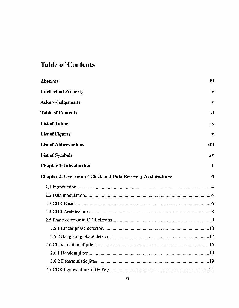
Table of Contents
Abstract iii
Intellectual Property iv
Acknowledgements v
Table of Contents vi
List of Tables ix
List of Figures x
List of Abbreviations xiii
List of Symbols xv
Chapter 1: Introduction 1
Chapter 2: Overview of Clock and Data Recovery Architectures 4
2.1 Introduction 4
2.2 Data modulation 4
2.3 CDR Basics 6
2.4 CDR Architectures 8
2.5 Phase detector in CDR circuits 9
2.5.1 Linear phase detector 10
2.5.2 Bang-bang phase detector 12
2.6 Classification of jitter 16
2.6.1 Random jitter 19
2.6.2 Deterministic jitter 19
2.7 CDR figures of merit (FOM) 21
vi
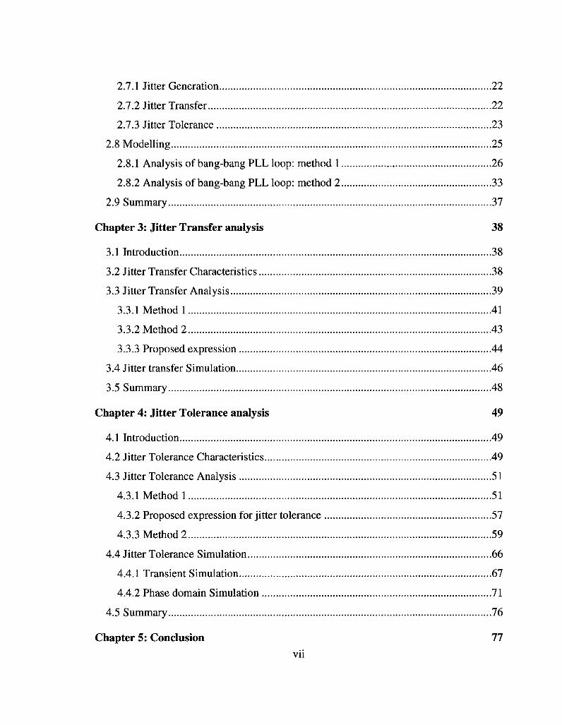
2.7.1 Jitter Generation 22
2.7.2 Jitter Transfer 22
2.7.3 Jitter Tolerance 23
2.8 Modelling 25
2.8.1 Analysis of bang-bang PLL loop: method 1 26
2.8.2 Analysis of bang-bang PLL loop: method 2 33
2.9 Summary 37
Chapter 3: Jitter Transfer analysis 38
3.1 Introduction 38
3.2 Jitter Transfer Characteristics 38
3.3 Jitter Transfer Analysis 39
3.3.1 Method 1 41
3.3.2 Method 2 43
3.3.3 Proposed expression 44
3.4 Jitter transfer Simulation 46
3.5 Summary 48
Chapter 4: Jitter Tolerance analysis 49
4.1 Introduction 49
4.2 Jitter Tolerance Characteristics 49
4.3 Jitter Tolerance Analysis 51
4.3.1 Method 1 51
4.3.2 Proposed expression for jitter tolerance 57
4.3.3 Method 2 59
4.4 Jitter Tolerance Simulation 66
4.4.1 Transient Simulation 67
4.4.2 Phase domain Simulation 71
4.5 Summary 76
Chapter 5: Conclusion 77
vii
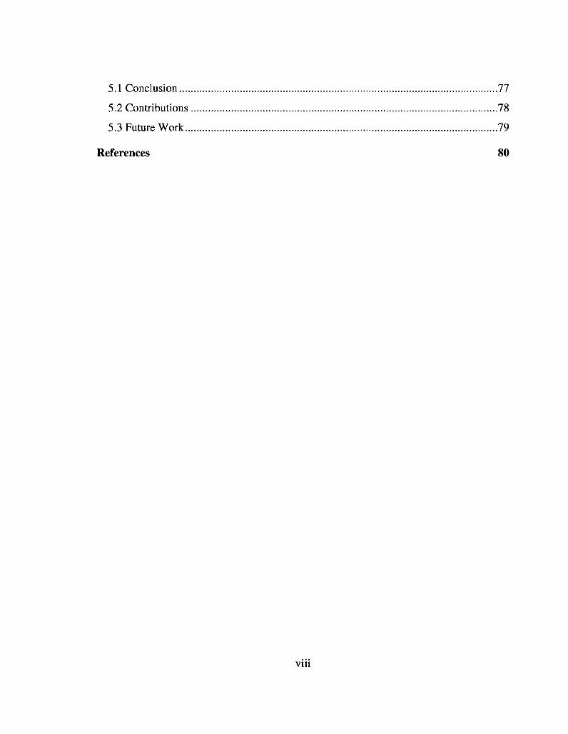
5.1 Conclusion 77
5.2 Contributions 78
5.3 Future Work 79
References 80
viii
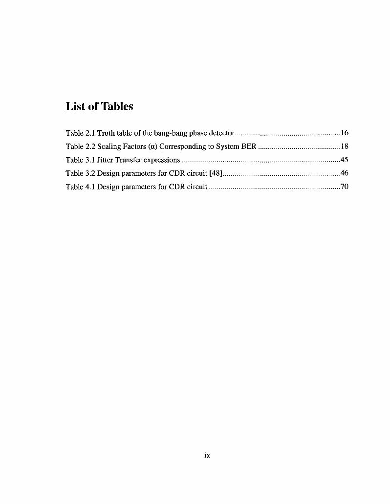
List of Tables
Table 2.1 Truth table of the bang-bang phase detector 16
Table 2.2 Scaling Factors (a) Corresponding to System BER 18
Table 3.1 Jitter Transfer expressions 45
Table 3.2 Design parameters for CDR circuit [48] 46
Table 4.1 Design parameters for CDR circuit 70
IX
List of Figures
Figure 2.1 Time-domain representation of unipolar RZ and NRZ line codes 5
Figure 2.2 Clock and data recovery 7
Figure 2.3 PLL based CDR circuit 8
Figure 2.4 Linear phase detector characteristic 9
Figure 2.5 Binary phase detector characteristic 10
Figure 2.6 Hogge phase detector 11
Figure 2.7 Waveforms of a Hogge phase detector 11
Figure 2.8 A CDR circuit with a DFF as the phase detector 13
Figure 2.9 Architecture of Alexander Phase detector circuit 14
Figure 2.10 Waveforms of an Alexander phase detector 15
Figure 2.11 Jitter definition 16
Figure 2.12 Eye diagram 17
Figure 2.13 Jitter subcomponents 18
Figure 2.14 PWD illustration 21
Figure 2.15 Jitter generation for OC-192 22
Figure 2.16 Jitter transfer mask for OC-192 23
Figure 2.17 Jitter tolerance mask for OC-192 25
Figure 2.18 Model for first order bang-bang PLL loop 27
Figure 2.19 Model of second order bang-bang PLL loop 28
Figure 2.20 Charge pump and loop filter equivalent circuit 30
Figure 2.21 Trade off in the frequency step, a>bb, for bang-bang PLL loop 31
Figure 2.22 Jitter tolerance curve for two different bang-bang frequency steps 31
Figure 2.23 Third order bang-bang PLL loop 32
Figure 2.24 Second order bang-bang PLL loop 33
x
Figure 2.25 Waveform used to determine the jitter transfer response 34
Figure 2.26 Jitter tolerance curve divided into two regions for analysis 34
Figure 2.27 Statistically averaged transfer function of bang-bang phase detector 35
Figure 2.28 Variations in jitter transfer curve due to RJ [43] 36
Figure 2.29 BER simulation results [43] 37
Figure 3.1 Jitter transfer measurement process where f, denotes the jitter transfer test
sinusoidal frequency 39
Figure 3.2 Bang-bang CDR circuit block diagram with two paths 40
Figure 3.3 Bang-bang PLL loop block diagram with analog filter 40
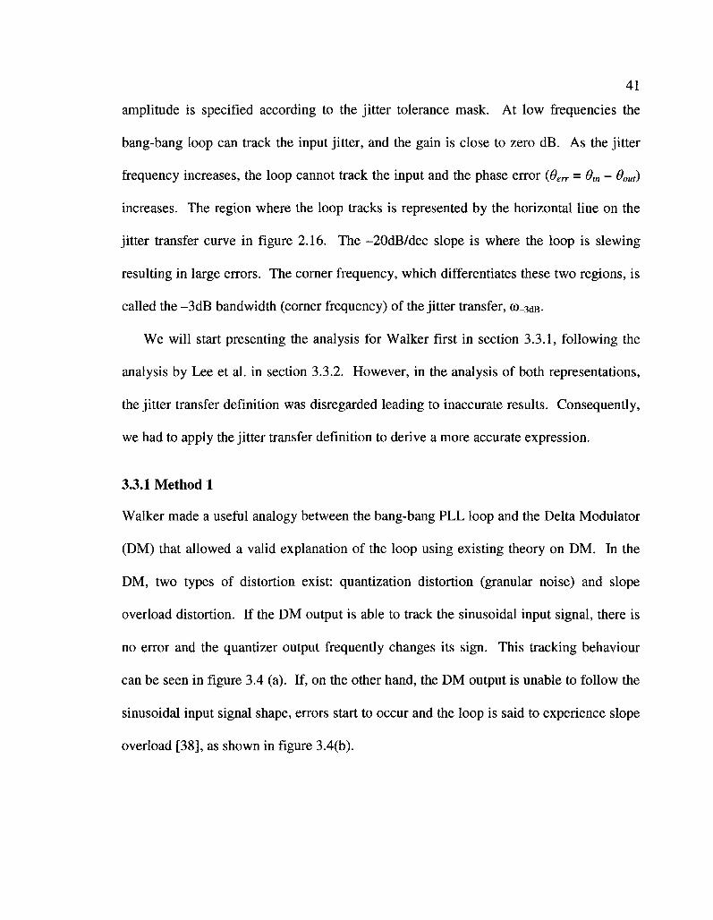
Figure 3.4 Slewing mechanism in PLL loop: (a) Onset of slewing, (b) Heavy slewing:
loop cannot track the input sinusoidal shape 42
Figure 3.5 CDR loop is slewing 44
Figure 3.6 Phase-domain testbench for second order bang-bang PLL loop 46
Figure 3.7 Predicted and simulated jitter transfer 47
Figure 3.8 Predicted (dotted) and simulated (solid) jitter transfer curves for different input
amplitudes 48
Figure 4.1 Maximum tolerable jitter Test [46] 50
Figure 4.2 Jitter tolerance mask 51
Figure 4.3 Second order bang-bang block diagram 1 52
Figure 4.4 (a) Block diagram II (a) Simplified block diagram II 53
Figure 4.5 Second order bang-bang block diagram III 55
Figure 4.6 Jitter tolerance curve for Walker equation 58
Figure 4.7 Jitter tolerance curve showing two regions 59
Figure 4.8 Jitter tolerance curve 60
Figure 4.9 Waveforms used to determine the jitter tolerance response 61
Figure 4.10 The jitter tolerance response of the first order loop 63
Figure 4.11 Waveforms showing the integral response provided by the capacitor 64
Figure 4.12 Test bench for Jitter tolerance simulation 67
Figure 4.13 PRBS7 with sinusoidal input jitter 68
xi
Figure 4.14 Linear Feedback Shift Register 68
Figure 4.15 Second order bang-bang CDR circuit used in Simulation 69
Figure 4.16 BER error detection 69
Figure 4.17 Simulated and derived jitter tolerance curve 71
Figure 4.18 Phase domain model testbench 71
Figure 4.19 Jitter tolerance curve from phase-domain simulation 72
Figure 4.20 Simulation results for an input signal of 0.5UI at high frequencies 73
Figure 4.21 Simulation results for an input signal of 0.79UI in Region 1 74
Figure 4.22 Simulation results for an input signal of 9.93UI in Region II 75
Figure 4.23 Simulation results for an input signal of 9.94UI in Region II 76
xn
List of Abbreviations
BB
BER
BPF
CDR
CP
DCD
DDJ
DFF
DJ
DLL
DM
DPLL
DUT
FOM
IL
ISI
LF
LFSR
Bang-bang
Bit Error Rate
Band-pass filter
Clock and Data Recovery
Charge pump
Duty cycle distortion
Data dependant jitter
D Flip-flop
Deterministic jitter
Delay locked loop
Delta modulator
Digital phase locked loop
Device under test
Figure of merit
Injection locking
Inter symbol interference
Loop filter
Linear feedback shift register
xiii
NRZ
PD
PI
PJ
PLL
PRBS
PWD
RJ
RMS
RZ
SDM
SJ
SONET
UI
vco
Non-return-to-zero
Phase detector
Phase interpolator
Periodic Jitter
Phase locked loop
Pseudo-random bit sequence
Pulse width distortion
Random jitter
Root-mean-square
Return-to-zero
Sigma-delta modulator
Sinusoidal jitter
Synchronous optical network
Unit interval
Voltage controlled oscillator
XIV
List of Symbols
A w
A0ut
C
I
JG
Jtol
Jtolj
Jtoh
Jtolw
Jtrans
Kv
r
R
tdelay
Tj
tn
a
P
Input jitter amplitude
Output jitter amplitude
Loop filter capacitance
Charge pump current
Jitter generation function
Jitter tolerance function
Lee et al.'s Jitter tolerance function for region I
Lee et al.'s Jitter tolerance function for region II
Walker's Jitter tolerance function
Jitter transfer function
VCO gain in rad/sec/volt
Data rate
Loop filter resistance
Delay in a PLL loop
Input jitter period
Sampling period
Integration path gain
Proportional path gain in Volts
XV
s
AVbb
AVin
AVM
A6
Avintegral
A Umax
At)proportional
8co
Aco
s
c O'JO
9'out(t)
dbb
t'err
dm
Gout
<P(t)
Oi-UB
Oibb
COc
Arbitrary Phase Offset
Proportional path control voltage
VCO control voltage
Integral path control voltage
Proportional path phase step
Integral path phase step
Maximum phase error
Proportional path phase step
Input jitter frequency variation component
Integral path frequency step
±1
Stability factor
Slope of the input phase signal
Slope of the output phase signal
Bang-bang phase step
Phase error
Input phase
Output phase
Input jitter phase variation component
Jitter transfer -3dB bandwidth
Bang-bang radian frequency step
VCO center frequency
XVI
co,„ Input data frequency
coj Input j itter radian frequency
coL Lee et al. ' s corner frequency for jitter transfer
oi0 Output frequency
covco VCO frequency
cow Walker's corner frequency for jitter transfer
xvii
Chapter l: Introduction
The continued increase in the speed of the internet has created a pressing need for high
speed communication systems. Serial communication is well suited for long distances,
because fewer wires are used as compared to parallel communication. Serial
communication systems require clock generation, multiplexing, clock recovery,
demultiplexing and loss of signal detection. A clock and data recovery circuit (CDR) is
an essential block used as part of the receiver of high-speed serial communication system
and synchronous optical network (SONET). With the increasing interest in multi-gigabit
per second links, CDR circuits have to meet strict jitter and stability requirements.
CDR circuits can be categorized into two groups according to their phase detector
type: the linear CDR and the binary (bang-bang) CDR. While linear phase detector-
based CDR circuits have proven to be suitable for meeting system requirements, the
performance of this group of phase detectors descends as the data rates reach the speed
limits of existing technology. More specifically, the linear phase detector produces
narrow pulses proportional to the phase error between the incoming data and the clock.
These narrow pulses require technology process speed much higher than the sampling
frequency.
2
Bang-bang phase detector-based CDR circuits are becoming the common design
choice for state-of-the CDR designs for three reasons. First, they are very simple in
structure and can operate at much higher speeds than their linear counterparts. Secondly,
they experience no static phase error due to the inherent sampling phase alignment.
Finally, they adapt to multi-phase sampling structures, which allows for operation at
frequencies at a fraction of the data rate. As a result of these advantages of the bang-bang
CDRs, there is a marked increase in designs employing them. A survey of CDR designs
at the International Solid State Circuits Conference showed that as the design data rate
approach the speed limitation of the technology, it is more likely to implement a bang-
bang CDR [1].
Despite its increasing popularity, the bang-bang CDR's nonlinear behaviour makes it
difficult to analyze. Lack of complete analysis of the bang-bang CDR circuit adds
complexity to the design. More simulations and prototypes are required in order to meet
required specifications. As a result more resources and time are wasted. Some effort has
been made in the last decade to develop models to characterize the CDR's nonlinear
behaviour more accurately. Different models were introduced and the analysis
methodologies are quite different resulting in a need to compare and validate the different
models.
In this work we provide a more detailed analysis on second order bang-bang CDR
circuits. We will present a detailed analysis of jitter transfer and jitter tolerance using
existing models. In the case of jitter transfer analysis, a more accurate expression is
derived and verified by behavioural simulation. The proposed expression complies with
3
the definition. As for the jitter tolerance analysis, simulation test benches are developed
and used to verify the validity of existing models. A simplified expression for jitter
tolerance is proposed based on method 1. Limitations of existing models in different
regions of the jitter tolerance curve are explained and illustrated by simulation results.
Background information on linear and bang-bang CDR circuits from both the
architectural and circuit level is presented in chapter 2. Next, figure of merits (FOM)
used to measure the performance of CDR circuits are presented. Finally, different
models for bang-bang CDR circuits are illustrated and expressions are derived. Analysis
for jitter transfer based on the two major methods is introduced in chapter 3 where a more
accurate expression for jitter transfer is derived and verified by behavioural simulation.
Chapter 4 introduces the jitter tolerance analysis for a second order bang-bang CDR
circuit in which time-domain and phase-domain test benches are developed and used to
explain the loop dynamics in different regions of the jitter tolerance curve. Finally,
chapter 5 summarizes the thesis, clarifies the major contributions and points to potential
future work.
4
Chapter 2: Overview of Clock and Data Recovery Architectures
2.1 Introduction
The CDR circuit is a key element in high-speed serial links and as a result there have
been a tremendous research going on designing different architectures of CDR circuits to
enhance speed, accuracy, chip area, power and jitter characteristics. In this chapter, a
background on CDR architectures and their main operation principles are reviewed.
CDR architectures can be classified into three main categories, according to the
relationship between the input phase signal and the output. In order to compare between
CDR circuits, there are FOMs to characterize the performance of different CDR circuits,
such as jitter tolerance, jitter transfer and jitter generation. After presenting a review on
the jitter characteristics, different methods for modeling and analyzing the bang-bang
CDR circuit are investigated. Two main methods for modeling and analyzing the bang-
bang CDR circuit are discussed in more details with an overview on previous work done.
2.2 Data modulation
In communication systems, transmitted data is usually modulated or encoded in order to
make it easier to receive the data, or in order to enable error correction. While
modulation is more commonly associated with wireless data communication, it is merely
5
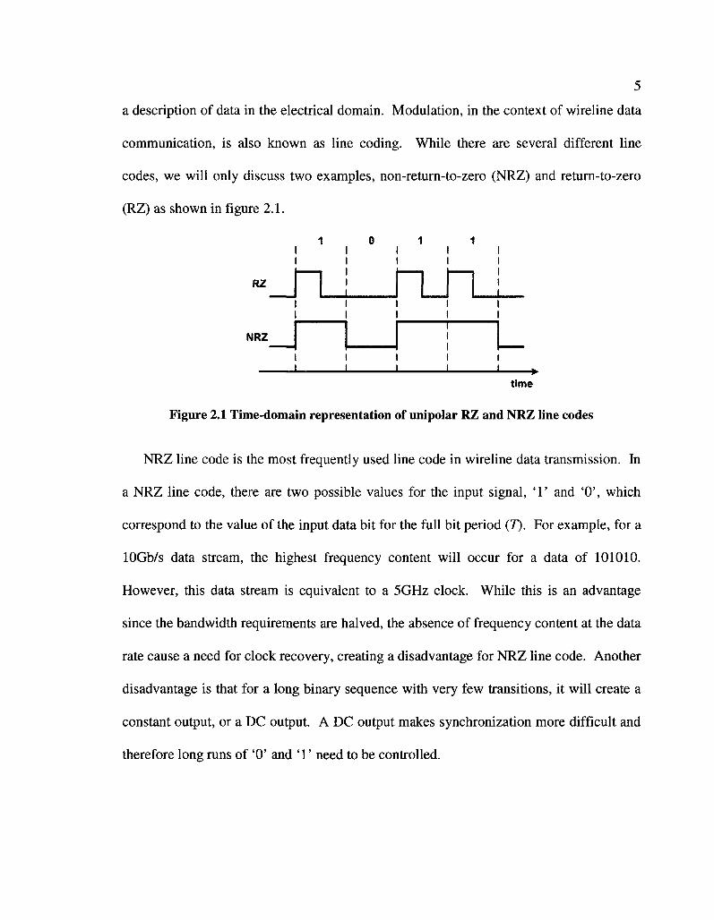
a description of data in the electrical domain. Modulation, in the context of wireline data
communication, is also known as line coding. While there are several different line
codes, we will only discuss two examples, non-return-to-zero (NRZ) and return-to-zero
(RZ) as shown in figure 2.1.
1 0 1 1 i i i i i i i i i i
~_n_L_rL_m_ i i i i i i i i i i
NRZ I
I I I I I 1 1 1 1 1 ^
time
Figure 2.1 Time-domain representation of unipolar RZ and NRZ line codes
NRZ line code is the most frequently used line code in wireline data transmission. In
a NRZ line code, there are two possible values for the input signal, ' 1 ' and '0', which
correspond to the value of the input data bit for the full bit period (T). For example, for a
lOGb/s data stream, the highest frequency content will occur for a data of 101010.
However, this data stream is equivalent to a 5GHz clock. While this is an advantage
since the bandwidth requirements are halved, the absence of frequency content at the data
rate cause a need for clock recovery, creating a disadvantage for NRZ line code. Another
disadvantage is that for a long binary sequence with very few transitions, it will create a
constant output, or a DC output. A DC output makes synchronization more difficult and
therefore long runs of '0' and ' 1' need to be controlled.
6
In RZ line code, the data bit is represented in the first half of the bit period (7). In the
second half, the output signal returns to its neutral level (where the neutral level is at zero
voltage). Thus, a data bit of ' 1 ' is represented by a positive voltage, while a data bit of
'0' is represented by a zero voltage, in unipolar RZ or a negative voltage in bipolar RZ.
This makes data synchronization much easier as the signal has spectral power at the
frequency equal to the data rate. Another benefit of the RZ code is that there are always
transitions, indicating that the data signal will never be blocked by high-pass filtering
with long runs of ' 1 ' or '0'. However, the main drawback of this line code is that it
requires twice the bandwidth of NRZ.
Transmitted binary data are often encoded in wireline systems to overcome some
issues. One such issue results when the lack of transitions during a long run causes the
oscillator to drift and generate jitter. Encoding avoids this issue by limiting the number
of consecutive T s or '0's. For example, 8B/10B coding converts a sequence of 8 bits to
10 bits while guaranteeing a maximum run length of 5 bits. In addition, encoding the
data allows the new data signal to maintain DC balance by guaranteeing that there are an
equal number of Ts and "0's [2]. The 8B/10B code provides the benefits of guaranteed
transitions and DC balance described above and hence is employed in a number of
standards. A more efficient version, called 64B/66B coding is also used in other
standards to lower the overhead to 3% as opposed to 25% overhead in 8B/10B coding.
2.3 CDR Basics
A random data stream has a unique interpretation only if a time reference is provided for
synchronization. In serial data communications, the incoming data is first synchronized
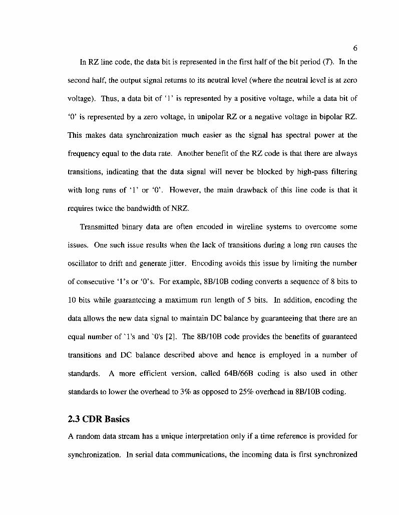
to an internal clock and then retimed in order to remove jitter accumulation. CDR circuit
is responsible to recover the clock from the incoming data stream and then use this clock
to retime the data, as shown in figure 2.2 [2]. The retimed data, with no errors, is
logically the same as the input data stream but with less jitter.
Incoming data
Clock Recovery
n O
CLK
k Retimed data
Figure 2.2 Clock and data recovery
We have seen in the last section that the data spectrum for NRZ line code does not
contain any energy at the data rate. In order to allow recovery of the clock information
contained in the data stream, energy must be created by a nonlinear operation, like edge
detection, at the input of the CDR [2]. Edge detection is a combination of differentiation
and rectification. Several phase detector circuit topologies for phase-locked loops (PLL)
operating on random data streams have been developed. These structures, performing
implicit edge detection at the input of the PLL, are discussed in more detail in [2].
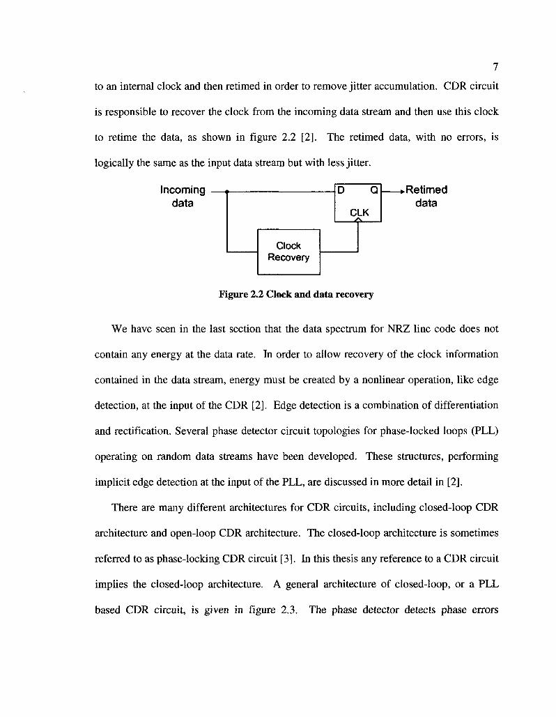
There are many different architectures for CDR circuits, including closed-loop CDR
architecture and open-loop CDR architecture. The closed-loop architecture is sometimes
referred to as phase-locking CDR circuit [3]. In this thesis any reference to a CDR circuit
implies the closed-loop architecture. A general architecture of closed-loop, or a PLL
based CDR circuit, is given in figure 2.3. The phase detector detects phase errors
8
between the incoming data signal and the internal clock signal and supplies correction
information to the charge pump. The charge pump takes the correction information and
adds charge to or subtracts charge from the loop filter. The loop filter plays an important
role in defining the frequency response of the system. The voltage on the loop filter
controls the VCO, and the output of the VCO is sent to both the phase detector and also
to the retiming circuit. More details on CDR circuit architectures are given in the
following section.
Incomina data
Phase Detector
Charge Pump Loop Filter VCO
r> <-»
CLK
Retimed data
Recovered Clock
Figure 2.3 PLL based CDR circuit
2.4 CDR Architectures
There is a wide variety of CDR architectures have been proposed for high speed data
transmission applications, such as CDR architectures based on analog PLL, digital PLL
(DPLL), delay locked loop (DLL), phase interpolator (PI), injection locking (IL),
oversampling, gate oscillator, and high-Q bandpass filter [4-11]. CDR architectures can
be classified into three main types, the analog, semi-analog, and the all digital CDR
architectures. Another classification is according to the phase relationship between the
input data and the local clock at the receiver [12]. We can divide them into three
categories:
1. Feedback phase tracking architectures such as PLL, DLL, PI, and IL.
9
2. Oversampling based CDR architecture.
3. Phase alignment without feedback phase tracking architecture such as gated
oscillator and high-Q band pass filtering.
In each of the above categories, the CDR architectures can be further divided into
subgroups. For more details, the reader is advised to refer to [12].
2.5 Phase detector in CDR circuits
In this section we will classify CDR circuits according to the phase detector type. CDR
circuits employ two types of phase detectors, linear phase detectors and binary phase
detectors. A linear phase detector (PD) compares the phase of the incoming data with the
phase of the clock generated from the VCO. The linear PD generates an output that is
proportional to the magnitude of the phase difference, hence the name linear. The linear
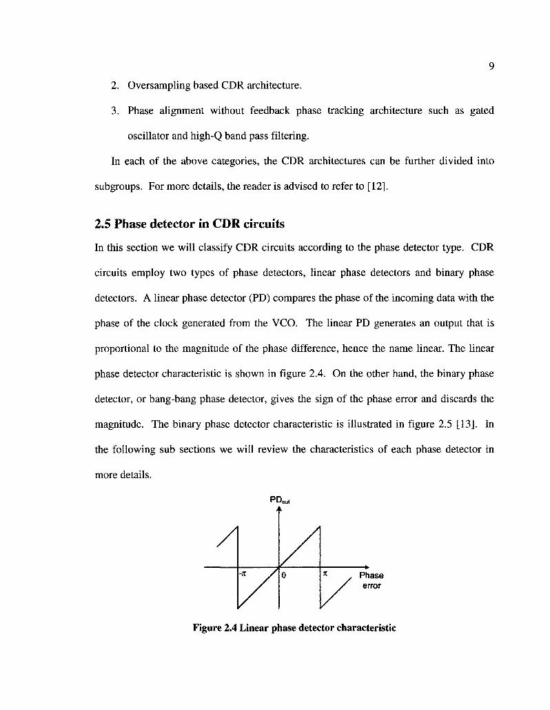
phase detector characteristic is shown in figure 2.4. On the other hand, the binary phase
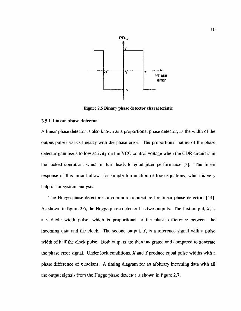
detector, or bang-bang phase detector, gives the sign of the phase error and discards the
magnitude. The binary phase detector characteristic is illustrated in figure 2.5 [13]. In
the following sub sections we will review the characteristics of each phase detector in
more details.
PDo u !
/
1
-7t /
k
0 * / Ph
Figure 2.4 Linear phase detector characteristic
10
PDou,
/
-n 0
-/
K *
Pha err<
Figure 2.5 Binary phase detector characteristic
2.5.1 Linear phase detector
A linear phase detector is also known as a proportional phase detector, as the width of the
output pulses varies linearly with the phase error. The proportional nature of the phase
detector gain leads to low activity on the VCO control voltage when the CDR circuit is in
the locked condition, which in turn leads to good jitter performance [3]. The linear
response of this circuit allows for simple formulation of loop equations, which is very
helpful for system analysis.
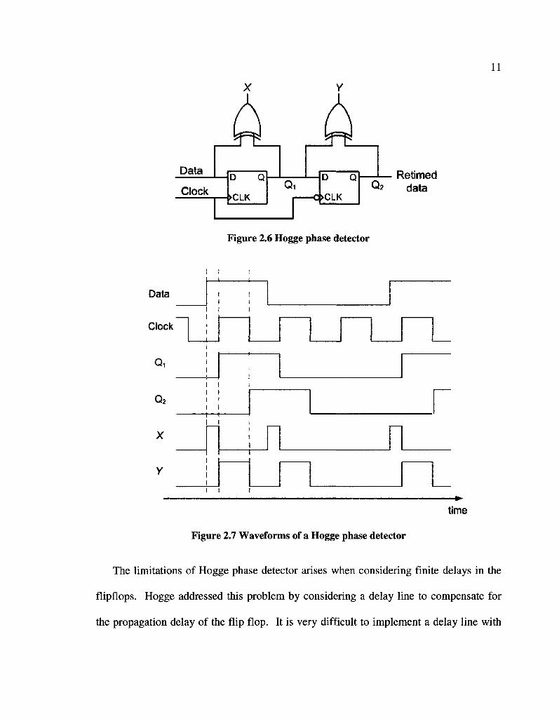
The Hogge phase detector is a common architecture for linear phase detectors [14].
As shown in figure 2.6, the Hogge phase detector has two outputs. The first output, X, is
a variable width pulse, which is proportional to the phase difference between the
incoming data and the clock. The second output, Y, is a reference signal with a pulse
width of half the clock pulse. Both outputs are then integrated and compared to generate
the phase error signal. Under lock conditions, X and Y produce equal pulse widths with a
phase difference of n radians. A timing diagram for an arbitrary incoming data with all
the output signals from the Hogge phase detector is shown in figure 2.7.
11
Data
Clock D Q
>CLK Qi
D Q
>CLK Q2
- Retimed data
Data
Clock
Qi
Q2
Figure 2.6 Hogge phase detector
i i
I ! I \ I ' I I
1 — t -
time
Figure 2.7 Waveforms of a Hogge phase detector
The limitations of Hogge phase detector arises when considering finite delays in the
flipflops. Hogge addressed this problem by considering a delay line to compensate for
the propagation delay of the flip flop. It is very difficult to implement a delay line with
12
process, voltage and temperature variations in modern high speed processes. Several
papers [15,16] have improved the Hogge phase detector to overcome this limitation.
Although they show some performance improvements, they still have limitations in high
speed processes.
A common drawback of using linear phase detectors with setup times that are
different from retiming flip-flops is that the recovered clock will not be intrinsically
aligned in the optimum sampling point in the data eye. Another drawback is that the
linear phase detector produces narrow pulses proportional to the phase error. These
narrow pulses are very difficult to generate at high data rates. Both the setup/hold times
and narrow pulses are the limiting factors to realize high speed CDR using a linear phase
detector. Alternative techniques for utilizing a high speed CDR using a linear phase
detector are reported in [17-20].
2.5.2 Bang-bang phase detector
The binary phase detector, or bang-bang phase detector, has two output states as shown in
figure 2.5. Unlike the linear phase detector, the output of the bang-bang phase detector
gives information on the polarity of the phase error rather than the magnitude. The bang-
bang phase detector is usually used in many CDR circuit designs due to its ability to work
at a much higher speed than the linear phase detector [1]. In our discussion we will
present the simplest bang-bang phase detector, D-flipflop (DFF), and the most common
binary PD, the Alexander phase detector.
The simplest binary phase detector is a DFF where the incoming data samples the
clock generated by the VCO, as illustrated in Figure 2.8 [21]. The output of the phase
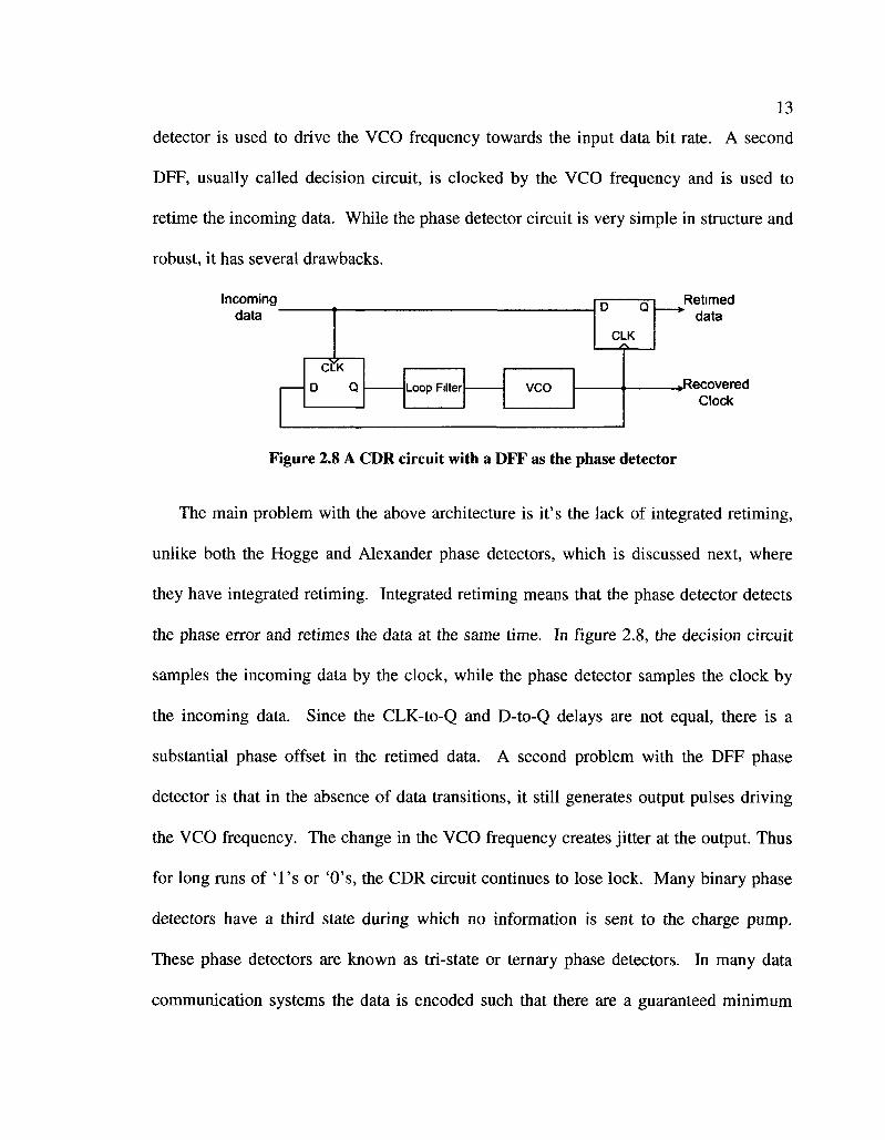
13
detector is used to drive the VCO frequency towards the input data bit rate. A second
DFF, usually called decision circuit, is clocked by the VCO frequency and is used to
retime the incoming data. While the phase detector circuit is very simple in structure and
robust, it has several drawbacks.
Incoming data
CLK
D Q Loop Filter VCO
n o
CLK
I
»f
Retimed data
Recovered Clock
Figure 2.8 A CDR circuit with a DFF as the phase detector
The main problem with the above architecture is it's the lack of integrated retiming,
unlike both the Hogge and Alexander phase detectors, which is discussed next, where
they have integrated retiming. Integrated retiming means that the phase detector detects
the phase error and retimes the data at the same time. In figure 2.8, the decision circuit
samples the incoming data by the clock, while the phase detector samples the clock by
the incoming data. Since the CLK-to-Q and D-to-Q delays are not equal, there is a
substantial phase offset in the retimed data. A second problem with the DFF phase
detector is that in the absence of data transitions, it still generates output pulses driving
the VCO frequency. The change in the VCO frequency creates jitter at the output. Thus
for long runs of T s or 'O's, the CDR circuit continues to lose lock. Many binary phase
detectors have a third state during which no information is sent to the charge pump.
These phase detectors are known as tri-state or ternary phase detectors. In many data
communication systems the data is encoded such that there are a guaranteed minimum
14
number of transitions, in which case there would be a limited number of repeated vl's or
v0's and the absence of a tri-state phase detector would not limit the performance.
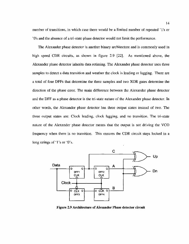
The Alexander phase detector is another binary architecture and is commonly used in
high speed CDR circuits, as shown in figure 2.9 [22]. As mentioned above, the
Alexander phase detector inherits data retiming. The Alexander phase detector uses three
samples to detect a data transition and weather the clock is leading or lagging. There are
a total of four DFFs that determine the three samples and two XOR gates determine the
direction of the phase error. The main difference between the Alexander phase detector
and the DFF as a phase detector is the tri-state nature of the Alexander phase detector. In
other words, the Alexander phase detector has three output states instead of two. The
three output states are: Clock leading, clock lagging, and no transition. The tri-state
nature of the Alexander phase detector means that the output is not driving the VCO
frequency when there is no transition. This ensures the CDR circuit stays locked in a
long strings of T s or 'O's.
Data D Q
DFF1 CLK
<*»
Clock —i >
D CLK Q DFF3
D 0. DFF2 CLK
D CLK Q DFF4
B
Up
Dn
Figure 2.9 Architecture of Alexander Phase detector circuit
15
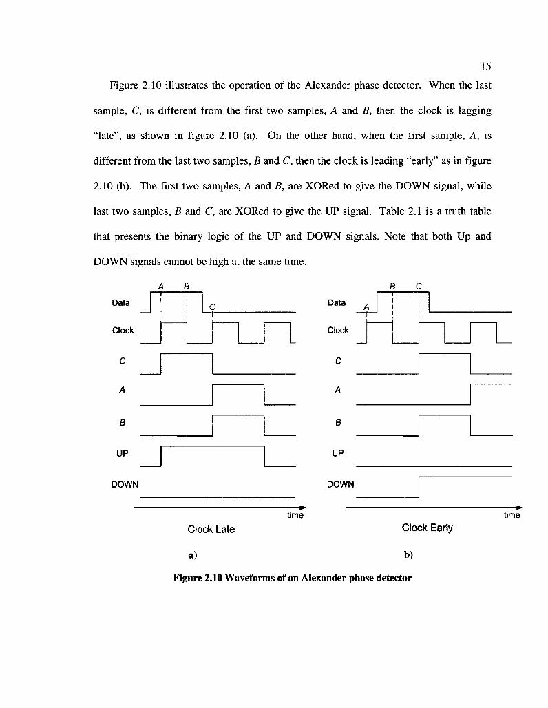
Figure 2.10 illustrates the operation of the Alexander phase detector. When the last
sample, C, is different from the first two samples, A and B, then the clock is lagging
"late", as shown in figure 2.10 (a). On the other hand, when the first sample, A, is
different from the last two samples, B and C, then the clock is leading "early" as in figure
2.10 (b). The first two samples, A and B, are XORed to give the DOWN signal, while
last two samples, B and C, are XORed to give the UP signal. Table 2.1 is a truth table
that presents the binary logic of the UP and DOWN signals. Note that both Up and
DOWN signals cannot be high at the same time.
A B B C —r 1—I |—
Data [ | c Data , i j
Clock Clock
A -T
B
UP
B
UP
DOWN DOWN
time
Clock Late Clock Early
a) b)
Figure 2.10 Waveforms of an Alexander phase detector
time
16
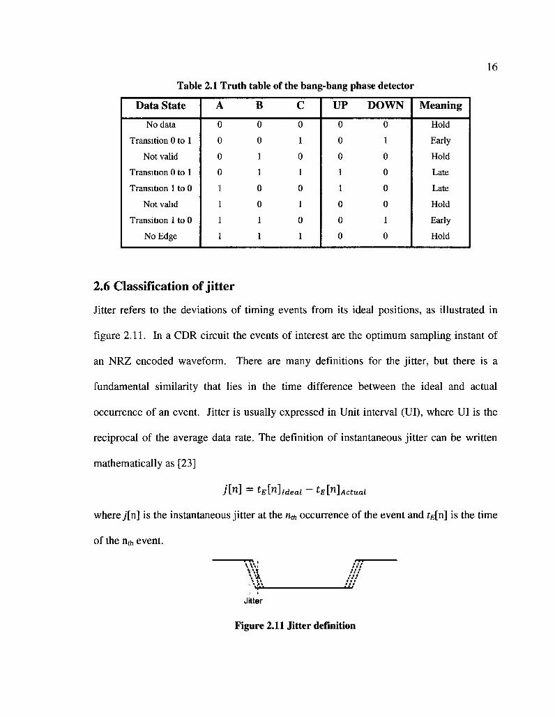
Table 2.1 Truth table of the bang-bang phase detector
Data State
No data
Transition 0 to 1
Not valid
Transition 0 to 1
Transition 1 to 0
Not valid
Transition 1 to 0
No Edge
A
0
0
0
0
1
1
1
1
B
0
0
1
1
0
0
1
1
C
0
1
0
1
0
1
0
1
UP
0
0
0
1
1
0
0
0
DOWN
0
1
0
0
0
0
1
0
Meaning
Hold
Early
Hold
Late
Late
Hold
Early
Hold
2.6 Classification of jitter
Jitter refers to the deviations of timing events from its ideal positions, as illustrated in
figure 2.11. In a CDR circuit the events of interest are the optimum sampling instant of
an NRZ encoded waveform. There are many definitions for the jitter, but there is a
fundamental similarity that lies in the time difference between the ideal and actual
occurrence of an event. Jitter is usually expressed in Unit interval (UI), where UI is the
reciprocal of the average data rate. The definition of instantaneous jitter can be written
mathematically as [23]
j[n] = tE[ri\ideai — tE[n]Actuai
where y'[n] is the instantaneous jitter at the nth occurrence of the event and fc[n] is the time
of the nth event.
TO' .77 * * S \ I * M m • 11 * * t
\ \\ * * * * . . d * P » » t » ' *|" "' J I
Jitter
Figure 2.11 Jitter definition
17
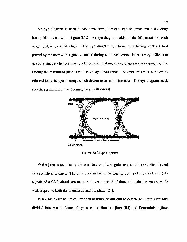
An eye diagram is used to visualize how jitter can lead to errors when detecting
binary bits, as shown in figure 2.12. An eye-diagram folds all the bit periods on each
other relative to a bit clock. The eye diagram functions as a timing analysis tool
providing the user with a good visual of timing and level errors. Jitter is very difficult to
quantify since it changes from cycle to cycle, making an eye diagram a very good tool for
finding the maximum jitter as well as voltage level errors. The open area within the eye is
referred to as the eye opening, which decreases as errors increase. The eye diagram mask
specifies a minimum eye opening for a CDR circuit.
A M 11 Unit Interval w
Voltge Noise
Figure 2.12 Eye diagram
While jitter is technically the non-ideality of a singular event, it is most often treated
in a statistical manner. The difference in the zero-crossing points of the clock and data
signals of a CDR circuit are measured over a period of time, and calculations are made
with respect to both the magnitude and the phase [24].
While the exact nature of jitter can at times be difficult to determine, jitter is broadly
divided into two fundamental types, called Random jitter (RJ) and Deterministic jitter
18
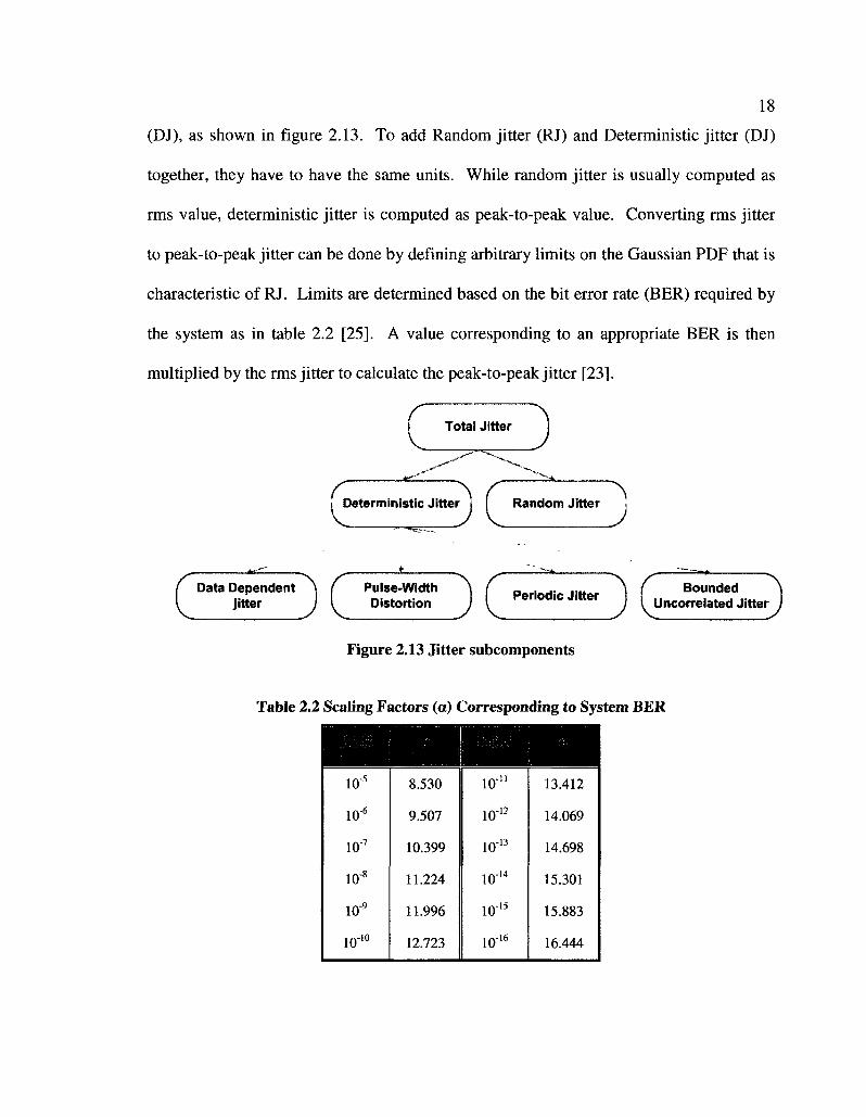
(DJ), as shown in figure 2.13. To add Random jitter (RJ) and Deterministic jitter (DJ)
together, they have to have the same units. While random jitter is usually computed as
rms value, deterministic jitter is computed as peak-to-peak value. Converting rms jitter
to peak-to-peak jitter can be done by defining arbitrary limits on the Gaussian PDF that is
characteristic of RJ. Limits are determined based on the bit error rate (BER) required by
the system as in table 2.2 [25]. A value corresponding to an appropriate BER is then
multiplied by the rms jitter to calculate the peak-to-peak jitter [23].
Total Jitter
r. C Deterministic Jitter Random Jitter J
Data Dependent jitter
Pulse-Width Distortion Periodic Jitter Bounded
Uncorrected Jitter
Figure 2.13 Jitter subcomponents
Table 2.2 Scaling Factors (a) Corresponding to System BER
IO"5
IO"6
io-7
10"8
IO"9
1 0- io
8.530
9.507
10.399
11.224
11.996
12.723
IO'11
1 0 ] 2
10 1 3
IO"14
10 1 5
IO'16
13.412
14.069
14.698
15.301
15.883
16.444
19
2.6.1 Random jitter
Random jitter (RJ) is unpredictable and has a Gaussian probability density function. The
causes of RJ are generally due to device noise sources such as shot noise [24,26]. Shot
noise is related to the fluctuation in current flow in a transistor. Thermal noise is another
component of device noise. Electron scattering causes thermal noise when electrons
move through a conducting medium and collide with silicon atoms or impurities in the
lattice. Higher temperatures results in greater atoms vibrations and increases chances of
collisions. Another component of device noise is flicker noise, or 1/frequency noise. It is
caused by the random capture and emission of carriers from oxide interface traps
affecting carrier density in a transistor.
As random jitter is statistical in nature and has a Gaussian PDF. A Gaussian
distribution is unbounded by definition and is characterized by its mean and rms values.
As a result, random jitter measurements for separate system components cannot be directly
added, but may be combined by taking the square-root of the sum of the squares.
2.6.2 Deterministic jitter
Deterministic jitter describes timing variations that have identifiable causes and bounded
in amplitude. The sources of deterministic jitter include limited bandwidth, signal
reflection, duty-cycle distortion, cross talk, and power-supply noise. Deterministic jitter
can be divided into four categories: Data Dependent Jitter (DDJ), Pulse Width Distortion
(PWD), Periodic Jitter (PJ) and Bounded Uncorrelated Jitter [23].
20
2.6.2.1. Data dependent jitter (DDJ)
Data Dependent Jitter (DDJ) and Intersymbol Interference (ISI) are two different names
for the same type of jitter, viewed from the perspective of time and frequency,
respectively. DDJ refers to jitter from a time-domain perspective. DDJ is the timing
jitter that is correlated with the bit sequence in a data stream. In other words, the
response of the current bit is affected by the response of the previous bits. DDJ is caused
by limited bandwidth.
ISI refers to jitter from a frequency-domain perspective. It is defined as pulse
spreading due to limitation in the system bandwidth. When the system bandwidth is
approximately the same as the bandwidth required by the pulse, then the pulse are spread
into adjacent bit times, causing errors in interpretation of binary bits.
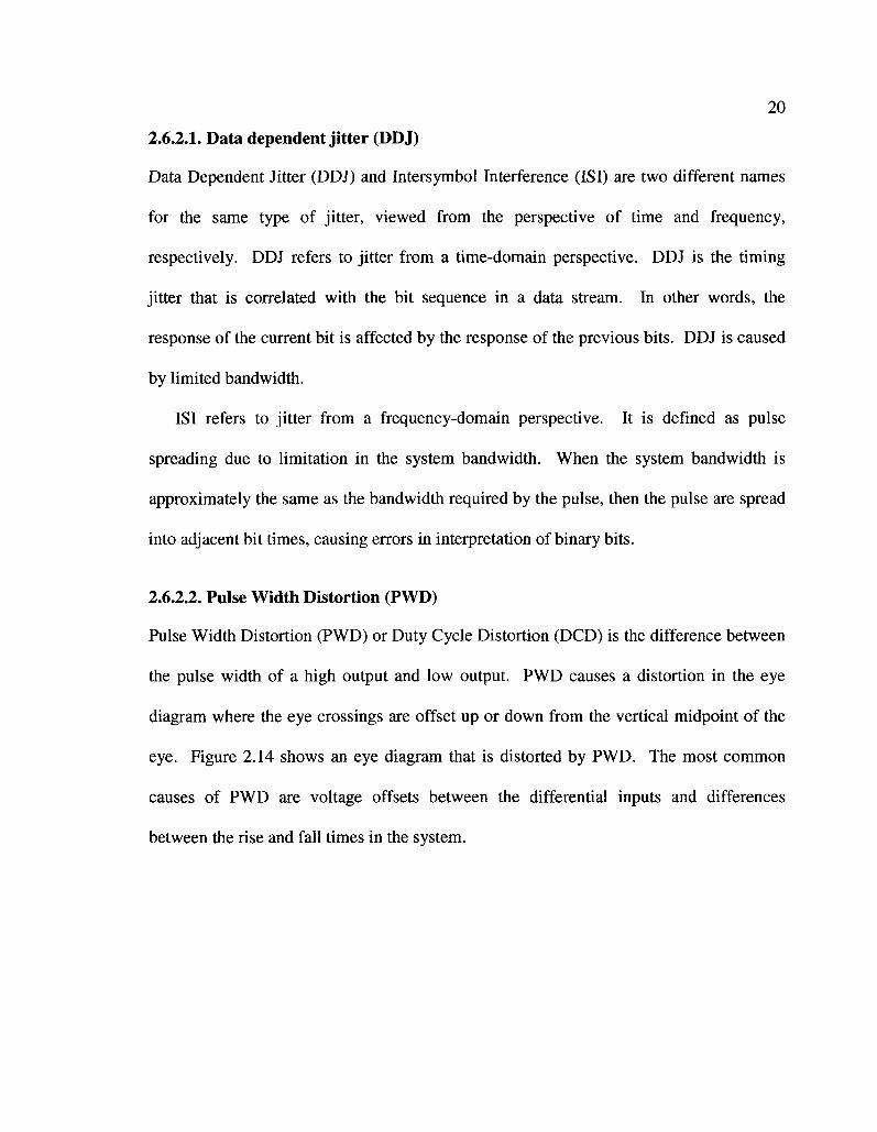
2.6.2.2. Pulse Width Distortion (PWD)
Pulse Width Distortion (PWD) or Duty Cycle Distortion (DCD) is the difference between
the pulse width of a high output and low output. PWD causes a distortion in the eye
diagram where the eye crossings are offset up or down from the vertical midpoint of the
eye. Figure 2.14 shows an eye diagram that is distorted by PWD. The most common
causes of PWD are voltage offsets between the differential inputs and differences
between the rise and fall times in the system.
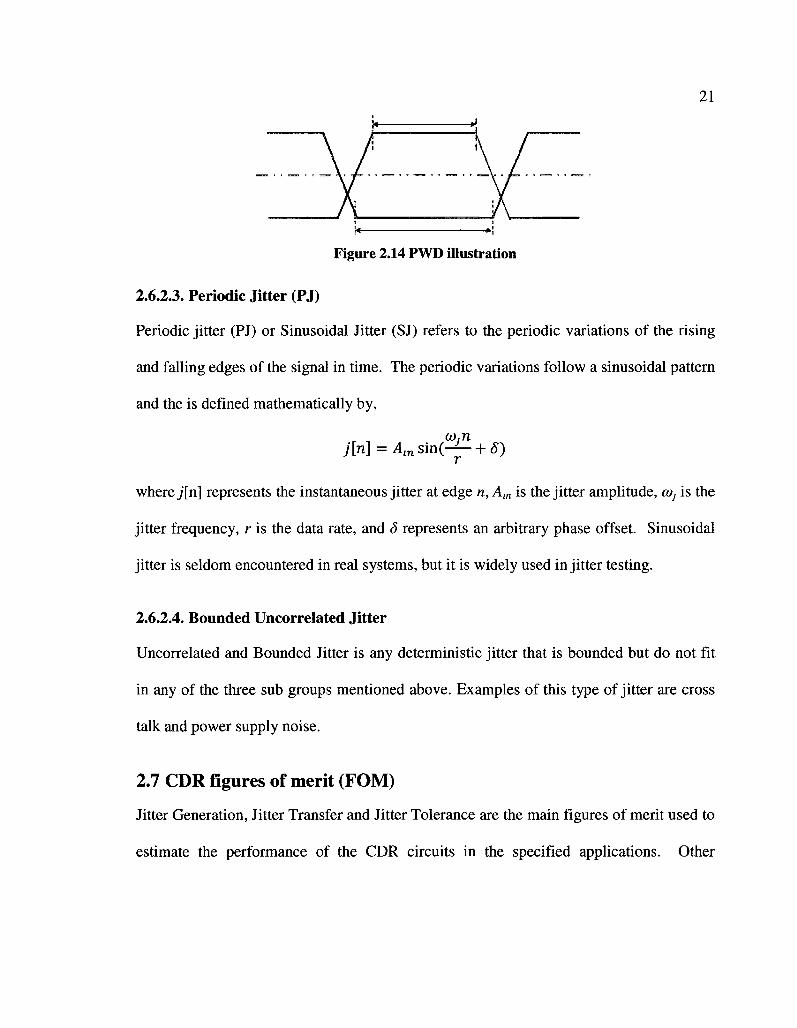
21
Figure 2.14 PWD illustration
2.6.2.3. Periodic Jitter (PJ)
Periodic jitter (PJ) or Sinusoidal Jitter (SJ) refers to the periodic variations of the rising
and falling edges of the signal in time. The periodic variations follow a sinusoidal pattern
and the is defined mathematically by,
(ii,n j[n]=Ainsin(-jr + 8)
where y[n] represents the instantaneous jitter at edge n, Am is the jitter amplitude, a)j is the
jitter frequency, r is the data rate, and d represents an arbitrary phase offset. Sinusoidal
jitter is seldom encountered in real systems, but it is widely used in jitter testing.
2.6.2.4. Bounded Uncorrelated Jitter
Uncorrelated and Bounded Jitter is any deterministic jitter that is bounded but do not fit
in any of the three sub groups mentioned above. Examples of this type of jitter are cross
talk and power supply noise.
2.7 CDR figures of merit (FOM)
Jitter Generation, Jitter Transfer and Jitter Tolerance are the main figures of merit used to
estimate the performance of the CDR circuits in the specified applications. Other
22
common FOM are BER, power consumption, chip area and operating frequency. In this
section we only focus on Jitter Generation, Jitter Transfer and Jitter Tolerance.
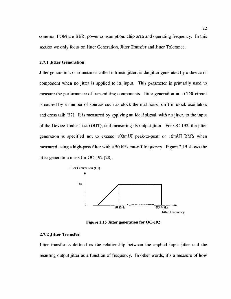
2.7.1 Jitter Generation
Jitter generation, or sometimes called intrinsic jitter, is the jitter generated by a device or
component when no jitter is applied to its input. This parameter is primarily used to
measure the performance of transmitting components. Jitter generation in a CDR circuit
is caused by a number of sources such as clock thermal noise, drift in clock oscillators
and cross talk [27]. It is measured by applying an ideal signal, with no jitter, to the input
of the Device Under Test (DUT), and measuring its output jitter. For OC-192, the jitter
generation is specified not to exceed lOOmUI peak-to-peak or lOmUI RMS when
measured using a high-pass filter with a 50 kHz cut-off frequency. Figure 2.15 shows the
jitter generation mask for OC-192 [28].
Jitter Generation (LI)
0 01
50KH? SO MHz Jitter Frequency
Figure 2.15 Jitter generation for OC-192
2.7.2 Jitter Transfer
Jitter transfer is defined as the relationship between the applied input jitter and the
resulting output jitter as a function of frequency. In other words, it's a measure of how
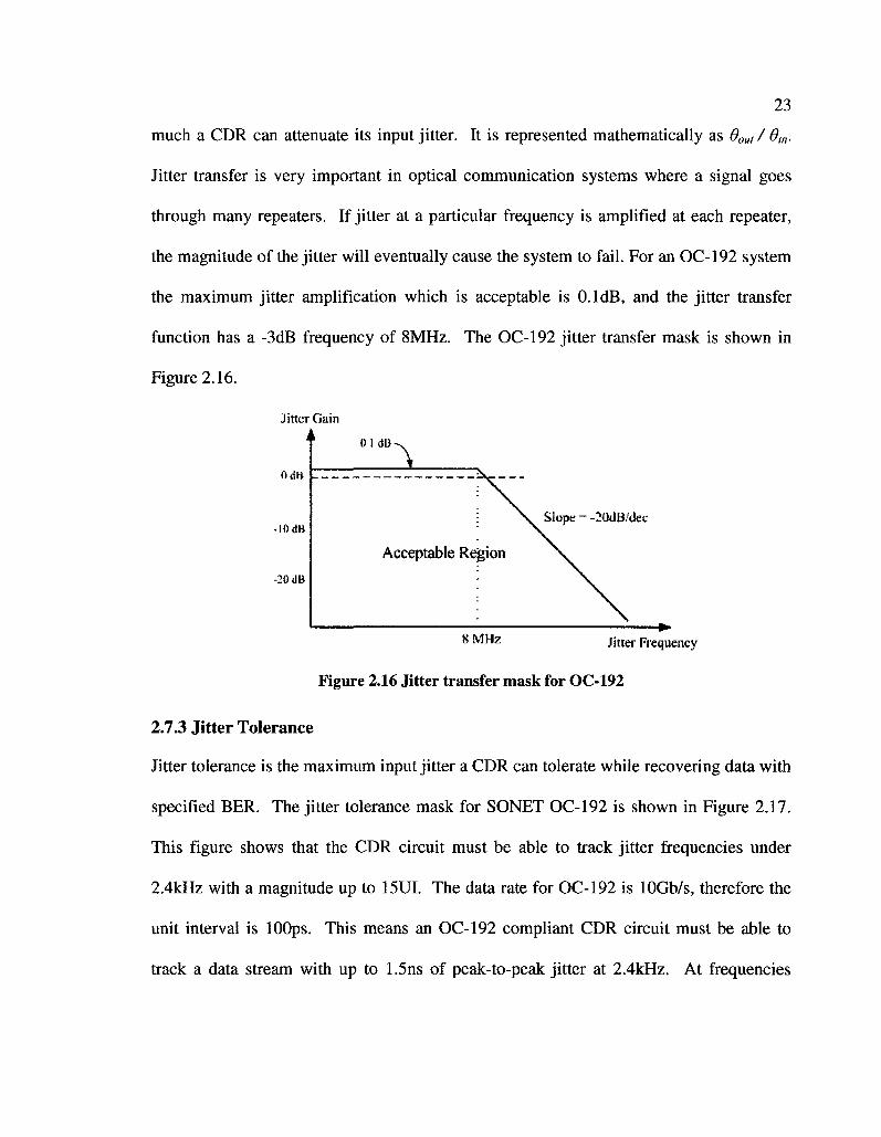
23
much a CDR can attenuate its input jitter. It is represented mathematically as 60ut/ 6in.
Jitter transfer is very important in optical communication systems where a signal goes
through many repeaters. If jitter at a particular frequency is amplified at each repeater,
the magnitude of the jitter will eventually cause the system to fail. For an OC-192 system
the maximum jitter amplification which is acceptable is O.ldB, and the jitter transfer
function has a -3dB frequency of 8MHz. The OC-192 jitter transfer mask is shown in
Figure 2.16.
jitter Gain
-IftdB
-20 JB
8 MHz jj( t e r pj-equency
Figure 2.16 Jitter transfer mask for OC-192
2.7.3 Jitter Tolerance
Jitter tolerance is the maximum input jitter a CDR can tolerate while recovering data with
specified BER. The jitter tolerance mask for SONET OC-192 is shown in Figure 2.17.
This figure shows that the CDR circuit must be able to track jitter frequencies under
2.4kHz with a magnitude up to 15UI. The data rate for OC-192 is lOGb/s, therefore the
unit interval is lOOps. This means an OC-192 compliant CDR circuit must be able to
track a data stream with up to 1.5ns of peak-to-peak jitter at 2.4kHz. At frequencies
L o i m -.
Acceptable Region
v Slope - -20dB/dec
+>
24
higher than 2.4kHz, the mask drops by two orders of magnitude in two discrete steps. At
jitter frequencies greater than 4MHz the CDR circuit must track only as long as the jitter
magnitude is less than 0.15UI, or 15ps peak-to-peak.
The maximum phase error which can be tolerated in any situation is equal to half the
period, or 0.5UI. This is expressed mathematically as
0 m - Gout < 0.51//
Using the mathematical representation of jitter transfer, we can rewrite the above
equation as,
Bm(l-kSL')<0.5UI
0 m ( l - / r rems(s ) ) < 0.5///
8m< 05UI 2.1
Equation 2.1 describes a relationship where the input jitter 6tn must be less than the
expression on the right hand side. Since the maximum magnitude of input jitter is the
jitter tolerance, an expression for jitter tolerance can be written as,
J t o m = °™> 2.2 J v J 1-Jtrans(s)
Jitter tolerance and jitter transfer create some obvious design constraints for a CDR
circuit. The OC-192 jitter tolerance mask shows that the system must track jitter of
reasonably large magnitudes less than 4MHz. As a PLL tracks jitter at frequencies less
than its loop bandwidth, the loop bandwidth of an OC-192 CDR circuit must be greater
than 4MHz. The jitter transfer mask shows that the input jitter with magnitude greater
than 8MHz must be significantly attenuated. As a CDR circuit attenuates jitter at
25
frequencies greater than its loop bandwidth, the bandwidth must be less than 8MHz. For
this reason most CDR circuits for OC-192 application have a system bandwidth of
approximately 6MHz.
Input jitter Magnitude
L
\ . Acceptable Region
" r ^ i Y — — . - . . . „ — . . . » a [ i J
* ! > • * •
2 4 KHz 24 KHz 4 MHz j , t t e r
frequency
Figure 2.17 Jitter tolerance mask for OC-192
2.8 Modelling
One of the advantages of a linear phase detector is the ease of analysis. The analysis is
based on the classical loop theory of PLL and is therefore used for the derivation of jitter
transfer and jitter tolerance. On the other hand, a bang-bang phase detector is very
challenging to analyze because of its non linear behaviour. While the output of a linear
phase detector is proportional to the phase error, the output of a bang-bang phase detector
is either UP or DOWN, regardless of the magnitude of the phase error.
In recent years, a number of papers have been published describing models for the
analysis of the nonlinear behaviour of the bang-bang phase detector. Reviewing most of
the papers, there are two main methods for analyzing the bang-bang PLL loop. The first
26
method was introduced by Walker [1] and the second method was illustrated by Lee et al.
[29]. In sections 2.8.1 and 2.8.2 we will discuss each method into more details.
Other methods have been utilized to analyze the nonlinear loop dynamics [30-34]. In
[30, 31] analysis of first and second order bang-bang PLL loops were analyzed using a
discrete-time iterative method. The work was focused on studying the loop stability by
investigating limit cycles. A continuation of this work was presented in [32] for third
order bang-bang CDR circuits using discrete-time and continuous-time analysis.
Equations were derived to describe the steady-state solutions and stability of the loop was
illustrated.
Statistical analysis of first order bang-bang CDR circuit was used in [33] to analyze
the steady-state timing jitter. An analogy was made between first order delta modulator
and bang-bang CDR circuit in order to relate hunting jitter and slew rate limiting in bang-
bang PLL loop to granular noise and slope overload in a delta modulator. However, jitter
transfer and jitter tolerance analyses were not discussed in this paper.
Describing functions method was used in [34] for jitter tolerance analysis. However,
the analysis is not accurate and there was no closed form solution for the jitter tolerance
expression.
2.8.1 Analysis of bang-bang PLL loop: method 1
Walker was the first one to explain the influence of the non linear behaviour on the loop
dynamics for the first and second order bang-bang CDR circuits [4]. Walker analyzed
the first order loop by modelling the bang-bang phase detector with a binary quantizer as
shown in figure 2.18. The binary quantizer limits the phase error of the loop at each
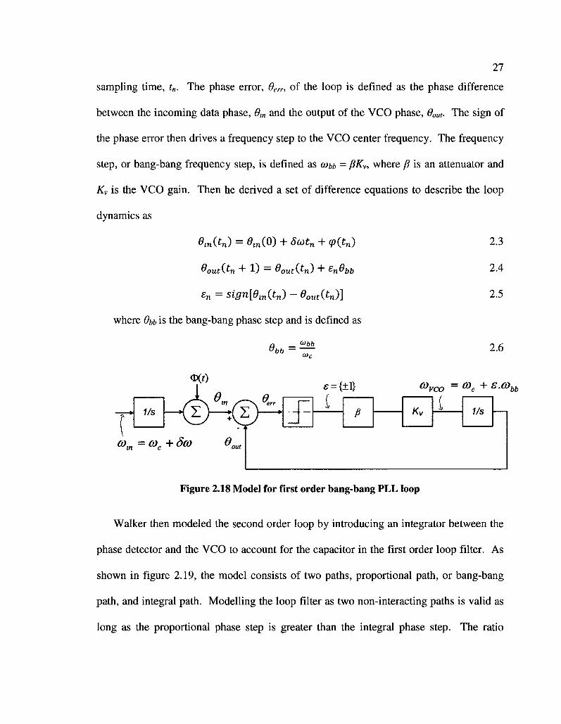
27
sampling time, t„. The phase error, 6err, of the loop is defined as the phase difference
between the incoming data phase, 6in and the output of the VCO phase, 60ut. The sign of
the phase error then drives a frequency step to the VCO center frequency. The frequency
step, or bang-bang frequency step, is defined as oibb = 0Kv, where /? is an attenuator and
Kv is the VCO gain. Then he derived a set of difference equations to describe the loop
dynamics as
Qm(tn) = 0in(O) + 8a)tn + <p(tn) 2.3
9out(tn + 1) = # o u t ( t n ) + £n9bb 2.4
£n = sign&nttn) - eout(tn)] 2.5
where 8bb is the bang-bang phase step and is defined as
n _ °>bb 2.6
°>m =0)c+8(0
<°VCO =G>c+ £°>bb
Figure 2.18 Model for first order bang-bang PLL loop
Walker then modeled the second order loop by introducing an integrator between the
phase detector and the VCO to account for the capacitor in the first order loop filter. As
shown in figure 2.19, the model consists of two paths, proportional path, or bang-bang
path, and integral path. Modelling the loop filter as two non-interacting paths is valid as
long as the proportional phase step is greater than the integral phase step. The ratio
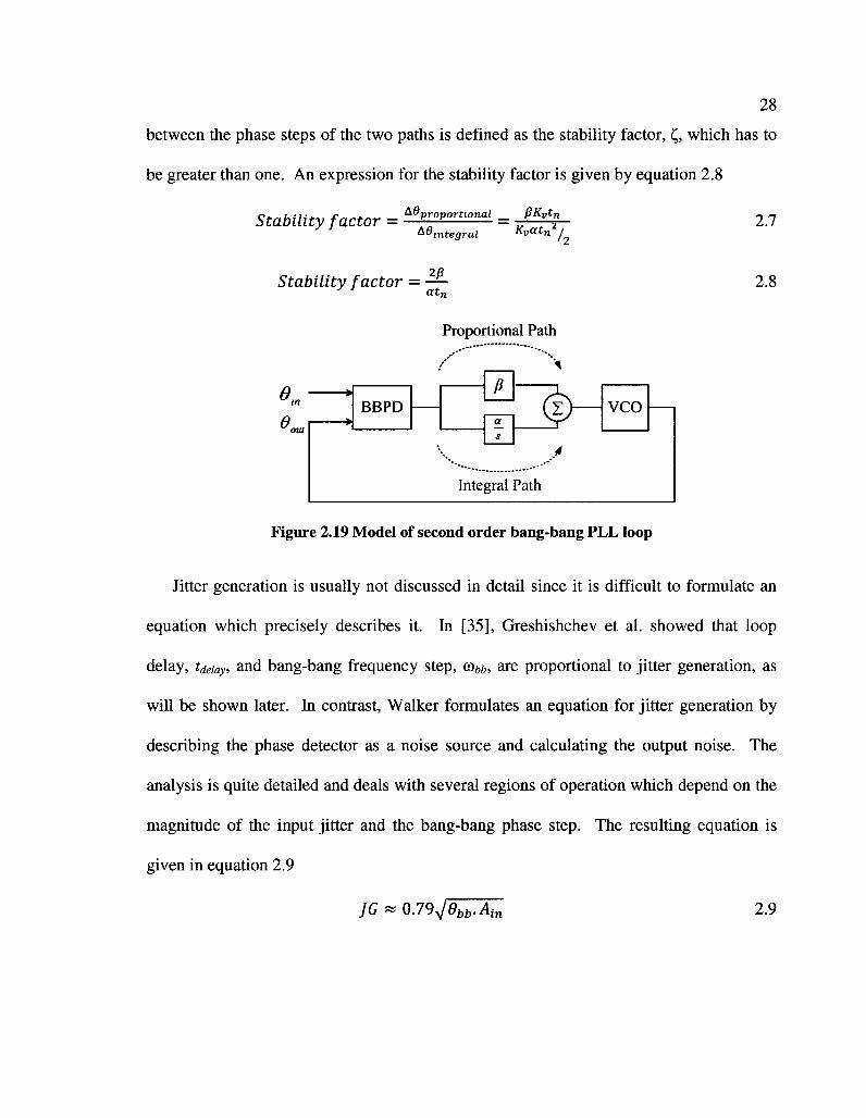
28
between the phase steps of the two paths is defined as the stability factor, £, which has to
be greater than one. An expression for the stability factor is given by equation 2.8
2.7 Stability factor = AVoPom0nai = JK^_ ^integral Hvatn j
26
Stability factor = -J-atn
Proportional Path
e e
in BBPD
\s
P
a s
\
A-4
Integral Path
VCO
Figure 2.19 Model of second order bang-bang PLL loop
2.8
Jitter generation is usually not discussed in detail since it is difficult to formulate an
equation which precisely describes it. In [35], Greshishchev et al. showed that loop
delay, tdelay, and bang-bang frequency step, co ,, are proportional to jitter generation, as
will be shown later. In contrast, Walker formulates an equation for jitter generation by
describing the phase detector as a noise source and calculating the output noise. The
analysis is quite detailed and deals with several regions of operation which depend on the
magnitude of the input jitter and the bang-bang phase step. The resulting equation is
given in equation 2.9
]G * 0.79VObb-Atn 2.9
29
In chapters 3 and 4 we will discuss Walker's analysis for jitter transfer and jitter tolerance
respectively.
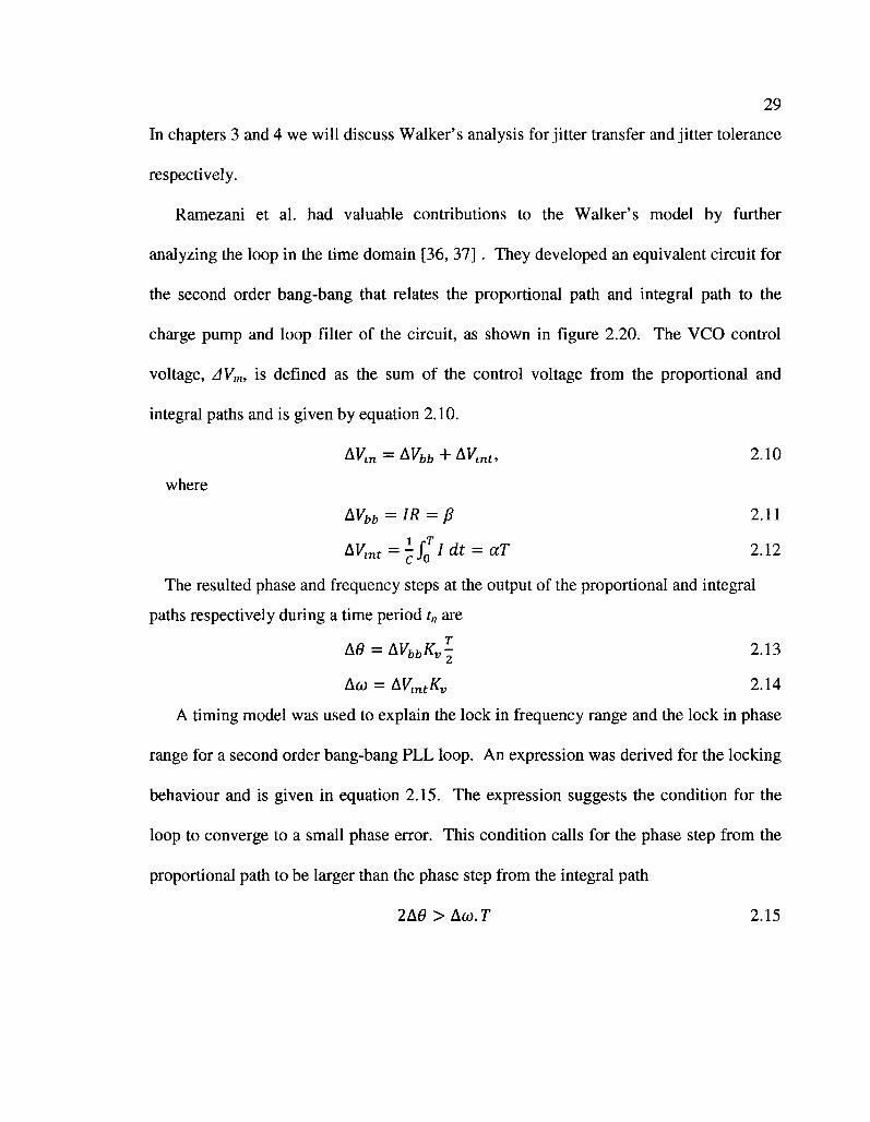
Ramezani et al. had valuable contributions to the Walker's model by further
analyzing the loop in the time domain [36, 37] . They developed an equivalent circuit for
the second order bang-bang that relates the proportional path and integral path to the
charge pump and loop filter of the circuit, as shown in figure 2.20. The VCO control
voltage, AVm, is defined as the sum of the control voltage from the proportional and
integral paths and is given by equation 2.10.
AVin = AVbb + AVint, 2.10
where
AVbb=IR = B 2.11
AVint=-JTQldt = aT 2.12
The resulted phase and frequency steps at the output of the proportional and integral
paths respectively during a time period tn are
L9 = WbbKv\ 2.13
A(o = AVintKv 2.14
A timing model was used to explain the lock in frequency range and the lock in phase
range for a second order bang-bang PLL loop. An expression was derived for the locking
behaviour and is given in equation 2.15. The expression suggests the condition for the
loop to converge to a small phase error. This condition calls for the phase step from the
proportional path to be larger than the phase step from the integral path
2A6>A(O.T 2.15
30
Looking at equations 2.11, 2.12, 2.13 and 2.14, it becomes evident that equation 2.15 is
the same expression as the stability factor that Walker introduced and is shown in
equation 2.8.
B>aT 2.16
Although Ramezani et al. discussed in more details the loop dynamics of second order
bang-bang CDR circuit, they did not analyze jitter transfer and jitter tolerance.
Q i
AV„
Figure 2.20 Charge pump and loop filter equivalent circuit
Greshishev et al. used Walker's model for the second order circuit to design a lOGb/s
bang-bang receiver [35]. He used the model to make an analogy with the behaviour of a
double integration delta modulator with prediction [38] to approximate the bang-bang
frequency step, cobb- Based on the delta modulator, he showed a relationship between the
jitter transfer bandwidth, co}, and the bang-bang frequency step, cobb, as in equation 2.17.
co, oc <*bb
J A, 2.17
where coj is the jitter transfer bandwidth, Ain is the jitter amplitude, cobb is the bang-bang
frequency step. Then he examines the effect of the bang-bang frequency step, a>bb, on the
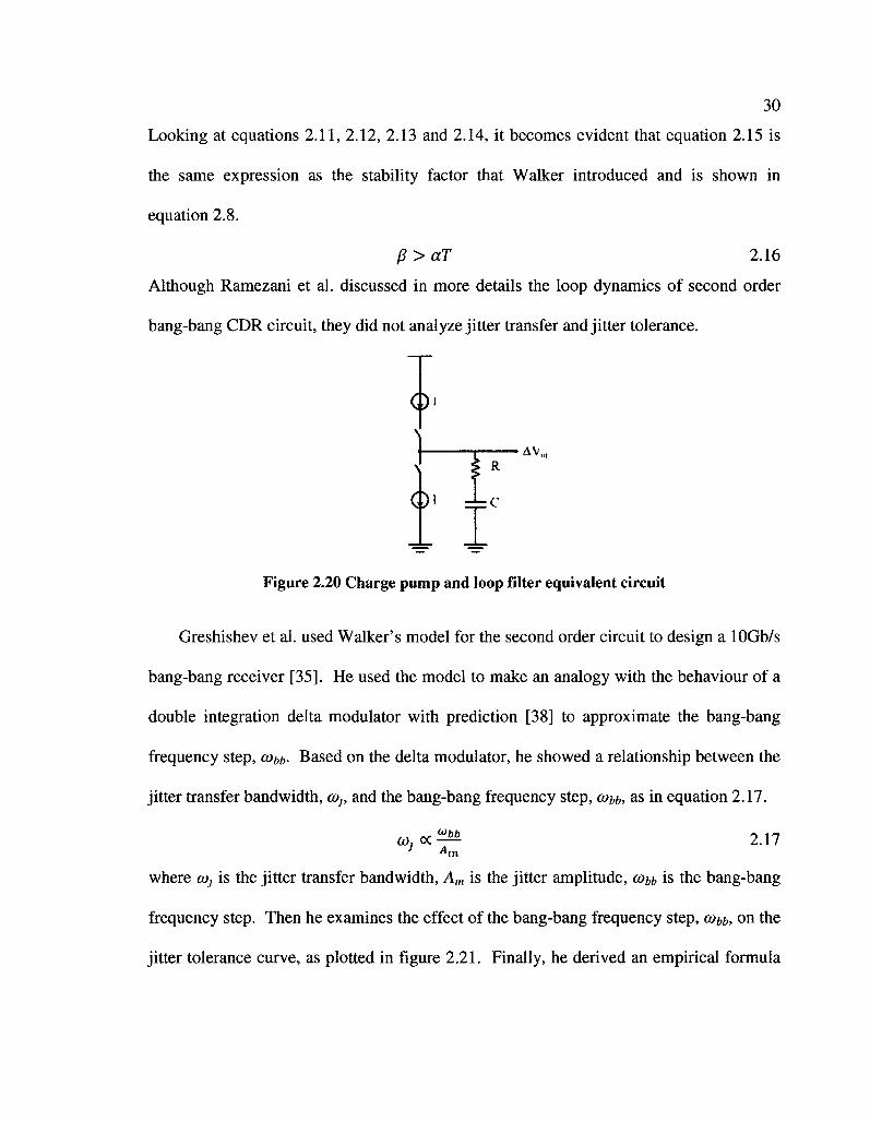
jitter tolerance curve, as plotted in figure 2.21. Finally, he derived an empirical formula
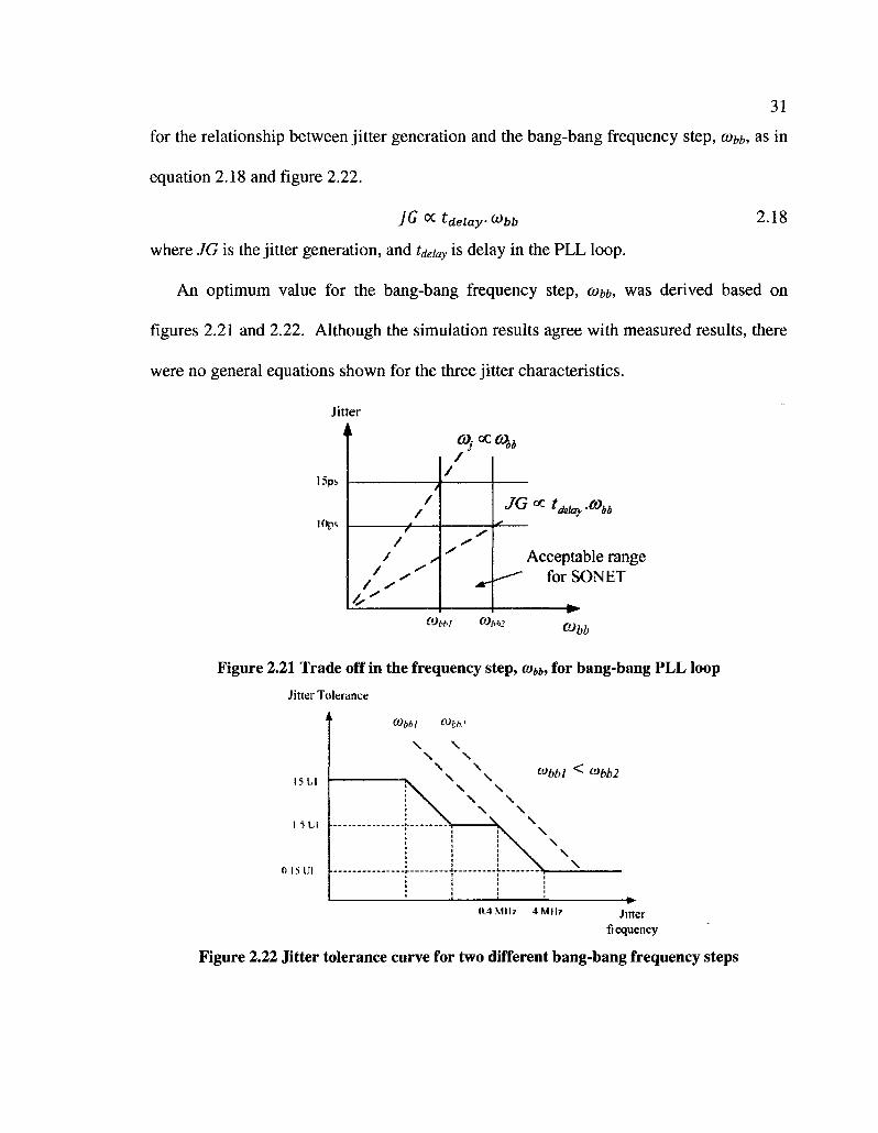
31
for the relationship between jitter generation and the bang-bang frequency step, cobb, as in
equation 2.18 and figure 2.22.
JG OC tdelay ^bb 2.18
where JG is the jitter generation, and tdeiay is delay in the PLL loop.
An optimum value for the bang-bang frequency step, cobb, was derived based on
figures 2.21 and 2.22. Although the simulation results agree with measured results, there
were no general equations shown for the three jitter characteristics.
Jitter
n
15pt
10p< /
/
4,"
fljQCfifc
J G | Q C * * * * • & »
Acceptable range for SONET
(Ot,t>! 0)1,1,2 OJbb
Figure 2.21 Trade off in the frequency step, (obb, for bang-bang PLL loop Jitter Tolerance
15 LI
1 5 UI
0 15UI
<»bbl ^ <»bb2
0.4 Mil? 4 Mil? Jitter frequency
Figure 2.22 Jitter tolerance curve for two different bang-bang frequency steps
32
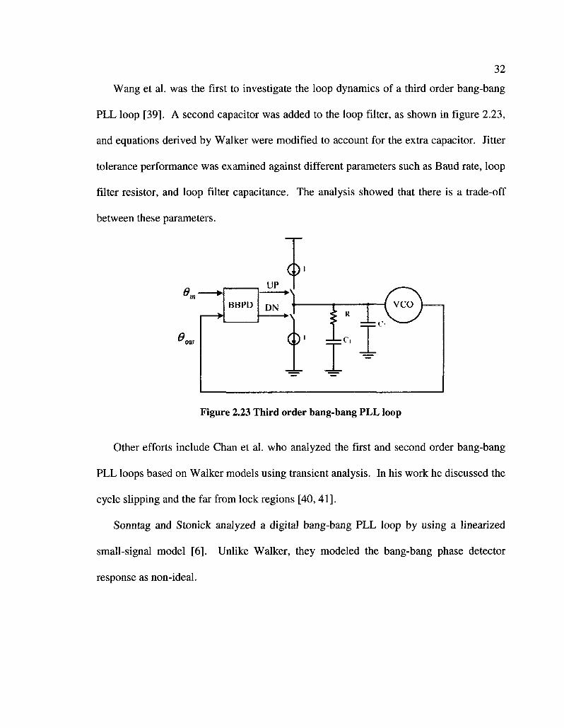
Wang et al. was the first to investigate the loop dynamics of a third order bang-bang
PLL loop [39]. A second capacitor was added to the loop filter, as shown in figure 2.23,
and equations derived by Walker were modified to account for the extra capacitor. Jitter
tolerance performance was examined against different parameters such as Baud rate, loop
filter resistor, and loop filter capacitance. The analysis showed that there is a trade-off
between these parameters.
e„
O
f?„
• BBPD
UP *)
DN
( ) '
-=-
r-
< R
= r,
-=-
— i
_!_
^ \ VCO ) . O
Figure 2.23 Third order bang-bang PLL loop
Other efforts include Chan et al. who analyzed the first and second order bang-bang
PLL loops based on Walker models using transient analysis. In his work he discussed the
cycle slipping and the far from lock regions [40,41].
Sonntag and Stonick analyzed a digital bang-bang PLL loop by using a linearized
small-signal model [6]. Unlike Walker, they modeled the bang-bang phase detector
response as non-ideal.
33
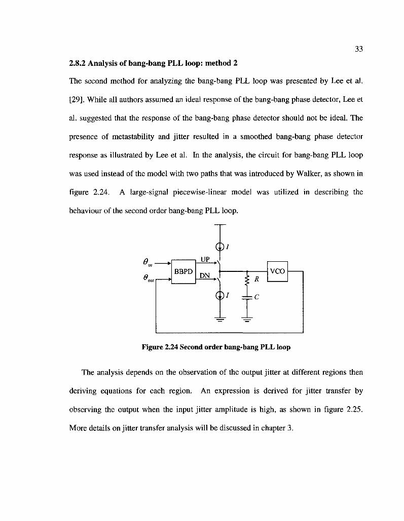
2.8.2 Analysis of bang-bang PLL loop: method 2
The second method for analyzing the bang-bang PLL loop was presented by Lee et al.
[29]. While all authors assumed an ideal response of the bang-bang phase detector, Lee et
al. suggested that the response of the bang-bang phase detector should not be ideal. The
presence of metastability and jitter resulted in a smoothed bang-bang phase detector
response as illustrated by Lee et al. In the analysis, the circuit for bang-bang PLL loop
was used instead of the model with two paths that was introduced by Walker, as shown in
figure 2.24. A large-signal piecewise-linear model was utilized in describing the
behaviour of the second order bang-bang PLL loop.
0..
e„ BBPD
UP
Qi
• \
DN
Q /
R
C
VCO
Figure 2.24 Second order bang-bang PLL loop
The analysis depends on the observation of the output jitter at different regions then
deriving equations for each region. An expression is derived for jitter transfer by
observing the output when the input jitter amplitude is high, as shown in figure 2.25.
More details on jitter transfer analysis will be discussed in chapter 3.
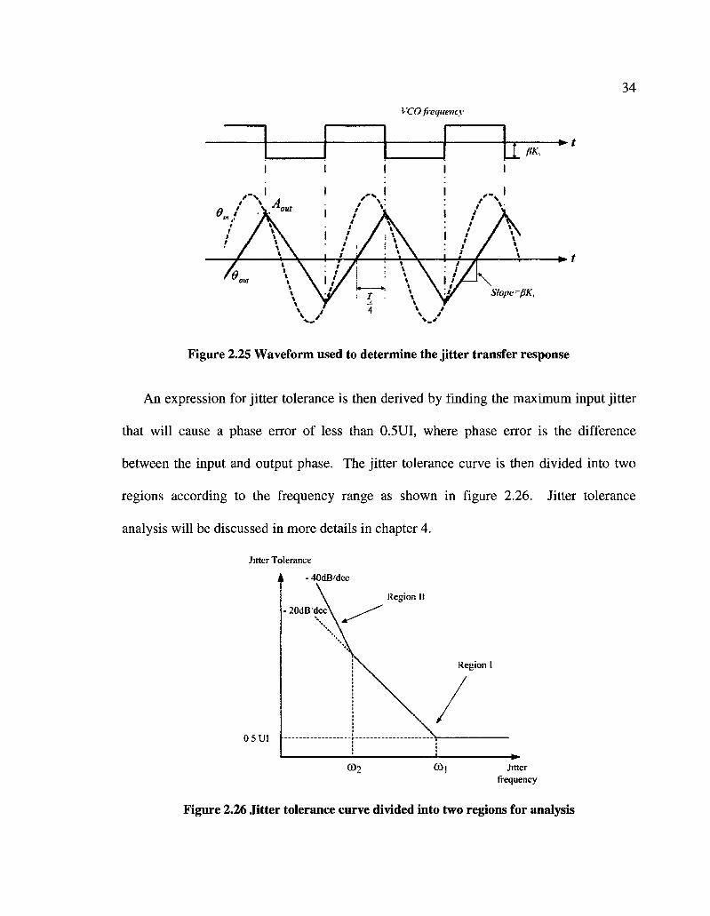
34
VCO frequency
Figure 2.25 Waveform used to determine the jitter transfer response
An expression for jitter tolerance is then derived by finding the maximum input jitter
that will cause a phase error of less than 0.5UI, where phase error is the difference
between the input and output phase. The jitter tolerance curve is then divided into two
regions according to the frequency range as shown in figure 2.26. Jitter tolerance
analysis will be discussed in more details in chapter 4.
Jitter Tolerance
- 40dB'dcc
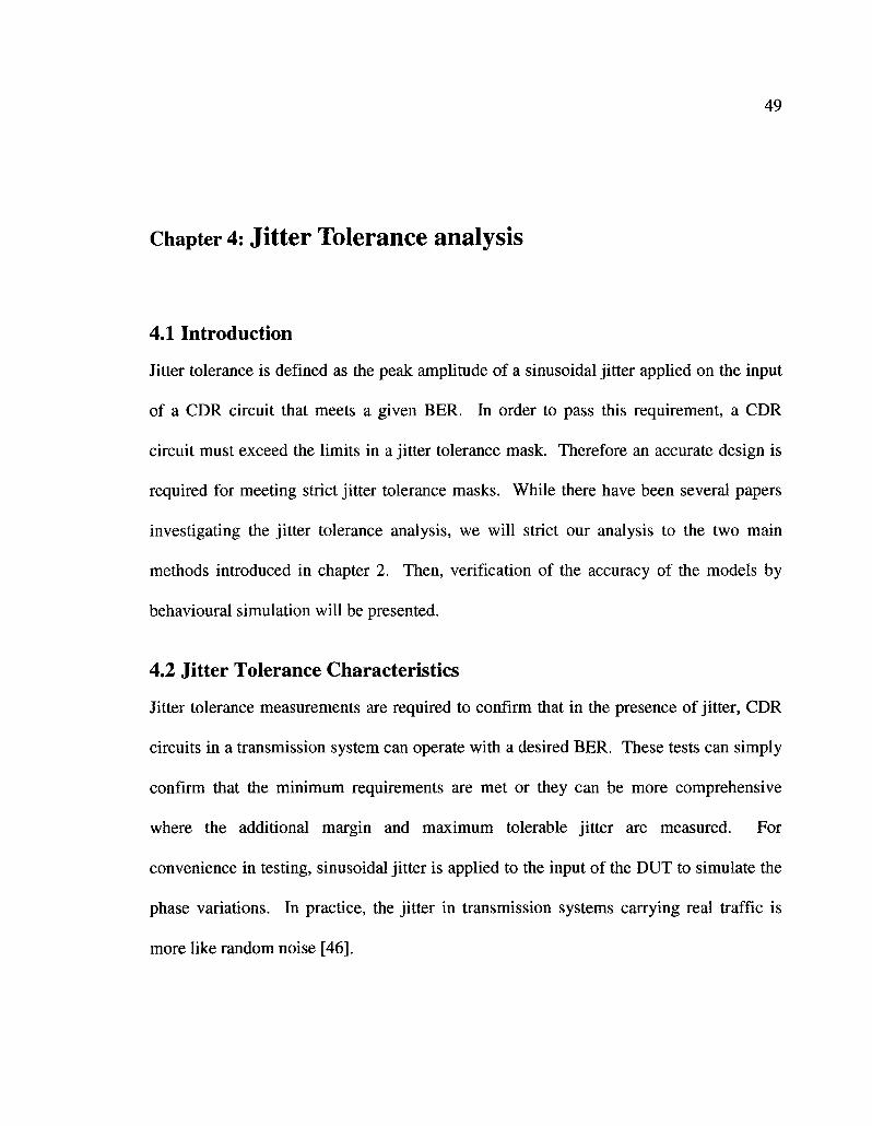
Region II
Region I
OS US
Jitter frequency
Figure 2.26 Jitter tolerance curve divided into two regions for analysis
35
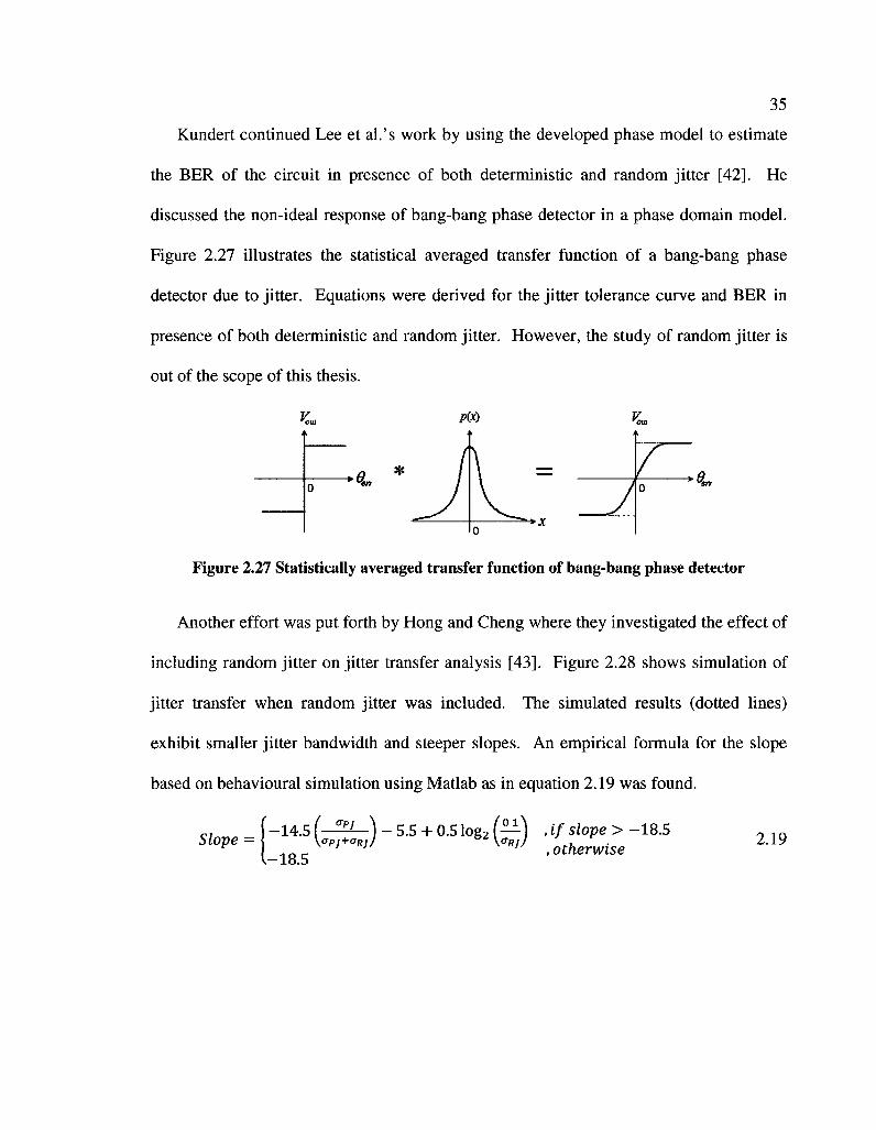
Kundert continued Lee et al.'s work by using the developed phase model to estimate
the BER of the circuit in presence of both deterministic and random jitter [42]. He
discussed the non-ideal response of bang-bang phase detector in a phase domain model.
Figure 2.27 illustrates the statistical averaged transfer function of a bang-bang phase
detector due to jitter. Equations were derived for the jitter tolerance curve and BER in
presence of both deterministic and random jitter. However, the study of random jitter is
out of the scope of this thesis.
v ' O B I
- &
Figure 2.27 Statistically averaged transfer function of bang-bang phase detector
Another effort was put forth by Hong and Cheng where they investigated the effect of
including random jitter on jitter transfer analysis [43]. Figure 2.28 shows simulation of
jitter transfer when random jitter was included. The simulated results (dotted lines)
exhibit smaller jitter bandwidth and steeper slopes. An empirical formula for the slope
based on behavioural simulation using Matlab as in equation 2.19 was found.
c . (-14.5 f - ^ - ) - 5 . 5 +0.5 log2f—) , if slope > -18.5 (-18 5 .otherwise
2.19
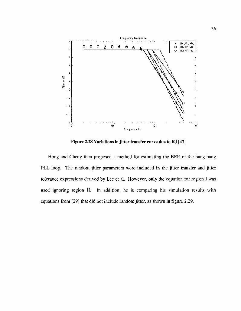
36
rrv^imnrv Ro;|irin = e
U •
fi -•n
- 'b
>d
ft a ft a 6 » » A |
10 l--e quern. . H -
Figure 2.28 Variations in jitter transfer curve due to RJ [43]
Hong and Cheng then proposed a method for estimating the BER of the bang-bang
PLL loop. The random jitter parameters were included in the jitter transfer and jitter
tolerance expressions derived by Lee et al. However, only the equation for region I was
used ignoring region II. In addition, he is comparing his simulation results with
equations from [29] that did not include random jitter, as shown in figure 2.29.
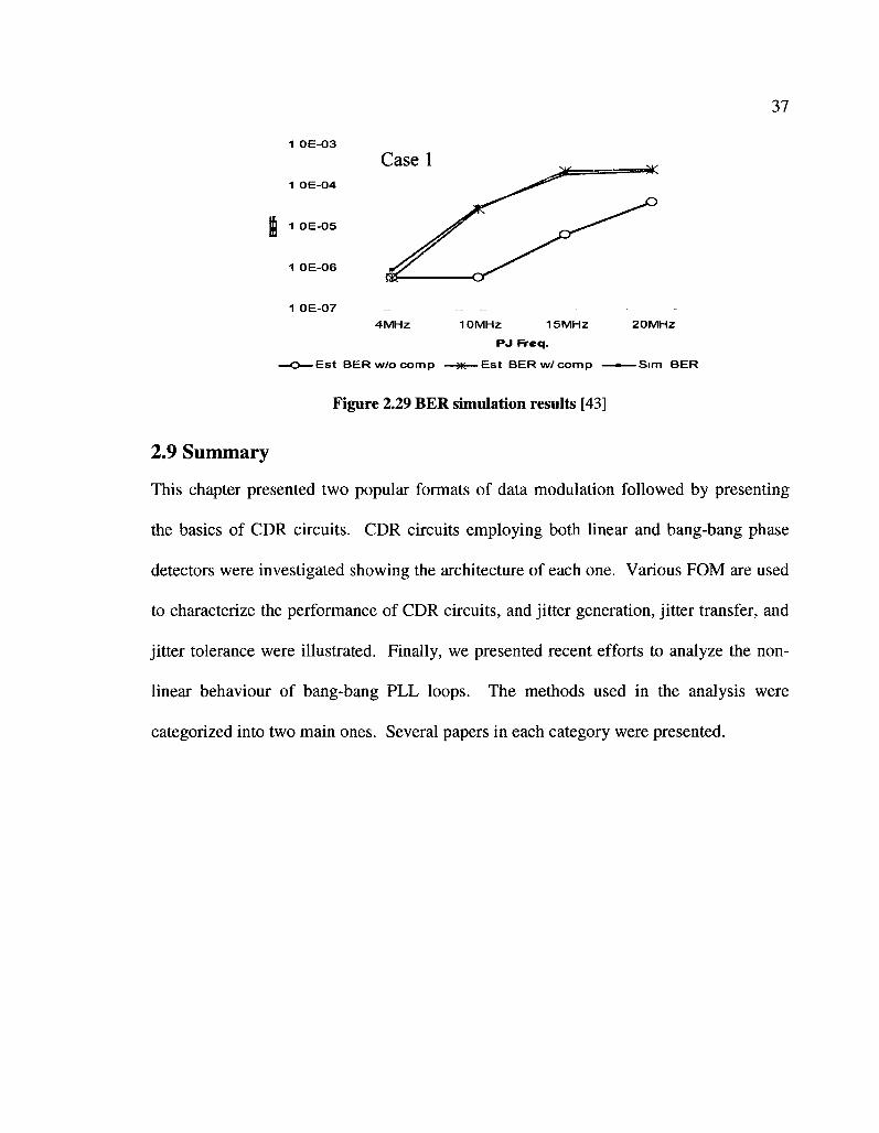
37
1 oe-03
1 OE-04
I 1 OE-05
1 OE-06
1 OE-07
4MHz 10MHz 15MHz 20MHz
PJ i=req.
—O—Est BERw/ocomp —m—Est B E R w / c o m p — • — S i m BER
Figure 2.29 BER simulation results [43]
2.9 Summary
This chapter presented two popular formats of data modulation followed by presenting
the basics of CDR circuits. CDR circuits employing both linear and bang-bang phase
detectors were investigated showing the architecture of each one. Various FOM are used
to characterize the performance of CDR circuits, and jitter generation, jitter transfer, and
jitter tolerance were illustrated. Finally, we presented recent efforts to analyze the non
linear behaviour of bang-bang PLL loops. The methods used in the analysis were
categorized into two main ones. Several papers in each category were presented.
mi y
38
Chapter 3: Jitter Transfer analysis
3.1 Introduction
Jitter transfer function is referred to as the ratio of the output jitter to the jitter applied at
the input versus frequency. In long haul transmission systems where repeaters exist, it is
very important to ensure that the CDR circuit meets the jitter transfer mask requirements.
Several methods have been proposed for analyzing the nonlinear behaviour of BBPDs
[1,29,37,44]. We have shown in section 2.8 that there are two main methods for
analyzing second order bang-bang PLL loop. In this chapter we will use both methods to
analyze the jitter transfer characteristics for the second order bang-bang PLL loop. A
more accurate expression is proposed and verified by simulation [45].
3.2 Jitter Transfer Characteristics
As defined in section 2.7.2, Jitter transfer is the relationship between the applied input
jitter and the resulting output jitter as a function of frequency. It is a measure of how
much jitter is attenuated or amplified from the input to the output of a network
equipment. If the jitter transfer mask is met, then there is no amplification of jitter by the
network equipment as that jitter traverses multiple repeaters.
To measure jitter transfer, the amplitude of the output jitter is compared to the
amplitude of the input jitter, as shown in figure 3.1 [46]. According to the jitter transfer
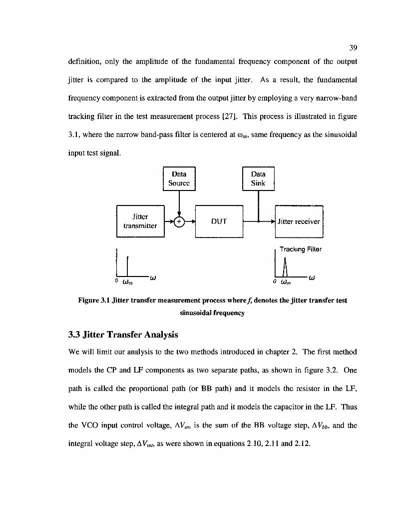
39
definition, only the amplitude of the fundamental frequency component of the output
jitter is compared to the amplitude of the input jitter. As a result, the fundamental
frequency component is extracted from the output jitter by employing a very narrow-band
tracking filter in the test measurement process [27]. This process is illustrated in figure
3.1, where the narrow band-pass filter is centered at oo„„ same frequency as the sinusoidal
input test signal.
Jitter transmitter
Data Source
< <
"KLJ ' DUT
Data ; Sink
Jitter receiver
0 (Jj„ "UJ
Tracking Filter
i 0 U)„
U)
Figure 3.1 Jitter transfer measurement process where/, denotes the jitter transfer test
sinusoidal frequency
3.3 Jitter Transfer Analysis
We will limit our analysis to the two methods introduced in chapter 2. The first method
models the CP and LF components as two separate paths, as shown in figure 3.2. One
path is called the proportional path (or BB path) and it models the resistor in the LF,
while the other path is called the integral path and it models the capacitor in the LF. Thus
the VCO input control voltage, AV,„, is the sum of the BB voltage step, AVbb, and the
integral voltage step, AVmt, as were shown in equations 2.10, 2.11 and 2.12.
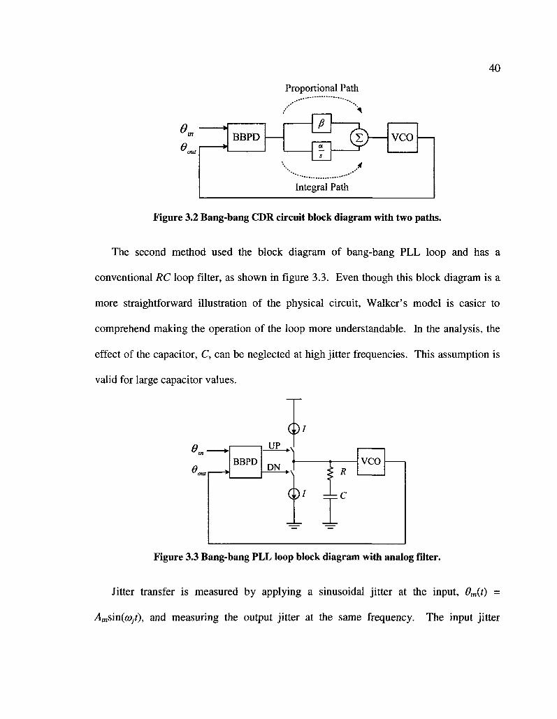
40
Proportional Path
0 e
1 » m
1 * BBPD
>
n ^ s
4
Integral Path
VCO
Figure 3.2 Bang-bang CDR circuit block diagram with two paths.
The second method used the block diagram of bang-bang PLL loop and has a
conventional RC loop filter, as shown in figure 3.3. Even though this block diagram is a
more straightforward illustration of the physical circuit, Walker's model is easier to
comprehend making the operation of the loop more understandable. In the analysis, the
effect of the capacitor, C, can be neglected at high jitter frequencies. This assumption is
valid for large capacitor values.
0U
0„ BBPD
UP
Qr
+ \
DN *\
( ) / =L
R
C
VCO
Figure 3.3 Bang-bang PLL loop block diagram with analog filter.
Jitter transfer is measured by applying a sinusoidal jitter at the input, 0m(t) =
Ainsm(a)jt), and measuring the output jitter at the same frequency. The input jitter
41
amplitude is specified according to the jitter tolerance mask. At low frequencies the
bang-bang loop can track the input jitter, and the gain is close to zero dB. As the jitter
frequency increases, the loop cannot track the input and the phase error (8err = 0in - 0out)
increases. The region where the loop tracks is represented by the horizontal line on the
jitter transfer curve in figure 2.16. The -20dB/dec slope is where the loop is slewing
resulting in large errors. The corner frequency, which differentiates these two regions, is
called the -3dB bandwidth (corner frequency) of the jitter transfer, ©_3dB-
We will start presenting the analysis for Walker first in section 3.3.1, following the
analysis by Lee et al. in section 3.3.2. However, in the analysis of both representations,
the jitter transfer definition was disregarded leading to inaccurate results. Consequently,
we had to apply the jitter transfer definition to derive a more accurate expression.
3.3.1 Method 1
Walker made a useful analogy between the bang-bang PLL loop and the Delta Modulator
(DM) that allowed a valid explanation of the loop using existing theory on DM. In the
DM, two types of distortion exist: quantization distortion (granular noise) and slope
overload distortion. If the DM output is able to track the sinusoidal input signal, there is
no error and the quantizer output frequently changes its sign. This tracking behaviour
can be seen in figure 3.4 (a). If, on the other hand, the DM output is unable to follow the
sinusoidal input signal shape, errors start to occur and the loop is said to experience slope
overload [38], as shown in figure 3.4(b).
42
Figure 3.4 Slewing mechanism in PLL loop: (a) Onset of slewing, (b) Heavy slewing: loop
cannot track the input sinusoidal shape.
Slewing, which occurs on the jitter transfer curve, is the same phenomena as slope
overload in DM. This analogy enables us to derive an expression for the slewing
condition based on DM theory.
For a sinusoidal input signal with amplitude Ain and frequency co}, the slope of the
input signal is
9'in(t) = Ain.a)j.cos ((Ojt). 3.1
As mentioned earlier, the integral path is neglected reducing the loop to a first order loop.
The maximum rate of increase of 60ut(t) is equal to the proportional path gain. Thus,
e'outit) = BKV, 3.2
where Kv is the VCO gain in rad/V.s. Slope overload is avoided if 9'm < 6'0lU , and
therefore from 3.1 and 3.2:
Aina)j < BKV. 3.3
The amplitude-frequency product defines the condition, so as to avoid slope overload.
The loop starts to overload when either the amplitude or the frequency increases. Thus,
43
the maximum input jitter frequency where the loop can track the input jitter can be
expressed as:
0)W = — . 3.4 "in
In this expression, the maximum input jitter frequency is inversely proportional to the
jitter amplitude, cow can be thought of as the corner frequency for the CDR circuit as in a
linear model. In other words, using this bandwidth will ensure that the CDR circuit never
slews.
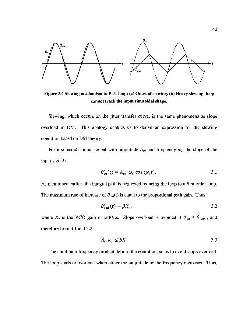
3.3.2 Method 2
Sinusoidal jitter with specified amplitude is applied to the block diagram in figure 3.3,
and the frequency is increased until slewing occurs. To analyze the jitter transfer we use
figure 3.5 as an extreme case where the bang-bang PLL loop is slewing. The output jitter
is a triangular waveform with amplitude Aout and frequency coj. We can find the output
jitter's peak amplitude by a simple integration of the slope for a duration of 7}/2 (7} =
2ji/fflj), that is,
A - ^ 35 Mout — 4 • J - J
Therefore, the jitter transfer function can be represented as
\Aout\ _ n/3Kv _ , I Aln I 2/lmo),
VCO frequency
Figure 3.5 CDR loop is slewing.
44
+>t
+-t
This expression shows the dependency of the jitter transfer on the input jitter
amplitude Aw. This dependency explains why the loop bandwidth of bang-bang PLL
loops cannot be defined in a strict sense. An approximate value for the maximum
frequency of the triangular waveform when Aout = Ain can be found as:
npKv COL =
2A, 3.7
3.3.3 Proposed expression
In order to comply with the definition, the output jitter must be measured at the same
frequency as the input jitter. Consequently, we expand the output waveform into its
Fourier series and measure the peak amplitude of the fundamental frequency component
only. Taking only the fundamental frequency component corresponds to the describing
function method used to analyze non linear systems [47]. For a triangle waveform the
Fourier expansion is as follows:
45
, , 8 1 1 fit) = —rfsincot — -sin3u>t + —sin5cot — )
n* 9 25
Thus, the jitter transfer function in equation 3.7 can be modified to be
Equation 3.8 gives the -3dB bandwidth of the jitter transfer curve when both input
and output jitter amplitudes are measured at the same frequency. In our analysis we use
the physical output waveforms from simulation results to derive the jitter transfer
expression.
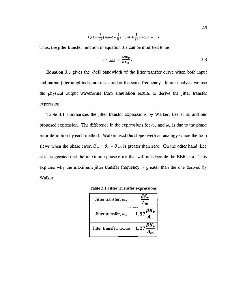
Table 3.1 summarizes the jitter transfer expressions by Walker, Lee et al. and our
proposed expression. The difference in the expressions for cow and coL is due to the phase
error definition by each method. Walker used the slope overload analogy where the loop
slews when the phase error, 6err = 9m - Bout, is greater than zero. On the other hand, Lee
et al. suggested that the maximum phase error that will not degrade the BER is n. This
explains why the maximum jitter transfer frequency is greater than the one derived by
Walker.
Table 3.1 Jitter Transfer expressions
Jitter transfer, cow
Jitter transfer, COL
Jitter transfer, co.sdB
PKV
"•in
1 . 5 7 ^ A in
1 . 2 7 ^ Ain
46
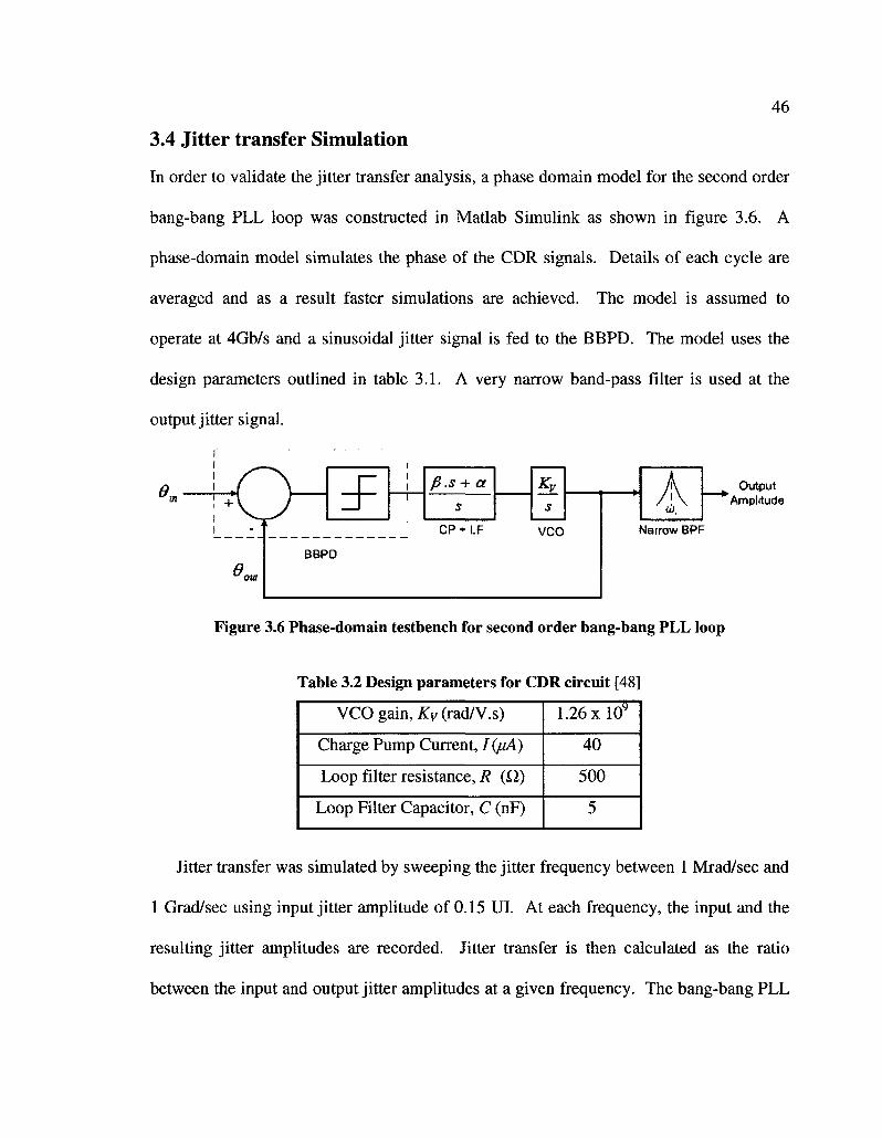
3.4 Jitter transfer Simulation
In order to validate the jitter transfer analysis, a phase domain model for the second order
bang-bang PLL loop was constructed in Matlab Simulink as shown in figure 3.6. A
phase-domain model simulates the phase of the CDR signals. Details of each cycle are
averaged and as a result faster simulations are achieved. The model is assumed to
operate at 4Gb/s and a sinusoidal jitter signal is fed to the BBPD. The model uses the
design parameters outlined in table 3.1. A very narrow band-pass filter is used at the
output jitter signal.
\f + \ , J
Gom
> \
zF i i i
BBPD
fi.s + a
s
CP * LF
s
VCO
A Narrow BPF
Figure 3.6 Phase-domain testbench for second order bang-bang PLL loop
Table 3.2 Design parameters for CDR circuit [48]
VCO gain, ^(rad/V.s)
Charge Pump Current, I(juA)
Loop filter resistance, R (Q.)
Loop Filter Capacitor, C (nF)
1.26 xlO9
40
500
5
Jitter transfer was simulated by sweeping the jitter frequency between 1 Mrad/sec and
1 Grad/sec using input jitter amplitude of 0.15 UI. At each frequency, the input and the
resulting jitter amplitudes are recorded. Jitter transfer is then calculated as the ratio
between the input and output jitter amplitudes at a given frequency. The bang-bang PLL
47
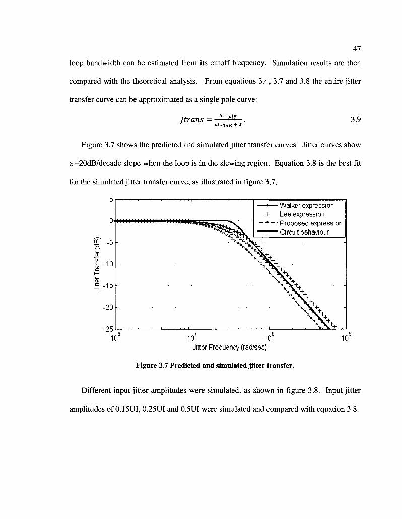
loop bandwidth can be estimated from its cutoff frequency. Simulation results are then
compared with the theoretical analysis. From equations 3.4, 3.7 and 3.8 the entire jitter
transfer curve can be approximated as a single pole curve:
W-3dB Jtrans =
U-3dB + s 3.9
Figure 3.7 shows the predicted and simulated jitter transfer curves. Jitter curves show
a -20dB/decade slope when the loop is in the slewing region. Equation 3.8 is the best fit
for the simulated jitter transfer curve, as illustrated in figure 3.7.
DO T>
l
<1> I I I C
m * H i
(l) e
=i
-in
-15
-20
-25
l l l l l l l t t t t l t t l l l l l i i i . i i i i n n
•*— Walker expression + Lee expression • * - - Proposed expression
Circuit behaviour
- I I I I—1—L
10 10 10" Jitter Frequency (rad/sec)
Figure 3.7 Predicted and simulated jitter transfer.
10
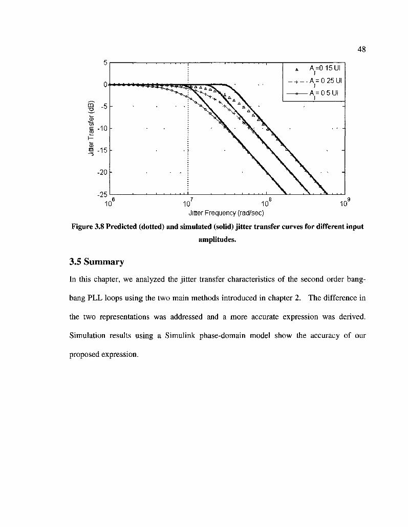
Different input jitter amplitudes were simulated, as shown in figure 3.8. Input jitter
amplitudes of 0.15UI, 0.25UI and 0.5UI were simulated and compared with equation 3.8.
48
0-
m o i
(i) fn
i
o> —D
S
-1U
-15
-20
-25
> » I n i | j »
A=0 15UI )
. A = 0 25 UI
5UI
10 10 10" Jitter Frequency (rad/sec)
10
Figure 3.8 Predicted (dotted) and simulated (solid) jitter transfer curves for different input
amplitudes.
3.5 Summary
In this chapter, we analyzed the jitter transfer characteristics of the second order bang-
bang PLL loops using the two main methods introduced in chapter 2. The difference in
the two representations was addressed and a more accurate expression was derived.
Simulation results using a Simulink phase-domain model show the accuracy of our
proposed expression.
49
Chapter 4: Jitter Tolerance analysis
4.1 Introduction
Jitter tolerance is defined as the peak amplitude of a sinusoidal jitter applied on the input
of a CDR circuit that meets a given BER. In order to pass this requirement, a CDR
circuit must exceed the limits in a jitter tolerance mask. Therefore an accurate design is
required for meeting strict jitter tolerance masks. While there have been several papers
investigating the jitter tolerance analysis, we will strict our analysis to the two main
methods introduced in chapter 2. Then, verification of the accuracy of the models by
behavioural simulation will be presented.
4.2 Jitter Tolerance Characteristics
Jitter tolerance measurements are required to confirm that in the presence of jitter, CDR
circuits in a transmission system can operate with a desired BER. These tests can simply
confirm that the minimum requirements are met or they can be more comprehensive
where the additional margin and maximum tolerable jitter are measured. For
convenience in testing, sinusoidal jitter is applied to the input of the DUT to simulate the
phase variations. In practice, the jitter in transmission systems carrying real traffic is
more like random noise [46].

50
A standard jitter tolerance mask is used as a reference during the test. A Sinusoidal
jitter, 0m(t) = A„,sin(cw/), is applied at the input of the DUT at a given frequency point. At
the receiver's end, a check for transmission errors is carried out and input jitter amplitude
is incremented or decremented until maximum tolerable jitter is determined. The process
is repeated for each frequency point until the jitter tolerance mask frequency range is
covered, as shown in figure 4.1. At low frequencies the bang-bang PLL loop can tolerate
more jitter and as a result the input jitter amplitude is expected to be large. As the jitter
frequency increases, the loop cannot tolerate much jitter and as a result there is a
limitation on the maximum tolerable input jitter. Jitter tolerance mask for OC-192 was
shown in chapter 2 and is presented here again for convenience.
Jitter sweep sequence through mask points with amplitude increment/decrement controlled by result
J
Measurement MTJ plot for DUT showing pass margin in excess of requirement
Jitter Amplitude
Jitter transmitter
DUT BER/Error receiver
r V Control ' algorithm
Jitter Frequency
Minimum DUT tolerance requirement. Not acceptable if below this line
Figure 4.1 Maximum tolerable jitter Test [46]
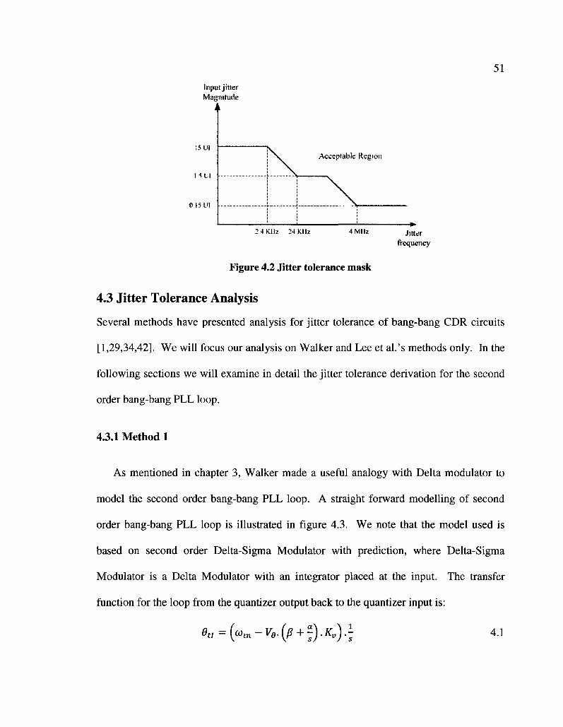
51 Input jitter Magnitude
i\
\ " • - " " -
7\ | '• * •
2 4Kllz 24 KHz 4 MHz j , t t e r
frequency
Figure 4.2 Jitter tolerance mask
4.3 Jitter Tolerance Analysis
Several methods have presented analysis for jitter tolerance of bang-bang CDR circuits
[1,29,34,42]. We will focus our analysis on Walker and Lee et al.'s methods only. In the
following sections we will examine in detail the jitter tolerance derivation for the second
order bang-bang PLL loop.
4.3.1 Method 1
As mentioned in chapter 3, Walker made a useful analogy with Delta modulator to
model the second order bang-bang PLL loop. A straight forward modelling of second
order bang-bang PLL loop is illustrated in figure 4.3. We note that the model used is
based on second order Delta-Sigma Modulator with prediction, where Delta-Sigma
Modulator is a Delta Modulator with an integrator placed at the input. The transfer
function for the loop from the quantizer output back to the quantizer input is:
Ot, = {o)in-Vg.(B+fj.Kv).^ 4.1
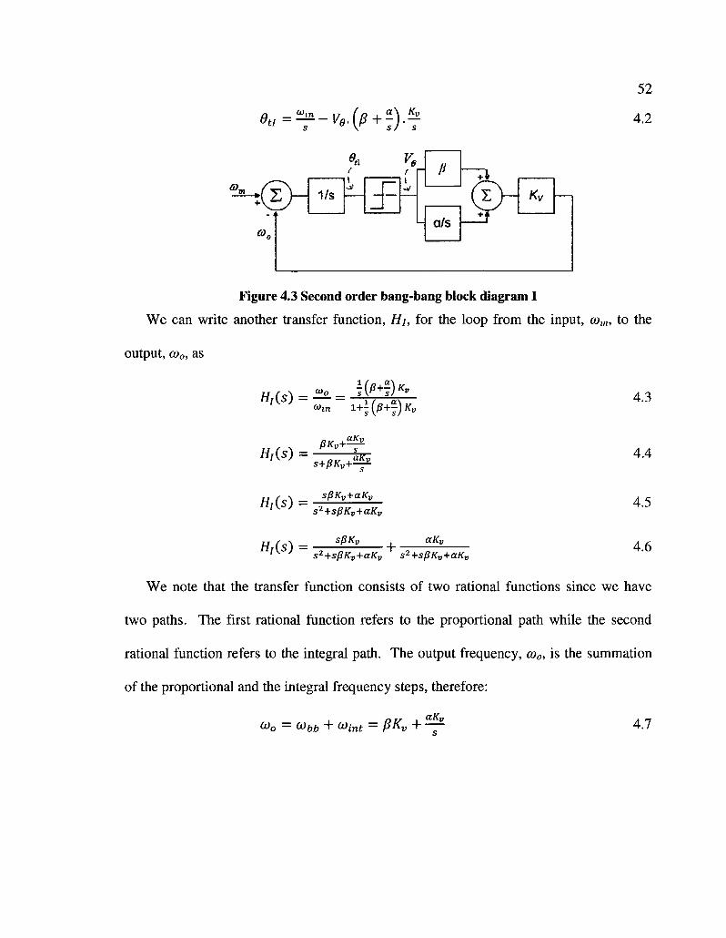
9tI=^-Ve.(B+^).Kf
52
4.2
6),.
& --'
®o
1/S ~J)
j ~
y9 i -
• j
- p +1
^ ^ - a/s
Kv
Figure 4.3 Second order bang-bang block diagram I
We can write another transfer function, Hi, for the loop from the input, com, to the
output, co0, as
4.3
4.4
4.5
4 6 " / v - " y s2+sfiKv+aKv ' s2+spKv+aKv
We note that the transfer function consists of two rational functions since we have
two paths. The first rational function refers to the proportional path while the second
rational function refers to the integral path. The output frequency, co0, is the summation
of the proportional and the integral frequency steps, therefore:
a0 = o)bb + a)int = BKv+-jL 4.7
tf/00 =
H7(s) =
/ / ,(*) =
W.fc^ -
PKV+^
sfiKv+aKv
s2+s/3Kv+aKv
spKv ccKv
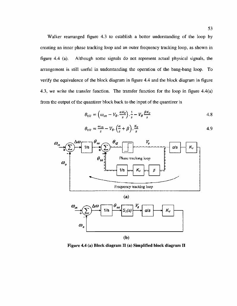
53
Walker rearranged figure 4.3 to establish a better understanding of the loop by
creating an inner phase tracking loop and an outer frequency tracking loop, as shown in
figure 4.4 (a). Although some signals do not represent actual physical signals, the
arrangement is still useful in understanding the operation of the bang-bang loop. To
verify the equivalence of the block diagram in figure 4.4 and the block diagram in figure
4.3, we write the transfer function. The transfer function for the loop in figure 4.4(a)
from the output of the quantizer block back to the input of the quantizer is
ea, = ( « , „ - Ve.^).\-Ve0-^ 4.8
0 t„=^-IV(f + 0)-7 «
03, Aco
US.
G).
1/S ®m ,—s 0tn
iX e. bb
ys
Phase tracking loop
~ . 1/S Kv H =J'
a/s
Frequency tracking loop
(a)
OJ„
ODn
r)AM, ^
1/S »~
S2(s) *•
als — » Kv
(b)
Kv
Figure 4.4 (a) Block diagram II (a) Simplified block diagram II
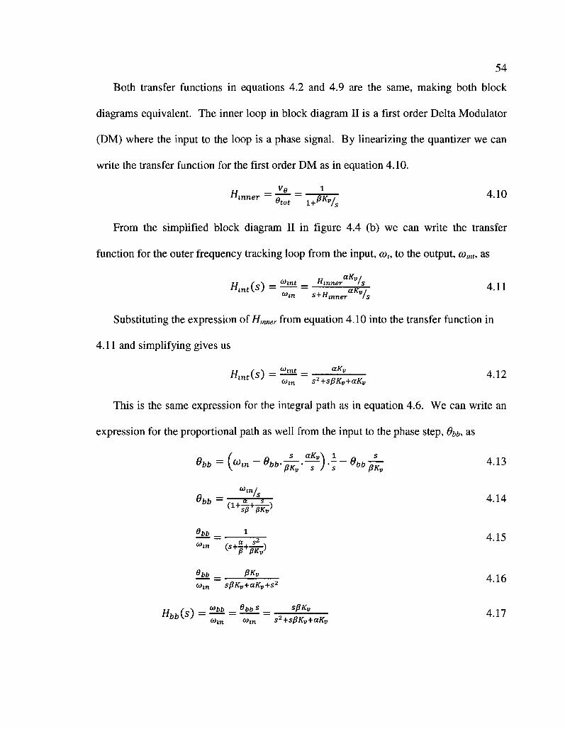
54
Both transfer functions in equations 4.2 and 4.9 are the same, making both block
diagrams equivalent. The inner loop in block diagram II is a first order Delta Modulator
(DM) where the input to the loop is a phase signal. By linearizing the quantizer we can
write the transfer function for the first order DM as in equation 4.10.
H — Ve — 1 A m
"™er-etot-i+BKv/s 4 - 1 U
From the simplified block diagram II in figure 4.4 (b) we can write the transfer
function for the outer frequency tracking loop from the input, co„ to the output, comt, as
frntfr) =^= "T^al) 4.11 Wm s+Hlnner
v/s
Substituting the expression ofHinner from equation 4.10 into the transfer function in
4.11 and simplifying gives us
Hint(s) = ^ = — ^ 4.12 lnzK J coln s2+s/3Kv+aKv
This is the same expression for the integral path as in equation 4.6. We can write an
expression for the proportional path as well from the input to the phase step, 9bb, as
^ = (^-«W£-=?)-7-«»£ 413
Jin
9bb = ^ J T 4.14 (1*sB+BKv
J
— = V 4.15
2bb = PI* 4 1 6 com spKv+aKv+s2
H f <A - ^ £ £ - 6bbS - SPKv A. 17 "bb^J-(0m a>m s2+spKv+aKv *-LI
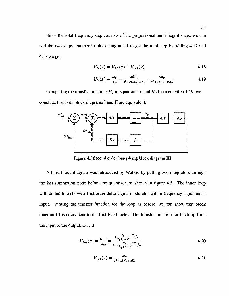
55
Since the total frequency step consists of the proportional and integral steps, we can
add the two steps together in block diagram II to get the total step by adding 4.12 and
4.17 we get:
////(s) = HM(s) + Hm£(5) 4.18
Hu(s) = ^- = SpKv cxK„
toln s2+sPKv+aKv s2+sPKv+aKv
Comparing the transfer functions Hi in equation 4.6 and HIt from equation 4.19, we
conclude that both block diagrams I and II are equivalent.
4.19
CO int
•r » i °bb.
i
1/s
Kv = ™ =
J"
A
L 1
™J
csis Kv
Figure 4.5 Second order bang-bang block diagram III
A third block diagram was introduced by Walker by pulling two integrators through
the last summation node before the quantizer, as shown in figure 4.5. The inner loop
with dotted line shows a first order delta-sigma modulator with a frequency signal as an
input. Writing the transfer function for the loop as before, we can show that block
diagram III is equivalent to the first two blocks. The transfer function for the loop from
the input to the output, comt, is
u f cA - f^iH - Vs+Wv s
HinAS) ~ ~ ys aK , 1+(VsW /s
Hm t(s) = aKv
s2+sPKv+aKv
4.20
4.21
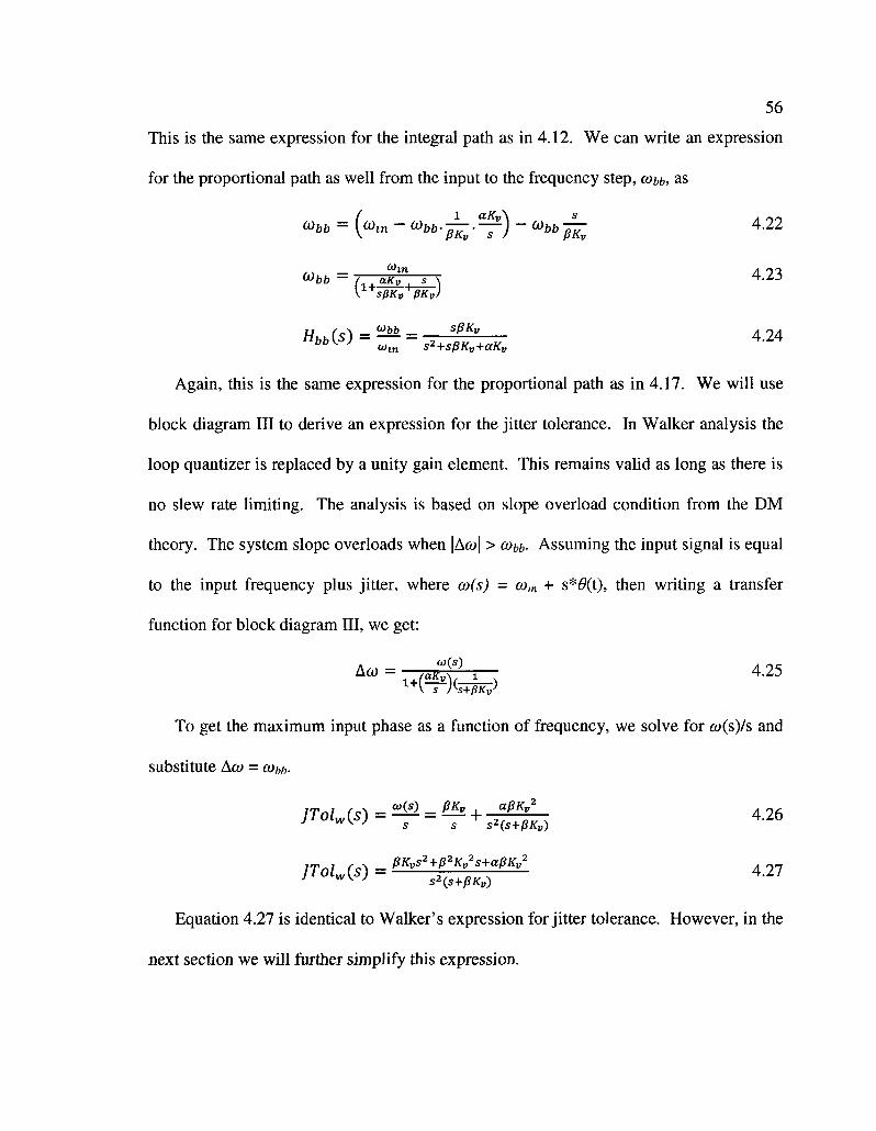
56
This is the same expression for the integral path as in 4.12. We can write an expression
for the proportional path as well from the input to the frequency step, cobb, as
( 1 <xKv\ s . __
o)in-o)bb. —.—)-o)bb— 4.22
Mbb = i aK™ s"\ 4.23 V-+sBKv
+BKv)
Hbb(s)=^ = - r ^ 4.24 w t n s2+sPKv+aKv
Again, this is the same expression for the proportional path as in 4.17. We will use
block diagram III to derive an expression for the jitter tolerance. In Walker analysis the
loop quantizer is replaced by a unity gain element. This remains valid as long as there is
no slew rate limiting. The analysis is based on slope overload condition from the DM
theory. The system slope overloads when \Aco\ > cobb- Assuming the input signal is equal
to the input frequency plus jitter, where co(s) = com + s*#(t), then writing a transfer
function for block diagram III, we get:
X1A s )^s+BKv>
To get the maximum input phase as a function of frequency, we solve for <y(s)/s and
substitute Aco = cobb-
j T o l w i s ) = ^ = B, + - ^ -
Equation 4.27 is identical to Walker's expression for jitter tolerance. However, in the
next section we will further simplify this expression.
57
4.3.2 Proposed expression for jitter tolerance
In this section a simplified expression for jitter tolerance is derived. First we analyze
equation 4.27 by partial fractions,
IT„I r<*\ PKv-a/p aKv a/p _
JTolw(s) = ^ ^ + — + ^ ^ 4.28
The third rational polynomial can be ignored since we know that:
&• » - 4.29 27T P
The left-hand side represents the (small-signal) -3dB bandwidth of the loop (for a
relatively large damping factor) while the right-hand side is equal to the closed-loop zero.
Since the loop bandwidth is typically much greater than the closed-loop zero, the above
assumption is valid [2]. We use this approximation to simplify the jitter tolerance
expression in 4.28 to yield: JTol = P5L + ?h. 4.30
s s2
A plot of the exact and simplified jitter tolerance expressions is shown in figure 4.6.
Table 3.2 was used to calculate the values for B and a and plot figure 4.6. It is clear that
our approximation is valid under the condition we mentioned in equation 4.29.
It is interesting to show that if we remove the integral path, which means a tends to
zero, the block diagram tends to a first order DM and the jitter tolerance expression
becomes:
JTollstorder = — 4.31
Equation 4.31 is the slope overload condition for a first order DM [38].
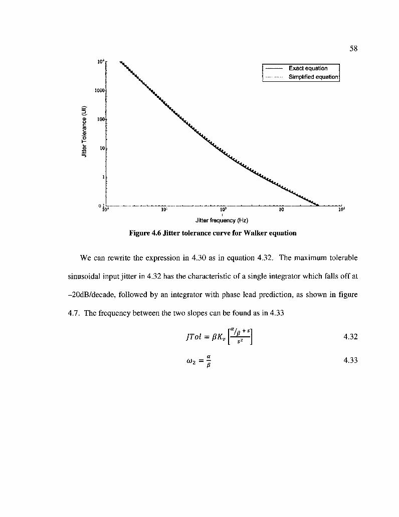
58
Exact equation Simplified equation
10* i
Jitter frequency (Hz)
10s
Figure 4.6 Jitter tolerance curve for Walker equation
We can rewrite the expression in 4.30 as in equation 4.32. The maximum tolerable
sinusoidal input jitter in 4.32 has the characteristic of a single integrator which falls off at
-20dB/decade, followed by an integrator with phase lead prediction, as shown in figure
4.7. The frequency between the two slopes can be found as in 4.33
4.32
4.33
JTol = BKV
a 2 p
\/p+S] s2
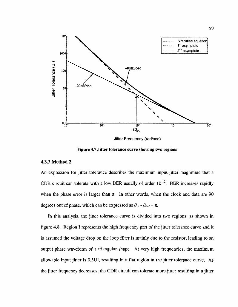
59
Jitter Frequency (rad/sec)
Figure 4.7 Jitter tolerance curve showing two regions
4.3.3 Method 2
An expression for jitter tolerance describes the maximum input jitter magnitude that a
CDR circuit can tolerate with a low BER usually of order IO"12. BER increases rapidly
when the phase error is larger than %. In other words, when the clock and data are 90
degrees out of phase, which can be expressed as 8M - 80ut = %.
In this analysis, the jitter tolerance curve is divided into two regions, as shown in
figure 4.8. Region I represents the high frequency part of the jitter tolerance curve and it
is assumed the voltage drop on the loop filter is mainly due to the resistor, leading to an
output phase waveform of a triangular shape. At very high frequencies, the maximum
allowable input jitter is 0.5UI, resulting in a flat region in the jitter tolerance curve. As
the jitter frequency decreases, the CDR circuit can tolerate more jitter resulting in a jitter
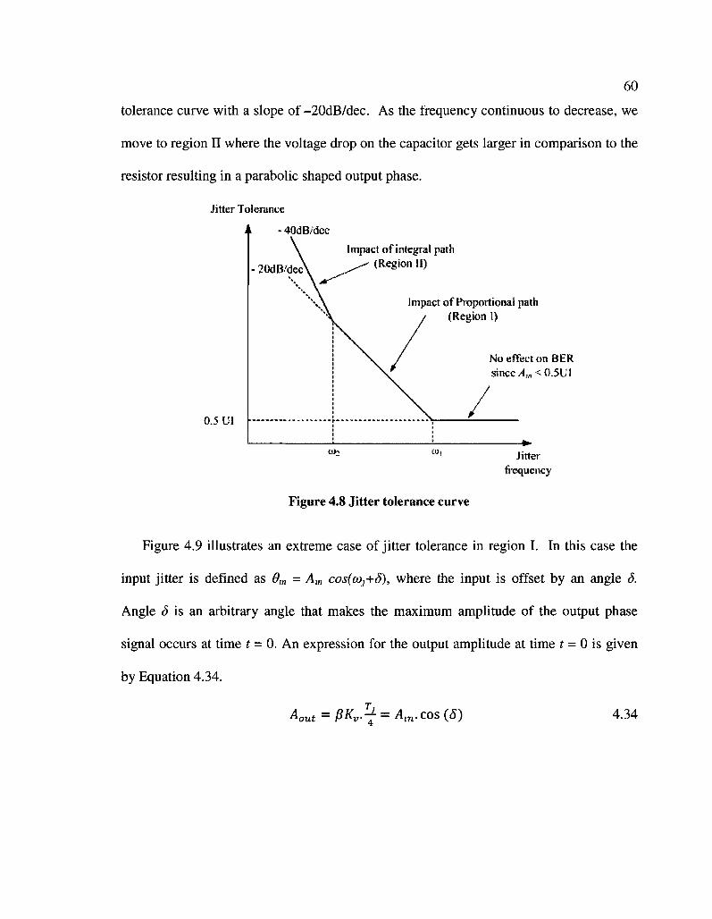
60
tolerance curve with a slope of -20dB/dec. As the frequency continuous to decrease, we
move to region II where the voltage drop on the capacitor gets larger in comparison to the
resistor resulting in a parabolic shaped output phase.
Jitter Tolerance
- 40dB/dcc
Impact of integral path < Region II)
Impact of Proportional path (Region I)
0.5 UI
No effect on BER since.4.„<0.5UI
Jitter frequency
Figure 4.8 Jitter tolerance curve
Figure 4.9 illustrates an extreme case of jitter tolerance in region I. In this case the
input jitter is defined as 9in = Ain cos(a)j+d), where the input is offset by an angle S.
Angle 3 is an arbitrary angle that makes the maximum amplitude of the output phase
signal occurs at time t = 0. An expression for the output amplitude at time t = 0 is given
by Equation 4.34.
A^ = pKv.-f = Am.cos (8) 4.34
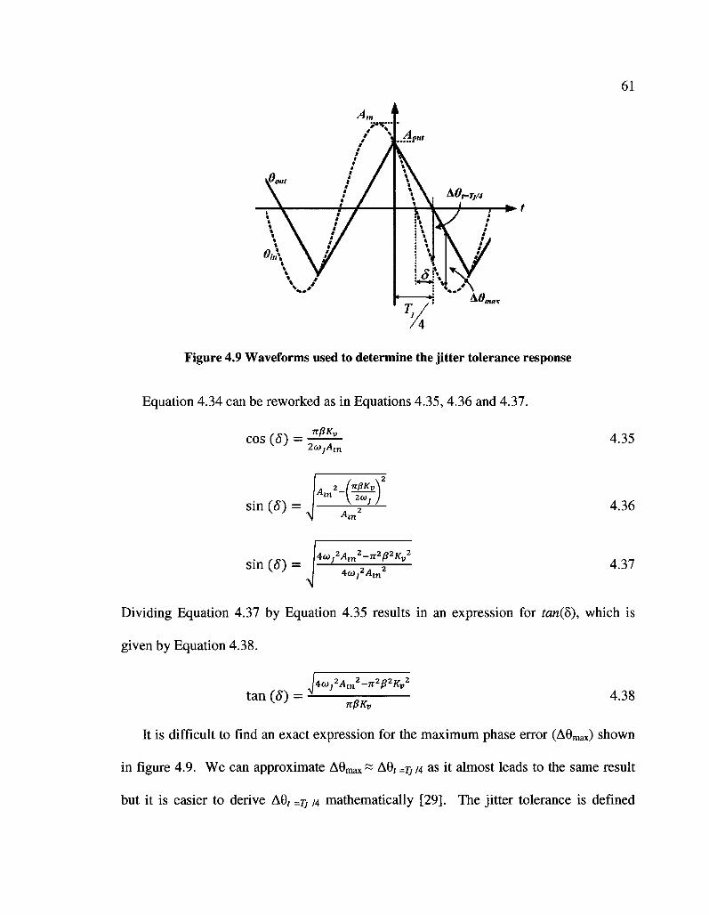
61
+~t
Figure 4.9 Waveforms used to determine the jitter tolerance response
Equation 4.34 can be reworked as in Equations 4.35,4.36 and 4.37.
npKv cos (5) =
2o)jAm
sin (5) = N
nBKv\ 2a>J )
sin (8) = \4to}
2Aln2-n2p2Kv
2
4tOj2Aln2
4.35
4.36
4.37
Dividing Equation 4.37 by Equation 4.35 results in an expression for tan(5), which is
given by Equation 4.38.
Ua>2Aln2-n2p2Kv
2
° » « J 55 4.38
It is difficult to find an exact expression for the maximum phase error (A9max) shown
in figure 4.9. We can approximate A0max ~ A9f =T, IS, as it almost leads to the same result
but it is easier to derive AG, =TJ IA mathematically [29]. The jitter tolerance is defined
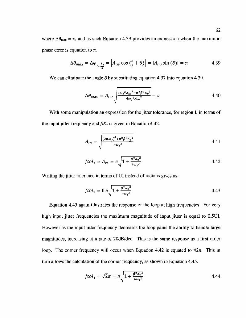
62
where A0max = n, and as such Equation 4.39 provides an expression when the maximum
phase error is equation to 7t.
&9max « Acp Tj= Ain. cos (J + 5) = \Am.sin {8)\=n 4.39 4
We can eliminate the angle 3 by substituting equation 4.37 into equation 4.39.
With some manipulation an expression for the jitter tolerance, for region I, in terms of
the input jitter frequency and BKV is given in Equation 4.42.
ln I 4to}2
Jtol1=Ain = nJl+^4 4.42 4a>j
Writing the jitter tolerance in terms of UI instead of radians gives us,
Jtoll = 0.5 J i + ^ 4.43
Equation 4.43 again illustrates the response of the loop at high frequencies. For very
high input jitter frequencies the maximum magnitude of input jitter is equal to 0.5UI.
However as the input jitter frequency decreases the loop gains the ability to handle large
magnitudes, increasing at a rate of 20dB/dec. This is the same response as a first order
loop. The corner frequency will occur when Equation 4.42 is equated to V2TI. This in
turn allows the calculation of the corner frequency, as shown in Equation 4.45.
P2Kv Jtok = V2TT = ir 1 + £ J ^ - 4.44
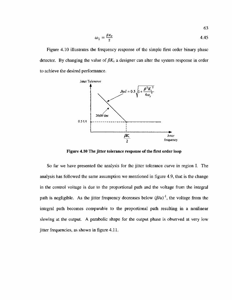
Wi = PKv
63
4.45
Figure 4.10 illustrates the frequency response of the simple first order binary phase
detector. By changing the value of BKV a designer can alter the system response in order
to achieve the desired performance.
Jitter Tolerance A
0.5 UI
./to* =0.5 1 + /?X2
4®,
2
Jitter frequency
Figure 4.10 The jitter tolerance response of the first order loop
So far we have presented the analysis for the jitter tolerance curve in region I. The
analysis has followed the same assumption we mentioned in figure 4.9, that is the change
in the control voltage is due to the proportional path and the voltage from the integral
path is negligible. As the jitter frequency decreases below (fi/a)~x, the voltage from the
integral path becomes comparable to the proportional path resulting in a nonlinear
slewing at the output. A parabolic shape for the output phase is observed at very low
jitter frequencies, as shown in figure 4.11.
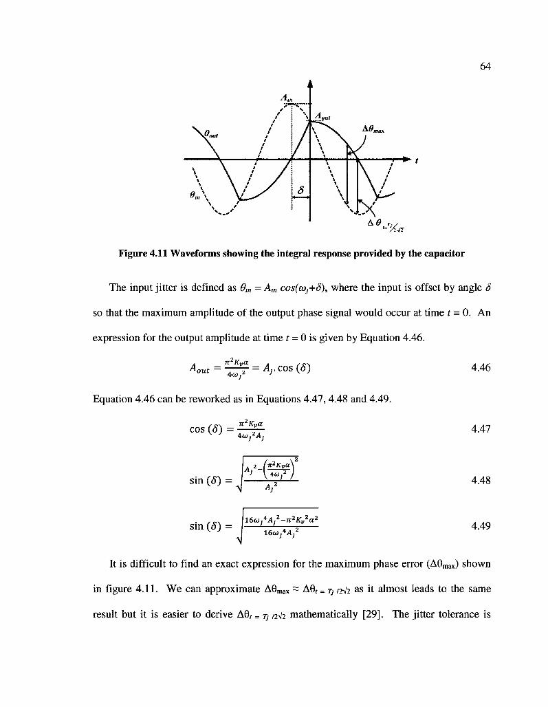
64
r-+*r
A e Tj/
Figure 4.11 Waveforms showing the integral response provided by the capacitor
The input jitter is defined as 9m = Ain cos(coj+3), where the input is offset by angle 8
so that the maximum amplitude of the output phase signal would occur at time / = 0. An
expression for the output amplitude at time t = 0 is given by Equation 4.46.
**mit — lOUt n2Kva
4coj2 = Aj. cos (8)
Equation 4.46 can be reworked as in Equations 4.47, 4.48 and 4.49.
n2Kva cos (5) =
4ojj2Aj
sin(5)= llA^ll
. , „ , \l6o)*A2-n2Kv2a2
sin (8) = — ' ' , ,
4.46
4.47
4.48
4.49
It is difficult to find an exact expression for the maximum phase error (A0max) shown
in figure 4.11. We can approximate A0max ~ AG, = T} /2V2 as it almost leads to the same
result but it is easier to derive AG, = TJ /2V2 mathematically [29]. The jitter tolerance is
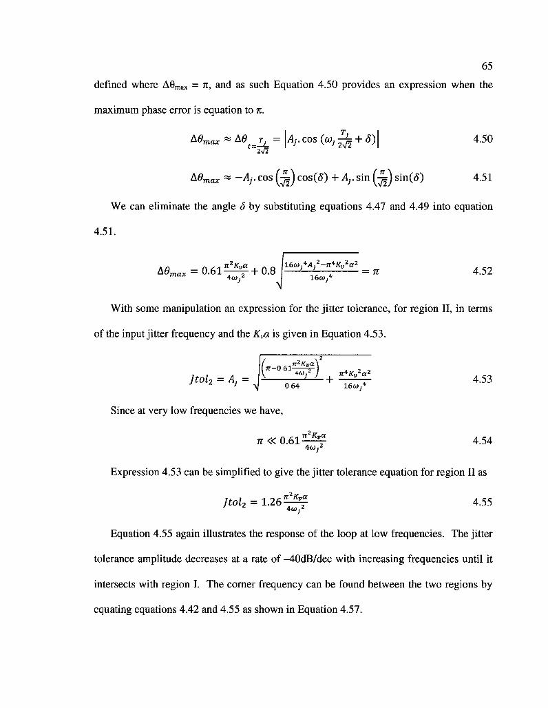
65
defined where A9max = n, and as such Equation 4.50 provides an expression when the
maximum phase error is equation to n.
k9max « A9 _Tj_ = A/.cos (co,-^j= + S) 4.50 "2V2
Aj.cos(o)j^= + S)
h9max « -Aj. cos (^=) cos(5) + Aj. sin (^=) sin(5) 4.51
We can eliminate the angle 3 by substituting equations 4.47 and 4.49 into equation
4.51.
Mmax = o.6ito* + 0.8 ^ / V - ^ v « » = n 452 max 4cOj2 16co ;
4
With some manipulation an expression for the jitter tolerance, for region II, in terms
of the input jitter frequency and the Kva is given in Equation 4.53.
A |(-"'gf)', ^ } ^ 0 64 16cOj* jtol2 =A,= P ^ + ^ ^ 4.53
Since at very low frequencies we have,
n2Kva 7 r « 0 . 6 1 ^ P 4.54 4co,2
Expression 4.53 can be simplified to give the jitter tolerance equation for region II as
Jtol2 = 1.26 ^ f 4.55 J L 4wj2
Equation 4.55 again illustrates the response of the loop at low frequencies. The jitter
tolerance amplitude decreases at a rate of -40dB/dec with increasing frequencies until it
intersects with region I. The comer frequency can be found between the two regions by
equating equations 4.42 and 4.55 as shown in Equation 4.57.
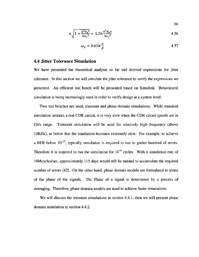
66
w / ! + £ £ ! = 1.26=^? 4.56 -\| 4o j j z 4t0j2
co2 = 0.63rr^ 4.57
4.4 Jitter Tolerance Simulation
We have presented the theoretical analysis so far and derived expressions for jitter
tolerance. In this section we will simulate the jitter tolerance to verify the expressions we
presented. An efficient test bench will be presented based on Simulink. Behavioural
simulation is being increasingly used in order to verify design at a system level.
Two test benches are used, transient and phase-domain simulations. While transient
simulation imitates a real CDR circuit, it is very slow when the CDR circuit speeds are in
Gb/s range. Transient simulation will be used for relatively high frequency (above
lOKHz), as below that the simulation becomes extremely slow. For example, to achieve
a BER below IO"12, typically simulation is required to run to gather hundred of errors.
Therefore it is required to mn the simulation for IO14 cycles. With a simulation rate of
lOMcycles/sec, approximately 115 days would still be needed to accumulate the required
number of errors [42]. On the other hand, phase domain models are formulated in terms
of the phase of the signals. The Phase of a signal is determined by a process of
averaging. Therefore, phase domain models are used to achieve faster simulations.
We will discuss the transient simulations in section 4.4.1, then we will present phase
domain simulation in section 4.4.2.
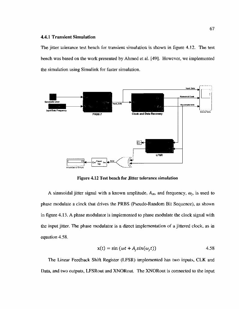
67
4.4.1 Transient Simulation
The jitter tolerance test bench for transient simulation is shown in figure 4.12. The test
bench was based on the work presented by Ahmed et al. [49]. However, we implemented
the simulation using Simulink for faster simulation.
Sinusoidal Jitter
Input Data Frequency
PRBS7 Clock and Data Recovery
0 j «
(vSnumber of Errors
Figure 4.12 Test bench for Jitter tolerance simulation
A sinusoidal jitter signal with a known amplitude, A,n, and frequency, cop is used to
phase modulate a clock that drives the PRBS (Pseudo-Random Bit Sequence), as shown
in figure 4.13. A phase modulator is implemented to phase modulate the clock signal with
the input jitter. The phase modulator is a direct implementation of a jittered clock, as in
equation 4.58.
x(t) = sin (o>t + AjSin(a)jt)) 4.58
The Linear Feedback Shift Register (LFSR) implemented has two inputs, CLK and
Data, and two outputs, LFSRout and XNORout. The XNORout is connected to the input
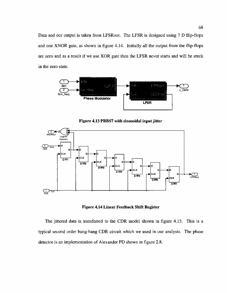
68
Data and our output is taken from LFSRout. The LFSR is designed using 7 D flip-flops
and one XNOR gate, as shown in figure 4.14. Initially all the output from the flip-flops
are zero and as a result if we use XOR gate then the LFSR never starts and will be stuck
in the zero state.
Dm_freq
J_Data
Figure 4.13 PRBS7 with sinusoidal input jitter
XNORout ^ ^ A X Logical
Operator
CChsr-Data
V ) CLK CLK
CLK
DFF1 CLK
DFP2
DFR3 CLK
DFF4 CLK
DFF5
DFFB
DFF7
-KID
Figure 4.14 Linear Feedback Shift Register
The jittered data is transferred to the CDR model shown in figure 4.15. This is a
typical second order bang-bang CDR circuit which we used in our analysis. The phase
detector is an implementation of Alexander PD shown in figure 2.8.
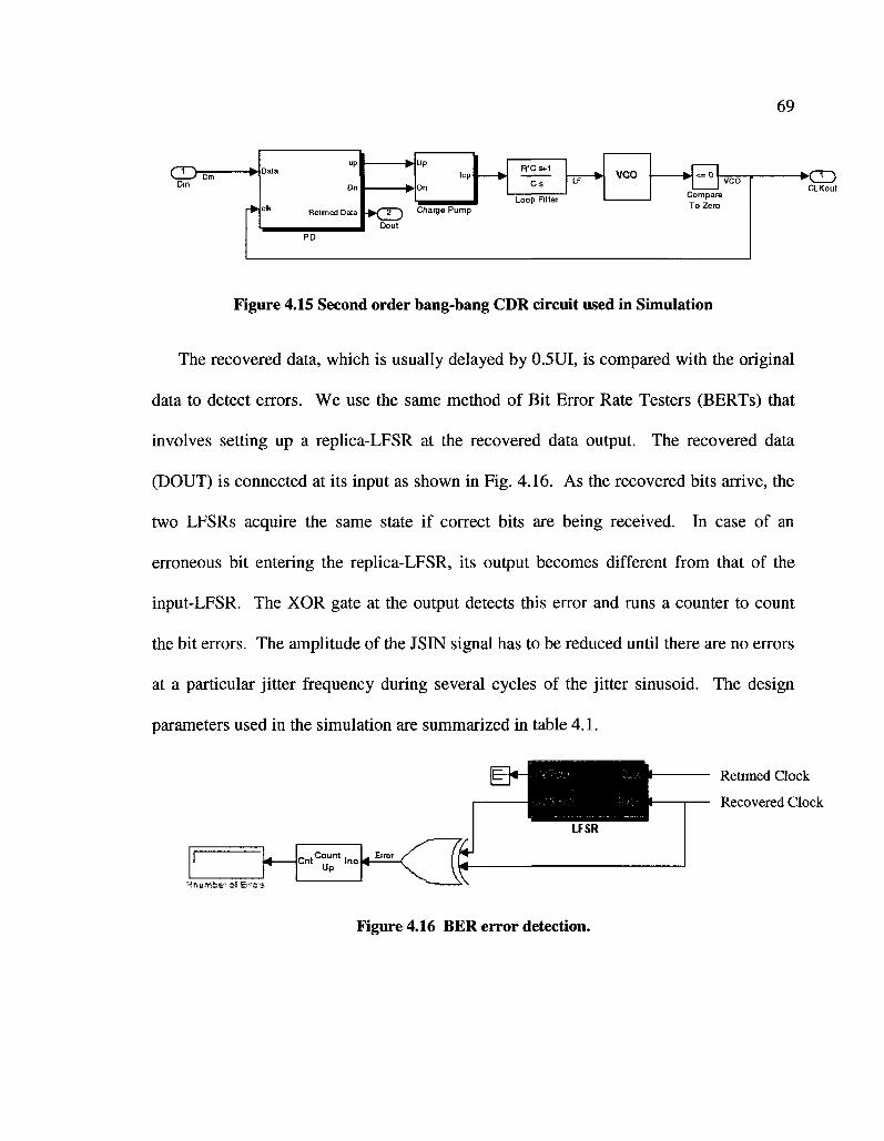
69
Din
Data
elk
up
Dn
Retimed Data
p.
Dout
Up
Icp
Dn
Charge Pump
R*Csf1
Cs LF VCO < = 0
To Zero
-KID CLKout
Figure 4.15 Second order bang-bang CDR circuit used in Simulation
The recovered data, which is usually delayed by 0.5UI, is compared with the original
data to detect errors. We use the same method of Bit Error Rate Testers (BERTs) that
involves setting up a replica-LFSR at the recovered data output. The recovered data
(DOUT) is connected at its input as shown in Fig. 4.16. As the recovered bits arrive, the
two LFSRs acquire the same state if correct bits are being received. In case of an
erroneous bit entering the replica-LFSR, its output becomes different from that of the
input-LFSR. The XOR gate at the output detects this error and runs a counter to count
the bit errors. The amplitude of the JSIN signal has to be reduced until there are no errors
at a particular jitter frequency during several cycles of the jitter sinusoid. The design
parameters used in the simulation are summarized in table 4.1.
ReUmed Clock
Recovered Clock
Mnumbs^ of Ef^o^s
Figure 4.16 BER error detection.
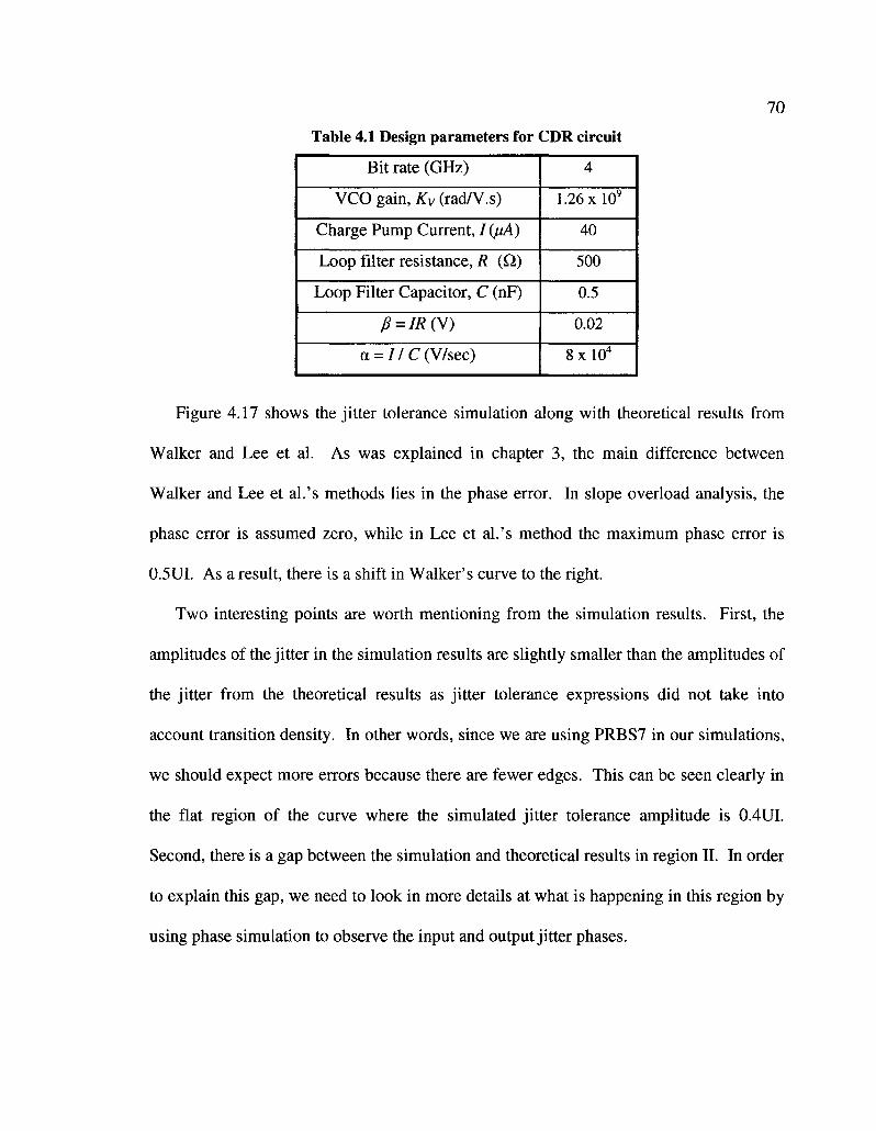
70
Table 4.1 Design parameters for CDR circuit
Bit rate (GHz)
VCO gain, £,/(rad/V.s)
Charge Pump Current, I(juA)
Loop filter resistance, R (Q)
Loop Filter Capacitor, C (nF)
P = IRCf)
a = //C(V/sec)
4
1.26 x IO9
40
500
0.5
0.02
8xl0 4
Figure 4.17 shows the jitter tolerance simulation along with theoretical results from
Walker and Lee et al. As was explained in chapter 3, the main difference between
Walker and Lee et al.'s methods lies in the phase error. In slope overload analysis, the
phase error is assumed zero, while in Lee et al.'s method the maximum phase error is
0.5UI. As a result, there is a shift in Walker's curve to the right.
Two interesting points are worth mentioning from the simulation results. First, the
amplitudes of the jitter in the simulation results are slightly smaller than the amplitudes of
the jitter from the theoretical results as jitter tolerance expressions did not take into
account transition density. In other words, since we are using PRBS7 in our simulations,
we should expect more errors because there are fewer edges. This can be seen clearly in
the flat region of the curve where the simulated jitter tolerance amplitude is 0.4UI.
Second, there is a gap between the simulation and theoretical results in region II. In order
to explain this gap, we need to look in more details at what is happening in this region by
using phase simulation to observe the input and output jitter phases.
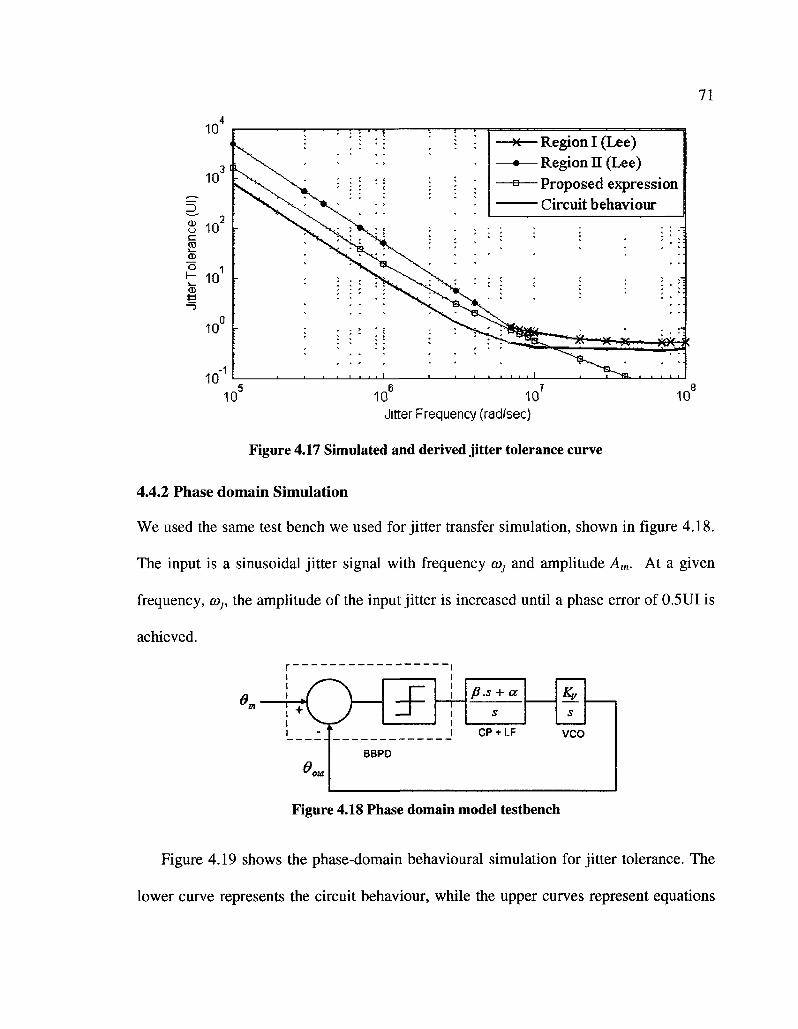
71
o
10 10 Jitter Frequency (rad/sec)
Figure 4.17 Simulated and derived jitter tolerance curve
4.4.2 Phase domain Simulation
We used the same test bench we used for jitter transfer simulation, shown in figure 4.18.
The input is a sinusoidal jitter signal with frequency co, and amplitude Am. At a given
frequency, cop the amplitude of the input jitter is increased until a phase error of 0.5UI is
achieved.
0
r
! { +v i Qom
y^ i
:F BBPD
P .s + a s
CP + LF
|
s
VCO
Figure 4.18 Phase domain model testbench
Figure 4.19 shows the phase-domain behavioural simulation for jitter tolerance. The
lower curve represents the circuit behaviour, while the upper curves represent equations
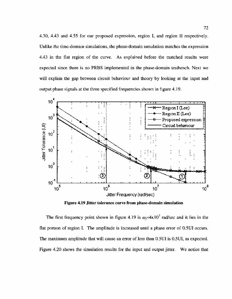
72
4.30, 4.43 and 4.55 for our proposed expression, region I, and region II respectively.
Unlike the time-domain simulations, the phase-domain simulation matches the expression
4.43 in the flat region of the curve. As explained before the matched results were
expected since there is no PRBS implemented in the phase-domain testbench. Next we
will explain the gap between circuit behaviour and theory by looking at the input and
output phase signals at the three specified frequencies shown in figure 4.19.
5 6 7 8
10 10 10 10
Jitter Frequency (rad/sec)
Figure 4.19 Jitter tolerance curve from phase-domain simulation
The first frequency point shown in figure 4.19 is C0j=4x\07 rad/sec and it lies in the
flat portion of region I. The amplitude is increased until a phase error of 0.5UI occurs.
The maximum amplitude that will cause an error of less than 0.5UI is 0.5UI, as expected.
Figure 4.20 shows the simulation results for the input and output jitter. We notice that
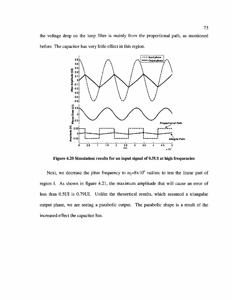
73
the voltage drop on the loop filter is mainly from the proportional path, as mentioned
before. The capacitor has very little effect in this region.
Proportional Path
\ Integral Path
Figure 4.20 Simulation results for an input signal of 0.5UI at high frequencies
Next, we decrease the jitter frequency to w7=8xl06 rad/sec to test the linear part of
region I. As shown in figure 4.21, the maximum amplitude that will cause an error of
less than 0.5UI is 0.79UI. Unlike the theoretical results, which assumed a triangular
output phase, we are seeing a parabolic output. The parabolic shape is a result of the
increased effect the capacitor has.
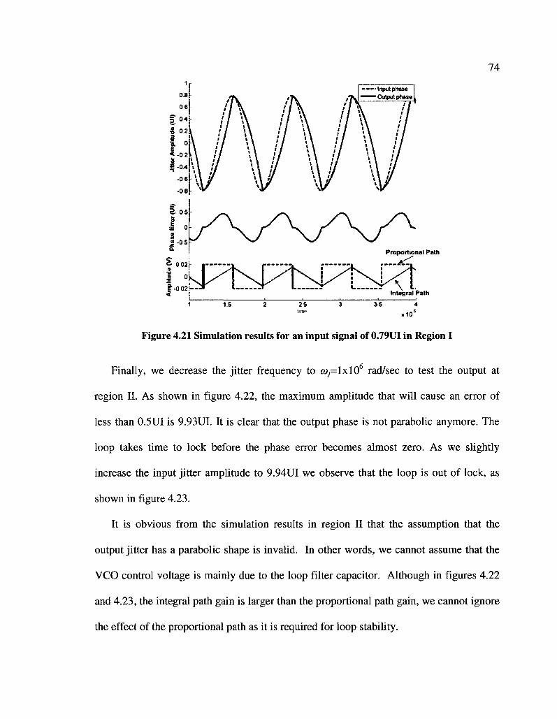
74
-—Inpu t phase - Output phase
2 0 02
I
Proportional Path
I j i J ^ f c J ^ f c d ^ ^ Integral Path
1.5 25 35 x10"
Figure 4.21 Simulation results for an input signal of 0.79UI in Region I
Finally, we decrease the jitter frequency to <y,=lxl06 rad/sec to test the output at
region II. As shown in figure 4.22, the maximum amplitude that will cause an error of
less than 0.5UI is 9.93UI. It is clear that the output phase is not parabolic anymore. The
loop takes time to lock before the phase error becomes almost zero. As we slightly
increase the input jitter amplitude to 9.94UI we observe that the loop is out of lock, as
shown in figure 4.23.
It is obvious from the simulation results in region II that the assumption that the
output jitter has a parabolic shape is invalid. In other words, we cannot assume that the
VCO control voltage is mainly due to the loop filter capacitor. Although in figures 4.22
and 4.23, the integral path gain is larger than the proportional path gain, we cannot ignore
the effect of the proportional path as it is required for loop stability.
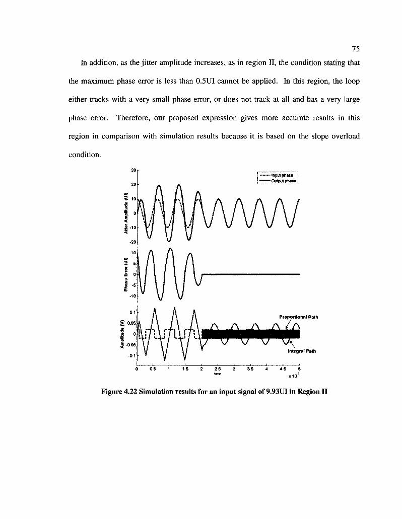
75
In addition, as the jitter amplitude increases, as in region II, the condition stating that
the maximum phase error is less than 0.5UI cannot be applied. In this region, the loop
either tracks with a very small phase error, or does not track at all and has a very large
phase error. Therefore, our proposed expression gives more accurate results in this
region in comparison with simulation results because it is based on the slope overload
condition.
Proportional Path
L \ Integral Path
x10
Figure 4.22 Simulation results for an input signal of 9.93UI in Region II
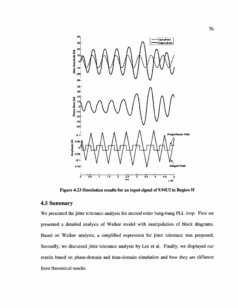
76
Proportional Path
Integral Path
05 15 25 ttme
3.5 4 5 5
«105
Figure 4.23 Simulation results for an input signal of 9.94UI in Region II
4.5 Summary
We presented the jitter tolerance analysis for second order bang-bang PLL loop. First we
presented a detailed analysis of Walker model with manipulation of block diagrams.
Based on Walker analysis, a simplified expression for jitter tolerance was proposed.
Secondly, we discussed jitter tolerance analysis by Lee et al. Finally, we displayed our
results based on phase-domain and time-domain simulation and how they are different
from theoretical results.
77
Chapter 5: Conclusion
5.1 Conclusion
A detailed analysis of jitter transfer and jitter tolerance characteristics of second order
bang-bang PLL loop was presented throughout the thesis. Literature review has shown
that bang-bang phase detectors are widely used in CDR circuits for high speed serial
communications for its superior performance.
A selected number of previous papers modeling and analyzing bang-bang PLL loops
for jitter performance were presented. While there has been a number of methods
developed to model the loop, no attempt has been made to unify different methods and
investigate the variations of the proposed analysis. In chapter two we briefly presented
most of the methods used and our analysis was restricted to two main methods, namely
Walker's and Lee et al.'s.
Chapter three revolves around the discussion of Walker and Lee et al.'s methods for
jitter transfer analysis. Throughout the chapter, the definition of jitter transfer was given
according to the standards resulting in a modified expression that complies with the
definition. In addition, a phase domain testbench was developed for jitter transfer
simulation using Simulink and the simulation results showed favorable agreement with
our derived expression.
78
In chapter 4 we investigated the jitter tolerance analysis presented by Walker and Lee
et al. Different block diagrams developed by Walker were accurately analyzed and
verified by means of transfer functions. This analysis gave us a better understanding of
the dynamics of the loop. Next we presented the jitter tolerance expression derived by
Walker and using mathematical tools this expression was simplified further. Walker'
analysis was based on Delta Modulator conventional theory while Lee et al.'s method
was based on large-signal piecewise-linear model. Lee et al. divided the jitter tolerance
curve into two regions depending on the effect of the loop filter capacitor. Jitter tolerance
expressions for each region were rederived and verified.
Finally, novel analysis for jitter tolerance was verified using time-domain and phase-
domain simulations. Based on simulation results we were able to explain the loop
behaviour in each region of the jitter tolerance curve. Although, simulation results
showed good agreement with Lee et al.'s theoretical results in region I, in region II the
simulation results did not match the theoretical work. On the other hand, a simplified
expression based on Walker's method showed close agreement with simulation results in
region II.
5.2 Contributions
The understanding of bang-bang PLL loop and related jitter transfer and jitter tolerance
characteristics have been enhanced through the following contributions:
• A detailed jitter transfer analysis for Walker and Lee et al.'s work in
considerable depth. An expression was proposed that complies with the
79
definition of jitter transfer. A paper was successfully published in an IEEE
conference on this work [45],
• An indepth investigation of the manipulation of Walker's block diagram for
second order bang-bang PLL loop. Transfer functions of the block diagrams
were used as a tool to show the equivalence of the developed block diagrams,
• The development of a simplified expression for jitter tolerance based on
Walker's work, as in equation 4.30,
• A novel analysis explaining the behaviour of the loop in each region of the
jitter tolerance curve by means of behavioural simulations. Simulation results
showed the shortcomings of Lee et al.'s expression in region II due to invalid
assumptions.
5.3 Future Work
There are several ways in which the research presented in this thesis can be further
pursued:
• In our analysis we assumed only deterministic jitter; random jitter can be
included in the analysis as a practical case,
• The effect of metastability and jitter on bang-bang phase detector response
can be further examined,
• The analysis can be extended to include jitter generation and BER as well.
Jitter generation and BER are not fully investigated in the literature yet.
[1] R. Walker, "Designing Bang-bang PLLs for Clock and Data Recovery in Serial Data Transmission Systems," Phase-Locking in High-Performance Systems -from devices to Architectures, B. Razavi, IEEE press, 2003, pp. 34-45.
[2] B. Razavi, Design of integrated circuits for optical communications, New York: McGraw-Hill, 2003.
[3] J. Savoj and B. Razavi, High-speed CMOS circuits for optical receivers, Netherlands: Springer, 2001.
[4] R. Walker, C. Stout, J. Wu, B. Lai, C. Yen, T. Hornak, and P. Petruno, "A Two-Chip 1. 5-GBd Serial Link Interface," Journal of Solid-State Circuits, vol. 27, 1992, pp.1805-1811.
[5] A. Pottbacker, U. Langmann, and H. Schreiber, "A Si Bipolar Phase and Frequency Detector IC for Clock Extraction up to 8 Gb/s," Journal of Solid-State Circuits, vol. 27,1992, pp. 1747-1751.
[6] J.L. Sonntag and J. Stonick, "A Digital Clock and Data Recovery Architecture for Multi-Gigabit/s Binary Links," Journal of Solid-State Circuits, vol. 41, Aug. 2006, pp. 1867-1875.
[7] H. Chang, R. Yang, and S. Liu, "Low Jitter and Multirate Clock and Data Recovery Circuit Using a MSADLL for Chip-to-Chip Interconnection," IEEE Transactions on Circuits and Systems I, vol. 51, Dec. 2004, pp. 2356-2364.
[8] K.H. Cheng, P.K. Tseng, and Y.L. Lo, "A Phase Interpolator For Sub-IV And High Frequency For Clock And Data Recovery," Electronics, Circuits and Systems, 2007. ICECS 2007. 14th IEEE International Conference on, IEEE, 2008, p. 363-366.
[9] J. Lee and M. Liu, "A 20-Gb/s Burst-Mode Clock and Data Recovery Circuit Using Injection-Locking Technique," Journal of Solid-State Circuits, vol. 43, Mar. 2008, pp. 619-630.
81
[10] J.H.C. Zhan, J.S. Duster, and K.T. Kornegay, "A Full-rate injection-locked 10.3 Gb/s clock and data recovery circuit in a 45GHz-f T SiGe process," Proceedings of the Custom Integrated Circuits Conference, 2005, p. 557-560.
[11] S. Ahmed and T. Kwasniewski, "Overview of Oversampling Clock and Data Recovery Circuits," Canadian Conference on Electrical and Computer Engineering, 2005, pp. 1876-1881.
[12] M. Hsieh and G. Sobelman, "Architectures for multi-gigabit wire-linked clock and data recovery," IEEE Circuits and Systems Magazine, vol. 8, 2008, pp. 45-57.
[13] D. Rennie and M. Sachdev, "Comparative Robustness of CML Phase Detectors for Clock and Data Recovery Circuits," Proceedings of the 8th International Symposium on Quality Electronic Design, 2007, pp. 305-310.
[14] C. Hogge, "A Self Correcting Clock Recovery Circuit," Journal of Lightwave Technology, vol. 3, 1985, pp. 1312-1314.
[15] D. Shin, M. Park, and M. Lee, "Self-correcting clock recovery circuit with improved jitter performance," Electronics Letters, 1987, pp. 110-111.
[16] L. DeVito, "Phase detector for phase-locked loop clock recovery system," US Patent 5 027 085 , Jun. 25,1991.
[17] L. DeVito, "A versatile clock recovery architecture and monolithic implementation," MONOLITHIC PHASE-LOCKED LOOPS AND CLOCK RECOVERY CIRCUITS, B. Razavi, ed., Wiley, 1996, pp. 405-420.
[18] Y. Greshishchev and P. Schvan, "SiGe clock and data recovery IC with linear-type PLL for 10-Gb/s SONET application," IEEE Journal of Solid-State Circuits, vol. 35, 2000, pp.1353-1359.
[19] Y. Ohtomo, K. Nishimura, and M. Nogawa, "A 12.5-Gb/s Parallel Phase Detection Clock and Data Recovery Circuit in 0.13-u.m CMOS," IEEE Journal of Solid-State Circuits, vol. 41, Sep. 2006, pp. 2052-2057.
[20] D. Rennie and M. Sachdev, "A 5-Gb/s CDR circuit with automatically calibrated linear phase detector," IEEE Transactions on Circuits and Systems I, 2008, pp. 796-803.
[21] B. Razavi, "Challenges in the design of high-speed clock and data recovery circuits," IEEE Communications Magazine, 2002, pp. 94-101.

[22] J. Alexander, "Clock recovery from random binary data," Electronics letters, vol. 11, 1975, pp. 541-542.
[23] "Jitter in Digital Communication Systems , Part 1," http://www.maxim-ic.com/app-notes/index.mvp/id/794, 2001, pp. 1-7.
[24] A. Kuo, T. Farahmand, N. Ou, S. Tabatabaei, and A. Ivanov, "Jitter models and measurement methods for high-speed serial interconnects," Proceedings on International Test Conference, 2004, pp. 1295-1302.
[25] "Converting between RMS and Peak-to-Peak Jitter at a Specified BER," http://www.maxim-ic.com/app-notes/index.mvp/id/462, 2000, pp. 1-5.
[26] "Jitter Analysis Techniques for High Data Rates," http://cp. literature, agilent. com/litweb/pdfZ5988-8425EN.pdf, 2003.
[27] A. Alpert, "Jitter Measurements in Telecom Transmission Systems," http://www.jdsu. com/ProductLiterature/jitter-accuracy_wp_opt_tm_ae.pdf, 2008.
[28] Telecordi Technologies, Synchronous Optical Network (SONET) Transport Systems: Common Generic Criteria, 2000.
[29] J. Lee, K. Kundert, and B. Razavi, "Analysis and modeling of bang-bang clock and data recovery circuits," IEEE Journal of Solid-State Circuits, vol. 39, 2004, pp. 1571-1580.
[30] N.D. Dalt, "Linearized Analysis of a Digital Bang-Bang PLL and Its Validity Limits Applied to Jitter Transfer and Jitter Generation," IEEE Transactions on Circuits and Systems, vol. 55, 2008, pp. 3663-3675.
[31] N.D. Dalt, "A Design-Oriented Study of the Nonlinear Dynamics of Digital Bang-Bang PLLs," IEEE Transactions on Circuits and Systems, vol. 52, 2005, pp. 21-31.
[32] S. Cheng, H. Tong, J. Silva-Martinez, and A. Karsilayan, "Steady-State Analysis of Phase-Locked Loops Using Binary Phase Detector," IEEE Transactions on Circuits and Systems, vol. 54, 2007, pp. 474-478.
[33] S. Tertinek, J.P. Gleeson, and O. Feely, "Statistical Analysis of First-Order Bang-Bang Phase-Locked Loops Using Sign-Dependent Random Walk Theory," IEEE Transactions on Circuits and Systems, vol. 57, 2010, pp. 2367-2380.
83
[34] Y. Sun and H. Wang, "Analysis of Digital Bang-Bang Clock and Data Recovery for Multi-Gigabit/s Serial Transceivers," Custom Integrated Circuits Conference, 2009, pp. 343-346.
[35] Y. Greshishchev, P. Schvan, and J. Showell, "A fully integrated SiGe receiver IC for 10-Gb/s data rate," IEEE Journal of Solid-State Circuits, vol. 35, 2000, pp. 1949 -1957.
[36] M. Ramezani, C. Andre, and T. Salama, "Jitter analysis of a PLL-based CDR with a bang-bang phase detector," The 45th Midwest Symposium on Circuits and Systems, 2002, p. III-393-III-396.
[37] M. Ramezani, C. Andre, and T. Salama, "Analysis of a Half-Rate Bang-Bang Phase-Locked-Loop," IEEE Transactions on Circuits and Systems, vol. 49, 2002, pp. 505-509.
[38] R. Steele, Delta Modulation Systems, Pentech Press & Halsted Press, 1975.
[39] S. Wang, H. Mei, M. Baig, W. Bereza, and T. Kwasniewski, R, "Design Considerations for 2nd-Order and 3rd-Order Bang-Bang CDR Loops," Custom Integrated Circuits Conference, 2005, pp. 317-320.
[40] M. Chan, A. Postula, Y. Ding, and L. Jozwiak, "A bang-bang PLL employing dynamic gain control for low jitter and fast lock times," Analog Integrated Circuits And Signal Processing, vol. 49, 2006, pp. 131-140.
[41] M. Chan and A. Postula, "Transient analysis of bang-bang phase locked loops," IET Circuits, Devices & Systems, vol. 3, 2009, pp. 76-82.
[42] K. Kundert, "Verification of Bit-Error Rate in Bang-Bang Clock and Data Recovery Circuits," The Designer's Guide Community, 2010, pp. 1-22.
[43] D. Hong and K. Cheng, "Bit-Error Rate Estimation for Bang-Bang Clock and Data Recovery Circuit in High-Speed Serial Links," 26th IEEE VLSI Test Symposium, 2008, pp. 17-22.
[44] Y. Choi, D. Jeong, and W. Kim, "Jitter transfer analysis of tracked oversampling techniques for multigigabit clock and data recovery," IEEE Transactions on Circuits and Systems, vol. 50, 2003, pp. 775-783.
[45] A. Gabr and T. Kwasniewski, "Unifying approach for jitter transfer analysis of bang-bang CDR circuits," International Conference on Electronics and Information Engineering, 2010, pp. 40-44.
[46] R. Neil, "Understanding Jitter and Wander Measurements and Standards, http://cp.literature.agilent.com/litweb/pdf/5988-6254EN.pdf, 2003, p. ch 11.
[47] A. Gelb and W.E. Vander Velde, Multiple-input describing functions and nonlinear system design, McGraw-Hill, 1968.
[48] F. Musa and A. Carusone, "Modeling and Design of Multilevel Bang-Bang CDRs in the Presence of ISI and Noise," IEEE Transactions Circuits and Systems, vol. 54, 2007, pp. 2137-2147.
[49] S.I. Ahmed, K. Orthner, and T. Kwasniewski, "Behavioral Test Benches for Digital Clock and Data Recovery Circuits using Verilog-A," Custom Integrated Circuits Conference, 2005, pp. 290-293.