introduction to nanotechnology
DESCRIPTION
Introduction to Nanotechnology. Mark Tuominen Professor of Physics UMass Amherst. Nanotechnology. What, How, Why?. Nanotechnology. The biggest science initiative since the Apollo program. Nanotechnology. - PowerPoint PPT PresentationTRANSCRIPT

Introduction to NanotechnologyIntroduction to Nanotechnology
Mark TuominenProfessor of Physics
UMass Amherst
Nanotechnology
What, How, Why?

NanotechnologyThe biggest science initiative
since the Apollo program

Nanotechnology
Nanotechnology is the understanding and control of matter at dimensions of roughly 1 to 100 nanometers, where unique phenomena enable novel applications.
1 nanometer = 1 billionth of a meter= 1 x 10⁻⁹ m
nano.gov

How small are nanostructures?
Single Hair
Width = 0.1 mm
= 100 micrometers
= 100,000 nanometers !

Smaller still
Hair
. QuickTime™ and aTIFF (LZW) decompressor
are needed to see this picture.
6,000 nanometersDNA
3 nanometers
100,000 nanometers
10 nm objectsmade by guided
self-assembly

Nanotechnology
Is it a truly a new field?Is it all hype?

10 GB2001
20 GB2002
40 GB2004
80 GB2006
160 GB2007
Example: Data storage capacity of the iPod
Hard driveMagnetic data storage
Uses nanotechnology!

Hard Disk Drives - a home for bits
Hitachi

Magnetic Data StorageA computer hard drive stores your data magnetically
Disk
N S
direction of disk motion
“ Write”Head
0 0 1 0 1 0 0 1 1 0 _ _
“ Bits” ofinformation
NS
“ Read”Head
Signalcurrent

Improving Magnetic Data Storage Technology
• The UMass Amherst Center for Hierarchical Manufacturing is working to improve this technology
Granular Media
PerpendicularWrite Head
Soft Magnetic UnderLayer (SUL)
coil
Y. Sonobe, et al., JMMM (2006)
1 bit
• CHM Goal: Make "perfect" mediausing self-assembled nano-templates• Also, making new designs for storage
QuickTime™ and aTIFF (LZW) decompressor
are needed to see this picture.

Nanotechnology
Is it truly a new field?Is it all hype?
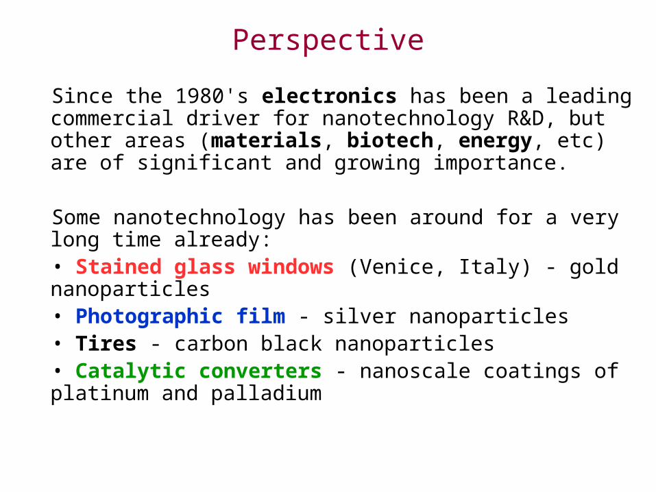
Since the 1980's electronics has been a leading commercial driver for nanotechnology R&D, but other areas (materials, biotech, energy, etc) are of significant and growing importance.
Some nanotechnology has been around for a very long time already:• Stained glass windows (Venice, Italy) - gold nanoparticles• Photographic film - silver nanoparticles• Tires - carbon black nanoparticles• Catalytic converters - nanoscale coatings of platinum and palladium
Perspective
QuickTime™ and aTIFF (LZW) decompressor
are needed to see this picture.
"Biggest science initiative since the Apollo program"
nano.gov

NSF Center for Hierarchical Manufacturing
Research Education Outreach
A Center on Nanomanufacturing at UMass
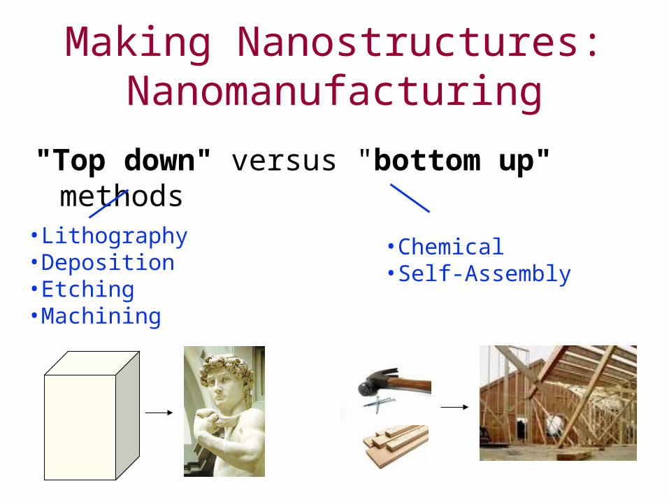
Making Nanostructures: Nanomanufacturing
"Top down" versus "bottom up" methods
•Lithography•Deposition•Etching•Machining
•Chemical•Self-Assembly

Photolithography for Deposition
substrate
process recipe
spin on resist
resist
expose
mask (reticle)
develop
deposit
liftoffnarrow line
apply spin bake
spin coating
exposed unexposed
"scission"
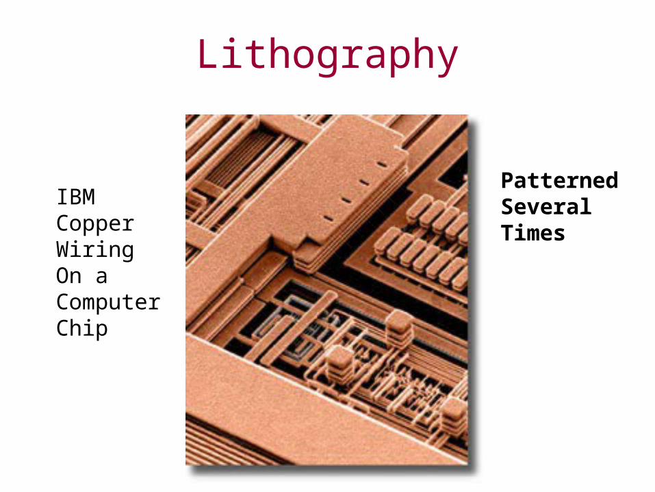
Lithography
IBMCopperWiringOn aComputerChip
PatternedSeveral Times
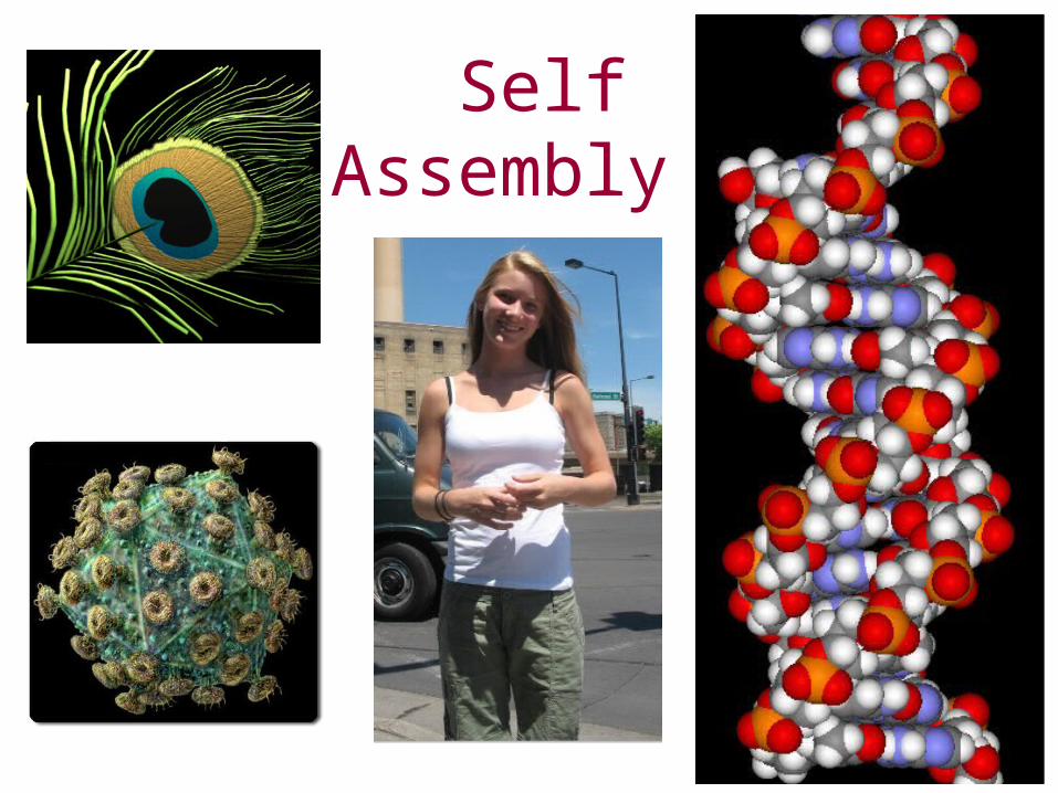
Self Assembly

An Early Nanotechnologist?
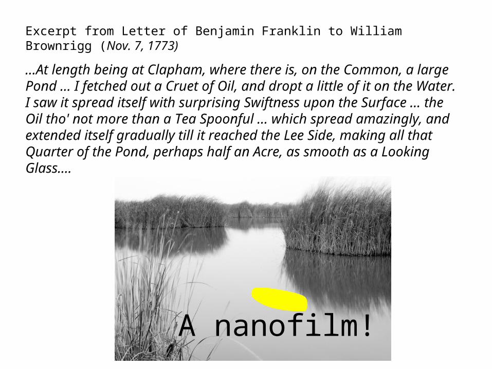
Excerpt from Letter of Benjamin Franklin to William Brownrigg (Nov. 7, 1773)
...At length being at Clapham, where there is, on the Common, a large Pond ... I fetched out a Cruet of Oil, and dropt a little of it on the Water. I saw it spread itself with surprising Swiftness upon the Surface ... the Oil tho' not more than a Tea Spoonful ... which spread amazingly, and extended itself gradually till it reached the Lee Side, making all that Quarter of the Pond, perhaps half an Acre, as smooth as a Looking Glass....
A nanofilm!
QuickTime™ and aTIFF (LZW) decompressor
are needed to see this picture.
QuickTime™ and aTIFF (LZW) decompressor
are needed to see this picture.
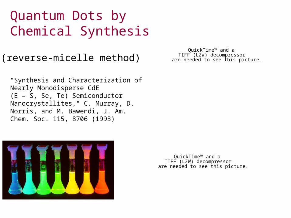
"Synthesis and Characterization of Nearly Monodisperse CdE(E = S, Se, Te) Semiconductor Nanocrystallites," C. Murray, D. Norris, and M. Bawendi, J. Am. Chem. Soc. 115, 8706 (1993)
Quantum Dots by Chemical Synthesis
(reverse-micelle method)

SELF ASSEMBLY with DIBLOCK COPOLYMERS
Block “A” Block “B”
10% A 30% A 50% A 70% A 90% A
~10 nm
Ordered Phases
PMMA PS
Scale set by molecular size
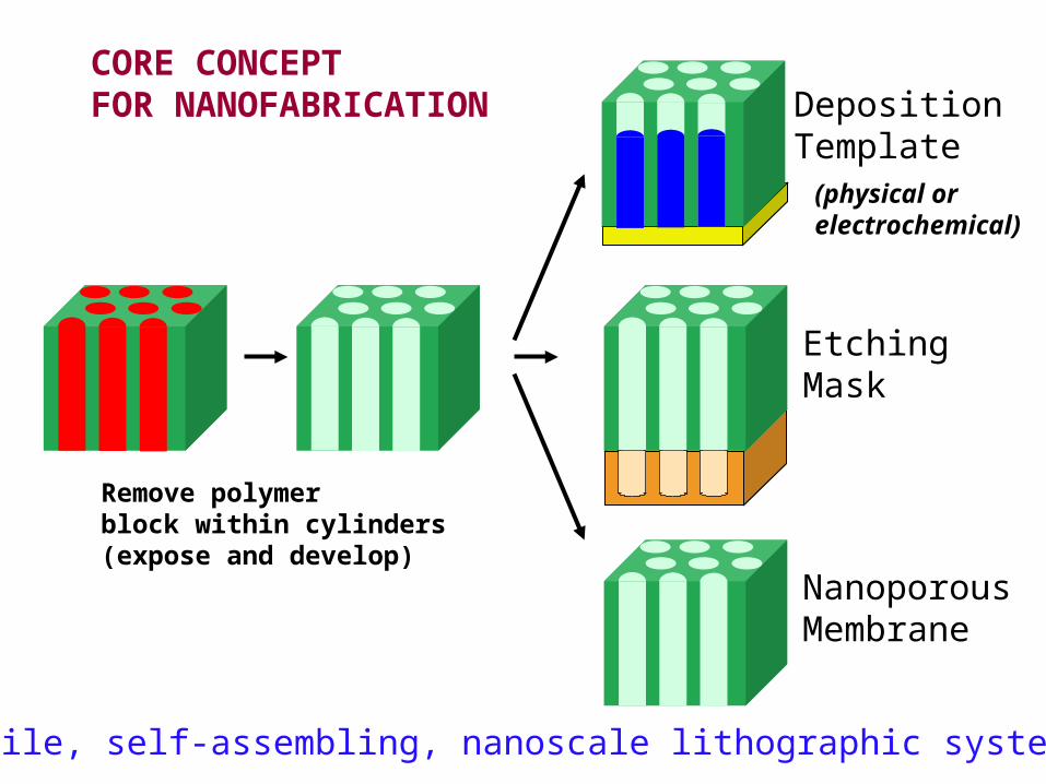
CORE CONCEPT FOR NANOFABRICATION Deposition
Template
EtchingMask
NanoporousMembrane
Remove polymerblock within cylinders(expose and develop)
Versatile, self-assembling, nanoscale lithographic system
(physical orelectrochemical)

nanoporous template
Nanomagnets in a Self-Assembled Polymer Mask
1x10¹² magnets/in2
Data Storage......and More

Why do we want to make things at the nanoscale?
• To make better products: smaller, cheaper, faster and more effective. (Electronics, catalysts, water purification, solar cells, coatings, medical diagnostics & therapy, and more)
• To introduce completely new physical phenomena to science and technology. (Quantum behavior and other effects.)
For a sustainable future!

Solar Cells
Konarka
Benefit: Sun is an unlimited source of electronic energy.

Perhaps the most important result of the Nanotechnology Initiative so far:
"The Medici Effect"
• Physics• Chemistry• Biology• Materials Science• Polymer Science• Electrical Engineering• Chemical Engineering• Mechanical Engineering• Medicine• And others
• Electronics• Materials• Health/Biotech• Chemical• Environmental• Energy• Food• Aerospace• Automotive• Security• Forest products
Students & Nanotechnology
- A Field for People Who Want to Solve Technological Challenges Facing Societies
Across the World