integrated ultrafast nonlinear optical devices in silicon thesis
TRANSCRIPT

INTEGRATED ULTRAFAST NONLINEAR OPTICAL DEVICES IN SILICON
Thesis by
Michael Hochberg
In Partial Fulfillment of the Requirements
for the Degree of
Doctor of Philosophy
California Institute of Technology
Pasadena, California
2006
(Defended May 10, 2006)

ii
Acknowledgments
This dissertation is the product of many years of effort, starting when I was a freshman.
My introduction to nanotechnology was taking APh 9, the introductory semiconductors
course at Caltech, taught by Professor Scherer. It takes a truly bold spirit to teach a
course where the first lab of the term combines exhausted Caltech upperclassmen as
teaching assistants, freshmen (who might be either apathetic or energetic, depending on
how much sleep they’ve had in the past week) as students, an acetylene cutting torch, and
hydrofluoric acid.
In my case, the exhausted teaching assistant was Tom Baehr-Jones. In our first lab
section, he cooked his arm with the cutting torch while sealing a quartz tube – I promptly
volunteered to try sealing mine next, undeterred by the smell of cooking meat wafting
from the hand he was hiding in his pocket. I’ve been working with Tom ever since. As it
turns out, his talents lie in other directions than working with acetylene torches: None of
this work would have been possible without the theoretical and modeling work that he’s
done over the past seven years. We’ve written nearly all of our papers together – he does
the theoretical work and electromagnetic design, and I build the devices and turn the
wrenches in the lab. His gift for coming up with new ideas and clever solutions to
intractable problems is unmatched in my experience. Some of the text and many of the
graphics in this dissertation are taken from the papers we’ve written together. Many
results of his derivations and theoretical work are included herein by reference.

iii
It would be hard to exaggerate the influence that Professor Scherer has had on me over
the years that I’ve worked in his lab. Being a member of his lab has been a defining
experience in my life. It’s hard to say what has made more of an impact on me – his
passion for new ideas and for trying things out, or the profound patience and tolerance
that he shows. His gift for giving his students enough guidance to find interesting
projects, and then providing both the intellectual space and the resources to follow the
project all the way through, is truly extraordinary. When I think of the generosity he’s
shown me during my time here at Caltech, I am at a loss for words to express my
gratitude to him.
On the subject of profound patience, I must also acknowledge Professor Theodore Doll,
who spent two years teaching me how to do science in the lab while he was a
postdoctoral scholar. Rube Goldberg would have been proud of some of the experiments
I put together when I was starting out.
There are many people who’ve contributed their ideas and their efforts to this line of
research. Chris Walker put together the original version of the test setup we use for our
planar optical testing in the Scherer Lab. Guangxi Wang, and more recently Michael
Shearn, have been of great help with the testing and fabrication of recent devices. Some
of the basic ideas and motivation associated with planar lightwave test and silicon optics
were first crystallized in collaboration with Dr. Cary Gunn while he was a graduate
student in the lab. I’ve had many productive discussions with Jeremy Witzens, Marko
Loncar, Mark Adams, Ilya Fushman, Dave Barsic, and Joerg Schilling. In addition, our

iv
collaboration with Boeing has been a productive one, and I would be remiss not to
mention the many discussions that I’ve had over the past several years with Dr. William
Krug and his team at Boeing Phantom Works. Our collaborators at the University of
Washington – Rhys Lawson, Phil Sullivan, Jingdong Liu, Jocelyn Takayesu, Professor
Alex Jen, and Professor Larry Dalton - who provided the polymer materials that are so
important for our nonlinear optics experiments, have made critical contributions to this
work. I’d particularly like to acknowledge the help of the staff and users of the Cornell
Nanofabrication Facility – Alan Bleier, Rob Ilic, Mike Skvarla, Daron Westly, and
Meredith Metzler in particular. If there’s one thing I learned at the CNF, it’s that
nanofabrication is the art of the possible.
The National Science Foundation, through its Graduate Research Fellowship, provided
financial support for me during the last three years.
This thesis is dedicated to my parents, Leonard and Martha Hochberg,
who taught me the meaning of quality work.

v
Abstract
Silicon-on-insulator (SOI) provides an intriguing system for developing massively
integrated optics. By leveraging the processes and systems developed for electronics
fabrication, it is possible to make highly repeatable devices where complexity can be
scaled up through the use of wafer-scale batch fabrication. Because the mode
concentration in silicon waveguides is two orders of magnitude higher than in fibers, it is
possible to construct very compact nonlinear optical devices within this system, enabling
the miniaturization and integration of ultrafast nonlinear devices. We have developed a
library of devices, including both dielectric and plasmonic waveguides, as well as
resonators, splitters, and a variety of other basic optical components.
Using these components to construct integrated devices of moderate complexity, we have
demonstrated Pockels’ Effect-based ring modulators, optical rectification-based
detectors, four-wave mixing devices, and ultrafast intensity modulators, which operate at
speeds in excess of 2 Terahertz. By integrating optical polymers through evanescent
coupling to high-mode-confinement silicon waveguides, the effective nonlinearity of the
waveguides can be greatly increased. The combination of high mode confinement,
multiple integrated optical components, and high nonlinearity produces all-optical
ultrafast devices operating at power levels compatible with modern continuous-wave
telecommunication systems. Although far from commercial modulator standards in
terms of extinction, these modulator devices are a first step toward large scale integrated
ultrafast optical logic in silicon, and are two orders of magnitude faster than existing free-
carrier-based silicon devices.

vi
\
© 2006 Michael Hochberg
All Rights Reserved

vii
Table of Contents
Chapter Title Page Number
1. Introduction 1
2. Passive Optical Devices 7
3. Plasmon Waveguides 18
4. Terahertz All-Optical Modulators 32
5. Second-Order Nonlinear Devices 56
6. Conclusion 91
Appendix A – Interesting Random Micrographs 93

viii
Figure Captions
Chapter 1 - Introduction
Chapter 2 - Passive Optical Devices
2.1 Cross-sectional view of an SOI wafer
2.2 Electric field vectors for a 500 nm by 100 nm silicon-on-insulator waveguide
2.3 Shallow-angle SEM view of a typical silicon-on-insulator ring resonator and
waveguide. Note that the sidewall roughness is on the order of 10 nm, and that
the silicon-insulator bond has been decorated with a brief buffered oxide etch.
2.4 Plan view of a ring resonator fabricated in SOI.
2.5 Typical high-Q resonance signature for clad and unclad resonators, with both
resonances centered at 0.
2.6 SEM image of a slot ring resonator directional coupler region, and associated
input waveguide.
2.7 SEM image of the top view of a segmented waveguide structure, in this case a
segmented and slotted waveguide.
2.8 (a) Dispersion diagram of both Series 0 segmented waveguide and the normal,
unsegmented waveguide. (b) Also shown are modal patterns of the Bloch mode,
with contours of |E| plotted, starting at 10% of the max value and with contour
increments of 10%. The first plot (a) is on a z plane that intersects the middle of a
segment. (c) shows a plot on a horizontal plane that intersects the silicon layer
halfway through. For clarity, four periods of the waveguide are shown.

ix
2.9 Slot waveguide mode converter with segmented waveguide region for electrical
isolation.
Chapter 3 - Plasmon Waveguides
3.1 Schematic representation of plasmon waveguide structure.
3.2 The SP waveguide geometry (a) is compared to the SOI waveguide geometry (b).
In both cases, contours of |E| are sketched, starting at 10% of the maximum value
and drawn for every increment of 10%. In (c), the effective index of the plasmon
mode is compared to that of the SOI waveguide mode as a function of
wavelength in micrometers.
3.3 Waveguide insertion loss (a) shows a diagram of the layout of a plasmon
waveguide length device, and (b) shows an SEM image of a fabricated device. (c)
shows the scatter plot and fitted line, as well as a scatter plot of the five best
calibration insertion loss structures for contrast. The axes are fiber to fiber
insertion loss in dB versus plasmon waveguide length in μm.
3.4 Straight waveguides. (a) and (b) are a rendering and an SEM image of a non-
defective waveguide. Panels (c) and (d) show a corresponding defective plasmon
waveguide. Panel (e) shows transmission spectra in dB for coupling through
several 2 μm long SP waveguides, as a function of free-space wavelength in
micrometers. The simulated transmission for this device is also shown. We
present the spectrum of the best SP waveguide device with a defect added for
comparison.
3.5 Renderings of plasmon waveguide bend used to demonstrate waveguiding
properties.

x
3.6 Device layouts and renderings from FDTD simulations are shown in (a) for the
non-defective, metal-free, and defective devices, clockwise from top left. The
out-of-plane H field is rendered as blue and red. In (b), the transmission spectra
of the best measured devices of each type are shown, with fiber to fiber insertion
loss in dB plotted against laser wavelength in μm. The baseline calibration loop
spectrum is also shown for comparison.
3.7 SOI to surface plasmon waveguide couplers. At left is a rendering of SOI
waveguides and SP waveguide bend with propagating plasmon mode. Also
shown at right is an SEM micrograph of a fabricated device.
3.8 Measured and simulated bent SP waveguide transmission. SEM images of a
normal (a) and defective (b) SP device with a bend radius of 0.25 μm. In (c), (d),
and (e) we show the measured and simulated transmissions for several 0.25, 0.5,
and 2 μm bends, respectively. The highest transmission of all the bend defect
devices are shown in all three for comparison.
Chapter 4 - Terahertz All-Optical Modulators
4.1 10% contours of the absolute value of the E field in a typical silicon waveguide
used in this work, clad with PMMA.
4.2 Negative result for FWM on a die coated only with PMMA
(polymethylmethacrylate), a material with no enhanced X3 properties. Typical
results, showing 40 dB of sideband extinction, are shown above.
4.3 Plot of device output after coating with JSC-1 polymer.
4.4 Graphic of modulator device layout.

xi
4.5 Graphic of the die layout and enlargement of the input region of the
interferometer.
4.6 Optical image of the input and output portion of a typical device, with
illustrations showing the flow of optical power.
4.7 Graphic showing Mach-Zehnder transmission spectrum as a function of
wavelength.
4.8 Layout of THz Experiment
4.9 Panels at top, left, and right show modulation of the source laser at 2.6 THz, 0.6
THz, and 0.25 THz, respectively. In the right panel, it is important to note how
the signal transmission changes with wavelength, while the modulation sideband
does not change in magnitude; this is the unmistakeable signature of an
amplitude modulator. Measurements at higher frequencies are difficult due to
bandwidth limitations of our test equipment and of our optical couplers, but we
predict that a device like ours will function at rates of 10 THz – the fundamental
limitation on such devices is dispersion in the waveguides.
4.10 Test data showing movement of sidebands with change in modulation frequency
from 0.5 nm to 20 nm spacing. The rolloff at high frequency is largely accounted
for by the reduction in coupler efficiency off-peak
4.11 Layout of the gigahertz modulation experiment
4.12 Shows the measured S-parameter for the device in various circumstances. The
red curve is the measured value of the S-parameter when both the gate and source
lasers are on. For control, we show the same measurement taken when the signal
laser is off, when the pump is off, and when all lasers are off, shown with the

xii
green, blue, and teal curves, respectively. The predicted S-parameter of -37 dB
from the dual gate experiment is also shown as a black line, and is found to be in
close agreement with the S-parameter measured.
4.13 Optical spectrum traces taken for various sinusoidal radio-frequency intensity
modulations on the gate. The intensity modulation of the gate laser results in
sidebands output, located near the source wavelength at the appropriate locations
for each input modulation frequency. The panel at right shows a detail of the
device output near the source wavelength for modulation at 10 GHz, 15 GHz, and
20 GHz.
Chapter 5 - Second-Order Nonlinear Devices
5.1 Illustration of the poling process.
5.2 Modal profile of the Silicon waveguide and the dispersion plot of a PMMA clad
waveguide. The profile is of |E|, with contour lines drawn in increments of 10%
starting at 10% of the maximum field value. The panel at right shows effective
index as a function of wavelength.
5.3 Normalized fiber to fiber transmission in dB as a function of wavelength in nm
for two different temperatures for one of the ring resonators studied. The
transmission has been normalized against our baseline fiber to fiber coupling
efficiency. A detailed plot of the peaks near 1498 nm is shown.
5.4 Panel at left shows dn/dλ versus wavelength in 1/nm, while the right panel lists
the simulated susceptibility to core changes, a dimensionless quantity as a
function of wavelength. In the bottom panel, we show the movement of a

xiii
resonance peak as a function of temperature offset, in degrees Celsius. The base
temperature was 20C. Also shown is the predicted behavior.
5.5 Micrograph of planar electrodes surrounding silicon waveguides, courtesy of
Boeing Phantom Works.
5.6 GDS file layout of 1x4x1 ROADM devices.
5.7 Data from a device measured at Boeing Phantom Works showing in excess of 3
full-width at half-max tuning.
5.8 Mode shape for an electrooptic-polymer-clad slot waveguide showing 10%
contours for electric field.
5.9 Device layout for testing shows electrodes, resonator, and optical couplers.
5.10 Images at various magnifications of the electrical contact structures used to
establish independent electrical contact to the inner and outer portions of the slot
ring resonators.
5.11 Images at various magnifications of the electrical contact structures used to
establish independent electrical contact to the inner and outer portions of the slot
ring resonators.
5.12 SEM images of FIB cross section show that gap is fully filled with polymers,
without void formation
5.13 Scanning electron micrographs of devices that failed electrically, after polymer
decoating in solvent.
5.14 Typical results for split-ring resonator tuning. In this case the polymer system
was YL/APC, and the poling conditions were 120C, 20V (outer ring positive), 12
minutes, voltage off after cooling to 30C.

xiv
5.15 Bit pattern generated by Pockels’ Effect modulation of a ring resonator at
approximately 6 MHz. Peak to valley extinction was approximately 13 dB. The
vertical axis represents input voltage and output power, both in arbitrary units.
Horizontal axis is time in microseconds. Voltage swing is on the input signal is
20 volts.
5.16 Results for a typical device operating at around 6 MHz.
5.17 Equivalent circuit of an optical rectification device
5.18 The data presented here is an exploration of the ability to reverse the polarity of
these devices by repoling, as a confirmation that the mechanism of current
generation is indeed optical rectification. Part a shows the dependence of the
steady state observed current after room-temperature biasing with various voltage
polarities for one device. The device was originally polled with a –12 V bias,
though at 110C. With one exception, applying a voltage in the direction of the
original polling voltage enhances current conversion efficiencies, while applying
a voltage against the direction of the polling voltage reduces the current
conversion efficiencies. The total power at the input to the devices for these
experiments was on the order of 1 mW.
Part b shows the behavior of several different devices immediately after thermal
polling or cycling without voltage. For each device, the table provides a “natural
history” going from top to bottom as the time passes. The only anomaly is the
third measurement on device 2; this was after many repeated tests on this device,,
and the current observed was substantially less than was observed in previous

xv
tests on the same device. Because this device was cycled repeatedly, we regard
this data point as being somewhat suspect, but include it for completeness.
5.19 Panel a shows the transmission spectrum of detector device 1, whereas b shows
detector device 2. Panel c shows several curves of current vs. power for three
measurement series. Series 1 is of the first device with the wavelength at 1549.26
nm, on a resonance peak. Series 2 is the first device with the wavelength at
1550.5 nm off resonance. Series 3 is for device 2, with the wavelength at 1551.3,
on resonance. Finally, panel d shows the output current as a function of
wavelength, overlaid with the transmission spectrum. The transmission spectrum
has been arbitrarily rescaled to show the contrast.
Chapter 6 - Conclusion
Appendix A – Interesting Random Micrographs

xvi
Papers Associated With This Work
Below is a list of my coauthored papers related to the work in this thesis. Short sections
of some of these papers have been used within this thesis in cases where the prose in the
papers did not bear any improvement.
Under Consideration at Nature Materials “Terahertz all-optical modulation in silicon-polymer
hybrid system.” M. Hochberg, T. Baehr-Jones, et al. Under Consideration, Nature Materials.
July 2005 “Segmented waveguides in thin silicon-on-insulator.” T. Baehr-Jones, M. Hochberg, C. Walker, J. Witzens, L. Gunn, A. Scherer. Journal of the Optical Society of America B: Optical Physics.
July 11, 2005 “Optical modulation and detection in slotted silicon
waveguides.” T. Baehr-Jones, M. Hochberg, et al., Optics Express 13 (14): 5216.
December 2005 “Analysis of the tuning sensitivity of silicon-on-
insulator optical ring resonators.” M. Hochberg, et al. IEEE/OSA Journal of Lightwave Technology.
Feb. 21, 2005 “High-Q optical resonators in silicon-on-insulator-
based slot waveguides.” T. Baehr-Jones, M. Hochberg, C. Walker, A. Scherer, Applied Physics Letters, 86 (8):
Nov. 1, 2004 “Integrated plasmon and dielectric waveguides.” M.
Hochberg, T. Baehr-Jones, C. Walker and A. Scherer. Optics Express, 12 (22): 5481-5486.
Oct. 18, 2004 “High-Q ring resonators in thin silicon-on-insulator.”
T. Baehr-Jones, M Hochberg, C. Walker, A. Scherer. Applied Physics Letters 85 (16): 3346-3347.
July 19, 2004 “Liquid-crystal electric tuning of a photonic crystal
laser.” B. Maune, M. Loncar, J. Witzens, M. Hochberg, T. Baehr-Jones, D. Psaltis, A. Scherer, and Y. Qiu. Applied Physics Letters, 85 (3): 360-362.
April 2004 “Mode matching interface for efficient coupling of light
into planar photonic crystals.” J. Witzens, M.

xvii
Hochberg, T. Baehr-Jones. Physical Review 69 (4): Art. No. 046609 Part 2: 1963-1968.
April 2004 “High quality factors and room-temperature lasing in a
modified single-defect photonic crystal cavity.” M. Loncar, M. Hochberg, A. Scherer, Y. Qiu. Optics Letters, 29 (7): 721-723.
Oct. 2003 “Photonic crystal waveguide-mode orthogonality
conditions and computation of intrinsic waveguide losses.” J. Witzens, T. Baehr-Jones, M. Hochberg, M. Loncar, A. Scherer. Journal of the Optical Society of America A: Optics, Image Science, and Vision, 20 (10): 1963-1968.
Patent Applications:
4/26/2005 Integrated Plasmon and Dielectric Waveguides Baehr-Jones, Tom Hochberg, Michael J Scherer, Axel 4/26/2005 Near Field Scanning Microscope Probes and Method for Fabricating Same Baehr-Jones, Tom Hochberg, Michael J Scherer, Axel 5/27/2005 Plasmon Waveguide Light Concentrators Baehr-Jones, Tom Hochberg, Michael J Scherer, Axel 6/7/2005 Segmented Waveguides Structures Baehr-Jones, Tom Hochberg, Michael J Scherer, Axel Walker, Chris I Witzens, Jeremy 11/15/2005 Coupled Segmented Waveguide Structures Baehr-Jones, Tom Hochberg, Michael J Scherer, Axel Walker, Chris I Witzens, Jeremy

xviii
6/17/2005 Split Ring Optical Cavities and Split Optical Cavities with Electrical
Connections Hochberg, Michael J Baehr-Jones, Tom Scherer, Axel 2/8/2006 Advanced Time-Multiplexed Etching Technique Hochberg, Michael J Baehr-Jones, Tom Scherer, Axel 6/17/2005 A Novel Geometry for the Detection of Optical Radiation Baehr-Jones, Tom Hochberg, Michael J 6/28/2005 Bremstrahlung Laser (BLASER) Hochberg, Michael J Baehr-Jones, Tom 6/28/2005 Quantum Dot Composite Laser Hochberg, Michael J Baehr-Jones, Tom 6/28/2005 ICP PECVD Deposited Layers as a Protective Cladding for Polymer-Based
Devices Hochberg, Michael J Baehr-Jones, Tom Scherer, Axel 6/28/2005 Frequency Conversion with Nonlinear Optical Polymers and High Index
Contrast Waveguides Hochberg, Michael J Baehr-Jones, Tom 8/31/2005 Ultrafast Optical Modulator Hochberg, Michael J Baehr-Jones, Tom

1
1. Introduction
Organization and Content of This Work
The work described in this thesis was organized into two primary efforts. The first effort
was the construction of a library of optical components in silicon-on-insulator. These
included waveguides, resonators, splitters, couplers, and so forth. The critical feature of
these devices is that they all shared the same substrate and the same fabrication process,
so that they could be integrated together in order to construct more complex systems. As
it turned out, some of the individual structures were sufficiently novel to be publication-
worthy by themselves. The second effort involved using these structures in order to
construct integrated nonlinear optical devices.
The resulting structures and devices were published in a number of papers, some with
myself and some with Tom Baehr-Jones as the first author. This reflects an arrangement
we reached when we arrived in graduate school that we would alternate authorship on our
papers in cases where shared first-authorship was not an option. The reason for this
arrangement is simple: The tasks of experiment design, optical simulation and simulation,
software development, device fabrication, equipment maintenance, device test, data
analysis, and paper writing were simply too much for a single person to do. We believed
that having an equal stake in the outcome of the projects would ensure both transparency
and efficiency in our collaboration.
Tom Baehr-Jones was responsible for device design, software development, and much of
the data analysis in these experiments. I constructed the devices, coordinated contact

2
with other students and outside groups, and dealt with the lab side of things.
Experimental conception and design was generally shared, and the actual devices we
ended up building were most often the product of interactions between me and Baehr-
Jones.
The content of this thesis closely tracks the content of several of our papers. In many
cases the figures used herein have been taken from the papers themselves. In instances
where I could not improve upon the prose in the published papers, paragraphs and short
sections have been taken whole. In particular, figure captions are often reused, as they
are both as precise and as concise as I could manage and I could see no way to improve
them.
The first chapter of this thesis describes some of the most important examples of the
library of optical components that we developed. The second regards plasmon devices
that were constructed so that they could be integrated with silicon waveguides. The
remainder, which consists of two chapters, describes the nonlinear devices we’ve built –
first about those based on third-order effects and the second about those utilizing second-
order nonlinearities.

3
Integrated Photonics in Silicon
The last few years have seen an explosion of interest in integrating multiple optical
components onto the same chip.1 This interest is driven by a stark economic reality:
Much of the cost and complexity of building optical components for telecommunications
is often in their packaging; optical alignments of multiple fibers can be very nontrivial,
and there has been substantial interest in making multiple optical components on the
same chip for some years.2 The chips themselves are very often a small fraction of the
finished cost of a completed optical component.
One reason for the high cost of single-mode fiber optic components such as lasers and
modulators is that packaging each of these devices almost always requires that the device
be cleaved and then that a fiber be attached to it in order to extract the light.3 This
process is inherently serial and is difficult to automate inexpensively, since even in the
simplest cases it requires a 4- or 5-axis optical alignment between fibers. This alignment
and packaging is a low-yield process, and often results in the failure of many of the
devices. Even worse, it is usually not possible to test the devices until this packaging has
occurred, so many improperly fabricated, defective devices are packaged before their
failure can be determined.
This situation is even worse in the case of devices that have multiple inputs and outputs –
these either require several alignments or make use of fiber arrays, which often cost as
much as $100 per fiber,4 So the cost of these devices, which are typical of single-
function optical components today, is largely driven by the costs of packaging the

4
devices. This is, in large part, the impetus behind the current interest in integrating
multiple optical components into the same package; if the packaged chip can have the
same number of optical connectors but replace several less-complex components that
have to be packaged separately, the economics of such a device rapidly become very
compelling.
Many of the most important optical devices today are those where this disastrous testing
situation is alleviated by the device design itself. For instance VCSELS, originally
developed by Professor Axel Scherer at Bell Labs, allow tests to occur before packaging
and do not require wafer cleaving, since they are coupled out of plane. VCSELS are
limited to relatively low output power, because of their very short gain regions; many
research groups and companies are working, for instance, on the construction of grating-
coupled surface emitting lasers (GCSELS) that will combine some of the advantages of
VCSELS with the high output power of in-plane laser structures.5
The benefits of integration for photonic devices are obvious. With costs and yields that
are often driven by packaging, being able to integrate more than one optical function (for
instance having multiple modulators, and combining several different wavelengths
together through a mux) into the same chip can give very substantial advantages.
Furthermore, there is substantial supporting electronic circuitry required in order to make
even simple photonic devices work properly – lasers require drivers; arrayed waveguide
gratings can require fine-grained thermal control circuitry; along with taps and detectors
for closed-loop feedback; high-speed detectors require trans-impedance amplifiers, and

5
so on. Being able to integrate optics with the supporting electronics is one of the driving
forces behind work currently being done in silicon integrated optics at places like
Luxtera,6 where the author of this work was a cofounder. Luxtera has demonstrated
integrated 10G transmitters and receivers in a standard foundry silicon process.
So given the ability to demonstrate and then manufacture large scale integrated optical
devices in standard, electronics-compatible foundry silicon, we found ourselves asking a
couple of questions: Is there novel physics that this platform makes accessible? Are
there novel devices that this kind of integration makes accessible, beyond integrating the
components that already exist as discrete devices together onto the same chip?
One idea that we found intriguing and chose to investigate was the notion of using these
integrated optical systems in silicon for ultrafast nonlinear optics. The nonlinear activity
of silicon is fairly negligible, but as it turns out it is possible to construct waveguides that
simultaneously provide two different advantages: First, they concentrate the optical
mode field into areas on the order of .5 square microns – this is between two and three
orders of magnitude smaller than what is achieved in single-mode fibers. Second, the
mode can be forced to exist in large part outside the high-index waveguide core, where it
can be evanescently coupled to highly active nonlinear polymers in order to increase the
nonlinear optical activity of the system.
Some work has been done on all-silicon nonlinear optical devices, but these devices
generally either exhibit fairly weak nonlinear response, or are based on two-photon

6
absorption and free-carrier plasma effects.7 Since the free-carrier devices are limited by
diffusion times, their speed is limited to the gigahertz regime. With the approach we
have taken, we are able to take advantage of the high field concentration,
manufacturability, and compactness of nanoscale silicon waveguides at the same time as
we gain the benefits of the latest high-activity nonlinear optical polymers. The
engineering of such polymers has been an active field over the past several years, and
polymers have been developed that exhibit strong nonlinear effects that are both second-
and third-order. In addition, such polymers have been demonstrated to have response
characteristics that extend into the ultrafast frequency regime.89
In this work, I show results both for the individual optical devices that we’ve constructed
in silicon-on insulator, and for some of the integrated ultrafast nonlinear optical devices
that we’ve constructed using the hybrid silicon/polymer material system.
1 M. Lipson., “Guiding, modulating, and emitting light on silicon – Challenges and opportunities.” J. Lightwave Technology 23 (12): 4222, 2005. 2 T. Koch, “Semiconductor Photonic Integrated Circuits”, IEEE J. Quantum Electronics 27 (12): 641, 1991. 3 N. Kashima, “Passive Optical Componoents for Optical Fiber Transmission.” Norwood, MA: Artech House, 1995. 4 Conversations with Oz Optics, Inc., PLC Connections LLC. 5 JL Jewell, JP Harbison, A. Scherer, et al. ”Vertical-Cavity Surface Emitting Lasers – Design, Growth, Fabrication, Characterization.” IEEE J. Quantum Electronics 27: (6) 1332, 1991. 6 www.luxtera.com 7 Q.F. Xu, M. Lipson. “Carrier-induced optical bistability in silicon ring resonators.” Optics Letters 31 (3): 341, 2006. 8 X. Y. Hu, Y. H. Liu, J. Tian, B. Y. Cheng, D. Z. Zhang. “Ultrafast all-optical switching in two-dimensional organic photonic crystal.” Appl. Phys. Lett. 86, 121102 (2005). 9 A. Nahata, D. H. Auston, C. J. Wu, J. T. Yardley, “Generation of Terahertz Radiation From a Poled polymer,” Appl. Phys. Lett., 67, 1358 (1995).

7
2. Passive Optical Devices
In order to enable the construction of optical circuits for doing integrated nonlinear
optics, it was critical first to construct a set of different optical components in a common
material system. There are many options in terms of different types of silicon-on-
insulator from which to choose for doing integrated optics. Our parameters for choosing
our layer thickness were driven largely by two factors: First, it was desirable for the final
structure to be fundamentally compatible with the types of planar batch fabrication that
are commonly used for silicon electronics processes. Second, we wanted a structure that
would allow for high field concentration, low loss, and high interaction with cladding
material.
On the subject of compatibility with electronics, there are a number of options. For
electronics purposes, there are two competing alternatives for making devices – bulk
silicon and silicon-on-insulator (SOI).12 From the standpoint of optics, it would be very
hard to construct optical waveguides in plain silicon wafers; achieving vertical
confinement and preventing light from leaking into the substrate would be very
challenging, if not impossible, due to the extremely high index of silicon.
In SOI, there has been extensive work done3 in making micro-electro-mechanical-
systems-compatible waveguides over the last several years. Unfortunately, the SOI that
is typically used for MEMS applications has a very thick top silicon layer, on the order of
tens of microns or more. As a result, making single-mode optical waveguides in such a
system is often achieved by doing a very shallow etch into the silicon, in order to achieve

8
a low lateral index contrast and a large mode size. Such a large mode, although it can be
very low loss, is not particularly attractive for nonlinear optical applications, where a
high field concentration, and thus a very compact optical mode, is extremely desirable.
Additionally, such waveguides are of limited utility for integrating multiple devices onto
the same chip, since they exhibit very large bend radii for low-loss waveguide bends.
A brief inspection of the ITRS Roadmap4 shows that top silicon layer thicknesses for
modern electronics-grade SOI have already dropped below 100 nm. To use anything that
looks much like an electronics-compatible silicon wafer, it’s necessary to start with SOI
having top silicon layer thicknesses on the order of 100 nm.
Figure 2.1: Cross-sectional view of an SOI wafer.
In terms of achieving high field concentration, the obvious choice is to work with
whatever waveguides achieve the smallest convenient mode volumes and offer low loss.
One option that provides very high mode field concentration is to work with fully etched,
thin silicon-on-insulator. Of course in an electronics process the bottom oxide is
typically quite thin5, and such a thin oxide would result in devastating substrate leakage
Silicon (TOPSI)
Oxide (BOX)
Silicon Substrate

9
from any reasonable waveguide. In our work, the starting material was 100-120 nm thick
top silicon on oxides that varied for the various experiments between 1.4 and 3 microns.
As it turns out, it is possible to design highly confined optical waveguides in this material
system, with extremely compact optical modes in the 1550 nm telecommunications band.
The typical waveguides used in this work were on the order of 500 nanometers wide, and
were fully etched to the bottom oxide.
Figure 2.2: Electric field vectors for a 500 nm by 100 nm silicon on insulator waveguide
These waveguides have an additional benefit; to wit there is substantial interaction with a
cladding material above the oxide. We take advantage of this for work described in
ensuing chapters on nonlinear optical devices, where these waveguides are clad with
highly active nonlinear optical polymers. For this waveguide, 57% of the optical power
is localized outside the waveguide core, where it can be made to interact with cladding
materials (assuming that the silicon dioxide supporting layer can be largely undercut).

10
High-Q Ring Resonators in Thin Silicon-on-Insulator
One of the first results achieved with these thin SOI optical resonators was the
construction of high-Q microresonators based on low-loss single-mode waveguides.
These were based upon 120 nm thick and 500 nm wide silicon nano-waveguides.
Figure 2.3: Shallow-angle SEM view of a typical silicon-on-insulator ring resonator and
waveguide. Note that the sidewall roughness is on the order of 10 nm, and that the
silicon-insulator bond has been decorated with a brief buffered oxide etch.

11
Figure 2.4: Plan view of a ring resonator fabricated in SOI
The losses of such systems are generally attributable to some combination of three
possible mechanisms – (1) absorption in the material, (2) scattering, and (3) substrate
leakage. In the case of these waveguides, the material absorption of silicon was not a
limiting factor, since the losses of silicon at telecom wavelengths are quite small.6
Substrate leakage for this thickness of oxide layer was found through perturbation theory
to be between 3 and 4 dB per centimeter. Through extensive optimization of lithography
and etching conditions, we were able to bring the total waveguide losses down to about
6.6 dB/cm for PMMA-clad resonators, and to 7.1 dB/cm for unclad ones. This
corresponded to maximum uncoupled resonator Q values of 94,000. By reducing the
optical losses through the use of a 3-micron-thick oxide, losses were later reduced to less
than 3dB/cm. We attribute the majority of the remaining waveguide loss to edge-
roughness induced scattering and to absorption losses.

12
Figure 2.5: Typical high-Q resonance signature for clad and unclad resonators, with both
resonances centered at 0.
Although these results have been surpassed since they were published, with some groups
showing disk resonators with Q values in excess of 1,000,000 in silicon,7 these results
were, at the time of publication, the highest Q values for single mode silicon-on-insulator
ring micro-resonators.
These devices were fabricated using a Leica EBPG 5000+ 100 kV electron beam
lithography system. The resist system used for these, and all other waveguides described
in this work, was a Dow-Corning hydrosequisiloxane negative tone electron beam resist.8
Etching was performed using a chlorine-based inductively coupled plasma reactive ion
etcher, and optical testing was done using a highly automated fiber-array-based out-of-
plane optical testing system. This system is capable of performing a single-mode optical
fiber alignment and wavelength sweep to characterize a device in a couple of minutes.
13
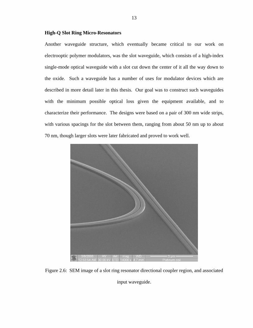
High-Q Slot Ring Micro-Resonators
Another waveguide structure, which eventually became critical to our work on
electrooptic polymer modulators, was the slot waveguide, which consists of a high-index
single-mode optical waveguide with a slot cut down the center of it all the way down to
the oxide. Such a waveguide has a number of uses for modulator devices which are
described in more detail later in this thesis. Our goal was to construct such waveguides
with the minimum possible optical loss given the equipment available, and to
characterize their performance. The designs were based on a pair of 300 nm wide strips,
with various spacings for the slot between them, ranging from about 50 nm up to about
70 nm, though larger slots were later fabricated and proved to work well.
Figure 2.6: SEM image of a slot ring resonator directional coupler region, and associated
input waveguide.

14
Ring resonators were built using these waveguides, and the devices were characterized
for their optical loss performance. Q values of 27,000 were observed for these
resonators, corresponding to optical losses of approximately 10 dB/cm. These results
were for a resonator with 50 microns radius.
Segmented Waveguide Structures
In addition to being able to guide light, it was desirable to be able to form both electrical
contacts to waveguides and structures that would provide electrical isolation with low
optical loss. One approach to the construction of such devices is the use of high-index
segmented waveguide structures, which consist of a central waveguide portion with
ridges sticking out to the sides. With the light localized in the center in a Bloch mode,
electrical contact can be established using the “fins” that stick off the sides of the
waveguide.9

15
Figure 2.7: SEM image of the top view of a segmented waveguide structure, in this case
a segmented and slotted waveguide.
Through a combination of optical design using a Hermetian Bloch mode eigensolver and
iteration through many possible structures in the lab, it was found that (non-slotted)
segmented waveguide structures could be constructed in 120 nm thick SOI. Waveguide
losses as good as -16 dB per centimeter were observed, and insertion losses as good as
-.16 dB were shown from standard silicon waveguides.10
Figure 2.8: (A) Dispersion diagram of both Series 0 segmented waveguide and the
normal, unsegmented waveguide. (B) Also shown are modal patterns of the Bloch mode,
with contours of |E| plotted, starting at 10% of the max value and with contour
increments of 10%. The first plot (A) is on a z plane that intersects the middle of a

16
segment. (C) shows a plot on a horizontal plane that intersects the silicon layer halfway
through. For clarity, four periods of the waveguide are shown.
Finally, we wanted to be able to construct structures that would provide electrical
isolation without substantial optical loss. By utilizing the same type of design
methodology as was used for the segmented waveguides, electrical isolators such as those
shown below were constructed, which provided both a transition from a standard to a
slotted waveguide and electrical isolation between the two sides of the slot waveguide.
Such structures were shown to have losses on the order of .5 dB.
Figure 2.9: Slot waveguide mode converter with segmented waveguide region for
electrical isolation.
17
1M. Lundstrom. “Moore’s Law Forever?” Science 299, 210 (2003). 2 ITRS 2005 Roadmap. http://www.itrs.net/Common/2005ITRS/Home2005.htm 3 W. Noell et al. “Applications of SOI-based optical MEMS.” IEEE J. of Selected Topics in Quantum Electronics, 8 (1) 148 (2002). 4M. Hoffman, E. Voges. “Bulk Silicon micromachining for MEMS in optical communication systems.” J. Micromechanics and Microengineering 12, 349 (2002). 5 ITRS 2005 Roadmap. http://www.itrs.net/Common/2005ITRS/Home2005.htm 6 R. A. Soref, J. P. Lorenzo, “All-Silicon Active and Passive Guided-Wave Components For Lambda=1.3 and 1.6 MU-M,” IEEE J. Quantum Electron. 22, 873-879 (1986). 7 M. Borselli, T. J. Johnson, and O. Painter, "Beyond the Rayleigh scattering limit in high-Q silicon microdisks: theory and experiment," Opt. Express, Vol. 13, No. 5, pp. 1515-1530 (2005). 8 H. Namatsu et. al. “Three-dimensional siloxane resist for the formation of nanopatterns with minimum linewidth fluctuations.” Journal of Vacuum Science and Technology B 16 (1), 69-76 (1998). 9 J. Witzens, T. Baehr-Jones, M. Hochberg, M. Loncar, and A. Scherer, "Photonic crystal waveguide-mode orthogonality conditions and computation of intrinsic waveguide losses," J. Opt. Soc. Am. A 20, 1963-1968 (2003) 10J. Witzens, T. Baehr-Jones, M. Hochberg, M. Loncar, and A. Scherer, "Photonic crystal waveguide-mode orthogonality conditions and computation of intrinsic waveguide losses," J. Opt. Soc. Am. A 20, 1963-1968 (2003)

18
3. Plasmon Waveguides
It is well known that all dielectric waveguides are fundamentally limited in terms of the
field concentration that can be achieved by diffraction.1 For nonlinear optics, the field
concentration is the primary limitation on how small active devices can be made – higher
field concentrations result in smaller devices. As a result, any technique that would allow
light to be guided in modes that are smaller than those provided by diffraction-limited
optics would be extremely interesting for applications in nonlinear optics. One such
method for guiding light is the use of surface plasmons. More properly called surface
plasmon polaritons, plasmons propagate on the surfaces of metals and are optical modes
that propagate partially as a charge wave on the surface of that metal. Since the light is
guided outside of the metal, it seemed that these might be an ideal structure for nonlinear
optics, since they could in principle provide a very high mode overlap with any cladding
material. An additional attraction of such waveguides is the ability to use the metal as
an electrode; for instance, for adding bias voltage or radio-frequency signal to the active
region of an optical device.
Because of the largely imaginary index of refraction of the metals in question – in this
case silver – such modes are intrinsically quite lossy, and there is not likely to be an
engineering solution that fixes this, since the imaginary component of the index of
refraction is critical for supporting the guiding of such modes.2
The plasmon modes that were of interest for our work were those that exhibited relatively
high mode field concentrations, since this kind of guiding is desirable for our nonlinear

19
optics work. In addition, we wanted modes where we could relatively easily couple from
our standard silicon-on-insulator structures, so that we could take advantage of the
substantial existing infrastructure we had developed for coupling and manipulating light
on-chip. Of course, the structures needed to be amenable to planar batch fabrication.
There has been extensive work over the past several years on various geometries of
plasmon waveguides. These range from work on nanoscale waveguides with extremely
compact modes3 to ones where the guiding is extremely weak and the mode size is
comparable to that of a fiber.4 These two cases basically span an enormous space in
terms of mode size and a wide variety of different waveguide designs have been
explored; the trend clearly indicates that high loss and high mode concentration appear to
be inextricably linked across different geometries.
We found that although a very high optical field concentration can be achieved with
plasmon waveguides, there is a high optical loss coupled to the high mode field
concentration. As a result, the waveguides were found to be largely impractical for
nonlinear optical applications, given that conventional dielectric waveguides are
substantially less lossy than these plasmon guides and are substantially easier to fabricate
and test with the equipment available to us. However, the existence of plasmon guiding
in the novel system we developed and the ability to couple nanoscale plasmon
waveguides to standard silicon optical waveguides is of some intrinsic interest, as the
existence of the plasmon modes we exploited is not prima-facie an obvious conclusion.

20
Device Results
The design work for these structures was carried forward by Tom Baehr-Jones, using his
finite-difference time domain code and Hermetian eigensolvers.5 The designs that were
explored centered upon guiding of electromagnetic radiation at the edges of a planar
deposited layer of silver. A number of metals were explored, and silver was found to
minimize the optical losses of the system.
Figure 3.1: Schematic representation of plasmon waveguide structure.
Active
Oxide
Silicon Handle
Cladding
Metal

21
The plasmon waveguides consisted of 100 nm of electron-beam deposited metal, sitting
on an oxide layer next to our standard silicon waveguides. This structure presented
substantial fabrication challenges, since the alignment between the two lithographic
layers needed to be better than 50 nm. At the time of this work, we were just setting up
our new 100 kV electron-beam lithography system, and a number of problems cropped
up in getting the interlayer alignment within tolerances for these devices. Many of these
problems were eventually traced to thermal instabilities in the cleanroom where the
electron beam system was located, which resulted in stage instabilities for the electron
beam system. We chose to deal with some of these problems through a zebra-mask
strategy, where multiple devices were fabricated with built-in layer offsets, in order to
end up with a subset of the devices fabricated to the design specifications.
Device fabrication began with our standard waveguide fabrication process. Beginning
with clean SOI wafers of 120 nm silicon on oxide, HSQ resist was spun onto the chip,
baked at 170C, and exposed at 100kV and 3500 uC/cm^2. Patterns, which included
alignment marks for automated alignment of the following layers, were etched into the
silicon using a chlorine-based ICP-RIE process.67 The metal lithography was performed
in PMMA, and the metal layers were lifted off in order to ensure the best possible edge
quality. The deposition was performed in an electron-beam evaporator at the highest
available rate – on the order of several nanometers per second – in order to keep the
sample heating and grain size to a minimum. Finally, the entire chip was coated with a
thick layer of PMMA, which prevented tarnishing of the silver and provided an optical
cladding. The samples were generally kept under a vacuum for shipping and storage.

22
Figure 3.2: The SP waveguide geometry (a) is compared to the SOI waveguide geometry
(b). In both cases, contours of |E| are sketched, starting at 10% of the maximum value and
drawn for every increment of 10%. In (c), the effective index of the plasmon mode is
compared to that of the SOI waveguide mode as a function of wavelength in
micrometers.

23
For these plasmon waveguides, the peak electric field for a milliwatt of input power turns
out to be about 3x10⁶ V/m; this is not substantially different from the peak fields
generated in our silicon-only waveguides. Our hope was that perhaps we could use these
plasmon waveguides as an initial stage that would couple into more-highly-confined
plasmon waveguides, though we never ended up implementing those designs due to the
difficulty of fabricating the plasmon devices.
The first type of device that we fabricated consisted of straight plasmon waveguide
lengths of varying plasmon propagation lengths, ranging from 2 to 12 μm.. Light was
coupled into and out of the SOI waveguides from a polarization-maintaining fiber array
employing standard coupling geometries.8 An input laser was swept in wavelength at -3
dBm laser power to characterize each device, in increments of 0.01 nm. We were able to
effectively measure the device responses for free-space wavelengths from 1.5 to 1.53 μm,
a bandwidth range that nearly encompasses a fiber-optic telecommunications band.
Baseline calibration loops, which consisted of simple SOI waveguide loops with no
plasmon devices, were used to measure the base insertion loss of the test setup and fiber
to SOI waveguide coupler performance.
As predicted, the frequency response of our devices was fairly flat in the 1.5-1.53 μm
regime. Taking the peak transmission in the 1.51 μm to 1.52 μm spectral region for the
best 5 devices of about 150 devices fabricated for each length, we performed a linear
regression to identify the coupling insertion loss and propagation loss of the plasmon

24
waveguide. These values were found to be 4.2±1.6 dB and 1.3±.4 dB/μm, respectively.
The best device measured demonstrated 3.4±.4 dB of coupling insertion loss. The
coupling efficiency measured was found to be in agreement with the predicted value from
FDTD, while the propagation loss is clearly higher in the plasmon waveguide; this is
most likely a result of fabricated imperfections in the silver slab edge. The fitted line, and
a scatter plot of this data are shown in figure 3.3. The error scatter in the data is not quite
Gaussian, likely due to our use of a zebra-mask strategy to deal with misalignments
between the lithography layers.
There is substantial coupling between the silicon waveguides in the absence of any
metal structure. Because of the high absorption of the plasmon waveguides, the loss from
free-space coupling is similar to the losses from the plasmon waveguides, and thus a
comparison of straight waveguide devices with and without metal structures does not
provide compelling evidence of plasmon guiding. Our simulations, however, show that
the free-space mode is completely disrupted by the addition of the metal structure.
Furthermore, with the addition of 1 um x 1um defects sticking out of the metal (similar to
those shown below for the bend devices), the plasmon mode is completely disrupted. The
extinction measurements with these defects added were limited by the noise floor on the
measurement setup, giving an overall extinction consistently in excess of 10 dB between
devices with the defect and those without. Because of the high degree of localization of
the defect, it would not be expected to greatly attenuate free-space coupling. However,
such defects were found in simulations to completely disrupt the transmission of the
plasmon mode. Because of the good coupling in the absence of the metal, these
structures do not provide compelling evidence for plasmon guiding, but with the bend

25
data to confirm the guiding and the coupling, can be legitimately used to characterize the
waveguide losses.
Figure 3.3: Waveguide insertion loss. A) shows a diagram of the layout of a plasmon
waveguide length device, and B) shows an SEM image of a fabricated device. C) shows
the scatter plot and fitted line, as well as a scatter plot of the five best calibration insertion
loss structures for contrast. The axes are fiber to fiber insertion loss in dB versus plasmon
waveguide length in μm.
In Figure 3.4, we show the transmission spectrum of the best four measurements on 2 μm
plasmon waveguide segments connecting two silicon waveguides. We normalized our
raw transmission data against the average transmission spectrum of the control structures
without metal waveguides to obtain these spectra. A wavelength-independent uncertainty
of 2.6 dB is typically observed in these experimental measurements due to lithographic
variations in our fiber couplers connecting the SOI chips to the measurement system. We

26
also show model predictions of coupling efficiencies for a straight waveguide segment
with the SP couplers described above. Finally, the transmission data from the best
measured defective SP waveguide device is shown in the same plot and a high extinction
is observed in waveguides with defects. The extinction measurements from defective
devices were limited by the optical noise floor of our detectors. This indicates that a
surface plasmon mode transports the optical energy.
Figure 3.4: Straight waveguides. (a) and (b) are a rendering and an SEM image of a non-
defective waveguide. Panels (c) and (d) show a corresponding defective plasmon
waveguide. Panel (e) shows transmission spectra in dB for coupling through several 2
μm long SP waveguides, as a function of free-space wavelength in micrometers. The
simulated transmission for this device is also shown. We present the spectrum of the best
SP waveguide device with a defect added for comparison.
Naturally, we wished to confirm that plasmon guiding was actually occurring, as opposed
to free-space coupling between the silicon waveguides. Curved plasmon waveguide

27
devices were fabricated, which utilize tight plasmon waveguiding to achieve small bend
radii. These devices were fabricated with the plasmon-dielectric couplers detailed above,
and with bend radii of 0.5 μm. In figures 3.5 and 3.6, we show the plasmon bend device,
a plasmon bend device with a defect added, and a device with no metal layer. We also
show renderings of the FDTD simulations, as well as the simulation results. Finally, we
show the measured data from fabricated devices. We have chosen the best device
measurements, selected from about 25 devices of each type. For transparency, we show
the raw data measured, as well as the test setup baseline curve, which is the fiber to fiber
insertion loss for a simple SOI waveguide calibration loop.
Figure 3.5: Renderings of plasmon waveguide bend used to demonstrate waveguiding
properties.

28
Figure 3.6: Device layouts and renderings from FDTD simulations are shown in A, for
the non-defective, metal-free, and defective devices, clockwise from top left. The out-of-
plane H field is rendered as blue and red. In B), the transmission spectra of the best
measured devices of each type are shown, with fiber to fiber insertion loss in dB plotted
against laser wavelength in μm. The baseline calibration loop spectrum is also shown for
comparison.
The ripple observed in the spectra is due to return losses on-chip and on our input
couplers forming cavities. FDTD simulations predict that the 0.5 μm bend device should
have 11 dB of insertion loss in the 1.5-1.53 μm range, while the defect introduces 16 dB
of loss for the entire bend. Perhaps more importantly, a complete absence of a metal layer
induces an insertion loss of 25 dB. The measured device performance is in approximate
agreement with these values, when the testing noise floor of -55 dB is taken into account.
Note that the nearly 15 dB extinction observed in the bend calibration device is closer to

29
the simulated value of 11 dB, since the propagation loss of the plasmon waveguide is
about .9 dB/μm above the simulated value, most likely due to edge roughness.
Figure 3.7: SOI to surface plasmon waveguide couplers. At left is a rendering of SOI
waveguides and SP waveguide bend with propagating plasmon mode. Also shown at
right is an SEM micrograph of a fabricated device.
30
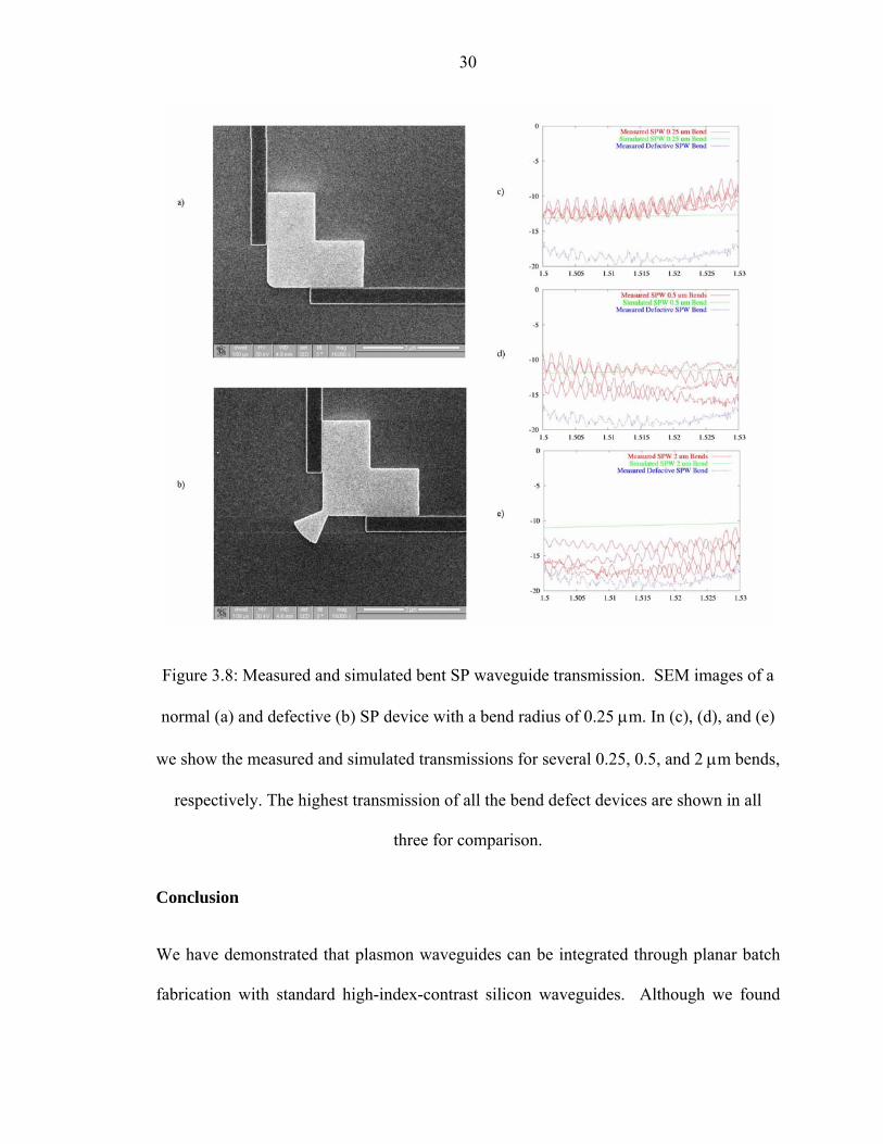
Figure 3.8: Measured and simulated bent SP waveguide transmission. SEM images of a
normal (a) and defective (b) SP device with a bend radius of 0.25 μm. In (c), (d), and (e)
we show the measured and simulated transmissions for several 0.25, 0.5, and 2 μm bends,
respectively. The highest transmission of all the bend defect devices are shown in all
three for comparison.
Conclusion
We have demonstrated that plasmon waveguides can be integrated through planar batch
fabrication with standard high-index-contrast silicon waveguides. Although we found

31
that these plasmon waveguides were not of great utility in our continued work on
nonlinear optics, it is possible that they will find use in sensing or nonlinear optical
applications in the coming years, as they provide a mechanism to transition from a
diffraction-limited optical mode to one that is not limited by diffractive optics. It may be
that, for instance, by quickly tapering from plasmon waveguides like the ones
demonstrated here into much higher-confinement waveguides, it will be possible to
explore optics where modes are compressed by orders of magnitude from their free-space
wavelength, and are thus extremely highly confined. In addition, we are optimistic that
these plasmon waveguides might find applications in metrology, where the high mode
field concentrations at their corners might be used as probe tips for SPM and NSOM
applications.
1 B. Saleh, M. Teich. “Fundamentals of Photonics.” New York, John Wiley and Sons: 1991. 2 W. L. Barnes, A. Dereux, and T. W. Ebbesen, “Surface Plasmon Subwavelength Optics,” Nature 424, 824 -830 (2003). 3 S. A. Maier, P. G. Kik, H. A. Atwater, S. Meltzer, E. Harel, E. E. Koel, and A. A. Requicha, “Local detection of electromagnetic energy transport below the diffraction limit in metal nanoparticle plasmon waveguides,” Nature Mat. 2, 229-232 (2003). 4 T. Nikolajsen, K. Leosson, I. Salakhutdinov, and S. Bozhevolnyi, “Polymer-based surface-plasmon-polariton stripe waveguides at telecommunication wavelengths,” Appl. Phys. Lett. 82, 668-670 (2003). 5 G. H. Golub and C. F. Van Loan, Matrix Computations (Johns Hopkins U. Press, 1996). 6 D. Flamm. “Mechanisms of silicon etching in fluorine- and chlorine-containing plasmas.” Pure and Applied Chemistry 62 (9), 1709 (1990). 7 I. W. Rangelow, and H. Loschner, “Reactive ion etching for microelectrical mechanical system fabrication,” Journal of Vacuum Science & Technology B: Microelectronics and Nanometer Structures 13, 2394-2399 (1995). 8 D. Taillaert, W. Bogaerts, P. Bienstman, T. F. Krauss, P. Van Daele, S. I. Moerman, S. Verstuyft, K. De Mesel, and R. Baets, “An Out-of-Plane Grating Coupler for Efficient Butt-Coupling Between Compact Planar Waveguides and Single-Mode Fibers,” IEEE J. Quantum Electron. 38, 949 (2002).

32
4. Terahertz All-Optical Modulators
The structure of telecommunications systems today is fundamentally different from that
of transistor-based electronics. Broadly speaking, computation is not done today
commercially in the optical domain; computation and logic is done with transistor-based
logic. Only for high speed data streams over longer distances is fiber optics generally
employed, while slower and shorter-distance communications continues to be dominated
by electronic signaling.1 This is partially a result of the high cost of optical devices, and
partially a result of the complexity and cost of the electronics required for high-bit-rate
applications.
The fastest commercially available optical detectors and modulators available today are
generally limited by free-carrier diffusion speeds and by the speed of the supporting
electronics to the gigahertz. The speeds of such devices have been relatively static for
several years, and cannot be expected to increase dramatically in the near future. The
electronics to generate high-rate bit streams, and the amplifier electronics required in
order to recover high speed signals from high-speed detectors are both quite complex and
expensive at speeds exceeding 10 Gb/s.
It would be desirable to be able to perform computations purely in the optical domain,
without the data stream having to be converted into an electrical signal by a detector.
Ultrafast optical effects are available with response times in the femtosecond regime2,
while the fastest transistors are limited to the picosecond timescale.3 It would be

33
extremely desirable to use nonlinear effects to perform data processing tasks, and to
compose multiple optical transistors into devices to perform ultrafast logical operations.
The basic component of such a system would be an optical logic gate, similar in function
to a transistor in the electronics world. Such a gate would provide signal gain – it would
allow a small change in input power to generate a large swing in output power. There has
been extensive work over the past two decades on nonlinear optics aimed at producing
such an element. However, practical devices have proven to be elusive. For an optical
transistor to be a practical device, it must have several critical performance
characteristics:
1) Integration
The most compelling characteristic of transistors is the ease with which many can
be integrated onto a single substrate. The marginal cost of producing multiple
transistors on the same chip is quite low. For scalable optical logic to be
practical, there must exist a plausible path to inexpensively making many devices
connected to one another on the same chip in order to create complex logic
circuits.
2) Size
There has been extensive work over the past two decades on nonlinear optics on
the benchtop.4 Although it is possible to construct a wide variety of nonlinear
devices, such as optical parametric oscillators, on the macro scale, it is difficult to
imagine an ultrafast logic system based upon free-space optics. The most basic

34
component of a digital logic system is the ring oscillator.5 Such a device consists,
in its most basic form, of a single inverter fed back into itself. Such a device will
oscillate at a frequency determined by the ultimate speed of the fundamental
element, and the latency of signal propagation around the ring.
In the best case, a benchtop nonlinear free-space optical system might have a path
length of 10 cm around such a loop. As a result, the fastest computations that one
could expect to perform would be limited by the speed of light to around 3 GHz.
That is not to say that the response time of the individual elements is limited to
that speed, but this is the limit to the speed of feedback within the system.
Due to limitations of this type, optical logic elements, if they are to take
advantage of the extremely high speeds available in nonlinear optical effects, need
to have path lengths on the order of hundreds of microns or less. To achieve a
terahertz optical ring oscillator, one would expect to need a path length on the
order of 300 microns.
3) Speed
For an all-optical logic technology to be commercially important, it would be
extremely desirable for it to be able to compete in terms of speed with the fastest
practical transistors, which have Ft values in the hundreds of GHz today.6 This
means not only the response speed of the individual devices, but the rate at which
signals can be fed back into the system needs to be on that same order.

35
4) Optical Power
Although power levels available in fiber lasers have increased dramatically over
the past few years, single-mode continuous-wave fiber amplifiers and lasers with
power levels above 30 dBm continue to cost tens of thousands of dollars.7 If each
optical transistor requires one of these lasers, then making complex logical
circuits will be prohibitively expensive. As a result, it is extremely desirable that
an optical logic technology allow the use of single-mode semiconductor lasers
operating at power levels below 100 mW, since such lasers are comparatively
inexpensive.
One potential solution to such problems is to use pulsed semiconductor lasers,
where the laser outputs all of its optical power over only very short pulse times.
Such a laser provides orders of magnitude in enhancement of the peak optical
field, without an associated increase in the total output power.8 Although this is
an attractive idea, one problem with such an approach presents itself: The
achievable bit rate is limited by the repeat rate of the laser system. Although there
is work being performed on high repeat rate lasers into the hundreds of
Gigahertz,9 such systems are not yet commercially available. As a result, it is
extremely desirable for an optical transistor to operate with continuous-wave light
at power levels below 100 mW, where it is possible to inexpensively purchase
arrays of indium phosphide single-mode lasers.

36
With an element that meets the criteria described above, it would be possible to construct
the optical equivalent of optical amplifiers and transistors, and perhaps eventually to
create digital logic operating in the optical domain. Our goal in our work on all-optical
devices in silicon has been to produce devices that hold some prospect of meeting all of
the above criteria. A first step toward this is to produce an all-optical modulator in a
scalable, integrated silicon system that works at ultrafast speeds. Such a device could be
used as a practical ultrafast wavelength converter.
Device Design Elements: Four-Wave Mixing in Silicon
Our ultrafast modulators take advantage of cross-phase modulation based upon third
order nonlinear effects. Such effects are dependant on the cube of the electric field
within the waveguide.
)( 33
220 EEED r χχεε ++=
The χ3 value for silicon is quite small – at telecommunications wavelengths it is reported
as being approximately 4x10-21 M/V2,10 as compared to values as high as approximately
3x10-20 M/V2, which we have extrapolated from our measured data in polymer systems.
A χ3 with an ultrafast response is the source of the cross-phase modulation that produces
four-wave mixing.1112
The devices are based upon the silicon-polymer hybrid system discussed earlier in this
thesis. The basic waveguide geometry is a fully etched ridge waveguide of 120 nm
silicon on insulator. The waveguides provide substantial modal overlap with the cladding

37
polymer material; on the order of 1/3 of the optical power propagates in the cladding for
our standard .5-micron-wide stripe waveguides.
In an all-polymer waveguide system, close to 100% of the light will overlap with the
polymer waveguide core, because the waveguide can be composed only of polymer in the
core. One might expect, because of the low overlap with the active cladding in the silicon
devices, that they would have substantially reduced nonlinear optical activity, compared
to all-polymer systems. Despite this factor of about 1/3, the silicon waveguides have a
substantial advantage over conventional all-polymer waveguides – their high mode
confinement. Because the mode is confined in an area that is smaller than one square
micron, compared to the approximately 50-100 square microns of a typical polymer
waveguide, the E field in the cladding is greatly enhanced. In fact, 1 mW propagating in
a conventional single mode fiber or polymer waveguide produces an approximate peak E
field of 3x10⁴ V/m, whereas the same optical power propagating in our polymer-clad
silicon waveguide produces an approximate peak E field of 3x10⁶ V/m in the cladding.
Figure 4.1: 10% contours of the absolute value of the E field in a typical silicon
waveguide used in this work, clad with PMMA.

38
In order to assess the feasibility of creating all-optical modulators, we first fabricated and
tested devices for four-wave mixing. These devices consist simply of a long waveguide,
into which two input wavelengths are coupled. A number of different polymers were
coated onto these chips in order to assess their performance, in terms of both optical
losses and χ3 coefficients. Waveguide runout length was 7 mm, and they were pumped
with light at two wavelengths near 1550 provided with a Keopsys EDFA providing 28
dBm of power.
Figure 4.2: Negative result for FWM on a die coated only with PMMA
(polymethylmethacrylate), a material with no enhanced X3 properties. Typical results,
showing 40 dB of sideband extinction, are shown above.
39
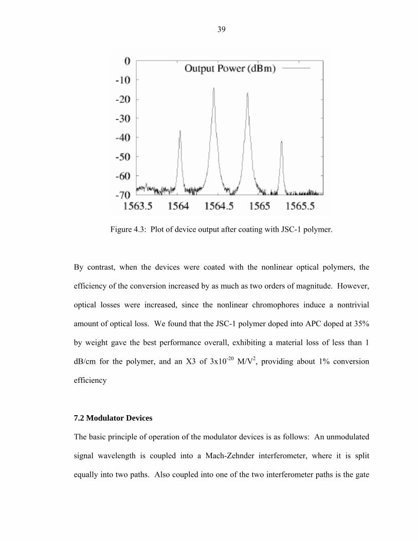
Figure 4.3: Plot of device output after coating with JSC-1 polymer.
By contrast, when the devices were coated with the nonlinear optical polymers, the
efficiency of the conversion increased by as much as two orders of magnitude. However,
optical losses were increased, since the nonlinear chromophores induce a nontrivial
amount of optical loss. We found that the JSC-1 polymer doped into APC doped at 35%
by weight gave the best performance overall, exhibiting a material loss of less than 1
dB/cm for the polymer, and an X3 of 3x10-20 M/V2, providing about 1% conversion
efficiency
7.2 Modulator Devices
The basic principle of operation of the modulator devices is as follows: An unmodulated
signal wavelength is coupled into a Mach-Zehnder interferometer, where it is split
equally into two paths. Also coupled into one of the two interferometer paths is the gate

40
signal, which is a modulated optical signal. This modulated optical signal causes a
change in the index of refraction of the arm to which it is coupled. This results in a phase
delay for the half of the signal wavelength that is traveling through that arm, and thus a
change in the output power of the device after the final coupler, which recombines the
two halves of the signal. Having changed the relative phase of one of the arms, the
transmitted power is altered by the presence of the gate signal.
Figure 4.4: Graphic of modulator device layout
There are several details of the device design that merit discussion. For the combination
of the gate and source wavelengths, it was necessary to design components that could be

41
used to combine different wavelengths on the arms of the interferometer. Although it is
possible to produce muxes that will couple two different wavelengths into the same
waveguide with relatively low loss, we found that such devices were fairly unrepeatable
in our processes. Instead of a mux, we elected to use 3 dB directional couplers on both
arms, which are highly repeatable and broadband, though of course they incur a
substantial optical loss. In order to make the Mach-Zehnder approximately balanced,
these couplers had to be placed on both arms, even though only one is actually used for
the experiment. Lastly, the Mach-Zehnder is designed to be intrinsically unbalanced,
with one arm having a length of 1.2 cm, and the other a length of 1.24 cm.
Figure 4.5: Graphic of the die layout and enlargement of the input region of the
interferometer.

42
Device Fabrication
Our devices were fabricated in 120 nm thick silicon-on-insulator layers by using electron
beam lithography at 100 kV with a Leica EBPG 5000+ beamwriter. Beam step sizes
were set to 5 nm, allowing the use of a 360 micron field.
Figure 4.6: Optical image of the input and output portion of a typical device, with
illustrations showing the flow of optical power.
A direct-written hydrogen silsesquioxane hardmask was used to define the waveguides,
and the devices were etched with a chlorine-based recipe in an Oxford PlasmaLab 100
inductively coupled plasma reactive ion etcher. A number of different polymers were
coated, in order to determine which chromophore loading would exhibit the best
nonlinear behavior. The samples were then briefly dipped in buffered HF, in order to
remove the resist from the surface and in order to provide a slight undercut, improving
the modal overlap with the cladding.

43
The devices discussed herein were coated with AJLS102/APC polymer at 30%
chromophore loading and 14 weight percent concentration, with a solvent of
cyclohexanone. The spin rate was 1800 rpm for approximately 1 minute. The samples
were then baked in a vacuum oven overnight in order to remove any residual solvent.
This third-order nonlinear polymer proved to be robust over several days of testing, and
formed clean films over centimetre scale areas.
7.3 Experimental Results
Testing of these devices was performed using our planar, wafer-scale optical test setup.
This setup allows for relatively low-loss single-mode coupling into the devices; losses are
typically on the order of 5 dB, with an uncertainty of around 1 dB. More importantly,
this setup allows for the automated measurement of very large numbers of devices. To
begin with, the devices were tested passively, with low optical power, in order to
characterize their linear response.
Figure 4.7: Graphic showing Mach-Zehnder transmission spectrum as a function of
wavelength.

44
Terahertz experiments
Generating terahertz-scale test signals electrically is not a straightforward proposition,
and there are no modulators available that could be used to add such an amplitude
modulation to a continuous-wave laser signal. Nevertheless, in order to characterize
these devices at speeds in the terahertz, we needed a terahertz test tone. In order to
generate such a signal, we took advantage of the Vernier effect; by linearly
superimposing two closely spaced coherent optical signals, we were able to produce a
slowly varying envelope function at the difference frequency. For example, two laser
signals copropagating in the same waveguide with wavelengths near 1550 nm whose
wavelengths are spaced apart by .8 nanometers will provide an intensity modulation in
the waveguide at a frequency of about 100 GHz. Given the fact that our input optical
couplers are broadband, accepting signals over about 20 nm of bandwidth, this turned out
to be a feasible way to generate very high frequency test signals.
Figure 4.8: Layout of THz Experiment
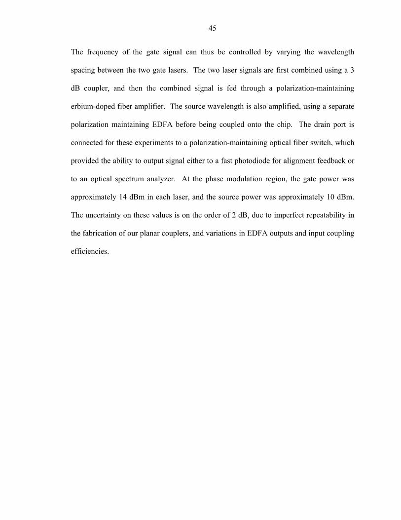
45
The frequency of the gate signal can thus be controlled by varying the wavelength
spacing between the two gate lasers. The two laser signals are first combined using a 3
dB coupler, and then the combined signal is fed through a polarization-maintaining
erbium-doped fiber amplifier. The source wavelength is also amplified, using a separate
polarization maintaining EDFA before being coupled onto the chip. The drain port is
connected for these experiments to a polarization-maintaining optical fiber switch, which
provided the ability to output signal either to a fast photodiode for alignment feedback or
to an optical spectrum analyzer. At the phase modulation region, the gate power was
approximately 14 dBm in each laser, and the source power was approximately 10 dBm.
The uncertainty on these values is on the order of 2 dB, due to imperfect repeatability in
the fabrication of our planar couplers, and variations in EDFA outputs and input coupling
efficiencies.
46
Figure 4.9: Panels at top, left, and right show modulation of the source laser at 2.6 THz,
0.6 THz, and 0.25 THz, respectively. In the right panel, it is important to note how the
signal transmission changes with wavelength, while the modulation sideband does not
change in magnitude; this is the unmistakable signature of an amplitude modulator.
Measurements at higher frequencies are difficult due to bandwidth limitations of our test
equipment and of our optical couplers, but we predict that a device like ours will function

47
at rates of 10 THz – the fundamental limitation on such devices is dispersion in the
waveguides.
As a travelling-wave device, the only limitation of the response speed of the device is the
dispersion of the waveguide causing phase matching conditions to be violated at very
high speeds. Through careful dispersion engineering of waveguides, this could be very
likely be improved upon. It is of note that there are a number of peaks exhibited that are
neither modulation sidebands nor input laser frequencies. These are the result of the
source wavelength phase-modulating the gate frequencies.
One key feature of the data shown in the figure 4.9 is that as the source wavelength is
tuned across the interferometer peaks, the drain signal at the same wavelength changes
substantially in intensity. However, the modulated sidebands do not change their
intensity. This is the unmistakable signature of an intensity modulator, as opposed to a
phase modulator. In comparing a phase modulator to an intensity modulator, it is
important to note that in both cases, the nonlinear region appears in one or both of the
arms of the device. The output amplitude of a phase modulator in a waveguide of length
L can be written as
))()/(cos()( tcLtwAtE φΔ+−=
On the other hand, an unbalanced Mach-Zehnder with phase modulation on a single arm
can be written as:
)))()/1(cos())/0((cos(2
)( tcLtwcLtwAtE φΔ+−+−=
48
In the time domain, the difference between these two devices would be easily
visible. However, for our highest speed measurements, equipment to perform this
measurement was not available, and we only had frequency domain information.
Fortunately, as can be seen from these two equations, and as we have shown in our
measurements, a Mach-Zehnder modulator can be distinguished from a pure phase
modulator by tuning the signal wavelength and observing the extinction of the central
peak, independent of the amplitudes of the side bands.
It is possible to relate the phase shift occurring in the modulator to the extinction
ratio between the central peak and the sideband. Taking f as this ratio, the relationship is,
to a very good approximation:
f4=Δφ
For the modulator shown in figure 4.9, typical values of f were -40 dB, indicating
an approximate phase shift of .04 radians with 14 dBm of gate power, implying a
relatively small extinction for this modulator device. However, by trading increased
insertion loss for increased modulation ratio (by changing the point of operation of the
unbalanced Mach-Zehnder interferometer), it would be possible to achieve an extinction
of 3 dB with -24 dB of intrinsic insertion loss in our device. However, because of the
limitations of our test setup, we were only able to operate in the low-loss/low-extinction
regime. An effective nonlinear χ3 coefficient can be estimated as 1x10-20 (m/V)2, and the
nonlinear coefficient of the polymer is approximately three times that value. Typical
results for Δφ ranged from .02 to .04 radians during testing for this gate power level.

49
Figure 4.10: Test data showing movement of sidebands with change in modulation
frequency from .5 nm to 20nm spacing. The rolloff at high frequency is largely
accounted for by the reduction in coupler efficiency off-peak
Gigahertz Experiments
One of the features of the all-optical data is that the optical spectrum analyzer does not
give any phase information – only amplitude. So although we could indirectly see that
we had an intensity modulator, from our ability to change the bias point of the
unbalanced MZI without changing the magnitude of the modulation sidebands, there was
no direct confirmation that what was being generated was pure amplitude modulation. In
point of fact, the peaks generated by our devices are at exactly the same wavelengths as
the peaks that would be generated by a pure phase modulator based on the same effects.

50
In order to confirm our interpretation of the all-optical results, we performed a second
experiment, making use of more-conventional microwave measurement technology.
In general, passive microwave components are characterized by frequency-dependent S-
parameters. These parameters specify the phase and amplitude coupling between an
input and an output port of a given device at a given frequency. The tool used to measure
such S-parameters is called a Vector Network Analyzer (VNA). Such a system works by
sending an RF test tone of known amplitude and phase into one port of a device, and
measuring the amplitude and phase of the returned signal. By sweeping the frequency of
the test tone, it’s possible to characterize the spectrum of S-parameters across a very wide
bandwidth.
In our experiment, of course, our signals are not purely microwave. They are, at least
within the device, modulated onto an optical carrier, whose frequency is in excess of 100
THz. Fortunately, there exists a system designed to do radio frequency measurements of
optical components, originally developed for testing telecommunication components.
The particular system we used is an Agilent 8703B, which is a VNA that has both optical
output and input. The optical output is a continuous-wave diode laser which is then fed
through an integrated electrooptic modulator. The optical input is a calibrated
photodiode with bandwidth in excess of 20 GHz.

51
Figure 4.11: Layout of the gigahertz modulation experiment
In this experiment, the source wavelength was a single continuous-wave laser boosted in
power by an EDFA. For the gate wavelength, we used a second laser, which was
modulated by the optical modulator built into the 8703 and then boosted in power by a
separate EDFA.
It is important to note that both the source and gate wavelengths are coupled out of the
chip at the drain. For the all-optical terahertz measurements described previously, In
order to distinguish between the various laser wavelengths used in the experiment, we
had to use an wavelength filter downstream from the modulator devices. Output was
coupled either through this filter and into the detector port of the 8703, or directly from
the drain to the OSA.

52
The conditions of the experiment were controlled so that at the input to the phase
modulation region the source power was 10 dBm, and the gate power was 17 dBm.
Control experiments were performed with a simple PMMA cladding; having observed
that there was no modulation detected at the output on the source wavelength, data was
then taken for devices with the nonlinear optical cladding.
Figure 4.12 shows the optical S-parameter measured with the 8703B. This data shows a
large modulation below approximately 3 GHz, which we attribute to slow effects such as
free-carrier excitation. At higher frequency, the coupling with both the source and gate
lasers turned on is clearly several dB in excess of the noise level of the instrument. The
background noise level in the instrument is, in fact, quite similar to the measured data
when either the source or gate laser is turned on by itself, as shown in the plot.
In addition, this same measurement was performed, but the output was routed to the OSA
instead of the VNA. This allowed the observation of the sidebands on the input signal
and those on the output of the device. The modulation of the source wavelength at the
output of the device is clearly visible in the sidelobes shown in figure 4.13.
It is of note that, because the detector used in the VNA experiment is a photodiode, it will
not measure pure optical phase modulation; the bandwidth of the detector being in the
gigahertz excludes that possibility. Thus, this experiment shows unambiguously that the
modulation we are observing is in fact amplitude modulation.

53
Furthermore, the black horizontal line superimposed on Figure 4.12 shows the calculated
S-parameter extracted from the previously shown terahertz dual-laser gate experiment.
This value is found to be in very close agreement with the S parameter measured in the
Gigahertz, indicating that this modulator has approximately the same performance from 5
GHz to 2.5 THz.
Figure 4.12: Shows the measured S-parameter for the device in various circumstances.
The red curve is the measured value of the S-parameter when both the gate and source
lasers are on. For control, we show the same measurement taken when the signal laser is
off, when the pump is off, and when all lasers are off, shown with the green, blue, and
teal curves, respectively. The predicted S-parameter of -37 dB from the dual gate
experiment is also shown as a black line, and is found to be in close agreement with the
S-parameter measured.

54
Figure 4.13: Optical spectrum traces taken for various sinusoidal radio-frequency
intensity modulations on the gate. The intensity modulation of the gate laser results in
sidebands output, located near the source wavelength at the appropriate locations for each
input modulation frequency. The panel at right shows a detail of the device output near
the source wavelength for modulation at 10 GHz, 15 GHz, and 20 GHz.
1 A. F. J. Levi. “Optical Interconnects in Systems.” Proceedings of the IEEE 88 (6), 750-757 (2000). 2T. Brabec, F. Krausz. “Intense few-cycle laser fields: Frontiers of Nonlinear Optics.” Rev. Mod. Phys. 72, 545–591 (2000). 3 W. Hafez, W. Snodgrass, M. Feng. “12.5 nm base pseudomorphic heterojunction bipolar transistors achieving fT=710 GHz and fMAX=340 GHz.” Appl. Phys. Lett. 87, 252109 (2005) 4 R. Boyd. “Nonlinear Optics.” New York: Academic Press, 2003. 5 Appl. Phys. Lett. 87, 252109 (2005) (3 pages) 6 W. Hafez, W. Snodgrass, M. Feng. “12.5 nm base pseudomorphic heterojunction bipolar transistors achieving fT=710 GHz and fMAX=340 GHz.” Appl. Phys. Lett. 87, 252109 (2005) (3 pages) 7 www.keopsys.com 8 A. Yariv. “Optical Electronics in Modern Communications.” New York: Oxford University Press, 1997.

55
9 S. Arahira, Y. Ogawa. “High-repitition-rate optical pulse generation and control techniques.” Measurement Science and Technology 13, 1664-1670 (2002). 10 M. Dinu, F. Quochi, and H. Garcia, “Third-order nonlinearities in silicon at telecom wavelengths.” 82 (18), 2954 (2003). 11 Arivuoli, D., Fundamentals of nonlinear optical materials. Pramana – J. Phys. 57, 871-883 (2001). 12 Ö. Boyraz, P. Koonath, V. Raghunathan, and B. Jalali, "All optical switching and continuum generation in silicon waveguides," Opt. Express 12, 4094-4102 (2004)
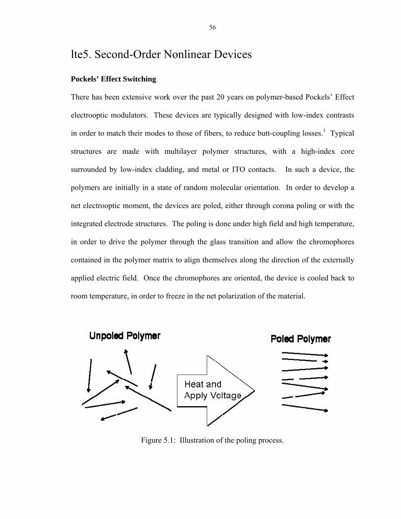
56
lte5. Second-Order Nonlinear Devices
Pockels’ Effect Switching
There has been extensive work over the past 20 years on polymer-based Pockels’ Effect
electrooptic modulators. These devices are typically designed with low-index contrasts
in order to match their modes to those of fibers, to reduce butt-coupling losses.1 Typical
structures are made with multilayer polymer structures, with a high-index core
surrounded by low-index cladding, and metal or ITO contacts. In such a device, the
polymers are initially in a state of random molecular orientation. In order to develop a
net electrooptic moment, the devices are poled, either through corona poling or with the
integrated electrode structures. The poling is done under high field and high temperature,
in order to drive the polymer through the glass transition and allow the chromophores
contained in the polymer matrix to align themselves along the direction of the externally
applied electric field. Once the chromophores are oriented, the device is cooled back to
room temperature, in order to freeze in the net polarization of the material.
Figure 5.1: Illustration of the poling process.
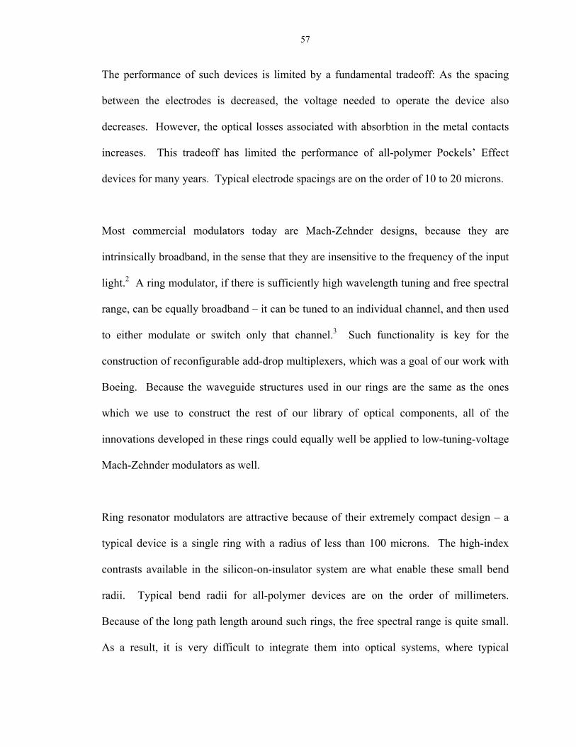
57
The performance of such devices is limited by a fundamental tradeoff: As the spacing
between the electrodes is decreased, the voltage needed to operate the device also
decreases. However, the optical losses associated with absorbtion in the metal contacts
increases. This tradeoff has limited the performance of all-polymer Pockels’ Effect
devices for many years. Typical electrode spacings are on the order of 10 to 20 microns.
Most commercial modulators today are Mach-Zehnder designs, because they are
intrinsically broadband, in the sense that they are insensitive to the frequency of the input
light.2 A ring modulator, if there is sufficiently high wavelength tuning and free spectral
range, can be equally broadband – it can be tuned to an individual channel, and then used
to either modulate or switch only that channel.3 Such functionality is key for the
construction of reconfigurable add-drop multiplexers, which was a goal of our work with
Boeing. Because the waveguide structures used in our rings are the same as the ones
which we use to construct the rest of our library of optical components, all of the
innovations developed in these rings could equally well be applied to low-tuning-voltage
Mach-Zehnder modulators as well.
Ring resonator modulators are attractive because of their extremely compact design – a
typical device is a single ring with a radius of less than 100 microns. The high-index
contrasts available in the silicon-on-insulator system are what enable these small bend
radii. Typical bend radii for all-polymer devices are on the order of millimeters.
Because of the long path length around such rings, the free spectral range is quite small.
As a result, it is very difficult to integrate them into optical systems, where typical

58
adjacent channel spacings are on the order of 100 GHz. SOI resonators like ours have
been demonstrated with radii down to a few microns, and correspondingly large free
spectral ranges. Although we worked chose to work with larger rings because it eases the
tolerances for overlaying top layers, it is obvious that our work could be extended to
substantially smaller ring diameters and larger free spectral ranges.
In our work on novel Pockels’ Effect optical modulators, we have developed two
approaches for breaking this tradeoff. The first, which was pursued in collaboration with
our collaborators at Boeing Phantom Works, was to use conventional silicon waveguides
in order to concentrate the optical fields, allowing electrode structures to be moved closer
to the optical waveguides without incurring devastating loss penalties. The second is to
use a slotted waveguide4 and dope it until it is electrically conductive. This approach has
the advantage of reducing the electrode gap to the order of 100 nm, without incurring
substantial excess optical losses. Experiments were performed that show proof-of-
concept for both of these approaches.
Basic Temperature and Index Tuning Experiments
In order to validate our theoretical understanding of the ring resonator system,
experiments were performed where effective index of the waveguide was tuned
thermally. This work is also of some technological relevance, since being able to predict
the behavior of ring devices under conditions of wide temperature change is a necessary
prerequisite to their application in commercial devices. A semianalytic approach to
calculating the resultant tuning in effective index for a change in the index of some

59
specific area of a waveguide was developed. This approach takes advantage of the ability
to use a Hermetian Eigensolver to predict accurately the shapes of the optical modes, and
relies upon a perturbation theory approach developed originally by T. Baehr-Jones.5 This
semianalytic methodology could be used to calculate the influence of changes in either
the cladding or the core of the waveguide.
Figure 5.2: Modal profile of the Silicon waveguide and the dispersion plot of a pmma
clad waveguide. The profile is of |E|, with contour lines drawn in increments of 10%
starting at 10% of the maximum field value. The panel at right shows effective index as a
function of wavelength.
It is well known that for a ring resonator, the spectral location of a resonance is governed
by the following relationship, where L is an effective path length around the ring
resonator, m is an integer, λ is the wavelength of the resonant frequency in free space,
and neff(λ) is the effective index of the waveguide:

60
)(λλ
effnmL=
However, when neff can change with temperature and wavelength, we have:
λλ
εε
dn
dTT
ndn effc
c
effeff ⎟⎟
⎠
⎞⎜⎜⎝
⎛∂
∂+⎟
⎠⎞
⎜⎝⎛∂∂
⎟⎟⎠
⎞⎜⎜⎝
⎛∂
∂=
Here εc is taken to be the dielectric constant of the material that is being temperature
tuned – in this case the core of the silicon waveguide.
So the expression for the location of a resonance is found to be:
)(
)(21
0
0
1
λ
ελλ
eff
sisi
c
effeff
nmL
TTTnn
nnmL
mL
+
−⎟⎠⎞
⎜⎝⎛∂∂
⎟⎟⎠
⎞⎜⎜⎝
⎛∂
∂⎟⎟⎠
⎞⎜⎜⎝
⎛⎟⎟⎠
⎞⎜⎜⎝
⎛∂
∂⎟⎠⎞
⎜⎝⎛−=
−
Here we take T0 to be the lowest temperature that the ring was measured at, which was
in our case 20˚C; then, λ0, m and neff(λ0) are the resonance peak under study observed at
this temperature. This expression suggests that when plotted as a function of temperature,
the position of a given resonance peak should be linear. The slope is dependant on the
product of well-known physical constants and the results of our modesolver and
perturbation theory; in particular, the temperature derivative of the index of refraction of
silicon is known to be 1.5x10⁻⁴ 1/K at room temperature.6 We did not use a cladding on
the ring resonators for the temperature tuning; that is, above the waveguide there was
simply air, and below the waveguide, silica. Since the silica has a temperature derivative
of the index one order of magnitude less7 than silicon, it is ignored for the purposes of the

61
above expression.
The dependence of the location of the resonance peaks on temperature and cladding
index was measured in order to verify our predictions. As the temperature of the stage
holding a chip was varied, the temperature at the surface of the stage was monitored, and
an optical resonator peak was traced. A series of measurements were made at different
temperatures, allowing curves of wavelength versus temperature to be constructed. We
estimate the uncertainty of our temperature control to be about .1˚ C. A typical set of
transmission spectra that were observed can be seen in figure 5.3. All of the spectra that
we show are normalized to remove the unimportant insertion loss spectrum of our
measurement setup.

62
Figure 5.3: Normalized fiber to fiber transmission in dB as a function of wavelength in
nm for two different temperatures for one of the ring resonators studied. The transmission
has been normalized against our baseline fiber to fiber coupling efficiency. A detailed
plot of the peaks near 1498 nm is shown.
We repeated such measurements several times for each temperature value on one
device, to allow the estimation of the characteristic measurement uncertainty that our
system had. We measured the temperature dependence of a second ring resonator as well,
but taking only one data point for each temperature. Both devices consisted of 30-micron-

63
bend-radius ring resonators. The ring-to-input waveguide spacing was 0.37 micron, edge
to edge. The Q in this case was approximately 20,000, and these rings were air clad.
During our experiments, meaningful changes in the Q’s and the extinctions of the
resonance peaks were not observed to the limits of our testing apparatus.
Figure 5.4: Panel at left shows dn/dλ versus wavelength in 1/nm, while the right panel
lists the simulated susceptibility to core changes, a dimensionless quantity as a function
of wavelength. In the bottom panel, we show the movement of a resonance peak as a
function of temperature offset, in degrees Celsius. The base temperature was 20˚C. Also
shown is the predicted behavior.

64
The small discrepancy between the predicted behavior and the results is likely
attributable to either slight error in the solved mode profile, or to a slightly incorrect
value for the index of silicon at room temperature; 3.46 was used in the simulations.
Most importantly, however, the experimental results are quite close to the theoretical
ones, and this close match verifies that there are no major factors being left out of our
model for these resonator systems.
Polymer-Clad Waveguide Devices
The first class of devices developed, in collaboration with Boeing Phantom Works,
comprised simple silicon waveguides, clad in active polymer. The modulation effect in
these devices is due to the interaction of the optical field with the active polymer
cladding. Electrodes are integrated either laterally or vertically on top of our waveguide
devices at Boeing, using standard photolithography and metal deposition.

65
Figure 5.5: Micrograph of planar electrodes surrounding silicon waveguides, courtesy of
Boeing Phantom Works.
This design allowed the electrodes to be brought within a couple of microns of the
waveguiding region. The test devices were designed as 1x4x1 ROADMs; these have one
input and output on a bus waveguide, and four rings, each of which can be tuned to any
of four different optical channels. The goal of this work was to show the ability to tune
each ring within a device across four full widths at half maximum, as this is a minimum
channel separation for reasonable data transmission specified by our DARPA funding
program. The Q’s of the devices were spoiled to values on the order of a few thousand
by making the spacing of the directional couplers small. Typical directional coupler
spacing for these devices was on the order of 200 nm.

66
Figure 5.6: GDS file layout of 1x4x1 ROADM devices.
x64.100 Device 4 DC modulation
-60
-55
-50
-45
-40
-35
-30
-25
1525 1526 1527 1528 1529 1530 1531 1532 1533 1534 1535
wavelength
pow
er
Step 1: 0V
Step 2: +300V
Step 3: 0V
Step 4: -300V
Figure 5.7: Data from a device measured at Boeing Phantom Works showing in excess
of three full-width at half max tuning.
Typical results show more than three FWHM of tuning with a total swing of 600 Volts.
These devices were coated with 25% YL124 in APC, and were prepared with metallized
chrome-gold contacts using standard photolithographic and metal deposition techniques.
67
The electrodes in this case were in-plane, and were spaced 5.25 microns apart, and the
device was poled at 60V/micron at 137 degrees C.
Pockels’ Effect Slotted Waveguide Devices
A more aggressive technological approach to making tunable ring resonators is to use the
slotted waveguides originally developed by Lipson et al.8 By using the silicon as both
the optical waveguide and as the electrical contact, the tradeoff between operating
voltage and optical loss implied by varying the metal gap spacing around an optical
guiding waveguide core can be eliminated. These slot waveguides allow for a very high
concentration of optical field in the central gap formed by the two optically guiding
“rails.” Such a geometry results in electric field strengths on the scale of 106 V/m for
optical input power levels on the milliwatt scale. Such a geometry provides intrinsic
electrical isolation between the two silicon strips, which are fully etched to the oxide etch
stop, allowing relatively large electrical fields to be dropped across the central gap.
Taking advantage of the tiny scale of this gap, we demonstrate low-voltage Pockels’
Effect tuning of slot ring resonators. We have demonstrated the fabrication of slot
waveguides and resonators with losses on the order of -10dB/cm.

68
Figure 5.8: Mode shape for an electrooptic-polymer-clad slot waveguide showing 10%
contours for electric field.
Figure 5.9: Device layout for testing shows electrodes, resonator, and optical couplers.
It was necessary to establish independent electrical contact to both the inner and outer
rings, in order to hold them at separate voltages. This must be done without inducing
substantial excess optical losses, which would ruin the Q’s of the resonators. This
electrical contact was accomplished with a segmented waveguide structure, shown in the

69
figure 5.10 at three different magnifications. This structure has been simulated to exhibit
approximately .1 dB of optical loss, and provides electrical contact to both the inner and
outer rings.
Figure 5.10: Images at various magnifications of the electrical contact structures used to
establish independent electrical contact to the inner and outer portions of the slot ring
resonators.
Device Fabrication
These slot waveguide resonator devices were fabricated in silicon-on-insulator with a top
layer thickness of 110 nm, and an oxide of 1.3 microns. The samples were cleaned and
rinsed in solvents, and then baked for 20 minutes at 180C in order to remove residual

70
water from the surface. They were then spun at 1000 rpm and coated with 2% HSQ resist
obtained from Dow Corning Corp. In order to remove the solvents in the resist
suspension, samples were baked for 20 minutes at 180C once again.
Structures were lithographically defined using the Leica EBPG 5000+ vector-scanned
electron beam system. The structures were exposed at 100 kV, 5 nm step size, and 3500
µC/cm2 dose. Development was performed in AZ 300 TMAH metal-ion-free developer
for a time of 3 minutes at room temperature. The samples were then etched in an Oxford
Plasmalab ICP RIE under the following conditions: Chlorine at 80 sccm, forward power
at 50 W, ICP power at 800 W, 12 mTorr pressure, and 33 seconds of etch time. At this
point some samples were tested for passive optical performance. The wafers were then
implanted with phosphorous at normal incidence, 30keV energy, and 1x10¹⁴ ions/cm2
density and annealed at 950C in a vacuum rapid thermal anneal system, yielding a
resistivity of about .025 Ohm-cm. Finally, the samples were briefly dipped in buffered
hydrofluoric acid, which both removed resist remnants and provided a slight undercut,
increasing the mode overlap with the electrooptic cladding materials.

71
Figure 5.11: SEM image at grazing incidence of and slot resonator. Note the slight
undercut, and the clean top surface after the buffered hydrofluoric acid dip. The central
gap in this case is approximately 70 nm wide.
After passive optical testing with polymethylmethacrylate claddings, the devices were
generally coated with either YLD 124 electrooptic polymer or with dendrimer-based
electrooptic materials. When not in use, the samples were stored under a vacuum in
order to prevent oxidation of the organic materials.
Confirmation of Gap Filling
One important result that bears mention regards the filling of the slots with polymer.
Because we did not observe substantial excess optical losses, it was clear that there was
not major bubble formation occurring in the waveguide gaps. However, we wanted to
obtain direct evidence that the gaps were being completely filled with our organic

72
materials. A study was performed using a dualbeam scanning electron
microscope/focused ion beam system, where we were able to cut through the polymer
and silicon layers, and obtain cross sectional images, such as the one shown below. This
study confirmed that the gaps were indeed being filled with the organic polymer
materials.
Figure 5.12: SEM images of FIB cross section show that gap is fully filled with
polymers, without void formation
Failure Mechanism
It was found that the devices are generally very robust up to approximately 30 Volts,
though above that level they have a tendency to fail electrically. The electrical failure
mechanism is surmised to be through the formation of a short electrical path through the
polymer coating.

73
Figure 5.13: Scanning electron micrographs of devices that failed electrically, after
polymer decoating in solvent.
Results – Split Ring
Pockels’ Effect devices were characterized both for DC and for AC performance.
Because these devices were not designed to reduce parasitic resistance and capacitance, it
is unsurprising that the AC performance falls off quickly with frequency. The DC
characterizations were performed by biasing the devices to a series of different voltages
and taking wavelength-scanned transmission measurements. In general, an additional test
was performed where the order of the voltages was randomized, in order to eliminate any
systemic drift from the measurements.

74
Figure 5.14: Typical results for split-ring resonator tuning. In this case the polymer
system was YL/APC, and the poling conditions were 120C, 20V (outer ring positive), 12
minutes, voltage off after cooling to 30C.
For AC measurements, a square wave input voltage was used, and the input wavelength
was tuned until the output signal exhibited maximum extinction. This point is of course
where the resonance peak exhibits the highest slope, and is thus quite sensitive to small
drifts in the system. Although in a future realization of these devices this could be done
inside of a slow thermal feedback loop in order to stabilize the behavior of the system,
such a feedback system was not implemented in these measurements. Immediately
following the measurement of AC data, a wavelength sweep was performed in order to fit
the observed optical output power swing to the tuning excursion of the resonators. AC
tuning was measured into the low megahertz, and the falloff in device response at high
frequencies was attributable to the parasitic resistance and capacitance of the system,
rather than to any falloff in the response of the electrooptic material itself.
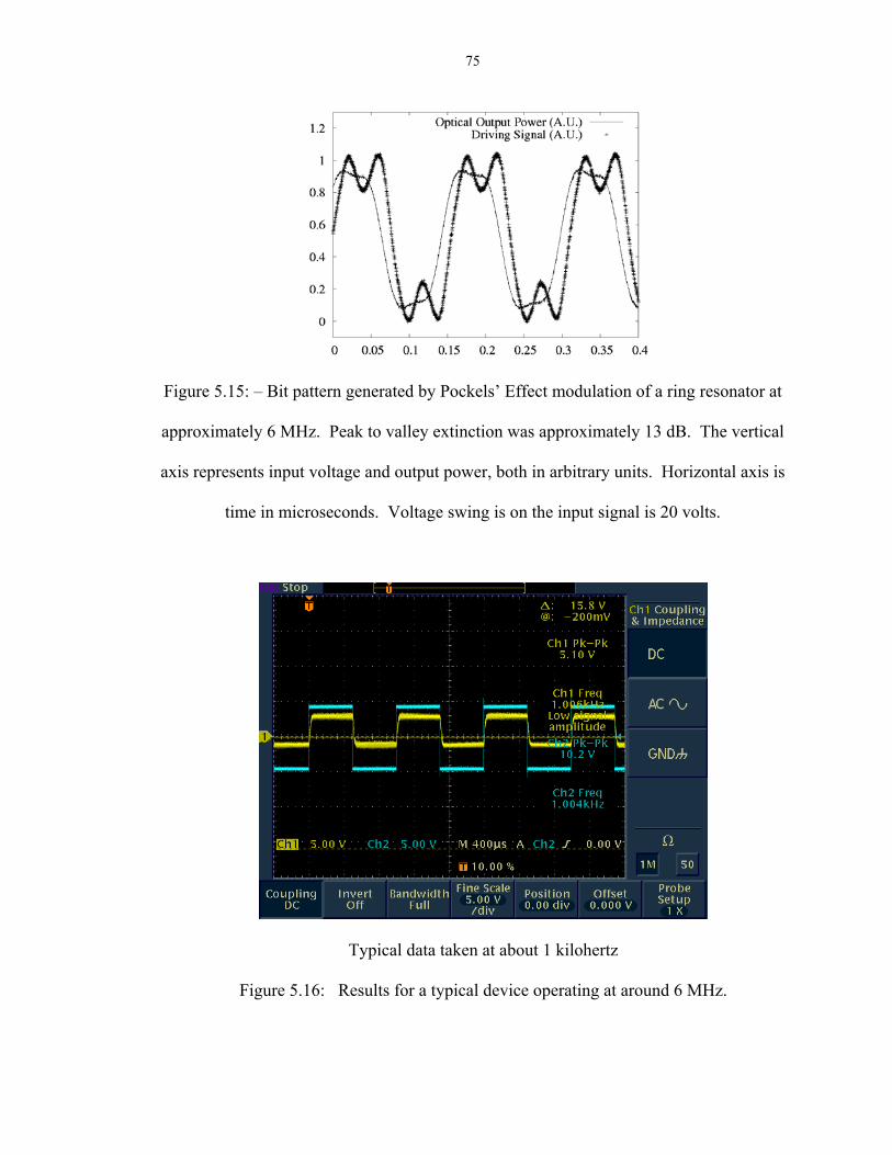
75
Figure 5.15: – Bit pattern generated by Pockels’ Effect modulation of a ring resonator at
approximately 6 MHz. Peak to valley extinction was approximately 13 dB. The vertical
axis represents input voltage and output power, both in arbitrary units. Horizontal axis is
time in microseconds. Voltage swing is on the input signal is 20 volts.
Typical data taken at about 1 kilohertz
Figure 5.16: Results for a typical device operating at around 6 MHz.

76
These devices are not optimized as modulators, but were instead a proof-of-concept
for this type of slot waveguide device. By increasing the Q of the resonators to exceed
20,000, which has been demonstrated elsewhere,9 it will be possible to achieve much
larger extinction values per applied voltage. We anticipate being able to produce
compact modulators based upon single rings with high extinction even with voltage
swings significantly below 1 Volt. In addition, such devices can be greatly enhanced by,
for instance, using multi-ring Vernier tuning structures.
Finally, by using more-advanced dendrimer-based electrooptic materials, we were able
to substantially improve the tuning figures to .042±.008 nm/V, or 5.2±1 GHz/V for these
rings, which translates to an r33 value of 79±15 pm/V. This result is better than those
obtained1011 for rings of 750 micron radius, which we believe to be the best tuning figure
published to date. By contrast, our rings have radii of 40 microns. We credit our
improvement over the previous results mainly to the field enhancement properties of our
waveguide geometry. Our devices are substantially smaller than the state of the art all-
polymer devices due to intrinsic advantages in the high-Q slot ring based approach.
Optical Rectification
Although the above data represents a radical departure in the size and performance of
Pockels’ Effect devices, it by no means represents a fundamental innovation. They use a
very well-known effect – to wit, by applying an electric field to an optical material with a
second-order nonlinear moment the index of refraction can be changed. The Pockels’
Effect modulators do not take any particular advantage of the high mode-field

77
concentrations available in the silicon-on-insulator system; the response of these devices
is essentially insensitive to the optical power circulating in the device. In addition to the
Pockels’ Effect, we were able to observe a truly ultrafast nonlinear optical effect in these
devices – optical rectification.12
Optical rectification is an effect that is based on an optical wave mixing with itself down
to DC. This mechanism permits the creation of optical detectors that operate without bias
voltage, and where the mechanism of the optical-to-electrical conversion is not limited by
free-carrier diffusion times. We demonstrate direct conversion of optical energy to
electrical energy with continuous-wave power levels of less than 1 milliwatt; this is six
orders of magnitude lower than the next best device reported to date to our knowledge,
which required instantaneous fluences of over a kilowatt.13
The devices for these experiments were identical to the Pockels’ Effect slot-ring
modulators described previously, which consist of electrically contacted, doped ring
resonators. Once again, the slotted waveguides serve as both transparent electrical
contacts and as optical waveguides. These devices take advantage of the massive mode-
field concentration provided by the slot rings; peak electric fields for continuous-wave
pumping on the scale of 1 mW into a slot waveguide result in a peak electric field on the
scale of 106 V/m. Because the two strips forming the waveguide are fully etched down to
the bottom oxide, there is excellent electrical isolation between the two sides of the
waveguide. This slot etch is extremely similar to the shallow trench isolation etches
common in SOI front-end electronics fabrication processes. The close proximity of the

78
electrical contacts to this high optical field make these slot waveguides a unique system
for the study of optical rectification.
Experimental Results
Testing of these devices as optical detectors proceeded similarly to the testing of the
Pockels’ Effect modulators. Contact was established to the pads by scratching through
the polymer or dendrimer layers, and confirmed through measuring leakage currents or
direct-current modulation. Optical energy was coupled into the devices thorough
polarization maintining single-mode fiber arrays, taking advantage of our out-of-plane
optical test setup. The samples were held at controlled temperature with a digitally
controlled heating stage. Optical alignment was maintained using a computer-controlled
optical feedback stage system.
A shunt resistor on the right-hand pads, as shown in Figure 5.16, provides a means of
confirming electrical contact, and typical pad-to-pad and pad-to-ring resistances range
from 1 MΩ to 5 MΩ. Figure 5.17 below displays the equivalent circuit diagram for a
device when it is functioning as a detector; where a current is spontaneously induced by
the optical signal and is measured between the two electrical pads. Two pads are
connected to the center of the ring, and two to the outside portion.

79
Figure 5.17: Equivalent circuit of an optical rectification device
For the rectification experiments, the input optical signal was magnified with a Keopsys
polarization-maintaining erbium-doped fiber amplifier. When the laser and EDFA were
powered on, a DC current was observed between pads connected to the outer and inner
rings. This current was measured with a Keithley pico-ammeter. In our best devices, a
DC current of about 1.3 nano-Amps was observed; this corresponded to an electrical
output of about 5x10-12 W. This corresponded to a wall-plug efficiency of about 10-9,
which is by no means spectacular. Control devices, which were coated with either
polymers not containing chromophores or unpoled electrooptic polymers, showed no
electrical current. When the optical power was turned off, the electrical output of these
devices disappeared. It is worthy of note that the amount of optical energy being
converted to electricity is dramatically less than the amount being coupled through the
device to the output port or lost through scattering, which suggests that with further

80
engineering, significant improvements can be made to the efficiency of devices like those
discussed here.
In addition to cycling the power on the input optical channel, several other experiments
were performed in order to ‘sanity check’ the results. Devices were tested prior to poling
and then after poling, and devices were uncoated and recoated with inactive polymers.
Electro-optic polymer coated devices were thermally cycled in order to remove the
second order optical moment induced by poling. The optical signal was removed by
moving the stage, without changing anything electrical or optical. In all of these tests, the
expected results were obtained.
One important confirmation that what we were observing was indeed optical rectification
was based on the direction of the current generated by the devices. This direction is
determined by the direction in which the device was poled. Devices could, of course, be
poled with the inner ring high or low voltage – these two conditions result in an inversion
of the electrooptic moment of the materials filling the slow waveguides. Furthermore,
putting a steady bias on the chip for several minutes, as shown in TABLE CCC results in
a substantial change in the photoresponse of the device, and this change depends on the
polarity of the bias voltage, after that bias has been removed. Because of the very large
fields that can be induced in the gaps with even quite low voltages applied, we believe
that these DC bias voltages are causing the chromophores in the slots to reorient
themselves even at room temperatures.
Table 5.17. Polling Results

81
Part A: Action New Steady State Current (6 dBm input) Initial State -5.7 pA +10V for 2 minutes 0 pA -10V for 2 minutes -7.1 pA +10V for 2 minutes -4.4 pA +10V for 4 minutes -6.1 pA +10 V for 4 minutes -4.5 pA -10 V for 2 minutes -14.8 pA Part B:
Device Action Current Polarity of Optical
Rectification 1 Positive Poling Positive 1 Thermal Cycling to
poling temperature with no voltage
Rapid fluctuation, did not settle
1 Negative Poling Negative 2 Negative Poling Negative 2 Thermal Cycling to
Poling temperature with no voltage
None observable
2 Positive Poling Negative 3 Negative Poling Negative 4 Positive Poling Positive 5 Negative Poling Negative
Table 5.18: The data presented here is an exploration of the ability to reverse the polarity
of these devices by repoling, as a confirmation that the mechanism of current generation
is indeed optical rectification. Part A shows the dependence of the steady state observed
current after room temperature biasing with various voltage polarities for one device. The
device was originally polled with a –12 V bias, though at 110 C. With one exception,
applying a voltage in the direction of the original polling voltage enhances current
conversion efficiencies, while applying a voltage against the direction of the polling
voltage reduces the current conversion efficiencies. The total power at the input to the
devices for these experiments was on the order of 1 mW.
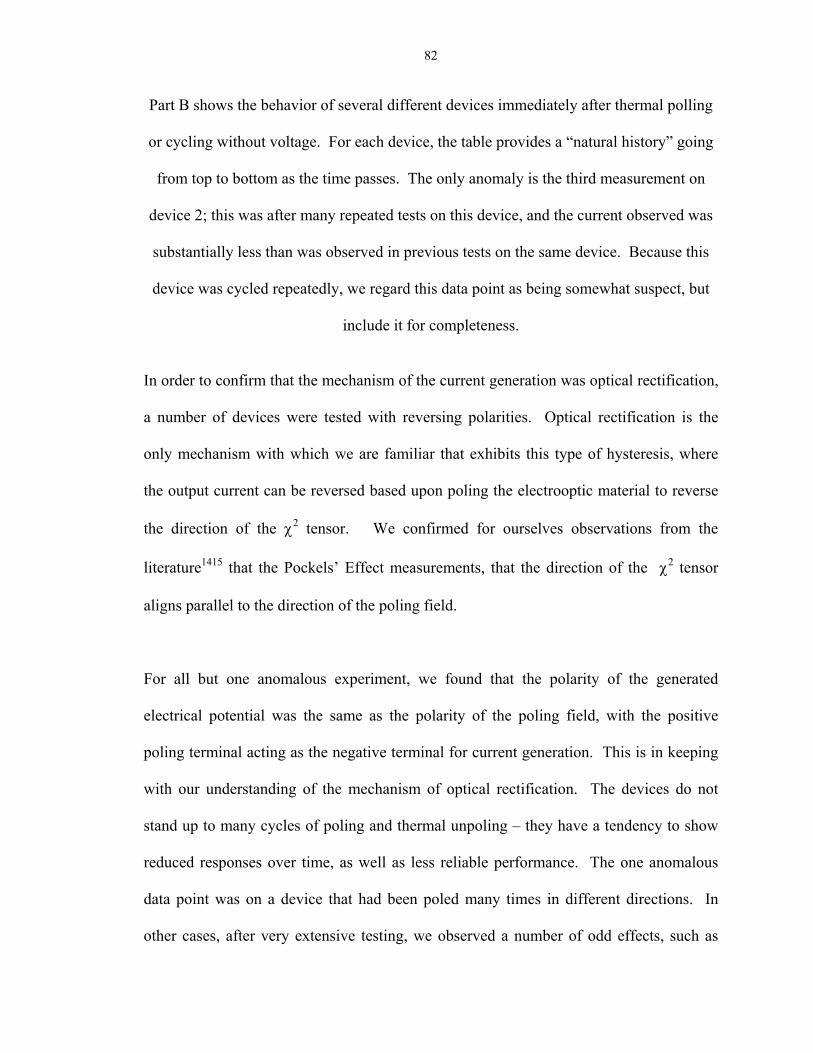
82
Part B shows the behavior of several different devices immediately after thermal polling
or cycling without voltage. For each device, the table provides a “natural history” going
from top to bottom as the time passes. The only anomaly is the third measurement on
device 2; this was after many repeated tests on this device, and the current observed was
substantially less than was observed in previous tests on the same device. Because this
device was cycled repeatedly, we regard this data point as being somewhat suspect, but
include it for completeness.
In order to confirm that the mechanism of the current generation was optical rectification,
a number of devices were tested with reversing polarities. Optical rectification is the
only mechanism with which we are familiar that exhibits this type of hysteresis, where
the output current can be reversed based upon poling the electrooptic material to reverse
the direction of the χ2 tensor. We confirmed for ourselves observations from the
literature1415 that the Pockels’ Effect measurements, that the direction of the χ2 tensor
aligns parallel to the direction of the poling field.
For all but one anomalous experiment, we found that the polarity of the generated
electrical potential was the same as the polarity of the poling field, with the positive
poling terminal acting as the negative terminal for current generation. This is in keeping
with our understanding of the mechanism of optical rectification. The devices do not
stand up to many cycles of poling and thermal unpoling – they have a tendency to show
reduced responses over time, as well as less reliable performance. The one anomalous
data point was on a device that had been poled many times in different directions. In
other cases, after very extensive testing, we observed a number of odd effects, such as

83
spontaneous switching of the polarity of the output current. Because of the complexity of
the interactions within these polymer-chromophore materials in nanoscale gaps, a
detailed model of the material behavior under the conditions prevailing in our devices is
not available at this time. This is a subject that bears further investigation.
Figure 5.19: Panel A shows the transmission spectrum of detector device 1, whereas B
shows detector device 2. Panel C shows several curves of current vs. power for three
measurement series. Series 1 is of the first device with the wavelength at1549.26 nm, on
a resonance peak. Series 2 is the first device with the wavelength at 1550.5 nm off
resonance. Series 3 is for device 2, with the wavelength at 1551.3, on resonance. Finally,
panel D shows the output current as a function of wavelength, overlaid with the

84
transmission spectrum. The transmission spectrum has been arbitrarily rescaled to show
the contrast.
A series of additional experiments were performed using a lock-in amplifier at 1 kHz, in
order to improve the signal-to-noise performance of the setup. In Figure 5.19,
transmission curves taken with the lock-in are shown. In analyzing this data, we consider
the relationship cPI = , where I is the output current, P is the input laser power, and c is
a proportionality constant. We determined with these experiments that on-resonance, c
took on a value of 88 +/- 10 pA/mW and off-resonance, a value of 58+/-8 pA/mW.
Figure 5.19 panel d shows change in the output current as the wavelength of the input
laser was tuned across several resonances. Clearly, where the system is tuned to a
resonance peak, the output current is at a max. The wavelength response is also shown
for clarity. Because of the low Q of the devices, there is some light in the resonator even
when the system is off-resonance, so a nonzero output power is unsurprising.
Measurements of the photoresponse of the devices were performed up to 1 MHz, with the
rolloff in their response being nearly perfectly modeled by the RLC response of the
system. This indicates that the limitation on the speed of these devices is not the
underlying mechanism of photoconversion, but rather the parasitics of the devices, which
can be easily improved through careful electrical design.

85
4.2 Analysis of data for optical rectification
We have shown elsewhere16 that the expected direction of the field resulting from optical
rectification is reversed in comparison to the direction of the 2χ moment of the material
in our gaps. This was found to be consistent with our observed data.
To derive the magnitude of the expected photocurrent, we assume that the 2χ magnitude
relating to the Pockels’ Effect is similar to that for optical rectification. A measurement
of 2χ can then be obtained from the direct observation of the electrooptic coefficient by
the standard measurements described earlier. The typical measured tuning value of
2GHz/V yields approximately 50 pm/V.
In the best case, devices with 6 dBm of input power returned approximately 1.4 nA of
current. With Q’s ranging from 3k to 5k, and assuming approximately 7 dB of insertion
loss in the input grating coupler on one of our chips, in the best case as much as 0 dBm
might be circulating in a resonator on resonance. This implies a peak electric field due to
the optical signal of approximately 3.1x10⁶ V/m. The induced static nonlinear
polarization field is then nearly 1000 V/m, which amounts to a voltage drop of 14x10-5 V
across a 140 nm gap. If this voltage is assumed to be perfectly maintained, and the load
resistance is assumed to be 5 MΩ, then 28 pA would be generated, about a factor of 100
less than is observed in the largest measurement made, but within a factor of 20 of the
typical measurement of 352 pA for 6 dBm of input. Significantly, because the generated
current is quadratic in E, it is clear that the current will be linearly proportional to the
input intensity. This is in accordance with our observations. The best results for optical

86
rectification were obtained with YLD/APC polymer, whereas our best Pockels’ Effect
results were obtained with the dendrimer materials.
Significantly, the sign of the output current matches that which would be predicted by
nonlinear optical rectification, as predicted in section 4.1. Specifically, since positive
current emanates from the positive terminal, the rectified E field has a sign reversed from
the 2χ and the polling E field. It should be noted that it is a well-established fact with
these materials that the 2χ direction tends to align with the direction of the polling E
field. Because of this, the rectified field acting as a voltage source will produce an
effective positive terminal at the terminal that had the positive polling voltage.
We do not yet fully understand the current generation mechanism. In particular, it is
not clear what provides the mechanism for charge transport across the gap. The APC
material in which the nonlinear polymer is hosted is insulating, and though it does exhibit
the photoconductivity effect due to visible light, it is unclear whether it can for near-
infrared radiation. Photoconductivity due to second-harmonic generation may play a role
in this effect. It is certainly the case, however, that current flows through this gap; that is
the only region in the entire system where an electromotive force exists. Also,
photoconductivity alone is not adequate to explain the reversal of the current coming off
of the detector devices when the poling direction is reversed, nor the conversion of the
optical input into directed current in general. The only mechanism to our knowledge that
adequately explains this data is optical rectification.\

87
If we assume that it will be possible to achieve a 10x improvement in the Q’s of the
resonators, while still getting more than 10 dB of extinction, then the intensity circulating
in such a ring would be about 13 dB up from the intensity of the input wave. By
comparison, with a Q of about 1000 and high extinction, the peak circulating intensity is
about the same as the intensity in the input waveguide. So it’s reasonable to expect that it
will be possible to get at least 10 dB of improvement in the circulating intensity, and thus
in the conversion efficiency, by fabricating higher-Q rings.
Because the optical losses of the polymer and dendrimer materials could turn out to be a
limiting factor for the performance of higher-Q devices, a thorough study of the optical
losses of these materials is needed. Because the devices used herein were deliberately
designed to have low Q’s, they are not the ideal system for examining such losses. It is
possible to say that an upper bound of about 10dB/cm of loss is reasonable, based on our
observations that the Q’s of the resonators did not change dramatically after being coated
with the organic materials. However, further work is clearly required to determine
whether the optical loss in these materials will prove to be a limiting factor in device
performance.
Conclusion
By means of our nanoscale slotted waveguide geometry, we have obtained massive
enhancement of both the optical field and of the electric field for low input voltage. This,
and the intrinsically high mode field concentration obtained with standard non-slot
waveguides, has enabled us to construct three new classes of devices: Hybrid silicon-

88
polymer tunable waveguides, slot-waveguide modulators, and microscale optical
rectification-based detectors. The first class of devices takes advantage of the high mode-
field concentration associated with silicon ring resonators in order to bring the electrodes
of a Pockels’ Effect modulator much closer together than could be realized in an all-
polymer system, allowing the construction of integrated 1x4x1 ROADM devices. The
slot ring resonator-based modulators take advantage of silicon’s ability to become
conductive through doping without inducing devastating optical losses. These devices
break the fundamental spacing-voltage-loss tradeoff traditionally associated with
Pockels’ Effect devices, since they use the two sides of the slot waveguide as
independent electrodes to both pole and modulate the devices. The detectors take
advantage of both the high electric fields across the gap and the high concentration of the
optical mode in order to create a fundamentally novel class of optical detector, allowing
us to exploit nonlinear optical processes that are typically only available in the kW
regime in the sub-mW regime.
This difference is so considerable that we believe it represents a change in kind for the
function of nonlinear optical devices; it may be possible to someday construct a practical,
low-power detector based purely on nonlinear optical rectification. In addition, we
expect this hybrid material system to provide a means for creating compact devices that
exploit other nonlinear phenomena on-chip. Many of the functions, such as frequency
conversion, that today are largely served by periodically poled lithium niobate, may
eventually be served by massively integrated silicon-on-insulator slot waveguides like the
ones demonstrated herein.

89
Optical rectification-based detectors might have many advantages over currently
available technology. In particular, such detectors would probably be able to function at a
higher intrinsic rate than the typical photodiode as the optical rectification process occurs
at the optical frequency itself, on the order of 100 THz in WDM systems. The absence of
an external bias, and the generation of a voltage rather than a change in current flow,
might also prove easier to handle electronically. We also do not believe that a device
based on nonlinear optical rectification would suffer from the limitation of a dark current,
though there certainly may be other noise-generating processes. Because of the lack of
external bias, it seems likely that leakage current is simply not going to be a limiting
factor for these detectors. This in turn might mean that current WDM systems could
function with lower optical power, providing numerous benefits. We are particularly
optimistic that these detectors might, in the short term, provide a replacement for long-
wavelength photomultiplier tubes, which are both quite slow and very insensitive. The
processes that underlie the rectification detection scheme are fairly insensitive to the
wavelength of the light being detected, and we expect that such devices could easily be
extended into the mid-wave infrared at the very least. Similarly, our demonstration of
enhanced modulation using these waveguide geometries may also lead to useful
components in future communications systems. We expect that with increased ring
quality factors and/or other cavity designs that optimize the peak electric field associated
with the optical mode, these detectors can be made dramatically more efficient.
We conclude by stressing the economic aspects of our development. Because our devices
can be fabricated in planar, electronics-grade silicon-on-insulator, using processes

90
compatible with advanced CMOS processing, it is likely the devices based on these
principles could be built cheaply. It is our hope that electrically active slotted waveguides
can someday become a platform of choice for practical linear and nonlinear integrated
optics.
1 P. Rabiei, W. Steier, C. Zhang, and L.. Dalton. “Polymer Micro-Ring Filters and Modulators.” J. Lightwave Technology 20, (11) 1968 (2002) 2 B. Saleh, M. Teich. “Fundamentals of Photonics.” New York: John Wiley and Sons, 1991. 3 B. Saleh, M. Teich. “Fundamentals of Photonics.” New York: John Wiley and Sons, 1991. 4 Q. F. Xu, V. R. Almeida, R. R. Panepucci, M. Lipson, “Guiding and Confining Light in Void Nanostructures,” Opt. Lett. 29, 1206-1211 (2004). 5 Unpublished Communications. 6 A. Wolfe and G. Zissis, “The Infrared Handbook,” Ann Arbor, MI: Environmental Research Institute of Michigan, 1989. 7 R. Sosran, Properties of Silica, New York: American Chemical Soc., 1927. 8 Q. F. Xu, V. R. Almeida, R. R. Panepucci, M. Lipson, “Guiding and Confining Light in Void Nanostructures,” Opt. Lett. 29, 1206-1211 (2004). 9 T. Baehr-Jones, M. Hochberg, C. Walker, A Scherer, "High-Q optical resonators in silicon-on-insulator-based slot waveguides," Appl. Phys. Lett. 86, 081101 (2005). 10 C. Zhang, L. R. Dalton, M. C. Oh, H. Zhang, W. H. Steier, “Low V-pi electrooptic modulators from CLD-1: Chromophore design and synthesis, material processing, and characterization,” Chem. Mater. 13, 3043-3050 (2001). 11 P. Rabiei, W. Steier, C. Zhang, and L.. Dalton. “Polymer Micro-Ring Filters and Modulators.” J. Lightwave Technology 20, (11),1968 (2002) 12 M. Bass, P. A. Franken, J. F. Ward, G. Weinreich, “Optical Rectification,” Phys. Rev. Lett. 9, 446 (1962). 13 A. Nahata, D. H. Auston, C. J. Wu, J. T. Yardley, “Generation of Terahertz Radiation From a Poled polymer,” Appl. Phys. Lett., 67, 1358-1360 (1995). 14 Zhang, L. R. Dalton, M. C. Oh, H. Zhang, W. H. Steier, “Low V-pi electrooptic modulators from CLD-1: Chromophore design and synthesis, material processing, and characterization,” Chem. Mater. 13, 3043-3050 (2001). 15 S. Graf, H. Sigg, W. Bachtold, “High-frequency electrical pulse generation using optical rectification in bulk GaAs,” Appl. Phys. Lett. 76, 2647-2649 (2000). 16 T. Baehr-Jones, M. Hochberg, G. Wang, R. Lawson, Y. Liao, P. Sullivan, L. Dalton, A. Jen, and A. Scherer, "Optical modulation and detection in slotted Silicon waveguides," Opt. Express 13, 5216-5226 (2005)

91
6. Conclusion
The work described herein has been primarily an effort to expand in scope the type of
experiments performed in silicon-on-insulator optics to include ultrafast nonlinear effects.
Because of the unique properties of highly confined SOI waveguides – ready
manufacturability, ease of integration with electronics, inexpensive fabrication and
packaging, high mode-field concentration, and low loss – they provide an intriguing
material system for the construction of nonlinear optical devices. We have developed a
library of optical components that can all be integrated into the same substrates and
waveguide geometries as low-loss, high-confinement silicon waveguides. By utilizing
evanescently coupled nonlinear polymer cladding, the effective nonlinearity of the optical
waveguides can be improved, yielding a compelling new hybrid materials approach to
integrated nonlinear optics.
Because of the ease of producing devices with many different sub-components, it is
possible to construct extremely compact and complex optical devices. It is my hope that
this will lead to the construction of devices exhibiting ultrafast signal gain. Given that
free-carrier optical transmitters and receivers are currently being commercialized in
foundry silicon processes, it is likely that an infrastructure will soon exist for building
low-loss, highly repeatable optical devices commercially. By taking advantage of this to
do nonlinear optics, I hope that it will become possible to commercialize nonlinear
optical components that replace benchtop free-space optics with on-chip nonlinearities,
realizing a two-orders-of-magnitude or more cost savings.

92
In addition, many of the waveguide structures that we have developed are likely to be
useful for the construction of sensors. In particular, we are optimistic that the slot ring
resonators (or perhaps interferometers) will provide an interesting new platform for
evanescent optical environmental sensors, particularly as the contacts will allow fast
temperature control in order to force species to desorb from the surfaces.
There are several obvious directions in which the research described in this thesis can be
extended. First of all, the efficiency and speed of the optical rectification-based detectors
can be greatly enhanced through both clever electrical design and through resonant
enhancement. The ultrafast modulators are also likely to benefit from resonant
enhancement, as well as more optimized polymers. Furthermore, it seems likely that it
will be possible, perhaps by using silicon-on-sapphire or metal waveguides to reduce
substrate losses at long wavelengths, to demonstrate sum- and difference-frequency
generation in highly confined silicon-based systems. Finally, I believe that it will turn
out to be worth exploring the limits of using silicon by itself, without polymer claddings,
to produce nonlinearities; it is possible the power and field handling of the silicon alone
will turn out to be so substantially better than today’s polymers that silicon-only resonant
structures can be extended to the regime of larger nonlinearities, where the polymers
cannot follow due to breakdown issues. I am hopeful that novel materials, be they
polymers or others, will enable much larger ultrafast optical nonlinearities in the near
future, perhaps leading to all-optical ultrafast logic.

93
Appendix A – Random Interesting Micrographs There are some decent images of working devices that made it into the body of this work.
I thought that it would be worth showing some of the interesting images of devices that
didn’t work, or that didn’t come out the way I expected, or that just happen to look
interesting. After all, for every good device, at least ten got made and didn’t come out.
Nanofabrication is the art of turning beautiful grant money into broken silicon.
Figure A.1: Some early electrical contact structures for slot ring resonators.

94
Figure A.2: An undercut silicon waveguide imaged from the top.
Figure A.3: An early slot waveguide contact structure after wet chemical resist removal.
The intermediate grating structures have lifted off and redeposited.

95
Figure A.4: Proximity effect loading on an etched contact structure.
Figure A.5: A photonic crystal cavity with attached feed waveguides.

96
Figure A.6: Overetched resist in a test structure.
Figure A.7: Rough sidewalls on an optical structure.

97
Figure A.8: More rough sidewalls.
Figure A.9: The result of an improperly calibrated electron beam system. The
waveguide shows each subfield-stitch boundary. Subfield biases need recalibration!

98
Figure A.10: More subfield stitch boundaries, this time on a test structure. The white
lines are the shape boundaries.
Figure A.11: An early plasmon structure, where the silicon was overetched and the metal
didn’t lift off properly.

99
Figure A.12: Something went badly wrong here – perhaps underexposure and overetch
in XeF2, though it’s hard to be certain.
Figure A.13: A truly severe case of trapezium gain error – this was supposed to be one
continuous line.

100
Figure A.14: An AFM image of a photonic crystal cavity with waveguides.
Figure A.15: Subfield stitching errors are clearly shown at the edge of the input
waveguide in this micrograph. Such errors can be devastating for waveguide loss.