i.mx6qseven pmic som hardware user guide systems technologies/… · rel 1.2 page 3 of 82 i.mx6...
TRANSCRIPT

REL 1.2 Page 1 of 82
i.MX6 Qseven PMIC SOM Hardware User Guide
iWave Systems Technologies Pvt. Ltd.
iW-RainboW-G15M i.MX6 Qseven PMIC SOM
Hardware User Guide

REL 1.2 Page 2 of 82
i.MX6 Qseven PMIC SOM Hardware User Guide
iWave Systems Technologies Pvt. Ltd.
Document Revision History
Document Number iW-PRDVZ-UM-01-R5.0-REL1.2-Hardware
Revision Date Description
1.0 11th Sep 2014 Official Release Version
1.1 28th Jan 2015 Qseven Edge connector pin details are udpated in Table 5 for pins 20,28,120,121,
154 & 204
Heat spreader part number for i.MX6DL/S Qseven PMIC SOM is updated in ORDERING INFORMATION
Figure 15 and Figure 16 are updated with tolerance information
Table 17 updated with Power consumption details
1.2 07th Mar 2016 Table 8 PMIC OTP Header pinout detail is corrected
Table 11 Debug UART Header pinout detail is corrected
Important Note is added below Table 16 for power sequencing related
i.MX6 QuadPlus and DualPlus CPU supported Qseven SOM part numbers are updated in ORDERING INFORMATION
2GB RAM supported Qseven SOM part numbers are updated in ORDERING INFORMATION
PROPRIETARY NOTICE: This document contains proprietary material for the sole use of the intended recipient(s). Do
not read this document if you are not the intended recipient. Any review, use, distribution or disclosure by others
is strictly prohibited. If you are not the intended recipient (or authorized to receive for the recipient), you are
hereby notified that any disclosure, copying distribution or use of any of the information contained within this
document is STRICTLY PROHIBITED. Thank you. “iWave Systems Tech. Pvt. Ltd.”

REL 1.2 Page 3 of 82
i.MX6 Qseven PMIC SOM Hardware User Guide
iWave Systems Technologies Pvt. Ltd.
Disclaimer
iWave Systems reserves the right to change details in this publication including but not limited to any Product
specification without notice.
No warranty of accuracy is given concerning the contents of the information contained in this publication. To the
extent permitted by law no liability (including liability to any person by reason of negligence) will be accepted by
iWave Systems, its subsidiaries or employees for any direct or indirect loss or damage caused by omissions from or
inaccuracies in this document.
CPU and other major components used in this product may have several silicon errata associated with it. Under no
circumstances, iWave Systems shall be liable for the silicon errata and associated issues.
Trademarks
All registered trademarks, product names mentioned in this publication are the property of their respective owners
and used for identification purposes only.
Certification
iWave Systems Technologies Pvt. Ltd. is an ISO 9001:2008 Certified Company.
Warranty & RMA
Warranty support for Hardware: 1 Year from iWave or iWave's EMS partner.
For warranty terms, go through the below web link,
http://www.iwavesystems.com/support/warranty.html
For Return Merchandise Authorization (RMA), go through the below web link,
http://www.iwavesystems.com/support/rma.html
Technical Support
iWave Systems technical support team is committed to provide the best possible support for our customers so that
our Hardware and Software can be easily migrated and used.
For assistance, contact our Technical Support team at,
Email : [email protected]
Website : www.iwavesystems.com
Address : iWave Systems Technologies Pvt. Ltd.
# 7/B, 29th Main, BTM Layout 2nd Stage,
Bangalore, Karnataka,
India – 560076

REL 1.2 Page 4 of 82
i.MX6 Qseven PMIC SOM Hardware User Guide
iWave Systems Technologies Pvt. Ltd.
Table of Contents
1. INTRODUCTION ............................................................................................................................................ 7
1.1 Purpose ............................................................................................................................................................. 7
1.2 Qseven SOM Overview ..................................................................................................................................... 7
1.3 List of Acronyms ................................................................................................................................................ 7
1.4 Terminlogy Description ..................................................................................................................................... 9
1.5 References ........................................................................................................................................................ 9
1.6 Important Note ............................................................................................................................................... 10
2. ARCHITECTURE AND DESIGN ....................................................................................................................... 11
2.1 i.MX6 Qseven PMIC SOM Block Diagram ........................................................................................................ 11
2.2 i.MX6 Qseven PMIC SOM Features ................................................................................................................. 12
2.3 i.MX6 CPU ....................................................................................................................................................... 14
2.4 PMIC ................................................................................................................................................................ 15
2.5 Boot Switches .................................................................................................................................................. 15
2.5.1 Boot Mode Switch ....................................................................................................................................... 16
2.5.2 Boot Media Setting Switch .......................................................................................................................... 17
2.6 Memory ........................................................................................................................................................... 18
2.6.1 DDR3 SDRAM .............................................................................................................................................. 18
2.6.2 SPI NOR Flash .............................................................................................................................................. 18
2.6.3 eMMC Flash ................................................................................................................................................ 18
2.6.4 Micro SD Slot ............................................................................................................................................... 18
2.7 Qseven PCB Edge Connector .......................................................................................................................... 19
2.7.1 PCIe Interface .............................................................................................................................................. 20
2.7.2 Data UART Interface (UART5) ..................................................................................................................... 20
2.7.3 Gigabit Ethernet Interface ........................................................................................................................... 20
2.7.4 SATA Interface ............................................................................................................................................. 21
2.7.5 USB 2.0 Host Interface ................................................................................................................................ 21
2.7.6 USB 2.0 OTG Interface ................................................................................................................................. 22
2.7.7 SD/MMC Interface ...................................................................................................................................... 22
2.7.8 AC’97/I2S Audio Interface ........................................................................................................................... 22
2.7.9 LVDS Display Interface ................................................................................................................................ 23
2.7.10 HDMI Interface ............................................................................................................................................ 23
2.7.11 LPC/GPIO Interface ...................................................................................................................................... 24
2.7.12 SPI Interface ................................................................................................................................................ 24
2.7.13 CAN Interface .............................................................................................................................................. 24
2.7.14 Power Input ................................................................................................................................................. 25
2.7.15 Power Control Signals ................................................................................................................................. 25
2.7.16 Power Management Signals ....................................................................................................................... 25
2.7.17 PWM Interface ............................................................................................................................................ 26
2.7.18 WDOG Interface .......................................................................................................................................... 26
2.7.19 I2C Interface ................................................................................................................................................ 26
2.7.20 Manufacturing/Debug UART Interface (UART2) ......................................................................................... 26

REL 1.2 Page 5 of 82
i.MX6 Qseven PMIC SOM Hardware User Guide
iWave Systems Technologies Pvt. Ltd.
2.8 Expansion Connector1 Interfaces ................................................................................................................... 42
2.8.1 Parallel LCD Display Interface ..................................................................................................................... 43
2.8.2 MIPI DSI Interface........................................................................................................................................ 43
2.8.3 Parallel Camera Interface1 ......................................................................................................................... 43
2.8.4 ESAI Interface .............................................................................................................................................. 44
2.8.5 SPDIF Interface ............................................................................................................................................ 44
2.8.6 Data UART Interface (UART1 & UART3) ...................................................................................................... 44
2.9 Expansion Connector2 Interfaces ................................................................................................................... 51
2.9.1 Parallel Camera Interface2 ......................................................................................................................... 52
2.9.2 MIPI CSI Interface ........................................................................................................................................ 52
2.9.3 Memory Bus Interface ................................................................................................................................. 53
2.9.4 Keypad Interface ......................................................................................................................................... 53
2.9.5 Data UART Interface (UART4) ..................................................................................................................... 53
2.9.6 MLB Interface .............................................................................................................................................. 53
2.10 Optional Features ........................................................................................................................................... 60
2.10.1 NAND Flash ................................................................................................................................................. 60
2.10.2 RTC Controller ............................................................................................................................................. 60
2.10.3 PMIC OTP Header ........................................................................................................................................ 61
2.10.4 JTAG Header ................................................................................................................................................ 62
2.10.5 Debug UART Header.................................................................................................................................... 64
2.10.6 Power IN Connector .................................................................................................................................... 65
3. TECHNICAL SPECIFICATION.......................................................................................................................... 66
3.1 Electrical Characteristics ................................................................................................................................. 66
3.1.1 Power Input Requirement ........................................................................................................................... 66
3.1.2 Power Input Sequencing .............................................................................................................................. 67
3.1.3 Power Consumption .................................................................................................................................... 68
3.2 Environmental Characteristics ........................................................................................................................ 69
3.2.1 Environmental Specification ........................................................................................................................ 69
3.2.2 Heat Spreader ............................................................................................................................................. 69
3.2.3 RoHS Compliance ........................................................................................................................................ 70
3.2.4 Electrostatic Discharge ................................................................................................................................ 70
3.3 Mechanical Characteristics ............................................................................................................................. 71
3.3.1 Qseven SOM Mechanical Dimensions ......................................................................................................... 71
3.3.2 Guidelines to insert the Qseven SOM into Carrier board ............................................................................ 73
4. ORDERING INFORMATION .......................................................................................................................... 74
5. MIGRATION INFORMATION ........................................................................................................................ 78
6. APPENDIX I ................................................................................................................................................. 80
6.1 i.MX6 Qseven PMIC SOM Silk Screen ............................................................................................................. 80
7. APPENDIX II ................................................................................................................................................ 82
7.1 i.MX6 Qseven PMIC SOM Development Platform .......................................................................................... 82

REL 1.2 Page 6 of 82
i.MX6 Qseven PMIC SOM Hardware User Guide
iWave Systems Technologies Pvt. Ltd.
List of Figures
Figure 1: i.MX6 Qseven SOM Block Diagram .................................................................................................................. 11
Figure 2: i.MX6Q Simplified Block Diagram .................................................................................................................... 14
Figure 3: Boot Switches ................................................................................................................................................... 15
Figure 4: Micro SD Slot .................................................................................................................................................... 18
Figure 5: Qseven PCB Edge Connector............................................................................................................................ 19
Figure 6: Expansion Connector1 ..................................................................................................................................... 42
Figure 7: Expansion Connector1 ..................................................................................................................................... 51
Figure 8: PMIC OTP Header ............................................................................................................................................. 61
Figure 9: JTAG Header ..................................................................................................................................................... 62
Figure 10: Debug UART Header ...................................................................................................................................... 64
Figure 11: 2Pin Power Connector ................................................................................................................................... 65
Figure 12: Qseven SOM Power Sequence ....................................................................................................................... 67
Figure 13: Heat Spreader Dimensions ............................................................................................................................ 70
Figure 14: Mechanical dimension of Qseven SOM- Top View ........................................................................................ 71
Figure 15: Mechanical dimension of Qseven SOM- Bottom View .................................................................................. 72
Figure 16: Mechanical dimension of Qseven SOM- Side View ....................................................................................... 72
Figure 17: Qseven Module Insertion procedure ............................................................................................................. 73
Figure 18: Silk Screen Top View ...................................................................................................................................... 80
Figure 19: Silk Screen Bottom View ................................................................................................................................ 81
Figure 20: i.MX6 Qseven PMIC SOM Development Platform ......................................................................................... 82
List of Tables
Table 1: Acronyms & Abbreviations .................................................................................................................................. 7
Table 2: Terminology ........................................................................................................................................................ 9
Table 3: Boot Mode Settings Truth Table ....................................................................................................................... 16
Table 4: Compatible Magnetics ...................................................................................................................................... 21
Table 5: 230-Pin PCB Edge Connector Pin Assignment ................................................................................................... 27
Table 6: Expansion Connector1 Pin Assignment ............................................................................................................. 45
Table 7: Expansion Connector2 Pin Assignment ............................................................................................................. 54
Table 8: PMIC OTP Header Pin Assignment .................................................................................................................... 61
Table 9: JTAG Header Pin Assignment ............................................................................................................................ 62
Table 10: JTAG Header - BOM ......................................................................................................................................... 63
Table 11: Debug UART Header Pin Assignment .............................................................................................................. 64
Table 12: Debug UART Header - BOM ............................................................................................................................ 64
Table 13: 2Pin Power Connector ..................................................................................................................................... 65
Table 14: Power IN Connector - BOM ............................................................................................................................. 65
Table 15: Power Input Requirement ............................................................................................................................... 66
Table 16: Power Sequence Timing .................................................................................................................................. 67
Table 17: Power Consumption¹ ....................................................................................................................................... 68
Table 18: Environmental Specification ........................................................................................................................... 69
Table 19: Orderable Product Part Numbers ................................................................................................................... 74
Table 20: Differences between i.MX6 Qseven Non PMIC SOM and i.MX6 Qseven PMIC SOM ..................................... 78

REL 1.2 Page 7 of 82
i.MX6 Qseven PMIC SOM Hardware User Guide
iWave Systems Technologies Pvt. Ltd.
1. INTRODUCTION
1.1 Purpose
This document is the Hardware User Guide for the i.MX6 Qseven System On Module based on the Freescale’s i.MX6
Applications Processor with PMIC. This board is fully supported by iWave Systems Technologies Pvt. Ltd. This Guide
provides detailed information on the overall design and usage of the i.MX6 Qseven System On Module from a
Hardware Systems perspective.
1.2 Qseven SOM Overview
The Qseven concept is an off-the-shelf, multi-vendor, Single-Board-Computer that integrates all the core
components of a common PC and is mounted onto an application specific carrier board. Qseven modules have a
standardized form factor of 70mm x 70mm and have specified pin outs based on the high speed MXM system
connector that has a standardized pin out regardless of the vendor. A single ruggedized MXM connector provides the
carrier board interface to carry all the I/O signals to and from the Qseven module.
1.3 List of Acronyms
The following acronyms will be used throughout this document.
Table 1: Acronyms & Abbreviations
Acronyms Abbreviations
ARM Advanced RISC Machine
BOM Bill of Material
BPP Bits Per Pixel
BSP Board Support Package
CAN Controller Area Network
CEC Consumer Electronics Control
CPU Central Processing Unit
CSI Camera Serial Interface
DDR3 Double Data Rate 3
DSI Display Serial Interface
DVI Digital Visual Interface
eCSPI Enhanced Configurable Serial Peripheral Interface
eMMC Enhanced Multi Media Card
ESAI Enhanced Serial Audio Interface
FLEXCAN Flexible Controller Area Network
GB Giga Byte
Gbps Gigabits per sec
GPIO General Purpose Input Output
HDCP High-bandwidth Digital Content Protection

REL 1.2 Page 8 of 82
i.MX6 Qseven PMIC SOM Hardware User Guide
iWave Systems Technologies Pvt. Ltd.
Acronyms Abbreviations
HDMI High-Definition Multimedia Interface
I2C Inter-Integrated Circuit
IC Integrated Circuit
IPU Image Processing Unit
JTAG Joint Test Action Group
Kbps Kilobits per second
LCD Liquid Crystal Display
LDB LVDS Display Bridge
LVDS Low Voltage Differential Signal
MAC Media Access Controller
MB Mega Byte
Mbps Megabits per sec
MHz Mega Hertz
MIPI Mobile Industry CPU Interface
MLB Media Local Bus
MMC Multi Media Card
NC No Connect
NPTH Non Plated Through hole
PCB Printed Circuit Board
PMIC Power Management Integrated Circuit
PTH Plated Through hole
PWM Pulse Width Modulation
RGMII Reduced Gigabit Media Independent Interface
ROM Read-Only Memory
RTC Real Time Clock
SATA Serial Advanced Technology Attachment
SD Secure Digital
SDIO Secure Digital Input Output
SDRAM Synchronous Dynamic Random Access Memory
SOM System On Module
SPDIF Sony/Philips Digital Interconnect Format
SPI Serial Peripheral Interface
SSI Synchronous Serial Interface
TMDS Transition Minimized Differential Signalling
UART Universal Asynchronous Receiver/Transmitter
USB Universal Serial Bus
USB OTG USB On The Go

REL 1.2 Page 9 of 82
i.MX6 Qseven PMIC SOM Hardware User Guide
iWave Systems Technologies Pvt. Ltd.
1.4 Terminlogy Description
In this document, wherever Signal Type is mentioned, below terminology is used.
Table 2: Terminology
Terminology Description
I Input Signal
O Output Signal
IO Bidirectional Input/output Signal
CMOS Complementary Metal Oxide Semiconductor Signal
LVDS Low Voltage Differential Signal
TMDS Transition Minimized Differential Signal
DIFF Differential Signal
OD Open Drain Signal
OC Open Collector Signal
RS232 RS-232 compatible Signal
Power Power Pin
PU Pull Up
PD Pull Down
NA Not Applicable
NC Not Connected
Important Note: Signal Type does not include internal pull-ups or pull-downs implemented by the chip vendors and
only includes the pull-ups or pull-downs implemented On-SOM.
1.5 References
i.MX6 Applications Processors Datasheet
i.MX6 Applications Processors Reference Manual
i.MX6 Applications Processors Hardware Development Guide
Qseven® Specification Version 2.0
Qseven® Design Guide

REL 1.2 Page 10 of 82
i.MX6 Qseven PMIC SOM Hardware User Guide
iWave Systems Technologies Pvt. Ltd.
1.6 Important Note
In this document, wherever i.MX6 CPU signal name is mentioned, it is followed as per below format.
If CPU pin functionality name and CPU pad name is same, Signal name is mentioned as
“CPU Pad Name”
Example: SD3_DATA2
In this signal, functionality which we are using and CPU Pad name is SD3_DATA2.
If CPU pin functionality name and pad name is different, Signal name is mentioned as
“Functionality name (CPU Pad name)”
Example: UART3_RTS(SD3_RST)
In this signal, UART3_RTS is the functionality which we are using and SD3_RST is the CPU Pad name.
If CPU pin functionality is GPIO, Signal name is mentioned as
“GPIO Number_FunctionalityDescription (CPU Pad name)”
Example: GPIO7_0_SD1_CD(SD3_DAT5)
In this signal, GPIO7_0 is the GPIO number, SD1_CD (SD1 card detect) is the functionality which we are using
and SD3_DAT5 is the CPU pad name.
Note: The above naming is not applicable for other signals which are not connected to CPU.

REL 1.2 Page 11 of 82
i.MX6 Qseven PMIC SOM Hardware User Guide
iWave Systems Technologies Pvt. Ltd.
2. ARCHITECTURE AND DESIGN
This section provides detailed information about the i.MX6 Qseven PMIC SOM Features and Hardware architecture
with high level block diagram. Also this section provides detailed information about Qseven edge connector &
Expansion connector’s pin assignment and usage.
2.1 i.MX6 Qseven PMIC SOM Block Diagram
CPUi.MX6
DDR3 RAM
SPI NOR Flash
eMMC
PCIe x 1
QSEVEN PCB Edge
Connector(230Pin)
SATA x 1
USBOTG x 1
USB Host x 4USB Host x 1
LVDS x 2, PWM x1
HDMI x 1
Gbit EthernetRGMII x 1
SD/MMC (8bit) x 1
I2C x 2
SPI x 1 (2 Chip selects)
CAN x 1, Data UART x 1
WDOGn
8 GPIOs, Status & Control Signals
PCIe Bus
SATA II 3.0Gbos
USB OTG HS PHY
USB HOST1 HS PHY
LVDS0, LVDS1,PWM
HDMI 1.4
10/100/1000
ENET
eSDHC1
eCSPI2
CAN1,UART5
WDOG1
GPIOs
MMC (8bit)
SPI
DDR3 (64bit)
Micro SDConnector
SD (4bit)
Expansion Connector1
(80Pin header)
USB 2.0 Hub (4Port)
Gigabit Ethernet PHY
MMDC
eCSPI1
eSDHC4
eSDHC3
Audio x 1AUDMUX4
UART2
LCD (24bpp) x 1, MIPI-DSI x 1 DISP0,MIPI DSI
UART1,UART3
ESAI, SPDIF
CSI1
KPP
UART (with CTS & RTS) x 2
ESAI x 1, SPDIF x 1
Camera2 (8bit) x 1
Keypad 3x3
3Pin Header (Optional)
SJC
iW-RainboW-G15M-i.MX6 Qseven PMIC SOM Block Diagram
MLBMLB x 1
EIMMemory Bus (Address/Data Muxed)
Note: * MLB is supported only in Automotive part.
UART x 1
2Pin Power In(Optional)
JTAG
Power to Peripherals
5V
Debug
CSI0Camera1 (8bit) x 1
JTAG (Optional) (20 Pin Header)
PMIC
RS232 Transceiver(Optional)
Dual SPDT Switch IC(Optional)
Expansion Connector2
(80Pin header)
MIPI CSIMIPI-CSI x 1
UART4UART x 1
I2C3I2C3 x 1
Single BitInverter
WDOG
Nand Flash (Optional)
I2C1, I2C2
RTC controller
(Optional)
Figure 1: i.MX6 Qseven SOM Block Diagram

REL 1.2 Page 12 of 82
i.MX6 Qseven PMIC SOM Hardware User Guide
iWave Systems Technologies Pvt. Ltd.
2.2 i.MX6 Qseven PMIC SOM Features
The i.MX6 Qseven PMIC SOM supports the following features.
CPU
Freescale’s i.MX6 QuadPlus/Quad/DualPlus/Dual/Duallite/Solo ARM™ Cortex-A9 based CPU @ up to
1GHz/Core
PMIC
Freescale’s MMPF0100 PMIC
Boot Switches
Boot Mode Setting Switch
Boot Media Setting Switch
Memory
1GB DDR3 RAM (Expandable)
2MB SPI NOR Flash (Expandable)
4GB eMMC Flash (Expandable)
Micro SD slot
Network & Communication
Gigabit Ethernet PHY transceiver
USB 2.0 High Speed 4-Port Hub
Qseven PCB Edge Interfaces
PCIe Gen2.0 x 1 Port
Data UART x 1 Port
Gigabit Ethernet x 1 Port (through On-SOM Gigabit Ethernet PHY transceiver)
SATA II (3.0 Gbps) x 1 Port
USB Host 2.0 x 4 Ports (through On-SOM USB 2.0 High Speed 4-port Hub)
USB OTG 2.0 x 1 Port
SD/MMC (8bit) x 1 Port
AC’97 or I2S Audio x 1 Port
LVDS x 2 Port
HDMI 1.4 x 1 Port
GPIOs x 8

REL 1.2 Page 13 of 82
i.MX6 Qseven PMIC SOM Hardware User Guide
iWave Systems Technologies Pvt. Ltd.
SPI x 1 Port (with 2 Chip selects )
CAN x 1 Port
Power control & Management signal
PWM x 1 Port
WDOG
I2C x 2 Ports
Debug UART
Expansion Connector1 Interfaces
Parallel LCD – 24bpp RGB x 1 Port
Dual Lane MIPI DSI
Parallel Camera1 (8bit) x 1 Port
ESAI x 1 Port
SPDIF x 1 Port
Data UART (with CTS & RTS) x 2 Ports
Expansion Connector2 Interfaces
Parallel Camera2 (8bit) x 1 Port
Four Lane MIPI CSI
Memory Bus (Address & Data Multiplexed) x 1 Port
Keypad Interface (3x3)
Data UART x 1 Port
MLB x 1 Port
Optional Features
NAND Flash
RTC Controller
PMIC OTP Header
JTAG Header
Debug UART Header for Standalone usage
Power IN Connector for Standalone usage
General Specification
Power Supply : 5V, 2A
Form Factor : 70mm X 70mm (Qseven R2.0 Specification)

REL 1.2 Page 14 of 82
i.MX6 Qseven PMIC SOM Hardware User Guide
iWave Systems Technologies Pvt. Ltd.
2.3 i.MX6 CPU
i.MX6 Qseven PMIC SOM is based on Freescale’s i.MX6 QuadPlus/Quad/DualPlus/Dual/Duallite/Solo ARM™ Cortex-
A9 core based CPU which can operate up to 1 GHz speed/core. i.MX6 CPU is Freescale’s latest achievement in
integrated multimedia application processors which is part of growing multimedia-focused products that offers high
performance processing and are optimized for lowest power consumption. The Block Diagram of i.MX6Q/D CPU
from the Freescale’s i.MX6Q/D datasheet is shown below for your reference.
Figure 2: i.MX6Q Simplified Block Diagram
Note: Please refer the latest i.MX6 Datasheet & Reference Manual from Freescale website for Electrical
characteristics of i.MX6 Application CPU which may be revised from time to time.

REL 1.2 Page 15 of 82
i.MX6 Qseven PMIC SOM Hardware User Guide
iWave Systems Technologies Pvt. Ltd.
2.4 PMIC
i.MX6 Qseven PMIC SOM supports Freescale’s MMPF0100 PMIC for On-SOM power management. The PMIC
provides all required power to i.MX6 CPU and all On SOM peripherals with programmable power management
solutions. This PMIC supports up to six buck converters, six linear regulators, RTC supply and coin-cell charger with
programmable output voltage, sequence and timing. i.MX6 CPU’s I2C2 interface is used for PMIC programmable. I2C
address for PMIC is 0x08.
2.5 Boot Switches
i.MX6 CPU boot process begins at Power On Reset (POR) where the hardware reset logic forces the ARM core to
begin execution starting from the on-chip boot ROM. i.MX6 CPU Boot ROM code uses the state of the internal
register BOOT_MODE [1:0] as well as the state of various eFUSEs and/or GPIO settings to determine the boot flow
behaviour of the device.
i.MX6 Qseven PMIC SOM supports two Boot switches for selecting Boot Mode setting and Boot Media setting of
i.MX6 CPU.
Boot Mode Setting Switch
Boot Media Setting Switch
Figure 3: Boot Switches

REL 1.2 Page 16 of 82
i.MX6 Qseven PMIC SOM Hardware User Guide
iWave Systems Technologies Pvt. Ltd.
2.5.1 Boot Mode Switch
i.MX6 Qseven PMIC SOM supports two positions Boot Mode Switch (SW2) which is physically located in the top of
the PCB. This switch is used to select the boot mode setting of i.MX6 CPU as explained in the below table.
Table 3: Boot Mode Settings Truth Table
Boot Mode Setting On
i.MX6 Qseven PMIC SOM Description
SW2 (2 Position Switch)
POS1 POS2 Image
Internal Boot Mode
(Default)
In this mode, i.MX6 boot media is
selected by GPIO Pin’s settings. OFF ON
Boot From eFuses
In this mode, i.MX6 boot media is
selected by i.MX6 eFUSE settings.
Note: i.MX6 eFuse setting is not
modified by iWave from silicon
shipped value.
OFF OFF
Serial Downloader Mode
In this mode, i.MX6 boot device
can be Programmed through its
USB OTG interface using MFG Tool.
ON ON
ON - High OFF - Low
REL 1.2 Page 17 of 82
i.MX6 Qseven PMIC SOM Hardware User Guide
iWave Systems Technologies Pvt. Ltd.
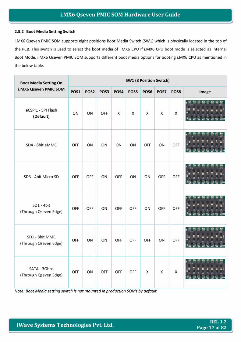
2.5.2 Boot Media Setting Switch
i.MX6 Qseven PMIC SOM supports eight positions Boot Media Switch (SW1) which is physically located in the top of
the PCB. This switch is used to select the boot media of i.MX6 CPU if i.MX6 CPU boot mode is selected as Internal
Boot Mode. i.MX6 Qseven PMIC SOM supports different boot media options for booting i.MX6 CPU as mentioned in
the below table.
Boot Media Setting On
i.MX6 Qseven PMIC SOM
SW1 (8 Position Switch)
POS1 POS2 POS3 POS4 POS5 POS6 POS7 POS8 Image
eCSPI1 - SPI Flash
(Default) ON ON OFF X X X X X
SD4 - 8bit eMMC OFF ON ON ON ON OFF ON OFF
SD3 - 4bit Micro SD OFF OFF ON OFF ON ON OFF OFF
SD1 - 4bit
(Through Qseven Edge) OFF OFF ON OFF OFF ON OFF OFF
SD1 - 8bit MMC
(Through Qseven Edge) OFF ON ON OFF OFF OFF ON OFF
SATA - 3Gbps
(Through Qseven Edge) OFF ON OFF OFF OFF X X X
Note: Boot Media setting switch is not mounted in production SOMs by default.

REL 1.2 Page 18 of 82
i.MX6 Qseven PMIC SOM Hardware User Guide
iWave Systems Technologies Pvt. Ltd.
2.6 Memory
2.6.1 DDR3 SDRAM
i.MX6 Qseven PMIC SOM by default supports 1GB DDR3 RAM memory in 64bit mode. To support this, it uses four
256MB DDR3 SDRAM ICs. These devices operate at 1.5V voltage level. Each pair of DDR3 ICs is physically located on
either side of the Qseven SOM. The RAM size can be expandable up to maximum of 4GB.
Note: By default, 512MB DDR3 with 32bit mode only supported in i.MX6 Solo CPU based Qseven PMIC SOM.
2.6.2 SPI NOR Flash
The i.MX6 Qseven PMIC SOM supports 2MB SPI NOR Flash as default boot device. This is connected to eCSPI1
controller of the i.MX6 CPU and operates at 3.3 Voltage level. The SPI flash memory is physically located on bottom
side of the Qseven SOM.
2.6.3 eMMC Flash
i.MX6 Qseven PMIC SOM supports 4GB eMMC (expandable) memory as mass storage and also can be used as boot
device. eMMC is directly connected to the uSDHC4 of the i.MX6 CPU and operating at 3.3 Voltage level. The eMMC
flash memory is physically located on topside of the Qseven SOM.
2.6.4 Micro SD Slot
i.MX6 Qseven PMIC SOM supports Micro SD slot to connect Micro SD card for Mass storage and also can be used as
Boot device. Micro SD Card Connector (J2) is directly connected to the uSDHC3 of the i.MX6 CPU. It supports card
detect feature. The main power to Micro SD Card Connector is 3.3 Voltage. Micro SD Connector is physically located
on topside of the Qseven SOM as shown below.
Figure 4: Micro SD Slot

REL 1.2 Page 19 of 82
i.MX6 Qseven PMIC SOM Hardware User Guide
iWave Systems Technologies Pvt. Ltd.
2.7 Qseven PCB Edge Connector
Qseven PCB edge connector has standard pin out as per Qseven Specification 2.0. The interfaces which are available
at 230pin Qseven Edge connector are explained in the following sections.
Figure 5: Qseven PCB Edge Connector
Number of Pins - 230
Connector Part - Not Applicable (On Board PCB Edge connector)
Mating Connector - IMSA-18010S-230A-GN1 from IRISO
AS0B326-S78N-7F from FOXCONN
88882-2D0K from Aces
CN113-230-0001VE from Yamaichi Electronics

REL 1.2 Page 20 of 82
i.MX6 Qseven PMIC SOM Hardware User Guide
iWave Systems Technologies Pvt. Ltd.
2.7.1 PCIe Interface
i.MX6 Qseven PMIC SOM supports one PCI Express Gen2.0 lane on Qseven Edge connector. i.MX6 CPU’s PCIe Express
core with integrated PHY is used for PCIe Interface which can support PCIe Gen2.0 at 5Gbps data rate and are
backward compatible to Gen1.1 at 2.5Gbps data rate. i.MX6 CPU’s PCIe PHY output is connected to Qseven Edge
connector PCIe channel 0. i.MX6 CPU’s CLK1 differential output is connected to Qseven Edge for PCIe reference
clock. Also PCIe wake input and PCIe reset output are supported on Qseven Edge connector from i.MX6 CPU GPIOs
GPIO2_6 & GPIO2_7 correspondingly.
For more details, refer Qseven Edge connector pins 155,156,157,158,179,180,181 & 182 on Table 5.
Note: Termination is required on the PCIe differential clock lines and should be placed as close as possible to the
receiver device input or PCIe connector. Connect two 49.9 Ω resistors between REFCLK- and GND & REFCLK+ and
GND. Alternately, Connect a 100 Ω resistor between REFCLK- and REFCLK+. PCIe differential transmitter lines are ac
coupled on SOM itself. For more details refer, i.MX6 Hardware Development Guide and Qseven design Guide.
2.7.2 Data UART Interface (UART5)
i.MX6 Qseven PMIC SOM supports one Data UART interface on Qseven Edge connector along with two more on
Expansion connector1 and one more on Expansion connector2. i.MX6 CPU’s UART5 controller is used for Data UART
interface on Qseven Edge connector which supports Serial RS-232NRZ mode, 9-bit RS-485 mode and IrDA mode. It is
compatible with High-speed TIA/EIA-232-F (up to 5.0 Mbit/s) with auto baud rate detection (up to 115.2 Kbit/s). It
supports 7 or 8 data bits for RS-232 characters (9 bit RS-485 format), 1 or 2 stop bits and programmable parity (even,
odd, and no parity). Also i.MX6 Qseven PMIC SOM supports hardware flow control for RTS and CTS signals.
For more details, refer Qseven Edge connector pins 171,172,177 & 178 on Table 5.
2.7.3 Gigabit Ethernet Interface
i.MX6 Qseven PMIC SOM supports one 10/100/1000 Mbps Ethernet interface on Qseven Edge connector. The MAC
is integrated in the i.MX6 CPU and connected to the external Gigabit Ethernet PHY on SOM. Since MAC and PHY are
supported on SOM itself, only Magnetics are required on the carrier board. i.MX6 Qseven PMIC SOM also supports
Link and Activity indication LED control signals to Qseven Edge.
i.MX6 Qseven PMIC SOM supports “KSZ9031RNXI” Ethernet PHY from Micrel. This PHY is interfaced with i.MX6 CPU
using RGMII interface and works at 1.8V IO voltage level. Since this PHY doesn’t require center tap supply to the
magnetics, CTREF voltage to Qseven Edge is not supported on SOM. It is recommended that center tap pins of
magnetics should be separated from one another and connected through separate 0.1uF common mode capacitors
to ground. The below table provides some of the compatible magnetics recommended by PHY Manufacturer.
REL 1.2 Page 21 of 82
i.MX6 Qseven PMIC SOM Hardware User Guide
iWave Systems Technologies Pvt. Ltd.
Table 4: Compatible Magnetics
Part Description Part Number Manufacturer Temperature
Gigabit Ethernet Discrete Transformer TG1G-E001NZRL HALO -40°C to 85°C
Gigabit Ethernet Discrete Transformer HX5008NL Pulse -40°C to 85°C
RJ45 Magjack with two Green LED JK0654219NL Pulse 0°C to 70°C
RJ45 Magjack with two Green LED 0826-1G1T-23F Bel Fuse 0°C to 70°C
Gigabit Ethernet Discrete Transformer 000-7093-37R-LF1 Wurth 0°C to 70°C
For more details, refer Qseven Edge connector pins 3 to 15 on Table 5.
Note: As per i.MX6 CPU Errata ERR004512, Gigabit Ethernet MAC has throughout limitation. The theoretical
maximum performance of 1Gbps ENET is limited to 470 Mbps (total for Tx and Rx). The actual measured performance
in an optimized environment is up to 400 Mbps.
2.7.4 SATA Interface
i.MX6 Qseven PMIC SOM supports one SATA II lane on Qseven Edge connector. i.MX6 CPU’s SATA controller core
with integrated PHY is used for SATA Interface which can support SATA II with transfer rate of 3Gbps and backward
compatible to SATA I with transfer rate of 1.5Gbps. i.MX6 CPU’s SATA PHY output is connected to Qseven Edge
connector SATA channel 0. Also SATA activity LED output is supported on Qseven edge connector from i.MX6 CPU
GPIO (GPIO4_10).
For more details, refer Qseven Edge connector pins 29,31,33,35 & 37 on Table 5.
Note: SATA interface is not supported in i.MX6 Duallite and i.MX6 Solo CPU.
2.7.5 USB 2.0 Host Interface
i.MX6 Qseven PMIC SOM supports four USB2.0 Host interface on Qseven Edge connector. To support four USB2.0
Host interfaces, SOM includes four port USB hub “USB2514BI” from Microchip. This Hub is interfaced with i.MX6 CPU
using USB2.0 Host1 controller core (integrated PHY) which can operate in High Speed operation (480 Mbps), Full
Speed operation (12Mbps) and Low Speed operation (1.5 Mbps).
Outputs of four port USB hub are connected to Qseven Edge connector USB Port 0, Port 2, Port 3 and Port 4. Also
over current detect input of USB ports from Qseven Edge connector are connected to USB hub OCS pins for over
current protection.
For more details, refer Qseven Edge connector pins 80,82,84,85,86,87,88,89,90,94 & 96 on Table 5.
REL 1.2 Page 22 of 82
i.MX6 Qseven PMIC SOM Hardware User Guide
iWave Systems Technologies Pvt. Ltd.
2.7.6 USB 2.0 OTG Interface
i.MX6 Qseven PMIC SOM supports one USB2.0 OTG interface on Qseven Edge connector. i.MX6 CPU’s USB2.0 OTG
controller core with integrated PHY is used for OTG interface which can operate in High Speed operation (480 Mbps),
Full Speed operation (12Mbps) and Low Speed operation (1.5 Mbps). i.MX6 CPU’s OTG controller core can operate in
Host mode and Device (Peripheral) mode.
i.MX6 CPU’s USB OTG PHY output is directly connected to Qseven Edge connector USB Port1. Also USB ID input from
Qseven Edge connector is connected to i.MX6 CPU’s USB_OTG_ID for auto USB host or device detection. USB client
connect input from Qseven Edge connector is connected to i.MX6 CPU GPIO (GPIO2_25) for configuring client mode
if required.
For more details, refer Qseven Edge connector pins 91,92,93 & 95 on Table 5.
2.7.7 SD/MMC Interface
i.MX6 Qseven PMIC SOM supports one SD/MMC interface port on Qseven Edge connector. i.MX6 CPU’s USDHC1
controller is used for SD/MMC interface which is fully compliant with SD Memory Card Specifications v3.0 including
high-capacity SDHC cards up to 32 GB & SDXC cards up to 2TB and SDIO Card Specification Part E1, v1.10. It supports
1-bit or 4-bit transfer mode for SD and SDIO cards up to UHS-I SDR104 mode (104 MB/s max).
Also i.MX6 CPU’s USDHC1 is fully compliant with Multimedia Card System Specification v4.2/4.3/4.4/4.41 including
high-capacity cards (size > 2GB). It supports 1-bit, 4-bit or 8-bit transfer mode for MMC cards up to 52 MHz in both
SDR and DDR modes (104 MB/s max).
i.MX6 Qseven PMIC SOM supports SDIO card detect & write protect input from Qseven Edge connector and
connected to i.MX6 GPIOs GPIO7_0 & GPIO6_11 correspondingly. It also supports SDIO power enable & Status LED
output on Qseven Edge connector and connected from i.MX6 GPIOs GPIO6_14 & GPIO6_7correspondingly.
For more details, refer Qseven Edge connector pins 42 to 55 on Table 5.
2.7.8 AC’97/I2S Audio Interface
i.MX6 Qseven PMIC SOM supports one AC’97/SSI audio interface port on Qseven Edge connector. i.MX6 CPU’s
AUDMUX4 port is used for audio interface which provides a programmable interconnect device for voice, audio and
synchronous data routing between i.MX6 CPU’s SSI Controller and external audio/voice codec’s (also known as
coder-decoders). i.MX6 CPU’s SSI controller can be configured as AC’97 mode or I2S mode. AC’97 mode supports
frame rate from 8KHz to 48kHz and I2S mode supports sampling rate from 8KHz to 196KHz. Also reset output for
Codec is supported on Qseven Edge connector from i.MX6 CPU GPIO (GPIO1_11).
For more details, refer Qseven Edge connector pins 59,61,63,65 & 67 on Table 5.

REL 1.2 Page 23 of 82
i.MX6 Qseven PMIC SOM Hardware User Guide
iWave Systems Technologies Pvt. Ltd.
2.7.9 LVDS Display Interface
i.MX6 Qseven PMIC SOM supports two LVDS display ports on Qseven Edge connector. i.MX6 QuadPlus, Quad,
DualPlus & Dual CPU has two IPU block and each block output can be routed to different display interfaces like
Parallel RGB, LVDS, HDMI & MIPI DSI. Each IPU can support up to two display ports and so at any given time four
display ports can be supported.
i.MX6 CPU’s IPU with LDB is used for LVDS interface. The purpose of the LDB is to support flow of synchronous RGB
data from the IPU to external display devices through the LVDS interface. it has two LVDS channels (LVDS0 & LVDS1)
which can support data rate up to 170Mhz for single channel (WUXGA 1920x1200) and 85Mhz/channel for dual
channel (WXGA 1366x768 @ 60 frames per second, 35% blanking). Each LVDS channel consists of one clock pair and
four data pairs. i.MX6 CPU LVDS supports 18bit RGB colour mapping and 24bit RGB colour mapping.
i.MX6 CPU LVDS0 is directly connected to primary LVDS channel of Qseven Edge connector and LVDS1 is directly
connected to secondary LVDS channel of Qseven Edge connector. LVDS panel power enable and LVDS panel
backlight enable output are supported on Qseven Edge connector from i.MX6 CPU GPIOs (GPIO2_4 and GPIO2_5
correspondingly). Also LVDS panel backlight brightness control output is supported on Qseven Edge connector from
i.MX6 CPU’s PWM output (PWM2).
For more details, refer Qseven Edge connector pins 99 to 123 on Table 5.
Note: i.MX6 Duallite and i.MX6 Solo CPU supports only one IPU and so at any time only two display interfaces
(including Parallel RGB, HDMI & MIPI DSI) can be supported.
2.7.10 HDMI Interface
i.MX6 Qseven PMIC SOM supports one HDMI display port (Ver. 1.4) on Qseven Edge connector. HDMI is a compact
audio/video interface for transmitting uncompressed digital video data and uncompressed/compressed digital audio
data. HDMI is electrically compatible with the signals used by DVI and so no signal conversion is necessary, nor is
there a loss of video quality when a DVI-to-HDMI adapter is used.
i.MX6 CPU’s HDMI TX controller with integrated PHY is used for HDMI interface which can support video formats up
to 1080p at 60Hz and 720p/1080i at 120Hz. It can also support CEC interface & HDCP. i.MX6 CPU’s HDMI TX PHY
output is directly connected to Qseven Edge connector HDMI port. Also i.MX6 CPU supports HDMI Hot plug detect &
HDMI CEC and connected to Qseven Edge pins 153 & 124 correspondingly.
i.MX6 CPU’s I2C2 interface is connected to Qseven Edge for HDMI DDC interface. When HDCP is enabled, a dedicated
I2C controlled by the HDMI PHY should be used to exchange the HDCP encryption key & must sync several times per
second (not like a common I2C) and so i.MX6 I2C2 interface pins should be configured as HDMI_DDC.
Note: I2C2 is also shared with On-SOM PMIC & optional RTC controller with address 0x08 and 0x68 correspondingly.

REL 1.2 Page 24 of 82
i.MX6 Qseven PMIC SOM Hardware User Guide
iWave Systems Technologies Pvt. Ltd.
Make sure to use suitable level shifter and driver to interface the I2C with the HDMI monitor since i.MX6 CPU’s I2C
cannot operate at the 5 V required by HDMI EDID. In addition, ESD protection must be used on all HDMI single-
ended and differential signals mounted near the HDMI connector. CM2020 from ON semiconductor or similar part
could be considered for ESD protection and I2C level conversion.
For more details, refer Qseven Edge connector pins 131,133,137,139,143,145,149,150,151,152 & 153 on Table 5.
Note: Customers who develop products using HDMI need to work with DCP (http://www.digital-cp.com/licensing) to
get the HDCP license and related device keys.
2.7.11 LPC/GPIO Interface
As per Qseven Specification, If LPC interface is not used on Qseven Edge connector, the same pins can be used for
GPIOs. i.MX6 Qseven PMIC SOM doesn’t support LPC interface instead supports 8 GPIOs on Qseven Edge connector.
i.MX6 CPU GPIO controller provides dedicated general-purpose pins that can be configured as either inputs or
outputs. When configured as an output, it is possible to write to an internal register to control the state driven on
the output pin. When configured as an input, it is possible to detect the state of the input by reading the state of an
internal register. In addition, the GPIO peripheral can produce CORE interrupts.
For more details, refer Qseven Edge connector pins 185 to 192 on Table 5.
Note: Most of the i.MX6 Pins which are connected to Qseven Edge connector and Expansion connectors can be
configured as GPIO with interrupt capable (if not used as other interface).
2.7.12 SPI Interface
i.MX6 Qseven PMIC SOM supports one SPI interface with two chip selects on Qseven Edge connector. i.MX6 CPU’s
eCSPI2 is used for SPI interface which supports full-duplex synchronous four-wire serial interface with DMA. It
supports 32bit x 64 entry FIFO for both transmit and receive data. It can be configured as Master or Slave. Also
polarity and phase of the Chip Select and SPI Clock are configurable.
For more details, refer Qseven Edge connector pins 199 to 203 on Table 5.
2.7.13 CAN Interface
i.MX6 Qseven PMIC SOM supports one CAN interface on Qseven Edge connector. i.MX6 CPU’s FLEXCAN1 module is
used for CAN interface which supports CAN protocol according to the CAN 2.0B protocol specification. It supports
programmable bit rate up to 1 Mb/sec with both standard and extended message frames. Also it supports 64
Message Buffers. To connect external CAN module to this bus, it is necessary to add transceiver in between.
For more details, refer Qseven Edge connector pins 129 and 130 on Table 5.

REL 1.2 Page 25 of 82
i.MX6 Qseven PMIC SOM Hardware User Guide
iWave Systems Technologies Pvt. Ltd.
2.7.14 Power Input
i.MX6 Qseven PMIC SOM works with single 5V power input (VCC) from Qseven Edge connector and generates all
other required powers internally On-SOM itself. i.MX6 Qseven PMIC SOM also uses VCC_RTC coin cell power input
from Qseven Edge connector to i.MX6 CPU’s RTC controller for real time clock (when VCC is off). i.MX6 Qseven PMIC
SOM doesn’t use Standby power supply from Qseven Edge connector.
For more details, refer Qseven Edge connector pins 193, 211 to 230 on Table 5.
Note: i.MX6 Qseven PMIC SOM can also be powered by On-SOM Power In connector for SOM standalone usage. For
more details, refer section 2.10.6.
2.7.15 Power Control Signals
i.MX6 Qseven PMIC SOM supports two power control signals PWGIN and PWRBTN# on Qseven Edge connector.
PWGIN input from Qseven Edge connector is the active high signal which is used to enable the power of i.MX6
Qseven PMIC SOM. For more details on PWRGIN signal usage, refer section 3.1.2.
i.MX6 Qseven PMIC SOM supports PWRBTN# input from Qseven Edge connector which is the active low signal and
connected to i.MX6 CPU’s ONOFF pin. This pin can be used to On/Off the i.MX6 CPU by connecting push button in
the carrier board. When the board power is On, a button press between 750ms to 5s will send an interrupt to core to
request software to bring down the i.MX6 safely (if software supports). Otherwise, button press greater than 5s
results in a direct hardware power down which is applicable when software is unable to power Off the device. When
the i.MX6 CPU power supply is Off, a button press greater in duration than 750ms asserts an output signal to request
power from a power IC to power up the i.MX6 CPU.
For more details, refer Qseven Edge connector pins 20 & 26 on Table 5.
2.7.16 Power Management Signals
i.MX6 Qseven PMIC SOM supports different power management signals (in hardware) like RSTBTN#, BATLOW#,
WAKE#, SUS_STAT#, SUS_S5# & SLP_BTN# on Qseven Edge connector.
RSTBTN# input from Qseven Edge connector is the active low signal which is connected to i.MX6 CPU’s POR pin in
i.MX6 Qseven PMIC SOM. This pin can be used to reset the i.MX6 CPU by connecting push button in the carrier
board. Other power management signals like BATLOW#, WAKE#, SUS_STAT#, SUS_S5# & SLP_BTN# are connected to
i.MX6 CPU GPIOs (GPIO3_23, GPIO6_10, GPIO6_9, GPIO5_0 & GPIO3_31 correspondingly) and can be controlled by
software if required.
For more details, refer Qseven Edge connector pins 16,17,19,20,21 & 28 on Table 5.

REL 1.2 Page 26 of 82
i.MX6 Qseven PMIC SOM Hardware User Guide
iWave Systems Technologies Pvt. Ltd.
2.7.17 PWM Interface
i.MX6 Qseven PMIC SOM supports one PWM interface on Qseven Edge connector. i.MX6 CPU’s PWM2 module is
used for PWM interface which has a 16-bit counter and optimized to generate sound from stored sample audio
images and it can also generate tones. This is primarily used for controlling the LVDS backlight brightness. When not
in use for this primary purpose, it can be used as General Purpose PWM output.
For more details, refer Qseven Edge connector pin 123 on Table 5.
2.7.18 WDOG Interface
i.MX6 Qseven PMIC SOM supports Watchdog trigger and Watchdog event indicator (in hardware) on Qseven Edge
connector. i.MX6 CPU’s WDOG1 module is used for Watchdog event indicator which is inverted and connected to
Qseven since i.MX6 CPU provides active low output. Watchdog trigger input from Qseven Edge connector is
connected to i.MX6 CPU’s GPIO (GPIO6_8).
For more details, refer Qseven Edge connector pins 70 & 72 on Table 5.
2.7.19 I2C Interface
i.MX6 Qseven PMIC SOM supports two I2C interface on Qseven Edge connector. i.MX6 CPU’s I2C1 & I2C2.channels
are used for General purpose I2C interface which is compatible with the standard NXP I2C bus protocol. It supports
standard mode with data transfer rates up to 100kbps and Fast mode with data transfer rates up to 400kbps.
i.MX6 CPU’s I2C1 is connected to General Purpose I2C bus0 of Qseven Edge connector. Since flexible I2C standard
allows multiple devices to be connected to the single bus, i.MX6 CPU’s I2C1 is also connected to LVDS Display ID DDC
and SSC port. i.MX6 CPU’s I2C2 is connected to HDMI DDC of Qseven Edge connector for HDMI EDID read. Also it is
connected to General Purpose I2C bus1 of Qseven Edge connector.
For more details, refer Qseven Edge connector pins 60,62,66,68,125,126,127,128,150 & 152 on Table 5.
Note: I2C2 is also shared with On-SOM PMIC & optional RTC controller with address 0x08 and 0x68 correspondingly.
2.7.20 Manufacturing/Debug UART Interface (UART2)
As per Qseven Specification version 2.0, manufacturing signals on Qseven Edge connector can be assigned by vendor
and it can be connected to interfaces like UART or JTAG. i.MX6 Qseven PMIC SOM supports one Debug UART
interface on these pins in Qseven Edge connector. i.MX6 CPU’s UART2 controller is used for Debug UART interface.
As per Qseven Specification version 2.0, to select UART as debug interface, MFG_NC4 pin should be made low in
carrier board even though it is not must for i.MX6 Qseven PMIC SOM.
For more details, refer Qseven Edge connector pins 204,208 & 209 on Table 5.
REL 1.2 Page 27 of 82
i.MX6 Qseven PMIC SOM Hardware User Guide
iWave Systems Technologies Pvt. Ltd.
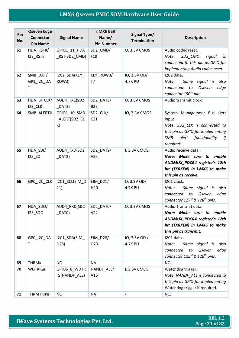
Table 5: 230-Pin PCB Edge Connector Pin Assignment
Pin
No.
Qseven Edge
Connector
Pin Name
Signal Name
i.MX6 Ball
Name/
Pin Number
Signal Type/
Termination Description
1 GND GND NA Power Ground.
2 GND GND NA Power Ground.
3 GBE_MDI3- GPHY_DTXRXM NA IO, DIFF Gigabit Ethernet MDI differential
pair 3 negative.
4 GBE_MDI2- GPHY_CTXRXM NA IO, DIFF Gigabit Ethernet MDI differential
pair 2 negative.
5 GBE_MDI3+ GPHY_DTXRXP NA IO, DIFF Gigabit Ethernet MDI differential
pair 3 positive.
6 GBE_MDI2+ GPHY_CTXRXP NA IO, DIFF Gigabit Ethernet MDI differential
pair 2 positive.
7 GBE_LINK10
0#
GPHY_LINK_LED
2
NA O, 3.3V CMOS 100Mbps Ethernet link status LED
Note: Same signal is also
connected to Qseven edge
connector 8th & 13th pins. So use
only in one place.
8 GBE_LINK10
00#
GPHY_LINK_LED
2
NA O, 3.3V CMOS Gigabit Ethernet link status LED
Note: Same signal is also
connected to Qseven edge
connector 7th & 13th pins. So use
only in one place.
9 GBE_MDI1- GPHY_BTXRXM NA IO, DIFF Gigabit Ethernet MDI differential
pair 1 negative.
10 GBE_MDI0- GPHY_ATXRXM NA IO, DIFF Gigabit Ethernet MDI differential
pair 0 negative.
11 GBE_MDI1+ GPHY_BTXRXP NA IO, DIFF Gigabit Ethernet MDI differential
pair 1 positive.
12 GBE_MDI0+ GPHY_ATXRXP NA IO, DIFF Gigabit Ethernet MDI differential
pair 0 positive.
13 GBE_LINK# GPHY_LINK_LED
2
NA O, 3.3V CMOS Gigabit Ethernet link status LED
Note: Same signal is also
connected to Qseven edge
connector 7th & 8th pins. So use
only in one place.
14 GBE_ACT# GPHY_ACTIVITY
_LED1
NA O, 3.3V CMOS Gigabit Ethernet activity status
LED.
15 GBE_CTREF NC NA - NC.

REL 1.2 Page 28 of 82
i.MX6 Qseven PMIC SOM Hardware User Guide
iWave Systems Technologies Pvt. Ltd.
Pin
No.
Qseven Edge
Connector
Pin Name
Signal Name
i.MX6 Ball
Name/
Pin Number
Signal Type/
Termination Description
16 SUS_S5# GPIO5_0_SUS_S
5(EIM_WAIT)¹
EIM_WAIT/
M25
O, 3.3V CMOS/
14.7K PD
S5 state is not supported.
EIM_WAIT is connected to this
pin for GPIO purpose through
resistor and default populated.
Note: Same signal is also
optionally connected to
Expansion connector2 40th pin
through resistor and default not
populated.
17 WAKE# GPIO6_10_WAK
E(NANDF_RB0)
NANDF_RB0/
B16
I, 3.3V CMOS External system wake event.
Note: NANDF_RB0 is connected to
this pin as GPIO for implementing
system wake event if required.
18 SUS_S3# NA NA O, 3.3V CMOS/
10K PU
S3 state is not supported.
Note: This pin is pulled up with
10K directly.
19 SUS_STAT# GPIO6_9_SUS_S
TAT(NANDF_WP
_B)
NANDF_WP_B/
E15
O, 3.3V CMOS Suspend status.
Note: NANDF_WP_B is connected
to this pin as GPIO for
implementing suspend status if
required.
20 PWRBTN# CPU_ON_OFF ONOFF/
D12
I, 3V CMOS Power button input.
Note: For more details on power
button usage, refer section 2.7.15
21 SLP_BTN# GPIO3_31_SLP_
BTN(EIM_D31)
EIM_D31/
H21
I, 3.3V CMOS Sleep button input.
Note: EIM_D31 is connected to
this pin as GPIO for implementing
sleep button functionality if
required.
22 LID_BTN# NC NA - NC.
23 GND GND NA Power Ground.
24 GND GND NA Power Ground.
25 GND GND NA Power Ground.
26 PWGIN PWRGIN NA I, 5V CMOS Active high enable signal for SOM
Power.
Note: For more details on
PWRGIN, refer Section 2.7.15.

REL 1.2 Page 29 of 82
i.MX6 Qseven PMIC SOM Hardware User Guide
iWave Systems Technologies Pvt. Ltd.
Pin
No.
Qseven Edge
Connector
Pin Name
Signal Name
i.MX6 Ball
Name/
Pin Number
Signal Type/
Termination Description
27 BATLOW# GPIO3_23_BATL
OW(EIM_D23)
EIM_D23/
D25
I, 3.3V CMOS Battery low input.
Note: EIM_D23 is connected to
this pin as GPIO for implementing
battery low functionality if
required.
28 RSTBTN# RSTBN NA I, 3V CMOS/
10K PU
Active low reset button input.
Note: This reset input is
connected to i.MX6 CPU’s POR
input.
29 SATA0_TX+ SATA_TXP SATA_TXP/
A12
O, DIFF/
0.01uF AC coupled
SATA0 transmit output
differential positive.
30 SATA1_TX+ NC NA - NC.
31 SATA0_TX- SATA_TXM SATA_TXM/
B12
O, DIFF/
0.01uF AC coupled
SATA0 transmit output
differential negative.
32 SATA1_TX- NC NA - NC.
33 SATA_ACT# GPIO4_10_SATA
_ACT(KEY_COL2
)
KEY_COL2/
W6
O, 3.3V OC SATA command activity line.
34 GND GND NA Power Ground.
35 SATA0_RX+ SATA_RXP SATA_RXP/
B14
I, DIFF/
0.01uF AC coupled
SATA0 receive input differential
positive.
36 SATA1_RX+ NC NA - NC.
37 SATA0_RX- SATA_RXM SATA_RXM/
A14
I, DIFF/
0.01uF AC coupled
SATA0 receive input differential
negative.
38 SATA1_RX- NC NA - NC.
39 GND GND NA Power Ground.
40 GND GND NA Power Ground.
41 BIOS_DISABL
E#/
BOOT_ALT#
NC NA - NC.
42 SDIO_CLK# SD1_CLK SD1_CLK/
D20
O, 3.3V CMOS SD1 clock.
43 SDIO_CD# GPIO7_0_SD1_C
D(SD3_DAT5)
SD3_DAT/
C13
I, 3.3V CMOS SD1 card detect.
Note: SD3_DAT5 is connected to
this pin as GPIO for implementing
SD/MMC card detect.
44 SDIO_LED GPIO6_7_SD1_L
ED(NANDF_CLE)
NANDF_CLE/
C15
O, 3.3V CMOS SD1 LED indication.
Note: NANDF_CLE is connected to
this pin as GPIO for implementing
SD/MMC LED indication.

REL 1.2 Page 30 of 82
i.MX6 Qseven PMIC SOM Hardware User Guide
iWave Systems Technologies Pvt. Ltd.
Pin
No.
Qseven Edge
Connector
Pin Name
Signal Name
i.MX6 Ball
Name/
Pin Number
Signal Type/
Termination Description
45 SDIO_CMD SD1_CMD SD1_CMD/
B21
IO, 3.3V CMOS SD1 command.
46 SDIO_WP GPIO6_11_SD1_
WP(NANDF_CS0
)
NANDF_CS0/
F15
I, 3.3V CMOS SD1 write Protect.
Note: NANDF_CS0 is connected to
this pin as GPIO for implementing
SD/MMC card write protect.
47 SDIO_PWR# GPIO6_14_SD1_
PWR(NANDF_CS
1)
NANDF_CS1/
C16
O, 3.3V CMOS SD1 card power enable.
Note: NANDF_CS1 is connected to
this pin as GPIO for implementing
SD/MMC card power enable.
48 SDIO_DAT1 SD1_DAT1 SD1_DAT1/
C20
IO, 3.3V CMOS SD1 data 1.
49 SDIO_DAT0 SD1_DAT0 SD1_DAT0/
A21
IO, 3.3V CMOS SD1 data 0.
50 SDIO_DAT3 SD1_DAT3 SD1_DAT3/
F18
IO, 3.3V CMOS SD1 data 3.
51 SDIO_DAT2 SD1_DAT2 SD1_DAT2/
E19
IO, 3.3V CMOS SD1 data 2.
52 SDIO_DAT5 SD1_DAT5(NAN
DF_D1)
NANDF_D1/
C17
IO, 3.3V CMOS SD1 data 5.
53 SDIO_DAT4 SD1_DAT4(NAN
DF_D0)
NANDF_D0/
A18
IO, 3.3V CMOS SD1 data 4.
54 SDIO_DAT7 SD1_DAT7(NAN
DF_D3)
NANDF_D3/
D17
IO, 3.3V CMOS SD1 data 7.
55 SDIO_DAT6 SD1_DAT6(NAN
DF_D2)
NANDF_D2/
F16
IO, 3.3V CMOS SD1 data 6.
56 RSVD GPIO3_22(EIM_
D22)
EIM_D22/
E23
IO, 3.3V CMOS Reserved.
EIM_D22 is connected to this pin
for GPIO purpose through resistor
and default populated.
57 GND GND NA Power Ground.
58 GND GND NA Power Ground.
59 HDA_SYNC/
I2S_WS
AUD4_TXFS(SD2
_DAT1)
SD2_DAT1/
E20
O, 3.3V CMOS Audio transmit frame
synchronization.
60 SMB_CLK/
GP1_I2C_CLK
I2C2_SCL(KEY_C
OL3)
KEY_COL3/
U5
O, 3.3V OD/
4.7K PU
I2C2 clock.
Note: Same signal is also
connected to Qseven edge
connector 152nd pin.
REL 1.2 Page 31 of 82
i.MX6 Qseven PMIC SOM Hardware User Guide
iWave Systems Technologies Pvt. Ltd.
Pin
No.
Qseven Edge
Connector
Pin Name
Signal Name
i.MX6 Ball
Name/
Pin Number
Signal Type/
Termination Description
61 HDA_RST#/
I2S_RST#
GPIO1_11_HDA
_RST(SD2_CMD)
SD2_CMD/
F19
O, 3.3V CMOS Audio codec reset.
Note: SD2_CMD signal is
connected to this pin as GPIO for
implementing Audio codec reset.
62 SMB_DAT/
GP1_I2C_DA
T
I2C2_SDA(KEY_
ROW3)
KEY_ROW3/
T7
IO, 3.3V OD/
4.7K PU
I2C2 data.
Note: Same signal is also
connected to Qseven edge
connector 150th pin.
63 HDA_BITCLK/
I2S_CLK
AUD4_TXC(SD2
_DAT3)
SD2_DAT3/
B22
O, 3.3V CMOS Audio transmit clock.
64 SMB_ALERT# GPIO1_10_SMB
_ALERT(SD2_CL
K)
SD2_CLK/
C21
IO, 3.3V CMOS System Management Bus alert
input.
Note: SD2_CLK is connected to
this pin as GPIO for implementing
SMB alert functionality if
required.
65 HDA_SDI/
I2S_SDI
AUD4_TXD(SD2
_DAT2)
SD2_DAT2/
A23
I, 3.3V CMOS Audio receive data.
Note: Make sure to enable
AUDMUX_PDCR4 register’s 12th
bit (TXRXEN) in i.MX6 to make
this pin as receive.
66 GP0_I2C_CLK I2C1_SCL(EIM_D
21)
EIM_D21/
H20
O, 3.3V OD/
4.7K PU
I2C1 clock.
Note: Same signal is also
connected to Qseven edge
connector 127th & 128th pins.
67 HDA_SDO/
I2S_SDO
AUD4_RXD(SD2
_DAT0)
SD2_DAT0/
A22
O, 3.3V CMOS Audio Transmit data.
Note: Make sure to enable
AUDMUX_PDCR4 register’s 12th
bit (TXRXEN) in i.MX6 to make
this pin as transmit.
68 GP0_I2C_DA
T
I2C1_SDA(EIM_
D28)
EIM_D28/
G23
IO, 3.3V OD /
4.7K PU
I2C1 data.
Note: Same signal is also
connected to Qseven edge
connector 125th & 126th pins.
69 THRM# NC NA - NC.
70 WDTRIG# GPIO6_8_WDTR
IG(NANDF_ALE)
NANDF_ALE/
A16
I, 3.3V CMOS Watchdog trigger.
Note: NANDF_ALE is connected to
this pin as GPIO for implementing
Watchdog trigger if required.
71 THRMTRIP# NC NA - NC.

REL 1.2 Page 32 of 82
i.MX6 Qseven PMIC SOM Hardware User Guide
iWave Systems Technologies Pvt. Ltd.
Pin
No.
Qseven Edge
Connector
Pin Name
Signal Name
i.MX6 Ball
Name/
Pin Number
Signal Type/
Termination Description
72 WDOUT WDOG_B(GPIO_
9)
NA O, 3.3V CMOS Watchdog event indicator.
Note: GPIO_9 is connected to this
pin through inverter.
Note: Same signal is optionally
connected to Expansion
connector1 8thpin (as ESAI_FSR)
through resistor and default not
populated.
73 GND GND NA Power Ground.
74 GND GND NA Power Ground.
75 USB_P7-/
USB_SSTX0-
NC NA - NC.
76 USB_P6-/
USB_SSRX0-
NC NA - NC.
77 USB_P7+/
USB_SSTX0+
NC NA - NC.
78 USB_P6+/
USB_SSRX0+
NC NA - NC.
79 USB_6_7_OC
#
NC NA - NC.
80 USB_4_5_OC
#
USB_4_5_OC NA I, 3.3V CMOS/
10K PU
Over current sense for USB port 4
& 5.
81 USB_P5-/
USB_SSTX1-
NC NA - NC.
82 USB_P4-/
USB_SSRX1-
USB_HUBP4_D
M
NA IO, DIFF USB Host port 4 data negative.
83 USB_P5+/
USB_SSTX1+
NC NA - NC.
84 USB_P4+/
USB_SSRX1+
USB_HUBP4_DP NA IO, DIFF USB Host port 4 data positive.
85 USB_2_3_OC
#
USB_2_3_OC NA I, 3.3V CMOS/
10K PU
Over current sense for USB port 2
& 3.
86 USB_0_1_OC
#
USB_0_1_OC NA I, 3.3V CMOS/
10K PU
Over current sense for USB port 0
& 1.
87 USB_P3- USB_HUBP3_D
M
NA IO, DIFF USB Host port 3 data negative.
88 USB_P2- USB_HUBP2_D
M
NA IO, DIFF USB Host port 2 data negative.
89 USB_P3+ USB_HUBP3_DP NA IO, DIFF USB Host port 3 data positive.
90 USB_P2+ USB_HUBP2_DP NA IO, DIFF USB Host port 2 data positive.

REL 1.2 Page 33 of 82
i.MX6 Qseven PMIC SOM Hardware User Guide
iWave Systems Technologies Pvt. Ltd.
Pin
No.
Qseven Edge
Connector
Pin Name
Signal Name
i.MX6 Ball
Name/
Pin Number
Signal Type/
Termination Description
91 USB_CC GPIO2_25_USB_
CC(EIM_OE)
EIM_OE/
J24
I, 3.3V CMOS USB client connect.
Note: EIM_OE is connected to this
pin as GPIO for implementing USB
client connect if required.
92 USB_ID USBOTG_ID(ENE
T_RX_ER)
ENET_RX_ER/
W23
I, 3.3V CMOS USB OTG ID to identify Host &
Device.
93 USB_P1- USB_OTG_DN USB_OTG_DN/
B6
IO, DIFF USB OTG data negative.
94 USB_P0- USB_HUBP1_D
M
NA IO, DIFF USB Host Port 1 data negative.
95 USB_P1+ USB_OTG_DP USB_OTG_DP/
A6
IO, DIFF USB OTG data positive.
96 USB_P0+ USB_HUBP1_DP NA IO, DIFF USB Host Port 1 data positive.
97 GND GND NA Power Ground.
98 GND GND NA Power Ground.
99 eDP0_TX0+/
LVDS_A0+
LVDS0_TX0_P LVDS0_TX0_P/
U1
O, 2.5V LVDS LVDS primary channel differential
pair 0 positive.
100 eDP1_TX0+/
LVDS_B0+
LVDS1_TX0_P LVDS1_TX0_P/
Y2
O, 2.5V LVDS LVDS secondary channel
differential pair 0 positive.
101 eDP0_TX0-/
LVDS_A0-
LVDS0_TX0_N LVDS0_TX0_N/
U2
O, 2.5V LVDS LVDS primary channel differential
pair 0 negative.
102 eDP1_TX0-/
LVDS_B0-
LVDS1_TX0_N LVDS1_TX0_N/
Y1
O, 2.5V LVDS LVDS secondary channel
differential pair 0 negative.
103 eDP0_TX1+/
LVDS_A1+
LVDS0_TX1_P LVDS0_TX1_P/
U3
O, 2.5V LVDS LVDS primary channel differential
pair 1 positive.
104 eDP1_TX1+/
LVDS_B1+
LVDS1_TX1_P LVDS1_TX1_P/
AA1
O, 2.5V LVDS LVDS secondary channel
differential pair 1 positive.
105 eDP0_TX1-/
LVDS_A1-
LVDS0_TX1_N LVDS0_TX1_N/
U4
O, 2.5V LVDS LVDS primary channel differential
pair 1 negative.
106 eDP1_TX1-/
LVDS_B1-
LVDS1_TX1_N LVDS1_TX1_N/
AA2
O, 2.5V LVDS LVDS secondary channel
differential pair 1 negative.
107 eDP0_TX2+/
LVDS_A2+
LVDS0_TX2_P LVDS0_TX2_P/
V1
O, 2.5V LVDS LVDS primary channel differential
pair2 positive.
108 eDP1_TX2+/
LVDS_B2+
LVDS1_TX2_P LVDS1_TX2_P/
AB2
O, 2.5V LVDS LVDS secondary channel
differential pair 2 positive.
109 eDP0_TX2-/
LVDS_A2-
LVDS0_TX2_N LVDS0_TX2_N/
V2
O, 2.5V LVDS LVDS primary channel differential
pair 2 negative.
110 eDP1_TX2-/
LVDS_B2-
LVDS1_TX2_N LVDS1_TX2_N/
AB1
O, 2.5V LVDS LVDS secondary channel
differential pair 2 negative.

REL 1.2 Page 34 of 82
i.MX6 Qseven PMIC SOM Hardware User Guide
iWave Systems Technologies Pvt. Ltd.
Pin
No.
Qseven Edge
Connector
Pin Name
Signal Name
i.MX6 Ball
Name/
Pin Number
Signal Type/
Termination Description
111 LVDS_PPEN GPIO2_4_LVDS_
PPEN(NANDF_D
4)
NANDF_D4/
A19
O, 3.3V CMOS Controls LVDS LCD panel power
enable.
Note: NANDF_D4 signal is
connected to this pin as GPIO for
implementing Panel power
enable.
112 LVDS_BLEN GPIO2_5_LVDS_
BLEN(NANDF_D
5)
NANDF_D5/
B18
O, 3.3V CMOS Controls LVDS LCD panel
backlight enable.
Note: NANDF_D5 is connected to
this pin as GPIO for implementing
backlight enable.
113 eDP0_TX3+/
LVDS_A3+
LVDS0_TX3_P LVDS0_TX3_P/
W1
O, 2.5V LVDS LVDS primary channel differential
pair 3 positive.
114 eDP1_TX3+/
LVDS_B3+
LVDS1_TX3_P LVDS1_TX3_P/
AA4
O, 2.5V LVDS LVDS secondary channel
differential pair 3 positive.
115 eDP0_TX3-/
LVDS_A3-
LVDS0_TX3_N LVDS0_TX3_N/
W2
O, 2.5V LVDS LVDS primary channel differential
pair 3 negative.
116 eDP1_TX3-/
LVDS_B3-
LVDS1_TX3_N LVDS1_TX3_N/
AA3
O, 2.5V LVDS LVDS secondary channel
differential pair 3 negative.
117 GND GND NA Power Ground.
118 GND GND NA Power Ground.
119 eDP0_AUX+/
LVDS_A_CLK
+
LVDS0_CLK_P LVDS0_CLK_P/
V3
O, 2.5V LVDS LVDS primary channel differential
clock positive.
120 eDP1_AUX+/
LVDS_B_CLK
+
LVDS1_CLK_P LVDS1_CLK_P/
Y4
O, 2.5V LVDS LVDS secondary channel
differential clock positive.
121 eDP0_AUX-/
LVDS_A_CLK-
LVDS0_CLK_N LVDS0_CLK_N/
V4
O, 2.5V LVDS LVDS primary channel differential
clock negative.
122 eDP1_AUX-/
LVDS_B_CLK-
LVDS1_CLK_N LVDS1_CLK_N/
Y3
O, 2.5V LVDS LVDS secondary channel
differential clock negative.
123 LVDS_BLT_C
TRL/GP_PW
M_OUT0
PWM2_PWMO(
GPIO_1)
GPIO_1/
T4
O, 3.3V CMOS LCD Panel backlight brightness
control via i.MX6 CPU’s PWM2.
Note: Same signal is optionally
connected to Qseven edge
connector 194th & 196th pins and
Expansion connector1 12th & 19th
pins through resistors and default
not populated.
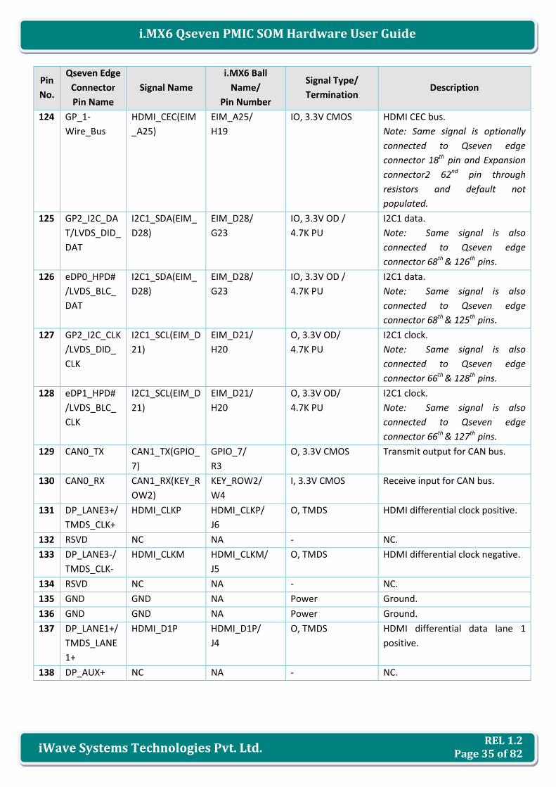
REL 1.2 Page 35 of 82
i.MX6 Qseven PMIC SOM Hardware User Guide
iWave Systems Technologies Pvt. Ltd.
Pin
No.
Qseven Edge
Connector
Pin Name
Signal Name
i.MX6 Ball
Name/
Pin Number
Signal Type/
Termination Description
124 GP_1-
Wire_Bus
HDMI_CEC(EIM
_A25)
EIM_A25/
H19
IO, 3.3V CMOS HDMI CEC bus.
Note: Same signal is optionally
connected to Qseven edge
connector 18th pin and Expansion
connector2 62nd pin through
resistors and default not
populated.
125 GP2_I2C_DA
T/LVDS_DID_
DAT
I2C1_SDA(EIM_
D28)
EIM_D28/
G23
IO, 3.3V OD /
4.7K PU
I2C1 data.
Note: Same signal is also
connected to Qseven edge
connector 68th & 126th pins.
126 eDP0_HPD#
/LVDS_BLC_
DAT
I2C1_SDA(EIM_
D28)
EIM_D28/
G23
IO, 3.3V OD /
4.7K PU
I2C1 data.
Note: Same signal is also
connected to Qseven edge
connector 68th & 125th pins.
127 GP2_I2C_CLK
/LVDS_DID_
CLK
I2C1_SCL(EIM_D
21)
EIM_D21/
H20
O, 3.3V OD/
4.7K PU
I2C1 clock.
Note: Same signal is also
connected to Qseven edge
connector 66th & 128th pins.
128 eDP1_HPD#
/LVDS_BLC_
CLK
I2C1_SCL(EIM_D
21)
EIM_D21/
H20
O, 3.3V OD/
4.7K PU
I2C1 clock.
Note: Same signal is also
connected to Qseven edge
connector 66th & 127th pins.
129 CAN0_TX CAN1_TX(GPIO_
7)
GPIO_7/
R3
O, 3.3V CMOS Transmit output for CAN bus.
130 CAN0_RX CAN1_RX(KEY_R
OW2)
KEY_ROW2/
W4
I, 3.3V CMOS Receive input for CAN bus.
131 DP_LANE3+/
TMDS_CLK+
HDMI_CLKP HDMI_CLKP/
J6
O, TMDS HDMI differential clock positive.
132 RSVD NC NA - NC.
133 DP_LANE3-/
TMDS_CLK-
HDMI_CLKM HDMI_CLKM/
J5
O, TMDS HDMI differential clock negative.
134 RSVD NC NA - NC.
135 GND GND NA Power Ground.
136 GND GND NA Power Ground.
137 DP_LANE1+/
TMDS_LANE
1+
HDMI_D1P HDMI_D1P/
J4
O, TMDS HDMI differential data lane 1
positive.
138 DP_AUX+ NC NA - NC.
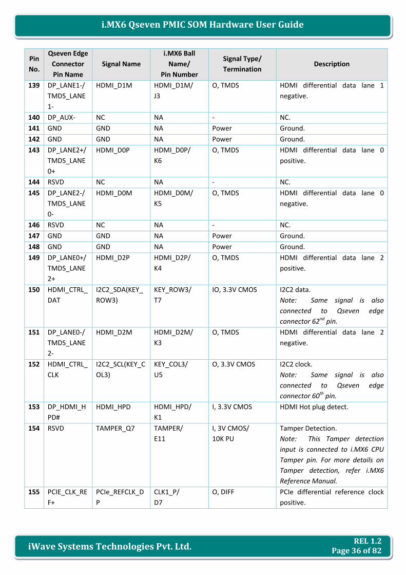
REL 1.2 Page 36 of 82
i.MX6 Qseven PMIC SOM Hardware User Guide
iWave Systems Technologies Pvt. Ltd.
Pin
No.
Qseven Edge
Connector
Pin Name
Signal Name
i.MX6 Ball
Name/
Pin Number
Signal Type/
Termination Description
139 DP_LANE1-/
TMDS_LANE
1-
HDMI_D1M HDMI_D1M/
J3
O, TMDS HDMI differential data lane 1
negative.
140 DP_AUX- NC NA - NC.
141 GND GND NA Power Ground.
142 GND GND NA Power Ground.
143 DP_LANE2+/
TMDS_LANE
0+
HDMI_D0P HDMI_D0P/
K6
O, TMDS HDMI differential data lane 0
positive.
144 RSVD NC NA - NC.
145 DP_LANE2-/
TMDS_LANE
0-
HDMI_D0M HDMI_D0M/
K5
O, TMDS HDMI differential data lane 0
negative.
146 RSVD NC NA - NC.
147 GND GND NA Power Ground.
148 GND GND NA Power Ground.
149 DP_LANE0+/
TMDS_LANE
2+
HDMI_D2P HDMI_D2P/
K4
O, TMDS HDMI differential data lane 2
positive.
150 HDMI_CTRL_
DAT
I2C2_SDA(KEY_
ROW3)
KEY_ROW3/
T7
IO, 3.3V CMOS I2C2 data.
Note: Same signal is also
connected to Qseven edge
connector 62nd pin.
151 DP_LANE0-/
TMDS_LANE
2-
HDMI_D2M HDMI_D2M/
K3
O, TMDS HDMI differential data lane 2
negative.
152 HDMI_CTRL_
CLK
I2C2_SCL(KEY_C
OL3)
KEY_COL3/
U5
O, 3.3V CMOS I2C2 clock.
Note: Same signal is also
connected to Qseven edge
connector 60th pin.
153 DP_HDMI_H
PD#
HDMI_HPD HDMI_HPD/
K1
I, 3.3V CMOS HDMI Hot plug detect.
154 RSVD TAMPER_Q7 TAMPER/
E11
I, 3V CMOS/
10K PU
Tamper Detection.
Note: This Tamper detection
input is connected to i.MX6 CPU
Tamper pin. For more details on
Tamper detection, refer i.MX6
Reference Manual.
155 PCIE_CLK_RE
F+
PCIe_REFCLK_D
P
CLK1_P/
D7
O, DIFF PCIe differential reference clock
positive.

REL 1.2 Page 37 of 82
i.MX6 Qseven PMIC SOM Hardware User Guide
iWave Systems Technologies Pvt. Ltd.
Pin
No.
Qseven Edge
Connector
Pin Name
Signal Name
i.MX6 Ball
Name/
Pin Number
Signal Type/
Termination Description
156 PCIE_WAKE# GPIO2_6_PCIe_
WAKE(NANDF_
D6)
NANDF_D6/
E17
I, 3.3V CMOS PCIe wake event.
Note: NANDF_D6 is connected to
this pin as GPIO for implementing
PCIe wake event if required.
157 PCIE_CLK_RE
F-
PCIe_REFCLK_D
N
CLK1_N/
C7
O, DIFF PCIe differential reference clock
negative.
158 PCIE_RST# GPIO2_7_PCIe_
RST(NANDF_D7)
SD4_DAT5/
C19
O, 3.3V CMOS PCIe reset.
Note: NANDF_D7 is connected to
this pin as GPIO for implementing
PCIe reset.
159 GND GND NA Power Ground.
160 GND GND NA Power Ground.
161 PCIE3_TX+ NC NA - NC.
162 PCIE3_RX+ NC NA - NC.
163 PCIE3_TX- NC NA - NC.
164 PCIE3_RX- NC NA - NC.
165 GND GND NA Power Ground.
166 GND GND NA Power Ground.
167 PCIE2_TX+ NC NA - NC.
168 PCIE2_RX+ NC NA - NC.
169 PCIE2_TX- NC NA - NC.
170 PCIE2_RX- NC NA - NC.
171 UART0_TX UART5_TXD(KEY
_COL1)
KEY_COL1/
U7
O, 3.3V CMOS UART5 serial data transmitter.
Note: Same signal is optionally
connected to Expansion
connector2 11th pin through
resistor and default not
populated.
172 UART0_RTS# UART5_CTS(KEY
_ROW4)
KEY_ROW4/
V5
O, 3.3V CMOS UART5 ready to receive data.
Note: Same signal is optionally
connected to Expansion
connector1 78th pin through
resistor and default not
populated.
173 PCIE1_TX+ NC NA - NC.
174 PCIE1_RX+ NC NA - NC.
175 PCIE1_TX- NC NA - NC.
176 PCIE1_RX- NC NA - NC.

REL 1.2 Page 38 of 82
i.MX6 Qseven PMIC SOM Hardware User Guide
iWave Systems Technologies Pvt. Ltd.
Pin
No.
Qseven Edge
Connector
Pin Name
Signal Name
i.MX6 Ball
Name/
Pin Number
Signal Type/
Termination Description
177 UART0_RX UART5_RXD(KEY
_ROW1)
KEY_ROW1/
U6
I, 3.3V CMOS UART5 serial data receiver.
Note: Same signal is optionally
connected to Expansion
connector2 07th pin through
resistor and default not
populated.
178 UART0_CTS# UART5_RTS(KEY
_COL4)
KEY_COL4/
T6
I, 3.3V CMOS UART5 ready to send data.
Note: Same signal is optionally
connected to Expansion
connector1 79th pin through
resistor and default not
populated.
179 PCIE0_TX+ PCIe_TXP PCIe_TXP/
B3
O, DIFF/
0.1uf AC coupled
PCIe differential transmit line
positive.
180 PCIE0_RX+ PCIe_RXP PCIe_RXP/
B2
O, DIFF PCIe differential receive line
positive
181 PCIE0_TX- PCIe_TXM PCIe_TXM/
A3
I, DIFF/
0.1uf AC coupled
PCIe differential transmit line
negative
182 PCIE0_RX- PCIe_RXM PCIe_RXM/
B1
I, DIFF PCIe differential receive line
negative
183 GND GND NA Power Ground.
184 GND GND NA Power Ground.
185 LPC_AD0/
GPIO0
GPIO1_8_Q7_G
PIO0(GPIO_8)
GPIO_8/
R5
IO, 3.3V CMOS General purpose input/output 0.
Note: Same signal is optionally
connected to Expansion
connector1 03rd pin through
resistor and default not
populated.
186 LPC_AD1/
GPIO1
GPIO7_11_Q7_
GPIO1(GPIO_16)
GPIO_16/
R2
IO, 3.3V CMOS General purpose input/output 1.
Note: Same signal is optionally
connected to Expansion
connector1 15th pin through
resistor and default not
populated.
187 LPC_AD2 /
GPIO2
GPIO7_12_Q7_
GPIO2(GPIO_17)
GPIO_17/
R1
IO, 3.3V CMOS General purpose input/output 2.
Note: Same signal is optionally
connected to Expansion
connector1 13th pin through
resistor and default not
populated.

REL 1.2 Page 39 of 82
i.MX6 Qseven PMIC SOM Hardware User Guide
iWave Systems Technologies Pvt. Ltd.
Pin
No.
Qseven Edge
Connector
Pin Name
Signal Name
i.MX6 Ball
Name/
Pin Number
Signal Type/
Termination Description
188 LPC_AD3/
GPIO3
GPIO7_13_Q7_
GPIO3(GPIO_18)
GPIO_18/
P6
IO, 3.3V CMOS General purpose input/output 3.
Note: Same signal is optionally
connected to Expansion
connector1 11th pin through
resistor and default not
populated.
189 LPC_CLK/
GPIO4
GPIO1_25_Q7_
GPIO4(ENET_CR
S_DV)
ENET_CRS_DV/
U21
IO, 3.3V CMOS General purpose input/output 4.
Note: Same signal is also
connected to Expansion
connector1 14th pin.
190 LPC_FRAME#
/ GPIO5
GPIO1_28_Q7_
GPIO5(ENET_TX
_EN)
ENET_TX_EN/
V21
IO, 3.3V CMOS General purpose input/output 5.
Note: Same signal is also
connected to Expansion
connector1 09th pin.
191 SERIRQ /
GPIO6
GPIO1_29_Q7_
GPIO6(ENET_TX
D1)
ENET_TX_D1/
W20
IO, 3.3V CMOS General purpose input/output 6.
Note: Same signal is also
connected to Expansion
connector1 07th pin.
192 LPC_LDRQ#/
GPIO7
GPIO1_30_Q7_
GPIO7(ENET_TX
D0)
ENET_TX_D0/
U20
IO, 3.3V CMOS General purpose input/output 7.
Note: Same signal is also
connected to Expansion
connector1 05th pin.
193 VCC_RTC VRTC_3V0 NA I, 3V Power 3V backup cell input for RTC.
194 SPKR/
GP_PWM_O
UT2
NC NA - Default NC.
Note: GPIO_1 is optionally
connected to this pin (for PWM2)
through resistor and default not
populated.
Note: Same signal is also
connected to Qseven edge
connector 123rd & 196th pins and
Expansion connector1 12th & 19th
pins through resistors.
195 FAN_TACHOI
N/
GP_TIMER_I
N
GPIO6_16_FAN
_CRTL(NANDF_
CS3)
NANDF_CS3/
D16
I, 3.3V CMOS Fan tachometer input.
Note: NANDF_CS3 is connected to
this pin as GPIO for implementing
Fan tachometer input if required.
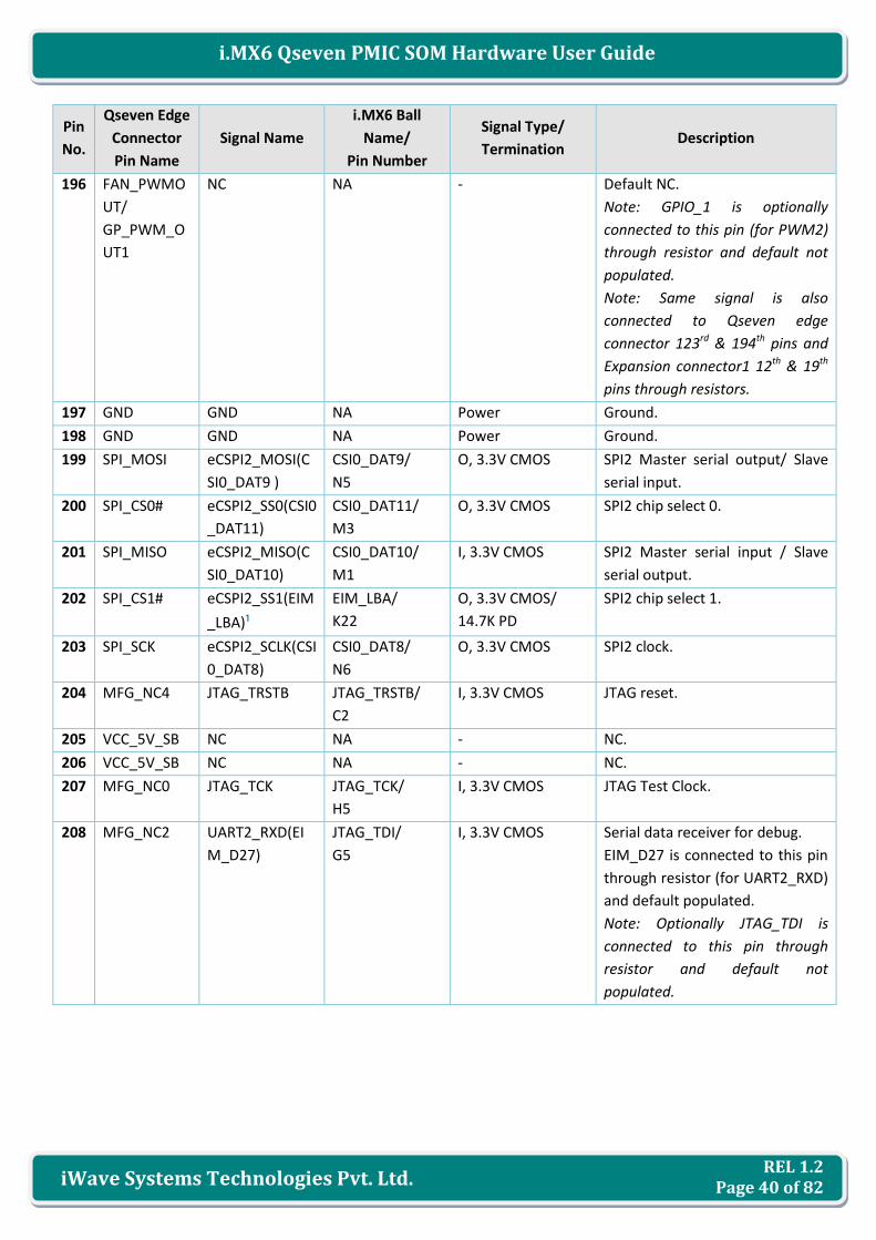
REL 1.2 Page 40 of 82
i.MX6 Qseven PMIC SOM Hardware User Guide
iWave Systems Technologies Pvt. Ltd.
Pin
No.
Qseven Edge
Connector
Pin Name
Signal Name
i.MX6 Ball
Name/
Pin Number
Signal Type/
Termination Description
196 FAN_PWMO
UT/
GP_PWM_O
UT1
NC NA - Default NC.
Note: GPIO_1 is optionally
connected to this pin (for PWM2)
through resistor and default not
populated.
Note: Same signal is also
connected to Qseven edge
connector 123rd & 194th pins and
Expansion connector1 12th & 19th
pins through resistors.
197 GND GND NA Power Ground.
198 GND GND NA Power Ground.
199 SPI_MOSI eCSPI2_MOSI(C
SI0_DAT9 )
CSI0_DAT9/
N5
O, 3.3V CMOS SPI2 Master serial output/ Slave
serial input.
200 SPI_CS0# eCSPI2_SS0(CSI0
_DAT11)
CSI0_DAT11/
M3
O, 3.3V CMOS SPI2 chip select 0.
201 SPI_MISO eCSPI2_MISO(C
SI0_DAT10)
CSI0_DAT10/
M1
I, 3.3V CMOS SPI2 Master serial input / Slave
serial output.
202 SPI_CS1# eCSPI2_SS1(EIM
_LBA)¹
EIM_LBA/
K22
O, 3.3V CMOS/
14.7K PD
SPI2 chip select 1.
203 SPI_SCK eCSPI2_SCLK(CSI
0_DAT8)
CSI0_DAT8/
N6
O, 3.3V CMOS SPI2 clock.
204 MFG_NC4 JTAG_TRSTB JTAG_TRSTB/
C2
I, 3.3V CMOS JTAG reset.
205 VCC_5V_SB NC NA - NC.
206 VCC_5V_SB NC NA - NC.
207 MFG_NC0 JTAG_TCK JTAG_TCK/
H5
I, 3.3V CMOS JTAG Test Clock.
208 MFG_NC2 UART2_RXD(EI
M_D27)
JTAG_TDI/
G5
I, 3.3V CMOS Serial data receiver for debug.
EIM_D27 is connected to this pin
through resistor (for UART2_RXD)
and default populated.
Note: Optionally JTAG_TDI is
connected to this pin through
resistor and default not
populated.

REL 1.2 Page 41 of 82
i.MX6 Qseven PMIC SOM Hardware User Guide
iWave Systems Technologies Pvt. Ltd.
Pin
No.
Qseven Edge
Connector
Pin Name
Signal Name
i.MX6 Ball
Name/
Pin Number
Signal Type/
Termination Description
209 MFG_NC1 UART2_TXD(EI
M_D26)
JTAG_TDO/
G6
O, 3.3V CMOS Serial data transmitter for debug.
EIM_D26 is connected to this pin
through resistor (for UART2_TXD)
and default populated.
Note: Optionally JTAG_TDO is
connected to this pin through
resistor and default not
populated.
210 MFG_NC3 JTAG_TMS JTAG_TMS/
C3
I, 3.3V CMOS JTAG Test Mode Select.
211 VCC VCC_5V NA I, 5V Power Supply Voltage.
212 VCC VCC_5V NA I, 5V Power Supply Voltage.
213 VCC VCC_5V NA I, 5V Power Supply Voltage.
214 VCC VCC_5V NA I, 5V Power Supply Voltage.
215 VCC VCC_5V NA I, 5V Power Supply Voltage.
216 VCC VCC_5V NA I, 5V Power Supply Voltage.
217 VCC VCC_5V NA I, 5V Power Supply Voltage.
218 VCC VCC_5V NA I, 5V Power Supply Voltage.
219 VCC VCC_5V NA I, 5V Power Supply Voltage.
220 VCC VCC_5V NA I, 5V Power Supply Voltage.
221 VCC VCC_5V NA I, 5V Power Supply Voltage.
222 VCC VCC_5V NA I, 5V Power Supply Voltage.
223 VCC VCC_5V NA I, 5V Power Supply Voltage.
224 VCC VCC_5V NA I, 5V Power Supply Voltage.
225 VCC VCC_5V NA I, 5V Power Supply Voltage.
226 VCC VCC_5V NA I, 5V Power Supply Voltage.
227 VCC VCC_5V NA I, 5V Power Supply Voltage.
228 VCC VCC_5V NA I, 5V Power Supply Voltage.
229 VCC VCC_5V NA I, 5V Power Supply Voltage.
230 VCC VCC_5V NA I, 5V Power Supply Voltage.
¹ Important Note: These signals are also used for i.MX6 CPU bootstrap setting on SOM and so no external loads or
pull-up/pull-down resistors to be connected to these pins which will change the boot configuration.
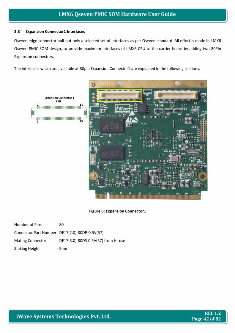
REL 1.2 Page 42 of 82
i.MX6 Qseven PMIC SOM Hardware User Guide
iWave Systems Technologies Pvt. Ltd.
2.8 Expansion Connector1 Interfaces
Qseven edge connector pull-out only a selected set of interfaces as per Qseven standard. All effort is made in i.MX6
Qseven PMIC SOM design, to provide maximum interfaces of i.MX6 CPU to the carrier board by adding two 80Pin
Expansion connectors.
The interfaces which are available at 80pin Expansion Connector1 are explained in the following sections.
Figure 6: Expansion Connector1
Number of Pins - 80
Connector Part Number - DF17(2.0)-80DP-0.5V(57)
Mating Connector - DF17(3.0)-80DS-0.5V(57) from Hirose
Staking Height - 5mm

REL 1.2 Page 43 of 82
i.MX6 Qseven PMIC SOM Hardware User Guide
iWave Systems Technologies Pvt. Ltd.
2.8.1 Parallel LCD Display Interface
i.MX6 Qseven PMIC SOM supports one Parallel RGB display interface and MIPI DSI interface on Expansion
connector1 along with two LVDS display & one HDMI display on Qseven Edge connector. i.MX6 CPU’s IPU is used for
parallel LCD display interface which supports upto 24bit data bus (8bits/colour). i.MX6 CPU’s LCD can support data
rate up to 220 Mpixels/sec (e.g. WUXGA+@ 60Hz).
For more details, refer Expansion connector1 pins 2,4,6 & 20 to 47 on Table 6 and Expansion connector2 pins
41,43,44 & 45 on Table 7.
Note: i.MX6 Duallite and i.MX6 Solo CPU supports only one IPU and so at any time only two display interfaces
(including LVDS, HDMI & MIPI DSI) can be supported.
2.8.2 MIPI DSI Interface
i.MX6 Qseven PMIC SOM supports dual lane MIPI DSI interface (excluding clock lane) @ 1Gbps on Expansion
connector1. i.MX6 CPU’s IPU with MIPI DSI Host controller & MIPI D-PHY is used for MIPI DSI interface. It is
compliant with MIPI Alliance Specification for Display Serial Interface (DSI), Version 1.01.00 - 21 February 2008 with
DPI-2 & DBI-2 support. It supports programmable display resolutions from 160x120(QQVGA) to 1280x720(XVGA). It
supports different Video Mode Pixel Formats, 16 bpp(RGB565), 18 bpp(RGB666) packed, 18 bpp(RGB666) loosely &
24 bpp(RGB888).
For more details, refer Expansion connector1 pins 46,48,55,56,57 & 58 on Table 6.
Note: i.MX6 Duallite and i.MX6 Solo CPU supports only one IPU and so at any time only two display interfaces
(including LVDS, HDMI & MIPI DSI) can be supported.
2.8.3 Parallel Camera Interface1
i.MX6 Qseven PMIC SOM supports one camera interface on Expansion connector1 along with one more camera
interface & MIPI CSI interface on Expansion connector2. i.MX6 QuadPlus/Quad/DualPlus/Dual CPU has two IPU block
and each IPU has two input ports CSI0 and CSI1 which can receive data concurrently and independently. At any given
time, an IPU input port may receive data either from a parallel external port or from the MIPI/CSI-2 receiver.
i.MX6 IPU’s CSI0 parallel port is used for camera1 interface which provides direct connectivity to most relevant
image sensors and to TV decoders. The sensor is the master of the pixel clock (PIXCLK) & synchronization signals
where synchronization signals can be received using dedicated control signals method (HSYNC & VSYNC) or controls
embedded in data stream method (BT.656 protocol). i.MX6 Qseven PMIC SOM supports 8bit camera interface.
For more details, refer Expansion connector1 pins 64 to 76 on Table 6.
Note: i.MX6 Duallite and i.MX6 Solo CPU supports only one IPU.

REL 1.2 Page 44 of 82
i.MX6 Qseven PMIC SOM Hardware User Guide
iWave Systems Technologies Pvt. Ltd.
2.8.4 ESAI Interface
i.MX6 Qseven PMIC SOM supports one ESAI interface on Expansion connector1. i.MX6 CPU’s ESAI module is used for
ESAI interface which provides a full-duplex serial port for serial communication with a variety of serial devices,
including industry-standard codecs, SPDIF transceivers and other DSPs. The ESAI features independent
(asynchronous mode) or shared (synchronous mode) transmit and receive sections with separate or shared
internal/external clocks and frame syncs operating in Master or Slave mode.
It supports up to six transmitters and four receivers with TX2_RX3, TX3_RX2, TX4_RX1, and TX5_RX0 pins shared by
transmitters 2 to 5 and receivers 0 to 3. TX0 and TX1 pins are used by transmitters 0 and 1 only. It has 128-word
Transmit FIFO shared by six transmitters and 128-word Receive FIFO shared by four receivers. It also supports
programmable data interface modes (such as I2S, LSB aligned, MSB aligned) and programmable word length (8, 12,
16, 20 or 24bits).
For more details, refer Expansion connector1 pins 3,5,7 to 14, 16 & 18 on Table 6.
2.8.5 SPDIF Interface
i.MX6 Qseven PMIC SOM supports one SPDIF interface on Expansion connector1. i.MX6 CPU’s SPDIF module is used
for SPDIF interface which is a stereo transceiver that allows the processor to receive and transmit digital audio over
it using the IEC60958 standard. It is composed of SPDIF Receiver with one input & SPDIF Transmitter with one output
and allows the handling of both SPDIF channel status (CS) and User (U) data.
The SPDIF receiver extracts the audio data from each SPDIF frame and places the data in the SPDIF Rx left and right
FIFOs. The SPDIF transmitter generates a SPDIF output bit stream in the biphase mark format (IEC60958), which
consists of audio data, channel status and user bits.
For more details, refer Expansion connector1 pins 15 & 17 on Table 6.
2.8.6 Data UART Interface (UART1 & UART3)
i.MX6 Qseven PMIC SOM supports two Data UART interface on Expansion connector1 along with one more on
Qseven Edge connector and one more on Expansion connector2. i.MX6 CPU’s UART1 and UART3 controller is used
for Data UART interface on Expansion connector1 which supports Serial RS-232NRZ mode, 9-bit RS-485 mode and
IrDA mode. It is compatible with High-speed TIA/EIA-232-F (up to 5.0 Mbit/s) with auto baud rate detection (up to
115.2 Kbit/s). It supports 7 or 8 data bits for RS-232 characters (9 bit RS-485 format), 1 or 2 stop bits and
programmable parity (even, odd, and no parity). Also i.MX6 Qseven PMIC SOM supports hardware flow control for
request to send and clear to send signals.
For more details, refer Qseven Edge connector pins 51 to 54 & 61 to 64 on Table 6.

REL 1.2 Page 45 of 82
i.MX6 Qseven PMIC SOM Hardware User Guide
iWave Systems Technologies Pvt. Ltd.
Table 6: Expansion Connector1 Pin Assignment
Pin
No Signal Name
i.MX6
Ball Name/
Pin Number
Signal Type/
Termination Description
1 GND NA Power Ground.
2 DISP0_DAT23 DISP0_DAT23/
W24
O, 3.3V CMOS Parallel LCD data 23 (Red data 7).
3 NC NA - Default NC.
Note: GPIO_8 is optionally connected
to this pin (for ESAI_TX5_RX0) through
resistor and default not populated.
Note: Same signal is connected to
Qseven edge connector 185th pin
through resistor and default
populated.
4 DISP0_DAT22 DISP0_DAT22/
V24
O, 3.3V CMOS Parallel LCD data 22 (Red data 6).
5 ESAI_TX4_RX1(ENET_TXD0) ENET_TXD0/
U20
IO, 3.3V CMOS ESAI Serial Transmit4/Receive1 Data.
Note: Same signal is also connected to
Qseven edge connector 192nd pin.
6 DISP0_DAT18 DISP0_DAT18/
V25
O, 3.3V CMOS Parallel LCD data 18 (Red data 2).
7 ESAI_TX2_RX3(ENET_TXD1) ENET_TXD1/
W20
IO, 3.3V CMOS ESAI Serial Transmit2/Receive3 Data.
Note: Same signal is also connected to
Qseven edge connector 191st pin.
8 NC NA - Default NC.
Note: GPIO_9 is optionally connected
to this pin (for ESAI_FSR) through
resistor and default not populated.
Note: Same signal is also connected to
Qseven edge connector 72nd pin
through resistor option and default
populated.
9 ESAI_TX3_RX2(ENET_TX_EN) ENET_TX_EN/
V21
IO, 3.3V CMOS ESAI Serial Transmit3/Receive2 Data.
Note: Same signal is also connected to
Qseven edge connector 190th pin.
10 NC NA - Default NC.
Note: GPIO_3 is optionally connected
to this pin (for ESAI_HCKR) through
resistor and default not populated.
Note: Same signal is also connected to
Expansion connector2 2nd pin using
resistor and default populated.

REL 1.2 Page 46 of 82
i.MX6 Qseven PMIC SOM Hardware User Guide
iWave Systems Technologies Pvt. Ltd.
Pin
No Signal Name
i.MX6
Ball Name/
Pin Number
Signal Type/
Termination Description
11 NC NA - Default NC.
Note: GPIO_18 is optionally connected
to this pin (for ESAI_TX1) through
resistor and default not populated.
Note: Same signal is connected to
Qseven edge connector 188th pin
through resistor and default
populated.
12 NC NA - Default NC.
Note: GPIO_1 is optionally connected
to this pin (for ESAI_RX_CLK) through
resistor and default not populated.
Note: Same signal is connected to
Qseven edge connector 123rd, 194th &
196th pins and Expansion connector1
19th Pin through resistors.
13 NC NA - Default NC.
Note: GPIO_17 is optionally connected
to this pin (for ESAI_TX0) through
resistor and default not populated.
Note: Same signal is connected to
Qseven edge connector 187th pin
through resistor and default
populated.
14 ESAI_SCKT(ENET_CRS_DV) ENET_CRS_DV
/U21
IO, 3.3V CMOS ESAI Transmitter Serial Clock.
Note: Same signal is also connected to
Qseven edge connector 189th pin.
15 NC NA - Default NC.
Note: GPIO_16 is optionally connected
to this pin (for SPDIF_IN1) through
resistor and default not populated.
Note: Same signal is connected to
Qseven edge connector 186th pin
through resistor and default
populated.
16 ESAI_FST(ENET_RXD1) ENET_RXD1/
W22
IO, 3.3V CMOS/
10K PU/PD¹
ESAI Frame Sync for Transmitter.
17 SPDIF_OUT1(GPIO_19) GPIO_19/
P5
O, 3.3V CMOS SPDIF output line.
18 ESAI_HCKT(ENET_RXD0) ENET_RXD0/
W21
IO, 3.3V CMOS/
10K PU/PD¹
ESAI High Frequency Clock for
Transmitter.

REL 1.2 Page 47 of 82
i.MX6 Qseven PMIC SOM Hardware User Guide
iWave Systems Technologies Pvt. Ltd.
Pin
No Signal Name
i.MX6
Ball Name/
Pin Number
Signal Type/
Termination Description
19 NC NA - Default NC.
Note: GPIO_1 is optionally connected
to this pin (for PWM2) through resistor
and default not populated.
Note: Same signal is connected to
Qseven edge connector 123rd, 194th &
196th pins and Expansion connector1
12th Pin through resistors.
20 DISP0_DAT17 DISP0_DAT17/
U24
O, 3.3V CMOS Parallel LCD data 17 (Red data1).
21 DISP0_DAT14 DISP0_DAT14/
U25
O, 3.3V CMOS Parallel LCD data 14 (Green data6).
22 DISP0_DAT12 DISP0_DAT12/
T24
O, 3.3V CMOS Parallel LCD data 12(Green data4).
23 DISP0_DAT9 DISP0_DAT9/
T25
O, 3.3V CMOS Parallel LCD data 9 (Green data1).
24 DISP0_DAT7 DISP0_DAT7/
R24
O, 3.3V CMOS Parallel LCD data 7 (Blue data7).
25 DISP0_DAT5 DISP0_DAT5/
R25
O, 3.3V CMOS Parallel LCD data 5 (Blue data5).
26 DISP0_DAT0 DISP0_DAT0/
P24
O, 3.3V CMOS/
10K PU/PD¹
Parallel LCD data 0 (Blue data0).
27 GND NA Power Ground.
28 DISP0_DAT3 DISP0_DAT3/
P21
O, 3.3V CMOS Parallel LCD data 3 (Blue data 3).
29 DISP0_DAT10 DISP0_DAT10/
R21
O, 3.3V CMOS Parallel LCD data 10 (Green data2).
30 DISP0_DAT4 DISP0_DAT4/
P20
O, 3.3V CMOS Parallel LCD data 4 (Blue data 4).
31 DISP0_DAT13 DISP0_DAT13/
R20
O, 3.3V CMOS Parallel LCD data 13 (Green data5).
32 GND NA Power Ground.
33 DISP0_DAT21 DISP0_DAT21/
T20
O, 3.3V CMOS Parallel LCD data 21 (Red data5).
34 DISP0_DAT16 DISP0_DAT16/
T21
O, 3.3V CMOS Parallel LCD data 16 (Red data0).
35 DISP0_DAT20 DISP0_DAT20/
U22
O, 3.3V CMOS Parallel LCD data 20 (Red data4).
36 DISP0_DAT19 DISP0_DAT19/
U23
O, 3.3V CMOS Parallel LCD data 19 (Red data3).
37 GND NA Power Ground.
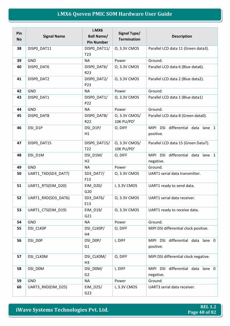
REL 1.2 Page 48 of 82
i.MX6 Qseven PMIC SOM Hardware User Guide
iWave Systems Technologies Pvt. Ltd.
Pin
No Signal Name
i.MX6
Ball Name/
Pin Number
Signal Type/
Termination Description
38 DISP0_DAT11 DISP0_DAT11/
T23
O, 3.3V CMOS Parallel LCD data 11 (Green data3).
39 GND NA Power Ground.
40 DISP0_DAT6 DISP0_DAT6/
R23
O, 3.3V CMOS Parallel LCD data 6 (Blue data6).
41 DISP0_DAT2 DISP0_DAT2/
P23
O, 3.3V CMOS Parallel LCD data 2 (Blue data2).
42 GND NA Power Ground.
43 DISP0_DAT1 DISP0_DAT1/
P22
O, 3.3V CMOS Parallel LCD data 1 (Blue data1)
44 GND NA Power Ground.
45 DISP0_DAT8 DISP0_DAT8/
R22
O, 3.3V CMOS/
10K PU/PD¹
Parallel LCD data 8 (Green data0).
46 DSI_D1P DSI_D1P/
H1
O, DIFF MIPI DSI differential data lane 1
positive.
47 DISP0_DAT15 DISP0_DAT15/
T22
O, 3.3V CMOS/
10K PU/PD¹
Parallel LCD data 15 (Green Data7).
48 DSI_D1M DSI_D1M/
H2
O, DIFF MIPI DSI differential data lane 1
negative.
49 GND NA Power Ground.
50 UART1_TXD(SD3_DAT7) SD3_DAT7/
F13
O, 3.3V CMOS UART1 serial data transmitter.
51 UART1_RTS(EIM_D20) EIM_D20/
G20
I, 3.3V CMOS UART1 ready to send data.
52 UART1_RXD(SD3_DAT6) SD3_DAT6/
E13
O, 3.3V CMOS UART1 serial data receiver.
53 UART1_CTS(EIM_D19) EIM_D19/
G21
O, 3.3V CMOS UART1 ready to receive data.
54 GND NA Power Ground.
55 DSI_CLK0P DSI_CLK0P/
H4
O, DIFF MIPI DSI differential clock positive.
56 DSI_D0P DSI_D0P/
G1
I, DIFF MIPI DSI differential data lane 0
positive.
57 DSI_CLK0M DSI_CLK0M/
H3
O, DIFF MIPI DSI differential clock negative.
58 DSI_D0M DSI_D0M/
G2
I, DIFF MIPI DSI differential data lane 0
negative.
59 GND NA Power Ground.
60 UART3_RXD(EIM_D25) EIM_D25/
G22
I, 3.3V CMOS UART3 serial data receiver.

REL 1.2 Page 49 of 82
i.MX6 Qseven PMIC SOM Hardware User Guide
iWave Systems Technologies Pvt. Ltd.
Pin
No Signal Name
i.MX6
Ball Name/
Pin Number
Signal Type/
Termination Description
61 UART3_RTS(SD3_RST) SD3_RST/
D15
I, 3.3V CMOS UART3 ready to send data.
62 UART3_CTS(EIM_D30) EIM_D30/
J20
O, 3.3V CMOS UART3 ready to receive data.
63 UART3_TXD(EIM_D24) EIM_D24/
F22
O, 3.3V CMOS UART3 serial data transmitter.
64 CLKO(GPIO_0) GPIO_0/
T5
O, 3.3V CMOS General purpose configurable clock
from CPU.
Note: This clock output can be used as
Master clock input to parallel camera.
65 CSI0_PIXCLK CSI0_PIXCLK/
P1
I, 3.3V CMOS Parallel camera 0 PIXCLK.
66 CSI0_HSYNC CSI0_MCLK/
P4
I, 3.3V CMOS Parallel camera 0 HSYNC.
67 CSI0_DATA_EN CSI0_DATA_E
N/
P3
I, 3.3V CMOS Parallel camera 0 data enable.
68 CSI0_VSYNC CSI0_VSYNC/
N2
I, 3.3V CMOS Parallel camera 0 VSYNC.
69 CSI0_DAT12 CSI0_DAT12/
M2
I, 3.3V CMOS Parallel camera 0 data 0.
70 CSI0_DAT13 CSI0_DAT13/
L1
I, 3.3V CMOS Parallel camera 0 data 1.
71 CSI0_DAT14 CSI0_DAT14/
M4
I, 3.3V CMOS Parallel camera 0 data 2.
72 CSI0_DAT15 CSI0_DAT15/
M5
I, 3.3V CMOS Parallel camera 0 data 3.
73 CSI0_DAT16 CSI0_DAT16/
L4
I, 3.3V CMOS Parallel camera 0 data 4.
74 CSI0_DAT18 CSI0_DAT18/
M6
I, 3.3V CMOS Parallel camera 0 data 6.
75 CSI0_DAT19 CSI0_DAT19/
L6
I, 3.3V CMOS Parallel camera 0 data 7.
76 CSI0_DAT17 CSI0_DAT17/
L3
I, 3.3V CMOS Parallel camera 0 data 5.
77 DI0_DISP_CLK DI0_DISP_CLK/
N19
O, 3.3V CMOS Parallel LCD clock.

REL 1.2 Page 50 of 82
i.MX6 Qseven PMIC SOM Hardware User Guide
iWave Systems Technologies Pvt. Ltd.
Pin
No Signal Name
i.MX6
Ball Name/
Pin Number
Signal Type/
Termination Description
78 NC NA - Default NC.
Note: KEY_ROW4 is optionally
connected to this pin (for CAN2_RX)
through resistor and default not
populated.
Note: Same signal is connected to
Qseven edge connector 172nd Pin
through resistor and default
populated.
79 NC NA - Default NC.
Note: KEY_COL4 is optionally
connected to this pin (for CAN2_TX)
through resistor and default not
populated.
Note: Same signal is connected to
Qseven edge connector 178th Pin
through resistor and default
populated.
80 GND NA Power Ground.
¹ Note: These signals are also used internally On-SOM for setting SOM configuration and so Pull-up or Pull down on
pins will vary depend upon SOM configuration.

REL 1.2 Page 51 of 82
i.MX6 Qseven PMIC SOM Hardware User Guide
iWave Systems Technologies Pvt. Ltd.
2.9 Expansion Connector2 Interfaces
i.MX6 Qseven PMIC SOM supports Expansion connector2 also to pull out more interfaces of i.MX6 CPU to carrier
board. The interfaces which are available at 80pin Expansion connector2 are listed in the following sections.
Figure 7: Expansion Connector1
Number of Pins - 80
Connector Part Number - DF17(2.0)-80DP-0.5V(57)
Mating Connector - DF17(3.0)-80DS-0.5V(57) from Hirose
Staking Height - 5mm
REL 1.2 Page 52 of 82
i.MX6 Qseven PMIC SOM Hardware User Guide
iWave Systems Technologies Pvt. Ltd.
2.9.1 Parallel Camera Interface2
i.MX6 Qseven PMIC SOM supports one camera interface along with MIPI CSI interface on Expansion connector2 and
one more camera interface on Expansion connector1. i.MX6 QuadPlus/Quad/DualPlus/Dual CPU has two IPU block
and each IPU has two input ports CSI0 and CSI1 which can receive data concurrently and independently. At any given
time, an IPU input port may receive data either from a parallel external port or from the MIPI/CSI-2 receiver.
i.MX6 IPU’s CSI1 parallel port is used for camera2 interface which provides direct connectivity to most relevant
image sensors and to TV decoders. The sensor is the master of the pixel clock (PIXCLK) & synchronization signals
where synchronization signals can be received using dedicated control signals method (HSYNC & VSYNC) or controls
embedded in data stream method (BT.656 protocol). i.MX6 Qseven PMIC SOM supports 8bit camera interface.
For more details, refer Expansion connector2 pins 48 to 58 on Table 7.
Note: i.MX6 Duallite and i.MX6 Solo CPU supports only one IPU.
2.9.2 MIPI CSI Interface
i.MX6 Qseven PMIC SOM supports four data lane MIPI CSI interface (excluding clock lane) from 80 Mbps up to 1
Gbps speed per data lane on Expansion connector2. i.MX6 QuadPlus/Quad/DualPlus/Dual CPU has two IPU block
and each IPU has two input ports CSI0 and CSI1 which can receive data concurrently and independently. At any given
time, an IPU input port may receive data either from a parallel external port or from the MIPI/CSI-2 receiver.
The MIPI/CSI-2 port can receive up to 4 concurrent data channels. Each data channel is routed to a different CSI
input of the IPU (2 IPUs, 2 CSIs on each IPU; a total of 4 CSI inputs). Pixel data can be further processed by the IPU.
Other data types can be transferred through a CSI transparently as generic data to the system memory.
i.MX6 CPU’s IPU with MIPI CSI-2 Host controller & MIPI D-PHY is used for MIPI CSI interface. It is compliant with MIPI
Alliance Standard for Camera Serial Interface 2 (CSI-2) Version 1.00 and Interface with MIPI D-PHY following PHY
Protocol Interface (PPI) as defined in MIPI Alliance Specification for D-PHY Version 1.00. It supports all primary and
secondary data formats with RGB, YUV and RAW colour space definitions from 24-bit down to 6-bit per pixel.
For more details, refer Expansion connector2 pins 61,63,65,67,69,71,73.75,79 & 80 on Table 7.
Note: i.MX6 Duallite and i.MX6 Solo CPU supports only one IPU and so only two MIPI CSI data lane is supported.

REL 1.2 Page 53 of 82
i.MX6 Qseven PMIC SOM Hardware User Guide
iWave Systems Technologies Pvt. Ltd.
2.9.3 Memory Bus Interface
i.MX6 Qseven PMIC SOM supports one memory interface on Expansion connector2. i.MX6 CPU’s EIM module is used
for Memory interface which handles the interface to devices external to the chip including generation of chip selects,
clock and control for external peripherals and memory. i.MX6 Qseven PMIC SOM supports multiplexed address /
data bus with x8 , x16 port size. This multiplexing addresses and data bits on the same pins is supported for
synchronous/asynchronous accesses to x8/x16 data width memory devices.
For more details, refer Expansion connector2 pins 17 to 40 & 42 on Table 7.
2.9.4 Keypad Interface
i.MX6 Qseven PMIC SOM supports 3x3 Keypad interface on Expansion connector2. i.MX6 CPU’s Keypad port is used
for Keypad interface which provides interface for the keypad matrix with 2-point contact or 3-point contact keys.
With appropriate software support, the KPP is capable of detecting, debouncing, and decoding one or multiple keys
pressed simultaneously on the keypad. It also supports Long key-press detection & Standby key-press detection with
Glitch suppression.
For more details, refer Expansion connector2 pins 7 to 14 on Table 7.
2.9.5 Data UART Interface (UART4)
i.MX6 Qseven PMIC SOM supports one Data UART interface on Expansion connector2 along with one more on
Qseven Edge connector and two more on Expansion connector1. i.MX6 CPU’s UART4 controller is used for Data
UART interface on Expansion connector2 which supports Serial RS-232NRZ mode, 9-bit RS-485 mode and IrDA mode.
It is compatible with High-speed TIA/EIA-232-F (up to 5.0 Mbit/s) with auto baud rate detection (up to 115.2 Kbit/s).
It supports 7 or 8 data bits for RS-232 characters (9 bit RS-485 format), 1 or 2 stop bits and programmable parity
(even, odd, and no parity).
For more details, refer Expansion connector2 pins 64 & 68 on Table 7.
2.9.6 MLB Interface
i.MX6 Qseven PMIC SOM supports MLB interface on Expansion connector2. i.MX6 CPU’s MLB module is used for
MLB interface which provides interface to MOST Networks (MOST25,MOST50,MOST150) and implemented with
an MediaLB 3-pin interface. This is capable of exchanging data at speeds up to 1024xFs.
For more details, refer Expansion connector2 pins 1,2 & 4 on Table 7.
Note: MLB is supported only in automotive grade i.MX6 CPUs.

REL 1.2 Page 54 of 82
i.MX6 Qseven PMIC SOM Hardware User Guide
iWave Systems Technologies Pvt. Ltd.
Table 7: Expansion Connector2 Pin Assignment
Pin
No Signal Name
i.MX6 Ball
Name/
Pin Number
Signal Type/
Termination Description
1 MLBDAT(GPIO_2) GPIO_2/
T1
IO,3.3V CMOS MLB single ended data.
Note: MLB differential data negative
(MLB_DN) is optionally connected to
this pin through resistor and default
not populated.
2 MLBCLK(GPIO_3) GPIO_3/
R7
I,3.3V CMOS MLB single ended clock.
Note: Optionally same signal is
connected to Expansion connector1
10th pin (for ESAI_HCKR) through
resistor and default not populated.
Note: MLB differential clock positive
(MLB_CP) is optionally connected to
this pin through resistor and default
not populated.
3 NC NA - Default NC.
Note: MLB differential data positive
(MLB_DP) is optionally connected to
this pin through resistor and default
not populated.
4 MLBSIG(GPIO_6) GPIO_6/
T3
I, 3.3V CMOS MLB single ended signal.
Note: MLB differential clock negative
(MLB_CN) is optionally connected to
this pin through resistor and default
not populated.
5 GND NA Power Ground.
6 GND NA Power Ground.
7 NC NA - Default NC.
Note: KEY_ROW1 is optionally
connected to this pin (for KEY_ROW1)
through resistor and default not
populated.
Note: Same signal is connected to
Qseven edge connector 177th Pin
through resistor and default
populated.
8 KEY_ROW5(CSI0_DAT5) CSI0_DAT5/
P2
O, 3.3V CMOS Keypad row 5.
9 KEY_ROW6(CSI0_DAT7) CSI0_DAT7/
N3
O, 3.3V CMOS Keypad row 6.

REL 1.2 Page 55 of 82
i.MX6 Qseven PMIC SOM Hardware User Guide
iWave Systems Technologies Pvt. Ltd.
Pin
No Signal Name
i.MX6 Ball
Name/
Pin Number
Signal Type/
Termination Description
10 KEY_ROW7(GPIO_5) GPIO_5/
R4
O, 3.3V CMOS Keypad row 7.
11 NC NA - Default NC.
Note: KEY_COL1 is optionally
connected to this pin (for KEY_COL1)
through resistor and default not
populated.
Note: Same signal is connected to
Qseven edge connector 171st Pin
through resistor and default
populated.
12 KEY_COL5(CSI0_DAT4) CSI0_DAT4/
N1
I, 3.3V CMOS Keypad column 5.
13 KEY_COL6(CSI0_DAT6) CSI0_DAT6/
N4
I, 3.3V CMOS Keypad column 6.
14 KEY_COL7(GPIO_4) GPIO_4/
R6
I, 3.3V CMOS Keypad column 7.
15 GND NA Power Ground.
16 GND NA Power Ground.
17 EIM_DA1¹ EIM_DA1/
J25
IO, 3.3V CMOS/
14.7K PD²
EIM data & address line 1.
18 EIM_DA0¹ EIM_DA0/
L20
IO, 3.3V CMOS/
14.7K PD
EIM data & address line 0.
19 EIM_DA3¹ EIM_DA3/
K24
IO, 3.3V CMOS/
14.7K PD
EIM data & address line 3.
20 EIM_DA2¹ EIM_DA2/
L21
IO, 3.3V CMOS/
14.7K PD
EIM data & address line 2.
21 EIM_DA5¹ EIM_DA5/
L23
IO, 3.3V CMOS/
4.7K PU²
EIM data & address line 5.
22 EIM_DA4¹ EIM_DA4/
L22
IO, 3.3V CMOS/
4.7K PU²
EIM data & address line 4.
23 EIM_DA7¹ EIM_DA7/
L25
IO, 3.3V CMOS/
14.7K PD
EIM data & address line 7.
24 EIM_DA6¹ EIM_DA6/
K25
IO, 3.3V CMOS/
14.7K PD²
EIM data & address line 6.
25 EIM_DA9¹ EIM_DA9/
M21
IO, 3.3V CMOS/
14.7K PD
EIM data & address line 9.
26 EIM_DA8¹ EIM_DA8/
L24
IO, 3.3V CMOS/
14.7K PD
EIM data & address line 8.
27 EIM_DA11¹ EIM_DA11/
M20
IO, 3.3V CMOS/
14.7K PD²
EIM data & address line 11.

REL 1.2 Page 56 of 82
i.MX6 Qseven PMIC SOM Hardware User Guide
iWave Systems Technologies Pvt. Ltd.
Pin
No Signal Name
i.MX6 Ball
Name/
Pin Number
Signal Type/
Termination Description
28 EIM_DA10¹ EIM_DA10/
M22
IO, 3.3V CMOS/
14.7K PD
EIM data & address line 10.
29 EIM_DA13¹ EIM_DA13/
M23
IO, 3.3V CMOS/
14.7K PD²
EIM data & address line 13.
30 EIM_DA12¹ EIM_DA12/
M24
IO, 3.3V CMOS/
14.7K PD²
EIM data & address line 12.
31 EIM_DA15¹ EIM_DA15/
N24
IO, 3.3V CMOS/
14.7K PD²
EIM data & address line 15.
32 EIM_DA14¹ EIM_DA14/
N23
IO, 3.3V CMOS/
14.7K PD²
EIM data & address line 14.
33 GND NA Power Ground.
34 GND NA Power Ground.
35 EIM_RW¹ EIM_RW/
K20
O, 3.3V CMOS/
14.7K PD
EIM read/write enable.
36 EIM_CS0 EIM_CS0/
H24
O, 3.3V CMOS EIM chip select 0.
37 EIM_BCLK EIM_BCLK/
N22
O, 3.3V CMOS EIM burst clock.
38 EIM_CRE(NANDF_CS2) NANDF_CS2/
A17
O, 3.3V CMOS EIM memory register set.
39 EIM_EB1¹ EIM_EB1/
K23
O, 3.3V CMOS/
14.7K PD
EIM enable byte 1.
40 NC NA - Default NC.
Note: EIM_WAIT is optionally
connected to this pin (for EIM_WAIT)
through resistor and default not
populated.
Note: Same signal is connected to
Qseven edge connector 16th Pin
through resistor and default
populated.
41 DI0_PIN4 DI0_PIN4/
P25
O, 3.3V CMOS Parallel LCD Contrast control.
Note: If Parallel LCD is not used, this
pin can be configured as AUD6_RXD.
42 EIM_EB0¹ EIM_EB0/
K21
O, 3.3V CMOS/
4.7K PU
EIM Enable Byte0.
43 DI0_PIN3 DI0_PIN3/
N20
O, 3.3V CMOS Parallel LCD VSYNC.
Note: If Parallel LCD is not used, this
pin can be configured as AUD6_TXFS.

REL 1.2 Page 57 of 82
i.MX6 Qseven PMIC SOM Hardware User Guide
iWave Systems Technologies Pvt. Ltd.
Pin
No Signal Name
i.MX6 Ball
Name/
Pin Number
Signal Type/
Termination Description
44 DI0_PIN2 DI0_PIN2/
N25
O, 3.3V CMOS Parallel LCD HSYNC.
Note: If Parallel LCD is not used, this
pin can be configured as AUD6_TXD.
45 DI0_PIN15 DI0_PIN15/
N21
O, 3.3V CMOS Parallel LCD Data Enable (DRDY).
Note: If Parallel LCD is not used, this
pin can be configured as AUD6_TXC.
46 GND NA Power Ground.
47 GND NA Power Ground.
48 CSI1_D[13](EIM_A18)¹ EIM_A18/
J22
I, 3.3V CMOS/
10K PD
Parallel camera 1 data 1.
49 CSI1_D[12](EIM_A17)¹ EIM_A17/
G24
I, 3.3V CMOS/
14.7K PD
Parallel camera 1 data 0.
50 CSI1_D[15](EIM_A20)¹ EIM_A20/
H22
I, 3.3V CMOS/
14.7K PD
Parallel camera 1 data 3.
51 CSI1_D[14](EIM_A19)¹ EIM_A19/
G25
I, 3.3V CMOS/
14.7K PD
Parallel camera 1 data 2.
52 CSI1_D[17](EIM_A22)¹ EIM_A22/
F24
I, 3.3V CMOS/
14.7K PD
Parallel camera 1 data 5.
53 CSI1_D[16](EIM_A21)¹ EIM_A21/
H23
I, 3.3V CMOS/
14.7K PD
Parallel camera 1 data 4.
54 CSI1_D[18](EIM_A23)¹ EIM_A23/
J21
I, 3.3V CMOS/
14.7K PD
Parallel camera 1 data 6.
55 CSI1_D[19](EIM_A24¹ EIM_A24/
F25
I, 3.3V CMOS/
14.7K PD
Parallel camera 1 data 7.
56 CSI1_HSYNC(EIM_EB3)¹ EIM_EB3/
F23
I, 3.3V CMOS/
14.7K PD
Parallel camera 1 HSYNC.
57 CSI1_VSYNC(EIM_D29) EIM_D29/
J19
I, 3.3V CMOS Parallel camera 1 VSYNC.
58 CSI1_PIXCLK(EIM_A16)¹ EIM_A16/
H25
I, 3.3V CMOS/
14.7K PD
Parallel camera 1 PIXCLK.
59 GND NA Power Ground.
60 GND NA Power Ground.
61 CSI_CLK0P CSI_CLK0P/
F3
I, DIFF MIPI CSI differential clock positive.
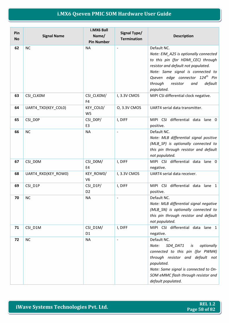
REL 1.2 Page 58 of 82
i.MX6 Qseven PMIC SOM Hardware User Guide
iWave Systems Technologies Pvt. Ltd.
Pin
No Signal Name
i.MX6 Ball
Name/
Pin Number
Signal Type/
Termination Description
62 NC NA - Default NC.
Note: EIM_A25 is optionally connected
to this pin (for HDMI_CEC) through
resistor and default not populated.
Note: Same signal is connected to
Qseven edge connector 124th Pin
through resistor and default
populated.
63 CSI_CLK0M CSI_CLK0M/
F4
I, 3.3V CMOS MIPI CSI differential clock negative.
64 UART4_TXD(KEY_COL0) KEY_COL0/
W5
O, 3.3V CMOS UART4 serial data transmitter.
65 CSI_D0P CSI_D0P/
E3
I, DIFF MIPI CSI differential data lane 0
positive.
66 NC NA - Default NC.
Note: MLB differential signal positive
(MLB_SP) is optionally connected to
this pin through resistor and default
not populated.
67 CSI_D0M CSI_D0M/
E4
I, DIFF MIPI CSI differential data lane 0
negative.
68 UART4_RXD(KEY_ROW0) KEY_ROW0/
V6
I, 3.3V CMOS UART4 serial data receiver.
69 CSI_D1P CSI_D1P/
D2
I, DIFF MIPI CSI differential data lane 1
positive.
70 NC NA - Default NC.
Note: MLB differential signal negative
(MLB_SN) is optionally connected to
this pin through resistor and default
not populated.
71 CSI_D1M CSI_D1M/
D1
I, DIFF MIPI CSI differential data lane 1
negative.
72 NC NA - Default NC.
Note: SD4_DAT1 is optionally
connected to this pin (for PWM4)
through resistor and default not
populated.
Note: Same signal is connected to On-
SOM eMMC flash through resistor and
default populated.

REL 1.2 Page 59 of 82
i.MX6 Qseven PMIC SOM Hardware User Guide
iWave Systems Technologies Pvt. Ltd.
Pin
No Signal Name
i.MX6 Ball
Name/
Pin Number
Signal Type/
Termination Description
73 CSI_D2P CSI_D2P/
E2
I, DIFF MIPI CSI differential data lane 2
positive.
74 CLK2_p CLK2_p/
D5
I, DIFF General purpose high speed
differential clock 2 positive.
75 CSI_D2M CSI_D2M/
E1
O, DIFF MIPI CSI differential data lane 2
negative.
76 CLK2_n CLK2_n/
C5
O, DIFF General purpose high speed
differential clock 2 negative
77 GND NA Power Ground.
78 GND NA Power Ground.
79 CSI_D3P CSI_D3P/
F1
I, DIFF MIPI CSI differential data lane 3
positive.
80 CSI_D3M CSI_D3M/
F2
I, DIFF MIPI CSI differential data lane 3
negative.
¹ Important Note: These signals are also used for i.MX6 CPU bootstrap setting on SOM and so no external loads or
pull-up/pull-down resistors to be connected to these pins which will change the boot configuration.
² Note: Termination value is mentioned based on SPI flash as boot media. If boot media is changed to other using
Boot media setting switch (SW1), termination value also may change.

REL 1.2 Page 60 of 82
i.MX6 Qseven PMIC SOM Hardware User Guide
iWave Systems Technologies Pvt. Ltd.
2.10 Optional Features
i.MX6 Qseven PMIC SOM has PCB footprint option for some features which are not supported by default. These
optional features are explained in the following sections.
To add any of these optional features in i.MX6 Qseven PMIC SOM, please contact iWave.
2.10.1 NAND Flash
i.MX6 Qseven PMIC SOM supports NAND flash memory as mass storage and also can be used as boot device. This is
connected to NAND flash controller of the i.MX6 CPU and operates at 3.3 voltage level. This is the optional feature
and will not be populated in default configuration.
Note: If NAND flash feature is required in the SOM, eMMC flash on SOM and signals to Qseven Pins 17, 19, 44, 46, 47,
53, 54, 55, 56, 70, 111, 112 & 156 cannot be used.
2.10.2 RTC Controller
i.MX6 Qseven PMIC SOM by default supports RTC from i.MX6 CPU. But i.MX6 RTC controller draws more power from
VCC_RTC coin cell power input (when VCC is off) and could drain the coin cell faster. So i.MX6 Qseven PMIC SOM
optionally supports external RTC Controller “BQ32000DR” On-SOM which will draw very less power compare to
i.MX6 RTC controller.
External RTC Controller is connected to the i.MX6 CPU through I2C2 Interface and operates at 3.3V voltage level. In
SOM power off condition, this device will take power from Qseven Edge (VCC_RTC) coin cell power input (Pin 193)
and continues to keep the current time. This is the optional feature and will not be populated in default
configuration.
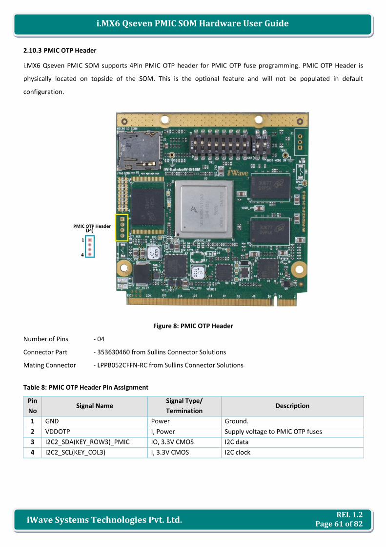
REL 1.2 Page 61 of 82
i.MX6 Qseven PMIC SOM Hardware User Guide
iWave Systems Technologies Pvt. Ltd.
2.10.3 PMIC OTP Header
i.MX6 Qseven PMIC SOM supports 4Pin PMIC OTP header for PMIC OTP fuse programming. PMIC OTP Header is
physically located on topside of the SOM. This is the optional feature and will not be populated in default
configuration.
Figure 8: PMIC OTP Header
Number of Pins - 04
Connector Part - 353630460 from Sullins Connector Solutions
Mating Connector - LPPB052CFFN-RC from Sullins Connector Solutions
Table 8: PMIC OTP Header Pin Assignment
Pin
No Signal Name
Signal Type/
Termination Description
1 GND Power Ground.
2 VDDOTP I, Power Supply voltage to PMIC OTP fuses
3 I2C2_SDA(KEY_ROW3)_PMIC IO, 3.3V CMOS I2C data
4 I2C2_SCL(KEY_COL3) I, 3.3V CMOS I2C clock

REL 1.2 Page 62 of 82
i.MX6 Qseven PMIC SOM Hardware User Guide
iWave Systems Technologies Pvt. Ltd.
2.10.4 JTAG Header
A customized 20-pin ARM JTAG connector is available in i.MX6 Qseven PMIC SOM for Debug purpose. 3.3V reference
power is provided to pin 1 of the connector to allow JTAG tool to automatically configure the logic signals for the
right voltage. JTAG connector is physically located on topside of the SOM. This is the optional feature and will not be
populated in default configuration.
Figure 9: JTAG Header
Number of Pins - 20
Connector Part - GRPB102MWCN-RC from Sullins Connector Solutions
Mating Connector - LPPB102CFFN-RC from Sullins Connector Solutions
Table 9: JTAG Header Pin Assignment
Pin
No Signal Name
Signal Type/
Termination Description
1 VCC_3V3 O, 3.3V Power VREF reference Voltage.
2 VCC_3V3 O, 3.3V Power Supply Voltage.
3 JTAG_TRSTB I, 3.3V CMOS JTAG test reset signal.
4 GND Power Ground.
5 JTAG_TDI I, 3.3V CMOS JTAG test data input.

REL 1.2 Page 63 of 82
i.MX6 Qseven PMIC SOM Hardware User Guide
iWave Systems Technologies Pvt. Ltd.
Pin
No Signal Name
Signal Type/
Termination Description
6 GND Power Ground.
7 JTAG_TMS I, 3.3V CMOS JTAG test mode select.
8 GND Power Ground.
9 JTAG_TCK I, 3.3V CMOS JTAG test Clock.
10 GND Power Ground.
11 - - NC.
12 GND Power Ground.
13 JTAG_TDO O, 3.3V CMOS JTAG test data output.
14 GND Power Ground.
15 JTAG_RESETB I, 3.3V CMOS Reset Signal.
16 GND Power Ground.
17 - - NC.
18 GND Power Ground.
19 - - NC.
20 GND Power Ground.
Table 10: JTAG Header - BOM
Sl.
No. Part Description Part Number Identifier Package Quantity
1 CONN HEADER .05" 20PS DL R/A GRPB102MWCN-RC J3 20Pin TH 1
2 IC BUFFER TRI-ST ULP N-INV NC7SP125P5X U13 SC-70-5 1
3 RES 0.0 OHM 1/16W JUMP RC0402JR-070RL R312,R309 0402 2
4 RES 10K OHM 1/16W 5% RC0402JR-0710KL R251 0402 1
5 CAP CER 0.1UF 10V 10% X5R CC0402KRX5R6BB104 C76 0402 1
6 CONN HEADER .050" 20PS DL PCB LPPB102CFFN-RC Mating for J3
connector
NA 1
Note: For i.MX6 Qseven PMIC SOM Silkscreen identifier details, refer APPENDIX I.

REL 1.2 Page 64 of 82
i.MX6 Qseven PMIC SOM Hardware User Guide
iWave Systems Technologies Pvt. Ltd.
2.10.5 Debug UART Header
i.MX6 Qseven PMIC SOM supports 3pin UART2 header (J1) for Debug purpose. This UART header supports only serial
data input and serial data output signals in RS232 level. This 3-Pin debug UART header is physically located on
topside of the SOM. This is the optional feature and will not be populated in default configuration.
Figure 10: Debug UART Header
Table 11: Debug UART Header Pin Assignment
Pin
No Signal Name
Signal Type/
Termination Description
1 GND Power Ground.
2 UART2_TXD O, RS232 UART2 serial data transmitter.
3 UART2_RXD I, RS232 UART2 serial data receiver.
Table 12: Debug UART Header - BOM
Sl.
No. Part Description Part Number Identifier Package Quantity
1 CONN HEADER 3POS 2MM R/A 35363-0360 J1 3Pin TH 1
2 IC DRVR/RCVR MLTCH RS232 MAX3232IPWR U11 16Pin TSSOP 1
3 CAP CER 0.1UF 10V 10% X5R CC0402KRX5R6BB104 C3,C84,C85,C86,
C87
0402 5
4 CAP CER 10UF 10V 20% X5R C1608X5R1A106M C4 0603 1
5 RES 0.0 OHM 1/16W JUMP RC0402JR-070RL R72,R74
Note: Remove
R71 & R73
0402 2
Note: For i.MX6 Qseven PMIC SOM Silkscreen identifier details, refer APPENDIX I.

REL 1.2 Page 65 of 82
i.MX6 Qseven PMIC SOM Hardware User Guide
iWave Systems Technologies Pvt. Ltd.
2.10.6 Power IN Connector
i.MX6 Qseven PMIC SOM works with +5V power input from Qseven Edge connector. Optionally SOM can be
powered up using Power IN Header (P1) for standalone purpose. This is the optional feature and will not be
populated in default configuration.
Figure 11: 2Pin Power Connector
Table 13: 2Pin Power Connector
Pin
No Signal Name
Signal Type/
Termination Description
1 VCC I, 5V Power Input Supply Voltage.
2 GND Power Ground.
Table 14: Power IN Connector - BOM
Sl.
No. Part Description Part Number Identifier Package Quantity
1 CONN HEADER VERT 2CKT 2.5MM 0099990986 P1 2Pin TH 1
2 FUSE FAST 24VDC 3A SF-0603F300-2 F1 0603 1
3 TVS ESD PROT ULT LOW CAP ESD9L5.0ST5G D8 SOD-923 1
4 CAP CER 0.1UF 10V 10% X5R CC0402KRX5R6BB104 C341 0402 1
5 CONN HOUSING 2POS 2.5MM
SHROUD
0050375023 Mating connector
for P1
NA 1
6 CONN FEMALE 22-28AWG
2.5MM TIN
0008701039 Mating connector
crimp pin
NA 2
Note: For i.MX6 Qseven PMIC SOM Silkscreen identifier details, refer APPENDIX I

REL 1.2 Page 66 of 82
i.MX6 Qseven PMIC SOM Hardware User Guide
iWave Systems Technologies Pvt. Ltd.
3. TECHNICAL SPECIFICATION
This section provides detailed information about the i.MX6 Qseven PMIC SOM technical specification with Electrical,
Environmental and Mechanical characteristics.
3.1 Electrical Characteristics
3.1.1 Power Input Requirement
The below table provides the Power Input Requirement of i.MX6 Qseven PMIC SOM.
Table 15: Power Input Requirement
Sl. No. Power Rail Min (V) Typical (V) Max(V) Max Input Ripple
1 VCC¹ 4.75V 5V 5.25V ±50mV
2 VCC_5V_SB² NC NC NC NC
3 VCC_RTC³ 2.8V 3V 3.3V ±20 mV
¹ i.MX6 Qseven PMIC SOM is designed to work with VCC input power rail from Qseven Edge connector. Optionally we
can use On-SOM Power In connector to feed VCC which can be used only for standalone power up.
² i.MX6 Qseven PMIC SOM doesn’t support VCC_5V_SB standby voltage input from Qseven Edge Connector.
³ i.MX6 Qseven PMIC SOM uses this voltage as backup power source to RTC when VCC is off.

REL 1.2 Page 67 of 82
i.MX6 Qseven PMIC SOM Hardware User Guide
iWave Systems Technologies Pvt. Ltd.
3.1.2 Power Input Sequencing
i.MX6 Qseven PMIC SOM’s Power Input sequence requirement is explained below.
Power up Sequence:
VCC_RTC must come up at the same time or before VCC comes up.
PWGIN signal from Qseven Edge must be active at the same time or after VCC comes up.
Power down Sequence:
PWGIN signal from Qseven Edge must be inactive at the same time or before VCC goes down.
VCC must go down at the same time or before VCC_RTC goes down.
Figure 12: Qseven SOM Power Sequence
Table 16: Power Sequence Timing
Item Description Value
T1 VCC_RTC rise time to VCC rise time ≥ 0 ms
T2 VCC rise time to PWGIN rise time ≥ 0 ms
T3 PWGIN fall time to VCC fall time ≥ 0 ms
T4 VCC fall time to VCC_RTC fall time ≥ 0 ms
Important Note: All carrier board power supplies should be powered ON only after the SOM is powered ON
completely. This is to ensure that there is no back voltage (leakage) from any supply on the board towards the CPU
GPIO pins which may affect the booting.

REL 1.2 Page 68 of 82
i.MX6 Qseven PMIC SOM Hardware User Guide
iWave Systems Technologies Pvt. Ltd.
3.1.3 Power Consumption
Table 17: Power Consumption¹
Task/Status Power Rail Current Drawn/Power Consumption
Run Mode Power Consumption
MP3 audio playback on AUDMUX4 VCC 0.35A/1.75W
1080p video playback on LVDS0 (WVGA LCD) VCC 0.48A/2.4W
1080p video playback on HDMI (1080p Monitor) VCC 0.57A/2.85W
OpenGL graphics application on LVDS0 VCC 0.66A/3.3W
Dhrystone benchmark application VCC 1.1A/5.5W
Typical Maximum Power:
MP3 audio playback.
1080p video playback on HDMI.
VGA video playback & OpenGL graphics
application on LVDS0
Gigabit Ethernet ping.
USB to Micro SD file transfer.
Dhrystone benchmark application
VCC 1.19A/5.95W
Low Power Mode Power Consumption
Deep Sleep Mode VCC 0.19A/950mW²
RTC power when no VCC supply is provided VCC_RTC 275uA³
¹ Power consumption measurements have been done in iWave’s i.MX6 Quad CPU based Qseven PMIC SOM (iW-
G15M-Q704-3D001G-E004G-LID) with iWave’s Generic Qseven Carrier board running iWave’s Linux3.10 BSP (iW-
PRDVZ-RN-01-R5.0-REL1.0-Linux3.10).
² Only i.MX6 CPU related power management is implemented in the BSP for low power mode.
³ i.MX6 RTC controller draws more power from VCC_RTC coin cell power input and so could drain the coin cell faster.

REL 1.2 Page 69 of 82
i.MX6 Qseven PMIC SOM Hardware User Guide
iWave Systems Technologies Pvt. Ltd.
3.2 Environmental Characteristics
3.2.1 Environmental Specification
The below table provides the Environment specification of i.MX6 Qseven PMIC SOM.
Table 18: Environmental Specification
Parameters Min Max
Operating temperature range¹ ² -40°C 85°C
Storage temperature range -40°C 85°C
Humidity - Operating 10%RH 90%RH
Humidity - Storage 5%RH 95%RH
¹ iWave guarantees the component selection for the given operating temperature. The operating temperature at the
system level will be affected by the various system components like carrier board and its components, system
enclosure, air circulation in the system, system power supply etc. Based on the system design, specific heat
dissipating approach might be required from system to system. It is recommended to do the necessary system level
thermal simulation and find necessary thermal solution in the system before using this board in the end application.
² For more information on Thermal solution & Heat spreader refer the following section.
3.2.2 Heat Spreader
For any highly integrated System On Modules, thermal design is very important factor. As IC’s size is decreasing and
performance of module is increasing by rising processor frequencies, it generates high amount of heat which should
be dissipated for the system to work as expected without fault.
To dissipate the heat, appropriate thermal management technique like Heat spreader, Heat sink must be used.
Always remember that, if you use more effective thermal solution, you will get more performance out of the CPU.
Heat spreader acts as thermal coupling device between Module and external thermal solution. Heat spreader also
provides thermal coupling to CPU via gap filler for better heat exchange. Heat spreader is not a complete thermal
solution by itself. Heat spreader has to be used with application specific thermal solutions like heat sinks, Chassis,
fans, Heat pipes etc.
iWave supports Heat Spreader Solution for i.MX6 Qseven PMIC SOM. Please refer the below figure for Heat spreader
dimension details. For Heat spreader ordering information, please refer section 4 ORDERING INFORMATION.
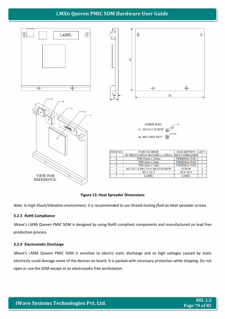
REL 1.2 Page 70 of 82
i.MX6 Qseven PMIC SOM Hardware User Guide
iWave Systems Technologies Pvt. Ltd.
Figure 13: Heat Spreader Dimensions
Note: In high Shock/Vibration environment, it is recommended to use thread-locking fluid on Heat spreader screws.
3.2.3 RoHS Compliance
iWave’s i.MX6 Qseven PMIC SOM is designed by using RoHS compliant components and manufactured on lead free
production process.
3.2.4 Electrostatic Discharge
iWave’s i.MX6 Qseven PMIC SOM is sensitive to electro static discharge and so high voltages caused by static
electricity could damage some of the devices on board. It is packed with necessary protection while shipping. Do not
open or use the SOM except at an electrostatic free workstation.
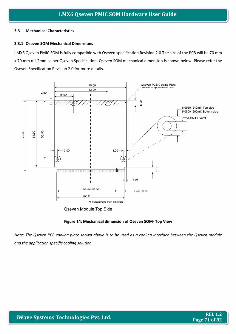
REL 1.2 Page 71 of 82
i.MX6 Qseven PMIC SOM Hardware User Guide
iWave Systems Technologies Pvt. Ltd.
3.3 Mechanical Characteristics
3.3.1 Qseven SOM Mechanical Dimensions
i.MX6 Qseven PMIC SOM is fully compatible with Qseven specification Revision 2.0.The size of the PCB will be 70 mm
x 70 mm x 1.2mm as per Qseven Specification. Qseven SOM mechanical dimension is shown below. Please refer the
Qseven Specification Revision 2.0 for more details.
Figure 14: Mechanical dimension of Qseven SOM- Top View
Note: The Qseven PCB cooling plate shown above is to be used as a cooling interface between the Qseven module
and the application specific cooling solution.

REL 1.2 Page 72 of 82
i.MX6 Qseven PMIC SOM Hardware User Guide
iWave Systems Technologies Pvt. Ltd.
Figure 15: Mechanical dimension of Qseven SOM- Bottom View
i.MX6 Qseven PMIC SOM PCB thickness is 1.2mm±0.15mm, top side maximum height component is boot switch
(4.34±0.29mm) followed by Power diode (2.43±0.45mm) and bottom side maximum height component is expansion
connector (4.30mm±0.15mm) followed by Crystal (1.9mm±0.15mm). Please refer the below figure which gives
height details of the i.MX6 Qseven PMIC SOM.
Figure 16: Mechanical dimension of Qseven SOM- Side View

REL 1.2 Page 73 of 82
i.MX6 Qseven PMIC SOM Hardware User Guide
iWave Systems Technologies Pvt. Ltd.
3.3.2 Guidelines to insert the Qseven SOM into Carrier board
Make sure that the carrier board is completely powered off.
Insert the Qseven module in to the MXM connector at an angle of 45° as shown below in the first photo.
Check the Notch position of Qseven module is proper while inserting.
Once the Qseven module is inserted to the MXM connector properly, press the board vertically down as
shown below (in the second photo), such that the board is fixed firmly into the expansion connectors.
Figure 17: Qseven Module Insertion procedure
Note: Photo shown above is for only reference and not exactly represents i.MX6 Qseven PMIC SOM.

REL 1.2 Page 74 of 82
i.MX6 Qseven PMIC SOM Hardware User Guide
iWave Systems Technologies Pvt. Ltd.
4. ORDERING INFORMATION
i.MX6 Qseven PMIC SOM is available in different variations. The below table provides the standard orderable part
numbers for different i.MX6 Qseven PMIC SOM variations. If the desired part number is not listed in below table, or
if any custom configuration part number is required, please contact iWave.
Table 19: Orderable Product Part Numbers
Product Part Number Description Temperature
i.MX6 QuadPlus CPU based Qseven PMIC SOMs
iW-G15M-Q74P-3D001G-E004G-LIC With i.MX6 Quad Plus Industrial grade CPU, 1GB RAM,
4GB eMMC with Linux - without expansion
Industrial
iW-G15M-Q74P-3D001G-E004G-AIC With i.MX6 Quad Plus Industrial grade CPU, 1GB RAM,
4GB eMMC with Android - without expansion
Industrial
iW-G15M-Q74P-3D001G-E004G-WIC With i.MX6 Quad Plus Industrial grade CPU, 1GB RAM,
4GB eMMC with WEC7 - without expansion
Industrial
iW-G15M-Q74P-3D001G-E004G-BIC With i.MX6 Quad Plus Industrial grade CPU, 1GB RAM,
4GB eMMC with boot code - without expansion
Industrial
iW-G15M-Q74P-3D002G-E004G-BIC With i.MX6 Quad Plus Industrial grade CPU, 2GB RAM,
4GB eMMC with boot code - without expansion
Industrial
iW-G15M-Q74P-3D001G-E004G-LID With i.MX6 Quad Plus Industrial grade CPU, 1GB RAM,
4GB eMMC with Linux - with expansion
Industrial
iW-G15M-Q74P-3D001G-E004G-AID With i.MX6 Quad Plus Industrial grade CPU, 1GB RAM,
4GB eMMC with Android - with expansion
Industrial
iW-G15M-Q74P-3D001G-E004G-WID With i.MX6 Quad Plus Industrial grade CPU, 1GB RAM,
4GB eMMC with WEC7 - with expansion
Industrial
iW-G15M-Q74P-3D001G-E004G-BID With i.MX6 Quad Plus Industrial grade CPU, 1GB RAM,
4GB eMMC with boot code - with expansion
Industrial
iW-G15M-Q74P-3D002G-E004G-BID With i.MX6 Quad Plus Industrial grade CPU, 2GB RAM,
4GB eMMC with boot code - with expansion
Industrial
i.MX6 Quad CPU based Qseven PMIC SOMs
iW-G15M-Q704-3D001G-E004G-LIC With i.MX6 Quad Core Automotive grade CPU, 1GB RAM,
4GB eMMC with Linux - without expansion
Industrial
iW-G15M-Q704-3D001G-E004G-AIC With i.MX6 Quad Core Automotive grade CPU, 1GB RAM,
4GB eMMC with Android - without expansion
Industrial
iW-G15M-Q704-3D001G-E004G-WIC With i.MX6 Quad Core Automotive grade CPU, 1GB RAM,
4GB eMMC with WEC7 - without expansion
Industrial
iW-G15M-Q704-3D001G-E004G-BIC With i.MX6 Quad Core Automotive grade CPU, 1GB RAM,
4GB eMMC with boot code - without expansion
Industrial
iW-G15M-Q704-3D002G-E004G-BIC With i.MX6 Quad Core Automotive grade CPU, 2GB RAM,
4GB eMMC with boot code - without expansion
Industrial
iW-G15M-Q704-3D001G-E004G-LID With i.MX6 Quad Core Automotive grade CPU, 1GB RAM,
4GB eMMC with Linux - with expansion
Industrial

REL 1.2 Page 75 of 82
i.MX6 Qseven PMIC SOM Hardware User Guide
iWave Systems Technologies Pvt. Ltd.
Product Part Number Description Temperature
iW-G15M-Q704-3D001G-E004G-AID With i.MX6 Quad Core Automotive grade CPU, 1GB RAM,
4GB eMMC with Android - with expansion
Industrial
iW-G15M-Q704-3D001G-E004G-WID With i.MX6 Quad Core Automotive grade CPU, 1GB RAM,
4GB eMMC with WEC7 - with expansion
Industrial
iW-G15M-Q704-3D001G-E004G-BID With i.MX6 Quad Core Automotive grade CPU, 1GB RAM,
4GB eMMC with boot code - with expansion
Industrial
iW-G15M-Q704-3D002G-E004G-BID With i.MX6 Quad Core Automotive grade CPU, 2GB RAM,
4GB eMMC with boot code - with expansion
Industrial
i.MX6 DualPlus CPU based Qseven PMIC SOMs
iW-G15M-Q72P-3D001G-E004G-LIC i.MX6 Dual Plus Industrial grade CPU, 1GB RAM, 4GB
eMMC with Linux - without expansion
Industrial
iW-G15M-Q72P-3D001G-E004G-AIC i.MX6 Dual Plus Industrial grade CPU, 1GB RAM, 4GB
eMMC with Android - without expansion
Industrial
iW-G15M-Q72P-3D001G-E004G-WIC i.MX6 Dual Plus Industrial grade CPU, 1GB RAM, 4GB
eMMC with WEC7 - without expansion
Industrial
iW-G15M-Q72P-3D001G-E004G-BIC i.MX6 Dual Plus Industrial grade CPU, 1GB RAM, 4GB
eMMC with boot code - without expansion
Industrial
iW-G15M-Q72P-3D002G-E004G-BIC i.MX6 Dual Plus Industrial grade CPU, 2GB RAM, 4GB
eMMC with boot code - without expansion
Industrial
iW-G15M-Q72P-3D001G-E004G-LID i.MX6 Dual Plus Industrial grade CPU, 1GB RAM, 4GB
eMMC with Linux - with expansion
Industrial
iW-G15M-Q72P-3D001G-E004G-AID i.MX6 Dual Plus Industrial grade CPU, 1GB RAM, 4GB
eMMC with Android - with expansion
Industrial
iW-G15M-Q72P-3D001G-E004G-WID i.MX6 Dual Plus Industrial grade CPU, 1GB RAM, 4GB
eMMC with WEC7 - with expansion
Industrial
iW-G15M-Q72P-3D001G-E004G-BID i.MX6 Dual Plus Industrial grade CPU, 1GB RAM, 4GB
eMMC with boot code - with expansion
Industrial
iW-G15M-Q72P-3D002G-E004G-BID i.MX6 Dual Plus Industrial grade CPU, 2GB RAM, 4GB
eMMC with boot code - with expansion
Industrial
i.MX6 Dual CPU based Qseven PMIC SOMs
iW-G15M-Q702-3D001G-E004G-LIC With i.MX6 Dual Core Automotive grade CPU, 1GB RAM,
4GB eMMC with Linux - without expansion
Industrial
iW-G15M-Q702-3D001G-E004G-AIC With i.MX6 Dual Core Automotive grade CPU, 1GB RAM,
4GB eMMC with Android - without expansion
Industrial
iW-G15M-Q702-3D001G-E004G-WIC With i.MX6 Dual Core Automotive grade CPU, 1GB RAM,
4GB eMMC with WEC7 - without expansion
Industrial
iW-G15M-Q702-3D001G-E004G-BIC With i.MX6 Dual Core Automotive grade CPU, 1GB RAM,
4GB eMMC with boot code - without expansion
Industrial
iW-G15M-Q702-3D002G-E004G-BIC With i.MX6 Dual Core Automotive grade CPU, 2GB RAM,
4GB eMMC with boot code - without expansion
Industrial
iW-G15M-Q702-3D001G-E004G-LID With i.MX6 Dual Core Automotive grade CPU, 1GB RAM,
4GB eMMC with Linux - with expansion
Industrial
REL 1.2 Page 76 of 82
i.MX6 Qseven PMIC SOM Hardware User Guide
iWave Systems Technologies Pvt. Ltd.
Product Part Number Description Temperature
iW-G15M-Q702-3D001G-E004G-AID With i.MX6 Dual Core Automotive grade CPU, 1GB RAM,
4GB eMMC with Android - with expansion
Industrial
iW-G15M-Q702-3D001G-E004G-WID With i.MX6 Dual Core Automotive grade CPU, 1GB RAM,
4GB eMMC with WEC7 - with expansion
Industrial
iW-G15M-Q702-3D001G-E004G-BID With i.MX6 Dual Core Automotive grade CPU, 1GB RAM,
4GB eMMC with boot code - with expansion
Industrial
iW-G15M-Q702-3D002G-E004G-BID With i.MX6 Dual Core Automotive grade CPU, 2GB RAM,
4GB eMMC with boot code - with expansion
Industrial
i.MX6 Duallite CPU based Qseven PMIC SOMs
iW-G15M-Q72L-3D001G-E004G-LIC With i.MX6 Dual Lite Industrial grade CPU, 1GB RAM, 4GB
eMMC with Linux - without expansion
Industrial
iW-G15M-Q72L-3D001G-E004G-AIC With i.MX6 Dual Lite Industrial grade CPU, 1GB RAM, 4GB
eMMC with Android - without expansion
Industrial
iW-G15M-Q72L-3D001G-E004G-WIC With i.MX6 Dual Lite Industrial grade CPU, 1GB RAM, 4GB
eMMC with WEC7 - without expansion
Industrial
iW-G15M-Q72L-3D001G-E004G-BIC With i.MX6 Dual Lite Industrial grade CPU, 1GB RAM, 4GB
eMMC with boot code - without expansion
Industrial
iW-G15M-Q72L-3D001G-E004G-LID With i.MX6 Dual Lite Industrial grade CPU, 1GB RAM, 4GB
eMMC with Linux - with expansion
Industrial
iW-G15M-Q72L-3D001G-E004G-AID With i.MX6 Dual Lite Industrial grade CPU, 1GB RAM, 4GB
eMMC with Android - with expansion
Industrial
iW-G15M-Q72L-3D001G-E004G-WID With i.MX6 Dual Lite Industrial grade CPU, 1GB RAM, 4GB
eMMC with WEC7 - with expansion
Industrial
iW-G15M-Q72L-3D001G-E004G-BID With i.MX6 Dual Lite Industrial grade CPU, 1GB RAM, 4GB
eMMC with boot code - with expansion
Industrial
i.MX6 Solo CPU based Qseven PMIC SOMs
iW-G15M-Q701-3D512M-E004G-LIC With i.MX6 Solo Core Industrial grade CPU, 512MB RAM,
4GB eMMC with Linux - without expansion
Industrial
iW-G15M-Q701-3D512M-E004G-AIC With i.MX6 Solo Core Industrial grade CPU, 512MB RAM,
4GB eMMC with Android - without expansion
Industrial
iW-G15M-Q701-3D512M-E004G-WIC With i.MX6 Solo Core Industrial grade CPU, 512MB RAM,
4GB eMMC with WEC7 - without expansion
Industrial
iW-G15M-Q701-3D512M-E004G-BIC With i.MX6 Solo Core Industrial grade CPU, 512MB RAM,
4GB eMMC with boot code - without expansion
Industrial
iW-G15M-Q701-3D512M-E004G-LID With i.MX6 Solo Core Industrial grade CPU, 512MB RAM,
4GB eMMC with Linux - with expansion
Industrial
iW-G15M-Q701-3D512M-E004G-AID With i.MX6 Solo Core Industrial grade CPU, 512MB RAM,
4GB eMMC with Android - with expansion
Industrial
iW-G15M-Q701-3D512M-E004G-WID With i.MX6 Solo Core Industrial grade CPU, 512MB RAM,
4GB eMMC with WEC7 - with expansion
Industrial
iW-G15M-Q701-3D512M-E004G-BID With i.MX6 Solo Core Industrial grade CPU, 512MB RAM,
4GB eMMC with boot code - with expansion
Industrial

REL 1.2 Page 77 of 82
i.MX6 Qseven PMIC SOM Hardware User Guide
iWave Systems Technologies Pvt. Ltd.
Product Part Number Description Temperature
Heat Spreader
iW-HSPALU-CLASLR-Q706 Heat Spreader for i.MX6DL/S Qseven PMIC SOM -
iW-HSPALU-CLASLR-Q707 Heat Spreader for i.MX6Q/D Qseven PMIC SOM -
Important Note: Some of the above mentioned Part Numbers are subject to MOQ purchase. Please contact iWave for
further details.
Note: For SOM identification purpose, Product Part Number and SOM Unique Serial Number are pasted as Label with
Barcode readable format on SOM.

REL 1.2 Page 78 of 82
i.MX6 Qseven PMIC SOM Hardware User Guide
iWave Systems Technologies Pvt. Ltd.
5. MIGRATION INFORMATION
This section provides the information needed for migrating i.MX6 Qseven Non PMIC SOM based design to newer
feature upgraded i.MX6 Qseven PMIC SOM. The below table provides the complete feature differences between
these SOMs.
Table 20: Differences between i.MX6 Qseven Non PMIC SOM and i.MX6 Qseven PMIC SOM
Sl. No Features i.MX6 Qseven Non PMIC SOM i.MX6 Qseven PMIC SOM
On – SOM Features
1 On-SOM power circuit Discrete power regulators are used
for powering i.MX6 CPU and On-
SOM peripherals.
Freescale’s PMIC
(MMPF0100F0ANES) is used for
powering i.MX6 CPU and On-SOM
peripherals for better power
Management.
2 Gigabit Ethernet PHY
Transceiver
KSZ9021 part from Micrel is used
for Gigabit Ethernet PHY
transceiver.
KSZ9031 part from Micrel is used
for Gigabit Ethernet PHY
transceiver.
3 PCB footprint option in SOM
for optional features
Footprint options are provided for,
JTAG Header
Debug UART Header
Power IN Connector
Footprint options are provided for,
NAND Flash
External RTC Controller
PMIC OTP Header
JTAG Header
Debug UART Header
Power IN Connector
Qseven Edge connector Pin out
4 Qseven Specification version
compatibility
Qseven Specification version R1.2
compatible.
Qseven Specification version R2.0
compatible by adding Data UART &
8 GPIOs.
5 Data UART (with CTS & RTS)
support on Qseven Edge
connector pins 171, 172, 177
& 178.
Data UART (with CTS & RTS)
support on Qseven Edge connector
pins 171, 172, 177 & 178 are
depopulated by default.
Data UART (with CTS & RTS)
support on Qseven Edge connector
pins 171, 172, 177 & 178 are
populated by default.
6 8 GPIOs support on Qseven
Edge connector pins 185 to
192.
Qseven Edge connector pins 185 to
192 are NC.
Qseven Edge connector pins 185 to
192 are supported with 8 i.MX6
CPU GPIOs by default.
7 Ethernet GBE_CTREF
reference voltage on Qseven
Edge connector pin 15
GBE_CTREF reference voltage on
Qseven Edge connector pin 15 is
populated by default.
GBE_CTREF reference voltage on
Qseven Edge connector pin 15 is
depopulated by default.
8 Tamper Detection Input
support to i.MX6 CPU from
Qseven Edge connector pin
154.
Qseven Edge connector pin 154 is
NC.
Tamper Detection Input to i.MX6
CPU from Qseven Edge connector
pin 154 is populated by default.

REL 1.2 Page 79 of 82
i.MX6 Qseven PMIC SOM Hardware User Guide
iWave Systems Technologies Pvt. Ltd.
Sl. No Features i.MX6 Qseven Non PMIC SOM i.MX6 Qseven PMIC SOM
Expansion connector1 Pin out
9 CAN2 support on Expansion
connector1
CAN2 support on Expansion
connector1 pins 78 & 79 is
populated by default.
CAN2 support on Expansion
connector1 pins 78 & 79 is
depopulated by default.
10 Signals on Expansion
connector1 pins 3, 11, 13, 15
& 19
Signals on Expansion connector1
pins 3, 11, 13, 15 & 19 are
populated by default.
Signals on Expansion connector1
pins 3, 11, 13, 15 & 19 are
depopulated by default.
11 Signals of Expansion
connector1 pins 5, 7, 9 & 14
Signals of Expansion connector1
pins 5, 7, 9 & 14 are not shared
with Qseven pins.
Signals of Expansion connector1
pins 5, 7, 9 & 14 are also shared
with Qseven pins 192, 191, 190 &
189 respectively.
Expansion connector2 Pin out
12 Signals on Expansion
connector2 pins 3, 7, 11, 40,
62 & 72
Signals on Expansion connector2
pins 3, 7, 11, 40, 62 & 72 are
populated by default.
Signals on Expansion connector2
pins 3, 7, 11, 40, 62 & 72 are
depopulated by default.
Mechanical
13 Mechanical dimension Mechanical dimension is 70mm x
70mm.
Mechanical dimension is 70mm x
70mm same as i.MX6 Qseven Non
PMIC SOM with only change in
component’s placement and height
profile.
Important Note: iWave’s existing BSP releases for i.MX6 Qseven Non PIMC SOM is compatible with additional
software patches for i.MX6 Qseven PIMC SOM to support above mentioned differences. Also all future BSP release by
iWave will be compatible for both the SOMs until further notice.

REL 1.2 Page 80 of 82
i.MX6 Qseven PMIC SOM Hardware User Guide
iWave Systems Technologies Pvt. Ltd.
6. APPENDIX I
6.1 i.MX6 Qseven PMIC SOM Silk Screen
i.MX6 Qseven PMIC SOM’s PCB silkscreen top view and bottom view are shown in the below figures to identify the
optional feature’s location on SOM. This will be helpful for mounting the optional features in i.MX6 Qseven PMIC
SOM.
Figure 18: Silk Screen Top View

REL 1.2 Page 81 of 82
i.MX6 Qseven PMIC SOM Hardware User Guide
iWave Systems Technologies Pvt. Ltd.
Figure 19: Silk Screen Bottom View

REL 1.2 Page 82 of 82
i.MX6 Qseven PMIC SOM Hardware User Guide
iWave Systems Technologies Pvt. Ltd.
7. APPENDIX II
7.1 i.MX6 Qseven PMIC SOM Development Platform
iWave Systems supports Generic Qseven Carrier Board which is targeted for quick validation of high performance
Qseven compatible CPU modules. Being a Nano-ITX form factor with 120mmx120mm size, the carrier board is highly
packed with all necessary interfaces & on-board connectors to validate complete Qseven supported features.
iWave Systems supports iW-RainboW-G15D – i.MX6 Qseven Development Platform with i.MX6 Qseven PMIC SOM
and Generic Qseven Carrier board for complete validation of i.MX6 Qseven PMIC SOM functionality with complete
BSP support. For more details on i.MX6 Qseven PMIC SOM Development platform, visit the below web link.
http://www.iwavesystems.com/product/development-platform/i-mx6-q7-development-kit-18/i-mx6-q7-
development-kit.html
Figure 20: i.MX6 Qseven PMIC SOM Development Platform