pmic with integrated chargers and smart power selector in
TRANSCRIPT
General DescriptionThe MAX8819_ is a complete power solution for MP3players and other handheld applications. The ICincludes a battery charger, step-down converters, andWLED power. It features an input current-limit switch topower the IC from an AC-to-DC adapter or USB port, a1-cell lithium ion (Li+) or lithium polymer (Li-Poly) charg-er, three step-down converters, and a step-up converterwith serial step dimming for powering two to six whiteLEDs. All power switches for charging and switching thesystem load between battery and external power areincluded on-chip. No external MOSFETs are required.The MAX8819C/MAX8819D offer a sequenced power-up/power-down of OUT1, OUT2, and then OUT3.
Maxim’s Smart Power Selector™ makes the best use ofAC-to-DC adapter power or limited USB power. Batterycharge current and input current limit are independent-ly set. Input power not used by the system charges thebattery. Charge current is resistor programmable andthe input current limit can be selected as 100mA,500mA, or 1A. Automatic input selection switches thesystem load from battery to external power. In addition,on-chip thermal limiting reduces the battery charge rateto prevent charger overheating.
ApplicationsMP3 Players
Portable GPS Devices
Low-Power Handheld Products
Cellular Telephones
Digital Cameras
Handheld Instrumentation
PDAs
Features♦ Smart Power Selector♦ Operates with No Battery Present♦ USB/AC Adapter One-Cell Li+ Charger♦ Three 2MHz Step-Down Converters
95% Peak Efficiency100% Duty Cycle±3% Output Accuracy over Load/Line/
Temperature♦ 2 to 6 Series WLED Driver with Dimming Control♦ RST1 Output♦ Short-Circuit/Thermal-Overload/Input
Undervoltage/Overvoltage Protection♦ Power-Up Sequencing (MAX8819C/MAX8819D)♦ Total Solution Size: Less Than 90mm2
MA
X8
81
9A
–MA
X8
81
9D
PMIC with Integrated Chargers and SmartPower Selector in a 4mm x 4mm TQFN
________________________________________________________________ Maxim Integrated Products 1
19-4166; Rev 0; 6/08
For pricing, delivery, and ordering information, please contact Maxim Direct at 1-888-629-4642,or visit Maxim’s website at www.maxim-ic.com.
Pin Configuration appears at end of data sheet.
Smart Power Selector is a trademark of Maxim IntegratedProducts, Inc.
USB/AC-TO-DCADAPTER
ENABLE SYSTEM
ENABLE CHARGER
ENABLE BACKLIGHT
SYS
DC
DLIM1
DLIM2
EN123
CEN
EN4
LX4
OVP4
FB4
LX3
LX2
CISET
BAT
SYS
Li+/Li-PolyBATTERY
OUT1I/O
OUT2MEMORY
OUT3CORE
CHG CHG
LX1
RST1 RST1
MAX8819_
+
Typical Operating Circuit
Ordering Information
+Denotes a lead-free/RoHS-compliant package.*Future product—contact factory for availability.**EP = Exposed pad.
PART TEMP RANGE PIN-PACKAGE
SYSVOLTAGE
(V)
MAX8819AETI+ -40°C to +85°C 28 TQFN-EP** 4.35MAX8819BETI+ -40°C to +85°C 28 TQFN-EP** 5.3
MAX8819CETI+ -40°C to +85°C 28 TQFN-EP** 4.35MAX8819DETI+ -40°C to +85°C 28 TQFN-EP** 5.3
EVALUATION KITAVAILABLE

MA
X8
81
9A
–MA
X8
81
9D
PMIC with Integrated Chargers and SmartPower Selector in a 4mm x 4mm TQFN
2 _______________________________________________________________________________________
ELECTRICAL CHARACTERISTICS(DC, LX_ unconnected; VEP = VGND = 0V, VBAT = 4V, DLIM[1:2] = 00, EN123 = EN4 = low, VFB1 = VFB2 = VFB3 = 1.1V, VFB4 = 0.6V,PV13 = PV2 = SYS, TA = -40°C to +85°C, capacitors as shown in Figure 1, RCISET = 3kΩ, unless otherwise noted.) (Note 3)
Stresses beyond those listed under “Absolute Maximum Ratings” may cause permanent damage to the device. These are stress ratings only, and functionaloperation of the device at these or any other conditions beyond those indicated in the operational sections of the specifications is not implied. Exposure toabsolute maximum rating conditions for extended periods may affect device reliability.
PARAMETER SYMBOL CONDITIONS MIN TYP MAX UNITS
DC POWER INPUT
DC Voltage Range VDC 4.1 5.5 V
MAX8819A/MAX8819C 4.3 4.35 4.4SYS Regulation Voltage VSYS_REG VDC = 5.75V
MAX8819B/MAX8819D 5.1 5.3 5.5V
DC Undervoltage Threshold VUVLO_DC VDC rising, 500mV typical hysteresis 3.95 4.00 4.05 V
DC Overvoltage Threshold VOVLO_DC VDC rising, 300mV typical hysteresis 5.811 5.9 6.000 V
DLIM[1:2] = 10 90 95 100
DLIM[1:2] = 01 450 475 500DC Current Limit(Note 4)
IDCLIM
VDC = 5.75V, VSYS = 5Vfor MAX8819B/MAX8819Dor VSYS = 4V forMAX8819A/MAX8819C DLIM[1:2] = 00 900 1000 1100
mA
DLIM[1:2] = 11 (suspend) 0.02 0.035
DLIM[1:2] ≠ 11, ISYS = 0mA, IBAT = 0mA,EN123 = low, EN4 = low, CEN = high,VDC = 5.5V
1.33DC Quiescent Current IDCIQ
DLIM[1:2] ≠ 11, ISYS = 0mA, EN123 = low,EN4 = low, CEN = low, VDC = 5.5V
0.95
mA
DC-to-SYS Dropout Resistance RDS VDC = 4V, ISYS = 400mA, DLIM[1:2] = 01 0.330 0.700 Ω
DC-to-SYS Soft-Start Time tSS-D-S 1.5 ms
DC Thermal-Limit TemperatureDie temperature where current limit isreduced
100 °C
DC Thermal-Limit GainAmount of input current reduction abovethermal-limit temperature
5 %/°C
SYSTEM
System Operating Voltage Range VSYS 2.6 5.5 V
ABSOLUTE MAXIMUM RATINGSDC, SYS, BAT, CISET, DLIM1, DLIM2, EN123
CEN, EN4, CHG, RST1, FB1, FB2, FB3 to GND....-0.3V to +6VPV2 to GND...............................................-0.3V to (VSYS + 0.3V)PV13 to SYS...........................................................-0.3V to +0.3VPG1, PG2, PG3, PG4 to GND................................-0.3V to +0.3VCOMP4, FB4 to GND ................................-0.3V to (VSYS + 0.3V)LX4 to PG4 .............................................................-0.3V to +33V OVP4 to GND .........................................................-0.3V to +33VLX1, LX2, LX3 Continuous Current (Note 1) .........................1.5ALX4 Current ................................................................750mARMSOutput Short-Circuit Duration.....................................Continuous
Continuous Power Dissipation (TA = +70°C)28-Pin Thin QFN Single-Layer Board (derate 20.8mW/°C above +70°C)...........................................................1666.7mW28-Pin Thin QFN Multilayer Board (derate 28.6mW/°C above +70°C)...........................................................2285.7mW
Junction-to-Case Thermal Resistance (θJC) (Note 2)28-Lead Thin QFN...........................................................3°C/W
Operating Temperature Range ...........................-40°C to +85°CJunction Temperature........................................-40°C to +125°CStorage Temperature.........................................-65°C to +150°CLead Temperature (soldering, 10s) .................................+300°C
Note 1: LX1, LX2, LX3 have clamp diodes to their respective PG_ and PV_. Applications that forward bias these diodes must takecare not to exceed the package power dissipation limits.
Note 2: Package thermal resistances were obtained using the method described in JEDEC specification JESD51-7, using a four-layerboard. For detailed information on package thermal considerations, refer to http://www.maxim-ic.com/thermal-tutorial.

MA
X8
81
9A
–MA
X8
81
9D
PMIC with Integrated Chargers and SmartPower Selector in a 4mm x 4mm TQFN
_______________________________________________________________________________________ 3
PARAMETER SYMBOL CONDITIONS MIN TYP MAX UNITS
System Undervoltage LockoutThreshold
VUVLO_SYS VSYS falling, 100mV hysteresis 2.45 2.5 2.55 V
BAT-to-SYS Reverse RegulationVoltage
VBSRED
DC and BAT are delivering current to SYS;IBAT = 95mA; VDC = 4.3V,MAX8819A/MAX8819C (only)
50 66 90 mV
VDC = 0V, EN123 = low, EN4 = low,VBAT = 4V
10 20
VDC = 5V, DLIM[1:2] = 11, EN123 = low,EN4 = low, VBAT = 4V
0 10
VDC = 0V, EN123 = high, EN4 = low,VBAT = 4V (step-down converters are not indropout)
128 290Quiescent Current IPV+ISYS
VDC = 0V, EN123 = high, EN4 = high,VBAT = 4V (step-down converters are not indropout)
362 730
μA
BATTERY CHARGER (VDC = 5.0V)
BAT-to-SYS On-Resistance RBS VDC = 0V, VBAT = 4.2V, ISYS = 0.9A 0.073 0.165 ΩTA = +25°C 4.174 4.200 4.221BAT Regulation Voltage
(Figure 2)VBATREG
TA = -40°C to +85°C 4.158 4.200 4.242V
BAT Recharge Threshold (Note 4) -135 -100 -65 mV
BAT Prequalification Threshold VBATPRQ VBAT rising, 180mV hysteresis, Figure 2 2.9 3.0 3.1 V
RCISET Resistance RangeGuaranteed by BAT fast-charge currentlimit
3 15 kΩ
CISET Voltage VCISET RCISET = 7.5kΩ, IBAT = 267mA 0.9 1.0 1.1 V
DLIM[1:2] = 10, RCISET = 3kΩ 87 92 100
DLIM[1:2] = 01, RCISET = 3kΩ 450 472 500
DLIM[1:2] = 00, RCISET = 15kΩ 170 200 230
DLIM[1:2] = 00, RCISET = 7.5kΩ 375 400 425
BAT Fast-Charge Current Limit
DLIM[1:2] = 00, RCISET = 3.74kΩ 740 802 860
mA
BAT Prequalification Current VBAT = 2.5V, RCISET = 3.74kΩ 60 82 105 mA
Top-Off Threshold (Note 5) TA = +25°C, RCISET = 3.74kΩ 60 82 105 mA
VDC = 0V, EN123 = low, EN4 = low,CEN = low, VBAT = 4V
10 20
BAT Leakage CurrentVDC = 5V, DLIM[1:2] = 11, EN123 = low,EN4 = low, VBAT = 4V
0
μA
ELECTRICAL CHARACTERISTICS (continued)(DC, LX_ unconnected; VEP = VGND = 0V, VBAT = 4V, DLIM[1:2] = 00, EN123 = EN4 = low, VFB1 = VFB2 = VFB3 = 1.1V, VFB4 = 0.6V,PV13 = PV2 = SYS, TA = -40°C to +85°C, capacitors as shown in Figure 1, RCISET = 3kΩ, unless otherwise noted.) (Note 3)
MA
X8
81
9A
–MA
X8
81
9D
PMIC with Integrated Chargers and SmartPower Selector in a 4mm x 4mm TQFN
4 _______________________________________________________________________________________
ELECTRICAL CHARACTERISTICS (continued)(DC, LX_ unconnected; VEP = VGND = 0V, VBAT = 4V, DLIM[1:2] = 00, EN123 = EN4 = low, VFB1 = VFB2 = VFB3 = 1.1V, VFB4 = 0.6V,PV13 = PV2 = SYS, TA = -40°C to +85°C, capacitors as shown in Figure 1, RCISET = 3kΩ, unless otherwise noted.) (Note 3)
PARAMETER SYMBOL CONDITIONS MIN TYP MAX UNITS
Slew rate 333 mA/ms
Time from 0 to 500mA 1.5
Time from 0 to 100mA 0.3Charger Soft-Start Time tSS_CHG
Time from 100mA to 500mA 1.2
ms
Timer Accuracy +15 %
Timer Suspend ThresholdCISET voltage when the fast-charge timersuspends; 300mV translates to 20% of themaximum fast-charge current limit
250 300 350 mV
Timer Extend ThresholdCISET voltage when the fast-charge timerextends; 750mV translates to 50% of themaximum fast-charge current limit
700 750 800 mV
Prequalification Time tPQ 33 min
Fast-Charge Time tFC 660 min
Top-Off Time tTO 33 min
POWER SEQUENCING (Figures 6 and 7)
REG1, REG2, REG3 Soft-StartTime
tSS1, tSS2,tSS3
2.6 ms
REG4 Soft-Start Time tSS4 CCOMP4 = 0.022μF to GND 5 ms
REGULATOR THERMAL SHUTDOWN
Thermal Shutdown Temperature TJ rising +165 °C
Thermal Shutdown Hysteresis 15 °C
REG1–SYNCHRONOUS STEP-DOWN CONVERTER
Input Voltage PV13 supplied from SYS VSYS V
MAX8819A/MAX8819B 400Maximum Output Current
L = 4.7μH,RLSR = 0.13Ω(Note 6) MAX8819C/MAX8819D 550
mA
Short-Circuit Current L = 4.7μH, RLSR = 0.13Ω 600 mA
Short-Circuit Detection Threshold 230 mV
Short-Circuit Foldback Frequency fOSC/3 Hz
FB1 Voltage (Note 7) 0.997 1.01 1.028 V
Output Voltage Range 1 VSYS V
TA = +25°C -50 -5 +50FB1 Leakage Current VFB1 = 1.01V
TA = +85°C -10nA
Load Regulation IOUT1 = 100mA to 300mA 1 %
Line Regulation (Note 9) 1 %/D
p-Channel On-Resistance VPV13 = 4.0V, ILX1 = 180mA 190 mΩn-Channel On-Resistance VPV13 = 4.0V, ILX1 = 180mA 250 mΩ
MAX8819A/MAX8819B 0.565 0.600 0.640p-Channel Current-LimitThreshold MAX8819C/MAX8819D 0.615 0.650 0.750
A

MA
X8
81
9A
–MA
X8
81
9D
ELECTRICAL CHARACTERISTICS (continued)(DC, LX_ unconnected; VEP = VGND = 0V, VBAT = 4V, DLIM[1:2] = 00, EN123 = EN4 = low, VFB1 = VFB2 = VFB3 = 1.1V, VFB4 = 0.6V,PV13 = PV2 = SYS, TA = -40°C to +85°C, capacitors as shown in Figure 1, RCISET = 3kΩ, unless otherwise noted.) (Note 3)
PARAMETER SYMBOL CONDITIONS MIN TYP MAX UNITS
Skip-Mode Transition Current (Note 8) 80 mA
n-Channel Zero-CrossingThreshold
10 mA
Maximum Duty Cycle 100 %
Minimum Duty Cycle 12.5 %
PWM Frequency fOSC 1.8 2.0 2.2 MHz
Internal Discharge Resistance inShutdown
EN123 = low, resistance from LX1 to PG1 1.0 kΩ
REG2–SYNCHRONOUS STEP-DOWN CONVERTER
Input Voltage PV2 supplied from SYS VSYS V
MAX8819A/MAX8819B 300Maximum Output Current
L = 4.7μH,RLSR = 0.13Ω(Note 6) MAX8819C/MAX8819D 500
mA
Short-Circuit Current L = 4.7μH, RLSR = 0.13Ω 600 mA
Short-Circuit Detection Threshold 230 mV
Short-Circuit Foldback Frequency fOSC/3 Hz
FB2 Voltage (Note 7) 0.997 1.012 1.028 V
Output Voltage Range 1 VSYS V
TA = +25°C -50 -5 +50FB2 Leakage Current VFB2 = 1.01V
TA = +85°C -50nA
Load Regulation IOUT2 = 100mA to 300mA 1 %
Line Regulation (Note 9) 1 %/D
p-Channel On-Resistance VPV2 = 4.0V, ILX2 = 180mA 290 mΩn-Channel On-Resistance VPV2 = 4.0V, ILX2 = 180mA 200 mΩ
MAX8819A/MAX8819B 0.512 0.550 0.595p-Channel Current-LimitThreshold MAX8819C/MAX8819D 0.565 0.600 0.700
A
Skip-Mode Transition Current (Note 8) 80 mA
n-Channel Zero-CrossingThreshold
10 mA
Maximum Duty Cycle 100 %
Minimum Duty Cycle 12.5 %
PWM Frequency fOSC 1.8 2.0 2.2 MHz
Internal Discharge Resistance inShutdown
EN123 = low, resistance from LX2 to PG2 1.0 kΩ
REG2 Disable ΔISYS VPV2 = 0V, REG2 disabled (Note 10) -25 μA
REG3–SYNCHRONOUS STEP-DOWN CONVERTER
Input Voltage PV13 supplied from SYS VSYS V
PMIC with Integrated Chargers and SmartPower Selector in a 4mm x 4mm TQFN
_______________________________________________________________________________________ 5

MA
X8
81
9A
–MA
X8
81
9D
PMIC with Integrated Chargers and SmartPower Selector in a 4mm x 4mm TQFN
6 _______________________________________________________________________________________
ELECTRICAL CHARACTERISTICS (continued)(DC, LX_ unconnected; VEP = VGND = 0V, VBAT = 4V, DLIM[1:2] = 00, EN123 = EN4 = low, VFB1 = VFB2 = VFB3 = 1.1V, VFB4 = 0.6V,PV13 = PV2 = SYS, TA = -40°C to +85°C, capacitors as shown in Figure 1, RCISET = 3kΩ, unless otherwise noted.) (Note 3)
PARAMETER SYMBOL CONDITIONS MIN TYP MAX UNITS
MAX8819A/MAX8819B 300Maximum Output Current
L = 4.7μH,RLSR = 0.13Ω(Note 6) MAX8819C/MAX8819D 500
mA
Short-Circuit Current L = 4.7μH, RLSR = 0.13Ω 600 mA
Short-Circuit Detection Threshold 230 mV
Short-Circuit Foldback Frequency fOSC/3 Hz
FB3 Voltage (Note 7) 0.997 1.01 1.028 V
Output Voltage Range 1 VSYS V
TA = +25°C -50 -5 +50FB3 Leakage Current VFB3 = 1.01V
TA = +85°C -50nA
Load Regulation IOUT3 = 100mA to 300mA 1.3 %
Line Regulation (Note 9) 1 %/D
MAX8819A/MAX8819B 0.512 0.550 0.595p-Channel Current-LimitThreshold MAX8819C/MAX8819D 0.565 0.600 0.700
A
Skip-Mode Transition Current (Note 8) 80 mA
n-Channel Zero-CrossingThreshold
10 mA
p-Channel On-Resistance VPV13 = 4.0V, ILX3 = 180mA 290 mΩn-Channel On-Resistance VPV13 = 4.0V, ILX3 = 180mA 120 mΩMaximum Duty Cycle 100 %
Minimum Duty Cycle 12.5 %
PWM Frequency fOSC 1.8 2.0 2.2 MHz
Internal Discharge Resistance inShutdown
EN123 = low, resistance from LX3 to PG3 1.0 kΩ
REG4–STEP-UP CONVERTER
Input Voltage Power supplied from SYS (see Figure 1) 2.4 5.5 V
Output Voltage Range VOUT4 VSYS 24 V
FB4 Regulation Voltage VFB4 No dimming 475 500 525 mV
FB4 Leakage REG4 disabled (EN4 = low) -0.050 +0.005 +0.050 μA
Switching Frequency 0.9 1 1.1 MHz
Minimum Duty Cycle 5 %
Maximum Duty Cycle 90 94 %OVP4 Overvoltage Detection VOVP 24 25 26 V
OVP4 Input Current OVP4 = SYS, EN4 = high 4 μA
OVP4 Leakage CurrentREG4 disabled (EN4 = low),OVP4 = SYS
-1 +0.001 +1 μA
n-Channel On-Resistance VSYS = 4.0V, ILX4 = 200mA 395 mΩn-Channel Off-Leakage Current VLX4 = 28V -1 +0.001 +1 μA
n-Channel Current Limit 555 695 950 mA

MA
X8
81
9A
–MA
X8
81
9D
PMIC with Integrated Chargers and SmartPower Selector in a 4mm x 4mm TQFN
_______________________________________________________________________________________ 7
ELECTRICAL CHARACTERISTICS (continued)(DC, LX_ unconnected; VEP = VGND = 0V, VBAT = 4V, DLIM[1:2] = 00, EN123 = EN4 = low, VFB1 = VFB2 = VFB3 = 1.1V, VFB4 = 0.6V,PV13 = PV2 = SYS, TA = -40°C to +85°C, capacitors as shown in Figure 1, RCISET = 3kΩ, unless otherwise noted.) (Note 3)
PARAMETER SYMBOL CONDITIONS MIN TYP MAX UNITS
LED DIMMING CONTROL (EN4)
EN4 Low Shutdown Delay tSHDN 2 3.2 ms
EN4 High Enable Delay (Figure 8) tH_INIT 100 μs
EN4 Low Time tLO 0.5 500 μs
EN4 High Time tHI 0.5 μs
RESET (RST)
Reset Trip Threshold VTHRSTVoltage from FB1 to GND, VFB1 falling,50mV hysteresis
0.765 0.858 0.945 V
Reset Deassert Delay Time tDRST 180 200 220 ms
Reset Glitch Filter tGLRST 50 μs
LOGIC (DLIM1, DLIM2, EN123, EN4, CHG, RST1)
Logic Input-Voltage Low VDC = 4.1V to 5.5V, VSYS = 2.6V to 5.5V 0.4 V
Logic Input-Voltage High VDC = 4.1V to 5.5V, VSYS = 2.6V to 5.5V 1.2 V
Logic Input Pulldown Resistance VLOGIC = 0.4V to 5.5V, CEN, EN123, EN4 400 760 1200 kΩLogic Leakage Current VLOGIC = 0 to 5.5V, DLIM1, DLIM2 -1.0 +0.001 +1.0 μA
Logic Output Voltage Low ISINK = 1mA 7 15 mV
Logic Output-High LeakageCurrent
VLOGIC = 5.5V -1.0 +0.001 +1.0 μA
Note 3: Limits are 100% production tested at TA = +25°C. Limits over the operating temperature range are guaranteed through cor-relation using statistical quality control (SQC) methods.
Note 4: The charger transitions from done to fast-charge mode at this BAT recharge threshold.Note 5: The charger transitions from fast-charge to top-off mode at this top-off threshold (Figure 2).Note 6: The maximum output current is guaranteed by correlation to the p-channel current-limit threshold, p-channel on-resistance,
n-channel on-resistance, oscillator frequency, input voltage range, and output voltage range. The parameter is stated fora 4.7μH inductor with 0.13Ω series resistance. See the Step-Down Converter Maximum Output Current section for moreinformation.
Note 7: The step-down output voltages are 1% high with no load due to the load-line architecture.Note 8: The skip-mode current threshold is the transition point between fixed-frequency PWM operation and skip-mode operation.
The specification is given in terms of output load current for inductor values shown in the typical application circuit (Figure 1).Note 9: Line regulation for the step-down converters is measured as ΔVOUT/ΔD, where D is the duty cycle (approximately
VOUT/VIN).Note 10: REG2 is disabled by connecting PV2 to ground, decreasing the quiescent current.
MA
X8
81
9A
–MA
X8
81
9D
PMIC with Integrated Chargers and SmartPower Selector in a 4mm x 4mm TQFN
8 _______________________________________________________________________________________
QUIESCENT CURRENT vs.SUPPLY VOLTAGE (CHARGER ENABLED)
SUPPLY VOLTAGE (V)
QUIE
SCEN
T CU
RREN
T (m
A)
MAX
8819
A to
c01
0 1 2 3 4 5 60
0.2
0.4
0.6
0.8
1.0
1.2
FALLING
RISING
QUIESCENT CURRENT vs. VDC CHARGER DISABLED
DC VOLTAGE, VDC (V)
QUIE
SCEN
T CU
RREN
T (m
A)
MAX
8819
A to
c02
0 1 2 3 4 5 60
0.2
0.4
0.6
0.8
1.0
1.2
RISINGFALLING
BATTERY LEAKAGE CURRENTvs. BATTERY VOLTAGE
BATTERY VOLTAGE (V)
BATT
ERY
LEAK
AGE
CURR
ENT
(nA)
MAX
8819
A to
c03
0 0.5 1.0 1.5 2.0 2.5 3.0 3.5 4.0 4.5 5.00
100
200
300
400
500
600
700
800
900
1000VDC = 5VEN123 = 1
Typical Operating Characteristics(TA = +25°C, unless otherwise noted.)
BATTERY LEAKAGE CURRENTvs. BATTERY VOLTAGE
BATTERY VOLTAGE (V)
BATT
ERY
LEAK
AGE
CURR
ENT
(nA)
MAX
8819
A to
c04
0 0.5 1.0 1.5 2.0 2.5 3.0 3.5 4.0 4.5 5.00
100
200
300
400
500
600
700
800
900
1000VDC = 0VEN123 = 1
CHARGE CURRENTvs. BATTERY VOLTAGE
BATTERY VOLTAGE (V)
CHAR
GE C
URRE
NT (m
A)
MAX
8819
A to
c05
0 3 421 50
50
100
150
200
250
300
350
400
450
500
RCISET = 6.8kΩ
RCISET = 15kΩ
BATTERY REGULATION VOLTAGEvs. TEMPERATURE
TEMPERATURE (°C)
BATT
ERY
REGU
LATI
ON V
OLTA
GE (V
)
MAX
8819
A to
c06
-40 -15 10 35 60 854.15
4.16
4.17
4.18
4.19
4.20
4.21
4.22
4.23
4.24
4.25
SYSTEM VOLTAGEvs. SYSTEM CURRENT
OUTPUT CURRENT (mA)
SYST
EM V
OLTA
GE (V
)
MAX
8819
A to
c07
0 100 200 300 400 500 600 700 800 900 10003.88
3.90
3.92
3.94
3.96
3.98
4.00
4.02
DC UNCONNECTEDVBATT = 4V
SYSTEM VOLTAGEvs. SYSTEM CURRENT
OUTPUT CURRENT (mA)
SYST
EM V
OLTA
GE (V
)
MAX
8819
A to
c08
0 100 200 300 400 500 600 700 800 900 10003.8
3.9
4.0
4.1
4.2
4.3
4.4
4.5VDC = 5.1VVBATT = 4VDLIM[1:2] = 10
MA
X8
81
9A
–MA
X8
81
9D
PMIC with Integrated Chargers and SmartPower Selector in a 4mm x 4mm TQFN
_______________________________________________________________________________________ 9
SYSTEM VOLTAGEvs. SYSTEM CURRENT
OUTPUT CURRENT (mA)
SYST
EM V
OLTA
GE (V
)
MAX
8819
A to
c09
0 100 200 300 400 500 600 700 800 900 10003.8
3.9
4.0
4.1
4.2
4.3
4.4
4.5
VDC = 5.1VVBATT = 4VDLIM[1:2] = 01
AC-TO-DC ADAPTER CONNECTMAX8819A toc10
400μs/div
VDC 5V/div
2V/div
1A/div
1A/div
3.84V 4.3V 4V
1A
-1A
VSYS
IDC
IBAT
CDC CHARGING
NEGATIVE BATTERYCURRENT FLOWS
INTO THEBATTERY
BATTERY CHARGERSOFT-START
CSYS CHARGING
POWER-UP SEQUENCING(MAX8819A/MAX8819B)
MAX8819A toc11
2ms/div
VEN123 2V/div0V
0V
0V
0V
2V/div
2V/div
2V/div
VV1
VV2
VV3
POWER-UP SEQUENCING(MAX8819C/MAX8819D)
MAX8819A toc12
1ms/div
2V/div0V
0V
0V
2V/div
2V/div
VV1
VV2
VV3
POWER-DOWN SEQUENCING(MAX8819C/MAX8819D)
MAX8819A toc13
100μs/div
2V/div0V
0V
0V
0V
2V/div
2V/div
2V/divVV1
VRST1
VV2
VV3
IV3 = 200mAIV2 = 180mAIV1 = 220mA
REG1 EFFICIENCYvs. LOAD CURRENT (VREG1 = 3.01V)
LOAD CURRENT (mA)
REG1
EFF
ICIE
NCY
(%)
MAX
8819
A to
c14
0
10
20
30
40
50
60
70
80
90
100
0.1 1 10 100 1000
Typical Operating Characteristics (continued)(TA = +25°C, unless otherwise noted.)

MA
X8
81
9A
–MA
X8
81
9D
PMIC with Integrated Chargers and SmartPower Selector in a 4mm x 4mm TQFN
10 ______________________________________________________________________________________
REG1 LOAD REGULATION
REG1 LOAD CURRENT (mA)
REG1
OUT
PUT
VOLT
AGE
(V) M
AX88
19A
toc1
5
0 50 100 150 200 250 300 350 4002.99
3.00
3.01
3.02
3.03
3.04
3.05
3.06
3.07
3.08
3.09
REG1 DROPOUT VOLTAGEvs. LOAD CURRENT
OUTPUT CURRENT (mA)DR
OPOU
T VO
LTAG
E (m
V)
MAX
8819
A to
c16
0 50 100 150 200 250 300 350 400 4500
50
100
150
200
250VOUT1 = 3V
VOUT1 = 3.3V
SYS IS 100mV BELOW THEREG1 NOMINALREGULATIONVOLTAGE
Typical Operating Characteristics (continued)(TA = +25°C, unless otherwise noted.)
REG1 LIGHT-LOAD SWITCHINGWAVEFORMS
MAX8819A toc17
2μs/div
20mV/divAC-COUPLED
0V
0mA
2V/div
100mA/divILX1
VLX1
VOUT1
20mA LOAD
REG1 HEAVY-LOAD SWITCHINGWAVEFORMS
MAX8819A toc18
400ns/div
20mV/divAC-COUPLED
0V
0mA
2V/div
200mA/divILX1
VLX1
VOUT1
200mA LOAD
LINE TRANSIENTMAX8819A toc19
100μs/div
4V 4V5V
2V/div
50mV/divAC-COUPLED
VOUT1
VSYS
VOUT1 = 3VIOUT1 = 30mA
REG1 LOAD TRANSIENT (VOUT = 3V)MAX8819A toc20
200μs/div
30mA
300mA
30mA
100mA/div
100mV/div3V DC OFFSET
VOUT1
IOUT1
MA
X8
81
9A
–MA
X8
81
9D
PMIC with Integrated Chargers and SmartPower Selector in a 4mm x 4mm TQFN
______________________________________________________________________________________ 11
Typical Operating Characteristics (continued)(TA = +25°C, unless otherwise noted.)
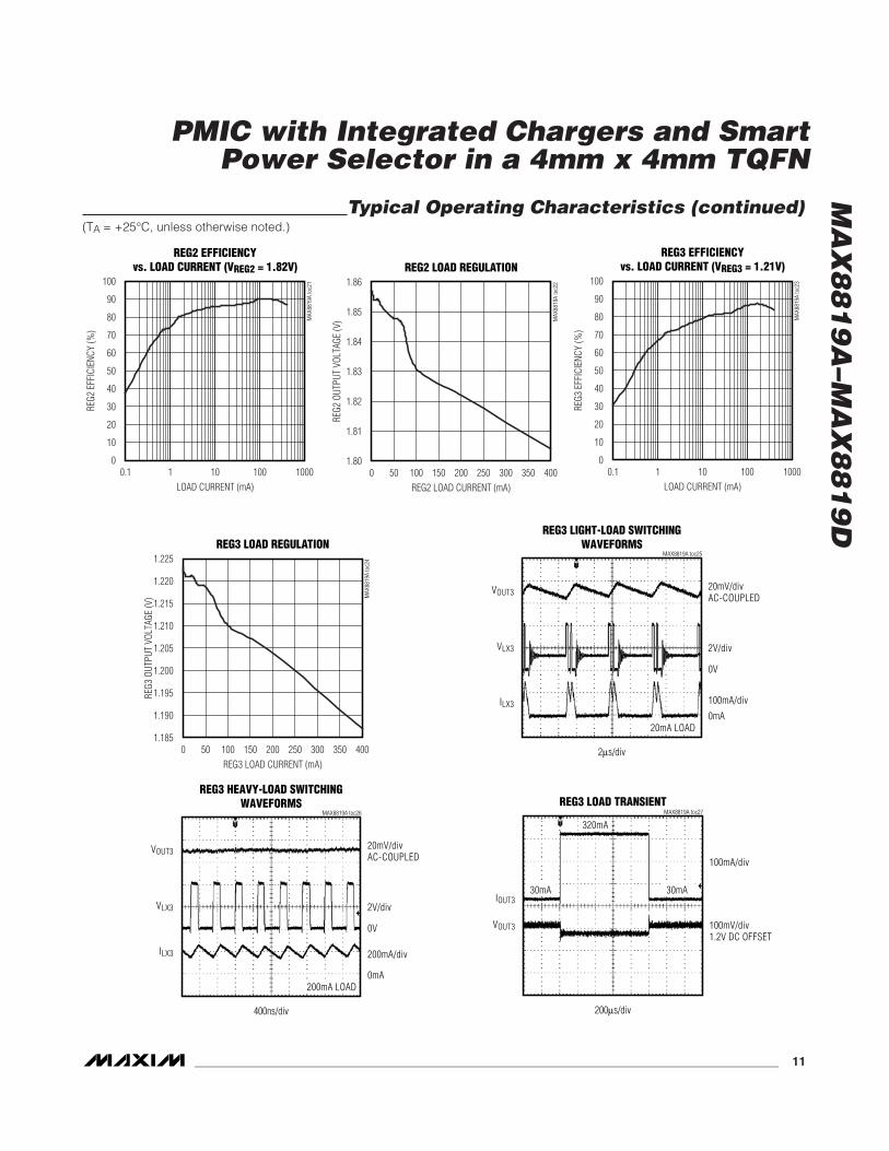
REG2 EFFICIENCYvs. LOAD CURRENT (VREG2 = 1.82V)
LOAD CURRENT (mA)
REG2
EFF
ICIE
NCY
(%)
MAX
8819
A to
c21
0
10
20
30
40
50
60
70
80
90
100
0.1 1 10 100 1000
REG2 LOAD REGULATION
REG2 LOAD CURRENT (mA)
REG2
OUT
PUT
VOLT
AGE
(V) M
AX88
19A
toc2
2
0 50 100 150 200 250 300 350 4001.80
1.81
1.82
1.83
1.84
1.85
1.86
REG3 EFFICIENCYvs. LOAD CURRENT (VREG3 = 1.21V)
LOAD CURRENT (mA)
REG3
EFF
ICIE
NCY
(%)
MAX
8819
A to
c23
0
10
20
30
40
50
60
70
80
90
100
0.1 1 10 100 1000
REG3 LOAD REGULATION
REG3 LOAD CURRENT (mA)
REG3
OUT
PUT
VOLT
AGE
(V) M
AX88
19A
toc2
4
0 50 100 150 200 250 300 350 4001.185
1.190
1.195
1.200
1.205
1.210
1.215
1.220
1.225
REG3 HEAVY-LOAD SWITCHINGWAVEFORMS
MAX8819A toc26
400ns/div
20mV/divAC-COUPLED
2V/div
0V
0mA
200mA/div
VOUT3
VLX3
ILX3
200mA LOAD
REG3 LIGHT-LOAD SWITCHINGWAVEFORMS
MAX8819A toc25
2μs/div
20mV/divAC-COUPLED
2V/div
0V
0mA
100mA/div
VOUT3
VLX3
ILX3
20mA LOAD
REG3 LOAD TRANSIENTMAX8819A toc27
200μs/div
100mA/div
100mV/div1.2V DC OFFSET
30mA 30mA
320mA
IOUT3
VOUT3
MA
X8
81
9A
–MA
X8
81
9D
PMIC with Integrated Chargers and SmartPower Selector in a 4mm x 4mm TQFN
12 ______________________________________________________________________________________
Typical Operating Characteristics (continued)(TA = +25°C, unless otherwise noted.)
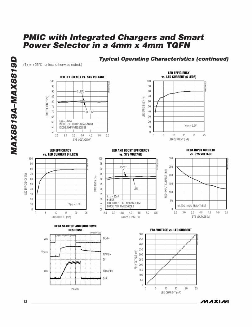
LED EFFICIENCY vs. SYS VOLTAGE
SYS VOLTAGE (V)
LED
EFFI
CIEN
CY (%
)
MAX
8819
A to
c28
2.5 3.0 3.5 4.0 4.5 5.0 5.550
55
60
65
70
75
80
85
90
95
100
6 LEDS
4 LEDS
ILED = 25mAINDUCTOR: TOKO 1096AS-100MDIODE: NXP PMEG3005EB
LED EFFICIENCYvs. LED CURRENT (6 LEDS)
LED CURRENT (mA)LE
D EF
FICI
ENCY
(%)
MAX
8819
A to
c29
0 5 10 15 20 250
10
20
30
40
50
60
70
80
90
100
VSYS = 3.6V
LED EFFICIENCYvs. LED CURRENT (4 LEDS)
LED CURRENT (mA)
LED
EFFI
CIEN
CY (%
)
MAX
8819
A to
c30
0 5 10 15 20 250
10
20
30
40
50
60
70
80
90
100
VSYS = 3.6V
LED AND BOOST EFFICIENCYvs. SYS VOLTAGE
SYS VOLTAGE (V)
EFFI
CIEN
CY (%
)
MAX
8819
A to
c31
2.5 3.0 3.5 4.0 4.5 5.0 5.550
55
60
65
70
75
80
85
90
95
100
ILED = 25mA6 LEDSINDUCTOR: TOKO 1096AS-100MDIODE: NXP PMEG3005EB
BOOST
LED
REG4 INPUT CURRENTvs. SYS VOLTAGE
SYS VOLTAGE (V)
REG4
INPU
T CU
RREN
T (m
A)
MAX
8819
A to
c32
2.5 3.0 3.5 4.0 4.5 5.0 5.50
50
100
150
200
250
300
6 LEDS, 100% BRIGHTNESS
REG4 STARTUP AND SHUTDOWNRESPONSE
MAX8819A toc33
2ms/div
2V/div
10V/div
0V
0mA
10mA/div
VEN
VOVP4
ILED
FB4 VOLTAGE vs. LED CURRENT
LED CURRENT (mA)
FB4
VOLT
AGE
(mV)
MAX
8819
A to
c34
0 5 10 15 20 250
50
100
150
200
250
300
350
400
450
500
MA
X8
81
9A
–MA
X8
81
9D
PMIC with Integrated Chargers and SmartPower Selector in a 4mm x 4mm TQFN
______________________________________________________________________________________ 13
Typical Operating Characteristics (continued)(TA = +25°C, unless otherwise noted.)
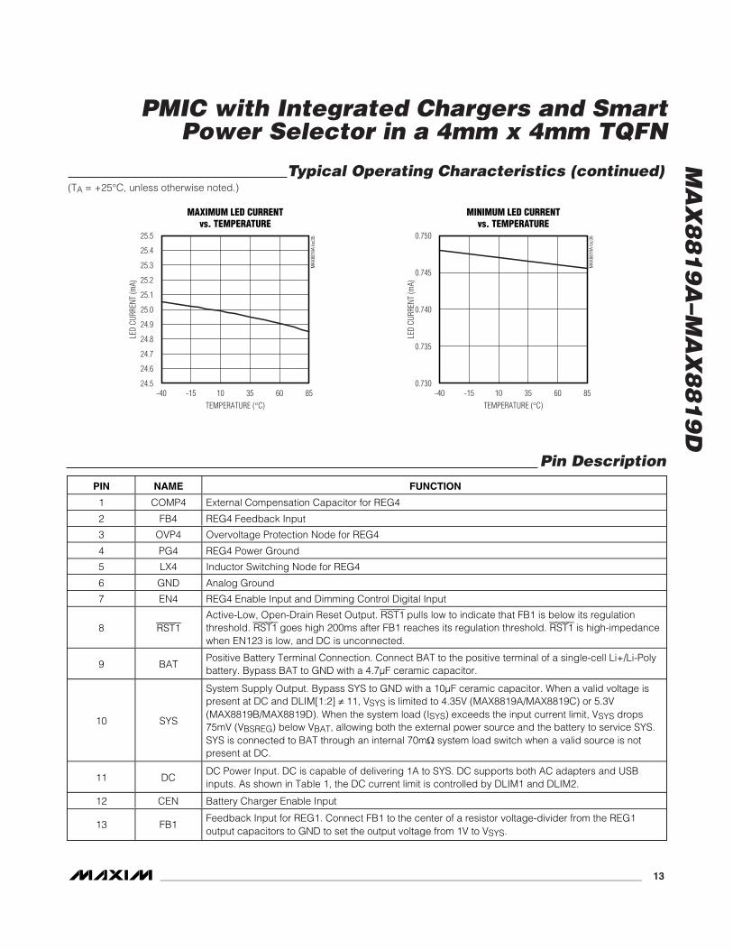
MAXIMUM LED CURRENTvs. TEMPERATURE
TEMPERATURE (°C)
LED
CURR
ENT
(mA)
MAX
8819
A to
c35
-40 -15 10 35 60 8524.5
24.6
24.7
24.8
24.9
25.0
25.1
25.2
25.3
25.4
25.5
MINIMUM LED CURRENTvs. TEMPERATURE
TEMPERATURE (°C)LE
D CU
RREN
T (m
A)
MAX
8819
A to
c36
-40 -15 10 35 60 850.730
0.735
0.740
0.745
0.750
Pin DescriptionPIN NAME FUNCTION
1 COMP4 External Compensation Capacitor for REG4
2 FB4 REG4 Feedback Input
3 OVP4 Overvoltage Protection Node for REG4
4 PG4 REG4 Power Ground
5 LX4 Inductor Switching Node for REG4
6 GND Analog Ground
7 EN4 REG4 Enable Input and Dimming Control Digital Input
8 RST1Active-Low, Open-Drain Reset Output. RST1 pulls low to indicate that FB1 is below its regulationthreshold. RST1 goes high 200ms after FB1 reaches its regulation threshold. RST1 is high-impedancewhen EN123 is low, and DC is unconnected.
9 BATPositive Battery Terminal Connection. Connect BAT to the positive terminal of a single-cell Li+/Li-Polybattery. Bypass BAT to GND with a 4.7μF ceramic capacitor.
10 SYS
System Supply Output. Bypass SYS to GND with a 10μF ceramic capacitor. When a valid voltage ispresent at DC and DLIM[1:2] ≠ 11, VSYS is limited to 4.35V (MAX8819A/MAX8819C) or 5.3V(MAX8819B/MAX8819D). When the system load (ISYS) exceeds the input current limit, VSYS drops75mV (VBSREG) below VBAT, allowing both the external power source and the battery to service SYS.SYS is connected to BAT through an internal 70mΩ system load switch when a valid source is notpresent at DC.
11 DCDC Power Input. DC is capable of delivering 1A to SYS. DC supports both AC adapters and USBinputs. As shown in Table 1, the DC current limit is controlled by DLIM1 and DLIM2.
12 CEN Battery Charger Enable Input
13 FB1Feedback Input for REG1. Connect FB1 to the center of a resistor voltage-divider from the REG1output capacitors to GND to set the output voltage from 1V to VSYS.

MA
X8
81
9A
–MA
X8
81
9D
PMIC with Integrated Chargers and SmartPower Selector in a 4mm x 4mm TQFN
14 ______________________________________________________________________________________
Pin Description (continued)PIN NAME FUNCTION
14 CISETCharge Rate Select Input. Connect a resistor from CISET to GND (RCISET) to set the fast-chargecurrent limit, prequalification-charge current limit, and top-off threshold.
15 CHGActive-Low, Open-Drain Charge Status Output. CHG pulls low to indicate that the battery is charging.See Figure 3 for more information.
16 PG1 REG1 Power Ground
17 LX1Inductor Switching Node for REG1. When enabled, LX1 switches between PV13 and PG1 to regulatethe FB1 voltage to 1.0V. When disabled, LX1 is pulled to PG1 by 1kΩ in shutdown.
18 PV13Power Input for the REG1 and REG3 Converters. Connect PV13 to SYS. Bypass PV13 to PG1 with a4.7μF ceramic capacitor.
19 LX3Inductor Switching Node for REG3. When enabled, LX3 switches between PV13 and PG3 to regulatethe FB3 voltage to 1.0V. When disabled, LX3 is pulled to PG3 by a 1kΩ internal resistor.
20 PG3 REG3 Power Ground
21 DLIM1Input Current-Limit Selection Digital Input 1. Drive high or low according to Table 1 to set the DC inputcurrent limit.
22 FB2Feedback Input for REG2. Connect FB2 to the center of a resistor voltage-divider from the REG2output capacitors to GND to set the output voltage from 1V to VSYS.
23 FB3Feedback Input for REG3. Connect FB3 to the center of a resistor voltage-divider from the REG3output capacitors to GND to set the output voltage from 1V to VSYS.
24 EN123RE G1, RE G2, and RE G3 E nab l e Inp ut. D r i ve E N 123 hi g h to enab l e RE G1, RE G 2, and RE G3. D r i ve E N 123l ow to d i sab l e RE G 1, RE G2, and RE G 3. The enab l e/d i sab l e seq uenci ng i s show n i n Fi g ur es 6 and 7.
25 PV2 Power Input for REG2. Connect PV2 to SYS. Bypass PV2 to PG2 with a 4.7μF ceramic capacitor.
26 LX2Inductor Switching Node for REG2. When enabled, LX2 switches between PV2 and PG2 to regulatethe FB2 voltage to 1.0V. When disabled, LX2 is pulled to PG2 by a 1kΩ internal resistor.
27 PG2 REG2 Power Ground
28 DLIM2Input Current-Limit Selection Digital Input 2. Drive high or low according to Table 1 to set the DC inputcurrent limit.
— EP Exposed Pad

MA
X8
81
9A
–MA
X8
81
9D
PMIC with Integrated Chargers and SmartPower Selector in a 4mm x 4mm TQFN
______________________________________________________________________________________ 15
Detailed DescriptionThe MAX8819_ is a complete power solution thatincludes a battery charger, step-down converters, andWLED power. As shown in Figure 1, the IC integrates aDC power input, Li+/Li-Poly battery charger, three step-down converters, and one step-up converter for powering
white LEDs. All three step-down converters featureadjustable output voltages set with external resistors.
The MAX8819_ has one external power input that con-nects to either an AC-to-DC adapter or USB port. Logicinputs DLIM1 and DLIM2 select the desired input cur-rent limit.
REG1STEP-DOWN
DC-DC
PV13
LX1
FB1
PG1
EN123
BIAS
REG1/RESET87% FALLING
50us BLANKING92% RISING80ms DELAY
ON
OFF
EP
C8*10μF
R8200kΩ
L14.7μH
OUT1
3.0V400mA
R9100kΩ
C74.7μF
SYS
PG1
PG1
PG1
RST1
R10470kΩ
OUT1
RST1
REG2STEP-DOWN
DC-DC
PV2
LX2
FB2
PG2
C10*10μF
R1280.6kΩ
L24.7μH
OUT2
1.8V200mA
R13100kΩ
C94.7μF
SYS
PG2
PG2
PG2
REG3STEP-DOWN
DC-DC
LX3
FB3
PG3
*22μF FOR MAX8819C/MAX8819D IS RECOMMENDED.
C11*10μF
R1420.0kΩ
L34.7μH
OUT3
1.2V300mA
R15100kΩ
PG3 PG3
PULSEDIMMING
AGND
REG4STEP-UPDC-DC
LX4
OVP4
PG4
PG4
FB4
SYS
C30.1μF
50VX7R PG4
EN4
D7
L4 10μH
D1
D2
D3
D4
OUT4
ONOFF
PV13
PV13
EN
EN
EN
PWM
PWM
PWM
UP TO 6WLED
COMP4C4
0.022μF
D5
R120
(25mA)
PG4
D6
C20.1μF
SMARTPOWER
SELECTOR
Li+/Li-PolyBATTERY
CHARGER ANDSYSTEM LOAD
SWITCH
DLIM1 DLIM2
GLITCH FILTER
C14.7μF
AC-TO-DCADAPTER
SYS
BAT
CISET
C510μF
SYS
C64.7μF
R2 OUT1
CHG
R6470kΩ
CHG
ON
OFF
Li+/LiPoBATTERY
CEN
DLIM1
DLIM2
DCBATTERY
CAPACITY(mAh)
DESIREDCHARGERATE (C)
FAST-CHARGE
CURRENT(mA)
300 14.3 210400
0.70.70.70.70.7
10.7 280600 7.15 420800 5.36 560900 4.75 632
0 0 10000 1 475
01 951 1 SUSPEND
DC ILIM (mA)
R7 (kΩ)
+
MAX8819AMAX8819B MAX8819C MAX8819D
Figure 1. Functional Diagram/Typical Applications Circuit

MA
X8
81
9A
–MA
X8
81
9D
PMIC with Integrated Chargers and SmartPower Selector in a 4mm x 4mm TQFN
16 ______________________________________________________________________________________
In addition to charging the battery, the IC suppliespower to the system through the SYS output. Thecharging current is provided from SYS so that the setinput current limit controls the total SYS current, this isthe sum of the system load current and the battery-charging current.
In some instances, there may not be enough DC inputcurrent to supply peak system loads. The Smart PowerSelector circuitry offers flexible power distribution froman AC-to-DC adapter or USB source to the battery andsystem load. The battery is charged with any availablepower not used by the system load. If a system loadpeak exceeds the input current limit, supplemental cur-rent is taken from the battery. Thermal limiting preventsoverheating by reducing power drawn from the inputsource. In the past, it might have been necessary toreduce system functionality to limit current drain when aUSB source is connected. However, with theMAX8819_, this is no longer the case. When the DC orUSB source hits its limit, the battery supplies supple-mental current to maintain the load.
The IC features overvoltage protection. Part of this protec-tion is a 4.35V (MAX8819A/MAX8819C) or 5.3V(MAX8819B/MAX8819D) voltage limiter at SYS. If DCexceeds the overvoltage threshold of 5.88V (VOVLO_DC),the input limiter disconnects SYS from DC, but battery-powered operation of all regulators is still allowed.
Input LimiterThe Smart Power Selector seamlessly distributes powerbetween the current-limited external input (DC), the bat-tery (BAT), and the system load (SYS). The basic func-tions performed are:
With both an external power supply (DC) and battery(BAT) connected:
• When the system load requirements are less thanthe input current limit, the battery is charged withresidual power from the input.
• When the system load requirements exceed theinput current limit, the battery supplies supple-mental current to the load through the internal sys-tem load switch.
• When the battery is connected and there is noexternal power input, the system (SYS) is poweredfrom the battery.
• When an external power input is connected andthere is no battery, the system (SYS) is poweredfrom the external power input.
A thermal-limiting circuit reduces the battery chargerate and external power source current to prevent theMAX8819_ from overheating.
System Load SwitchAn internal 70mΩ MOSFET connects SYS to BAT whenno voltage source is available at DC. When an externalsource is detected at DC, this switch opens and SYS ispowered from the valid input source through the SmartPower Selector.
When the system load requirements exceed the inputcurrent limit, the battery supplies supplemental currentto the load through the internal system load switch. Ifthe system load continuously exceeds the input currentlimit, the battery does not charge, even though externalpower is connected. This is not expected to occur inmost cases because high loads usually occur only inshort peaks. During these peaks, battery energy isused, but at all other times the battery charges.
DC Power Input (DC, DLIM1, DLIM2)DC is a current-limited power input that supplies thesystem (SYS) up to 1A. The DC to SYS switch is a linearregulator designed to operate in dropout. This linearregulator prevents the SYS voltage from exceeding5.3V for the MAX8819B/MAX8819D or 4.35V for theMAX8819A/MAX8819C. As shown in Table 1, DC sup-ports four different current limits that are set with theDLIM1 and DLIM2 digital inputs. These current limitsare ideally suited for use with AC-to-DC wall adaptersand USB power. The operating voltage range for DC is4.1V to 5.5V, but it can tolerate up to 6V without dam-age. When the DC input voltage is below the undervolt-age threshold (4V), it is considered invalid. When theDC voltage is below the battery voltage it is consideredinvalid. The DC power input is disconnected when theDC voltage is invalid. Bypass DC to ground with at leasta 4.7μF capacitor.
Four current settings are provided based upon the set-tings of DLIM1 and DLIM2, see Table 1. DLIM1 andDLIM2 are deglitched. This deglitching prevents theproblem of major carry transitions momentarily enteringthe suspend state.
DLIM1 DLIM2 DC ILIM (mA)
0 0 1000
0 1 475
1 0 95
1 1 Suspend
Table 1. DC Current-Limit Settings

MA
X8
81
9A
–MA
X8
81
9D
PMIC with Integrated Chargers and SmartPower Selector in a 4mm x 4mm TQFN
______________________________________________________________________________________ 17
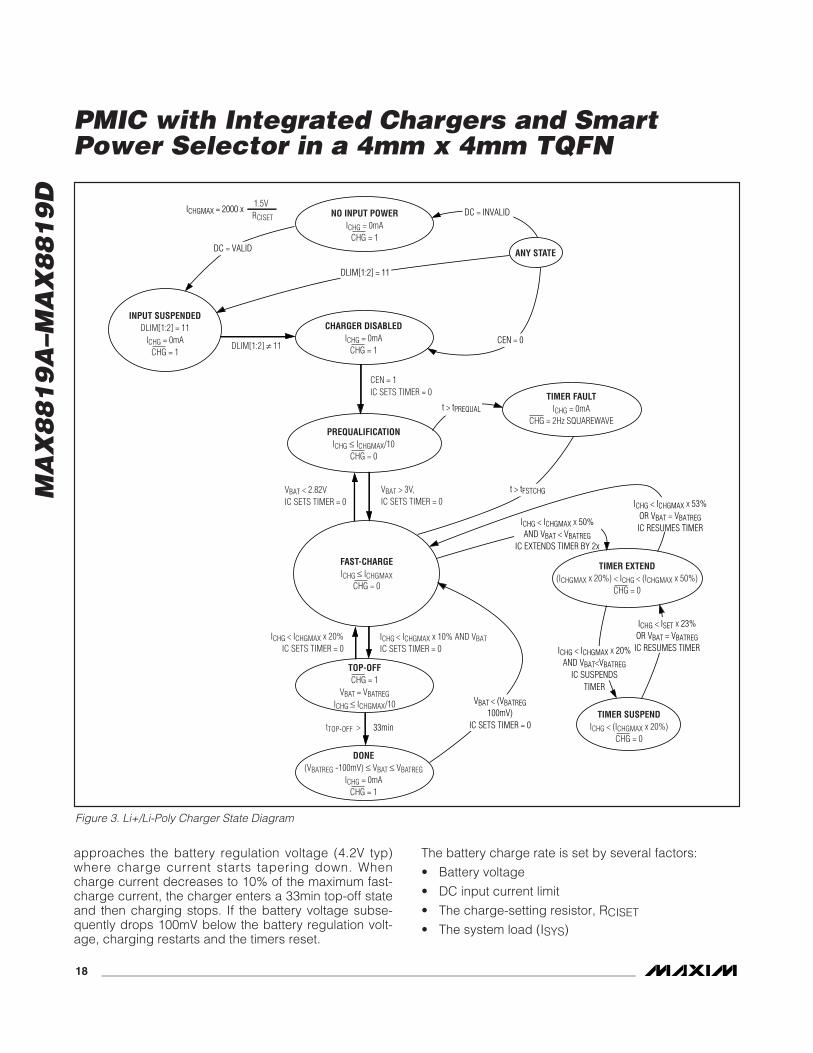
Battery ChargerFigure 2 shows the typical Li+/Li-Poly charge profile forthe MAX8819_, and Figure 3 shows the battery chargerstate diagram.
With a valid DC input that is not suspended, the batterycharger initiates a charge cycle once CEN is drivenhigh. It first detects the battery voltage. If the battery
voltage is less than the prequalification threshold(3.0V), the charger enters prequalification mode andcharges the battery at 10% of the maximum fast-chargecurrent while deeply discharged. Once the battery volt-age rises to 3.0V, the charger transitions to fast-chargemode and applies the maximum charge current. Ascharging continues, the battery voltage rises until it
VBATPRQ
VBATREG
ICHGMAX
IPQ
ITO
0
PREQUALIFICATION FAST-CHARGE(CONSTANT CURRENT)
TOP-OFF
FAST-CHARGE(CONSTANT VOLTAGE)
DONE
LOW
HIGHIMPEDANCE
BATT
ERY
VOLT
AGE
BATT
ERY
CHAR
GE C
URRE
NTCH
G
Figure 2. Li+/Li-Poly Charge Profile
MA
X8
81
9A
–MA
X8
81
9D
PMIC with Integrated Chargers and SmartPower Selector in a 4mm x 4mm TQFN
18 ______________________________________________________________________________________
approaches the battery regulation voltage (4.2V typ)where charge current starts tapering down. Whencharge current decreases to 10% of the maximum fast-charge current, the charger enters a 33min top-off stateand then charging stops. If the battery voltage subse-quently drops 100mV below the battery regulation volt-age, charging restarts and the timers reset.
The battery charge rate is set by several factors:
• Battery voltage
• DC input current limit
• The charge-setting resistor, RCISET
• The system load (ISYS)
ANY STATE
VBAT > 3V,IC SETS TIMER = 0
VBAT < 2.82VIC SETS TIMER = 0
DLIM[1:2] ≠ 11
CEN = 1IC SETS TIMER = 0
CHARGER DISABLEDICHG = 0mA
CHG = 1
DONE(VBATREG -100mV) ≤ VBAT ≤ VBATREG
ICHG = 0mACHG = 1
TOP-OFFCHG = 1
VBAT = VBATREGICHG ≤ ICHGMAX/10
TIMER SUSPENDICHG < (ICHGMAX x 20%)
CHG = 0
FAST-CHARGEICHG ≤ ICHGMAX
CHG = 0
PREQUALIFICATIONICHG ≤ ICHGMAX/10
CHG = 0
TIMER FAULTICHG = 0mA
CHG = 2Hz SQUAREWAVE
TIMER EXTEND(ICHGMAX x 20%) < ICHG < (ICHGMAX x 50%)
CHG = 0
NO INPUT POWERICHG = 0mA
CHG = 1
INPUT SUSPENDEDDLIM[1:2] = 11
ICHG = 0mACHG = 1
DC = INVALID
DLIM[1:2] = 11
DC = VALID
CEN = 0
t > tPREQUAL
t > tFSTCHG
ICHG < ICHGMAX x 53%OR VBAT = VBATREGIC RESUMES TIMER
ICHG < ICHGMAX x 50%AND VBAT < VBATREG
IC EXTENDS TIMER BY 2x
ICHG < ISET x 23%OR VBAT = VBATREGIC RESUMES TIMERICHG < ICHGMAX x 20%
AND VBAT<VBATREGIC SUSPENDS
TIMERVBAT < (VBATREG
100mV)IC SETS TIMER = 0
ICHG < ICHGMAX x 10% AND VBATIC SETS TIMER = 0
tTOP-OFF >
ICHG < ICHGMAX x 20%IC SETS TIMER = 0
ICHGMAX = 2000 x 1.5VRCISET
33min
Figure 3. Li+/Li-Poly Charger State Diagram

MA
X8
81
9A
–MA
X8
81
9D
PMIC with Integrated Chargers and SmartPower Selector in a 4mm x 4mm TQFN
______________________________________________________________________________________ 19
• The die temperature
• The battery charger is enabled by the processor dri-ving the CEN input high. A valid input must be avail-able at DC. The battery charger is disabled withouta valid input at DC or by driving CEN low.
• The system current has priority over the batterycharger; the battery charger automatically reducesits charge current to maintain the input current limitwhile still providing the system current (ISYS).
• The input current limit is tapered down from full cur-rent to zero current when the die temperature transi-tions from +100°C to +120°C. Since ISYS has priorityover the battery charge current, the battery chargecurrent tapers down before ISYS. The overall result isself-regulation of die temperature (see the ThermalLimiting and Overload Protection section for moreinformation).
• The battery charger stops charging in done modeas shown in Figures 2 and 3.
Charge Status Output (CHG)CHG is an open-drain, active-low output that indicatescharger status. As shown in Figures 2 and 3, CHG islow when the charger is in its prequalification or fast-charge states. When a timer count is exceeded ineither state, CHG indicates the fault by blinking at a2Hz rate and remains in that state until the charger isreset by CEN going low, removal of DC or settingDLIM[1:2] = 11.
When the MAX8819_ is used with a microprocessor(μP), connect a pullup resistor between CHG and thesystem logic voltage to indicate charge status to theμP. Alternatively, CHG sinks up to 20mA for an LEDcharge indicator.
If the charge status output feature is not required, con-nect CHG to ground or leave unconnected.
Charge TimerAs shown in Figure 3, a fault timer prevents the batteryfrom charging indefinitely. In prequalification mode, thecharge time is internally fixed to 33min.
tPREQUAL = 33min
In fast-charge mode, the charge timer is internally fixedto 660min.
tFSTCHG = 660min
When the charger exits fast-charge mode, a fixed33min top-off mode is entered:
tTOP-OFF = 33min
While in the constant-current fast-charge mode (Figure2), if the MAX8819_ reduces the battery charge current
due to its internal die temperature or large systemloads, it slows down the charge timer. This feature elim-inates nuisance charge timer faults. When the batterycharge current is between 100% and 50% of its pro-grammed fast-charge level, the fast-charge timer runsat full speed. When the battery charge current isbetween 50% and 20% programmed fast-charge level,the fast-charge timer is slowed by 2x. Similarly, whenthe battery charge current is below 20% of the pro-grammed fast-charge level, the fast-charge timer is
FAST-CHARGE, PREQUALIFICATION, AND TOP-OFFCURRENT vs. CHARGE-SETTING RESISTOR
RCISET (kΩ)
CURR
ENT
(mA)
0 5 10 15 201
10
100
1000
10,000
IPREQUAL, ITOP-OFF
ICHGMAX
Figure 4. Calculated Charge Currents vs. RCISET
RCISET (kΩ)ICHGMAX
(mA)IPQ (mA) ITO (mA)
3.01 1000 100 100
4.02 746 75 75
4.99 601 60 60
6.04 497 50 50
6.98 430 43 43
8.06 372 37 37
9.09 330 33 33
10 300 30 30
11 273 27 27
12.1 248 25 25
13 231 23 23
14 214 21 21
15 200 20 20
Table 2. Calculated Charge Currents vs.RCISET

MA
X8
81
9A
–MA
X8
81
9D
PMIC with Integrated Chargers and SmartPower Selector in a 4mm x 4mm TQFN
20 ______________________________________________________________________________________
paused. The fast-charge timer is not slowed or pausedwhen the charger is in the constant voltage portion ofits fast-charge mode (Figure 2) where the charge cur-rent reduces normally.
Charge Current (CISET)As shown in Table 2 and Figure 4, a resistor from CISETto ground (RCISET) sets the maximum fast-charge cur-rent (ICHGMAX), the charge current in prequalificationmode (IPREQUAL), and the top-off threshold (ITOP-OFF).The MAX8819_ supports values of ICHGMAX from 200mAto 1000mA. Select the RCISET as follows:
Determine ICHGMAX by considering the characteristicsof the battery. It is not necessary to limit the charge cur-rent based on the capabilities of the expected AC-to-DC adapter or USB/DC input current limit, the systemload, or thermal limitations of the PCB. The IC automati-cally lowers the charging current as necessary toaccommodate for these factors.
For the selected value of RCISET, calculate ICHGMAX,IPREQUAL, and ITOP-OFF as follows:
Step-Down Converters(REG1, REG2, REG3)
REG1, REG2, and REG3 are high-efficiency, 2MHz cur-rent-mode step-down converters with adjustable outputs.REG1 is designed to deliver 400mA for the MAX8819A/MAX8819B and 550mA for the MAX8819C/MAX8819D.REG2 and REG3 are designed to deliver 300mA for theMAX8819A/MAX8819B and 500mA for the MAX8819C/MAX8819D.
The step-down regulator power inputs (PV_) must beconnected to SYS. The step-down regulators operatewith VSYS from 2.6V to 5.5V. Undervoltage lockoutensures that the step-down regulators do not operatewith SYS below 2.55V (max).
See the Step-Down Converter Enable/Disable (EN123)and Sequencing section for how to enable and disablethe step-down converters. When enabled, theMAX8819_ gradually ramps each output up during a2.6ms soft-start time. When enabled, the MAX8819C/MAX8819D sequentially ramps up each output. Soft-start eliminates input current surges when regulatorsare enabled.
See the Step-Down Control Scheme section for informa-tion about the step-down converters control scheme.
The IC uses external resistor-dividers to set the step-down output voltages between 1V and VSYS. Use atleast 10μA of bias current in these dividers to ensure nochange in the stability of the closed-loop system. To setthe output voltage, select a value for the resistor con-nected between FB_ and GND (RFBL). The recom-mended value is 100kΩ. Next, calculate the value of theresistor connected from FB_ to the output (RFBH):
REG1, REG2, and REG3 are optimized for high, medi-um, and low output voltages, respectively. The highestoverall efficiency occurs with V1 set to the highest out-put voltage and V3 set to the lowest output voltage.
REG2 can be disabled by connecting PV2 to GND.
Step-Down Control SchemeAt light load, the step-down converter switches only asneeded to supply the load. This improves light-load effi-ciency. At higher load currents (~80mA), the step-downconverter transitions to fixed 2MHz switching.
Step-Down Dropout and Minimum Duty CycleAll of the step-down regulators are capable of operat-ing in 100% duty-cycle dropout, however, REG1 hasbeen optimized for this mode of operation. During100% duty-cycle operation, the high-side p-channelMOSFET turns on constantly, connecting the input tothe output through the inductor. The dropout voltage(VDO) is calculated as follows:
where:
RP = p-channel power switch RDS(ON)RLSR = external inductor ESR
The minimum duty cycle for all step-down regulators is12.5% (typ), allowing a regulation voltage as low as 1Vover the full SYS operating range. REG3 is optimizedfor low duty-cycle operation.
Step-Down Input CapacitorThe input capacitor in a step-down converter reducescurrent peaks drawn from the power source andreduces switching noise in the controller. The imped-ance of the input capacitor at the switching frequencymust be less than that of the source impedance of the
V I R RDO LOAD P L= +( )
R RV
VFBH FBLOUT= × −⎛
⎝⎜⎞⎠⎟1 0
1.
IV
R
I I
CHGMAXCISET
PREQUAL TOP OFF
= ×
= =−
20001 5
10
.
%% × ICHGMAX
RV
ICISETCHGMAX
= ×20001 5.
MA
X8
81
9A
–MA
X8
81
9D
PMIC with Integrated Chargers and SmartPower Selector in a 4mm x 4mm TQFN
______________________________________________________________________________________ 21
supply so that high-frequency switching currents do notpass through the input source.
The step-down regulator power inputs are critical dis-continuous current paths that require careful bypass-ing. In the PCB layout, place the step-down converterinput bypass capacitors as close as possible to eachpair of switching converter power input pins (PV_ toPG_) to minimize parasitic inductance. If making con-nections to these capacitors through vias, be sure touse multiple vias to ensure that the layout does notinsert excess inductance or resistance between thebypass capacitor and the power pins.
The input capacitor must meet the input ripple currentrequirement imposed by the step-down converter.Ceramic capacitors are preferred due to their low ESRand resilience to power-up surge currents. Choose theinput capacitor so that its temperature rise due to inputripple-current does not exceed approximately +10°C.For a step-down DC-DC converter, the maximum inputripple current is half of the output current. This maxi-mum input ripple current occurs when the step-downconverter operates at 50% duty factor (VIN = 2 x VOUT).
Bypass each step-down converter input with a 4.7μFceramic capacitor from PV_ to PG_. Use capacitors thatmaintain their capacitance over temperature and DCbias. Ceramic capacitors with an X7R or X5R tempera-ture characteristic generally perform well. The capacitorvoltage rating should be 6.3V or greater.
Step-Down Output CapacitorsThe output capacitance keeps output ripple small andensures control-loop stability. The output capacitormust have low impedance at the switching frequency.Ceramic, polymer, and tantalum capacitors are suitablewith ceramic exhibiting the lowest ESR and lowest high-frequency impedance. The MAX8819A/MAX8819Brequire at least 10μF of output capacitance. TheMAX8819C/MAX8819D require ar least 22μF of outputcapacitance.
As the case sizes of ceramic surface-mount capacitorsdecreases, their capacitance vs. DC bias voltage char-acteristic becomes poor. Due to this characteristic, it ispossible for 0805 capacitors to perform well while 0603capacitors of the same value may not. The MAX8819A/MAX8819B require a nominal output capacitance of10μF, however, after their DC bias voltage derating, theoutput capacitance must be at least 7.5μF.
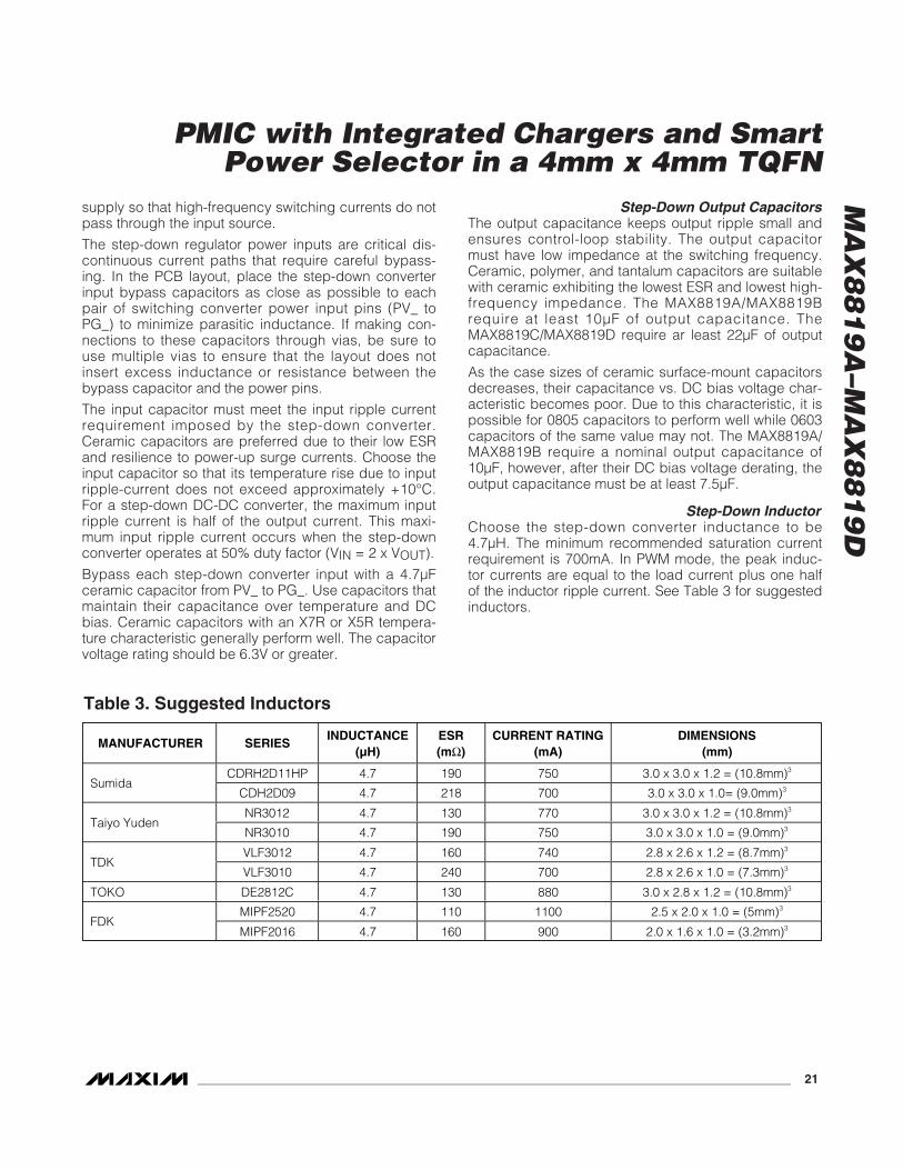
Step-Down InductorChoose the step-down converter inductance to be4.7μH. The minimum recommended saturation currentrequirement is 700mA. In PWM mode, the peak induc-tor currents are equal to the load current plus one halfof the inductor ripple current. See Table 3 for suggestedinductors.
MANUFACTURER SERIESINDUCTANCE
(µH)ESR(mΩ)
CURRENT RATING(mA)
DIMENSIONS(mm)
CDRH2D11HP 4.7 190 750 3.0 x 3.0 x 1.2 = (10.8mm)3
SumidaCDH2D09 4.7 218 700 3.0 x 3.0 x 1.0= (9.0mm)3
NR3012 4.7 130 770 3.0 x 3.0 x 1.2 = (10.8mm)3
Taiyo YudenNR3010 4.7 190 750 3.0 x 3.0 x 1.0 = (9.0mm)3
VLF3012 4.7 160 740 2.8 x 2.6 x 1.2 = (8.7mm)3
TDKVLF3010 4.7 240 700 2.8 x 2.6 x 1.0 = (7.3mm)3
TOKO DE2812C 4.7 130 880 3.0 x 2.8 x 1.2 = (10.8mm)3
MIPF2520 4.7 110 1100 2.5 x 2.0 x 1.0 = (5mm)3
FDKMIPF2016 4.7 160 900 2.0 x 1.6 x 1.0 = (3.2mm)3
Table 3. Suggested Inductors

MA
X8
81
9A
–MA
X8
81
9D
PMIC with Integrated Chargers and SmartPower Selector in a 4mm x 4mm TQFN
22 ______________________________________________________________________________________
The peak-to-peak inductor ripple current during PWMoperation is calculated as follows:
where fS is the 2MHz switching frequency.
The peak inductor current during PWM operation is cal-culated as follows:
Step-Down Converter Maximum Output CurrentThe maximum regulated output current from a step-downconverter is ultimately determined by the p-channel peakcurrent limit (IPK). The calculation follows:
IOUT,MAX = IPK – (IP-P/2)
For example, if VSYS = 5.3V, VOUT = 3V, fS = 2MHz,L = 4.7μH, and IPK = 0.6A:
IP-P = 3V x (5.3V - 3V)/(5.3V x 2MHz x 4.7μH) = 0.138A
then IOUT_MAX = 0.6A - (0.138A/2) = 0.531A.
I II
L PEAK LOADP P
_ = + −2
IV V V
V f LP POUT SYS OUT
SYS S− = −
× ×( )
+
-
+
-
+
-
+
-
6.0V RISING400mV HYST.
4.0V RISING500mV HYST.
SOFT-STARTREG2
EN OK REG1OK
SOFT-STARTREG1
EN OK REG2OK
SOFT-STARTREG3
EN OK REG3OK
2.5V RISING100mV HYST.
2MHzOSC
BIASANDREF
64 CYCLEDELAY(32μs)
+165°C
DIE TEMP
SYS
DC
EN4
DCPOK
READY
READYREGON
DCOVLO
DCUVLO
SYSOK
DT165
SOFT-STARTREG4
EN OK REG4OK
EN123
REGON
MAX8819AMAX8819B
Figure 5a. MAX8819A/MAX8819B Enable/Disable Logic

MA
X8
81
9A
–MA
X8
81
9D
PMIC with Integrated Chargers and SmartPower Selector in a 4mm x 4mm TQFN
______________________________________________________________________________________ 23
As the load current is increased beyond this point, theoutput voltage sags and the converter goes out of regu-lation because the inductor current cannot increaseabove the p-channel peak current limit.
Step-Down Converter Short-Circuit ProtectionThe step-down converter implements short-circuit protec-tion by monitoring the feedback voltage, VFB_. After soft-start, if VFB_ drops below 0.23V, the converter reduces itsswitching frequency to fS/3. The inductor current stillreaches the p-channel peak current limit, however, atone-third the frequency. Therefore, the output and inputcurrents are reduced to approximately one-third of themaximum value in response to an output short circuit to
ground. When the short is removed, the inductor currentraises the voltage on the output capacitor and the step-down converter resumes normal operation.
REG1 Reset (RST1)RST1 is an active-low, open-drain output that pulls lowto indicate that FB1 is below its regulation threshold.RST1 goes high 200ms after FB1 reaches its regulationthreshold. RST1 is high-impedance when EN123 ishigh. See Figures 6 and 7.
A 50μs blanking delay is provided when FB1 is falling,so that RST1 does not glitch if the REG1 output voltageis dynamically adjusted by altering the resistors in itsfeedback network.
+
-
+
-
+
-
+
-
6.0V RISING400mV HYST.
4.0V RISING500mV HYST.
SOFT-STARTREG2
EN OK REG1OK
SOFT-STARTREG1
EN OK REG2OK
SOFT-STARTREG3
EN OK REG3OK
2.5V RISING100mV HYST.
2MHzOSC
BIASANDREF
64 CYCLEDELAY(32μs)
+165°C
DIE TEMP
SYS
DC
EN4
DCPOK
READY
READYREGON
DCOVLO
DCUVLO
SYSOK
DT165
SOFT-STARTREG4
EN OK REG4OK
EN123
REGON
MAX8819CMAX8819D
Figure 5b. MAX8819C/MAX8819D Enable Logic
MA
X8
81
9A
–MA
X8
81
9D
PMIC with Integrated Chargers and SmartPower Selector in a 4mm x 4mm TQFN
24 ______________________________________________________________________________________
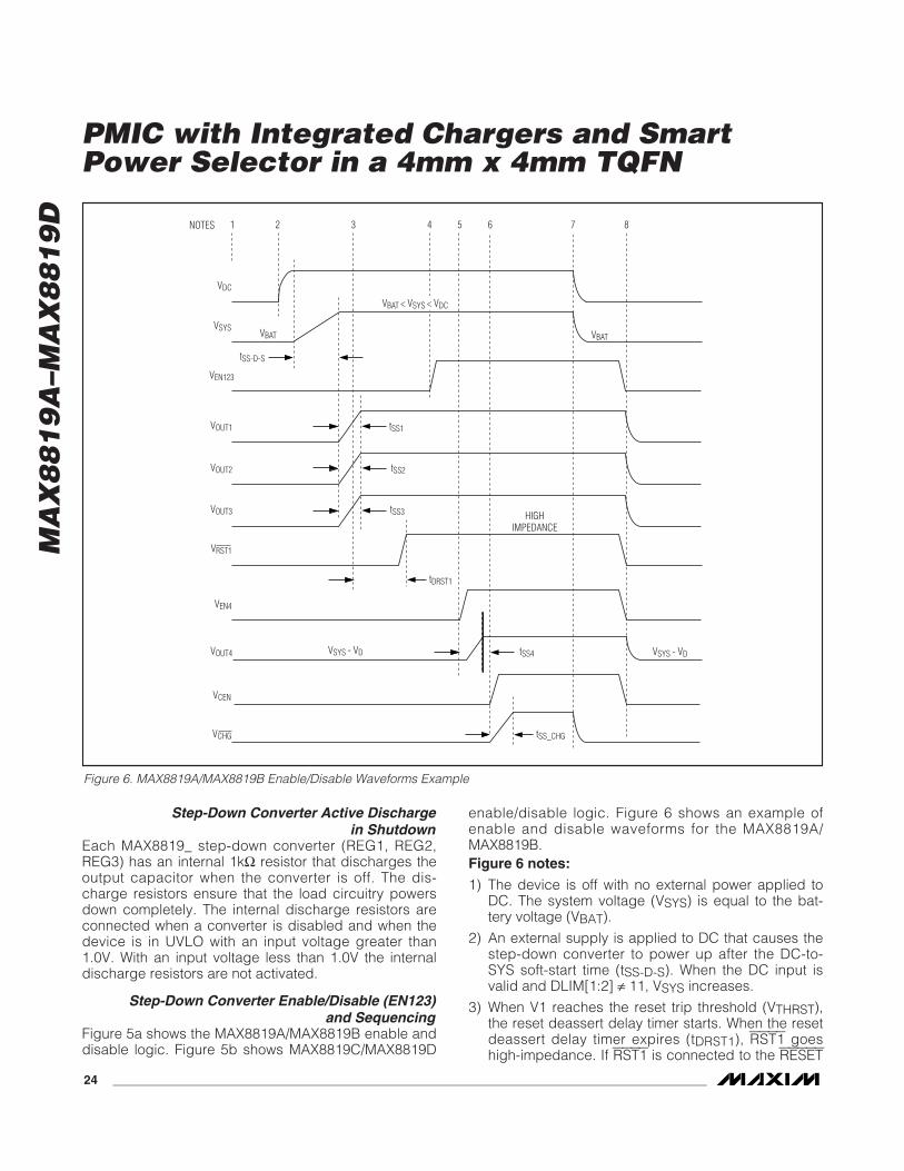
Step-Down Converter Active Dischargein Shutdown
Each MAX8819_ step-down converter (REG1, REG2,REG3) has an internal 1kΩ resistor that discharges theoutput capacitor when the converter is off. The dis-charge resistors ensure that the load circuitry powersdown completely. The internal discharge resistors areconnected when a converter is disabled and when thedevice is in UVLO with an input voltage greater than1.0V. With an input voltage less than 1.0V the internaldischarge resistors are not activated.
Step-Down Converter Enable/Disable (EN123)and Sequencing
Figure 5a shows the MAX8819A/MAX8819B enable anddisable logic. Figure 5b shows MAX8819C/MAX8819D
enable/disable logic. Figure 6 shows an example ofenable and disable waveforms for the MAX8819A/MAX8819B.Figure 6 notes:
1) The device is off with no external power applied toDC. The system voltage (VSYS) is equal to the bat-tery voltage (VBAT).
2) An external supply is applied to DC that causes thestep-down converter to power up after the DC-to-SYS soft-start time (tSS-D-S). When the DC input isvalid and DLIM[1:2] ≠ 11, VSYS increases.
3) When V1 reaches the reset trip threshold (VTHRST),the reset deassert delay timer starts. When the resetdeassert delay timer expires (tDRST1), RST1 goeshigh-impedance. If RST1 is connected to the RESET
VEN123
VOUT1
VOUT2
VOUT3
VDC
tSS-D-S
VSYS
VSYS - VD
VBAT
HIGHIMPEDANCE
tSS1
NOTES 1 2
tSS2
tSS3
VRST1
tDRST1
3 4
VEN4
5
tSS4VOUT4
VBAT
7 8
tSS_CHG
6
VSYS - VD
VCEN
VCHG
VBAT < VSYS < VDC
Figure 6. MAX8819A/MAX8819B Enable/Disable Waveforms Example

MA
X8
81
9A
–MA
X8
81
9D
PMIC with Integrated Chargers and SmartPower Selector in a 4mm x 4mm TQFN
______________________________________________________________________________________ 25
input of the system μP, the processor can begin itsboot-up sequence up at this time.
4) During the μP’s boot-up sequence, it asserts EN123to keep the step-down converters enabled, even ifDC is removed.
5) After the μP has booted, it asserts EN4 to turn on thedisplay’s backlight.
6) CEN is asserted by the μP to start a charge cycle.
7) The external supply is removed from DC and VSYSfalls. The converters remain enabled because the μPhas asserted EN123 and EN4, but the battery charg-ing current drops to zero even though CEN is stillasserted. CHG goes high impedance.
8) System is turned off by deasserting EN123, EN4, andCEN; RST1 goes low to reset the μP.
Figure 7 notes:1) The MAX8819C/MAX8819D are off with no external
power applied to DC. The system voltage (VSYS) isequal to the battery voltage (VBAT).
2) An external supply is applied to DC that causes thestep-down regulator to power up after the DC-to-SYS soft-start time (tSS-D-S). When the DC input isvalid and DC is not suspended, VSYS rises.
3) EN123 is pulled high to start the OUT3, OUT2, andOUT1 power-up sequence. When OUT1 reaches thereset trip threshold (VTHRST), the reset deassertdelay timer starts. When the reset deassert delaytimer expires (tDRST1 200ms typ.), RST1 goes high-impedance. If RST1 is connected to the RESET inputof the system μP, the processor can begin its boot-up sequence at this time.
VEN123
VOUT3
VOUT2
VOUT1
VDC
tSS-D-S
VSYS
VSYS - VD
VBAT
2.6ms
NOTES 1 2
2.6ms
2.6ms
VRST1
3 4
VEN4
5
tSS4VOUT4
VBAT
7
tSS_CHG
6
VSYS - VD
VCEN
VCHG
VBAT < VSYS < VDC
200ms
HIGH IMPEDANCE
Figure 7. MAX8819C/MAX8819D Enable/Disable Waveforms Example
MA
X8
81
9A
–MA
X8
81
9D
PMIC with Integrated Chargers and SmartPower Selector in a 4mm x 4mm TQFN
26 ______________________________________________________________________________________
4) EN4 to turn on the display’s backlight.
5) CEN is asserted by the μP to start a charge cycle.
6) The external supply is removed from DC and VSYSfalls. The regulators remain enabled because EN123and EN4 are asserted, but the battery charging cur-rent drops to zero even though CEN is still asserted.CHG goes high-impedance.
7) System is turned off by deasserting EN123, EN4,and CEN. OUT1, OUT2, and OUT3 power down inthe opposite order of power-up. RST1 goes low toreset the μP.
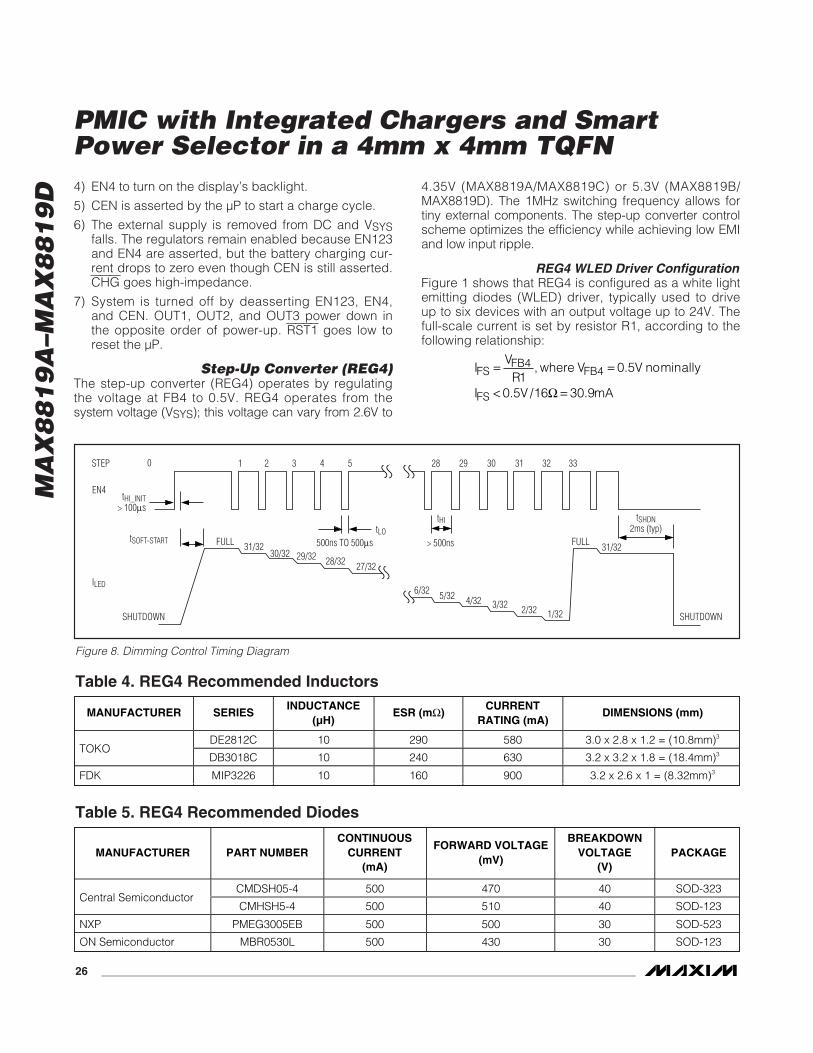
Step-Up Converter (REG4)The step-up converter (REG4) operates by regulatingthe voltage at FB4 to 0.5V. REG4 operates from thesystem voltage (VSYS); this voltage can vary from 2.6V to
4.35V (MAX8819A/MAX8819C) or 5.3V (MAX8819B/MAX8819D). The 1MHz switching frequency allows fortiny external components. The step-up converter controlscheme optimizes the efficiency while achieving low EMIand low input ripple.
REG4 WLED Driver ConfigurationFigure 1 shows that REG4 is configured as a white lightemitting diodes (WLED) driver, typically used to driveup to six devices with an output voltage up to 24V. Thefull-scale current is set by resistor R1, according to thefollowing relationship:
IV
Rwhere V V no ally
I V mA
FSFB
FB
FS
= =
< =
441
0 5
0 5 16 30 9
, . min
. / .Ω
EN4
ILED
SHUTDOWN
FULL 31/3230/32 29/32 28/32 27/32
5/32 4/32 3/32 2/32 1/32
FULL 31/32
1 3332313029285432
tLO
tHI tSHDN2ms (typ)
> 500ns
0
tSOFT-START
6/32
tHI_INIT> 100μs
SHUTDOWN
STEP
500ns TO 500μs
Figure 8. Dimming Control Timing Diagram
MANUFACTURER SERIESINDUCTANCE
(µH)ESR (mΩ)
CURRENTRATING (mA)
DIMENSIONS (mm)
DE2812C 10 290 580 3.0 x 2.8 x 1.2 = (10.8mm)3
TOKODB3018C 10 240 630 3.2 x 3.2 x 1.8 = (18.4mm)3
FDK MIP3226 10 160 900 3.2 x 2.6 x 1 = (8.32mm)3
Table 4. REG4 Recommended Inductors
MANUFACTURER PART NUMBERCONTINUOUS
CURRENT(mA)
FORWARD VOLTAGE(mV)
BREAKDOWNVOLTAGE
(V)PACKAGE
CMDSH05-4 500 470 40 SOD-323Central Semiconductor
CMHSH5-4 500 510 40 SOD-123
NXP PMEG3005EB 500 500 30 SOD-523
ON Semiconductor MBR0530L 500 430 30 SOD-123
Table 5. REG4 Recommended Diodes

MA
X8
81
9A
–MA
X8
81
9D
PMIC with Integrated Chargers and SmartPower Selector in a 4mm x 4mm TQFN
______________________________________________________________________________________ 27
EN4 enables REG4, disables REG4, and adjusts the volt-age on FB4 in 32 linear steps. If current adjustment is notrequired, EN4 acts as a simple enable/disable controller.Driving EN4 high for at least 100μs powers up REG4 andsets VFB4 to 0.5V. Pulling EN4 low for at least 2ms dis-ables REG4. To adjust VFB4, apply pulses as shown inFigure 8. Dim the WLEDs by pulsing EN4 low (500ns to500μs pulse width). Each pulse reduces the LED currentby 1/32. Note: When REG4 is disabled, OUT4 is equal toVSYS minus the drop from the catch diode.
In the event that the load (typically WLEDs) opens,VOUT4 rises quickly until it reaches the overvoltage pro-tection threshold (typically 25V). When this occurs,REG4 stops switching and latches off until EN4 is resetlow for at least 2ms.
Step-Up Converter Inductor SelectionThe WLED boost converter switches at 1MHz, allowingthe use of a small inductor. A 10μH inductance value isrecommended for most applications. Smaller induc-tances require less PCB space.
Use inductors with a ferrite core or equivalent.Powdered iron cores are not recommended for use athigh-switching frequencies. The inductor’s saturationcurrent rating should preferably exceed the REG4n-channel current limit of 700mA. Choose an inductorwith a DC resistance less than 300mΩ to maintain highefficiency. Table 4 lists recommended inductors.
Step-Up Converter Diode SelectionThe REG4 diode must be fast enough to support theswitching frequency (1MHz). Schottky diodes, such asCentral Semiconductor’s CMHSH5-4 or ON Semicon-ductor’s MBR0530L, are recommended. Make sure thatthe diode’s peak-current rating matches or exceeds the700mA REG4 n-channel current limit. The diode’s aver-age current rating should match or exceed the outputcurrent. The diode’s reverse breakdown voltage mustexceed the voltage from the converter’s output toground. Schottky diodes are preferred due to their lowforward voltage, however, ultra high-speed silicon recti-fiers are also acceptable.
Step-Up Converter Output Capacitor SelectionFor most applications, a 0.1μF ceramic output filtercapacitor is suitable. Choose a voltage rating doublethe maximum output voltage to minimize the effect ofthe voltage coefficient on decreasing the effectivecapacitance. To ensure stability over a wide tempera-ture range, ceramic capacitors with an X5R or X7Rdielectric are recommended. Place these capacitors asclose as possible to the IC.
Soft-Start/Inrush CurrentThe MAX8819_ implements soft-start on many levels tocontrol inrush current to avoid collapsing supply volt-ages, and to fully comply with the USB 2.0 specifica-tions. All DC and charging functions implement soft-start.The DC node only requires 4.7μF of input capacitance.Furthermore, all regulators implement soft-start to avoidtransient overload of power inputs.
Undervoltage and Overvoltage ConditionsDC UVLO
DC undervoltage lockout (UVLO) prevents an input sup-ply from being used when its voltage is below the oper-ating range. When the voltage from DC to GND (VDC) isless than the DC UVLO threshold (4.0V, typ), the DCinput is disconnected from SYS, the battery charger isdisabled and CHG is high impedance. BAT is connectedto SYS through the internal system load switch in DCUVLO mode, allowing the battery to power the SYSnode. REG1–REG4 and the LED current sinks areallowed to operate from the battery in DC UVLO mode.
DC OVLODC overvoltage lockout (OVLO) is a fail-safe mecha-nism and prevents an input supply from being usedwhen its voltage exceeds the operating range. Theabsolute maximum ratings state that DC withstandsvoltages up to 6V. Systems must be designed so thatDC never exceeds 6V (transient and steady-state). Ifthe voltage from DC to GND (VDC) should exceed theDC OVLO threshold (5.9V typ) during a fault, the DCinput is disconnected from SYS, the battery charger isdisabled, and CHG is high impedance. BAT is connect-ed to SYS through the internal system load switch in DCOVLO mode, allowing the battery to power SYS throughthe internal system load switch in DC OVLO mode.REG1–REG4 are allowed to operate from the battery inDC OVLO mode. Normal operation resumes when VDCfalls within its normal operating range.
SYS UVLOSYS undervoltage lockout (UVLO) prevents the regula-tors from being used when the input voltage is belowthe operating range. When the voltage from SYS toGND (VSYS) is less than the SYS UVLO threshold (2.5V,typ), REG1–REG4, the LED current sinks, and the bat-tery charger are disabled. Additionally, CHG, is highimpedance and RST1 is asserted.
Thermal Limiting and Overload ProtectionSmart Power Selector Thermal-Overload Protection
The IC reduces the DC current limit by 5%/°C when thedie temperature exceeds +100°C. The system load(ISYS) has priority over the charger current, so input
MA
X8
81
9A
–MA
X8
81
9D
PMIC with Integrated Chargers and SmartPower Selector in a 4mm x 4mm TQFN
28 ______________________________________________________________________________________
current is first reduced by lowering charge current. Ifthe junction temperature still reaches +120°C in spite ofcharge current reduction, no input current is drawnfrom DC; the battery supplies the entire load and SYS isregulated 70mV below BAT.
Regulator Thermal-Overload ShutdownThe IC disables all regulator outputs and the batterycharger when the junction temperature rises above+165°C, allowing the device to cool. When the junctiontemperature cools by approximately 15°C the regula-tors and charger resume the state indicated by theenable input (EN123, EN4, and CEN) by repeating theirsoft-start sequence. Please note that this thermal-over-load shutdown is a fail-safe mechanism; proper thermaldesign should ensure that the junction temperature ofthe MAX8819_ never exceeds the absolute maximumrating of +150°C.
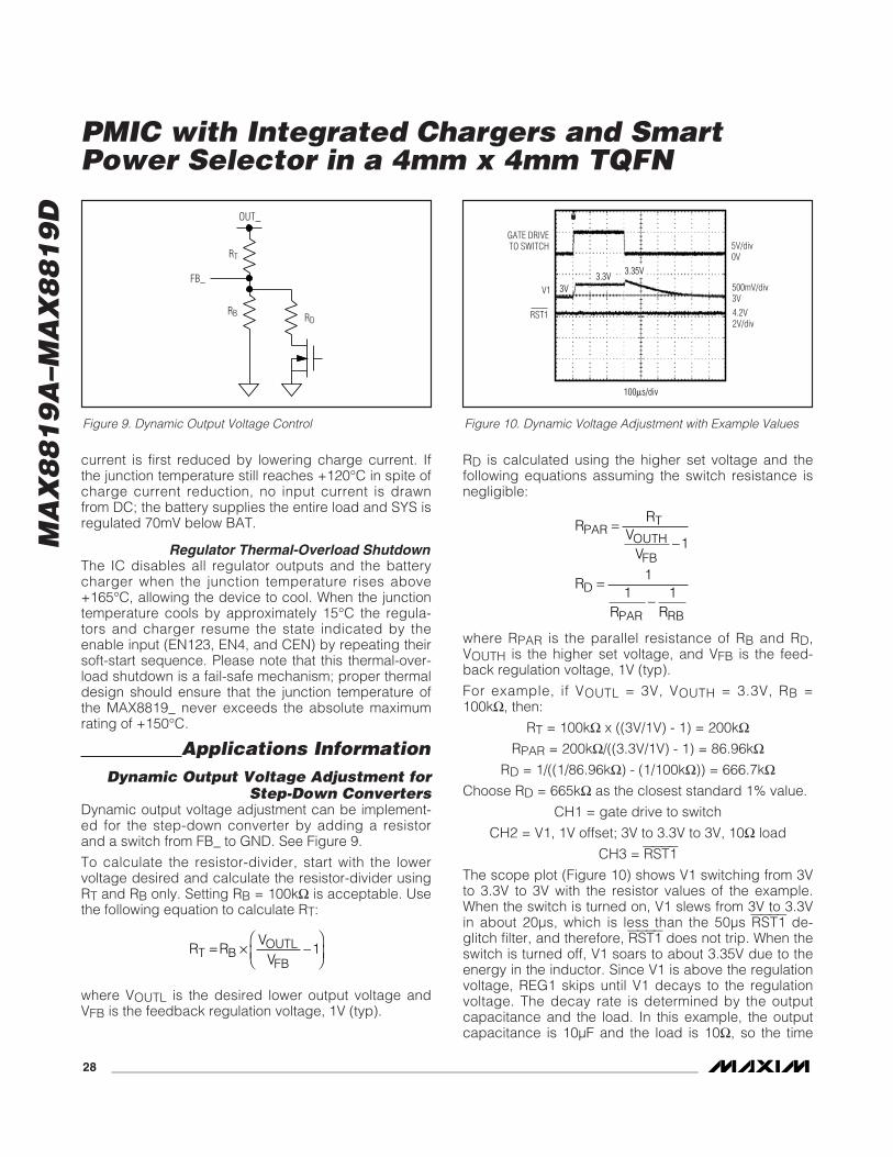
Applications InformationDynamic Output Voltage Adjustment for
Step-Down ConvertersDynamic output voltage adjustment can be implement-ed for the step-down converter by adding a resistorand a switch from FB_ to GND. See Figure 9.
To calculate the resistor-divider, start with the lowervoltage desired and calculate the resistor-divider usingRT and RB only. Setting RB = 100kΩ is acceptable. Usethe following equation to calculate RT:
where VOUTL is the desired lower output voltage andVFB is the feedback regulation voltage, 1V (typ).
RD is calculated using the higher set voltage and thefollowing equations assuming the switch resistance isnegligible:
where RPAR is the parallel resistance of RB and RD,VOUTH is the higher set voltage, and VFB is the feed-back regulation voltage, 1V (typ).
For example, if VOUTL = 3V, VOUTH = 3.3V, RB =100kΩ, then:
RT = 100kΩ x ((3V/1V) - 1) = 200kΩRPAR = 200kΩ/((3.3V/1V) - 1) = 86.96kΩ
RD = 1/((1/86.96kΩ) - (1/100kΩ)) = 666.7kΩChoose RD = 665kΩ as the closest standard 1% value.
CH1 = gate drive to switch
CH2 = V1, 1V offset; 3V to 3.3V to 3V, 10Ω load
CH3 = RST1
The scope plot (Figure 10) shows V1 switching from 3Vto 3.3V to 3V with the resistor values of the example.When the switch is turned on, V1 slews from 3V to 3.3Vin about 20μs, which is less than the 50μs RST1 de-glitch filter, and therefore, RST1 does not trip. When theswitch is turned off, V1 soars to about 3.35V due to theenergy in the inductor. Since V1 is above the regulationvoltage, REG1 skips until V1 decays to the regulationvoltage. The decay rate is determined by the outputcapacitance and the load. In this example, the outputcapacitance is 10μF and the load is 10Ω, so the time
RR
VV
R
R R
PART
OUTH
FB
D
PAR RB
=−
=−
1
11 1
R RV
VT BOUTL
FB= × −
⎛⎝⎜
⎞⎠⎟
1
OUT_
RT
RB RD
FB_
Figure 9. Dynamic Output Voltage Control
100μs/div
5V/div0V
500mV/div3V4.2V2V/div
3.35V3.3V3VV1
RST1
GATE DRIVETO SWITCH
Figure 10. Dynamic Voltage Adjustment with Example Values

MA
X8
81
9A
–MA
X8
81
9D
PMIC with Integrated Chargers and SmartPower Selector in a 4mm x 4mm TQFN
constant is R x C = 100μs, and the output voltagedecays to within 1% of final value in about 500μs.
PCB Layout and RoutingGood printed circuit board (PCB) layout is necessary toachieve optimal performance. Refer to the MAX8819AEvaluation Kit for Maxim’s recommended layout.
Use the following guidelines for the best results:
• The LX_ rapidly switches between PV_ and PG_.Minimize stray capacitance on LX_ to maintain highefficiency.
• Keep the FB_ node away from noise sources suchas the inductor.
• The exposed pad (EP) is the main path for heat toexit the IC. Connect EP to the ground plane withthermal vias to allow heat to dissipate from thedevice.
• Use short and wide traces for high-current and dis-continuous current paths.
• The step-down converter power inputs are criticaldiscontinuous current paths that require carefulbypassing. Place the step-down converter inputbypass capacitor as close as possible to the PV_and PG_ pins.
• Minimize the area of the loops formed by the step-down converters’ dynamic switching currents.
Package MarkingThe top of the MAX8819_ package is laser etched asshown in Figure 11:
“8819_ETI” is the product identification code. The fullpart number is MAX8819_ETI; however, in this case, the“MAX” prefix is omitted due to space limitations. The “_”corresponds to the “A” or “B” version.
“yww” is a date code. “y” is the last number in theGregorian calendar year. “ww” is the week number inthe Gregorian calendar. For example:
• “801” is the first week of 2008; the week ofJanuary 1st, 2008.
• “052” is the fifty-second week of 2010; the week ofDecember 27th, 2010.
• “aaaa” is an assembly code and lot code.
• “+” denotes lead-free packaging and marks thepin 1 location.
8819_ETI
TIyww
+ aaaa
Figure 11. Package Marking Example
MAX8819AMAX8819BMAX8819CMAX8819D
TOP VIEW
26
27
25
24
10
9
11FB
4
PG4
LX4
GND
EN4
12CO
MP4
PG3
PV13
LX1
DLIM
1
PG1
CHG
1 2
PV2
4 5 6 7
2021 19 17 16 15
LX2
PG2
CEN
DC
SYS
BATOV
P4LX
3
3
18
28 8DLIM2 RST1
EN123
23 13 FB1FB3
22 14 CISETFB2
+
EXPOSED PADDLE (EP)
Pin Configuration
Chip InformationPROCESS: S45T
PACKAGE TYPE PACKAGE CODE DOCUMENT NO.
28 TQFN-EP T2844+1 21-0139
Package InformationFor the latest package outline information and land patterns, goto www.maxim-ic.com/packages.
Maxim cannot assume responsibility for use of any circuitry other than circuitry entirely embodied in a Maxim product. No circuit patent licenses areimplied. Maxim reserves the right to change the circuitry and specifications without notice at any time.
Maxim Integrated Products, 120 San Gabriel Drive, Sunnyvale, CA 94086 408-737-7600 ____________________ 29
© 2008 Maxim Integrated Products is a registered trademark of Maxim Integrated Products, Inc.