ieee transactions on semiconductor manufacturing, … by synopsis. sentaurus device simulator is a...
TRANSCRIPT

IEEE TRANSACTIONS ON SEMICONDUCTOR MANUFACTURING, VOL. 29, NO. 2, MAY 2016 145
Process Variation Aware Design of Multi-ValuedSpintronic Memristor-Based Memory Arrays
Hassan Mostafa, Senior Member, IEEE, and Yehea Ismail, Fellow, IEEE
Abstract—The missing fourth passive element, predicted byL. Chua and denoted by memristor, has recently been in theresearch focus since its titanium dioxide thin film realization isreported by HP. Following that, the spintronic memristor, whichis based on the magnetic tunneling junction, is presented as analternative to the thin film memristor. The nano-scale geometrysize of the memristor makes it hard to control its dimensions dueto the process variation resulting from the fabrication process.This process variation results in yield degradation in the spin-tronic memristor-based memory arrays. This yield degradationis more significant when the spintronic memristor is utilized asa multi-valued memory elements. In this paper, the impact ofthe process variation on the spintronic memristor-based memoryyield is discussed for the 1-bit, 2-bit, and n-bit memory element.Moreover, two approaches are introduced to enhance the memoryyield.
Index Terms—Process variation, statistical yield, memristor,non-volatile memory.
I. INTRODUCTION
IN 1971, the father of the memristor, L. Chua, predictedthat there was a missing fourth passive circuit element and
denoted it by memristor [1]. The dream of having a real prac-tical realization of the memristor was on hold for 37 years. In2008, this dream has come true when R. S. Williams intro-duced a two-terminal Titanium dioxide (TiO2) nano-scale thinfilm device that follows the memristive characteristics definedby L. Chua in 1971 [2]. Recently, the memristor has gainedgreat attention on the device manufacturing, Computer-Aided-Design (CAD), circuit, and architecture levels [3]–[5]. Asstated by Kuekes et al. from HP, the memristor is the promis-ing candidate to replace the CMOS device in the near futurethanks to its smaller area [5]. There are two types of memristordevices: (1) thin-film memristor and (2) spintronic memris-tor. In this work, the main focus will be on the spintronicmemristor.
Manuscript received January 24, 2016; revised March 22, 2016; acceptedMarch 30, 2016. Date of publication April 6, 2016; date of current versionMay 3, 2016. This work was supported in part by the Zewail City of Scienceand Technology, in part by AUC, in part by the STDF, in part by Intel, in partby Mentor Graphics, in part by ITIDA, in part by SRC, in part by ASRT, inpart by NTRA, and in part by MCIT.
H. Mostafa is with the Electronics and Communications EngineeringDepartment, Cairo University, Giza 12613, Egypt, also with the Center forNanoelectronics and Devices, AUC, New Cairo, Egypt, New Cairo 11835,Egypt, and also with the Zewail City of Science and Technology, Giza 12588,Egypt. (e-mail: [email protected]).
Y. Ismail is with the Center for Nanoelectronics and Devices, AUC, andalso with the Zewail City of Science and Technology, Giza, Egypt.
Color versions of one or more of the figures in this paper are availableonline at http://ieeexplore.ieee.org.
Digital Object Identifier 10.1109/TSM.2016.2551224
Fig. 1. (a) Spintronic memristor structure and (b) Equivalent circuit model.
The need for high density memory structures has pushed thememory designers to give more attention to the next generationuniversal memories that is expected to replace the conven-tional memory technologies. The nonvolatile advantage of thespintronic memristor-based memory arrays promotes this tech-nology to be one of the most promising candidates for the nextgeneration memory technology.
Process variation affects on the spintronic memristor-basedmemories and results in write failure and/or read failure. Writefailure occurs when a logic ‘1’ is written into the memoryduring a write ‘0’ operation and vice versa. Similarly, whenthe memory provides a ‘1’ in a read ‘0’ operation, a readfailure occurs. Throughout this paper, the yield is defined asthe probability to write correctly to the memory and to readcorrectly from the memory. As process variation increases withthe device shrinking, the yield is degraded significantly.
The rest of the paper is organized as follows. In Section II,some background is given. The models used for the spin-tronic memristor and the statistical yield simulation setup arediscussed in Section III. Section IV presents the simulationsresults and discussions. Finally, some conclusions are drawnin Section V.
II. BACKGROUND
A. Spintronic Memristor
Figures 1.a and 1.b show the physical structure of thedomain wall spintronic memristor device and its equivalentcircuit model [3]. The device is composed of a thin oxidelayer sandwiched between two magnetic layers. One of thesetwo magnetic layers is pinned with a fixed magnetization andthe other one is a free layer with a domain wall as shownin Figure 1.a. The magnetization of the free layer on the
0894-6507 c© 2016 IEEE. Personal use is permitted, but republication/redistribution requires IEEE permission.See http://www.ieee.org/publications_standards/publications/rights/index.html for more information.
146 IEEE TRANSACTIONS ON SEMICONDUCTOR MANUFACTURING, VOL. 29, NO. 2, MAY 2016
left side of the domain wall is assumed to be aligned withthe magnetization of the pinned layer whereas, the right sidemagnetization is assumed to be in opposite direction to themagnetization of the pinned layer. Applying an external cur-rent, results in moving the domain wall depending on thecurrent direction [3].
Accordingly, the domain wall can be moved fully to theleft side resulting in a complete anti-parallel magnetizationbetween the free layer and the pinned layer which results ina high resistance denoted by Roff . On the other hand, if thedomain wall is fully moved towards the right side, a par-allel magnetization between the free layer and the pinnedlayers takes place and a low resistance denoted by Ron is real-ized between the two layers. The state variable w representsthe width of the parallel magnetization portion of the freelayer. The parallel region has low resistance while the anti-parallel region has higher resistance. The mathematical modelfor the spintronic memristor device memristance, M, is givenby [3], [4], [7]:
M(w) = Ron × w
D+ Roff ×
(1 − w
D
)(1)
where 0 ≤ w
D≤ 1.0
Applying an external current i results in changing the mem-ristance value as follows [3], [8], assuming the initial conditionis Ron:
M(q) = Ron + �vq
D× (
Roff − Ron)
(2)
where q =∫
jdt
where q is the applied external charge per unit area, j is thecurrent density, �v is the domain wall velocity coefficient, andD is the spintronic memristor thickness. It should be noted thatapplying a zero average external current has no net effect onthe spintronic memristance value as q = 0 in this case.
Moreover, in [3] and [4], the required charge to switch thememristance value from an arbitrary initial state M(w0) to adesired state M(w) is given by:
q =∣∣∣∣
D
�vRon(β − 1)× [M(w) − M(w0)]
∣∣∣∣
where β = Roff /Ron. (3)
B. Process Variation
Process variation affects the spintronic memristor deviceparameters, resulting in deviations in its electrical propertiesfrom the desired values [9]. The main sources of process vari-ation, that affect the spintronic memristor parameters, are theCritical Dimension Fluctuations (CDF) [8], [10], [11] and theLine Edge Roughness (LER) [3], [8], [11].
These variations can be captured mathematically as well asnumerically using Sentaurus device simulation tool providedby Synopsis. Sentaurus Device simulator is a general purposedevice simulation tool which offers simulation capability toexplore new device concepts for which fabrication processes
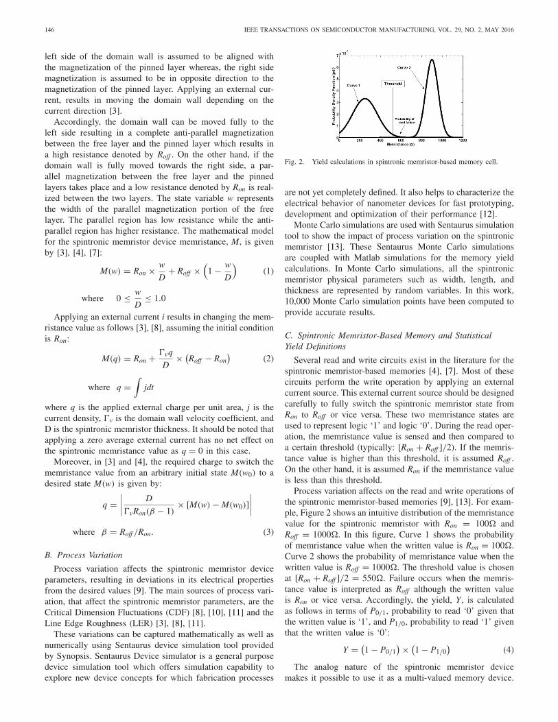
Fig. 2. Yield calculations in spintronic memristor-based memory cell.
are not yet completely defined. It also helps to characterize theelectrical behavior of nanometer devices for fast prototyping,development and optimization of their performance [12].
Monte Carlo simulations are used with Sentaurus simulationtool to show the impact of process variation on the spintronicmemristor [13]. These Sentaurus Monte Carlo simulationsare coupled with Matlab simulations for the memory yieldcalculations. In Monte Carlo simulations, all the spintronicmemristor physical parameters such as width, length, andthickness are represented by random variables. In this work,10,000 Monte Carlo simulation points have been computed toprovide accurate results.
C. Spintronic Memristor-Based Memory and StatisticalYield Definitions
Several read and write circuits exist in the literature for thespintronic memristor-based memories [4], [7]. Most of thesecircuits perform the write operation by applying an externalcurrent source. This external current source should be designedcarefully to fully switch the spintronic memristor state fromRon to Roff or vice versa. These two memristance states areused to represent logic ‘1’ and logic ‘0’. During the read oper-ation, the memristance value is sensed and then compared toa certain threshold (typically: [Ron + Roff ]/2). If the memris-tance value is higher than this threshold, it is assumed Roff .On the other hand, it is assumed Ron if the memristance valueis less than this threshold.
Process variation affects on the read and write operations ofthe spintronic memristor-based memories [9], [13]. For exam-ple, Figure 2 shows an intuitive distribution of the memristancevalue for the spintronic memristor with Ron = 100� andRoff = 1000�. In this figure, Curve 1 shows the probabilityof memristance value when the written value is Ron = 100�.Curve 2 shows the probability of memristance value when thewritten value is Roff = 1000�. The threshold value is chosenat [Ron + Roff ]/2 = 550�. Failure occurs when the memris-tance value is interpreted as Roff although the written valueis Ron or vice versa. Accordingly, the yield, Y , is calculatedas follows in terms of P0/1, probability to read ‘0’ given thatthe written value is ‘1’, and P1/0, probability to read ‘1’ giventhat the written value is ‘0’:
Y = (1 − P0/1
) × (1 − P1/0
)(4)
The analog nature of the spintronic memristor devicemakes it possible to use it as a multi-valued memory device.

MOSTAFA AND ISMAIL: PROCESS VARIATION AWARE DESIGN 147
Fig. 3. Yield calculations in 2-bit spintronic memristor-based memories.
This means that instead of using the spintronic memristordevice to store only 1-bit (i.e., two states either Ron or Roff ), itcan be used to store multiple states such as “00”, “01”, “10”,and “11”. In the 2-bit memristor case, there will be three dif-ferent thresholds instead of the one threshold used for the 1-bitcase. In general, the spintronic memristor device can be usedfor n-valued memory storage where n is a nonzero integer.However, considering the process variations, there are severallimitations that are imposed on the multi-valued memristor-based memory design that will place an upper limit for n. Ingeneral, the higher the value of n, the lower the achieved mem-ory yield. Figure 3 illustrates how the yield is degraded whenthe spintronic memristor is used as a 2-bit memory device.Curves 1, 2, 3, and 4 represent the probability density func-tion of the memristance value when states “00”, “01”, “10”,and “11” are written, respectively.
III. SIMULATION SETUP
A. Variation Models and Yield Calculations
In [3] and [8], a statistical model of the spintronic memris-tor has been introduced and verified by using 3D Monte Carlodevice simulations. Unfortunately, this model works only for aspecific size of the spintronic memristor (typically: a spintronicmemristor structure with dimensions 200nm × 10nm × 7nm).In this work, the analytical model in [8] is integrated withthe Synopsis Sentaurus device simulator tool. In these MonteCarlo simulations, all the spintronic memristor physical param-eters such as length, width, and thickness are representedby random variables and 10,000 Monte Carlo simulationpoints have been computed to provide accurate variationresults [3], [8]. The analytical model in [8] defined several fit-ting parameters which are extracted from the 3D Monte Carlosimulations carried out by using the Synopsis Sentaurus devicesimulator tool for the 200nm×10nm×7nm spintronic memris-tor device. In this work, these fitting parameters are extractedwhen the memristor dimensions are varied.
Following the extraction of the analytical models fittingparameters, the probability distribution function of the mem-ristance is plotted. The memory yield is calculated for thespintronic memristor-based memory array. It should be notedthat each yield point is calculated by using the analytical model(Matlab simulations with the extracted parameters) and veri-fied by using the 10,000 points 3D Monte Carlo Simulations.The yield calculations are repeated for different spintronicmemristor sizes to show the impact of the process variation on
the spintronic memristor-based memory when the spintronicmemristor size is varied.
It should be noted that all the memristor parameters areassumed to be normally distributed because according to [14],the usage of the central limit theorem helps to model thesum of a sufficiently large number of non-normally distributedrandom variables as a normal distribution [15]. In [16], thesum of 16 random variables is a sufficient number to validatethis theory. For example, the leakage current of the flip-flopor the SRAM cell exhibits a log-normal distribution, however,the distribution of the total leakage current of 16 flip-flopsor 16 SRAM cells follows a normal distribution as verifiedin [16] and [17], respectively.
B. Statistical Yield Optimization
After showing the impact of the process variation on thespintronic memristor-based memory yield, two approaches areused to optimize the yield as follows:
1) Optimal Write Current: In the write operation, a spe-cific external current should be applied to switch the spin-tronic memristor from the Ron state to the Roff state or viceversa [4], [7]. However, the existence of the process variationmight prevent this applied external current from achieving thistask [18]. For example, assume the required current to switchthe spintronic memristor from Ron to Roff is 10μA for a dura-tion of 5nsec. This current might not be sufficient to increasethe memristance value above the threshold value (typically:[Ron + Roff ]/2) due to process variation. Accordingly, a writefailure occurs because in an attempt to write ‘1’ (assumingRoff represents logic ‘1’), the resulting memristance value isstill less than the threshold and will be read as ‘0’ (assumingRon represents logic ‘0’). Correspondingly, this write charge(q = 10μA × 5nsec) should be increased to ensure that thememristance value at least exceeds this threshold. In this work,the optimization problem is to find the optimal charge thatmaximizes the yield.
Therefore, the yield is calculated for different charge val-ues and the optimal charge that results in the maximum yieldis obtained for the spintronic memristor. This optimizationproblem has been solved by using Matlab simulations andcurve fitting is used to find the relationship between the opti-mal charge and the nominal charge (i.e., the charge usedwhen the process variation is not taken into account givenby (3) [3], [4]) for different memristor sizes. Afterwards, thesame work is repeated for the 2-bit spintronic memristor andthe n-bit spintronic memristor.
2) Optimal Threshold: In the read operation, the devicememristance value is sensed and compared to the thresholdvalue [Ron +Roff ]/2. For example, in a read ‘0’ operation, thesensed memristance value should be less than this threshold.Due to process variations, the sensed memristance value mightbe larger than this threshold and interpreted as logic ‘1’ andaccordingly a read failure occurs. In this work, an optimizationproblem has been solved to find the optimal threshold value(other than the mid-way threshold) that results in maximumyield. It should be noted that the net external charge should

148 IEEE TRANSACTIONS ON SEMICONDUCTOR MANUFACTURING, VOL. 29, NO. 2, MAY 2016
be zero in the read operation in order not to destroy the storedvalue.
Thus, the yield is calculated for different threshold val-ues and the optimal threshold that results in the maximumyield is obtained for the spintronic memristor-based memory.This optimization problem has been solved by using Matlabsimulations and curve fitting is used to find the relation-ship between the optimal threshold and the nominal threshold(i.e., the threshold used when the process variation is not con-sidered) for different memristor sizes. Afterwards, the samework is repeated for the 2-bit spintronic memristor and then-bit spintronic memristor.
The following steps summarize the overall yield improve-ment design flow:
1) The memristor dimensions and material type as well asthe process variation model are applied to the devicesimulator. In this work case study, the spintronic memris-tor and the process variation models given in [3] and [8]are used.
2) The outcome of the device simulator is the memristanceparameters variations such as Ron, Roff , and w/D. Thisoutcome is fitted with the process variation model to findthe fitting parameters for each memristor size. 10,000 3DMonte Carlo points are used to provide high accuracy.
3) The memristance parameters variations are applied toMatlab as well as the memristor model and the requiredmulti-level value n (i.e., n = 1 for single bit memristormemory cell and n = 2 for 2-bit memristor memorycell). In this work case study, the model in [3] and [8]is used as other more accurate models are only definedfor one memristor size such as TEAM model [19]. Theoutcome of the Matlab is the yield value.
4) Following the yield calculations, the Matlab is used tofind the optimal write currents and optimal thresholdsthat result in maximum yield. The maximum yield isalso calculated.
5) The maximum yield achieved (with optimal write cur-rents and optimal thresholds) is compared with a givenyield (i.e., 99.9% in this work case study) and the mini-mum memristor dimension required to achieve this yieldis calculated for different n values.
IV. SIMULATION RESULTS AND DISCUSSION
It should be stated clearly that the main objective of thispaper is to introduce a statistical yield improvement flowregardless of the used memristor models or process variationmodels. In other words, the accuracy of the statistical yieldsimulation flow is limited by the used models accuracy andthere is a trade-off between the accuracy of the proposed sta-tistical yield flow and the computational time (i.e., to havemore accurate simulation results, a longer computation time isneeded). The memristor model used is the model in [3] and [8]because it works for different memristor sizes by feeding thevariations distribution of the memristor parameters Ron, Roff ,and w/D obtained from the Sentaurus device simulator CADtool for different memristor sizes to the model to calculate thememristance probability distribution function. Although this
Fig. 4. Yield with no optimization for different sizes of the 1-bit memristor.
model in [3] and [8] is not very accurate, other models inthe literature such as TEAM model [19] are limited to onlyone memristor size and accordingly, can not be used in theproposed flow case study.
A. 1-Bit Memristor-Based Memory
1) Optimal Write Current: Figure 4 shows the yield val-ues for different spintronic memristor device where W is thedevice width, L is the device length, and D is the devicethickness. In this case the nominal charge defined in (3) isused which is sufficient to switch the memristance from Ron
to Roff and vice versa when the process variation is ignoredand nominal threshold value is used (i.e., [Ron + Roff ]/2).It is clear that the yield is improved for larger device size.For example, a spintronic memristor device with dimensionsW = 100nm, L = 10nm, and D = 3nm exhibits a yield of51.9% whereas a spintronic memristor device with dimensionsW = 1000nm, L = 100nm, and D = 100nm exhibits a yieldof 99.9%.
The optimization setup discussed above is applied to findthe optimal charge that maximizes the yield. Figure 5 dis-plays the yield improvement achieved when the optimizationmethod is adopted for different memristor sizes. It is inter-esting to observe that depending on the memristor size, theproposed optimization method achieves higher yield values.For example, for a spintronic memristor with dimensionsW = 100nm, L = 10nm, and D = 3nm, the yield improvedfrom 51.9% to 77.9% whereas the yield is improved from 77%to 94.5% when the memristor dimensions are W = 100nm,
L = 10nm, and D = 100nm.The optimal charge values required to achieve the maximum
yield is plotted versus the nominal charge values for differentmemristor device sizes in Figure 6 at the nominal thresholdvalues. Each point in this figure represents a specific spintronicmemristor device dimensions. It is obvious that the optimalcharge is always larger than the nominal charge and its typ-ical value is qoptimal ≈ 1.45 × qnominal by using curve fittingon Figure 6. Therefore, to maximize the yield, the nominalcharge defined in (3) should be increased by 45%. It shouldbe noted that the increase in the nominal charge by 45% resultsin shifting the probability density function of Ron (i.e., Curve 1in Figure 2) to the left and the probability density function ofRoff (i.e., Curve 2 in Figure 2) to the right. Accordingly, thisnominal charge increase enhances the memory yield.
2) Optimal Threshold: Figure 4 displays the yield whenthe threshold is fixed at the nominal value of [Ron + Roff ]/2

MOSTAFA AND ISMAIL: PROCESS VARIATION AWARE DESIGN 149
Fig. 5. Nominal and optimal yield (optimal write current) at the nominalthreshold for the 1-bit memristor when (a) D = 3nm and (b) D = 100nm.
Fig. 6. Optimal charge versus the nominal charge.
for different memristor device sizes at the nominal write cur-rent values. The optimization setup discussed above is appliedto find the optimal threshold value other than [Ron + Roff ]/2that maximizes the yield. Figure 7 displays the yield improve-ment achieved when the optimization method is adopted fordifferent memristor sizes. The proposed optimization methodimproves the yield values.
The optimal threshold values required to achieve the max-imum yield is plotted versus the nominal threshold values(i.e., [Ron + Roff ]/2) for different spintronic memristor devicesizes in Figure 8 at nominal write current values given in (3).Each point in this figure represents a specific memristor devicedimensions. It is obvious that the optimal threshold is alwayslarger than the nominal threshold and its typical value isThresholdoptimal ≈ 1.15 × Thresholdnominal by using curve fit-ting on Figure 8. Therefore, to maximize the yield, the nominalthreshold defined in [3] and [8] (i.e., [Ron + Roff ]/2) shouldbe increased by 15%. It should be noted that the increase inthe nominal threshold by 15% results in shifting the thresholdvalue (i.e., the threshold value at 500 � in Figure 2) to theright which improves the memory yield.
Fig. 7. Nominal and optimal yield (optimal threshold) at the nominal writecurrent for the 1-bit memristor when (a) D = 3nm and (b) D = 100nm.
Fig. 8. Optimal threshold versus nominal threshold.
3) Optimal Write Current and Optimal Threshold: Usingthe guidelines obtained above for the optimal write current(i.e., qoptimal ≈ 1.45 × qnominal) and the optimal threshold(i.e., Thresholdoptimal ≈ 1.15 × Thresholdnominal), Figure 9displays the yield when the optimal charge and the opti-mal threshold are adopted for different spintronic memristordevice sizes. It should be highlighted that the minimum spin-tronic memristor device size to achieve a yield of 99.9% whenthe optimal charge and the optimal threshold are utilized isW = 900nm, L = 90nm, and D = 100nm. This size is smallerthan the minimum spintronic memristor device size to achievethe same yield when no optimization is utilized (this mini-mum size is calculated to be W = 500nm, L = 50nm, andD = 70nm) by a factor of 4.6X. Correspondingly, the pro-posed optimization method results in increasing the memorydensity by a factor of 4.6X to achieve the same yield of 99.9%.
B. 2-Bit Spintronic Memristor-Based MemoryYield Optimization
The 2-bit spintronic memristor-based memory is designedby dividing the memristance range (i.e., Roff − Ron) into four

150 IEEE TRANSACTIONS ON SEMICONDUCTOR MANUFACTURING, VOL. 29, NO. 2, MAY 2016
Fig. 9. Nominal and optimal yield (optimal write current and optimalthreshold) for the 1-bit memristor when (a) D = 3nm and (b) D = 100nm.
Fig. 10. Mean values and bounds for the 2-bit memristor-based memory cell.
equal regions where each region is assigned a 2-bits value(i.e., “00”, “01”, “10”, or “11”) as displayed in Figure 10.Figure 10 illustrates also the threshold values for these regions(i.e., T1, T2, and T3) and their mean values (i.e., M1, M2,M3, and M4). In this figure, T2 = [Ron + Roff ]/2, T1 =[Ron +T2]/2, T3 = [T2+Roff ]/2, M1 = [Ron +T1]/2, M2 =[T1 + T2]/2, M3 = [T2 + T3]/2, and M4 = [T3 + Roff ]/2.
Therefore, in order to write “00”, the input charge shouldchange the memristance value from the initial value to M1.Therefore, the input charge depends on the initial state whichis assumed to be the worst case (maximum charge) through-out this work (i.e., the initial state is assumed “11” when weneed to write “00” and the required charge should change thememristance state from M4 to M1). Also, for the read oper-ation, the memristance value is sensed and compared to thethresholds (i.e., Ron, T1, T2, T3, and Roff ).
1) Optimal Write Currents: Figure 11 shows the yield val-ues for different spintronic memristor devices where W is thedevice width, L is the device length, and D is the devicethickness. In this case, the nominal charge defined in (3)is used which is sufficient to switch the memristance fromthe initial worst case mean value to the desired mean valuewhen the process variation is ignored. For example, to cal-culate the yield for the “00” case, the required charge tochange the memristance state from M4 to M1 is calculated byusing (3). Following that, 10,000 point Monte Carlo analysis
Fig. 11. Yield with no optimization for the 2-bit memristor.
is conducted to calculate the yield. The yield is first calcu-lated for each case (i.e., “00”, “01”, “10”, and “11”) andthen the overall yield is calculated. According to Figure 11,it is clear that the yield is improved for larger devicesizes.
The optimization setup discussed above is applied to findthe optimal charges that maximize the overall yield denotedby qwrite“00”, qwrite“01”, qwrite“10”, and qwrite“11”.
The optimal charges values required to achieve the maxi-mum yield are determined for different memristor device sizesand the curve fitting method is performed to conclude that thecharges qwrite“00”, qwrite“01”, qwrite“10”, and qwrite“11” should beincreased by 45%, 22%, 36%, and 45%, respectively. It shouldbe noted that the optimal charges qwrite“00” and qwrite“11” areincreased by the same amount similar to the 1-bit memristormemory cell case because the worst case charges to write “00”or “11” are the charges required to switch Ron to Roff and viceversa.
2) Optimal Thresholds: Figure 11 displays the yield whenthe thresholds are fixed at their nominal values of T1 =[Ron + T2]/2, T2 = [Ron + Roff ]/2, and T3 = [T2 + Roff ]/2for different spintronic memristor device sizes and the nomi-nal write currents. The optimization setup discussed above isapplied to find the optimal thresholds values that maximizethe yield.
The optimal thresholds values required to achieve the max-imum yield are determined for different spintronic memristordevice sizes and the curve fitting method is performed to con-clude that the thresholds T1, T2, and T3 should be increasedby 8%, 15%, and 12%, respectively.
3) Optimal Write Currents and Optimal Thresholds:Using the guidelines obtained above for the optimal writecurrents and the optimal thresholds, Figure 12 displays theyield when the optimal charges and the optimal thresholdsare adopted for different spintronic memristor device sizes. Itshould be highlighted that the minimum memristor device sizeto achieve a yield of 99.9% when the optimal charges and theoptimal thresholds are utilized is W = 1000nm, L = 100nm,
and D = 120nm. This size is smaller than the minimummemristor device size to achieve the same yield when nooptimization is utilized (this minimum size is calculated to be2000nm×200nm×150nm) by a factor of 5X. Correspondingly,the proposed optimization method results in increasing thememory density by a factor of 5X to achieve the same yieldof 99.9%.

MOSTAFA AND ISMAIL: PROCESS VARIATION AWARE DESIGN 151
Fig. 12. Nominal and optimal yield (optimal write currents and optimalthresholds) for the 2-bit memristor when (a) D = 3nm and (b) D = 100nm.
TABLE IMINIMUM MEMRISTOR DEVICE SIZE (W × L × D) TO ACHIEVE AN
OVERALL YIELD OF 99.9% FOR THE NOMINAL CASE AND THE
OPTIMIZED CASE FOR DIFFERENT VALUES OF n
C. n-Bit Spintronic Memristor-Based MemoryYield Optimization
The n-bit memristor-based memory is designed by dividingthe memristance range (i.e., Roff − Ron) into 2n equal regionswhere each region is assigned an n-bits value (i.e., “000”,“001”, “010”, “011”, “100”, “101”, “110”, or “111” whenn = 3). In the n-bit case, there are 2n mean values and 2n − 1threshold values. In the following the overall yield is calculatedbased on the same setup used before.
The same simulations carried out for the 1-bit and 2-bit spin-tronic memristor-based memory cases are conducted again forthe n-bit case when n changes from 1 to 5. Using the optimalwrite currents and the optimal thresholds, Figure 13 displaysthe yield when the optimal charges and the optimal thresholdsare adopted for different spintronic memristor device sizes. Itshould be highlighted that the minimum memristor device sizeto achieve a yield of 99.9% when the optimal charges and theoptimal thresholds are utilized is dependent on the multi-bitvalue n.
Fig. 13. Nominal and optimal yield (optimal write currents and optimalthresholds) for the n-bit memristor with size (a) W = 100nm, L = 10nm, andD = 3nm and (b) W = 1000nm, L = 100nm, and D = 100nm.
Table I lists the minimum spintronic memristor devicedimensions required to achieve a yield of 99.9% for differ-ent values of n when the optimization method is not adoptedand when it is adopted. It is clear from this table that theadoption of the optimization method results in reducing theminimum n-bit memristor device size required to achieve ayield of 99.9% by a factor ranging from 4.6X to 10X.
V. CONCLUSION
In this paper, a statistical yield model for the spintronicmemristor has been developed and verified by using theSentaurus device simulator 3D Monte Carlo analysis. Theimpact of the process variation on the spintronic memristor-based memory has been investigated for the 1-bit, 2-bit, andn-bit memory arrays. Simulation results show that the pro-cess variation imposes limitations on the utilization of themulti-value memristor-based memory and there is a mini-mum spintronic memristor size that should be used to achievea memory yield of 99.9%. In addition, two approaches areproposed to improve the memory yield which are the opti-mal write current and the optimal threshold. For example,for the 1-bit memristor-based memory arrays, the nominalwrite current should be increased by 45% and the nominalthreshold value should be increased by 15% to achieve themaximum yield. This work can be extended for other mem-ristor types such as thin-film memristor and the three-terminalsmemristor.
REFERENCES
[1] L. Chua, “Memristor—The missing circuit element,” IEEE Trans. CircuitTheory, vol. 18, no. 5, pp. 507–519, Sep. 1971.

152 IEEE TRANSACTIONS ON SEMICONDUCTOR MANUFACTURING, VOL. 29, NO. 2, MAY 2016
[2] D. B. Strukov, G. S. Snider, D. R. Stewart, and R. S. Williams, “Themissing memristor found,” Nature, vol. 453, pp. 80–83, May 2008.
[3] Y. Chen and X. Wang, “Compact modeling and corner analysis ofspintronic memristor,” in Proc. IEEE/ACM Int. Symp. NANOARCH,San Francisco, CA, USA, Jul. 2009, pp. 7–12.
[4] Y. Ho, G. M. Huang, and P. Li, “Dynamical properties anddesign analysis for nonvolatile memristor memories,” IEEE Trans.Circuits Syst. I, Reg. Papers, vol. 58, no. 4, pp. 724–736,Apr. 2011.
[5] P. J. Kuekes, D. R. Stewart, and R. S. Williams, “The crossbar latch:Logic value storage, restoration, and inversion in crossbar circuits,”J. Appl. Phys., vol. 97, no. 3, 2005, Art. no. 034301.
[6] A. Dayal, P. Li, and G. M. Huang, “Robust SRAM designvia joint sizing and voltage optimization under dynamic stabil-ity constraints,” J. Low Power Electron., vol. 6, no. 1, pp. 66–79,2010.
[7] M. Elshamy, H. Mostafa, Y. H. Ghallab, and M. S. Said, “A novelnondestructive read/write circuit for memristor-based memory arrays,”IEEE Trans. Very Large Scale Integr. (VLSI) Syst., vol. 23, no. 11,pp. 2648–2656, Nov. 2015.
[8] M. Hu, H. Li, Y. Chen, X. Wang, and R. E. Pino, “Geometry variationsanalysis of TiO2 thin-film and spintronic memristors,” in Proc. 16thIEEE Asia South Pac. Design Autom. Conf. (ASP-DAC), Yokohama,Japan, 2011, pp. 25–30.
[9] R. Naous, M. Al-Shedivat, and K. N. Salama, “Stochasticity modelingin memristors,” IEEE Trans. Nanotechnol., vol. 15, no. 1, pp. 15–28,Jan. 2016.
[10] H. Mostafa, M. Anis, and M. Elmasry, “A design-oriented softerror rate variation model accounting for both die-to-die and within-die variations in submicrometer CMOS SRAM cells,” IEEE Trans.Circuits Syst. I, Reg. Papers, vol. 57, no. 6, pp. 1298–1311,Jun. 2010.
[11] H. Mostafa and Y. Ismail, “Statistical yield improvement underprocess variations of multi-valued memristor-based memories,”Microelectron. J., vol. 51, pp. 46–57, May 2016.
[12] Synopsis Articles. (Feb. 2016). An Advanced Multidimensional(1D/2D/3D) Device Simulator. [Online]. Available: http://www.synopsys.com/Tools/TCAD/DeviceSimulation/Pages/SentaurusDevice.aspx
[13] B. Liu et al., “Vortex: Variation-aware training for memristor X-bar,”in Proc. 52nd IEEE/ACM/EDAC DAC, San Francisco, CA, USA, 2015,pp. 1–6.
[14] A. Papoulis, Probability, Random Variables, and Stochastic Processes,3rd ed. New York, NY, USA: McGraw-Hill, 1991.
[15] S. Mukhopadhyay, H. Mahmoodi, and K. Roy, “Modeling of fail-ure probability and statistical design of SRAM array for yieldenhancement in nanoscaled CMOS,” IEEE Trans. Comput.-AidedDesign Integr. Circuits Syst., vol. 24, no. 12, pp. 1859–1880,Dec. 2005.
[16] V. Gupta and M. Anis, “Statistical design of the 6T SRAM bit cell,”IEEE Trans. Circuits Syst. I, Reg. Papers, vol. 57, no. 1, pp. 93–104,Jan. 2010.
[17] S. A. Sadrossadat, H. Mostafa, and M. Anis, “Statistical designframework of submicron flip-flop circuits considering process vari-ations,” IEEE Trans. Semicond. Manuf., vol. 24, no. 1, pp. 69–79,Feb. 2011.
[18] J. Rajendran, R. Karri, and G. S. Rose, “Improving toleranceto variations in memristor-based applications using parallel mem-ristors,” IEEE Trans. Comput., vol. 64, no. 3, pp. 733–746,Mar. 2015.
[19] S. Kvatinsky, E. G. Friedman, A. Kolodny, and U. C. Weiser, “TEAM:Threshold adaptive memristor model,” IEEE Trans. Circuits Syst. I, Reg.Papers, vol. 60, no. 1, pp. 211–221, Jan. 2013.
Hassan Mostafa (S’01–M’11–SM’15) received theB.Sc. and M.A.Sc. degrees (Hons.) in electronicsengineering from Cairo University, Cairo, Egypt, in2001 and 2005, respectively, and the Ph.D. degreein electrical and computer engineering from theDepartment of Electrical and Computer Engineering,University of Waterloo, Waterloo, ON, Canada, in2011.
He is currently an Assistant Professor with theElectronics and Communications Department, CairoUniversity, and also an Adjunct Assistant Professor
with the Center for Nano-Electronics and Devices, American University inCairo, Cairo. He has worked as an Natural Sciences and Engineering ResearchCouncil of Canada (NSERC) Post-Doctoral Fellow with the Department ofElectrical and Computer Engineering, University of Toronto, Toronto, ON,Canada. His Post-Doctoral Research includes the design of the next genera-tion FPGA in collaboration with Fujitsu Research Laboratory, Japan/USA.
He is collaborating with several sponsors across the world such asIntel, USA, Fujitsu, Japan, National Telecommunications Regulation Agency,Egypt, the University of Toronto, the University of Waterloo, the Academyof Scientific Research and Technology, Egypt, NSERC, Cairo University,Blackberry, Canada, Qatar National Research Fund, Qatar.
He has authored/coauthored over 80 papers in international journals andconferences and published four books. His research interests include analog-to-digital converters, low-power circuits, subthreshold logic, variation-tolerantdesign, soft error tolerant design, statistical design methodologies, next gener-ation FPGA, spintronics, memristors, energy harvesting MEMS/NEMS, powermanagement, and optoelectronics.
Dr. Mostafa was a recipient of the University of Toronto Research AssociateScholarship in 2012, the NESRC Prestigious Post-Doctoral Fellowship in2011, the Waterloo Institute of Nano-Technology Nanofellowship ResearchExcellence Award in 2010, the Ontario Graduate Scholarship in 2009, andthe University of Waterloo SandFord Fleming TA Excellence Award in 2008.
Yehea Ismail (F’13) is the Director of theNanoelectronics and Devices Center, Zewail City,and the American University in Cairo.
He is an Editor-in-Chief of the IEEETRANSACTIONS ON VERY LARGE SCALE
INTEGRATION (VLSI) SYSTEMS and the ChairElect of the IEEE VLSI technical committee. Heis on the Editorial Board of the Journal of Circuits,Systems, and Computers, was on the EditorialBoard of the IEEE TRANSACTIONS ON CIRCUITS
AND SYSTEMS I: FUNDAMENTAL THEORY AND
APPLICATIONS, and the Guest Editor for a special issue of the IEEETRANSACTIONS ON VERY LARGE SCALE INTEGRATION (VLSI) SYSTEMS
on SOn-Chip Inductance in High Speed Integrated Circuits.T He has alsochaired many conferences such as GLSVLSI, IWSOC, and ISCAS. He isthe Chief Scientist of the Innovation and Entrepreneurship Center of theMinistry of Communications and Information Technology, Egypt.
Prof. Ismail was a recipient of several awards such as the USA NationalScience Foundation Career Award, the IEEE CAS Outstanding AuthorAward, the Best Teacher Award at Northwestern University, and many otherbest teaching awards and best paper awards. He is the Distinguished Lecturerof the IEEE CASS.
He has published over 170 papers in top refereed journals and conferencesand many patents. He has co-authored three books entitles On-ChipInductance in High Speed Integrated Circuits, Handbook on Algorithms forVLSI Physical Design, and Temperature-Aware Computer Architecture. Hehas many patents in the area of high performance circuits and interconnectdesign and modeling. His work is some of the most highly cited in the verylarge scale integration area and is extensively used by industry.