98 ieee transactions on electron devices, … · accurate capacitance modeling and characterization...
TRANSCRIPT

98 IEEE TRANSACTIONS ON ELECTRON DEVICES, VOL. 61, NO. 1, JANUARY 2014
Accurate Capacitance Modeling andCharacterization of Organic Thin-Film Transistors
Tarek Zaki, Student Member, IEEE, Susanne Scheinert, Ingo Hörselmann, Reinhold Rödel,Florian Letzkus, Harald Richter, Ute Zschieschang, Hagen Klauk, Member, IEEE,
and Joachim N. Burghartz, Fellow, IEEE
Abstract— This paper presents analysis of the charge storagebehavior in organic thin-film transistors (OTFTs) by means ofadmittance characterization, compact modeling, and 2-D devicesimulation. The measurements are performed for frequenciesranging from 100 Hz to 1 MHz and bias potentials from zeroto −3 V on top-contact OTFTs that employ air-stable and high-mobility dinaphtho-thieno-thiophene as the organic semiconduc-tor. It is demonstrated that the dependence of the intrinsic OTFTgate–source and gate–drain capacitances on the applied voltagesagrees very well with Meyer’s capacitance model. Furthermore,the impact of parasitic elements, including fringe current andcontact impedance, is investigated. The parameters used forthe simulation and modeling of all the dynamic characteristicscorrespond closely to those extracted from static measurements.Finally, the implications of the admittance measurements arealso discussed relating to the OTFTs dynamic performance,particularly the cutoff frequency and the charge response time.
Index Terms— Admittance measurement, channel capacitance,device modeling and simulation, organic thin-film transistors.
I. INTRODUCTION
ORGANIC thin-film transistors (OTFTs) are now makingsignificant inroads into many new large-area applica-
tions, considering that they can be fabricated at low tem-peratures and with high throughput on a wide range ofunconventional substrates, such as glass, plastic, fabric, andpaper [1]. For further development, it is essential to under-stand the device physics and to study the limits of thedevice performance to be able to accurately model theirbehavior. The steady-state characteristics of the OTFTs havebeen extensively studied [2]–[4]. Vissenberg and Matters [2]have proposed an analytical model to describe the gate-voltage dependence of the field-effect mobility of OTFTs—an effect that was originally perceived by Brown et al. [3].
Manuscript received August 21, 2013; revised November 12, 2013; acceptedNovember 18, 2013. Date of publication December 5, 2013; date of currentversion December 20, 2013. This work was supported by the German ResearchFoundation under Grant BU 1962/4-1. The review of this paper was arrangedby Editor D. J. Gundlach.
T. Zaki and J. N. Burghartz are with the University of Stuttgart, Stuttgart70569, Germany, and also with the Institute for Microelectronics Stuttgart,Stuttgart 70569, Germany (e-mail: [email protected]).
S. Scheinert and I. Hörselmann are with the Ilmenau University of Tech-nology, Ilmenau 98684, Germany.
R. Rödel, U. Zschieschang, and H. Klauk are with the Max Planck Institutefor Solid State Research, Stuttgart 70569, Germany.
F. Letzkus and H. Richter are with the Institute for MicroelectronicsStuttgart, Stuttgart 70569, Germany.
Color versions of one or more of the figures in this paper are availableonline at http://ieeexplore.ieee.org.
Digital Object Identifier 10.1109/TED.2013.2292390
Fig. 1. Schematic cross section of the fabricated inverted-staggered (bottom-gate, top-contact) OTFT, where L is the channel length and Lov is thegate-to-contact overlap. The molecular structure of the used dinaphtho-thieno-thiophene OSC is designated.
Based on that common point, Marinov and Deen [4] havederived an OTFT compact DC model that is valid for alloperating regimes, i.e., linear and saturation above thresh-old, subthreshold, and reverse biasing. As for the dynamiccharacteristics of the OTFTs, recent works have reportedS-parameter measurements of OTFTs to characterize the cutofffrequency [5], and also to study the influence of uninten-tional process misalignment between the device terminalson the dynamic performance [6]. Further investigations haveused admittance measurements to model the OTFT channeland to describe the current injection mechanism throughthe contact interfaces between the metallic source/drainand the organic semiconductor (OSC) layers [7]–[11].It has been proposed in [11] to adopt Meyer’s model [12],which is used for silicon-based MOSFETs, to describe thecharge storage effects of the OTFTs intrinsic capacitances.However, what is lacking at this point is a verification ofthis proposal by adequate comparison between capacitancemeasurements and simulations.
In this paper, we present experimental analysis of theOTFTs intrinsic capacitances at different biasing potentialsand validate the results with accurate modeling as well as2-D device simulations. Effects induced by the parasiticelements that extend beyond the periphery of the intrinsictransistor are carefully considered. We also investigate thefrequency response of OTFTs by means of admittance mea-surements. A small-signal model is built to characterize boththe resistive and the reactive parts of the measured deviceadmittance.
II. OTFT FABRICATION
As shown in Fig. 1, the inverted-staggered OTFT structure,which is also referred to as top-contact/bottom-gate configura-tion, was used for our OTFTs, as it offers better performance
0018-9383 © 2013 IEEE
ZAKI et al.: ACCURATE CAPACITANCE MODELING AND CHARACTERIZATION OF OTFTs 99
compared to its coplanar counterparts [13], [14], i.e., staggeredstructures often have smaller contact resistance owing tothe extended parts of the gate-induced channel beneath thecontact regions [15]. Furthermore, dinaphtho[2, 3-b: 2′, 3′-f]thieno[3, 2-b]thiophene (DNTT) OSC was employed forour OTFTs as it features high intrinsic mobility, promisingshelf-life and bias-stress stability, as well as little hysteresisbehavior [16].
A set of three high-resolution silicon stencil masks was usedto fabricate the fully patterned OTFTs on an alkali-free glasssubstrate that was coated with a 4-nm-thick adhesion layerof aluminum oxide formed by atomic layer deposition [17].The OTFT layers, namely 30-nm-thick aluminum gate,11-nm-thick DNTT, and 25-nm-thick gold source/drain con-tacts, were all deposited in vacuum through the shadow masks.Prior to the deposition of the DNTT, a hybrid dielectric (about5.3-nm thick), which consists of an oxygen-plasma-grownAlOx layer (3.6-nm thick) and a solution-processed self-assembled monolayer (SAM) of n-tetradecylphosphonic acid(1.7-nm thick), was formed. This hybrid gate dielectric fea-tures a high capacitance value (∼560 nF/cm2), which allowsthe OTFTs to operate at low supply voltages (≤3 V) [16].The OTFTs have channel widths (W ) of 400 μm, chan-nel lengths (L) of 200, 160, 140, 120, 100, 80, 50, and30 μm, and gate-to-contact overlaps (Lov) of 10 μm. More-over, the OSC layer extends beyond the periphery of theintrinsic OTFTs by 30 μm on each side (also called fringeregions).
III. EXPERIMENTAL AND MODELING RESULTS
A. Static Characteristics
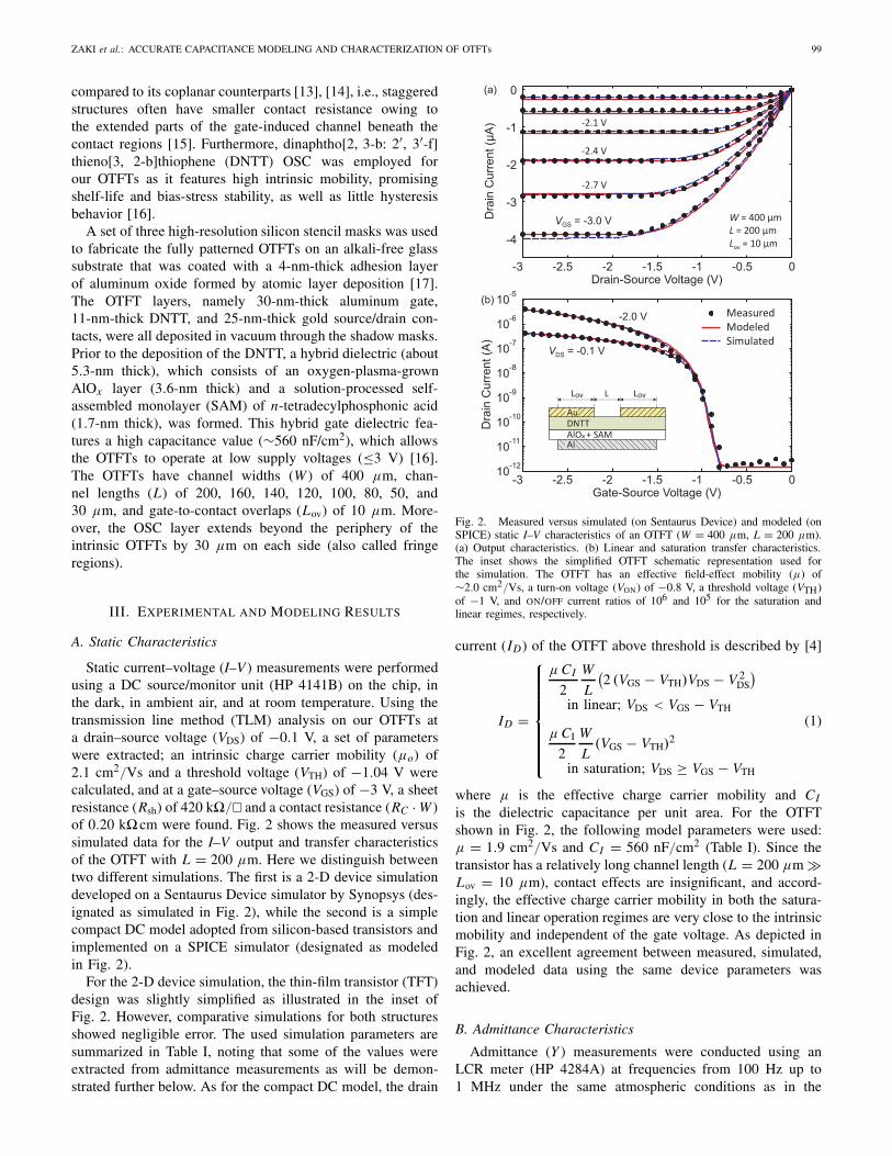
Static current–voltage (I–V ) measurements were performedusing a DC source/monitor unit (HP 4141B) on the chip, inthe dark, in ambient air, and at room temperature. Using thetransmission line method (TLM) analysis on our OTFTs ata drain–source voltage (VDS) of −0.1 V, a set of parameterswere extracted; an intrinsic charge carrier mobility (μo) of2.1 cm2/Vs and a threshold voltage (VTH) of −1.04 V werecalculated, and at a gate–source voltage (VGS) of −3 V, a sheetresistance (Rsh) of 420 k�/� and a contact resistance (RC · W )of 0.20 k� cm were found. Fig. 2 shows the measured versussimulated data for the I–V output and transfer characteristicsof the OTFT with L = 200 μm. Here we distinguish betweentwo different simulations. The first is a 2-D device simulationdeveloped on a Sentaurus Device simulator by Synopsys (des-ignated as simulated in Fig. 2), while the second is a simplecompact DC model adopted from silicon-based transistors andimplemented on a SPICE simulator (designated as modeledin Fig. 2).
For the 2-D device simulation, the thin-film transistor (TFT)design was slightly simplified as illustrated in the inset ofFig. 2. However, comparative simulations for both structuresshowed negligible error. The used simulation parameters aresummarized in Table I, noting that some of the values wereextracted from admittance measurements as will be demon-strated further below. As for the compact DC model, the drain
Fig. 2. Measured versus simulated (on Sentaurus Device) and modeled (onSPICE) static I–V characteristics of an OTFT (W = 400 μm, L = 200 μm).(a) Output characteristics. (b) Linear and saturation transfer characteristics.The inset shows the simplified OTFT schematic representation used forthe simulation. The OTFT has an effective field-effect mobility (μ) of∼2.0 cm2/Vs, a turn-on voltage (VON) of −0.8 V, a threshold voltage (VTH)of −1 V, and ON/OFF current ratios of 106 and 105 for the saturation andlinear regimes, respectively.
current (ID) of the OTFT above threshold is described by [4]
ID =
⎧⎪⎪⎪⎪⎪⎪⎪⎨
⎪⎪⎪⎪⎪⎪⎪⎩
μ CI
2
W
L
(2 (VGS − VTH)VDS − V 2
DS
)
in linear; VDS < VGS − VTH
μ CI
2
W
L(VGS − VTH)2
in saturation; VDS ≥ VGS − VTH
(1)
where μ is the effective charge carrier mobility and CI
is the dielectric capacitance per unit area. For the OTFTshown in Fig. 2, the following model parameters were used:μ = 1.9 cm2/Vs and CI = 560 nF/cm2 (Table I). Since thetransistor has a relatively long channel length (L = 200 μm �Lov = 10 μm), contact effects are insignificant, and accord-ingly, the effective charge carrier mobility in both the satura-tion and linear operation regimes are very close to the intrinsicmobility and independent of the gate voltage. As depicted inFig. 2, an excellent agreement between measured, simulated,and modeled data using the same device parameters wasachieved.
B. Admittance Characteristics
Admittance (Y ) measurements were conducted using anLCR meter (HP 4284A) at frequencies from 100 Hz up to1 MHz under the same atmospheric conditions as in the

100 IEEE TRANSACTIONS ON ELECTRON DEVICES, VOL. 61, NO. 1, JANUARY 2014
TABLE I
SIMULATION AND MATERIAL PARAMETERS
static measurements. The capacitance (C) and the conduc-tance (G) were calculated using equations C = Im(Y/ω) andG = Re(Y ), respectively, where ω is the angular frequency.To initially extract CI , dedicated metal–insulator–metal (MIM)devices with different dimensions (200 × 200, 100 × 100,50 × 50, and 10 × 10 μm2) were fabricated on the samesubstrate. In principle, the MIM is a two-terminal pendantof the OTFT sharing the same layer structure except for thesemiconductor. The average value measured for the MIMs withdifferent areas was found to be CI = 560 nF/cm2 (Table I).With the hybrid insulator thickness of about dis = 5.3 nm, aneffective value of εis = 3.37 resulted for the relative dielectricconstant.
Fig. 3 shows the capacitance–voltage (C–V ) curves of theOTFT with L = 200 μm calculated from the measuredadmittance. For this setup, the source and drain contactswere electrically shorted and connected to the low terminal(virtual ground) of the LCR meter, while the gate electrodewas connected to the high terminal. A DC potential sweepfrom zero to −3 V along with a superimposed AC voltage(Vm) of ±100 mV was applied to the gate. The C–V curvesshow a typical transition from depletion (at low absolutebias potential) to accumulation (at higher negative voltages),determined by the doping concentration of the semiconductor(Table I). Note that, as the frequency increases, the accu-mulated charges in the gate-induced channel cannot followthe signal. Considering the measurement at the frequency off = 500 Hz, a maximum capacitance of Cmax = 566 pF (inaccumulation) and a minimum capacitance of Cmin = 13 pF(in depletion) were measured. The value of Cmin correspondsto the overlap capacitances (2 · Cov) between the gate andthe source/drain contacts and can be modeled as a seriessum of two dielectrics (with εis = 3.37 for the hybrid gatedielectric and εDNTT = 2.84 for the fully depleted layerof DNTT). On the other hand, the Cmax is the geometricalcapacitance between the gate and the channel and it is simplygiven by the hybrid dielectric capacitance per unit area CI ,while taking into consideration that the gate-induced channelextends beyond the periphery of the intrinsic OTFT through
Fig. 3. Measured versus simulated capacitance–voltage (C–V ) characteristicsof an OTFT (W = 400 μm, L = 200 μm) as a function of gate bias and atdifferent frequencies. The inset shows the used measurement setup, where thedevice under test (DUT) is the p-channel OTFT. The dashed line representsthe simulations, assuming a mobility of μ = 2.0 cm2/Vs and a contributionof the fringe part of about 13%. Note that the simulations also fit well to theconductance–voltage (G–V ) characteristics (not shown here).
both the overlaps and the fringe regions. The pronouncedratio between the measured capacitances in the depletionand the accumulation modes (×44) is due to the patterningof the gate layer and the use of a relatively small gateoverlap (Lov = 10 μm � L = 200 μm) [11]. This helps inmodeling the OTFT intrinsic capacitances accurately. Fur-thermore, Fig. 3 shows the results of the device simulation.At f = 500 Hz, the transition slope between accumulationand depletion is determined only by an unintentional doping(NA). From the minimum capacitance, the effective layerthickness (d) of the OSC was estimated. At this frequency, themeasured curve was well described with NA = 1016 cm−3 andd = 11 nm (Table I) with the exception of the transi-tion region near −1 V; however, the error in this regionis less than 10% and probably caused by the large volt-age step in the measurement. To simulate correctly the flatband voltage a concentration of fixed interface charges ofNif = 1.1 × 1012 cm−2 was assumed. The frequency depen-dence of the C–V curves was well simulated by consideringa mobility of μ = 2.0 cm2/Vs for the injected holes from thesource/drain electrodes. For the highest frequencies (40 kHzand 1 MHz), a smaller contribution of the fringe part shouldbe assumed to reduce the error. Nevertheless, the value of themobility corresponds very well with the aforementioned TLMmeasurements and static simulation.
C. Frequency Response Analysis
To investigate the charge response behavior, the capacitanceand the loss (G/ω) of the OTFT with L = 200 μm weremeasured as a function of frequency (Fig. 4). Similar to theprevious setup (Fig. 3), the results include the intrinsic as wellas the parasitic OTFT components, i.e., the fringe and overlapregions. Above threshold, the holes appear to respond well tothe applied small signal up to a certain frequency dependingon the gate potential; however, their responsiveness starts todegrade above this frequency due to limited lateral flow ofholes [11]. At the said frequency, also referred to as relaxationor cutoff frequency ( fc), the measured capacitance decreasesand the loss reaches a maximum. This kind of dispersion

ZAKI et al.: ACCURATE CAPACITANCE MODELING AND CHARACTERIZATION OF OTFTs 101
Fig. 4. Measured versus modeled admittance of an OTFT (W = 400 μm,L = 200 μm) as a function of frequency and at different gate biases.(a) Capacitance–frequency (C– f ) characteristics, where C = Im(Y/ω).(b) Loss–frequency (G/ω– f ) characteristics, where G = Re(Y ). The OTFTsmall-signal equivalent circuit model is depicted in the inset.
occurs as a result of the frequency- and voltage-dependentaccumulation layer, while another dispersion is expected tooccur above 1 MHz due to the overlap regions. For the lattercase, the measured capacitances fall to zero.
A small-signal equivalent circuit was developed to explainthe conduction mechanism and quantitatively evaluate theimpact of the parasitic impedances. As depicted in the inset ofFig. 4, the model consists of a distributed circuit with parasiticresistances at the contact [8]–[11]. The channel and the fringeregions act as an RC transmission line owing to the distributedcoupling between the gate electrode and the semiconductor.From the geometry, the contribution of the fringe part wasfound to be about 16.5%.
In total, the model consists of five parameters: source/draincontact resistances (RS,D), channel resistance per unitlength (rch), dielectric capacitance per unit length (ci ), andsemiconductor capacitance per unit length (cs). The resistancesRS,D = RC/2 [�] and rch = Rsh/W [�/cm] were directlyobtained from the TLM measurements. Since there is nopotential difference between the drain and source electrodesduring this measurement, rch was assumed to be uniformalong the whole channel. In accumulation, the influence of thesemiconductor capacitance was negligible (cs � ci ). In deple-tion, the capacitance cs governs the change in the depletionlayer thickness depending on the gate voltage. Finally, thecapacitance ci = CI · W [F/cm] was acquired from the capac-itance measurements of the MIM structures. At VGS = −3 V,
Fig. 5. Measured versus modeled admittance of several OTFTs(W = 400 μm, L = 200, 160, 140, 120, 100, 80, 50, and 30 μm) as afunction of frequency and at a gate bias of VGS = −3 V. (a) Capacitance–frequency (C– f ) characteristics, where C = Im(Y/ω). (b) Loss–frequency(G/ω– f ) characteristics, where G = Re(Y ). Note that the model (shown inthe inset of Fig. 4) here used a constant set of parameters except for thechannel length (L).
the following values were used: RC · W = 0.24 k� cm,Rsh = 500 k�/�, and CI = 560 nF/cm2 (there is only aslight difference of <20% to the values extracted from TLM).As shown in Fig. 4, the model shows good agreement withboth the capacitance and loss of the measured admittance overthe complete frequency range (100 Hz–1 MHz).
Furthermore, the measured admittance at VGS = −3 Vfor all the fabricated OTFTs with channel lengths ofL = 200, 160, 140, 120, 100, 80, 50, and 30 μm wascompared with the small-signal equivalent circuit as shownin Fig. 5. A reliable and precise fit of the model to theexperimental data was obtained. The measurements shown inFigs. 4(b) and 5(b) verify that the cutoff frequency, which wasestimated at the peak of G/ω, increases with decreasing chan-nel length and with increasing gate bias. This approximatelyconforms with the expression fc � μ(VGS −VTH)/(2π L2) [8].
The dynamic performance of the intrinsic OTFT can beestimated by the response time of the gate-induced chargesin the channel [9]. Evaluation of the RC transmission linemodel (Fig. 4) of the channel in [18] has yielded the followingexpressions for the gate-to-channel capacitance (Cch) and loss(Gch/ω):
Cch = CI W L
α·(
sinh α + sin α
cosh α + cos α
)
(2)
Gch
ω= CI W L
α·(
sinh α − sin α
cosh α + cos α
)
(3)

102 IEEE TRANSACTIONS ON ELECTRON DEVICES, VOL. 61, NO. 1, JANUARY 2014
Fig. 6. (a) Calculated effective delay (τ ) for 97% of the total charges inthe OTFT channel to be induced and effectively responding. (b) NormalizedC–V measurements at f = 10 kHz. The contribution of the fringe part wasassumed to be constant (16.5%) for all channel lengths, and the normalizationwas done by dividing the measurement results by 1.165 CIW (L+2Lov). Thereis an error of < 3% because of this assumption.
where α = √ωCI Rsh L2/2. A delay time (τ ), needed for 97%
(when α = 1) of the total charges in the channel to be inducedand effectively responding, is accordingly determined as τ =1/ω = RshCI L2/2 (the relation is slightly different from theone given in [9] because of the different device structure used).Fig. 6(a) shows the calculated τ as a function of L usingthe same modeling parameters Rsh = 500 k�/� and CI =560 nF/cm2, from which information about the maximum fachieved for a given minimum L and/or maximum L neededfor a given f can be deduced. For example, one can estimatefrom Fig. 6(a) that for operation at f = 10 kHz, the OTFTsshould have L ≤ 106 μm. This corresponds closely with thenormalized C–V measurements of the OTFTs at 10 kHz asdepicted in Fig. 6(b).
D. Meyer’s Capacitance Model
In principle, the application of a drain–source bias to theOTFT results in a nonuniform distribution of charges alongthe channel. An accurate description of this effect requires adistributed capacitance model, which can in practice be simpli-fied into lumped capacitive elements between the source, drain,and gate terminals. In this case, the resulting errors in circuitsimulations are typically small [19]. We have been consideringso far admittance measurements with shorted source and draincontacts; however, a different setup was used here to account
Fig. 7. Measured gate–source (Cgs) and gate–drain (Cgd) capacitances alongwith modeled and simulated results of an OTFT (W = 400 μm, L = 200 μm).(a) Cgs and Cgd as a function of VDS. (b) Cgs and Cgd as a function ofVGS. Note that the modeled curves are represented by (4) and (5), which arevalid above threshold (solid lines). The voltage-dependent fringe factor of thesimulated curves was calculated by dividing the measured value of Cgs bythe simulated intrinsic value. The inset shows the used measurement setup.
for the variations in the stored charges of the OTFT at differentVDS and VGS. Accordingly, the gate electrode was connected tothe low terminal of the LCR meter, while the source and draincontacts were connected alternatively to the high terminal ofthe LCR meter and a DC voltage source [11]. The DC voltagesVDS and VGS were both swept from zero to −3 V, and an ACsignal of ±100 mV with f = 500 Hz was applied to eitherthe source or the drain.
Fig. 7 shows the measured gate–source (Cgs) and gate–drain (Cgd) capacitances along with modeled and simulatedresults for the OTFT with L = 200 μm. Again, the datainclude both the intrinsic and parasitic components. Similarto the previous measurements, the parasitic component iscomposed of about 16.5% for the fringe region and a constant6.5 pF (Cov) for each of the gate–source and gate–drainoverlap areas. By excluding the parasitic components, itwas found that Cgs = Cgd = 1/2 Cch at VDS = 0 V,while Cgs and Cgd approach 2/3 Cch and zero, respectively,at VDS > VGS − VTH (saturation regime). This charge storageeffect complies with Meyer’s capacitance model, which wasdeveloped originally for silicon-based MOSFETs [12]. More-over, the result indicates that a small change in the applied VDS
when the channel is pinched off during saturation regime doesnot have an impact on the gate or channel charges; however,the channel is completely assigned to the source terminal,resulting in a maximum value for Cgs [19].

ZAKI et al.: ACCURATE CAPACITANCE MODELING AND CHARACTERIZATION OF OTFTs 103
According to the Meyer’s capacitance model, the distributedintrinsic capacitances Cgs and Cgd above threshold are givenby [12], [19]
Cgs = ∂ QG
∂VGS
����VGD
= 2
3CI W L
�1 −
�VGT − VDSe
2VGT − VDSe
�2�
(4)
Cgd = ∂ QG
∂VGD
����VGS
= 2
3CI W L
�1 −
�VGT
2VGT − VDSe
�2�
(5)
where VGT = VGS−VTH, and VDSe is the effective drain–sourcevoltage that is equal to VDS for VDS < VGT and is equal to VGT
for VDS > VGT. VDSe is actually used to avoid discontinuity atthe onset of the saturation region and it is expressed as [19]
VDSe = 1
2
�VDS + VGT −
�V 2
δ + (VDS − VGT)2�
(6)
where Vδ is a constant voltage that determines the width ofthe transition region. In principle, Meyer’s model does notguarantee charge conservation and there have been attemptsin [20] and [21] to derive other models for the OTFTsintrinsic capacitances. However, we preferred to use here thesimple Meyer’s model because the resulting errors in circuitsimulations are usually small. Using CI = 580 nF/cm2,VTH = −1.18 V, and Vδ = 0.1 V, in addition to multiplyingboth (4) and (5) by 1.165 for the fringe region and adding6.5 pF for the overlap capacitance (Cov), a precise fit betweenthe modeled and measured data was accomplished as depictedin Fig. 7.
Furthermore, the measured and modeled characteristicswere compared with the device simulation results as demon-strated in Fig. 7. Using the same simulation parameters givenin Table I, excellent agreement for all voltage regions wasobtained for both Cgs and Cgd. It was necessary here to includea voltage-dependent fringe factor because otherwise the resultswere not well described. The reason is simply the smallerinfluence of fringe effects for small intrinsic capacitances,which occurs in the case of the subthreshold or the linearoperation regions.
IV. CONCLUSION
Frequency response analysis on top-contact OTFTs basedon DNTT by means of admittance measurements were per-formed. A small-signal equivalent circuit based on a dis-tributed transmission line model was used to produce agood fit to the data for different operating frequencies(100 Hz–1 MHz), biasing potentials (−3 V to zero), andchannel lengths (30–200 μm). Material parameters extractedfrom the dynamic C–V measurements were similar to theones obtained from the static I–V characteristics, except forthe density of fixed interface states, which was due to thenegative bias stress imposed during the dynamic measure-ments. Moreover, the charge storage behavior in the OTFTwas very well described by 2-D simulation as well as compactmodeling. The dependence of the intrinsic capacitances Cgs
and Cgd on the applied voltages VGS and VDS showed excellentagreement with Meyer’s capacitance model, which can inprinciple be easily incorporated into a SPICE simulator. Allthe necessary parameters employed by the simulation and
modeling conformed closely to the values extracted from thestatic measurements.
ACKNOWLEDGMENT
The authors would like to thank Prof. K. Takimiya,Hiroshima University, Japan, for providing the organic semi-conductor DNTT.
REFERENCES
[1] H. Sirringhaus, “Materials and applications for solution-processedorganic field-effect transistors,” Proc. IEEE, vol. 97, no. 9,pp. 1570–1579, Sep. 2009.
[2] M. C. J. M. Vissenberg and M. Matters, “Theory of the field-effectmobility in amorphous organic transistors,” Phys. Rev. B, vol. 57, no. 20,pp. 12964–12967, May 1998.
[3] A. R. Brown, C. P. Jarret, D. M. de Leeuw, and M. Matters,“Field-effect transistors made from solution-processed organic semicon-ductors,” Synth. Met., vol. 88, no. 1, pp. 37–55, Apr. 1997.
[4] O. Marinov, M. Deen, U. Zschieschang, and H. Klauk, “Organic thin-film transistors: Part I—Compact DC modeling,” IEEE Trans. ElectronDevices, vol. 56, no. 12, pp. 2952–2961, Dec. 2009.
[5] T. Zaki, R. Rödel, F. Letzkus, H. Richter, U. Zschieschang, H. Klauk,et al., “S-parameter characterization of submicrometer low-voltageorganic thin-film transistors,” IEEE Electron Device Lett., vol. 34, no. 4,pp. 520–522, Apr. 2013.
[6] T. Zaki, R. Rödel, F. Letzkus, H. Richter, U. Zschieschang, H. Klauk,et al., “AC characterization of organic thin-film transistors with asym-metric gate-to-source and gate-to-drain overlaps,” Org. Electron., vol. 14,no. 5, pp. 1318–1322, May 2013.
[7] D. M. Taylor, D. L. John, and J. A. Drysdale, “Frequency-response ofthe accumulation channel in organic MISFETs,” in Proc. Mater. Res.Soc. Symp., Apr. 2007, pp. 104–111.
[8] T. Miyadera, T. Minari, K. Tsukagoshi, H. Ito, and Y. Aoyagi,“Frequency response analysis of pentacene thin-film transistors with lowimpedance contact by interface molecular doping,” Appl. Phys. Lett.,vol. 91, no. 1, pp. 013512-1–013512-3, Aug. 2007.
[9] K.-D. Jung, C. A. Lee, D.-W. Park, B.-G. Park, H. Shin, andJ. D. Lee, “Admittance measurements on OFET channel and its modelingwith R − C network,” IEEE Electron Device Lett., vol. 28, no. 3,pp. 204–206, Mar. 2007.
[10] D. M. Taylor and N. Alves, “Separating interface state responsefrom parasitic effects in conductance measurements on organic metal-insulator-semiconductors capacitors,” J. Appl. Phys., vol. 103, no. 5,pp. 054509-1–054509-6, Mar. 2008.
[11] K. Kim and Y. Kim, “Intrinsic capacitance characteristics of top-contactorganic thin-film transistors,” IEEE Trans. Electron Devices, vol. 57,no. 9, pp. 2344–2347, Sep. 2010.
[12] J. E. Meyer, “MOS models and circuit simulation,” RCA Rev., vol. 32,no. 1, pp. 42–63, Mar. 1971.
[13] D. J. Gundlach, L. Zhou, J. A. Nichols, T. N. Jackson,P. V. Necliudov, and M. S. Shur, “An experimental study of contacteffects in organic thin film transistors,” J. Appl. Phys., vol. 100, no. 2,pp. 024509-1–024509-13, Jul. 2006.
[14] C. H. Shim, F. Maruoka, and R. Hattori, “Structural analysis on organicthin-film transistor with device simulation,” IEEE Trans. ElectronDevices, vol. 57, no. 1, pp. 195–200, Jan. 2010.
[15] F. Ante, D. Kälbein, T. Zaki, U. Zschieschang, K. Takimiya, M. Ikeda,et al., “Contact resistance and megahertz operation of aggressivelyscaled organic transistors,” Small, vol. 8, no. 1, pp. 73–79, Jan. 2012.
[16] U. Zschieschang, F. Ante, D. Kälblein, T. Yamamoto, K. Takimiya,H. Kuwabara, et al., “Dinaphtho[2, 3-b: 2′, 3′-f]thieno[3, 2-b]thiophene(DNTT) thin-film transistors with improved performance and stability,”Org. Electron., vol. 12, no. 8, pp. 1370–1375, Aug. 2011.
[17] F. Ante, F. Letzkus, J. Butschke, U. Zschieschang, K. Kern,J. N. Burghartz, et al., “Submicron low-voltage organic transistors andcircuits enabled by high-resolution silicon stencil masks,” in Proc. IEEEIEDM, Dec. 2010, pp. 21.6.1–21.6.4.
[18] D. W. Greve and V. R. Hay, “Interpretation of capacitance-voltagecharacteristics of polycrystalline silicon thin-film transistors,” J. Appl.Phys., vol. 61, no. 3, pp. 1176–1180, Feb. 1987.

104 IEEE TRANSACTIONS ON ELECTRON DEVICES, VOL. 61, NO. 1, JANUARY 2014
[19] T. Ytterdal, Y. Cheng, and T. Fjeldly, Device Modeling for Analog andRF CMOS Circuit Design. Chichester, U.K.: Wiley, 2003.
[20] A. Castro-Carranza, M. Estrada, J. Nolasco, A. Cerdeira, L. Marsal,B. Iniguez, et al., “Organic thin-film transistor bias-dependent capac-itance compact model in accumulation regime,” IET Circuits, DevicesSyst., vol. 6, no. 2, pp. 130–135, Mar. 2012.
[21] O. Marinov and M. J. Deen, “Quasistatic compact modelling of organicthin-film transistors,” Org. Electron., vol. 14, no. 1, pp. 295–311,Jan. 2013.
Tarek Zaki (S’07) received the B.Sc. (HighestHons.) and M.Sc. (Distinction) degrees in electronicsengineering from the German University in Cairo(GUC), Cairo, Egypt, and the University of Stuttgart,Stuttgart, Germany, in 2009 and 2010, respectively.He is currently pursuing the Ph.D. degree at theUniversity of Stuttgart.
Susanne Scheinert received the Ph.D. degree inelectrical engineering from the Ilmenau Universityof Technology, Ilmenau, Germany, in 1992. She hasbeen the Head of the Solid State Electronics Group,Ilmenau University of Technology, since 1999. Herresearch focuses on organic field effect transistors.
Ingo Hörselmann received the Diploma degree inelectrical engineering from the Ilmenau Universityof Technology, Ilmenau, Germany, in 2003. Hiscurrent research interests include numeric simulationand dynamic behavior of OTFTs, under the leader-ship of PD Dr. S. Scheinert.
Reinhold Rödel received the Diploma degree innanotechnology from the University of Würzburg,Würzburg, Germany, in 2010. He is currently pur-suing the Ph.D. degree in physics from the SwissFederal Institute of Technology in Lausanne (EPFL),Lausanne, Switzerland.
Florian Letzkus received the master’s degree inphysics from the University of Tübingen, Tübin-gen, Germany, and the Ph.D. degree from the Uni-versity of Stuttgart, Stuttgart, Germany, in 1996and 2003, respectively. He is currently heading theNanoprocess Department, IMS CHIPS, Stuttgart.
Harald Richter received the Ph.D. degree in physicsfrom the University of Stuttgart, Stuttgart, Germany,in 1983. He was with XRCW and at MPI-FKFbefore joining IMS CHIPS in 1986. Since 2005, hehas been the Head of the System Division, wherehe is responsible for CMOS imagers and ASICdevelopment.
Ute Zschieschang received the Ph.D. degreein chemistry from the Technical UniversityBergakademie Freiberg, Freiberg, Germany, in2006. She has been a Scientist with the OrganicElectronics Group, Max Planck Institute for SolidState Research, Stuttgart, Germany, since 2005.
Hagen Klauk (S’97–M’99) received the Ph.D.degree in electrical engineering from the Pennsyl-vania State University, State College, PA, USA, in1999. He was with Infineon Technologies, Neu-biberg, Germany, from 2000 to 2005. In 2005, hejoined the Max Planck Institute for Solid StateResearch, Stuttgart, Germany.
Joachim N. Burghartz (M’90–SM’92–F’02)received the Dipl.Ing. and Ph.D. degrees inelectrical engineering from RWTH Aachen,Aachen, Germany, and the University of Stuttgart,Stuttgart, Germany, in 1982 and 1987, respectively.He is the Director of IMS CHIPS, Stuttgart, and aFull Professor with the University of Stuttgart.