ieee transactions on power electronics, …mazumder/hybrid_modulation.pdfieee transactions on power...
TRANSCRIPT
IEEE TRANSACTIONS ON POWER ELECTRONICS, VOL. 31, NO. 1, JANUARY 2016 861
Hybrid Modulation Scheme for a High-FrequencyAC-Link Inverter
Sudip K. Mazumder, Senior Member, IEEE
Abstract—This paper describes a hybrid modulation scheme fora high-frequency ac-link (HFACL) multistage inverter comprisinga front-end dc/ac converter, followed by isolation transformers,an ac/pulsating-dc converter, and a pulsating-dc/ac converter. Thehybrid modulation scheme enables 1) removal of the dc-link fil-ter evident in conventional fixed dc-link (FDCL) inverters placedafter the ac/pulsating-dc converter stage and before an end stagevoltage source inverter and 2) significant reduction in switchingloss of the inverter by reducing the high-frequency switching re-quirement of the pulsating-dc/ac converter by two-third yieldinghigher efficiency, improved voltage utilization, and reduced currentstress. Unlike the FDCL approach, in the HFACL approach, hy-brid modulation enables the retention of the sine-wave-modulatedswitching information at the output of the ac/pulsating-dc con-verter rather than filtering it to yield a fixed dc thereby reducingthe high-frequency switching requirement for the pulsating-dc/acconverter. Overall, the following is outlined: 1) hybrid modulationscheme and its uniqueness, 2) operation of the HFACL inverter us-ing the hybrid modulation scheme, 3) comparison of the efficiencyand losses, current stress, and harmonic distortion between thehybrid-modulation-based HFACL inverter and the FDCL inverter,and 4) scaled experimental validation. It is noted that the term hy-brid modulation has no similarity with the modulation scheme for ahybrid converter (which are conjugation of two types of convertersbased on a slow and fast device) reported in the literature. The termhybrid modulation scheme is simply chosen because at any giventime only one leg of the inverter output stage (i.e., pulsating-dc/acconverter) switch under high frequency, while the other two legsdo not switch. The outlined hybrid modulation scheme is unlikeall reported discontinuous modulation schemes where the input isa dc and not a pulsating modulated dc, and at most only one legstays on or off permanently in a 60° or 120° cycle.
Index Terms—AC link, high frequency, hybrid modulation,inverter, isolation, loss, reachability.
I. INTRODUCTION
S I-DEVICE-BASED high-power inverters usually operate atlow switching frequencies owing to higher switching loss
and thermal limitations of Si. Low switching frequency yieldsbulky and expensive magnetic and capacitive filter elements orcomplex topological structure (for a given device breakdownvoltage) to attain higher commutation frequency for the samedevice switching frequency. If isolation is required, conven-tional transformer core materials also yield heavier, costlier,
Manuscript received October 5, 2014; revised December 13, 2014; acceptedMarch 5, 2015. Date of publication March 10, 2015; date of current versionSeptember 21, 2015. This work was supported in part by the U.S. NationalScience Foundation under Awards 0725887, 1002369, and 1239118. Recom-mended for publication by Associate Editor A. M. Trzynadlowski.
S. K. Mazumder is with the Laboratory for Energy and Switching-ElectronicsSystems, Department of Electrical and Computer Engineering, University ofIllinois, Chicago, IL 60607, USA (e-mail: [email protected]).
Color versions of one or more of the figures in this paper are available onlineat http://ieeexplore.ieee.org.
Digital Object Identifier 10.1109/TPEL.2015.2411714
and high-footprint space device. Recently, developed SiC MOS-FETs (with 100–400X lower on resistance) and SiC Schottkydiodes (with superior reverse recovery) [1], [2] with high ther-mal conductivity and thermal sustenance, and high permeabilityand efficient nanocrystalline-core-based transformers [3], [4]overcome some of these limitations. Clearly, they pave wayfor compact isolated high-power and high-frequency systemsand have attained significant attention with regard to applica-tions including renewable and alternative energy-based systems,fuel cell and energy storage applications, active filters, tractiondrives, and solid-state transformers because of potential for sub-stantial reduction in materials and labor cost without significantcompromise in efficiency.
Towards that goal, two high-frequency topologies have re-ceived attention [5]–[13]. The first topology, as shown in Fig. 1,will be referred refer to as the high-frequency ac-link (HFACL)topology. The second topology, which is referred in this pa-per as the fixed dc-link (FDCL) topology is obtained fromFig. 1 by simply placing a dc-link capacitor at the output ofthe ac/pulsating-dc converter. Both the topologies have a front-end high-frequency dc/ac converter followed by an ac/pulsating-dc converter and support galvanic isolation. However, the twotopologies differ at the output stage. The output stage of theFDCL topology is a dc/ac voltage source inverter (VSI) that ispreceded by a decoupling link capacitor. While the last stageof the HFACL topology is a pulsating-dc/ac converter, whichis not preceded by any decoupling link capacitor. Furthermore,for the HFACL topology, the dc/ac converter is operated withsine wave modulation, while the pulsating-dc/ac converter isoperated with hybrid modulation. For the FDCL topology, thedc/ac converter operates with square wave modulation and thefinal stage dc/ac converter (i.e., VSI) is sinusoidally modulated.
In the context of the HFACL inverter topology, a new in-novation in the form of a hybrid modulation [5], [6] has beenput forward by the author that significantly reduces the switch-ing loss of the HFACL topologies (e.g., Fig. 1). This modulationscheme is unlike all reported discontinuous modulation schemes[14] where the input is a dc and not a pulsating modulated dc,and at most only one leg stays on or off permanently in a 60° or120° cycle. The present three-phase hybrid modulation schemeis also different from earlier reported modulation schemes forsingle-phase direct power conversion systems [15]. The primaryrole of the modulation scheme for the single-phase pulsating-dc/ac converter is to demodulate the ac/pulsating-dc converteroutput on a half-line cycle basis to generate the output sine wavemodulation pattern. This is different than the hybrid modulationscheme for the HFACL topology (see Fig. 1), where not all thelegs modulate uniformly since the output of the ac/pulsating-dc
0885-8993 © 2015 IEEE. Personal use is permitted, but republication/redistribution requires IEEE permission.See http://www.ieee.org/publications standards/publications/rights/index.html for more information.

862 IEEE TRANSACTIONS ON POWER ELECTRONICS, VOL. 31, NO. 1, JANUARY 2016
Fig. 1. Topology of an HFACL inverter. An FDCL topology has the same architecture except that it has a dc-link filter capacitor after the ac/pulsating-dcconverter, and hence, the output stage (which operates as a VSI instead of as a pulsating-dc/ac converter) is fed with a dc voltage rather than a pulsating dc voltage(Vrec ) for the HFACL scheme. The hybrid modulation scheme evaluated in this paper for the HFACL topology is implemented for the pulsating-dc/ac converterstage. For the FDCL topology, the output stage dc/ac converter (VSI) is operated using other modulation scheme. To ascertain the effectiveness of the hybridmodulation scheme, the dc/ac converter is operated with the same sinusoidal PWM technique for both HFACL and FDCL inverter topologies. The ac/pulsating-dcconverter simply rectifies the bipolar transformer secondary voltages.
Fig. 2. Diagram of gate drive signal generation for the HFACL inverter.
converter contains encoded information of only one phase-to-phase voltage output of the primary-side high-frequency dc/acconverter.
Finally, the term hybrid modulation has no similarity withthe modulation scheme for hybrid converter as reported in [16].Hybrid converters are conjugation of two types of converters thatare based on two different types of devices: one that supportshigher power and switches at slow frequency and the other thatoperates at high frequency and supports lower harmonic power.The pulsating-dc/ac converter in Fig. 1 is a single converter.The term hybrid modulation scheme simply is chosen becauseat any given time (and as demonstrated in Section II), only oneleg of the pulsating-dc/ac converter carries out forced switchingwhile the switches in the other two legs do not change theirswitching states. This effectively yields a two-third reduction
in the switching loss of the pulsating-dc/ac converter simply bymodulation and without requiring any complex circuitry.
II. OVERVIEW OF THE HYBRID MODULATION SCHEME
AND HFACL INVERTER OPERATION
The key concept regarding the operation of the hybrid modu-lation scheme relates to the evolution of the switching sequencesof the output stage pulsating-dc/ac converter given the pulsatingdc-link voltage waveform at the output of the ac/pulsating-dcrectifier. This pulsating dc-link voltage, in turn, evolves fromthe bipolar, high-frequency, and sinusoidally modulated outputvoltage waveforms of the front-end high-frequency dc/ac con-verter. Given that the dc/ac converter is modulated sinusoidally,the pulsating dc link voltage retains the sinusoidally encoded

MAZUMDER: HYBRID MODULATION SCHEME FOR A HIGH-FREQUENCY AC-LINK INVERTER 863
Fig. 3. Key waveforms of the primary dc/ac converter in one cycle and enlarged view of the interval between two dot lines: (a) three-phase sine wave references(Ref_a, Ref_b, and Ref_c) and carrier signal; (b) Q: square ware with half frequency of the carrier; (c) UT: gate signal for the upper switch of phase U; (d) VT:gate signal for the upper switch of phase V; (e) Vuv : output of phase U and V; and (f) Vrec : output waveform of the rectifier.
information of two active phases of the dc/ac converter becauseonly the maximum phase-to-phase voltage of the dc/ac con-verter feeds the ac/pulsating-dc converter. As such, to create abalanced three-phase output using this pulsating dc-link voltageat the output of the pulsating-dc/ac converter, while two legsof the latter do not change switching states at all, the third leghas to be switched to reconstruct the remaining output phases.The choice of the two legs that do not change switching stateschanges every 60° of the 60-Hz line cycle. This is because every60°, a new dc/ac converter phase-to-phase voltage attains thepeak voltage. In addition to that, two additional issues need tobe resolved: for the two legs of the pulsating-dc/ac converterthat do not change switching states, what should be the switch-ing state of each leg during the 60° period; and how should oneswitch the third leg of the pulsating-dc/ac converter that oper-ates at high frequency. All of these have been outlined below inthis section.
Fig. 2 illustrates the generation of switch gate signals forthe HFACL inverter. The bottom switches are controlled com-plimentarily to the upper ones hence they are not describedfurther. Three gate drive signals UT, VT, and WT for primary-side devices are obtained by phase shifting a square wave withrespect to a 20-kHz square wave signal Q [shown in Fig. 3(b)].Signal Q is synchronous with a 40-kHz sawtooth carrier sig-nal, as shown in Fig. 3(a). The phase differences are modu-lated sinusoidally using three 60-Hz references for phases a,b, and c. Two gate signals (for switches UT and VT) corre-sponding to phases U and V are illustrated in Fig. 3(c) and(d), respectively. Because the carrier frequency is much higherthan the reference frequency, UT, VT, and WT will be squarewave with the frequency of 20 kHz and their phases are mod-ulated. The resulting output phase-to-phase voltages at the pri-mary side of the transformers are bipolar waveforms. WaveformVuv is plotted in Fig. 3(e) as an illustration. It is noted that the

864 IEEE TRANSACTIONS ON POWER ELECTRONICS, VOL. 31, NO. 1, JANUARY 2016
Fig. 4. Key waveforms of the hybrid-modulation-based pulsating-dc/ac converter in one cycle and an enlarged view of the interval between two dotted lines: (g)Vrec : output PWM waveform of the ac/pulsating-dc converter with six pulse envelop; (h) mod: modulated signal and ramp: the carrier which is synchronous with(g); (i) UUT: gate signal for the top switch of phase a; (j) VVT: gate signal for the top switch of phase b; (k) WWT: gate signal for the top switch of phase c; and(l) PWM output of the line to line voltage Vab and its envelop.
transformer is a high-frequency transformer since the flux bal-ance is achieved at 20 kHz by using a volt–second balancedbipolar signal that ensures resetting every 50 μs. After pass-ing through high-frequency transformers, the phase-to-phasevoltage signals are rectified by the ac/pulsating-dc converter toobtain a unipolar PWM waveform, which has a six pulse as en-velop. This waveform is shown in Fig. 3(f) and the mathematicexpressions are as follows:
Vrec = N.Vdc .MAX (|UT − VT| , |VT − WT| , |WT − UT|)(1)
UT = Q ⊗ PWMa (2)
VT = Q ⊗ PWMb (3)
WT = Q ⊗ PWMc (4)
where PWMx (x = a, b, or c) denotes the binary comparatoroutput between reference and carrier for phase x. Symbol ⊗
TABLE IEDGE DEPENDENCE OF THE RECTIFIER OUTPUT ON GATE SIGNALS
P1 P2 P3 P4 P5 P6
↑Vr e c WT UT UT VT VT WT↓Vr e c VT VT WT WT UT UT
stands for XNOR operation, while N represents the transformerturns ratio. The six-pulse rectified waveform is partitioned intosix segments named P1–P6 and is shown in Fig 4(g). The risingand falling edges of Vrec are different for different segment.Fig. 3(a)’–(f)’ shows a particular time interval within segment2, where the rising and falling edges of Vrec (marked as ↑Vrec and↓Vrec) are determined by the edges of UT and VT, respectively.Other cases are summarized in Table I.
MAZUMDER: HYBRID MODULATION SCHEME FOR A HIGH-FREQUENCY AC-LINK INVERTER 865
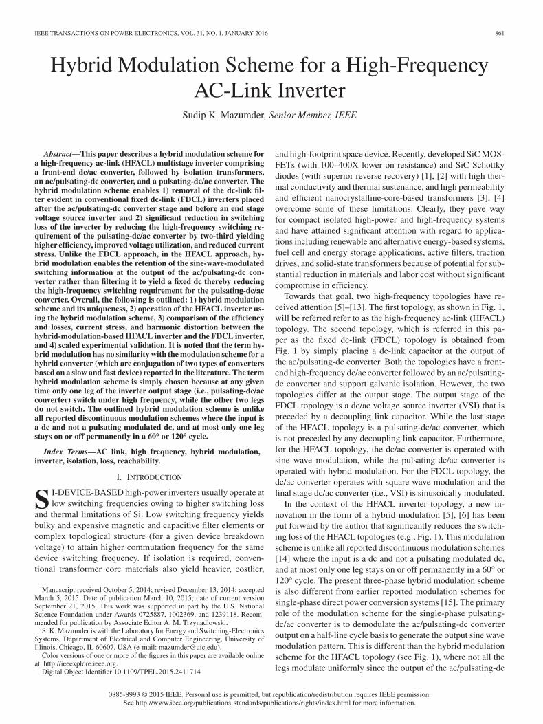
TABLE IISWITCHING PATTERN FOR UPPER SWITCHES OF THE PULSATING-DC/AC CONVERTER BASED ON HYBRID MODULATION
P1 P2 P3 P4 P5 P6
V r e c (g) Vw v Vu v Vuw Vv w Vv u Vw u
UUT (i) HF ON ON HF OFF OFFVVT (j) OFF OFF HF ON ON HFWWT (k) ON HF OFF OFF HF ONmod (h) Ab cb bc ac ca bair e c (ia + ic , ic ) or (-ib , ic ) (ia + ic , ia ) or (-ib , ia ) (ia + ib , ia ) or (-ic , ia ) (ib + ia , ib ) or (-ic , ib ) (ib + ic , ib ) or (-ia , ib ) (ic + ib , ic ) or (-ia , ic )ir e c > 0 ib < 0 < 30° lagging ia > 0 < 30° lagging ic < 0 < 30° lagging ib > 0 < 30° lagging ia < 0 < 30° lagging ic > 0 < 30° lagging
ic > 0 < 30° leading ib < 0 < 30° leading ia > 0 < 30° leading ic < 0 < 30° leading ib > 0 < 30° leading ia < 0 < 30° leading
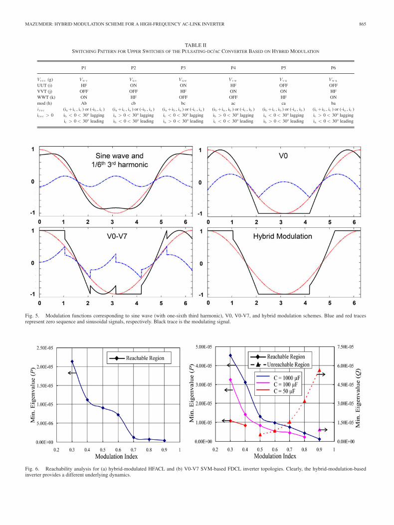
Fig. 5. Modulation functions corresponding to sine wave (with one-sixth third harmonic), V0, V0-V7, and hybrid modulation schemes. Blue and red tracesrepresent zero sequence and sinusoidal signals, respectively. Black trace is the modulating signal.
Fig. 6. Reachability analysis for (a) hybrid-modulated HFACL and (b) V0-V7 SVM-based FDCL inverter topologies. Clearly, the hybrid-modulation-basedinverter provides a different underlying dynamics.

866 IEEE TRANSACTIONS ON POWER ELECTRONICS, VOL. 31, NO. 1, JANUARY 2016
Fig. 7. Picture of the experimental inverter prototype.
TABLE IIIMAIN COMPONENTS USED IN THE EXPERIMENTAL PROTOTYPE (SYMBOL X
REPRESENTS PHASES U, V, AND W)
Name Part Number and Descriptions
X1T, X2T, X1B, X2B IPP070N06L; MOSFET, 60V/80A/6.7 mΩXT, XB SiC MOSFET, 600V/20A, Rd s (on) = 0.125 ΩDXT, DXB IDT016S60C, SiC Schottky Diode,
600V/16A/1.5 VF
Transformers Nanocrystalline core; Primary: 12T 6 x AWG14;Secondary: 52T, AWG14
As alluded to before, the PWM output of the ac/pulsating-dc converter is contributed, respectively, by Vwv , Vuv , Vuw ,Vvw , Vvu , and Vwu at each segment ranging from P1 to P6.The bottom part of the Fig. 2 shows the diagram of generatingswitching signals for three upper switches of the secondary-sidepulsating-dc/ac converter. During each segment, every switchwill be either: permanently ON (“1”), permanently OFF (“0”),or toggling with 40 kHz (“HF”). The switching pattern for theupper three switches in each segment for one-cycle period issummarized in Table II. In Table II, symbols (g), (h), (i), (j), and(k) are in reference to Fig. 4.
The switch positions illustrated in Fig. 2 are for the case ofsegment P2. Since the rectifier output has the same shape asVuv within this interval, the phase-to-phase voltage Vab at theoutput side of the pulsating-dc/ac converter is directly obtainedby keeping switches UUT and VVT in ON and OFF status, re-spectively. Another phase-to-phase voltage Vcb , however, needsto be synthesized by operating switches WWT and WWB ofthe third leg at high frequency, where the modulated signal(“mod”) is the difference between references c and b, and thecarrier signal (“ramp”) is a 40-kHz sawtooth waveform synchro-nized to the pulsewidth-modulated output of the ac/pulsating-
Fig. 8. Experimental signals of the Bridge III using (a): V0-V7 modulationand (b) hybrid modulation. Waveforms from top to bottom are: gate signals forUT, VT, WT and scaled Vrec . For (b), it is evident that at any given instant onlyone switch of the pulsating-dc converter switches at high frequency.
dc converter. The key waveforms are shown in Fig. 4. Themathematic expressions for three phase-to-phase voltages are asfollows:
Vab = Vrec · (UUT − VVT) (5)
Vcb = Vrec · (WWT − VVT) (6)
Vca = Vcb − Vab . (7)
Because the high-frequency pulsating dc voltage at the outputof the ac/pulsating-dc converter is encoded with sinusoidal in-formation, only one of the pulsating-dc/ac converter legs needsto be force switched under unity power factor condition at anygiven moment. Devices of the other two legs do not changeswitching state. This considerably reduces switching losses.

MAZUMDER: HYBRID MODULATION SCHEME FOR A HIGH-FREQUENCY AC-LINK INVERTER 867
Fig. 9. (a) Output voltage of the HFACL-based inverter. (b)–(d) Output voltage and current of phases a through c.
Fig. 5 illustrates the modulation functions of the hybrid mod-ulation scheme with four well-known SVM schemes (namelysinusoidal PWM with one-sixth third harmonic injection [14]and two discontinuous SVM schemes [17], [18]: V0 and V0-V7) to illustrate that there is an underlying difference betweenthe new modulation scheme and existing ones. It is noted thatV0-V7 SVM is the minimum switching loss scheme.
Finally, by using a newly developed technique (outlinedby the author in [18]) for reachability analysis of switchingpower converters using composite Lyapunov function basedon a hybrid model, we demonstrate in Fig. 6 that the hybrid-modulation-based HFACL inverter topology is not a limitingcase of an FDCL topology for progressively reducing the dc-link capacitance. Basically, the procedure involves modelingthe HFACL and FDCL topologies using the state-space hy-
brid model x = Aix + Bi (where the matrices are functions ofthe power stage parameters in the ith switching state whichcan be easily derived following [19] and [20]), and subse-quently determining (to ascertain stability) if a matrix inequalityh∑
i=1αki
(AT
i Pki + PkiAi PkiBiBT
i Pki 0
)
< 0 is satisfied. This con-
dition, where h represents the switching states in the kth switch-ing sequence and 0 ≤ αki ≤ 1, is satisfied if matrix Pki is posi-tive definite (i.e., if the minimum eigenvalue of Pki is positive).In case this condition is not satisfied, determination of a dualmatrix Qki to be positive confirms instability. Fig. 6 clearlyshows the difference in reachability of the FDCL inverter withvoltage-sourced final stage and varying dc-link capacitance, andthe reachability of the HFACL inverter operating without the dc-link capacitance.

868 IEEE TRANSACTIONS ON POWER ELECTRONICS, VOL. 31, NO. 1, JANUARY 2016
III. RESULTS OF THE PERFORMANCE OF HYBRID MODULATION
Fig. 7 shows an experimental unit of the hybrid-modulation-based three-phase HFACL inverter. The same setup has beenused for obtaining experimental data using V0-V7 modulationfor the FDCL inverter by simply inserting a 2.2-mF dc-link ca-pacitor between ac/pulsating-dc rectifier and the output bridge.The three converter stages in Fig. 7 are identified as follows:Bridge I: (primary side) dc/ac converter; Bridge II: (secondaryside) ac/pulsating-dc converter (diode rectifier); and Bridge III:used as a pulsating-dc/ac converter for the HFACL approachor as a VSI for the FDCL approach. The basic parameter de-tails are provided in Table III. The designed input voltage ofthe inverter is 40-V dc. Transformer turns ratio is around 1:4.2.The inverter is controlled using an advanced TMS320C6713DSP and EPF10K50VRC240–2-based Xcalibur FPGA digitalcontroller boards.
Using this setup, several key experiments were conductedto analyze the performance of the hybrid modulation. To doan accurate assessment, we carry out the experiments as fol-lows. First, the dc/ac converter (Bridge I) is operated usinghigh-frequency sine wave modulation for both HFACL andFDCL approaches at 20-kHz switching frequency. Second, theac/pulsating-dc rectifier (Bridge II) is chosen to be unidirec-tional (i.e., diode based) for both the cases. Thus, up to theoutput of the Bridge II (ac/pulsating-dc converter), there is nodifference between the operation of the HFACL and FDCL in-verters. The main difference is in the final stage or Bridge III. Forthe HFACL approach, Bridge III, fed by the pulsating dc-linkvoltage, is operated as a pulsating-dc/ac converter using hybridmodulation, while for the FDCL approach, Bridge III is oper-ated as a VSI using V0-V7 modulation. This is demonstrated inFig. 8. The switching frequency of Bridge III for the FDCL ap-proach is set at 40 kHz. For the HFACL approach, the switchingfrequency is naturally set at 40 kHz because the ac/pulsating-dcconverter rectifies the Bridge I bipolar 20 kHz output, therebycreating 40-kHz pulsating dc-link signal. The output voltage ofthe HFACL-based inverter is shown in Fig. 9(a), while the outputvoltage and current of each of the three phases are demonstratedin Fig. 9(b)–(d).
Fig. 10 shows the experimental efficiency of the Bridge III us-ing hybrid modulation and V0-V7 modulation, respectively, forthe HFACL and the FDCL approaches. Clearly, hybrid modula-tion provides higher efficiency. Simulation results in Fig. 11 givean insight into the cause. As evident, compared to V0-V7 mod-ulation, hybrid modulation of Bridge III yields lower switchingloss as well as conduction loss. Reduction in the conduction lossis attributed to the reduced RMS diode and the switch currentof Bridge III, as evident in Fig. 12.
Finally, in Fig. 13, we demonstrate the experimental totalharmonic distortion (THD) of the output voltage of the hybridmodulation and V0-V7 modulation-based inverter. We observethat, although the THD using hybrid modulation is higher, it iswell within typical standard requirement of 5%. Most impor-tantly, hybrid modulation achieves such low level of THD with-out a dc-link filter that it is used for the V0-V7 FDCL scheme.It is noted further that, by operating the HFACL inverter using
Fig. 10. Experimental efficiencies of the hybrid modulation and V0-V7modulation-based Bridge III.
Fig. 11. Comparison of normalized (a) switching and (b) conduction lossesof Bridge III using hybrid modulation and V0-V7 modulation.

MAZUMDER: HYBRID MODULATION SCHEME FOR A HIGH-FREQUENCY AC-LINK INVERTER 869
Fig. 12. Comparison of normalized (a) diode and (b) switch currents of BridgeIII using hybrid modulation and V0-V7 modulation.
Fig. 13. Experimental THD of the output voltage of the hybrid modulationand V0-V7 modulation-based inverter. Symbols SPWM and PPM represent, re-spectively, sinusoidal pulse width modulation and pulse placement modulation.
a combination of pulse width and pulse placement modulationof the dc/ac converter along with the hybrid modulation of thepulsating-dc converter, one can reduce the THD of the outputvoltage to a value that is comparable to that obtained using theV0-V7 modulation [7].
IV. CONCLUSION
This paper demonstrates the performance of a hybrid-modulation-based HFACL inverter for high-power renewableand alternative-energy-based standalone, and distributed gener-ation systems. It achieves high efficiency in spite of operatingat high frequency owing to a significant reduction in switch-ing loss of the output stage pulsating-dc converter and also dueto a reduction in the conduction loss due to a net reduction inswitch and diode RMS currents. This also leads to better dc-busvoltage utilization and lesser variation in the output voltage forthe increasing load. Although the output THD is slightly higherfor the hybrid-modulation-based inverter, it is well within theacceptable level and is achieved without any bulky dc-link filter,which is used for the FDCL inverter. It is noted that, by mod-ulating the dc/ac converter based on pulse position and pulsewidth principles, the output THD of the HFACL inverter usingthe hybrid modulation is further reduced. It is also shown thatthe reachability of the hybrid-modulation-based HFACL systemis not a limiting case for the FDCL system for the progressivelyreduced dc-link capacitance.
REFERENCES
[1] H. Niwa, G. Feng, J. Suda, and T. Kimoto, “Breakdown characteristicsof 12–20 kV-class 4H-SiC PiN diodes with improved junction termina-tion structures,” in Proc. Int. Symp. Power Semicond. Devices ICs, 2012,pp. 381–384.
[2] M. K. Das, C. Capell, D. E. Grider, R. Raju, M. Schutten, J. Nasadoski,S. Leslie, J. Ostop, and A. Hefner, 10 kV, 120 A SiC half H-bridgepower MOSFET modules suitable for high frequency, medium voltageapplications,” in Proc. IEEE Energy Convers. Congress Expo., 2011,pp. 2689–2692.
[3] W. A. Reass, D. M. Baca, and R. F. Gribble, “Multi-megawatt high fre-quency polyphase nanocrystalline transformers,” presented at the HighMegawatt Converter Workshop, Nat. Inst. Standards Technol., Gaithers-burg, MD, USA, Jan. 24, 2007.
[4] G. Ortiz, M. Leibl, J. W. Kolar, and O. Apeldoorn, “Medium frequencytransformers for solid-state-transformer applications—Design and experi-mental verification,” in Proc. IEEE Int. Conf. Power Electron. Drive Syst.,2013, pp. 1285–1290.
[5] S. K. Mazumder and R. Huang, “Multiphase converter apparatus andmethod,” US Patent 7 768 800 B2, Aug. 3, 2010.
[6] S. K. Mazumder, “A novel hybrid modulation scheme for an isolatedhigh-frequency-link fuel cell inverter,” in Proc. IEEE Power Energy Soc.Gen. Meeting, 2008, pp. 1–7.
[7] S. K. Mazumder and A. Rathore, “Impact of dc link pulse coding on theharmonic distortion of the high-frequency-link inverter,” in Proc. IEEEInd. Electron. Conf., 2010, pp. 4499–504.
[8] J. Itoh, R. Oshima, and H. Takahashi, “Experimental verification of highfrequency link dc-ac converter using pulse density modulation at sec-ondary matrix converter,” in Proc. Int. Power Electron. Conf., 2014,pp. 1021–1027.
[9] S. Xu, Y. Xunwei, W. Fei, and A. Q. Huang, “Design and demonstration ofa 3.6-kV–120-V/10-kVA solid-state transformer smart grid application,”vol. 29, no. 8, pp. 3982–3996, Dec. 2013.
[10] K. Basu and N. Mohan, “A high-frequency link single-stage PWM inverterwith common-mode voltage suppression and source-based commutationof leakage energy,” IEEE Trans. Power Electron., vol. 29, no. 8, pp. 3907–3918, Sep. 2013.

870 IEEE TRANSACTIONS ON POWER ELECTRONICS, VOL. 31, NO. 1, JANUARY 2016
[11] P. Jain, M. Pahlevaninezhad, S. Pan, and J. Drobnik, “A review of high-frequency power distribution systems: for space, telecommunication, andcomputer applications,” IEEE Trans. Power Electron., vol. 29, no. 8,pp. 3852–3863, Nov. 2013.
[12] L. Chen, A. Amirahmadi, Q. Zhang, N. Kutkut, and I. Batarseh, “De-sign and implementation of three-phase two-stage grid-connected mod-ule integrated converter,” IEEE Trans. Power Electron., vol. 29, no. 8,pp. 3881–3892, Dec. 2013.
[13] H. Keyhani and H. A. Toliyat, “Single-stage multistring PV inverter withan isolated high-frequency link and soft-switching operation,” IEEE Trans.Power Electron., vol. 29, no. 8, pp. 3919–3929, Nov. 2013.
[14] D. G. Holmes and T. A. Lipo, Pulse-Width Modulation for Power Con-verters: Principles and Practice. Hoboken, NJ, USA: Wiley, 2003.
[15] B. K. Bose, P. M. Szczesny, and R. Steigerwald, “Microcomputer controlof a residential photovoltaic power conditioning system,” IEEE Trans.Ind.. Appl., vol. IA-21, no. 5, pp. 1182–1191, Sep. 1985.
[16] M. Manjrekar and T. Lipo, “Hybrid multilevel power conversion system:A competitive solution for high power applications,” IEEE Trans. Ind.Appl., vol. 36, no. 3, pp. 834–841, May/Jun. 2000.
[17] H. Van der Broeck, “Analysis of the harmonics in voltage fed inverterdrives caused by PWM schemes with discontinuous switching operation,”in Proc. Eur. Power Electron. Conf., 1991, pp. 31261–31266.
[18] A. M. Trzynadlowski and S. Legowski, “Minimum-loss vector PWMstrategy for three-phase inverters,” IEEE Trans. Power Electron., vol. 9,no. 1, pp. 26–34, Jan. 1994.
[19] S. K. Mazumder and K. Acharya, “Multiple Lyapunov function basedreaching criteria for orbital existence of switching power converters,”IEEE Trans. Power Electron., vol. 23, no. 3, pp. 1449–1471, May 2008.
[20] A. Tajfar. (2014). A unified controller for a high-frequency-link (HFL)inverter. Ph.D. Dissertation, Department of Electrical and ComputerEngineering, Univ. of Illinois, Chicago, IL, USA. [Online]. Avail-able: (http://indigo.uic.edu/bitstream/handle/10027/19100/TAJFAR_ALIREZA.pdf?sequence=1
Sudip K. Mazumder (SM’03) received the M.S. de-gree from the Department of Electrical Power Engi-neering, Rensselaer Polytechnic Institute, Troy, NY,USA, in 1993, and the Ph.D. degree from the De-partment of Electrical and Computer Engineering,Virginia Tech, Blacksburg, VA, USA, in 2001.
He is currently the Director of the Laboratoryfor Energy and Switching-Electronics Systems and aProfessor in the Department of Electrical and Com-puter Engineering, University of Illinois at Chicago(UIC), Chicago, IL, USA. He has more than 23 years
of professional experience and has held R&D and design positions in leadingindustrial organizations and has served as the Technical Consultant for severalindustries. He also serves as the President of NextWatt LLC, a small businessorganization that he setup in 2008. Since joining UIC, he has been awardedmore than 40 sponsored projects by National Science Foundation, Departmentof Energy, Office of Naval Research, Environmental Protection Agency, CEC,AFRL, NASA, ARPA-E, NAVSEA, and multiple leading industries in above-referenced areas. He has published about 185 refereed papers in prestigiousjournals and conferences and has published one book and nine book chapters.He has presented 65 invited/plenary/keynote presentations at leading interna-tional conferences, organizations, and institutions, and currently, he also holdseight-issued patents. In 2014 and 2015, he was/has been invited by AppliedPower Electronics Conference and Exposition, CDC, ACC, EPE, IEEE Interna-tional Conference on Power Electronics, Drives and Energy Systems, IECON,ST Microelectronics, CBIP (Govt. of India), Texas A&M University to presenthis work on switching-sequence and switching-transition control for power-electronics-based energy systems. He delivered the first Plenary Lecture at theU.S. National Science Foundation hosted workshop on Energy Cyber PhysicalSystems in 2013. In 2006, he delivered a Plenary Lecture at the IEEE PowerElectronics Specialists Conference; while in 2013, he delivered a Plenary Lec-ture at the International Symposium on Physics of Semiconductor Devices.
Dr. Mazumder received the Inventor of the Year Award at UIC in 2014,the University Scholar Award from the University of Illinois in 2013, and theTeaching Recognition Program Award at UIC in 2011. In 2008 and 2006, he re-ceived the prestigious Faculty Research Award at UIC for outstanding researchperformance and excellent scholarly activities. He also received the Office ofNaval Research (ONR) Young Investigator Award and the National ScienceFoundation (NSF) CAREER Awards in 2005 and 2003, respectively, and pres-tigious IEEE Prize Paper Awards in 2002, 2007, and 2013, respectively. In2005, he led a UIC student team to third place ranking as a part of the IEEEsponsored International Future Energy Challenge competition. He served asthe first Editor-in-Chief for the International Journal of Power ManagementElectronics (currently known as Advances in Power Electronics) between 2006and 2009. He has also served or is serving as the Guest Editor/Guest Coeditorfor the following transaction special issues: IEEE TRANSACTIONS ON POWER
ELECTRONICS Special Issue on high-frequency-link power-conversion systems(2013–2014); IEEE TRANSACTIONS ON INDUSTRIAL ELECTRONICS special is-sue on control strategies for spatially distributed interactive power networks(2013–2014); Guest Associate Editor, IEEE JOURNAL OF EMERGING AND SE-LECTED TOPICS IN POWER ELECTRONICS special issue on green power supplies(2015–2016); Guest Associate Editor, IEEE JOURNAL OF EMERGING AND SE-LECTED TOPICS IN POWER ELECTRONICS special issue on sustainable energysystems integration (2014–2015); IEEE TRANSACTIONS ON POWER ELECTRON-ICS special issue on Power Electronics in dc distribution systems (2011–2013);Advances in Power Electronics special issue on advances in power electronicsfor renewable energy (2010–2011); and Advances in Power Electronics specialissue on all electric ship technology (2012–2013). He serves as an AssociateEditor for the following transactions: IEEE TRANSACTIONS ON POWER ELEC-TRONICS (since 2009), the IEEE TRANSACTIONS ON INDUSTRIAL ELECTRON-ICS (since 2003), and IEEE TRANSACTIONS ON AEROSPACE AND ELECTRONICS
SYSTEMS (since 2008). He is also an Editorial Board Member for Advances inPower Electronics. Previously, he has also served as an Associate Editor forIEEE POWER ELECTRONICS LETTER. He is serving, respectively, as a PlenaryChair and as a Tutorial Chair for the 2015 and 2016 IEEE Energy ConversionCongress and Exposition. He is also serving as the Technical Awards Com-mittee Chair for IEEE Power Electronics Society (PELS) Technical Committeeon Sustainable Energy Systems (SES) since 2013 and chaired the Prize-PaperAwards Committee for the IEEE TRANSACTIONS ON POWER ELECTRONICS in2014. He is also leading the effort to create the PELS Sustainable Energy Sys-tems’ Technical Achievement Award. Earlier his efforts led to the creation of theSustainable Energy Systems’ Best Paper Award. He also served as the Cochairfor the IEEE PELS Technical Committee on Sustainable Energy Systems. Heis also serving as the Co-Chair for IEEE PELS Subcommittee on DistributedGeneration and Microgrid and for IEEE PELS Subcommittee on Power Semi-conductors, and Committee Member for IEEE PELS Standards Subcommittee.In 2010, he served as the Chair, Student/Industry Coordination Activities forIEEE Energy Conversion Congress and Exposition, which is the largest confer-ence in power electronics today in North America. He served as the AdvisoryCommittee Member for 2012 IEEE India International Conference on PowerElectronics and for 2010 IEEE International Symposium on Power Electron-ics for Distributed Generation Systems. In addition, he is serving/has servedas the Technical Program Committee Member for numerous IEEE sponsoredand other reputed conferences including IEEE Energy Conversion Congressand Exposition, IEEE Applied Power Electronics Conference and Exposition,IEEE Industrial Electronics Conference, and IEEE International Symposium onPower Electronics for Distributed Generation Systems.