i2c/smbus repeaters, hubs and expanders4 applications these devices can be used for a wide variety...
TRANSCRIPT
APPLICATIO
AN255-02I²C / SMBus RE
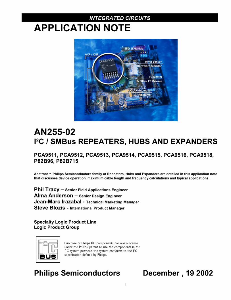
PCA9511, PCA9512, PP82B96, P82B715
Abstract - Philips Semiconductothat discusses device operation,
Phil Tracy – Senior Field
Alma Anderson – Seni
Jean-Marc Irazabal - TSteve Blozis - Internatio
Specialty Logic Product Logic Product Group
Philips Semico
INTEGRATED CIRCUITS
1
N NOTE
PEATERS, HUBS AND EXPANDERS
CA9513, PCA9514, PCA9515, PCA9516, PCA9518,
rs family of Repeaters, Hubs and Expanders are detailed in this application note maximum cable length and frequency calculations and typical applications.
Applications Engineer
or Design Engineer
echnical Marketing Manager
nal Product Manager
Line
nductors December , 19 2002
2
TABLE OF CONTENTS
TABLE OF CONTENTS ...................................................................................................................................................2OVERVIEW........................................................................................................................................................................3
DESCRIPTION .....................................................................................................................................................................3APPLICATIONS ...................................................................................................................................................................4DEVICE FEATURES AND CHARACTERISTICS.......................................................................................................................5DEVICE PINOUT .................................................................................................................................................................7ORDERING INFORMATION ..................................................................................................................................................7DATA SHEETS AND IBIS MODELS .....................................................................................................................................7
PCA9511/12/13/14 TECHNICAL INFORMATION .......................................................................................................7BLOCK DIAGRAM ..............................................................................................................................................................7
PCA9515/16/18 TECHNICAL INFORMATION ............................................................................................................9BLOCK DIAGRAM ..............................................................................................................................................................9VOLTAGE LEVEL TECHNICAL INFORMATION.....................................................................................................................9DESIGN CONSTRAINTS.....................................................................................................................................................10
P82B715 TECHNICAL INFORMATION......................................................................................................................11BLOCK DIAGRAM ............................................................................................................................................................11VOLTAGE LEVEL TECHNICAL INFORMATION...................................................................................................................11DESIGN CONSTRAINTS.....................................................................................................................................................12
P82B96 TECHNICAL INFORMATION........................................................................................................................13BLOCK DIAGRAM ............................................................................................................................................................13VOLTAGE LEVEL TECHNICAL INFORMATION...................................................................................................................14DESIGN CONSTRAINTS.....................................................................................................................................................14
USE OF MULTIPLE DEVICES IN THE SAME I2C SYSTEM..................................................................................15DETERMING PULL-UP RESISTORS VALUE...........................................................................................................16APPLICATIONS ..............................................................................................................................................................16
BUS EXPANSION BEYOND THE 400 PF LIMITATION .........................................................................................................16SPLIT BUS 100 KHZ AND 400 KHZ APPLICATION ............................................................................................................17VOLTAGE LEVEL SHIFTING..............................................................................................................................................17I2C MULTIPLEXING..........................................................................................................................................................18I2C MULTI-POINT HOT SWAP APPLICATIONS ..................................................................................................................19I2C BUS EXTENSION OVER LONG CABLES.......................................................................................................................19I2C OPTO-ELECTRICAL ISOLATION ..................................................................................................................................21MULTIPLE SEGMENT APPLICATION .................................................................................................................................22
FREQUENTLY ASKED QUESTIONS..........................................................................................................................23DEVICE USAGE AND DIFFERENCES ...................................................................................................................................23LIVE INSERTION ...............................................................................................................................................................25I2C OVER LONG DISTANCES .............................................................................................................................................27ELECTRICAL PARAMETERS...............................................................................................................................................30I2C PROTOCOL .................................................................................................................................................................35ARCHITECTURE / APPLICATIONS......................................................................................................................................36
ADDITIONAL INFORMATION....................................................................................................................................46APPENDIX 1 – Long Bus Calculations ..........................................................................................................................47
CALCULATION OF MAXIMUM CLOCK FREQUENCY FOR LONG BUSES ................................................................................47THE ‘SHORTCUT’ APPROACH TO LONG BUS APPLICATIONS...............................................................................................49SOME CALCULATION EXAMPLES ......................................................................................................................................50
APPENDIX 2 – Using P82B715 to increase the total allowable bus capacitance ........................................................52APPENDIX 3 - Operating P82B715 on lower supply voltages .....................................................................................53APPENDIX 4 - The special logic levels and noise margins of buffer logic ..................................................................54APPENDIX 5 - Using P82B96 to create a multi-drop “distribution” bus using 12 V logic levels..............................55APPENDIX 6 - Differences Between the LTC1694 and LTC1694-1............................................................................57APPENDIX 7 - Typical response times to 'data valid' on SDA, measured from the falling edge of SCL.................58
3
OVERVIEW
Description
The PCA9511, PCA9512, PCA9513, PCA9514, PCA9515, PCA9516, PCA9518, P82B715 and P82B96 allow a largeror longer I2C or SMBus system where the following constraints previously restricted its size:a) More I2C devices or larger wiring capacitance than the 400 pF maximum allowed in the I2C specification.b) Long bus wiring or backplanesc) Different operating supply voltages or logic voltage levels within one systemd) Opto-isolation for safety or due to difference in ground planee) Isolating a section of a system that has lost its power supplyf) Insertion of unpowered cards into an active I2C bus
With only one repeater delay between any two segments, the:- PCA9511/12/13/14 Hot Swappable I2C Buffers supports two segments of 400 pF and hot swapping with pin
precharge and idle detect features.- PCA9515 I2C Bus Repeater supports two segments of 400 pF with channel enable.- PCA9516 5-channel I2C Hub supports five segments of 400 pF for a total I2C or SMBus capacitance of 2000 pF
with 4 channel enables.- PCA9518 Expandable 5-channel I2C Hub supports multiple groupings of five segments of 400 pF each for an
unlimited I2C or SMBus capacitance with 4 channel enables per device.
The PCA9511/12/13/14 are designed to work with clock frequencies up to 400 kHz and are suitable for utilization in amulti-master I2C bus or SMBus environment. They are specifically designed for backplane multi-point applications andhot swap. The devices support bus arbitration and contention with bus masters located on any segment. They are multi-directional and require no direction control. Operational voltage supply is 2.7 V to 5.5 V with 5.5 V tolerant I/Os.Operational temperature range is -40 ºC to 85 ºC. See Philips application note AN10160-01 for more detailed technicalinformation on these devices.
The PCA9515/16/18 are designed to work with clock frequencies up to 400 kHz and are suitable for utilization in amulti-master I2C bus or SMBus environment. They are specifically designed for larger buses on single card applicationswith the PCA9516 or PCA9518 for star configuration point to point connections. The devices support bus arbitration andcontention with bus masters located on any segment. They are multi-directional and require no direction control.Operational voltage supply is 3.0 V to 3.6 V with I/Os that are 6.0 V tolerant allowing easy interfacing of 3.3 V and 5 Vdevices. Operational temperature range is -40 ºC to 85 ºC.
The P82B715 allows bi-directional signaling without an external direction control over wiring capacitance loads up toaround 3000 pF. At normal I2C logic voltage levels, it transforms the impedance of the wiring by a factor 10, so 3000 pFof wiring appears as 300 pF loading on the I2C bus. The P82B715 does not afford any isolation or support logic voltagelevel translation. The P82B96 is recommended for new designs due to its superior features.
The P82B96 allows bi-directional signaling without an external direction control and provides a true buffer functionalitysupporting logic levels from 2 V to 15 V and bus impedance 10 times lower than I2C. It is designed for long distancesignaling, multi-point applications and opto-isolation of bus segments in situations like power supplies with differentground planes.
Normally, only one PCA9515 Repeater or PCA9516 Hub should be used per I2C or SMBus system due to the way theyoperate to provide multi-directional signally without an external direction control. The PCA951x series of HotSwappable Bus Buffers, the PCA9518 Expandable Hub or the P82B715/96 Bus Buffers should be used for anyapplication requiring multiple devices in the same system.
This Application Note covers the use of these devices in a generic multiple master environment.. Information on thepermitted interfaces and bus propagation delays between P82B715/96 Buffers and PCA951x/15/16/18 are also included.
4
Applications
These devices can be used for a wide variety of applications:
I2C or SMBus Extension – All devices allow extension of the I2C or SMBus on systems requiring capacitance loadslarger than the 400 pF max specified by the I2C protocol. Designers can extend the use of the I2C or SMBus in systemswith more devices and / or longer bus lengths with only one repeater delay between any device. The devices are multiplemaster capable and support arbitration and bus contention on any segment.- The PCA9511/12/13/14/15 I2C Bus Repeater supports two I2C or SMBus branches of 400 pF- The PCA9516 5-channel I2C Hub enables separation of the I2C or SMBus into five 400 pF segments- The PCA9518 Expandable 5-channel I2C Hub enables separation of the I2C or SMBus into multiple groupings of
five 400-pF segments for star configurations.- The P82B715 and P82B96 provide the multi-point bus alternative. Working in the conventional I2C ‘wired and’
mode, but with an impedance level that may be 10 times lower than I2C thus allowing up to 4000 pF buscapacitance. P82B96 allows selection of any convenient logic voltage level up to 15 V with no restriction on thenumber of ‘drops’.
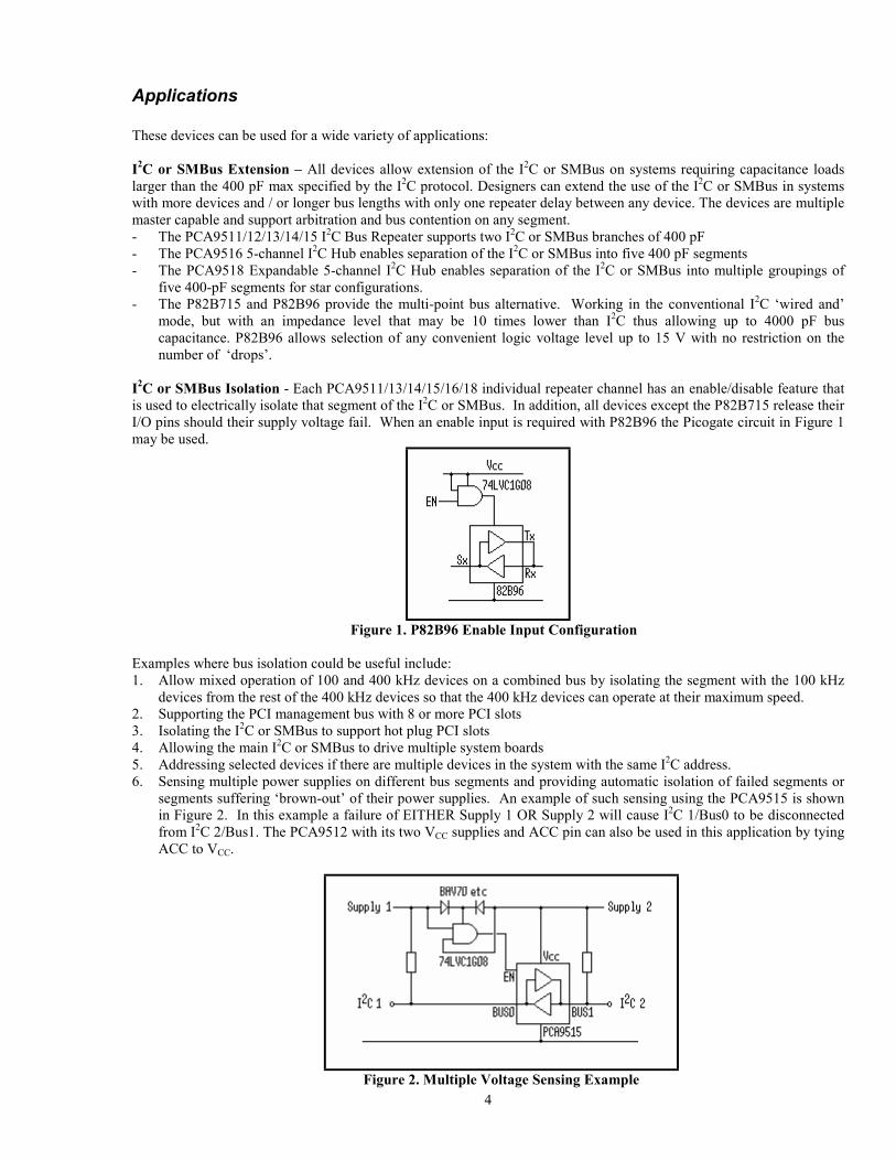
I2C or SMBus Isolation - Each PCA9511/13/14/15/16/18 individual repeater channel has an enable/disable feature thatis used to electrically isolate that segment of the I2C or SMBus. In addition, all devices except the P82B715 release theirI/O pins should their supply voltage fail. When an enable input is required with P82B96 the Picogate circuit in Figure 1may be used.
Figure 1. P82B96 Enable Input Configuration
Examples where bus isolation could be useful include:1. Allow mixed operation of 100 and 400 kHz devices on a combined bus by isolating the segment with the 100 kHz
devices from the rest of the 400 kHz devices so that the 400 kHz devices can operate at their maximum speed.2. Supporting the PCI management bus with 8 or more PCI slots3. Isolating the I2C or SMBus to support hot plug PCI slots4. Allowing the main I2C or SMBus to drive multiple system boards5. Addressing selected devices if there are multiple devices in the system with the same I2C address.6. Sensing multiple power supplies on different bus segments and providing automatic isolation of failed segments or
segments suffering ‘brown-out’ of their power supplies. An example of such sensing using the PCA9515 is shownin Figure 2. In this example a failure of EITHER Supply 1 OR Supply 2 will cause I2C 1/Bus0 to be disconnectedfrom I2C 2/Bus1. The PCA9512 with its two VCC supplies and ACC pin can also be used in this application by tyingACC to VCC.
Figure 2. Multiple Voltage Sensing Example
5
Voltage Translation - The PCA9515/16/18 operate on 3.3 V VCC but since they have 6.0 V tolerant I/Os, they supportdifferent I2C or SMBus segments at 3.3 V or 5 V, thus extending the life of older 5 V circuit blocks while allowing useof newer 3.3 V devices for improved system performance.
PCA9511/13/14 do NOT support logic level translations. The PCA9512 has two VCC supply inputs specificallydesigned for voltage translation applications.
P82B715 does NOT support logic level translations. Its I/O pins simply track each other within 100mV, independent ofthe power supply (VCC). Its logic levels may not exceed VCC and will be diode clamped at VCC + Vdiode.
P82B96 is intended for operation with 5 V logic on its Sx side but can operate down to 3.3 V. The logic threshold on theSx side is independent of the device’s VCC. The logic levels on the higher drive Rx/Tx side are half-rail CMOS switchinglevels related to the device’s supply (VCC) that is specified from 2 V to 15 V. All I/Os are 18 V tolerant.
The GTL2000/02/10 allow I2C voltage level translation at any voltage between 1.0 V and 5.0 V. See application noteAN10145-01 Bi-Directional Voltage Translators for more information.
Hot Swapping Line Cards - The PCA9511/12 are featured with circuitry that precharges the SDA and SCL pins toprevent glitching data on an active I2C bus when the unpowered slave card is inserted into the backplane system. Theyalso feature an idle detect circuit that will not connect the active bus to the line card devices until the bus is idle. ThePCA9513/14 do not have the precharge feature since it is not needed or desired in some applications. The PCA9513 hasa 92 µA current source for PICMG applications.
Device Features and Characteristics
PCA9511/12/13/14:• Bi-directional buffer for SDA and SCL lines• Prevents SDA and SCL corruption during live board insertion and removal from backplane
• Idle detect circuit connects board only when bus is idle• 1 V precharge on all SDA and SCL lines prevents data glitch (PCA9511/12 only)
• Compatible with I2C, I2C fast mode, and SMBus standards• DV/Dt rise time accelerators on all SDA and SCL lines• Rise time accelerator disable (PCA9512 only)• Low ICC device disable: <1 mA (PCA9511/13/14 only)• READY open-drain output (PCA9511/13/14 only)• 92 µA current source for PICMG applications (PCA9513 only)• Operating voltage range is 2.7 V to 5.5 V• 5.5 V tolerant I2C and enable pins• Split VCC for 3.3 V and 5 V level translation (PCA9512 only)• Operating temperature range is -40 ºC to 85 ºC• Accommodate 100 kHz and 400 kHz devices and multiple masters• ESD protection exceeds:
• 2000 V HBM per JESD22-A114• 200 V MM per JESD22-A115• 1000 V CDM per JESD22-C101
• Latch-up testing is done to JEDEC Standard JESD78 which exceeds 100 mA• PCA9511/12/13/14 offered in 8-pin SO (D) and TSSOP (DP)
PCA9515/16/18:• Accommodate more I2C devices or a longer bus length, up to 400 pF per segment• Multi-directional I2C drivers that require no directional control isolate the I2C bus capacitance of each segment.• Powered-off high impedance I2C pins support hot insertion and tolerant up to 6.0 V.• Open drain outputs and fail safe (will not inhibit attached devices) operation on loss of power• Designed for I2C-bus operation but compatible with SMBus• Lock-up free operation• Multi-master capable repeaters support bus arbitration and clock stretching with only one repeater delay betweensegments
6
• Operating voltage range is 3.0 V to 3.6 V• 6.0 V tolerant I2C and enable pins - pull-up resistors to either 3.3 V or 5 V voltage levels are allowed on the individualsegments since the I2C bus and enable pins are over voltage tolerant to 6.0 V.• Individual channel enables allow segments to be individually isolated. Hardware enable pins operate at LVTTL voltagelevels and are over voltage tolerant to 6.0 V.• Operating frequency range from 0 kHz to 400 kHz• Operating temperature range is -40 ºC to 85 ºC• ESD protection exceeds:
• 2000 V HBM per JESD22-A114• 200 V MM per JESD22-A115• 1000 V CDM per JESD22-C101
• Latch-up testing is done to JEDEC Standard JESD78 which exceeds 100 mA• PCA9515 offered in 8-pin SO (D) and TSSOP (DP)• PCA9516 offered in 16-pin SO narrow (D) and TSSOP (PW)• PCA9518 offered in 20-pin SO (D) and TSSOP (PW)
P82B715:• Accommodate more I2C devices or a longer, lower impedance bus wiring. Up to 3000 pF wiring capacitance.• Bi-directional unity voltage gain buffering with no external directional control required.• 10x impedance transformation but does not change logic voltage levels.• Wide supply voltage range of 3.0 V to 12.5 V.• Logic signal levels independent of device supply and may include (but not exceed) supply and ground.• I2C-bus compatible but not compatible with SMBus.• Manufactured in rugged bipolar process (includes diodes to VCC).• Operating frequency range from 0 kHz to 100 kHz• Operating temperature range is -40 ºC to 85 ºC• ESD protection exceeds:
• 2500 V HBM per Mil. Std. 883C – 3015.7• Latch-up free (bipolar process with no latching structures).• P82B715 offered in 8-pin DIP (N) and SO (D)
P82B96:• Can split bi-directional I2C signals into two unidirectional Tx and Rx data signals, or recombine these.• 10x bus impedance transformation option, unlimited bus drive capability with external transistor.• Multi-drop extension bus configuration supports full I2C protocol.• Open collector outputs and fail safe operation (will not inhibit attached devices) on loss of power.• Designed for I2C-bus operation and compatible with SMBus• Powered-off high impedance and 18 V rated I/O pins support hot insertion or cable plug-in.• Low supply current (1 mA)• Manufactured in rugged bipolar process.• Operating voltage range is 2.0 V to 15.0 V• 18 V tolerant I/O pins - pull-up resistors to different voltage levels are allowed on each side of the device.• Usual operating frequency range from 0 kHz to 400 kHz but will clock above 600 kHz• Operating temperature range is -40 ºC to 85 ºC• ESD protection exceeds:
• 3500 V HBM per JESD22-A114• 1000 V CDM per JESD22-C101
• Latch-up free (bipolar process with no latching structures).• P82B96 offered in 8-pin DIP (N), SO (D) and TSSOP (DP)
7
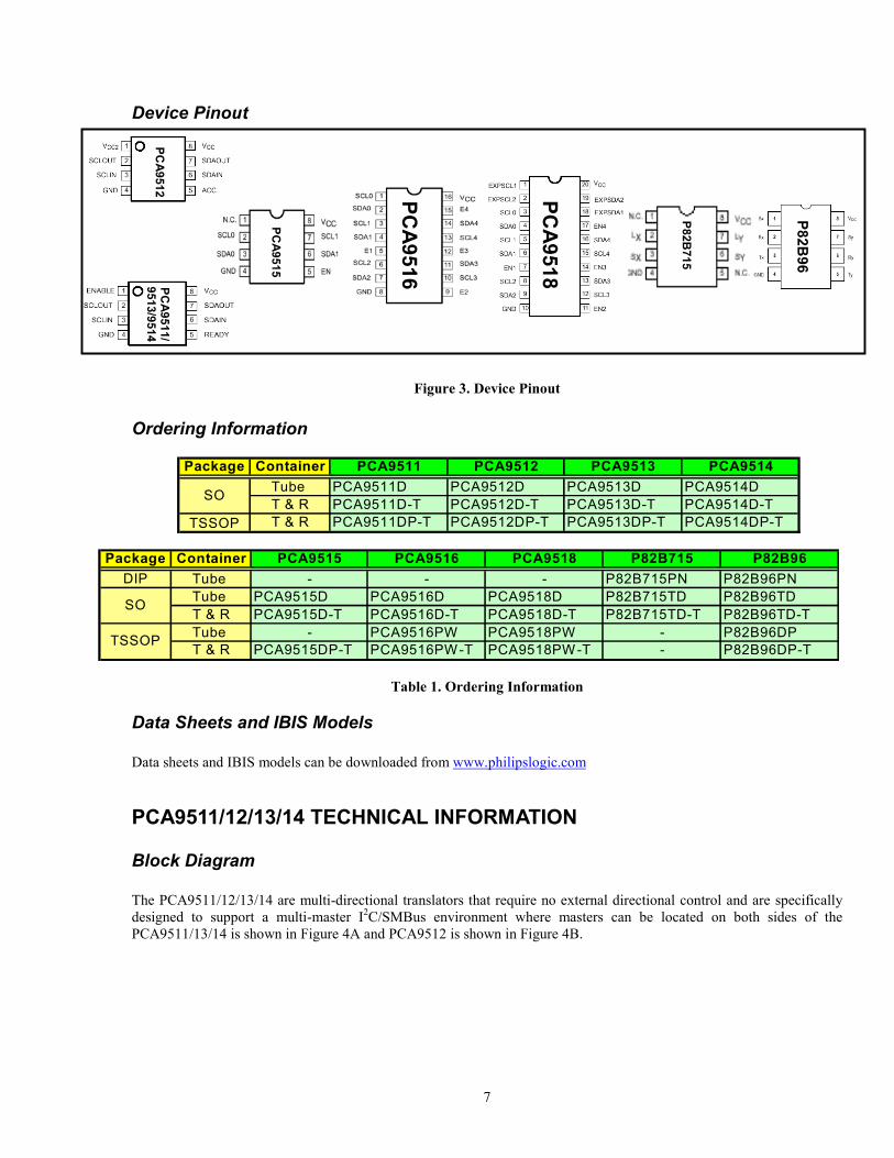
Device Pinout
Figure 3. Device Pinout
Ordering Information
Table 1. Ordering Information
Data Sheets and IBIS Models
Data sheets and IBIS models can be downloaded from www.philipslogic.com
PCA9511/12/13/14 TECHNICAL INFORMATION
Block Diagram
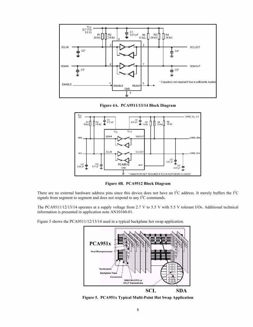
The PCA9511/12/13/14 are multi-directional translators that require no external directional control and are specificallydesigned to support a multi-master I2C/SMBus environment where masters can be located on both sides of thePCA9511/13/14 is shown in Figure 4A and PCA9512 is shown in Figure 4B.
Package Container PCA9511 PCA9512 PCA9513 PCA9514
Tube PCA9511D PCA9512D PCA9513D PCA9514DT & R PCA9511D-T PCA9512D-T PCA9513D-T PCA9514D-T
TSSOP T & R PCA9511DP-T PCA9512DP-T PCA9513DP-T PCA9514DP-T
SO
Package Container PCA9515 PCA9516 PCA9518 P82B715 P82B96
DIP Tube - - - P82B715PN P82B96PNTube PCA9515D PCA9516D PCA9518D P82B715TD P82B96TDT & R PCA9515D-T PCA9516D-T PCA9518D-T P82B715TD-T P82B96TD-TTube - PCA9516PW PCA9518PW - P82B96DPT & R PCA9515DP-T PCA9516PW-T PCA9518PW-T - P82B96DP-T
TSSOP
SO
PC
A9511/
9513/9514
PC
A9515
PC
A9516
P82B
715
P82B
96
PC
A9518
PC
A9512
8
Figure 4A. PCA9511/13/14 Block Diagram
Figure 4B. PCA9512 Block Diagram
There are no external hardware address pins since this device does not have an I2C address. It merely buffers the I2Csignals from segment to segment and does not respond to any I2C commands.
The PCA9511/12/13/14 operates at a supply voltage from 2.7 V to 5.5 V with 5.5 V tolerant I/Os. Additional technicalinformation is presented in application note AN10160-01.
Figure 5 shows the PCA9511/12/13/14 used in a typical backplane hot swap application.
Figure 5. PCA951x Typical Multi-Point Hot Swap Application
PCA951x
SCL SDA
9
PCA9515/16/18 TECHNICAL INFORMATION
Block Diagram
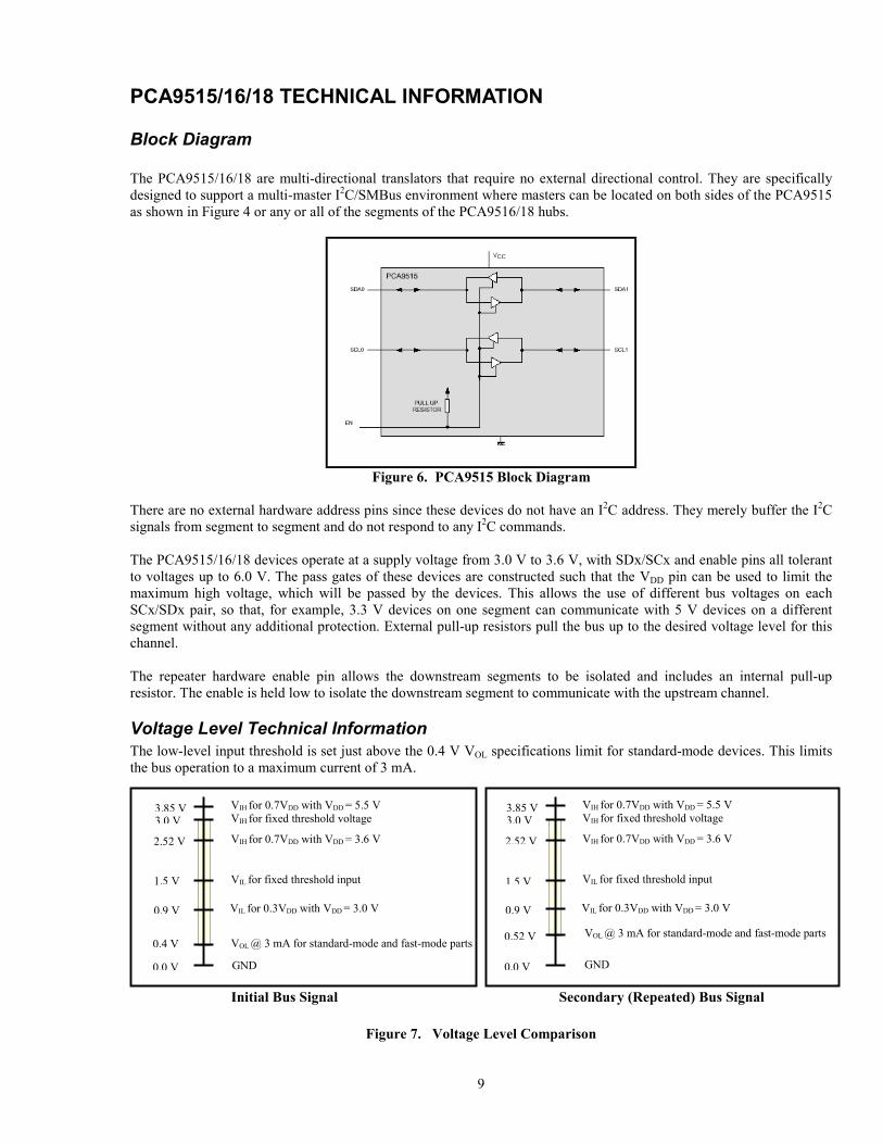
The PCA9515/16/18 are multi-directional translators that require no external directional control. They are specificallydesigned to support a multi-master I2C/SMBus environment where masters can be located on both sides of the PCA9515as shown in Figure 4 or any or all of the segments of the PCA9516/18 hubs.
Figure 6. PCA9515 Block Diagram
There are no external hardware address pins since these devices do not have an I2C address. They merely buffer the I2Csignals from segment to segment and do not respond to any I2C commands.
The PCA9515/16/18 devices operate at a supply voltage from 3.0 V to 3.6 V, with SDx/SCx and enable pins all tolerantto voltages up to 6.0 V. The pass gates of these devices are constructed such that the VDD pin can be used to limit themaximum high voltage, which will be passed by the devices. This allows the use of different bus voltages on eachSCx/SDx pair, so that, for example, 3.3 V devices on one segment can communicate with 5 V devices on a differentsegment without any additional protection. External pull-up resistors pull the bus up to the desired voltage level for thischannel.
The repeater hardware enable pin allows the downstream segments to be isolated and includes an internal pull-upresistor. The enable is held low to isolate the downstream segment to communicate with the upstream channel.
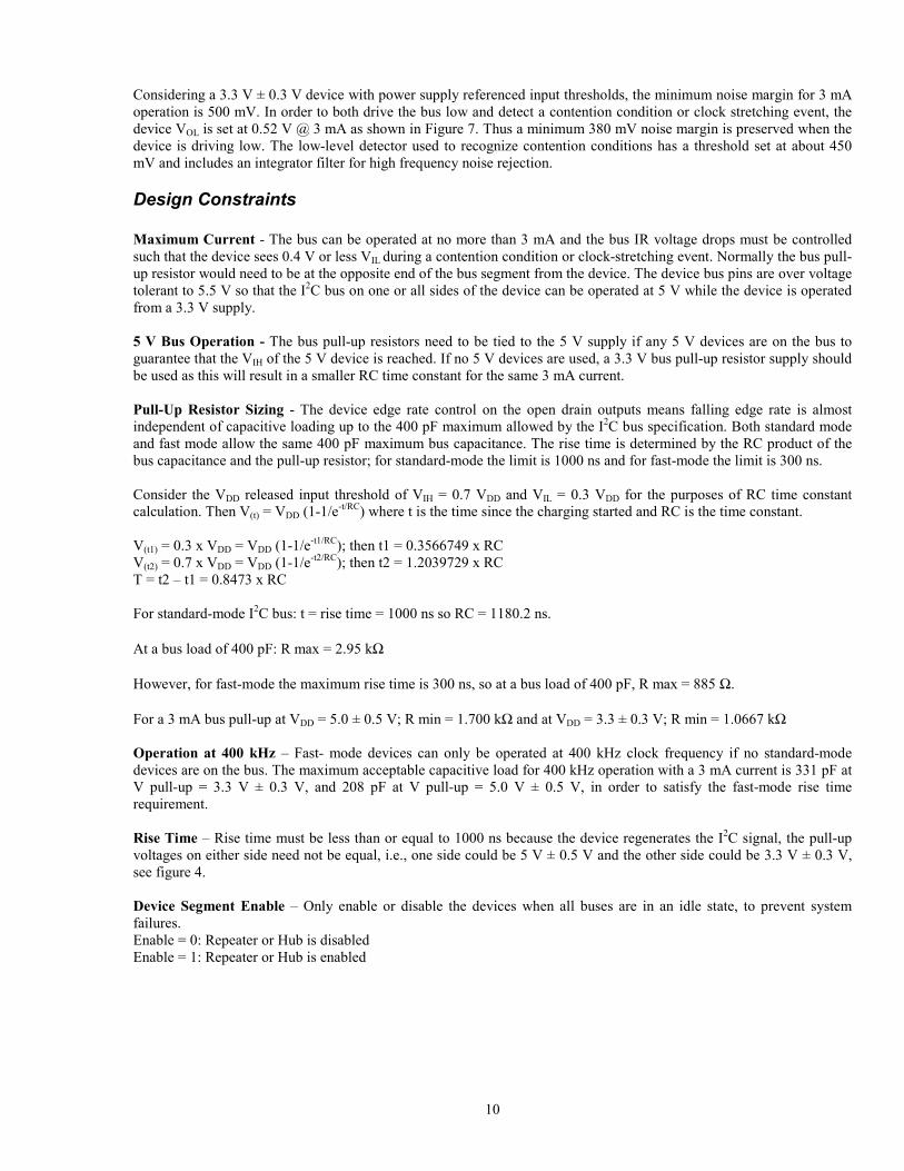
Voltage Level Technical InformationThe low-level input threshold is set just above the 0.4 V VOL specifications limit for standard-mode devices. This limitsthe bus operation to a maximum current of 3 mA.
Figure 7. Voltage Level Comparison
GND
VIH for 0.7VDD with VDD = 5.5 VVIH for fixed threshold voltage
VIH for 0.7VDD with VDD = 3.6 V
VIL for fixed threshold input
VIL for 0.3VDD with VDD = 3.0 V
VOL @ 3 mA for standard-mode and fast-mode parts
3.85 V3.0 V
2.52 V
1.5 V
0.9 V
0.4 V
0.0 V
VIH for 0.7VDD with VDD = 5.5 VVIH for fixed threshold voltage
VIH for 0.7VDD with VDD = 3.6 V
VIL for fixed threshold input
VIL for 0.3VDD with VDD = 3.0 V
VOL @ 3 mA for standard-mode and fast-mode parts
3.85 V3.0 V
2.52 V
1.5 V
0.9 V
0.52 V
0.0 V GND
Initial Bus Signal Secondary (Repeated) Bus Signal
10
Considering a 3.3 V ± 0.3 V device with power supply referenced input thresholds, the minimum noise margin for 3 mAoperation is 500 mV. In order to both drive the bus low and detect a contention condition or clock stretching event, thedevice VOL is set at 0.52 V @ 3 mA as shown in Figure 7. Thus a minimum 380 mV noise margin is preserved when thedevice is driving low. The low-level detector used to recognize contention conditions has a threshold set at about 450mV and includes an integrator filter for high frequency noise rejection.
Design Constraints
Maximum Current - The bus can be operated at no more than 3 mA and the bus IR voltage drops must be controlledsuch that the device sees 0.4 V or less VIL during a contention condition or clock-stretching event. Normally the bus pull-up resistor would need to be at the opposite end of the bus segment from the device. The device bus pins are over voltagetolerant to 5.5 V so that the I2C bus on one or all sides of the device can be operated at 5 V while the device is operatedfrom a 3.3 V supply.
5 V Bus Operation - The bus pull-up resistors need to be tied to the 5 V supply if any 5 V devices are on the bus toguarantee that the VIH of the 5 V device is reached. If no 5 V devices are used, a 3.3 V bus pull-up resistor supply shouldbe used as this will result in a smaller RC time constant for the same 3 mA current.
Pull-Up Resistor Sizing - The device edge rate control on the open drain outputs means falling edge rate is almostindependent of capacitive loading up to the 400 pF maximum allowed by the I2C bus specification. Both standard modeand fast mode allow the same 400 pF maximum bus capacitance. The rise time is determined by the RC product of thebus capacitance and the pull-up resistor; for standard-mode the limit is 1000 ns and for fast-mode the limit is 300 ns.
Consider the VDD released input threshold of VIH = 0.7 VDD and VIL = 0.3 VDD for the purposes of RC time constantcalculation. Then V(t) = VDD (1-1/e-t/RC) where t is the time since the charging started and RC is the time constant.
V(t1) = 0.3 x VDD = VDD (1-1/e-t1/RC); then t1 = 0.3566749 x RCV(t2) = 0.7 x VDD = VDD (1-1/e-t2/RC); then t2 = 1.2039729 x RCT = t2 – t1 = 0.8473 x RC
For standard-mode I2C bus: t = rise time = 1000 ns so RC = 1180.2 ns.
At a bus load of 400 pF: R max = 2.95 kΩ
However, for fast-mode the maximum rise time is 300 ns, so at a bus load of 400 pF, R max = 885 Ω.
For a 3 mA bus pull-up at VDD = 5.0 ± 0.5 V; R min = 1.700 kΩ and at VDD = 3.3 ± 0.3 V; R min = 1.0667 kΩ
Operation at 400 kHz – Fast- mode devices can only be operated at 400 kHz clock frequency if no standard-modedevices are on the bus. The maximum acceptable capacitive load for 400 kHz operation with a 3 mA current is 331 pF atV pull-up = 3.3 V ± 0.3 V, and 208 pF at V pull-up = 5.0 V ± 0.5 V, in order to satisfy the fast-mode rise timerequirement.
Rise Time – Rise time must be less than or equal to 1000 ns because the device regenerates the I2C signal, the pull-upvoltages on either side need not be equal, i.e., one side could be 5 V ± 0.5 V and the other side could be 3.3 V ± 0.3 V,see figure 4.
Device Segment Enable – Only enable or disable the devices when all buses are in an idle state, to prevent systemfailures.Enable = 0: Repeater or Hub is disabledEnable = 1: Repeater or Hub is enabled
11
P82B715 TECHNICAL INFORMATION
Block Diagram
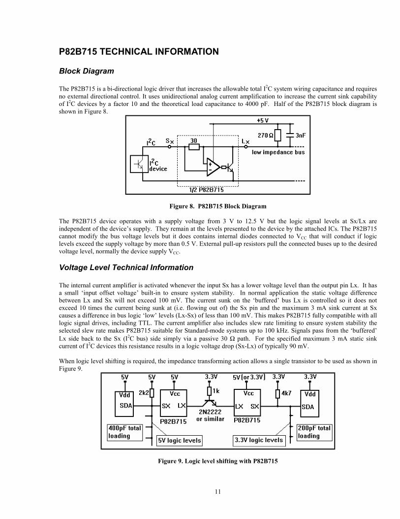
The P82B715 is a bi-directional logic driver that increases the allowable total I2C system wiring capacitance and requiresno external directional control. It uses unidirectional analog current amplification to increase the current sink capabilityof I2C devices by a factor 10 and the theoretical load capacitance to 4000 pF. Half of the P82B715 block diagram isshown in Figure 8.
Figure 8. P82B715 Block Diagram
The P82B715 device operates with a supply voltage from 3 V to 12.5 V but the logic signal levels at Sx/Lx areindependent of the device’s supply. They remain at the levels presented to the device by the attached ICs. The P82B715cannot modify the bus voltage levels but it does contains internal diodes connected to VCC that will conduct if logiclevels exceed the supply voltage by more than 0.5 V. External pull-up resistors pull the connected buses up to the desiredvoltage level, normally the device supply VCC.
Voltage Level Technical Information
The internal current amplifier is activated whenever the input Sx has a lower voltage level than the output pin Lx. It hasa small ‘input offset voltage’ built-in to ensure system stability. In normal application the static voltage differencebetween Lx and Sx will not exceed 100 mV. The current sunk on the ‘buffered’ bus Lx is controlled so it does notexceed 10 times the current being sunk at (i.e. flowing out of) the Sx pin and the maximum 3 mA sink current at Sxcauses a difference in bus logic ‘low’ levels (Lx-Sx) of less than 100 mV. This makes P82B715 fully compatible with alllogic signal drives, including TTL. The current amplifier also includes slew rate limiting to ensure system stability theselected slew rate makes P82B715 suitable for Standard-mode systems up to 100 kHz. Signals pass from the ‘buffered’Lx side back to the Sx (I2C bus) side simply via a passive 30 Ω path. For the specified maximum 3 mA static sinkcurrent of I2C devices this resistance results in a logic voltage drop (Sx-Lx) of typically 90 mV.
When logic level shifting is required, the impedance transforming action allows a single transistor to be used as shown inFigure 9.
Figure 9. Logic level shifting with P82B715
12
Design Constraints
5 V Bus Operation – The P82B715 was originally designed and specified for 5 V bus operation. The specification de-ratings that apply when its supply voltage is reduced below the data sheet value of 4.5 V are given in Appendix 3. Theabsolute minimum supply is 3 V.
Pull-Up Resistor Sizing - The pull-down current amplification provided by P82B715 allows reducing the pull-upresistors on its Lx bus side by a factor up to 10 times. Any capacitance connected on the Lx bus side is also “scaled” by afactor 1/10, so 1000 pF of loading at Lx only appears as 100 pF loading of the I2C bus at Sx whenever the buffer isactive. It is active whenever its Sx pin voltage is lower than its Lx pin voltage. While it is not mandatory to fit pull-upresistors on both sides of P82B715, it is usually best practice to do so. If no pull-up was fitted at Sx, and 200 pF wasconnected at Sx, then for a rising edge of Lx the amplification will be active and the charging current of the 200 pF willbe amplified by a factor 10. This means its ‘effective’ loading on the bus at Lx is 2000 pF! If a pull-up resistor was fittedat Sx, such that the natural rise-time of Sx becomes faster than the rise-time of the Lx side, then the amplifier inP82B715 will not be activated and there will be no slowing of the bus rise-time at Lx. In fact, there will be a tinyimprovement because any pull-up at Sx is always connected via 30 Ω to Lx.
A simple rule saves complex calculations:Use pull-ups on both sides of P82B715 and ensure that the rise-times calculated for each side meets the I2C requirementof 1 µs. This is met whenever their RC product is less than 1.18 µs (see paragraph “Pull-Up Resistor Sizing” page 10)
For the Lx side, all the normal I2C impedances may be reduced by a factor up to 10 because its static sink current is 30mA and the device provides a current gain of 10. The minimum pull-up resistor to 5 V ± 10% becomes (5.5 V - 0.4 V /30 mA) = 170 ohms. But that assumes this is the only pull-up in the system. That is allowed, but we recommend usingpull-ups on Sx as well. Because P82B715 does not isolate Lx from Sx, the ‘effective’ pull-up, referenced to any I2C bus(i.e., at Sx) must be calculated to ensure it does not exceed 3 mA.
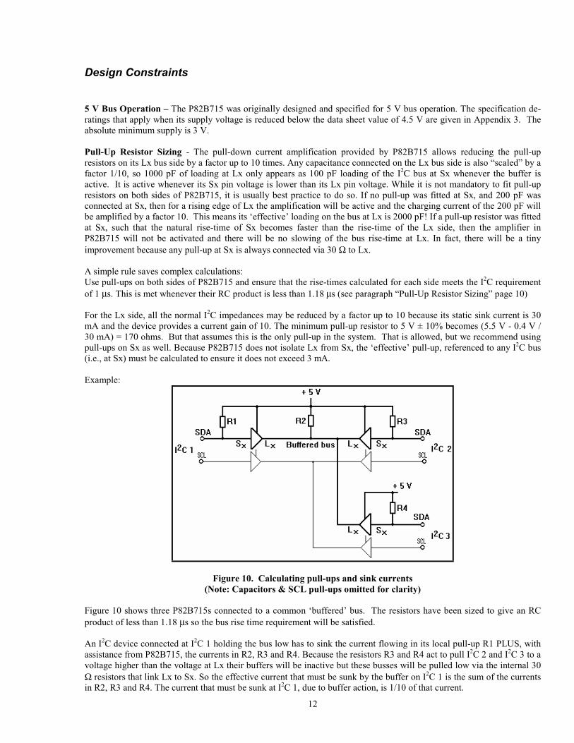
Example:
Figure 10. Calculating pull-ups and sink currents(Note: Capacitors & SCL pull-ups omitted for clarity)
Figure 10 shows three P82B715s connected to a common ‘buffered’ bus. The resistors have been sized to give an RCproduct of less than 1.18 µs so the bus rise time requirement will be satisfied.
An I2C device connected at I2C 1 holding the bus low has to sink the current flowing in its local pull-up R1 PLUS, withassistance from P82B715, the currents in R2, R3 and R4. Because the resistors R3 and R4 act to pull I2C 2 and I2C 3 to avoltage higher than the voltage at Lx their buffers will be inactive but these busses will be pulled low via the internal 30Ω resistors that link Lx to Sx. So the effective current that must be sunk by the buffer on I2C 1 is the sum of the currentsin R2, R3 and R4. The current that must be sunk at I2C 1, due to buffer action, is 1/10 of that current.
13
So the ‘effective’ pull-up, determining the current to be sunk by an I2C device at I2C 1 is R1 in parallel with resistors 10times the values of R2, R3 and R4. So, if R1 = R3 = R4 = 10 kΩ, and R2 = 1 kΩ , the pull-up load at I2C 1 is 10kΩ//10kΩ //100kΩ //100kΩ = 4.55 kΩ
The same calculation applies for I2C 2 and I2C 3.
To calculate the current being sunk by the Lx pin of the buffer at I2C 1, note that the current in R1 is being sunk directlyby the I2C device at I2C 1. The buffer therefore sinks the currents flowing in R2, R3, and R4. The effective pull-upequals R2//R3//R4. In this example, it is 1kΩ //10kΩ //10kΩ = 833 Ω. For a 5.5 V supply and 0.4 V low, that meansthe buffer is sinking 16.3 mA. Its rated static limit is 30 mA. So the requirement is that the pull-up on the buffered bus,in parallel with all other pull-ups at Sx pins that Lx is pulling low must be a net resistance greater than the allowedminimum of 170 Ω (for a 5 V system).
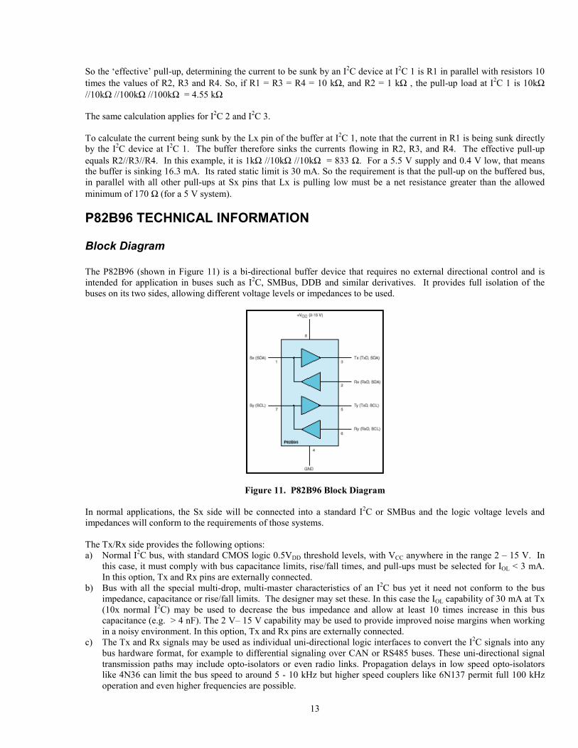
P82B96 TECHNICAL INFORMATION
Block Diagram
The P82B96 (shown in Figure 11) is a bi-directional buffer device that requires no external directional control and isintended for application in buses such as I2C, SMBus, DDB and similar derivatives. It provides full isolation of thebuses on its two sides, allowing different voltage levels or impedances to be used.
Figure 11. P82B96 Block Diagram
In normal applications, the Sx side will be connected into a standard I2C or SMBus and the logic voltage levels andimpedances will conform to the requirements of those systems.
The Tx/Rx side provides the following options:a) Normal I2C bus, with standard CMOS logic 0.5VDD threshold levels, with VCC anywhere in the range 2 – 15 V. In
this case, it must comply with bus capacitance limits, rise/fall times, and pull-ups must be selected for IOL < 3 mA.In this option, Tx and Rx pins are externally connected.
b) Bus with all the special multi-drop, multi-master characteristics of an I2C bus yet it need not conform to the busimpedance, capacitance or rise/fall limits. The designer may set these. In this case the IOL capability of 30 mA at Tx(10x normal I2C) may be used to decrease the bus impedance and allow at least 10 times increase in this buscapacitance (e.g. > 4 nF). The 2 V– 15 V capability may be used to provide improved noise margins when workingin a noisy environment. In this option, Tx and Rx pins are externally connected.
c) The Tx and Rx signals may be used as individual uni-directional logic interfaces to convert the I2C signals into anybus hardware format, for example to differential signaling over CAN or RS485 buses. These uni-directional signaltransmission paths may include opto-isolators or even radio links. Propagation delays in low speed opto-isolatorslike 4N36 can limit the bus speed to around 5 - 10 kHz but higher speed couplers like 6N137 permit full 100 kHzoperation and even higher frequencies are possible.
14
d) The Tx open collector output may be amplified (e.g. by adding a PNP transistor) to further increase the IOL to 300mA or more. This allows working over very long buses. See Appendix 1 for more details.
Voltage Level Technical Information
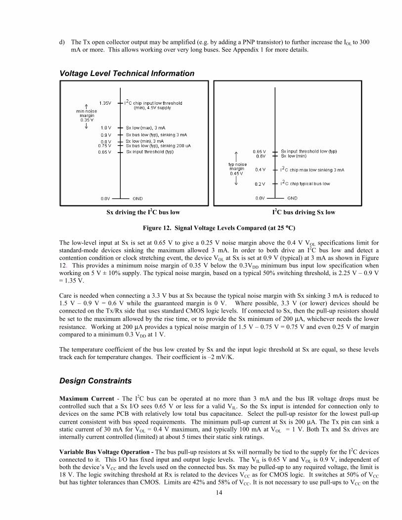
Sx driving the I2C bus low I2C bus driving Sx low
Figure 12. Signal Voltage Levels Compared (at 25 °°°°C)
The low-level input at Sx is set at 0.65 V to give a 0.25 V noise margin above the 0.4 V VOL specifications limit forstandard-mode devices sinking the maximum allowed 3 mA. In order to both drive an I2C bus low and detect acontention condition or clock stretching event, the device VOL at Sx is set at 0.9 V (typical) at 3 mA as shown in Figure12. This provides a minimum noise margin of 0.35 V below the 0.3VDD minimum bus input low specification whenworking on 5 V ± 10% supply. The typical noise margin, based on a typical 50% switching threshold, is 2.25 V – 0.9 V= 1.35 V.
Care is needed when connecting a 3.3 V bus at Sx because the typical noise margin with Sx sinking 3 mA is reduced to1.5 V – 0.9 V = 0.6 V while the guaranteed margin is 0 V. Where possible, 3.3 V (or lower) devices should beconnected on the Tx/Rx side that uses standard CMOS logic levels. If connected to Sx, then the pull-up resistors shouldbe set to the maximum allowed by the rise time, or to provide the Sx minimum of 200 µA, whichever needs the lowerresistance. Working at 200 µA provides a typical noise margin of 1.5 V – 0.75 V = 0.75 V and even 0.25 V of margincompared to a minimum 0.3 VDD at 1 V.
The temperature coefficient of the bus low created by Sx and the input logic threshold at Sx are equal, so these levelstrack each for temperature changes. Their coefficient is –2 mV/K.
Design Constraints
Maximum Current - The I2C bus can be operated at no more than 3 mA and the bus IR voltage drops must becontrolled such that a Sx I/O sees 0.65 V or less for a valid VIL. So the Sx input is intended for connection only todevices on the same PCB with relatively low total bus capacitance. Select the pull-up resistor for the lowest pull-upcurrent consistent with bus speed requirements. The minimum pull-up current at Sx is 200 µA. The Tx pin can sink astatic current of 30 mA for VOL = 0.4 V maximum, and typically 100 mA at VOL = 1 V. Both Tx and Sx drives areinternally current controlled (limited) at about 5 times their static sink ratings.
Variable Bus Voltage Operation - The bus pull-up resistors at Sx will normally be tied to the supply for the I2C devicesconnected to it. This I/O has fixed input and output logic levels. The VIL is 0.65 V and VOL is 0.9 V, independent ofboth the device’s VCC and the levels used on the connected bus. Sx may be pulled-up to any required voltage, the limit is18 V. The logic switching threshold at Rx is related to the devices VCC as for CMOS logic. It switches at 50% of VCC
but has tighter tolerances than CMOS. Limits are 42% and 58% of VCC. It is not necessary to use pull-ups to VCC on the
15
Tx/Rx interface provided it is recognized that VCC sets the logic threshold. So operating with VCC = 5 V sets the logicswitching level at 2.5 V but it is still allowed to connect to a bus operating with 12 V logic as long as the 1.25 V noisemargin (low) is acceptable.
Pull-Up Resistor Sizing – The calculations are the same as shown on paragraph “Pull-up Resistor Sizing” page 10 wheneither side of P82B96 is operated as a standard I2C bus. When the 10x drive capability is used then all resistances can bescaled down by a factor 10 and bus capacitance can be at least 10x greater.
Operation at 400 kHz – Although P82B96 will clock well above 600 kHz it was designed for operation up to 100 kHzbecause its propagation delays, and those of connected devices and long buses will rarely permit operation to 400 kHz.If timing calculations for a system indicate 400 kHz is within the necessary limits it can of course be used at the higherspeeds.
Rise Times – Bus rise and fall times, and capacitance limits, apply to any bus connected to I2C devices. When theTx/Rx side of P82B96 is being used at non-standard impedance or voltage levels (so only connected to other P82B96 orP82B715 devices) then no such limits apply and the designer is free to set these parameters to suit the application.
USE OF MULTIPLE DEVICES IN THE SAME I2C SYSTEM
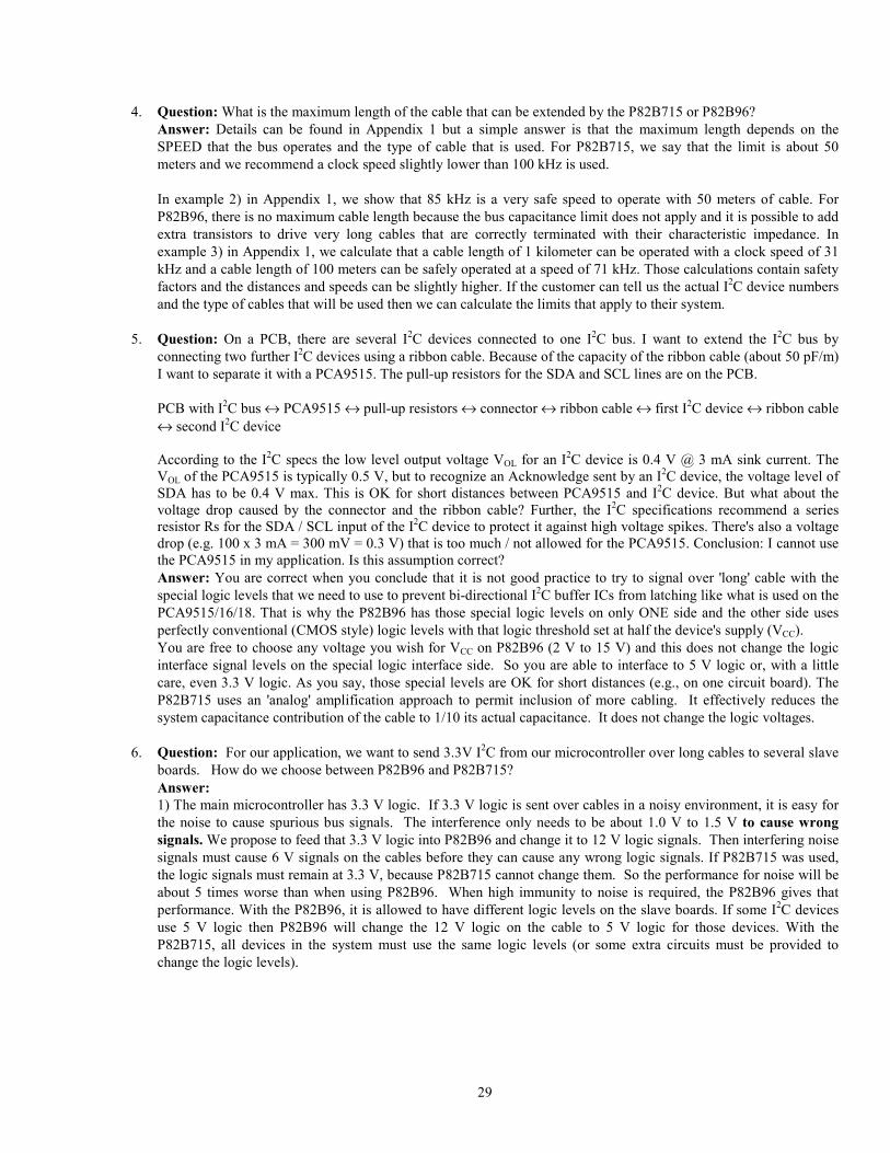
Series connection of PCA9515 and/or PCA9516 should not be attempted because the output of one device will not berecognized as a low for arbitration purposes by a second device. For the same reason, series connection between two SxI/O pins of the P82B96, or the interconnection of a Sx I/O of a P82B96 with a PCA9515 or PCA9516 is not permitted.Multiple PCA9511/12/13/14 Hot Swap Buffers can be used in series.
However, it is only the P82B96 Sx pins using special logic voltage levels that should not be interconnected. In thenormal application of both P82B96 and P82B715 it is intended that two devices will USUALLY be connected in series.The P82B715 uses normal I2C voltage levels, and only one side of P82B96 uses special levels. All sides of thePCA9515/16/18 use special levels.
There are no fundamental restrictions on making series connections between any of the following groups:A) The Tx/Rx side of P82B96B) Either side of the PCA9511/12/13/14C) Either side of P82B715D) Either side of just one PCA9515/16, OR just one Sx connection of a single P82B96
The selected system impedance levels, voltages, and propagation delays of course need to be considered.
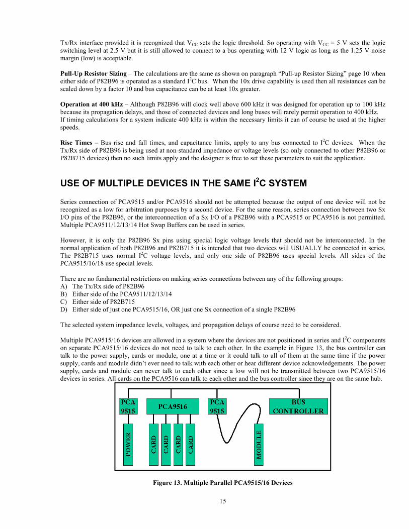
Multiple PCA9515/16 devices are allowed in a system where the devices are not positioned in series and I2C componentson separate PCA9515/16 devices do not need to talk to each other. In the example in Figure 13, the bus controller cantalk to the power supply, cards or module, one at a time or it could talk to all of them at the same time if the powersupply, cards and module didn’t ever need to talk with each other or hear different device acknowledgements. The powersupply, cards and module can never talk to each other since a low will not be transmitted between two PCA9515/16devices in series. All cards on the PCA9516 can talk to each other and the bus controller since they are on the same hub.
Figure 13. Multiple Parallel PCA9515/16 Devices
16
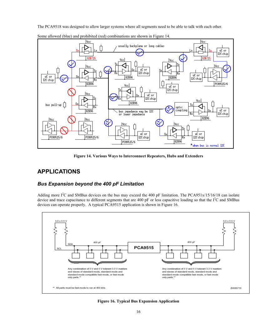
The PCA9518 was designed to allow larger systems where all segments need to be able to talk with each other.
Some allowed (blue) and prohibited (red) combinations are shown in Figure 14.
Figure 14. Various Ways to Interconnect Repeaters, Hubs and Extenders
APPLICATIONS
Bus Expansion beyond the 400 pF Limitation
Adding more I2C and SMBus devices on the bus may exceed the 400 pF limitation. The PCA951x/15/16/18 can isolatedevice and trace capacitance to different segments that are 400 pF or less capacitive loading so that the I2C and SMBusdevices can operate properly. A typical PCA9515 application is shown in Figure 16.
Figure 16. Typical Bus Expansion Application
17
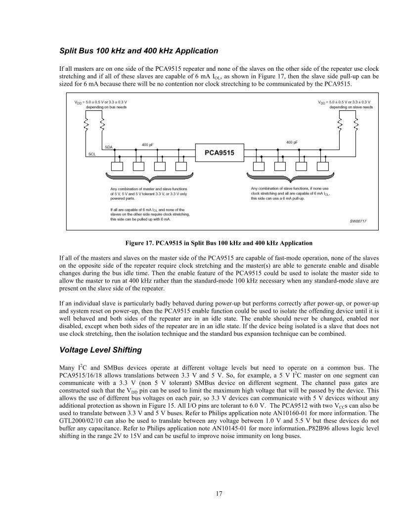
Split Bus 100 kHz and 400 kHz Application
If all masters are on one side of the PCA9515 repeater and none of the slaves on the other side of the repeater use clockstretching and if all of these slaves are capable of 6 mA IOL, as shown in Figure 17, then the slave side pull-up can besized for 6 mA because there will be no contention nor clock strectching to be communicated by the PCA9515.
Figure 17. PCA9515 in Split Bus 100 kHz and 400 kHz Application
If all of the masters and slaves on the master side of the PCA9515 are capable of fast-mode operation, none of the slaveson the opposite side of the repeater require clock stretching and the master(s) are able to generate enable and disablechanges during the bus idle time. Then the enable feature of the PCA9515 could be used to isolate the master side toallow the master to run at 400 kHz rather than the standard-mode 100 kHz necessary when any standard-mode slave arepresent on the slave side of the repeater.
If an individual slave is particularly badly behaved during power-up but performs correctly after power-up, or power-upand system reset on power-up, then the PCA9515 enable function could be used to isolate the offending device until it iswell behaved and both sides of the repeater are in an idle state. The enable should never be changed, enabled nordisabled, except when both sides of the repeater are in an idle state. If the device being isolated is a slave that does notuse clock stretching, then the isolation technique and the standard bus expansion technique can be combined.
Voltage Level Shifting
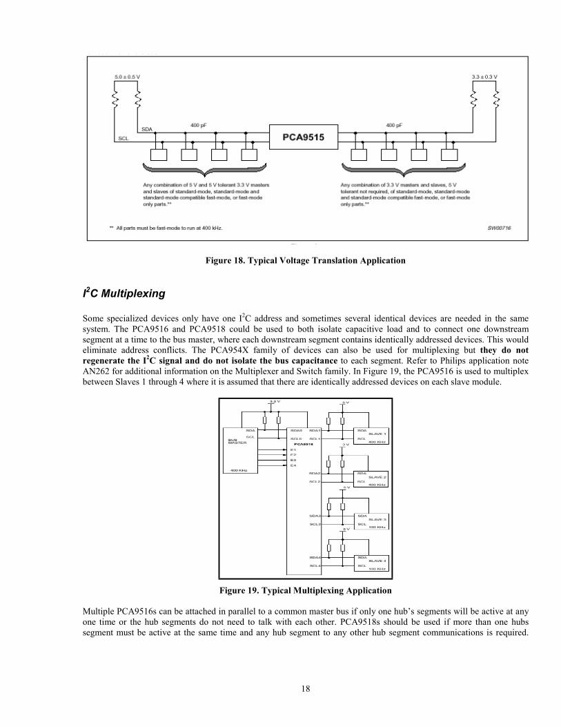
Many I2C and SMBus devices operate at different voltage levels but need to operate on a common bus. ThePCA9515/16/18 allows translations between 3.3 V and 5 V. So, for example, a 5 V I2C master on one segment cancommunicate with a 3.3 V (non 5 V tolerant) SMBus device on different segment. The channel pass gates areconstructed such that the VDD pin can be used to limit the maximum high voltage that will be passed by the device. Thisallows the use of different bus voltages on each pair, so 3.3 V devices can communicate with 5 V devices without anyadditional protection as shown in Figure 15. All I/O pins are tolerant to 6.0 V. The PCA9512 with two VCCs can also beused to translate between 3.3 V and 5 V buses. Refer to Philips application note AN10160-01 for more information. TheGTL2000/02/10 can also be used to translate between any voltage between 1.0 V and 5.5 V but these devices do notbuffer any capacitance. Refer to Philips application note AN10145-01 for more information..P82B96 allows logic levelshifting in the range 2V to 15V and can be useful to improve noise immunity on long buses.
18
Figure 18. Typical Voltage Translation Application
I2C Multiplexing
Some specialized devices only have one I2C address and sometimes several identical devices are needed in the samesystem. The PCA9516 and PCA9518 could be used to both isolate capacitive load and to connect one downstreamsegment at a time to the bus master, where each downstream segment contains identically addressed devices. This wouldeliminate address conflicts. The PCA954X family of devices can also be used for multiplexing but they do notregenerate the I2C signal and do not isolate the bus capacitance to each segment. Refer to Philips application noteAN262 for additional information on the Multiplexer and Switch family. In Figure 19, the PCA9516 is used to multiplexbetween Slaves 1 through 4 where it is assumed that there are identically addressed devices on each slave module.
Figure 19. Typical Multiplexing Application
Multiple PCA9516s can be attached in parallel to a common master bus if only one hub’s segments will be active at anyone time or the hub segments do not need to talk with each other. PCA9518s should be used if more than one hubssegment must be active at the same time and any hub segment to any other hub segment communications is required.
19
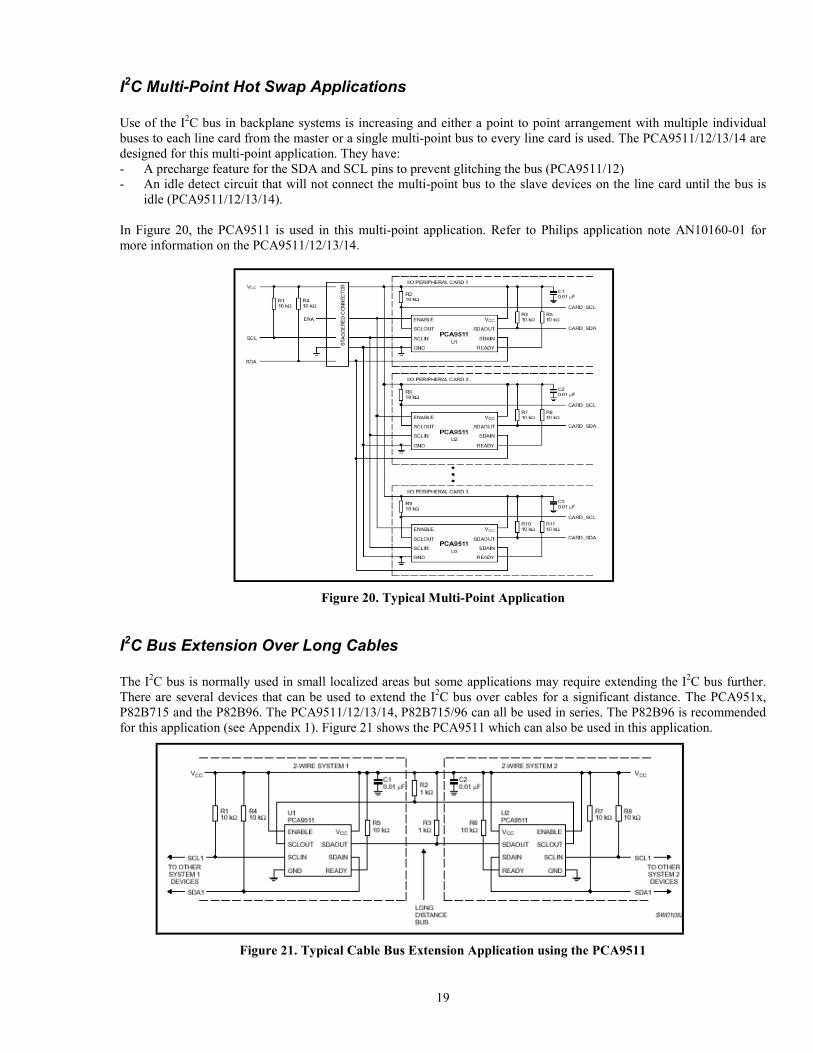
I2C Multi-Point Hot Swap Applications
Use of the I2C bus in backplane systems is increasing and either a point to point arrangement with multiple individualbuses to each line card from the master or a single multi-point bus to every line card is used. The PCA9511/12/13/14 aredesigned for this multi-point application. They have:- A precharge feature for the SDA and SCL pins to prevent glitching the bus (PCA9511/12)- An idle detect circuit that will not connect the multi-point bus to the slave devices on the line card until the bus is
idle (PCA9511/12/13/14).
In Figure 20, the PCA9511 is used in this multi-point application. Refer to Philips application note AN10160-01 formore information on the PCA9511/12/13/14.
Figure 20. Typical Multi-Point Application
I2C Bus Extension Over Long Cables
The I2C bus is normally used in small localized areas but some applications may require extending the I2C bus further.There are several devices that can be used to extend the I2C bus over cables for a significant distance. The PCA951x,P82B715 and the P82B96. The PCA9511/12/13/14, P82B715/96 can all be used in series. The P82B96 is recommendedfor this application (see Appendix 1). Figure 21 shows the PCA9511 which can also be used in this application.
Figure 21. Typical Cable Bus Extension Application using the PCA9511
20
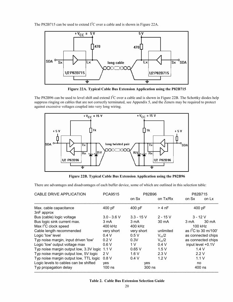
The P82B715 can be used to extend I2C over a cable and is shown in Figure 22A.
Figure 22A. Typical Cable Bus Extension Application using the P82B715
The P82B96 can be used to level shift and extend I2C over a cable and is shown in Figure 22B. The Schottky diodes helpsuppress ringing on cables that are not correctly terminated, see Appendix 5, and the Zeners may be required to protectagainst excessive voltages coupled into very long wiring.
Figure 22B. Typical Cable Bus Extension Application using the P82B96
There are advantages and disadvantages of each buffer device, some of which are outlined in this selection table:
CABLE DRIVE APPLICATION PCA9515 P82B96 P82B715on Sx on Tx/Rx on Sx on Lx
------------------------------------------------------------------------------------------------------------------------------------------------Max. cable capacitance 400 pF 400 pF > 4 nF 400 pF 3nF approxBus (cable) logic voltage 3.0 - 3.6 V 3.3 - 15 V 2 - 15 V 3 - 12 VBus logic sink current max. 3 mA 3 mA 30 mA 3 mA 30 mAMax I2C clock speed 400 kHz 400 kHz 100 kHzCable length recommended very short very short unlimited as I2C to 30 m/100'Logic 'low' level 0.4 V 0.5 V Vcc/2 as connected chipsTyp noise margin, input driven 'low' 0.2 V 0.3V Vcc/2 as connected chipsLogic 'low' output voltage max 0.6 V 1 V 0.4 V input level +0.1VTyp noise margin output low, 3.3V logic 1.1 V 0.65 V 1.5 V 1.4 VTyp noise margin output low, 5V logic 2 V 1.6 V 2.3 V 2.2 VTyp noise margin output low, TTL logic 0.8 V 0.4 V 1.2 V 1.1 VLogic levels to cables can be shifted yes yes noTyp propagation delay 100 ns 300 ns 400 ns------------------------------------------------------------------------------------------------------------------------------------------------
Table 2. Cable Bus Extension Selection Guide
21
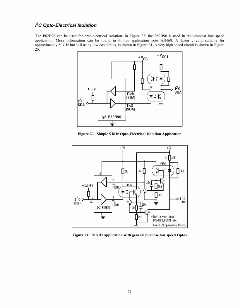
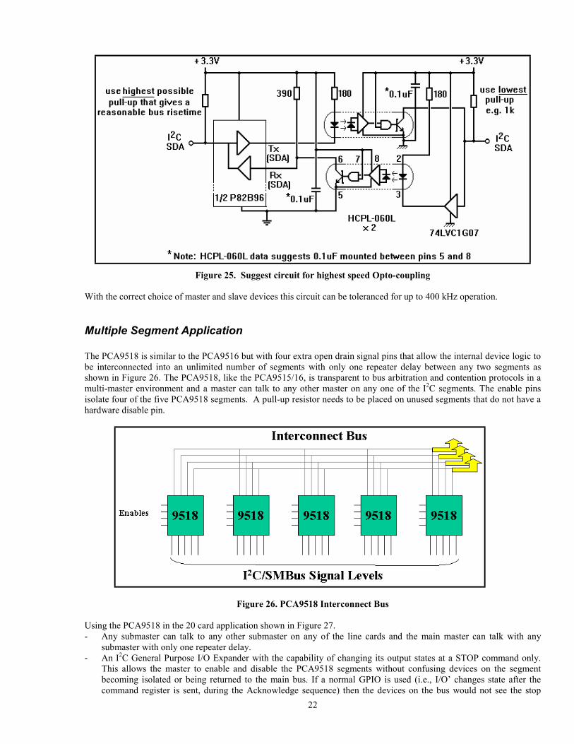
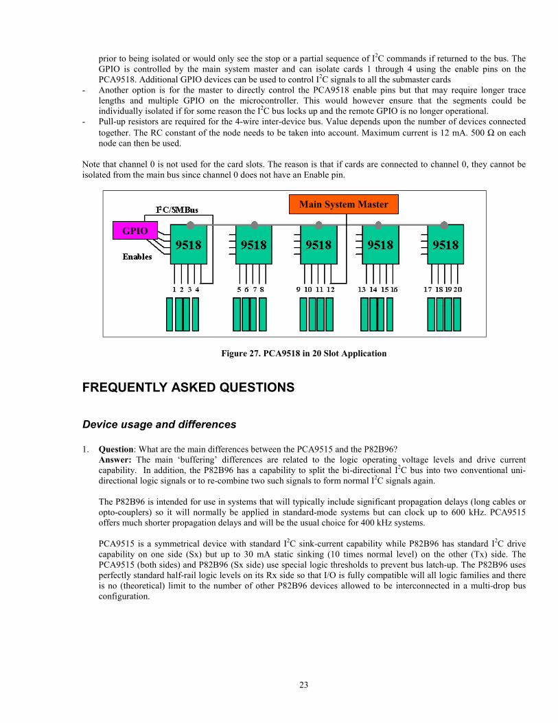
I2C Opto-Electrical Isolation
The P82B96 can be used for opto-electrical isolation. In Figure 23, the P82B96 is used in the simplest low speedapplication. More information can be found in Philips application note AN460. A faster circuit, suitable forapproximately 50kHz but still using low cost Optos, is shown in Figure 24. A very high speed circuit is shown in Figure25.
Figure 23. Simple 5 kHz Opto-Electrical Isolation Application
Figure 24. 50 kHz application with general purpose low speed Optos
22
Figure 25. Suggest circuit for highest speed Opto-coupling
With the correct choice of master and slave devices this circuit can be toleranced for up to 400 kHz operation.
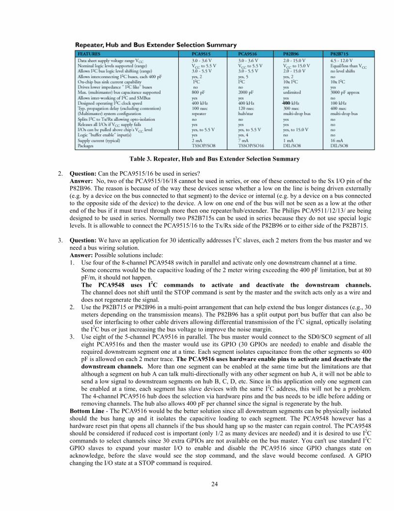
Multiple Segment Application
The PCA9518 is similar to the PCA9516 but with four extra open drain signal pins that allow the internal device logic tobe interconnected into an unlimited number of segments with only one repeater delay between any two segments asshown in Figure 26. The PCA9518, like the PCA9515/16, is transparent to bus arbitration and contention protocols in amulti-master environment and a master can talk to any other master on any one of the I2C segments. The enable pinsisolate four of the five PCA9518 segments. A pull-up resistor needs to be placed on unused segments that do not have ahardware disable pin.
Figure 26. PCA9518 Interconnect Bus
Using the PCA9518 in the 20 card application shown in Figure 27.- Any submaster can talk to any other submaster on any of the line cards and the main master can talk with any
submaster with only one repeater delay.- An I2C General Purpose I/O Expander with the capability of changing its output states at a STOP command only.
This allows the master to enable and disable the PCA9518 segments without confusing devices on the segmentbecoming isolated or being returned to the main bus. If a normal GPIO is used (i.e., I/O’ changes state after thecommand register is sent, during the Acknowledge sequence) then the devices on the bus would not see the stop
23
prior to being isolated or would only see the stop or a partial sequence of I2C commands if returned to the bus. TheGPIO is controlled by the main system master and can isolate cards 1 through 4 using the enable pins on thePCA9518. Additional GPIO devices can be used to control I2C signals to all the submaster cards
- Another option is for the master to directly control the PCA9518 enable pins but that may require longer tracelengths and multiple GPIO on the microcontroller. This would however ensure that the segments could beindividually isolated if for some reason the I2C bus locks up and the remote GPIO is no longer operational.
- Pull-up resistors are required for the 4-wire inter-device bus. Value depends upon the number of devices connectedtogether. The RC constant of the node needs to be taken into account. Maximum current is 12 mA. 500 Ω on eachnode can then be used.
Note that channel 0 is not used for the card slots. The reason is that if cards are connected to channel 0, they cannot beisolated from the main bus since channel 0 does not have an Enable pin.
Figure 27. PCA9518 in 20 Slot Application
FREQUENTLY ASKED QUESTIONS
Device usage and differences
1. Question: What are the main differences between the PCA9515 and the P82B96?Answer: The main ‘buffering’ differences are related to the logic operating voltage levels and drive currentcapability. In addition, the P82B96 has a capability to split the bi-directional I2C bus into two conventional uni-directional logic signals or to re-combine two such signals to form normal I2C signals again.
The P82B96 is intended for use in systems that will typically include significant propagation delays (long cables oropto-couplers) so it will normally be applied in standard-mode systems but can clock up to 600 kHz. PCA9515offers much shorter propagation delays and will be the usual choice for 400 kHz systems.
PCA9515 is a symmetrical device with standard I2C sink-current capability while P82B96 has standard I2C drivecapability on one side (Sx) but up to 30 mA static sinking (10 times normal level) on the other (Tx) side. ThePCA9515 (both sides) and P82B96 (Sx side) use special logic thresholds to prevent bus latch-up. The P82B96 usesperfectly standard half-rail logic levels on its Rx side so that I/O is fully compatible will all logic families and thereis no (theoretical) limit to the number of other P82B96 devices allowed to be interconnected in a multi-drop busconfiguration.
GPIO
Main System Master
24
Table 3. Repeater, Hub and Bus Extender Selection Su
2. Question: Can the PCA9515/16 be used in series?Answer: No, two of the PCA9515/16/18 cannot be used in series, or one of thesP82B96. The reason is because of the way these devices sense whether a low on(e.g. by a device on the bus connected to that segment) to the device or internal (to the opposite side of the device) to the device. A low on one end of the bus wend of the bus if it must travel through more then one repeater/hub/extender. Thedesigned to be used in series. Normally two P82B715s can be used in series belevels. It is allowable to connect the PCA9515/16 to the Tx/Rx side of the P82B9
3. Question: We have an application for 30 identically addresses I2C slaves, each 2need a bus wiring solution.Answer: Possible solutions include:1. Use four of the 8-channel PCA9548 switch in parallel and activate only one
Some concerns would be the capacitive loading of the 2 meter wiring exceedpF/m, it should not happen.The PCA9548 uses I2C commands to activate and deactivaThe channel does not shift until the STOP command is sent by the master andoes not regenerate the signal.
2. Use the P82B715 or P82B96 in a multi-point arrangement that can help extemeters depending on the transmission means). The P82B96 has a split outpused for interfacing to other cable drivers allowing differential transmission the I2C bus or just increasing the bus voltage to improve the noise margin.
3. Use eight of the 5-channel PCA9516 in parallel. The bus master would coneight PCA9516s and then the master would use its GPIO (30 GPIOs arerequired downstream segment one at a time. Each segment isolates capacitapF is allowed on each 2 meter trace. The PCA9516 uses hardware enable pdownstream channels. More than one segment can be enabled at the samalthough a segment on hub A can talk multi-directionally with any other segmsend a low signal to downstream segments on hub B, C, D, etc. Since in thibe enabled at a time, each segment has slave devices with the same I2C aThe 4-channel PCA9516 hub does the selection via hardware pins and the bremoving channels. The hub also allows 400 pF per channel since the signal
Bottom Line - The PCA9516 would be the better solution since all downstream should the bus hang up and it isolates the capacitive loading to each segmehardware reset pin that opens all channels if the bus should hang up so the masteshould be considered if reduced cost is important (only 1/2 as many devices are commands to select channels since 30 extra GPIOs are not available on the busGPIO slaves to expand your master I/O to enable and disable the PCA95acknowledge, before the slave would see the stop command, and the slave changing the I/O state at a STOP command is required.
400
mmary
e connected to the Sx I/O pin of the the line is being driven externally
e.g. by a device on a bus connectedill not be seen as a low at the other Philips PCA9511/12/13/ are beingcause they do not use special logic6 or to either side of the P82B715.
meters from the bus master and we
downstream channel at a time.ing the 400 pF limitation, but at 80
te the downstream channels.d the switch acts only as a wire and
nd the bus longer distances (e.g., 30ut port bus buffer that can also be
of the I2C signal, optically isolating
nect to the SD0/SC0 segment of all needed) to enable and disable thence from the other segments so 400ins to activate and deactivate thee time but the limitations are thatent on hub A, it will not be able to
s application only one segment canddress, this will not be a problem.us needs to be idle before adding oris regenerate by the hub.segments can be physically isolatednt. The PCA9548 however has ar can regain control. The PCA9548needed) and it is desired to use I2C master. You can't use standard I2C16 since GPIO changes state onwould become confused. A GPIO
25
4. Question: We are passing signals from a PCA9515 through the PCA9544. On the I2C bus lines, they are using a 1.3kΩ pull-up to 3.3 V on the PCA9515 side of the pass transistor and a 20 kΩ pull up to 3.3 V on the other. We see aPCA9515 Vol = 0.5 V to 0.6 V and on the other side of the pass transistor a signal level of 0.7 V to 0.8 V. Thismakes the combination unsuitable for use with a Linear Tech LTC4300-1 (which has a max Vil spec. of 0.6 Vand which is used on the other side of the pass transistor). Does Philips have a plot of Vol vs Iol for the PCA9515 -if we're at 0.6 V @ 2.7 mA, we will be out of data sheet specification at 6 mA. Using the 20 kΩ ohm resistors, theyappear to be limiting the amount of current through the pass transistor in order to reduce the drop across it. From thecalculations, they have about 165 µA of pull-up current through the pass transistor. To get a 200 mV delta Ron isquite considerable. Do we see any Ron dependency with through current?Answer: You are suffering from one of the unintended outcomes of using the LTC4300-1 device.- The PCA9515 uses an output driver that is essentially a voltage source that only sinks current and its level is set
at 0.52 V. Thus, from zero to more than 10 mA, the output voltage only changes by a few millivolts. Even withvariations over process, temperature, and power supply, the voltage is within a few tens of millivolts of 0.52 V.The output voltage at even 10 mA is less than 0.6 V.
- The maximum Ron for the PCA9544 is 55 Ω. Assuming 135 µA from the 20 kΩ resistor, the voltage dropacross the PCA9544 should be less than 0.01 V. Even at 55 Ω Ron, which is the maximum limit, to get a 0.2 Vdrop across the PCA9544 would require 3.6 mA.
Therefore, the LTC4300-1 is the most likely source of the extra current. I believe a check of the system with theLTC4300-1 removed will confirm that the voltage driven at the output of the PCA9544 is less than 0.6 V. Theproblem is that the "pull-up" current one-shot in the LTC4300-1 is being triggered by noise and is contending withthe low level driven by the PCA9515. The pull-up current source in the LTC4300-1 speeds the low to high transitionby increasing the total pull-up current and is switched off when the pin is high so as not to contend on the next highto low transition. If the current source of the LTC4300-1 gets turned on when the PCA9515 is driving a low, it willremain on because the pin does not go high. The current supplied by the current source will be high enough to pullthe voltage up to 0.7 V - 0.8 V.Note: The LTC4300-1 is 100% equivalent to the Philips PCA9511 and the LTC4300-2 is 100% equivalent to thePhilips PCA9512.
5. Question: We are having problems with the PCA9516 and want to replace it with an analog multiplexer solution.Can you share any information to justify the need for these hub devices and discuss in more detail how arbitration isused (beyond what is in the data sheet)?Answer: The PCA9515/16 provide the principal benefit of allowing the system to be increased in size well beyondthe 400 pF limit in the I2C specification by physically separating the system into branches. Each branch can beloaded up to 400 pF. The enables can be used to isolate faulty branches, or resolve address conflicts, however toprevent system problems the enable pins should only be switched during an idle state. Acknowledge and arbitrationis fundamental aspects of I2C protocol. Arbitration only applies to multiple master systems however acknowledge isused between master and slave to confirm byte transactions. If you only need to multiplex the lines and loading isnot a problem, we offer a family of I2C controlled multiplexers and switches under the PCA954X series.
Live insertion
1. Question: Can the PCA9515 be used in a Hot Insertion application? I’m worried about when the main systempower is off and the PCA9515 is not energized. What happens when one of the cards is plugged in? Could the activeI2C signal voltage damage the device?Answer: When the PCA9515/16/18 are powered off, the SCL and SDA pins are in a high impedance state so avoltage being applied to them will not damage the devices. The PCA9511/12/13/14 are specially designed for hotswap applications.
2. Question: Is it possible to pull up some of the hub downstream I2C channels to a permanent supply line and someothers to a switched supply lines?Answer: When the hub is in operation and the channel is enabled, the channel termination voltage must be on topull the I2C bus high. If the channel is disabled, then the channel termination voltage can be turned off.
26
3. Question: If the PCA9516 is powered up and a channel enabled what will happen if I remove the channel's pull-upvoltage?Answer: If the power supply is turned off, it will almost certainly pull low. If the power supply is removed, then theleakage current will determine what happens. If the leakage to ground dominates, it will go low and if the leakage toa high dominates it will stay high. (High is an unlikely outcome especially if no power is present).
4. Question: In the theory of operation you refer to a pull-down resistor - if I remove the pull-up voltage will I in factpull down to GND and lock every channel up?Answer: Most likely, if the channel is enabled and drifts low because the pull up supply is removed it is recognizedas a low and will be repeated on all enabled channels for as long as the condition exists or until the channel isdisabled, which ever comes first.
5. Question: What is the behavior of the PCA9516 hub when the switched supply is switched off?Answer: When power is cut to the PCA9516 hub, the device outputs go to a high impedance state and nocommunication through the hub is possible. When in a high impedance state, the outputs will not affect operation ofthe segment and normal I2C communications are possible on that segment, however, none of the 5 segments will beable to talk to each other. However care must be taken if segments are conducting independent conversations whenreconnecting or restoring power. Discussion of the software routines to cover all the possibilities during powerfailures or hot-plugging is beyond the scope of this application note and will be covered separately.
6. Question: Does the PCA9516 Hub power supply need to be put on the same supply that powers the microcontroller(permanent supply) or a switched supply?Answer: It does not matter to the PCA9516 hub. If it is the permanent power supply then the device is always activeand the downstream channel need to be pulled high or disabled. If switched off, all outputs go to a high impedancestate and no communication is possible through the hub.
7. Question: What about Fault Tolerance? How do the devices fail? Would it be possible to tri-state the I2C businterface in case there is a problem and makes the bus hanging up? This would make our system better and will givethem a better Fault Tolerance.Answer: Modern ICs have extremely low failure rates so failures will almost always be due to overstress.Overstress can be prevented by applying protection measures where the likelihood of overstress justifies this extracost. Devices like P82B96 have very high typical breakdown voltages, over 25 V on the Sx and almost 50 V on Txpins so it is relatively easy to apply protection clamps set at around the data sheet limit voltage (15 V – 18 V) thatwill not influence normal operation.
The P82B96 is relatively new and has no reported failures. It is closely related in technology to P82B715. In sellingthat device for 7 years I think the Quality and Failure Analysis lab has only ever seen about 4 defective productsreturned. All were at the same time and due to an unusual customer application that was not protected in our testingor data. We calculated the chance of other faulty devices at 1 in 10,000 and even that was restricted to production ina short time interval (due to a mask defect) it cannot happen again because we have added factory tests for it. I amnot aware of any field returns for any cause in the last 4 years (since that test was added), or in the earlier period.The PCA9511/12/13/14/15/16/18 and P82B96 are designed to release their I/Os if their power supply fails, so thebus is available for other devices to communicate. The PCA9515 Repeater and PCA9516/18 Hubs also features anEnable pin that provides the tri-state function. So several devices are offered that can be used to isolate failureproblems PROVIDED the problems can be software-diagnosed -- for example by isolating sections of the bus inturn and testing for shorts until the faulty section is found.
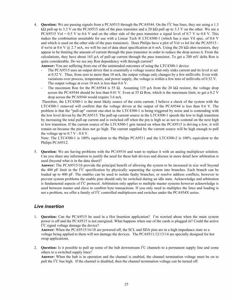
It is also possible to include simple hardware circuits that check the state of the bus lines and cause disconnection ofsections if the bus stays low for longer than a designed period. Some SMBus devices integrate this function. Anexample of such hardware is shown in Figure 28.
27
Figure 28. Bus “stuck low” sensor schematic
I2C over long distances
1. Question: The PCA9515 is being used in the network between the server and peripherals.- Is there any rule for the distance of I2C Bus?- Is there any method to improve signal quality in the I2C Bus in the cable length of 1m?Answer: There is no maximum length specified in the I2C specification. The limit of the length is a function ofseveral factors including capacitance (usual maximum limit is 400 pF), the minimum value for Rp, propagationdelays along the cables, the type of cable used and the integrity of the logic signals in the presence of noise. Thereare bus rise and fall times that must be met with limits set by the static and dynamic sink capability of standard I2Cdevices (3 mA sink current etc). There are some ways to improve the rise time by using a switched pull up circuit.At 400 kHz data rates, there is not any problem with transit time for just 1 meter of cabling. This assumes thequestion refers to cable propagation delay, then there’s no ‘problem’ with PCA9515 (100 ns each way) and noproblem with 1 meter (10 ns round trip) and a bus ‘low’ time of 1.3 µs. Appendix 1 covers these complexcalculations.
2. Question: There is an old P82B715 App note about a “mile long” I2C. Is that practical?Answer: No, certainly not for P82B715. In real applications it is fine (conservatively and well proven) to about 100feet at 5 V at 100 kHz. It was explained in the application note that the result was obtained only under perfect labconditions, and with low clock speeds. Signal propagation delays over a mile are around 17 microseconds meaningthe clock speed certainly cannot exceed about 25 kHz. If a mile is really needed then it could be achieved using theP82B96 with the circuit in Appendix 1 provided the necessary protection against things like lightning-inducedcurrents are included.
3. Question: We really want to simplify the board design and wiring by using an I2C bus and would rather use theP82B715 than the P82B96 because the number of cables will be reduced from 6 to 4. We want to use USB cablesand USB connectors as the physical connectors for the P82B715 because they are easy to obtain and the price isvery low.Answer: When distributing I2C signals using 'buffer' ICs like P82B96 or P82B715 the signals that are distributedare usually just the same ones as for I2C. We just use 4 wires. So we 'buffer' the SCL and the SDA signals, but westill only require one signal wire for each of these signals. It is helpful to send the two logic signals (SDA and SCL)with a return (ground) wire for each. So we would like to send (SCL plus Ground) and (SDA plus Ground). Thattakes 4 wires to send the I2C signals to each sub-sub board. It is also allowed to substitute a voltage supply wire forone of the ground signals, because the supply will also be bypassed to ground.So then you would use two pairs of wires: (SCL with ground) and (SDA with the positive supply wire). That is 4wires in total. This is usually exactly the same for both P82B96 and P82B715. The pins Tx and Rx will be connectedtogether and pins Ty and Ry will be connected together. Then P82B96 buffer I/O connections become: Input at Sx,output is Tx linked to Rx. Input at Sy, output at Ty linked to Ry.Figure 29 below shows how I2C signals would be distributed to all the sub/sub boards with the P82B96. Notice thereare only 4 wires in the suggested "expansion bus" that distributes the I2C signals. In this example this "distributionbus" is using 12 V logic signals so that it will be very immune to noise. It is not necessary to use 12 V logic, it willalso work with 5 V or any other voltage that is convenient to use.
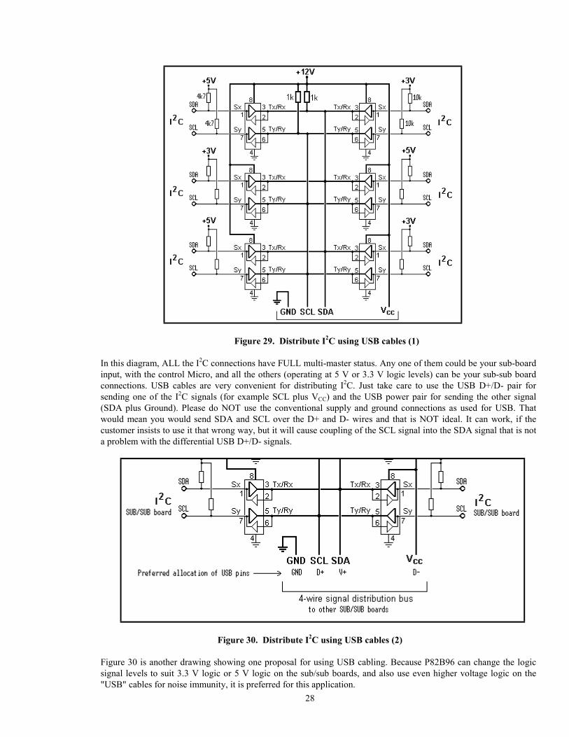
28
Figure 29. Distribute I2C using USB cables (1)
In this diagram, ALL the I2C connections have FULL multi-master status. Any one of them could be your sub-boardinput, with the control Micro, and all the others (operating at 5 V or 3.3 V logic levels) can be your sub-sub boardconnections. USB cables are very convenient for distributing I2C. Just take care to use the USB D+/D- pair forsending one of the I2C signals (for example SCL plus VCC) and the USB power pair for sending the other signal(SDA plus Ground). Please do NOT use the conventional supply and ground connections as used for USB. Thatwould mean you would send SDA and SCL over the D+ and D- wires and that is NOT ideal. It can work, if thecustomer insists to use it that wrong way, but it will cause coupling of the SCL signal into the SDA signal that is nota problem with the differential USB D+/D- signals.
Figure 30. Distribute I2C using USB cables (2)
Figure 30 is another drawing showing one proposal for using USB cabling. Because P82B96 can change the logicsignal levels to suit 3.3 V logic or 5 V logic on the sub/sub boards, and also use even higher voltage logic on the"USB" cables for noise immunity, it is preferred for this application.
29
4. Question: What is the maximum length of the cable that can be extended by the P82B715 or P82B96?Answer: Details can be found in Appendix 1 but a simple answer is that the maximum length depends on theSPEED that the bus operates and the type of cable that is used. For P82B715, we say that the limit is about 50meters and we recommend a clock speed slightly lower than 100 kHz is used.
In example 2) in Appendix 1, we show that 85 kHz is a very safe speed to operate with 50 meters of cable. ForP82B96, there is no maximum cable length because the bus capacitance limit does not apply and it is possible to addextra transistors to drive very long cables that are correctly terminated with their characteristic impedance. Inexample 3) in Appendix 1, we calculate that a cable length of 1 kilometer can be operated with a clock speed of 31kHz and a cable length of 100 meters can be safely operated at a speed of 71 kHz. Those calculations contain safetyfactors and the distances and speeds can be slightly higher. If the customer can tell us the actual I2C device numbersand the type of cables that will be used then we can calculate the limits that apply to their system.
5. Question: On a PCB, there are several I2C devices connected to one I2C bus. I want to extend the I2C bus byconnecting two further I2C devices using a ribbon cable. Because of the capacity of the ribbon cable (about 50 pF/m)I want to separate it with a PCA9515. The pull-up resistors for the SDA and SCL lines are on the PCB.
PCB with I2C bus ↔ PCA9515 ↔ pull-up resistors ↔ connector ↔ ribbon cable ↔ first I2C device ↔ ribbon cable↔ second I2C device
According to the I2C specs the low level output voltage VOL for an I2C device is 0.4 V @ 3 mA sink current. TheVOL of the PCA9515 is typically 0.5 V, but to recognize an Acknowledge sent by an I2C device, the voltage level ofSDA has to be 0.4 V max. This is OK for short distances between PCA9515 and I2C device. But what about thevoltage drop caused by the connector and the ribbon cable? Further, the I2C specifications recommend a seriesresistor Rs for the SDA / SCL input of the I2C device to protect it against high voltage spikes. There's also a voltagedrop (e.g. 100 x 3 mA = 300 mV = 0.3 V) that is too much / not allowed for the PCA9515. Conclusion: I cannot usethe PCA9515 in my application. Is this assumption correct?Answer: You are correct when you conclude that it is not good practice to try to signal over 'long' cable with thespecial logic levels that we need to use to prevent bi-directional I2C buffer ICs from latching like what is used on thePCA9515/16/18. That is why the P82B96 has those special logic levels on only ONE side and the other side usesperfectly conventional (CMOS style) logic levels with that logic threshold set at half the device's supply (VCC).You are free to choose any voltage you wish for VCC on P82B96 (2 V to 15 V) and this does not change the logicinterface signal levels on the special logic interface side. So you are able to interface to 5 V logic or, with a littlecare, even 3.3 V logic. As you say, those special levels are OK for short distances (e.g., on one circuit board). TheP82B715 uses an 'analog' amplification approach to permit inclusion of more cabling. It effectively reduces thesystem capacitance contribution of the cable to 1/10 its actual capacitance. It does not change the logic voltages.
6. Question: For our application, we want to send 3.3V I2C from our microcontroller over long cables to several slaveboards. How do we choose between P82B96 and P82B715?Answer:1) The main microcontroller has 3.3 V logic. If 3.3 V logic is sent over cables in a noisy environment, it is easy forthe noise to cause spurious bus signals. The interference only needs to be about 1.0 V to 1.5 V to cause wrongsignals. We propose to feed that 3.3 V logic into P82B96 and change it to 12 V logic signals. Then interfering noisesignals must cause 6 V signals on the cables before they can cause any wrong logic signals. If P82B715 was used,the logic signals must remain at 3.3 V, because P82B715 cannot change them. So the performance for noise will beabout 5 times worse than when using P82B96. When high immunity to noise is required, the P82B96 gives thatperformance. With the P82B96, it is allowed to have different logic levels on the slave boards. If some I2C devicesuse 5 V logic then P82B96 will change the 12 V logic on the cable to 5 V logic for those devices. With theP82B715, all devices in the system must use the same logic levels (or some extra circuits must be provided tochange the logic levels).
30
2) If the P82B715 is used, then the total system capacitance (after a special calculation for the cables) cannot bemore than the specification limit of 400 pF. The designer must add all the capacitance on every slave board and thenadd all the capacitance of all the cables. The total of all the capacitance (for all the boards), PLUS the total cablecapacitance divided by 10, must be less than 400 pF. That will put limits on the number of slave boards that can beconnected into one system. It also requires calculations. When the P82B96 is used, the only limitation is that eachseparate slave board (alone) must not exceed 400 pF. There is NO LIMIT on the capacitance of the wiring and NOLIMIT on the total system capacitance. It is allowed to connect any number of slave boards. The systemcalculations are much easier and changing the system is easy.
Electrical parameters
1. Question: What is the minimum and maximum frequency of the PCA9515?Answer: Since the PCA9515/16/18 are not clocked devices, the data sheet does not mention a clock frequency, butthey can operate up to 400 kHz depending on system timing requirements. An F-max for a buffer is hard to dealwith and it makes more sense to discuss the maximum toggle rate of the output. At the system level the principleissue is that the PCA9515/16/18 adds delays (170ns Tphl and 78ns Tplh). These delays aggravate the set-up andhold time requirements and also improve the edge rates that may or may not cancel out the delay. Thus, although allof the components in a system may be capable of operating at 400 kHz, the delay through the PCA9515/16/18 maycause set-up or hold time violations that limit system operation to something less than 400 kHz. ThePCA9515/16/18 are capable of running well above 400 kHz (input/ output toggle frequency and they are tested at a1 MHz frequency in final test) but a system with a PCA9515/16/18 in it may not be capable of 400 kHz. The devicescannot be used to connect a bus running at 100 kHz to a bus running at 400 kHz since all the buses always need tobe operating at the same speed unless they are isolated from each other and a bus master is located on each of thesegments. Minimum speed is the minimum speed specified by the I2C protocol, which is 0 kHz.
2. Question: We want to use the I2C at 400 kHz. However if we use the P82B96, the data transfers will go down toless than 100 kHz right? We want to know the way to increase noise immunity without using the P82B96.Answer: We updated the P82B96 data sheet and moved the oscilloscope traces from Application Note AN460 intothe data sheet. They show P82B96 waveforms when operating at 624 kHz. We also added the feature "capable of400 kHz when system delay times permit" to the data sheet. The reason we do not generally say P82B96 is suitablefor 400 kHz is that it introduces some propagation delays and a system designer must check those delays areacceptable in a total system. I have just checked our PCA9564 parallel to I2C bus interface and we can claim theP82B96 can be used in systems using the PCA9564 and the delays of the P82B96 will NOT limit the system speed.PCA9564 can be run at its maximum speed of about 360kHz as a master, or 400kHz as a slave.If you can tell us ALL the ICs to be used in your system, and we can check their timings, then we can tell youwhether 400 kHz, including using the P82B96, is possible. Usually the problem is that the timings for ALL ICs arenot available. That is the only reason we can't publish P82B96 as ALWAYS suitable for 400 kHz. Some typicaltimings of various ICs are given in Appendix 7.
3. Question: Is the PCA9516 SMBus compatible?Answer: The PCA9515/16/18 and P82B96 are SMBus compatible with regard to the normal I2C component of theSMBus standard.
4. Question: Why cant’ the P82B715 be used with SMBus devices? I tried it and it works.Answer: The P82B715 was designed well before SMBus existed and it can't work with the SMBus 'weak' pull-down current (350 µA). It senses bus sink current with a comparator across a 30 Ω sense resistor and the sensethreshold level is almost the sink current level specified for the SMBus. Of course, it is virtually impossible todesign an SMBus logic driver with only 350 µA sink current and it would be surprising if they couldn’t sink 3 mA.The SMBus also allows relatively large series protection resistors in each device output. We have to recommenddesigning to published specs. Many SMBus devices (and all Philips SMBus devices) are specified to sink standardI2C currents (3 mA) so of course, those may be used provided series protection resistors comply with I2C.
5. Question: Can the PCA9516 VOL be improved too less than 0.5 V? The goal is to be around 0.3 V or less.Answer: The PCA9515/16/18 are specifically designed to drive a low of 0.5 V and the difference between thefamily 0.3 V low and the special 0.5 V low on the PCA9515/16/18 is used to prevent lockup and yet accommodate
31
arbitration and clock stretching. The 0.5 V low should still allow plenty of noise margin to the 0.3 x VDD inputthreshold of I2C functions even with VDD = 3.3 V (0.3 x 3 V = 0.9 V).
6. Question: I've been looking through the PCA9516 data sheet and have some questions/clarifications. To avoid abuffer output from driving its own inputs low, you set the input low threshold 70 mV (typical) below Vol. From thedata sheet how do I determine the max Vol my external master needs to ensure a logic low is seen on the bufferinput. I would assume min Vol - max Vilc. Am I overlooking something? We cannot daisy chain these devicescorrect?Answer: Yes, it is correct that buffer devices cannot be daisy-chained. Special logic levels are used to avoidlatching when there is a need to buffer/extend an I2C bus. The valid low level is specified as following: (Vol - maxVilc) = 0.47 – 0.07 = 0.4V.
7. Question: I saw a note about use of the PCA9515 in a generic multi-master I2C environment (2000 Jul 06) sayingthat: “In a generic I2C environment only one repeater can be used because the output of one repeater will not berecognized as a low for arbitration purpose by a second repeater.” Please explain why the repeater cannot be usedrepeatedly in the one I2C BUS. It is appreciated if you could explain the technical background.Answer: Two PCA9515 cannot be used in series because of the way these devices sense whether a low on the line isbeing driven externally (i.e., by a device on the bus connected to that segment) to the device or internal (i.e., by adevice on a bus connected to the opposite side of the device) to the device. A low on one end of the bus will not beseen as a low at the other end of the bus if it must travel through more then one repeater. If the buffer designallowed a ‘low’ on one side to cause a “normal” low on its other side then, because the device is symmetrical, it willpass that low back to the first side and just latch itself low. To avoid this, we introduced another special logic ‘low’level, created by the device. It looks like a ‘low’ for externally connected devices but it is really about 0.5 V. Alevel of 0.5 V is not recognized by the device itself as ‘low’ so it is not passed by the device. When a second deviceis connected in series its output ‘low’ of 0.5 V is not recognized at the input of the second device. The PCA9511 isbeing designed to be used in series. The P82B96 only uses special logic levels on ONE side. You can connectdevices in series or parallel if you use the side with normal logic (Tx/Rx). Note that two PCA9515 can be used inparallel if you have the configuration described in Figure 31, because slaves do not need to see the acknowledge,data, or clock-stretching from other slaves.
Master
PCA9515
PCA9515
Slave(s) only
Slave(s) only
OK
OK
Figure 31. Using PCA9515 for parallel branches
8. Question: Is it possible to pull up each I2C segment to a different supply voltage (3.3 V or 5 V)?Answer: Yes, the upstream and downstream segments can be pulled up to either 3.3 V or 5 V.
9. Question: I am powering the PCA9516 at 3.3 V, but the enable lines EN1 to EN4 would be at logic 5 V comingfrom another semiconductor device. The specification says that the PCA9516 inputs are 5 V tolerant. I just want toconfirm this.Answer: Yes, the enable and I2C inputs/outputs of the PCA9515/16/18 are 5 V tolerant even when powered at 3.3V VCC and allow a voltage up to 6.0 V.
10. Question: We are using the PCA9516 and are powering the device with 3.3 V. On the 1 Port, we have a 5 V I2CBus. On the 0 Port, we have a 3.3 V I2C Bus. With a hard low (nearly ZERO Volts) on the SDA line of the 0 Portwe get only 0.7 V to 0.8 V on the SDA line of the 1 Port. The spec says it should be 0.6 V maximum. We are using
32
2.2 kΩ pull-ups and have tried more than one device. While our system is working, we would like more noisemargin. What is you recommendation?Answer: The PCA9516 is tested for 6 mA at 0.6 V in production. The simulations indicate that the 0.6 V holds forcurrents well in excess of 10 mA. I do not know how you are getting the 0.7 V to 0.8 V that is being reported,because 2.2 kΩ at 5 V is only about 2.3 mA, and it should read < 0.6 V. Possible explanations may be an outputseries resistor of 50 Ω or more, ground offset of > 0.1 V, or a lot more current than expected. All three seemunlikely, however if the series resistor is present, which is a common technique, I would recommend removing it, orat least moving the pull-up so that the current does not have to flow through the series resistor. Ground offset orexcessive currents would require solutions but I do not know what to suggest. Another possibility is that a rise timeaccelerator is on the 5 V line and is causing contention with the PCA9516.
11. Question: Can I safely interface a buffer with TTL level logic (not CMOS input level as required for true I2C)? MyI2C master controller is inside a processor that is performing I2C protocol, but its input level is TTL. The big concernI have is the weak 0.8 V ‘low’ drive and the 0.6 V minimum ‘low’ input threshold on the P82B96. Is there anydevice that I can put in between the P82B96 and the processor input to take care of the level problem (i.e., a 0.8 Vdriven by P82B96 will become a 0.4 V low level for the processor)?Answer: Yes, there is mismatch of logic level specifications at interfaces between the P82B96 and Micros with TTLlevels when their I/O lines are used as I2C drive lines. Philips' Micros that feature an I2C interface provide I2Ccompatible CMOS levels for I2C bus pins so this mismatch situation will normally only occur when the Micros usedhave no hardware provision for I2C.
To avoid this logic level specification mismatch, and usually timing problems as well, we recommend that everyeffort is made to select a processor with a hardware I2C port whenever working in systems with buffer ICs. Inpractice, the theoretical mismatch with TTL is unlikely to cause any REAL problems and if we add components tocause a closer theoretical matching of the paper specifications this will actually degrade the REAL situation withregard to typical noise margins. A few precautions can minimize the chances of any problems:For best margins in this situation, try to run the P82B96 Sx side at its minimum specified pull-up current (200 µA).The P82B96 VOL of 0.75 V at 25 oC or 0.85 V at –25 oC. TTL switching levels for various families of logic orMicros normally range between 1.1 V and 1.5 V so, in practice, the levels produced by P82B96 (with a light pull-up) offer reasonable typical noise margins, but no guarantees. TTL usually guarantees a low of 0.4 V when sinking 1mA providing a guaranteed margin below the P82B96 input threshold of 0.65 V at 25 oC or 0.55 V at 75 oC. Theactual Micro LOW may be specified as 0.4 V, and its real saturation at 200 µA will probably be under 50 mV.However, ground currents flowing from other port pins of the micro will raise its ‘internal’ ground and therefore theactual voltage seen at the I2C buffer pin, so the real margin can be very small. The ‘low’ of 0.6 V driven byPCA9515/16/18 provides a guaranteed margin below the TTL requirement of 0.66 V (minimum for 3 V) but itsinput threshold (contention or repeated ‘low’ data) of < 0.4 V has a lower noise margin than P82B96 when driven bythe TTL output low level.
The only buffer that does not use special logic thresholds is P82B715. Although it cannot be used above 100 kHz, itmight offer the best compromise if processors with TTL levels must be used. It will not change the logic voltagelevels by more than 100 mV. Although we usually say it cannot increase the total I2C capacitance beyond 400 pF,there is a special application that allows around 3000 pF, see Appendix 2.
12. Question: About that parameter "Low Level Output, Vol”. In the PCA9515 device specification, May 13, 2002,page 6 the minimum "Vol" is stated as 0.47 V. In the Philips "I2C-Bus Specification, Version 2.1, Jan 2000", page35, the "Vol" is given as 0.4 V maximum. The test conditions indicated are slightly different, but can you explainwhy the device specification is worst than the Bus Specification Standard?
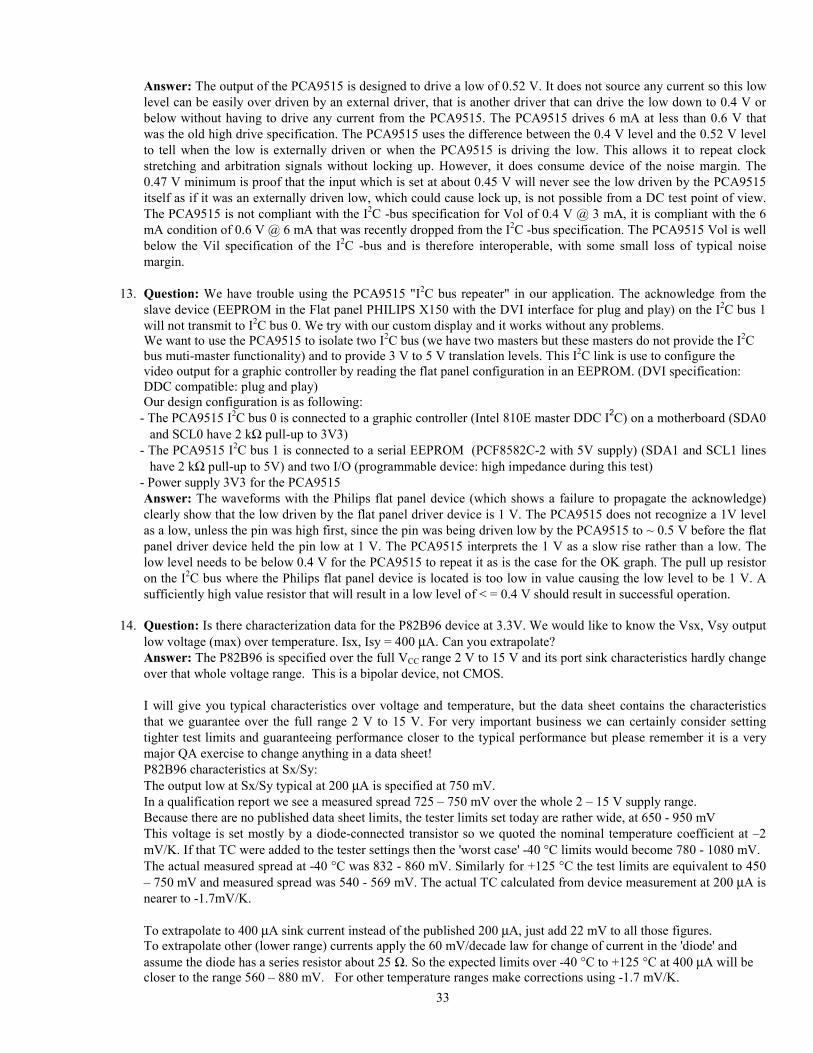
33
Answer: The output of the PCA9515 is designed to drive a low of 0.52 V. It does not source any current so this lowlevel can be easily over driven by an external driver, that is another driver that can drive the low down to 0.4 V orbelow without having to drive any current from the PCA9515. The PCA9515 drives 6 mA at less than 0.6 V thatwas the old high drive specification. The PCA9515 uses the difference between the 0.4 V level and the 0.52 V levelto tell when the low is externally driven or when the PCA9515 is driving the low. This allows it to repeat clockstretching and arbitration signals without locking up. However, it does consume device of the noise margin. The0.47 V minimum is proof that the input which is set at about 0.45 V will never see the low driven by the PCA9515itself as if it was an externally driven low, which could cause lock up, is not possible from a DC test point of view.The PCA9515 is not compliant with the I2C -bus specification for Vol of 0.4 V @ 3 mA, it is compliant with the 6mA condition of 0.6 V @ 6 mA that was recently dropped from the I2C -bus specification. The PCA9515 Vol is wellbelow the Vil specification of the I2C -bus and is therefore interoperable, with some small loss of typical noisemargin.
13. Question: We have trouble using the PCA9515 "I2C bus repeater" in our application. The acknowledge from theslave device (EEPROM in the Flat panel PHILIPS X150 with the DVI interface for plug and play) on the I2C bus 1will not transmit to I2C bus 0. We try with our custom display and it works without any problems.We want to use the PCA9515 to isolate two I2C bus (we have two masters but these masters do not provide the I2Cbus muti-master functionality) and to provide 3 V to 5 V translation levels. This I2C link is use to configure thevideo output for a graphic controller by reading the flat panel configuration in an EEPROM. (DVI specification:DDC compatible: plug and play)Our design configuration is as following:
- The PCA9515 I2C bus 0 is connected to a graphic controller (Intel 810E master DDC I2C) on a motherboard (SDA0and SCL0 have 2 kΩ pull-up to 3V3)
- The PCA9515 I2C bus 1 is connected to a serial EEPROM (PCF8582C-2 with 5V supply) (SDA1 and SCL1 lineshave 2 kΩ pull-up to 5V) and two I/O (programmable device: high impedance during this test)
- Power supply 3V3 for the PCA9515Answer: The waveforms with the Philips flat panel device (which shows a failure to propagate the acknowledge)clearly show that the low driven by the flat panel driver device is 1 V. The PCA9515 does not recognize a 1V levelas a low, unless the pin was high first, since the pin was being driven low by the PCA9515 to ~ 0.5 V before the flatpanel driver device held the pin low at 1 V. The PCA9515 interprets the 1 V as a slow rise rather than a low. Thelow level needs to be below 0.4 V for the PCA9515 to repeat it as is the case for the OK graph. The pull up resistoron the I2C bus where the Philips flat panel device is located is too low in value causing the low level to be 1 V. Asufficiently high value resistor that will result in a low level of < = 0.4 V should result in successful operation.
14. Question: Is there characterization data for the P82B96 device at 3.3V. We would like to know the Vsx, Vsy outputlow voltage (max) over temperature. Isx, Isy = 400 µA. Can you extrapolate?Answer: The P82B96 is specified over the full VCC range 2 V to 15 V and its port sink characteristics hardly changeover that whole voltage range. This is a bipolar device, not CMOS.
I will give you typical characteristics over voltage and temperature, but the data sheet contains the characteristicsthat we guarantee over the full range 2 V to 15 V. For very important business we can certainly consider settingtighter test limits and guaranteeing performance closer to the typical performance but please remember it is a verymajor QA exercise to change anything in a data sheet!P82B96 characteristics at Sx/Sy:The output low at Sx/Sy typical at 200 µA is specified at 750 mV.In a qualification report we see a measured spread 725 – 750 mV over the whole 2 – 15 V supply range.Because there are no published data sheet limits, the tester limits set today are rather wide, at 650 - 950 mVThis voltage is set mostly by a diode-connected transistor so we quoted the nominal temperature coefficient at –2mV/K. If that TC were added to the tester settings then the 'worst case' -40 °C limits would become 780 - 1080 mV.The actual measured spread at -40 °C was 832 - 860 mV. Similarly for +125 °C the test limits are equivalent to 450– 750 mV and measured spread was 540 - 569 mV. The actual TC calculated from device measurement at 200 µA isnearer to -1.7mV/K.
To extrapolate to 400 µA sink current instead of the published 200 µA, just add 22 mV to all those figures.To extrapolate other (lower range) currents apply the 60 mV/decade law for change of current in the 'diode' andassume the diode has a series resistor about 25 Ω. So the expected limits over -40 °C to +125 °C at 400 µA will becloser to the range 560 – 880 mV. For other temperature ranges make corrections using -1.7 mV/K.
34
It is not worthwhile trying to make any corrections for 3.3 V because the change over 2 – 15 V is too small.
When the customer needs those limits they are probably interested in the input threshold at Sx.There are limits published in the data sheet but for background here are the typical values.Again this is diode-based and has typical spreads...-40 °C: 757 mV -787 mV+25 °C: 635 mV - 648 mV+125 °C: 425 mV - 466 mVThe TC calculated from the mean values at –40 oC/+125 °C is -2.03 mV/K
15. Question: Can you give more ESD rating information on the P82B715 and P82B96 as they are intended forapplications including long cables and the potential for an operator picking up static electricity walking on the carpetand then picking up and plugging in a cable?Answer: The devices had to pass the usual qualification testing before release. Human Body Model testing todayuses both polarity pulses in 500 V steps to 3500 V, source impedance 100 pF/1500 ohms, on all I/O pins. MachineModel tests run 1000 V with virtually no series resistance. That is severe, but still cannot compare with a humancharged to 20 kV or even more! Design to withstand extremes of ESD requires attention to system design. PCBlayout is important, the discharge paths for the ‘lightning-like’ high pulse currents are not always easy to predict.But the design of these bipolar devices means it is RELATIVELY easy to apply effective protection using externalcomponents when conditions justify this. Results from the qualification report for P82B96 show the breakdownvoltage of the Sx pins ranged 27 V – 37 V at 5 mA. That is described as an LVceo or Vceo (sust) test wherebreakdown is first forced using a higher voltage and the device 'sustains' that voltage with 5 mA flowing. For the Txpins the 5 mA LVceo mean value was 46 V. This means that the I/Os can be protected against quite extremeconditions by applying series resistors and shunt Zeners that can have relatively high voltages. The figure shows anexample of a module that will be hot-plugged to a bus. The protection components are shown in Figure 32.
Figure 32. Hot Plug Example
In this example, a ‘module’ containing, for example, an I2C EEPROM device will be ‘hot plugged’ into equipmentwith power on and the I2C bus already active.Hardware requirements are:a) Cause no disturbance to the main running I2C bus (no glitches to ‘low’)b) Ensure the SDA/SCL lines of the EEPROM follow the rise of the EEPROM supply rail with no ‘glitches’ to
‘low’ that could result from activity on the main equipment’s I2C busc) Provide effective ESD protection for the I2C devices in the module, for safer handling.Meeting a) requires that the bus must not be pulled low by, e.g., diodes to the supply rail inside the EEPROM deviceduring the time the module supply is being charged from zero to proper operating supply. (-- Or even just fromcharging the stray capacitance of the module bus lines from zero volts). This is achieved by delaying application ofsupply to P82B96 until after the EEPROM supply is valid. Without supply, the P82B96 will open circuit its I/Olines. At worst, the active I2C bus must charge the stray capacitance of the C15 Zener (about 30 pF) and P82B96input (about 5 pF). When the supply/ground connections can be arranged to mate before the bus lines, ‘precharging’the Zener and P82B96 input can prevent even small ‘dips’ on the main I2C bus, assuming it is high. Requirement 2)is also met because P82B96 releases Rx/Tx so the pull-ups on the EEPROM will cause the SDA/SCL lines to followthe rising supply. The 15 V tolerant I/Os of P82B96 allow ESD protection using high voltage Zeners having muchlower capacitance than low voltage ones. (In any case 5 V devices cannot be protected by 5 V Zeners). Small series
LVC1G
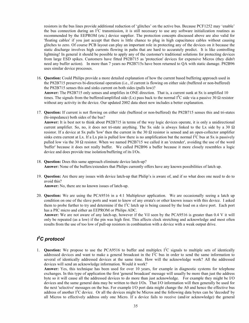
35
resistors in the bus lines provide additional reduction of ‘glitches’ on the active bus. Because PCF1252 may ‘enable’the bus connection during an I2C transmission, it is still necessary to use any software initialization routines asrecommended by the EEPROM (etc.) device supplier. The protection concepts discussed above are also valid for'floating cables' if you just accept that there is little chance to plug in high capacitance cables without causingglitches to zero. Of course PCB layout can play an important role in protecting any of the devices on it because thestatic discharge involves high currents flowing in paths that are hard to accurately predict. It is like controllinglightning! In general it should be possible to apply any of the customer's traditional solutions for protecting devicesfrom large ESD spikes. Customers have fitted P82B715 as 'protection' devices for expensive Micros (they didn'tneed any buffer action). In more than 7 years no P82B715s have been returned to QA with static damage. P82B96uses similar device processes.
16. Question: Could Philips provide a more detailed explanation of how the current based buffering approach used inthe P82B715 preserves bi-directional operation (i.e., if current is flowing on either side (buffered or non-buffered)the P82B715 senses this and sinks current on both sides (pulls low)?Answer: The P82B715 only senses and amplifies in ONE direction. That is, a current sunk at Sx is amplified 10times. The signals from the buffered/amplified side (Lx) pass back to the normal I2C side via a passive 30 Ω resistorwithout any activity in the device. Our updated 2002 data sheet now includes a better explanation.
17. Question: If current is not flowing on either side (buffered or non-buffered) the P82B715 senses this and tri-states(hi-impedance) both sides of the bus?Answer: It is best not to think about P82B715 in terms of the way logic devices operate, it is only a unidirectionalcurrent amplifier. So, no, it does not tri-state anything. The Sx side is always linked to the Lx side by a 30 Ωresistor. If a device at Sx pulls 'low' then the current in the 30 Ω resistor is sensed and an open-collector amplifiersinks extra current at Lx. If a Lx pin is pulled low there is no amplification but the normal I2C bus at Sx is passivelypulled low via the 30 Ω resistor. When we named P82B715 we called it an 'extender', avoiding the use of the word'buffer' because it does not really buffer. We called P82B96 a buffer because it more closely resembles a logicdevice and does provide true isolation/buffering of its I/Os.
18. Question: Does this same approach eliminate device latch-up?Answer: None of the buffers/extenders that Philips currently offers have any known possibilities of latch up.
19. Question: Are there any issues with device latch-up that Philip’s is aware of, and if so what does one need to do toavoid this?Answer: No, there are no known issues of latch-up.
20. Question: We are using the PCA9516 in a 4:1 Multiplexer application. We are occasionally seeing a latch upcondition on one of the slave ports and want to know of any errata's or other known issues with this device. I askedthem to probe further to try and determine if the I2C latch up is being caused by the load on a slave port. Each porthas a PIC micro and either an EEPROM or Philips ADC.Answer: We are not aware of any latch-up, however if the Vil seen by the PCA9516 is greater than 0.4 V it willonly be repeated (as a low) if the pin was high first. This affects clock stretching and acknowledge and most oftenresults from the use of too low of pull-up resistors in combination with a device with a weak output drive.
I2C protocol
1. Question: We propose to use the PCA9516 to buffer and multiplex I2C signals to multiple sets of identicallyaddressed devices and want to make a general broadcast in the I2C bus in order to send the same information toseveral of identically addressed devices at the same time. How will the acknowledge work? All the addresseddevices will send an acknowledge information. Would it work?Answer: Yes, this technique has been used for over 10 years, for example in diagnostic systems for telephoneexchanges. In this type of application the first 'general broadcast' message will usually be more than just the addressbyte so it will cause all the addressed devices to do more than just acknowledge. For example they might be I/Odevices and the same general data may be written to their I/Os. That I/O information will then generally be used forthe next 'selective' messages on the bus. For example I/O port data might change the A0 and hence the effective busaddress of another I2C device. Or all the devices might be Micros and the following data bytes can be 'decoded' byall Micros to effectively address only one Micro. If a device fails to receive (and/or acknowledge) the general
36
broadcast then this usually becomes evident in the NEXT communications and the system software needs to bedesigned to do the necessary checking and correction. This is simply saying that an I2C acknowledge is nice, butmore secure communications should use techniques like writing data and immediately reading it back to be sure thetransmission was correct. For 'general broadcast' it is not possible to check the 'general' transmitted data that way, sothe checks need to be made on the actions that were expected to happen AFTER that first message.
2. Multi-part Question:Question 2-1: In the theory of operation, you refer to what appears to be a bus conflict as clock stretching. What isit?Answer 2-1: Yes: the event on the SCL line defined in the I2C specification as clock stretching looks like lowcontention, or since it is an open drain/open collector bus, it is also referred to as a "wired bus".
Question 2-2: What is the advantage?Answer 2-2: The advantage is that multiple independent masters can share the bus with a simple arbitration schemewithout the need for centralized control.
Question 2-3: The device can recognize if two inputs are being driven low. Does it do anything with thisinformation?Answer 2-3: When one is released and the other remains low it will hold the first input to the 0.5 V low, so that themaster(s) will know that the line is still low.
Question 2-4: We have a large skew in tphl-tplh, my assumption is that this will vary with load and needs to betaken into account when determining the worse case clock pulse skew?Answer 2-4: The tphl is usually faster than the tplh unless the RC is very small and the tphl is determined by theslew rate control in the driver and not by the capacitance. The tplh is a direct RC time constant so it is very sensitiveto the load. The clock skew should only need to consider the difference in load between SDA and SCL. Anyrepeater will slow down the bus frequency by extending the pulse width low and pulse width high time requirement.The pulse width low is stretched by the repeater itself but for the PCA9515 and PCA9516 the master needs to allowa longer than minimum pulse width high
Question 2-5: Is the test load 7 pF, 50 pF or 57 pF?Answer 2-5: The external load is 50 pF and the pin capacitance is about 7 pF so the reported numbers correspond toa total capacitance of 57 pF.
3. Question: For the PCA9516, I was wondering more specifically, if two or more enable pins see highs at the sametime, what would happen in the arbitration logic? The logic that is driving the I2C hub may have two or more enablepins high for a small period of time (ns).Answer: There is not any problem having more than one enable high at a time. Even all high at the same time is nota problem, as long as the enables change state after a stop and before a start, that is during a bus idle state. If youchoose to change the enable pins during a transaction, there are a number of possible problems associated with theincomplete / interrupted transaction. When the enable pin is taken low, it turns off the outputs associated with thatenable and the inputs coming from those pins. If the pins are high as in an idle state, everything remains high.However, if the pin was being driven low externally when disabled, the other pins will now rise because the logicsees a disabled pin the same as a high. If the pin being enabled is low (which it should not be), the internal logic willsee the low as a falling edge and will propagate to all the other enabled pins. If another pin is disabled shortly afterthe low pin is enabled, there will be a momentary low going glitch on the disabled pin. If the enable is changedduring a transaction, some I2C devices will see the incomplete transaction, some may be left with an incompletetransaction waiting for a completion and false start or stop conditions may be seen by some devices. Not all I2Cdevices tolerate these conditions well, thus the instruction is that the enable pins should only be changed duringan idle state. The PCA9516 enable pins are direct acting and switch the associated port on or off immediatelyindependent of transactions in progress. The internal logic drives all enabled pins (SDAn or SCLn) low when afalling pin is detected and holds them low until the last pin being driven low externally is released, provided that theexternally driven lows are below 0.4 V.
Architecture / Applications
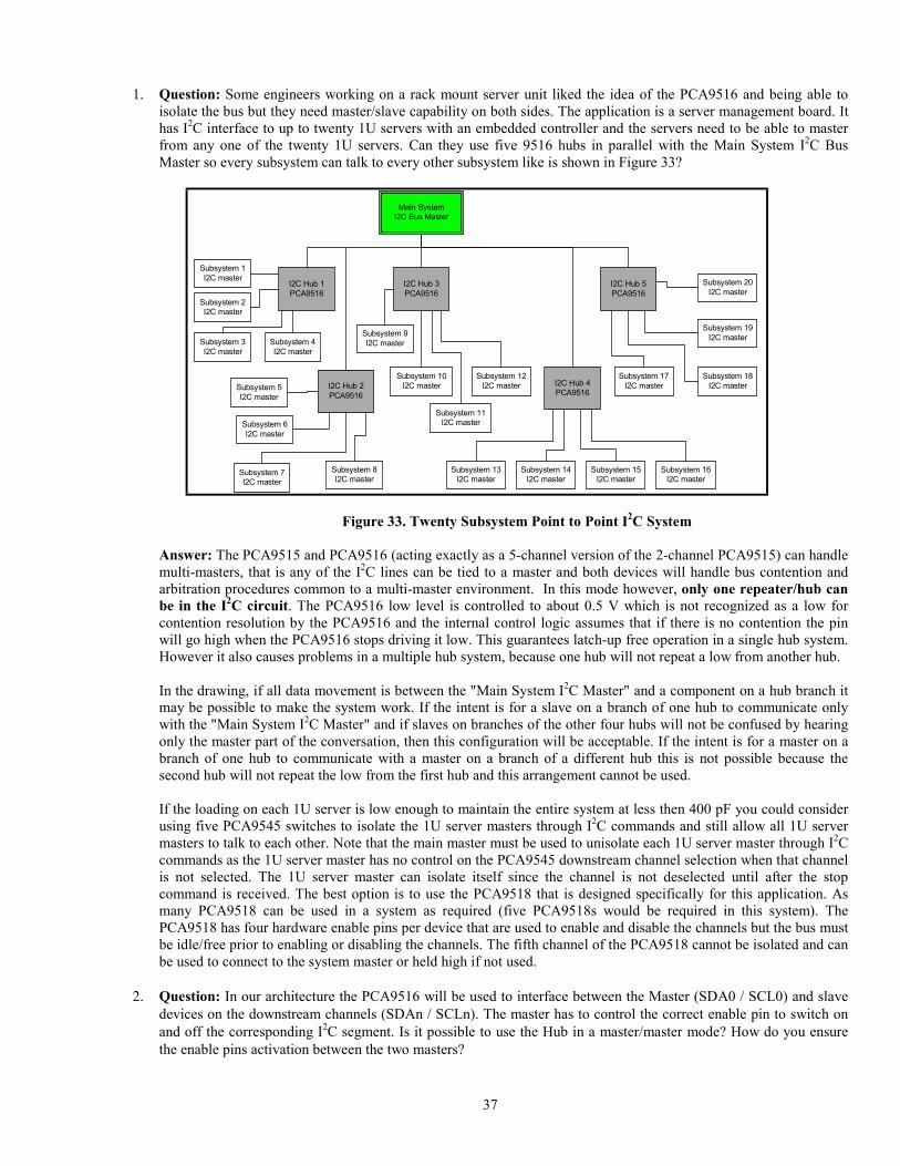
37
1. Question: Some engineers working on a rack mount server unit liked the idea of the PCA9516 and being able toisolate the bus but they need master/slave capability on both sides. The application is a server management board. Ithas I2C interface to up to twenty 1U servers with an embedded controller and the servers need to be able to masterfrom any one of the twenty 1U servers. Can they use five 9516 hubs in parallel with the Main System I2C BusMaster so every subsystem can talk to every other subsystem like is shown in Figure 33?
Main SystemI2C Bus Master
I2C Hub 1PCA9516
I2C Hub 2PCA9516
I2C Hub 3PCA9516
Subsystem 2I2C master
Subsystem 3I2C master
Subsystem 4I2C master
Subsystem 1I2C master
Subsystem 10I2C master
Subsystem 11I2C master
Subsystem 12I2C master
Subsystem 9I2C master
Subsystem 6I2C master
Subsystem 7I2C master
Subsystem 8I2C master
Subsystem 5I2C master
I2C Hub 4PCA9516
I2C Hub 5PCA9516
Subsystem 13I2C master
Subsystem 14I2C master
Subsystem 15I2C master
Subsystem 16I2C master
Subsystem 20I2C master
Subsystem 19I2C master
Subsystem 18I2C master
Subsystem 17I2C master
Figure 33. Twenty Subsystem Point to Point I2C System
Answer: The PCA9515 and PCA9516 (acting exactly as a 5-channel version of the 2-channel PCA9515) can handlemulti-masters, that is any of the I2C lines can be tied to a master and both devices will handle bus contention andarbitration procedures common to a multi-master environment. In this mode however, only one repeater/hub canbe in the I2C circuit. The PCA9516 low level is controlled to about 0.5 V which is not recognized as a low forcontention resolution by the PCA9516 and the internal control logic assumes that if there is no contention the pinwill go high when the PCA9516 stops driving it low. This guarantees latch-up free operation in a single hub system.However it also causes problems in a multiple hub system, because one hub will not repeat a low from another hub.
In the drawing, if all data movement is between the "Main System I2C Master" and a component on a hub branch itmay be possible to make the system work. If the intent is for a slave on a branch of one hub to communicate onlywith the "Main System I2C Master" and if slaves on branches of the other four hubs will not be confused by hearingonly the master part of the conversation, then this configuration will be acceptable. If the intent is for a master on abranch of one hub to communicate with a master on a branch of a different hub this is not possible because thesecond hub will not repeat the low from the first hub and this arrangement cannot be used.
If the loading on each 1U server is low enough to maintain the entire system at less then 400 pF you could considerusing five PCA9545 switches to isolate the 1U server masters through I2C commands and still allow all 1U servermasters to talk to each other. Note that the main master must be used to unisolate each 1U server master through I2Ccommands as the 1U server master has no control on the PCA9545 downstream channel selection when that channelis not selected. The 1U server master can isolate itself since the channel is not deselected until after the stopcommand is received. The best option is to use the PCA9518 that is designed specifically for this application. Asmany PCA9518 can be used in a system as required (five PCA9518s would be required in this system). ThePCA9518 has four hardware enable pins per device that are used to enable and disable the channels but the bus mustbe idle/free prior to enabling or disabling the channels. The fifth channel of the PCA9518 cannot be isolated and canbe used to connect to the system master or held high if not used.
2. Question: In our architecture the PCA9516 will be used to interface between the Master (SDA0 / SCL0) and slavedevices on the downstream channels (SDAn / SCLn). The master has to control the correct enable pin to switch onand off the corresponding I2C segment. Is it possible to use the Hub in a master/master mode? How do you ensurethe enable pins activation between the two masters?
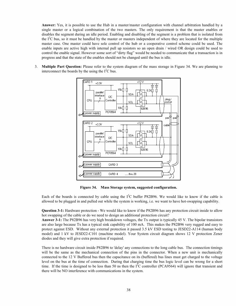
38
Answer: Yes, it is possible to use the Hub in a master/master configuration with channel arbitration handled by asingle master or a logical combination of the two masters. The only requirement is that the master enables ordisables the segment during an idle period. Enabling and disabling of the segment is a problem that is isolated fromthe I2C bus, so it must be handled by the master or masters independent of where they are located for the multiplemaster case. One master could have sole control of the hub or a cooperative control scheme could be used. Theenable inputs are active high with internal pull up resistors so an open drain / wired OR design could be used tocontrol the enable signal. However some sort of “dirty flag” would be needed to communicate that a transaction is inprogress and that the state of the enables should not be changed until the bus is idle.
3. Multiple Part Question: Please refer to the system diagram of the mass storage in Figure 34. We are planning tointerconnect the boards by the using the I2C bus.
Figure 34. Mass Storage system, suggested configuration.
Each of the boards is connected by cable using the I2C buffer P82B96. We would like to know if the cable isallowed to be plugged in and pulled out while the system is working, i.e. we want to have hot-swapping capability.
Question 3-1: Hardware protection - We would like to know if the P82B96 has any protection circuit inside to allowhot swapping of the cable or do we need to design an additional protection circuit?Answer 3-1: The P82B96 has very high breakdown voltages, the Tx output is typically 45 V. The bipolar transistorsare also large because Tx has a typical sink capability of 100 mA. This makes the P82B96 very rugged and easy toprotect against ESD. Without any external protection it passed 3.5 kV ESD testing to JESD22-A114 (human bodymodel) and 1 kV to JESD22-C101 (machine model). Your System circuit diagram shows 12 V protection Zenerdiodes and they will give extra protection if required.
There is no hardware circuit inside P82B96 to 'delay' any connections to the long cable bus. The connection timingswill be the same as the mechanical connection of the pins in the connector. When a new unit is mechanicallyconnected to the 12 V Buffered bus then the capacitance on its (buffered) bus lines must get charged to the voltagelevel on the bus at the time of connection. During that charging time the bus logic level can be wrong for a shorttime. If the time is designed to be less than 50 ns then the I2C controller (PCA9564) will ignore that transient andthere will be NO interference with communications in the system.
39
The system can be designed in different ways, but here is one suggestion. If it is possible to have the 12 V powersupply active on the board before the cable is plugged to the board then the Tx/Rx side of P82B96 will be pulledhigh by the bus pull-up resistors. When that board is connected to the cable bus then there are two possibilities:a) The bus is logic high (12 V) at that time. In this case there is no transient. No problem created.b) The bus is logic low (0 V) at that time. In this case the capacitance of the bus lines must be discharged from 12
V to 0 V by the P82B96 that is driving the bus low. There will be some positive spike on the bus but it isallowed to exceed 6 V (the logic threshold of P82B96) for 50 ns before the PCA9564 will recognize it becauseit has an input spike filter that rejects transients less than 50 ns.
Because P82B96 has about 100 mA sink capability it can discharge more than 800 pF to below 6 V in less than 50ns. The capacitance of one board, including Zeners and connectors, will be much less than 800 pF unless there arecables connected. So again there will be no problem. Perhaps we should claim "the combination of P82B96 +PCA9564 provides hardware protection for hot swapping when the board 12 V supply is active".If the board power supply is not active during hot-swap then its bus can be at 0 V. When joined to the cable bus atits high state there will be a transient low signal with a time determined by the board capacitance and the pull-uppresent on the system. If the pull-up was, say, 4 kΩ (there must be at least two other boards or there is no buscommunication to interrupt!) then it takes less than 20 pF stray capacitance to cause a false 'low' for >50 ns on thebus. If that causes problems in the PCA9564 then software will be needed to overcome the problem. This illustrateswhy it is better to have the 12 V present during hot-swap.
Question 3-2: Software protection - We understand that the I2C communication problems caused by hot swappingcan be prevented by the software design. Could you advise or provide know-how on the I2C software programming?Answer 3-2: We will try to get help for any particular problems that are found. The problems created by hot-swapmostly relate to the interruption of a message when the plug is pulled during a message. The 'master' will get novalid response from the 'slave' but the master will not ALWAYS know that invalid data has been provided. As oneexample, consider a master receiver is reading a data byte from a slave transmitter. If the plug is pulled in the middleof the data byte then the master thinks all following data bits are bus high level. The master transmitter provides theACK and the STOP so it does not know the slave was disconnected. It thinks the transmission was OK. Onlysoftware testing of the links can overcome that problem. As an example, if important data has been read then themaster can simply address the slave at the end of the data transfer and check for the acknowledge that means it isstill connected. For even more security the master can request a data byte from the slave (microcontroller) thatcontains a calculated 'checksum' for the data it just supplied.
Question 3-3: Power shut down of a board – What about the case that one of the boards of the system shuts down itspower for maintenance? We are concerned about power running into the board and would like to confirm thatP82B96 becomes high impedance when its power is down and does not inhibit the I2C bus.Answer 3-3: Yes, P82B96 releases all its I/Os to high impedance when VCC falls below typical 1.5 V. There are nopaths from any I/Os to the supply pin. Diodes in series with the pull-ups are needed to block this external path. Pull-ups on the Sx side to 5 V are OK but the supply to PCA9564 must be 3.3 V.If the 5 V supply fails on one card, but the 12 V supply remains active, then the 12 V bus lines will be pulled lowand the main 12 V bus cannot operate. If the 5 V supply is generated from the 12 V supply this should not be anyproblem. Another solution can be to use the voltage dividers shown, from the 12 V supply, instead of simple pull-ups on the 5 V interface. If the 3.3 V power supply (alone) fails then PCA9564 releases its SDA/SCL and will causeno system problem.
Question 3-4: Please confirm the driving capability of P82B96 allows these values:Number of the board in the system: 20Maximum length of the cable: 10 mDriving current of P82B96: 30 mACurrent sink required for each board: 1.5 mAI2C Pull up: 12 V, with a resistor of 8.2 kΩ
40
Answer 3-4: Yes, 30 mA is the static drive current for P82B96. The corresponding guaranteed low is 0.4 V. Thetypical drive capability is over 100 mA at 0.4 V. Having distributed pull-up resistors is a good idea because it makesall boards identical and adjusts the pull-up to the number of boards connected. Sinking the pull-up current of 20boards at 1.5 mA each is guaranteed by the data sheet, 30 mA static sink specification. There could be (speed)problems if 10 m were allowed for each board and the total cable was then 200 m. For 10 m, the longest cablepropagation delay is about 100 ns. That delay won’t cause any speed restriction in a 100 kHz system with onlyPCA9564 devices connected.
Question 3-5: We would like to confirm that under the condition above, the tr (1000 ns) and the tf (300 ns) at thedata rate of 100 kHz is guaranteed. Or do we need to compromise to reduce the transfer rate too less than 100 kHz?Answer 3-5: There will be no problems running the system at 100 kHz with PCA9564. The typical fall-time whenP82B96 is driving low is around 100 ns. As a guide, another customer wants to use P82B96 and opto-couplers in a400 kHz system. I think even that might be possible! The clock options for PCA9564 seem to be 90 kHz then 150kHz. You could even use 150 kHz provided the bus rise-times allow it.
The most significant timing limitation will probably be the buffered bus rise-time. With 8.2 kΩ resistors, the normalmaximum bus capacitance for 100 kHz would be about 120 – 150 pF. If 20 cables make up the 10 m total lengththen the average is 0.5 m cable. The cable capacitance will be only about 40 pF. The connectors + board traces +Zener + P82B96 might be about 50 - 60 pF total, so it looks OK. I would suggest using 15 V or 16 V Zeners (e.g.BZX284-C15) because they have lower capacitance than 12 V ones. If the ESD specifications of P82B96 aresufficient then Zeners are not necessary. I have found that the fast fall-times of P82B96 (less than 50 ns) can causeringing on the 12 V bus because it is not terminated in its characteristic impedance. A good way to prevent busundershoot is to fit small Schottky diodes like BAT54A to prevent negative swings and dissipate the energy (seeAppendix 5 for RC alternatives)
Question 3-6: Why do you introduce discussion of propagation delays in buffers when they are not found in the I2Cspecifications?Answer 3-6: For several customers wanting to expand their I2C systems, we need to introduce bus propagationdelays into the SCL and SDA signals but the existing I2C specifications do not expect bus delays, they were writtenabout small systems inside one enclosure. So I2C devices that "conform" to 100 kHz or 400 kHz bus specificationsare allowed to use up ALL of the available timing windows allowed in the I2C specifications and that means it is notpossible to introduce any other propagation delays. But if we know the timings ACTUALLY needed for a certaingroup of I2C devices in a system, then we can calculate whether there are really margins available. For example, ifwe use faster 400 kHz devices in a 100 kHz system we should have margins available that allow us to introduceother delays.
In a system we want to suggest for our customers, the only I2C devices in the whole system are the PCA9564.There will be 20 of them used in a multi-master system as shown in Figure 34.This system will introduce two bus propagation delays:1. Delays caused by buffering with P82B962. Cable propagation delays up to about 100 ns. (That is what I call 'round trip' delays, meaning the sum of SCL
delays from master to slave then the SDA delays back to the master. The total cable can be 10 meters long).The P82B96 delays include internal logic propagation delays (400 ns from master to slave and 400 ns slaveback to master) and effective propagation delays caused by bus rise and fall times on the long cables. The bussignals pass through two P82B96 devices that cause 300 + 100 ns for each direction. Because the delays will beidentical on the SCL and SDA lines, when the master supports 'clock stretching' then effectively about half thetotal introduced propagation delay does not need to be considered because the rise of the SCL line is delayed byP82B96. The SCL line at any one PCA9564 cannot rise until after ALL other sections of the bus systemtransporting the SCL signal have risen. Effectively, PCA9564 attempts to release SCL but it will not rise to alogic 'high' level until that 'attempt' to rise has propagated to the ends of the longest cable and back again. Thattotal delay time will be 400 ns for the P82B96 device delays, 100 ns for cable delays, and some allowance forbus rise times. Total stretch of SCL 'low' will be something over 500 ns. To design a system with introducedsignal delays, an important hardware timing is the time for a slave to output its valid data or an Acknowledge onits SDA line, following the falling edge of its SCL line that effectively 'requests' this response. The data mustbe available to the Master before/at the subsequent SCL rising edge. The timings simulated for PCA9564 aregiven in Appendix 7 and based on those timings, we can say that P82B96 and cable lengths of 10 meters willnot cause any reduction in the system speed limit (about 330 kHz for a Master)
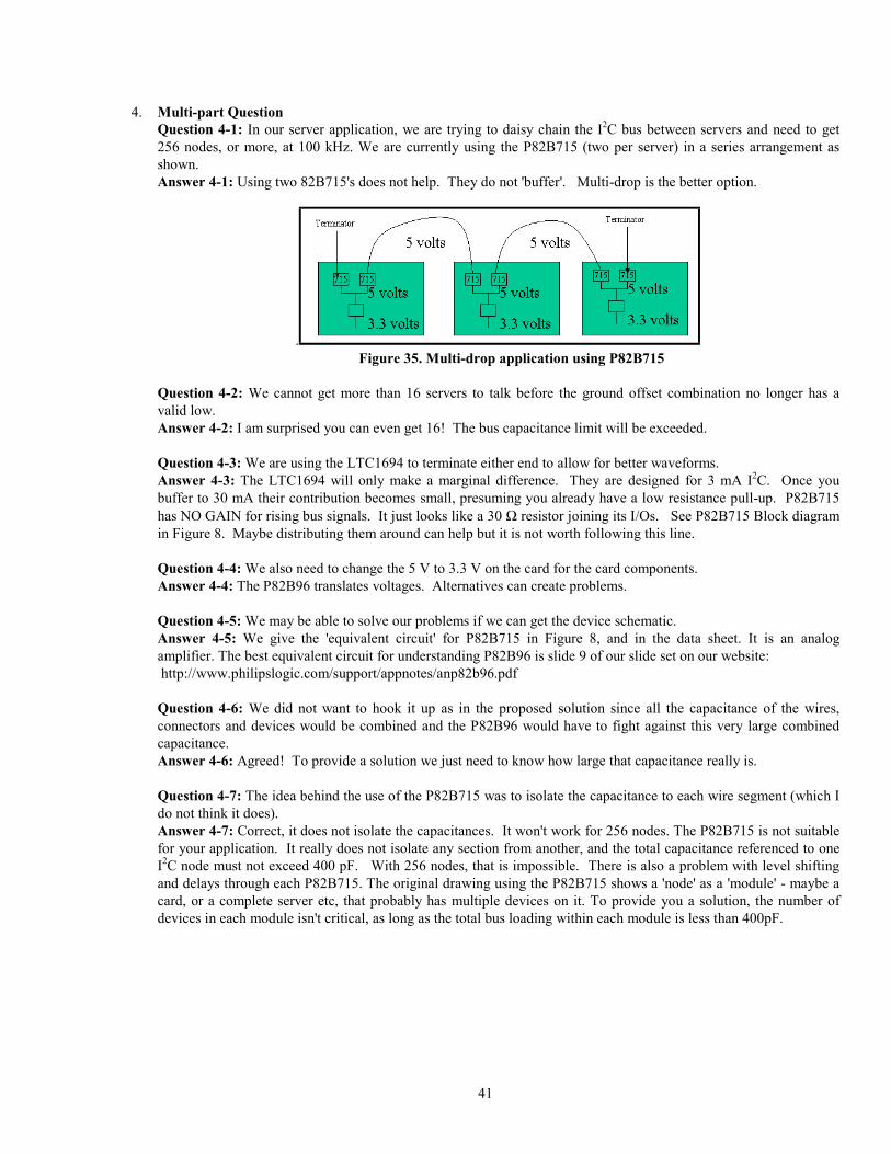
41
4. Multi-part QuestionQuestion 4-1: In our server application, we are trying to daisy chain the I2C bus between servers and need to get256 nodes, or more, at 100 kHz. We are currently using the P82B715 (two per server) in a series arrangement asshown.Answer 4-1: Using two 82B715's does not help. They do not 'buffer'. Multi-drop is the better option.
.Figure 35. Multi-drop application using P82B715
Question 4-2: We cannot get more than 16 servers to talk before the ground offset combination no longer has avalid low.Answer 4-2: I am surprised you can even get 16! The bus capacitance limit will be exceeded.
Question 4-3: We are using the LTC1694 to terminate either end to allow for better waveforms.Answer 4-3: The LTC1694 will only make a marginal difference. They are designed for 3 mA I2C. Once youbuffer to 30 mA their contribution becomes small, presuming you already have a low resistance pull-up. P82B715has NO GAIN for rising bus signals. It just looks like a 30 Ω resistor joining its I/Os. See P82B715 Block diagramin Figure 8. Maybe distributing them around can help but it is not worth following this line.
Question 4-4: We also need to change the 5 V to 3.3 V on the card for the card components.Answer 4-4: The P82B96 translates voltages. Alternatives can create problems.
Question 4-5: We may be able to solve our problems if we can get the device schematic.Answer 4-5: We give the 'equivalent circuit' for P82B715 in Figure 8, and in the data sheet. It is an analogamplifier. The best equivalent circuit for understanding P82B96 is slide 9 of our slide set on our website: http://www.philipslogic.com/support/appnotes/anp82b96.pdf
Question 4-6: We did not want to hook it up as in the proposed solution since all the capacitance of the wires,connectors and devices would be combined and the P82B96 would have to fight against this very large combinedcapacitance.Answer 4-6: Agreed! To provide a solution we just need to know how large that capacitance really is.
Question 4-7: The idea behind the use of the P82B715 was to isolate the capacitance to each wire segment (which Ido not think it does).Answer 4-7: Correct, it does not isolate the capacitances. It won't work for 256 nodes. The P82B715 is not suitablefor your application. It really does not isolate any section from another, and the total capacitance referenced to oneI2C node must not exceed 400 pF. With 256 nodes, that is impossible. There is also a problem with level shiftingand delays through each P82B715. The original drawing using the P82B715 shows a 'node' as a 'module' - maybe acard, or a complete server etc, that probably has multiple devices on it. To provide you a solution, the number ofdevices in each module isn't critical, as long as the total bus loading within each module is less than 400pF.
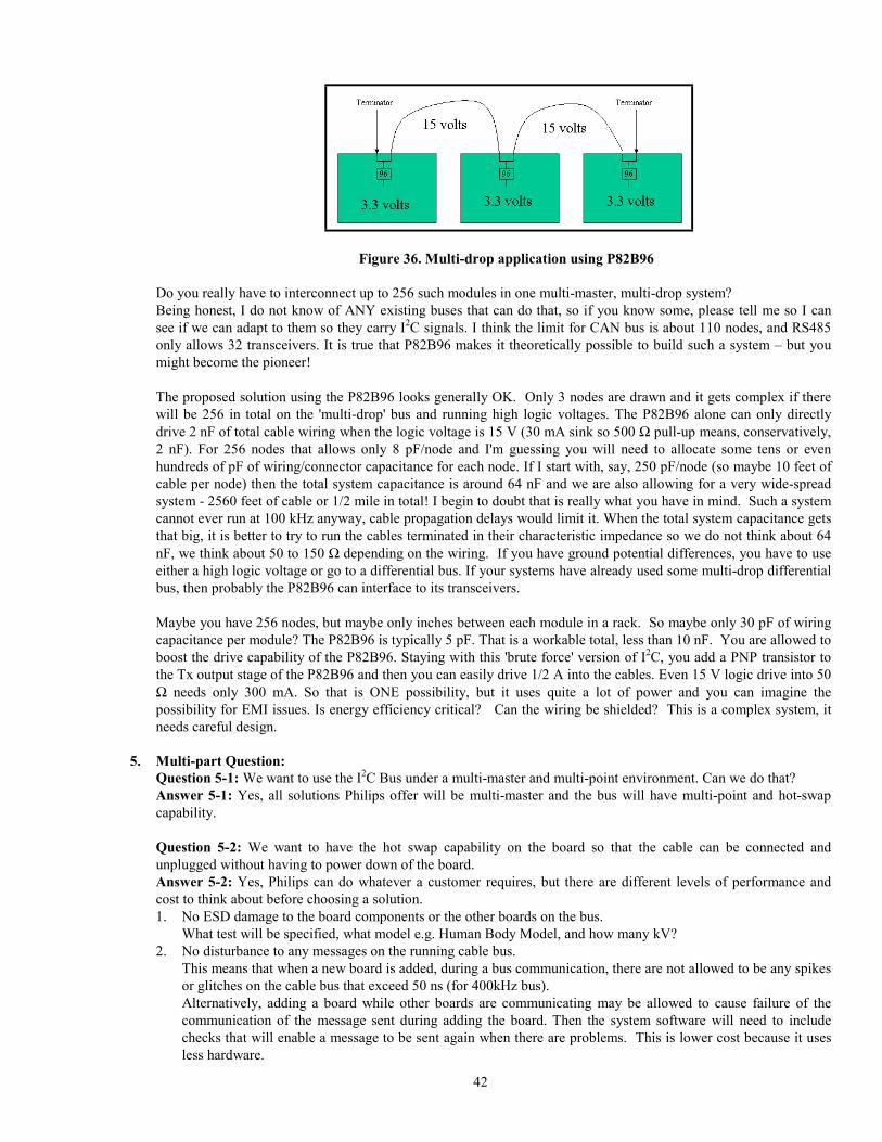
42
Figure 36. Multi-drop application using P82B96
Do you really have to interconnect up to 256 such modules in one multi-master, multi-drop system?Being honest, I do not know of ANY existing buses that can do that, so if you know some, please tell me so I cansee if we can adapt to them so they carry I2C signals. I think the limit for CAN bus is about 110 nodes, and RS485only allows 32 transceivers. It is true that P82B96 makes it theoretically possible to build such a system – but youmight become the pioneer!
The proposed solution using the P82B96 looks generally OK. Only 3 nodes are drawn and it gets complex if therewill be 256 in total on the 'multi-drop' bus and running high logic voltages. The P82B96 alone can only directlydrive 2 nF of total cable wiring when the logic voltage is 15 V (30 mA sink so 500 Ω pull-up means, conservatively,2 nF). For 256 nodes that allows only 8 pF/node and I'm guessing you will need to allocate some tens or evenhundreds of pF of wiring/connector capacitance for each node. If I start with, say, 250 pF/node (so maybe 10 feet ofcable per node) then the total system capacitance is around 64 nF and we are also allowing for a very wide-spreadsystem - 2560 feet of cable or 1/2 mile in total! I begin to doubt that is really what you have in mind. Such a systemcannot ever run at 100 kHz anyway, cable propagation delays would limit it. When the total system capacitance getsthat big, it is better to try to run the cables terminated in their characteristic impedance so we do not think about 64nF, we think about 50 to 150 Ω depending on the wiring. If you have ground potential differences, you have to useeither a high logic voltage or go to a differential bus. If your systems have already used some multi-drop differentialbus, then probably the P82B96 can interface to its transceivers.
Maybe you have 256 nodes, but maybe only inches between each module in a rack. So maybe only 30 pF of wiringcapacitance per module? The P82B96 is typically 5 pF. That is a workable total, less than 10 nF. You are allowed toboost the drive capability of the P82B96. Staying with this 'brute force' version of I2C, you add a PNP transistor tothe Tx output stage of the P82B96 and then you can easily drive 1/2 A into the cables. Even 15 V logic drive into 50Ω needs only 300 mA. So that is ONE possibility, but it uses quite a lot of power and you can imagine thepossibility for EMI issues. Is energy efficiency critical? Can the wiring be shielded? This is a complex system, itneeds careful design.
5. Multi-part Question:Question 5-1: We want to use the I2C Bus under a multi-master and multi-point environment. Can we do that?Answer 5-1: Yes, all solutions Philips offer will be multi-master and the bus will have multi-point and hot-swapcapability.
Question 5-2: We want to have the hot swap capability on the board so that the cable can be connected andunplugged without having to power down of the board.Answer 5-2: Yes, Philips can do whatever a customer requires, but there are different levels of performance andcost to think about before choosing a solution.1. No ESD damage to the board components or the other boards on the bus.
What test will be specified, what model e.g. Human Body Model, and how many kV?2. No disturbance to any messages on the running cable bus.
This means that when a new board is added, during a bus communication, there are not allowed to be any spikesor glitches on the cable bus that exceed 50 ns (for 400kHz bus).Alternatively, adding a board while other boards are communicating may be allowed to cause failure of thecommunication of the message sent during adding the board. Then the system software will need to includechecks that will enable a message to be sent again when there are problems. This is lower cost because it usesless hardware.
43
3. The board that is simply connected during a bus communication will receive only part of a message. It ispossible that a device receiving a part message can "lock up" and will require a special software message on thebus to re-set it.
There are different solutions:a) Hardware to prevent any ‘ends’ of messages being receivedb) Software solutions that will generate re-send messages when a board does not respond.
Question 5-3: We have a single-master, multi-drop distribution bus with P82B96 and we want to keep the main bussignals safe on our board even if an extension bus cable to any slave boards is pulled off accidentally.Answer 5-3: Which signals must be kept safe?a) The signals on the cable bus linking all the other boards that remain connected to the cable?
That is no problem. Those signals are safe.b) The signals on the board that is disconnected?
There can be a problem if the disconnection happens during a message to that board because the devices willkeep waiting for the message to end, and no end will come. This can only be handled by special software. Thedevices on the disconnected board (that remains powered but loses bus signals) might require a reset messageafter the bus is re-connected. When the slave board message is interrupted the master might not receive any‘acknowledge’. In that case the master knows there was a problem. If the master was reading the last byte ofdata when the break happens then it cannot know about the break (because the master provides theacknowledge). So after this transfer the master must send a new message and test for acknowledge. Then itknows if the slave connection was broken. It must send recovery messages and poll the slave address untilcommunication is restored.
Question 5-4: We want to design our I2C bus to be trouble free even if one of the power supplies of the board isshutdown, so it will not make any trouble to the bus and to the other boards.Answer 5-4: Yes, it can be safe. We just arrange the power supply circuit of P82B96 so it causes bus disconnectionwhen its supply (or some other supply) is removed. No problems when P82B96 is used as the bus interface. If adifferential bus is used we need to select the correct transceiver as in Question 5-5 below.
Question 5-5: We would like to use a differential bus drive to protect the bus from noise and EMS.Answer 5-5: Do you have special reasons to want a differential bus, or just good noise immunity is needed?When a differential bus is used it raises several difficulties:a) Twice as many bus wires needed in the cable and twice as many connection pins on the plugs and sockets.b) Every bus wire needs static damage protection components. So this doubles the number of protection
components.c) The differential bus driver/receiver devices will need to have a 'bus release' feature that guarantees no
disturbance to the differential bus if their power supply fails. I know there are several ICs like this, but you needto confirm this feature for the actual ICs that will be used. Philips’ CAN bus drivers have this feature. You willneed two drivers for every board (in addition to one P82B96 on each board). Part numbers are e.g. PCA82C251or TJA1040. Those CAN bus ICs, and most differential transceivers, require a 5V power supply. Is a 5V supplyavailable?
Do you have another differential bus transceiver device you would like to use and can you send a data sheet?Alternative proposal:Use the P82B96 to generate high voltage logic on the cables. If there is a 12 V supply then drive the cables with 12V logic signals. Is there any 12 V power supply available? The 12 V is only required at one place in the system, it isconvenient to send it to other places by using pairs of wires SCL + 12 V, SDA + ground. The bus 'noise margin' isthen around 6V because the logic threshold used by P82B96 is exactly half of VCC. That means it needs interferingsignals bigger than 6V coupled into the cables before there can be any wrong data. That noise performance isapproximately the same as CAN transceivers like PCA82C251, and still about half the guaranteed immunity of ournew devices like TJA1040. (I take the noise immunity limit as its maximum allowed common-mode voltage that is± 12 V for TJA1040)
6. Multi-part question: We are developing a mass storage system and there are 20 boards in the system. We want tocontrol these 20 boards using the I2C bus. Each board has its own Microcontroller. The architecture of each board islike this:Microcontroller → PCF8584 or PCA9564 → P82B715 or P82B96 → BUS, and all 20 boards have the samearchitecture.
44
Question 6-1: We want to use this I2C bus in a multi master environment (20 masters). Can the I2C Multiplexer beused as a way to eliminate addressing conflict?Answer 6-1: The I2C bus controller PCF8584 or PCA9564 has a 7-bit register where the designer can set theaddress of the device. So there can be up to 127 individual addresses and you could connect up to 127 boards in onesystem. 20 board application is not a problem and no multiplexer is needed. They can all connect to one bus. Asyou will see below, all the cards are allowed to connect to one "distribution" bus that has EXACTLY the samemulti-master operation as any standard I2C bus.
Question 6-2: We want to connect each board by a 5 meter maximum length cable and want to reduce noise. Weare thinking of using the P82B715 or P82B96. Can the P82B715 or P82B96 work in a multi master environment?Answer 6-2: I think there is only one choice, the P82B96, because I think the total system capacitance will be toobig for P82B715. With P82B96 there is NO limit on the total system capacitance. There could even be 127 boardsin one system.
Yes, both P82B96 and P82B715 work in a multi-master environment. They do not change any of the usual operationof the I2C Bus, they just extend its application to very big systems with large capacitance. For this application thecables between the boards can also use high voltage logic to have best noise immunity if there is any high voltagesupply available. Perhaps +12 V? It is best to use at least 5 V, but the P82B96 can use any voltage in the range 2 Vto 15 V. In a server application for another customer we just used 3.3 V on some 2 foot long cables and there wereno problems. I still recommend using 5 V or higher if there is a power supply available.
Question 6-3: When one of the boards in the system has trouble (e.g., power down or stops working), does thisaffect the operation of the other boards with a multi-drop bus architecture like this?Answer 6-3: When using the P82B96 to drive the cables between boards it is very simple to add some simple logicgates to test the power supplies and to isolate any card that has a power failure. It is not as easy to build a systemthat can detect a failure of one of the I2C devices anywhere in the system, but it is certainly possible if the systemdesigner adds some low cost logic and writes some dedicated software routines for each microcontroller. Themicrocontroller must be able to detect a general failure, for example by attempting to send a message. If a busfailure is detected then the microcontroller must disconnect its card (power down its P82B96) and test again. If thefault is still present then the fault is on its own card and it can keep its P82B96 powered down so this faulty card isisolated and the rest of the system can run. Other cards must then recognize that one card is not responding and raisean alarm to have that board repaired. That is only a simple example to explain one system protection. The totalsystem reliability depends on the software and there are many more techniques to improve reliability.
Question 6-4: We want to have hot-swapping capability for the boards. How do we add hot-swap to this busarchitecture?Answer 6-4: If I understand correctly, the cards do not simply plug into a rack, there are also long cables andconnectors in the system. The P82B96 offers a big system advantage when trying to hot-plug the cables/boards. SeeQuestion 15 on Page 34 for an example of some system design techniques. Today there are newer reset ICs thanPCF1252 in our range, but their function is the same.
Question 6-5: For differential bus driving with the P82B96, is there some additional device required other than theP82B96?Answer 6-5: If you want to use differential signaling on the cables then we can provide solutions for this. But firstwe should explain that just using a higher logic voltage on the cables makes a simpler solution for working in anoisy environment. If a differential bus is required then we need to know your preferred bus driver for the system.
Question 6-6: Don’t the connection made by the P82B715 or P82B96 break the rules of I2C? The addressing andmulti-master modes of the I2C bus do not work in the cable connected to P82B96?
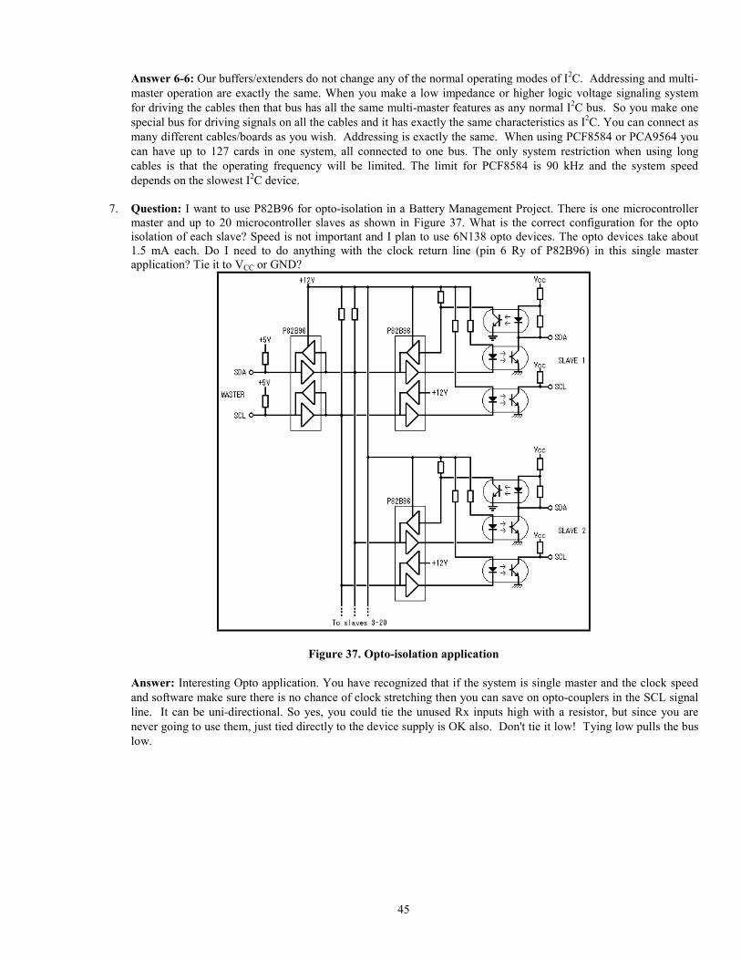
45
Answer 6-6: Our buffers/extenders do not change any of the normal operating modes of I2C. Addressing and multi-master operation are exactly the same. When you make a low impedance or higher logic voltage signaling systemfor driving the cables then that bus has all the same multi-master features as any normal I2C bus. So you make onespecial bus for driving signals on all the cables and it has exactly the same characteristics as I2C. You can connect asmany different cables/boards as you wish. Addressing is exactly the same. When using PCF8584 or PCA9564 youcan have up to 127 cards in one system, all connected to one bus. The only system restriction when using longcables is that the operating frequency will be limited. The limit for PCF8584 is 90 kHz and the system speeddepends on the slowest I2C device.
7. Question: I want to use P82B96 for opto-isolation in a Battery Management Project. There is one microcontrollermaster and up to 20 microcontroller slaves as shown in Figure 37. What is the correct configuration for the optoisolation of each slave? Speed is not important and I plan to use 6N138 opto devices. The opto devices take about1.5 mA each. Do I need to do anything with the clock return line (pin 6 Ry of P82B96) in this single masterapplication? Tie it to VCC or GND?
Figure 37. Opto-isolation application
Answer: Interesting Opto application. You have recognized that if the system is single master and the clock speedand software make sure there is no chance of clock stretching then you can save on opto-couplers in the SCL signalline. It can be uni-directional. So yes, you could tie the unused Rx inputs high with a resistor, but since you arenever going to use them, just tied directly to the device supply is OK also. Don't tie it low! Tying low pulls the buslow.
46
The arrangement is slightly unusual, but certainly allowed. The Master drives the 'distribution bus' with its 30 mAstatic capability but any slave has to drive this bus with its nominal I2C interface side (Sx). Fortunately on a 12 Vdistribution bus the bus 'low' level hardly matters. Low is anything less than 6 V. The Sx side of P82B96 isguaranteed to sink 7 mA at a low of 2 V and in practice it will do it with a normal <1 V low. So I would recommendthat the distribution bus pull-ups be calculated for, say, 6 mA sink current. That is 2 kΩ pull-ups to 12 V. Thatshould be OK for about 1 nF (say < 10 meters) of wiring capacitance. If the bus and capacitance is small then youdo not need to waste energy and you can use larger resistance pull-ups. The cheapest, simplest interface in AN460really is very slow with 4N36 and the warning about 5 kHz should be taken seriously - for the values given and a 5V supply. 6N138 looks very up-market in its published specs, but I never tried a Darlington opto for this job.Should work well. Just monitor the waveforms around the opto devices and check they are doing what the dataimplies.
8. Question: How do you include Opto-isolators into the bus wiring?Answer: AN460 shows both low speed and 100 kHz opto-coupling circuit values using the P82B96. See also the“I2C Opto-Electrical Isolation” section of this application note.
9. Question: Could you please comment on 400 kHz Opto isolation applications?Answer: It is necessary to know the timing requirements of the devices used in the system. In particular theresponse time delays to data valid or acknowledges from slave devices. 400 kHz can be achieved, even with P82B96propagation delays, by using fast Opto-couplers as shown in Figure 25.
ADDITIONAL INFORMATION
The latest data sheets and IBIS models for the I2C and SMBus Repeater/Hub/Expander family of products and other I2Cand SMBus products can be found at the Philips Semiconductors website http://www.semiconductors.philips.com/i2c orthe Philips Semiconductors Logic Products Group website at http://www.philipslogic.com/i2c.
Only the Logic Product Groups website will include data sheets and IBIS models for new unreleased sampling I2Cdevices.
Software tools for most of Philips’ I2C products can be found at: http://semiconductors.philips.com/i2c/support
Additionnal technical support for the I2C and SMBus Repeater/Hub/Expander family of products and other I2C andSMBus products can be requested by e-mailing the question to: [email protected]
See Philips Application Note AN460 for further application information about P82B96See Philips Application Note AN10160-01 for further application information about PCA9511/12/13/14See Philips Application Note AN462 for further application information about PCA954x Multiplexers/SwitchesSee Philips Application Note AN10145-01 for further application information about GTL2000/02/10 Bi-Directional LowVoltage Translators
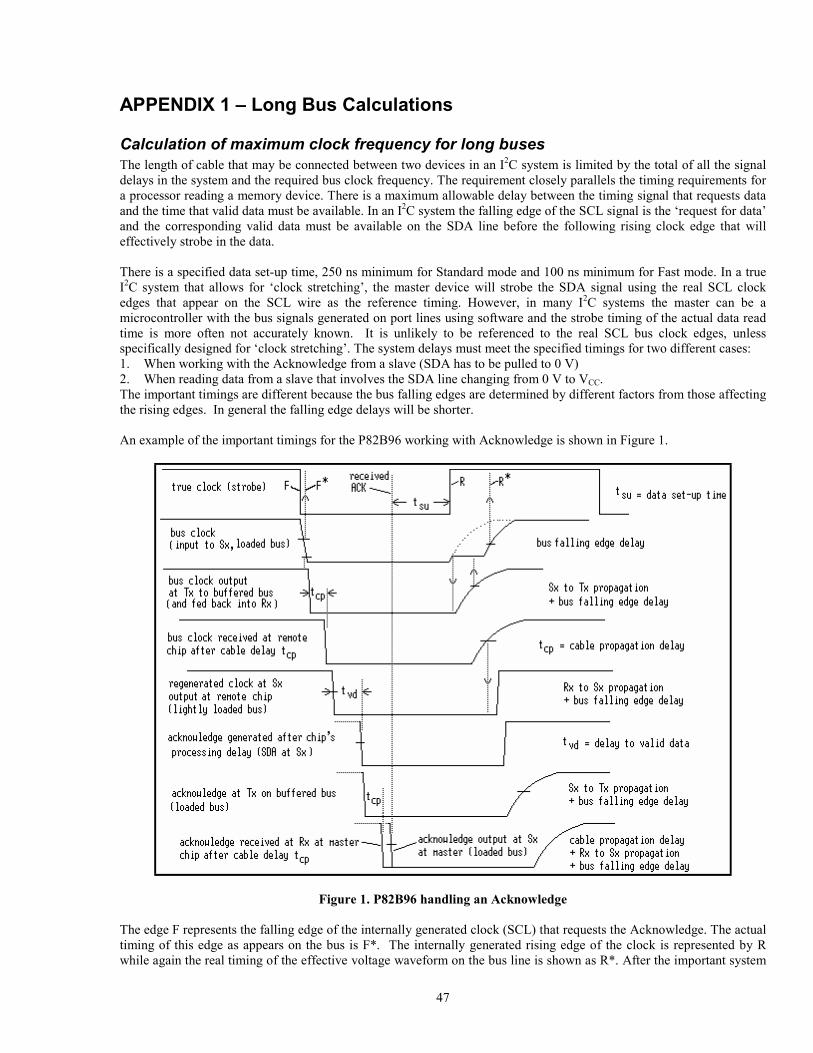
47
APPENDIX 1 – Long Bus Calculations
Calculation of maximum clock frequency for long busesThe length of cable that may be connected between two devices in an I2C system is limited by the total of all the signaldelays in the system and the required bus clock frequency. The requirement closely parallels the timing requirements fora processor reading a memory device. There is a maximum allowable delay between the timing signal that requests dataand the time that valid data must be available. In an I2C system the falling edge of the SCL signal is the ‘request for data’and the corresponding valid data must be available on the SDA line before the following rising clock edge that willeffectively strobe in the data.
There is a specified data set-up time, 250 ns minimum for Standard mode and 100 ns minimum for Fast mode. In a trueI2C system that allows for ‘clock stretching’, the master device will strobe the SDA signal using the real SCL clockedges that appear on the SCL wire as the reference timing. However, in many I2C systems the master can be amicrocontroller with the bus signals generated on port lines using software and the strobe timing of the actual data readtime is more often not accurately known. It is unlikely to be referenced to the real SCL bus clock edges, unlessspecifically designed for ‘clock stretching’. The system delays must meet the specified timings for two different cases:1. When working with the Acknowledge from a slave (SDA has to be pulled to 0 V)2. When reading data from a slave that involves the SDA line changing from 0 V to VCC.The important timings are different because the bus falling edges are determined by different factors from those affectingthe rising edges. In general the falling edge delays will be shorter.
An example of the important timings for the P82B96 working with Acknowledge is shown in Figure 1.
Figure 1. P82B96 handling an Acknowledge
The edge F represents the falling edge of the internally generated clock (SCL) that requests the Acknowledge. The actualtiming of this edge as appears on the bus is F*. The internally generated rising edge of the clock is represented by Rwhile again the real timing of the effective voltage waveform on the bus line is shown as R*. After the important system
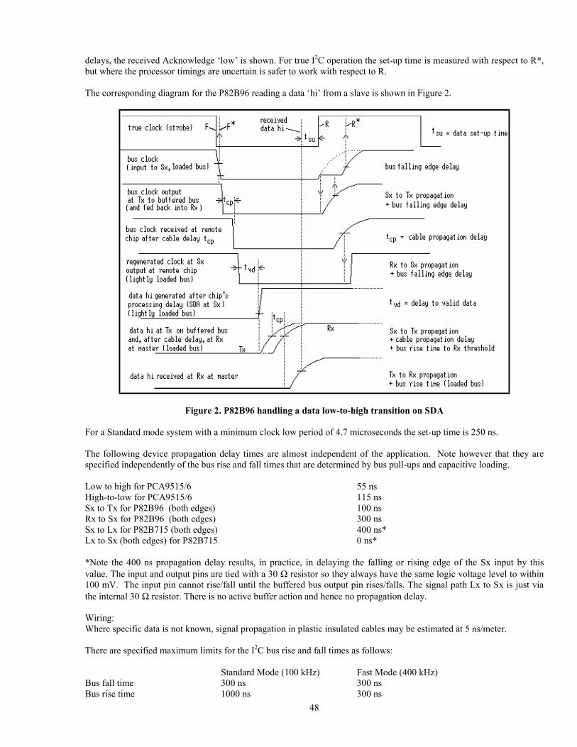
48
delays, the received Acknowledge ‘low’ is shown. For true I2C operation the set-up time is measured with respect to R*,but where the processor timings are uncertain is safer to work with respect to R.
The corresponding diagram for the P82B96 reading a data ‘hi’ from a slave is shown in Figure 2.
Figure 2. P82B96 handling a data low-to-high transition on SDA
For a Standard mode system with a minimum clock low period of 4.7 microseconds the set-up time is 250 ns.
The following device propagation delay times are almost independent of the application. Note however that they arespecified independently of the bus rise and fall times that are determined by bus pull-ups and capacitive loading.
Low to high for PCA9515/6 55 nsHigh-to-low for PCA9515/6 115 nsSx to Tx for P82B96 (both edges) 100 nsRx to Sx for P82B96 (both edges) 300 nsSx to Lx for P82B715 (both edges) 400 ns*Lx to Sx (both edges) for P82B715 0 ns*
*Note the 400 ns propagation delay results, in practice, in delaying the falling or rising edge of the Sx input by thisvalue. The input and output pins are tied with a 30 Ω resistor so they always have the same logic voltage level to within100 mV. The input pin cannot rise/fall until the buffered bus output pin rises/falls. The signal path Lx to Sx is just viathe internal 30 Ω resistor. There is no active buffer action and hence no propagation delay.
Wiring:Where specific data is not known, signal propagation in plastic insulated cables may be estimated at 5 ns/meter.
There are specified maximum limits for the I2C bus rise and fall times as follows:
Standard Mode (100 kHz) Fast Mode (400 kHz)Bus fall time 300 ns 300 nsBus rise time 1000 ns 300 ns
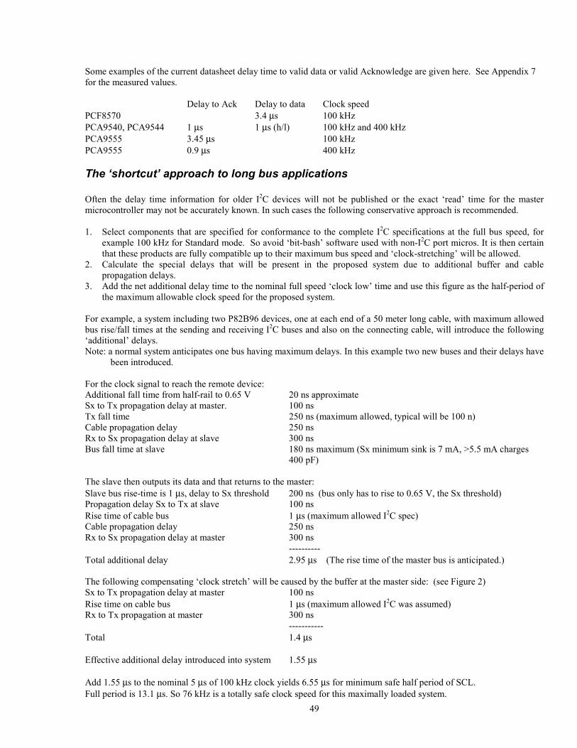
49
Some examples of the current datasheet delay time to valid data or valid Acknowledge are given here. See Appendix 7for the measured values.
Delay to Ack Delay to data Clock speedPCF8570 3.4 µs 100 kHzPCA9540, PCA9544 1 µs 1 µs (h/l) 100 kHz and 400 kHzPCA9555 3.45 µs 100 kHzPCA9555 0.9 µs 400 kHz
The ‘shortcut’ approach to long bus applications
Often the delay time information for older I2C devices will not be published or the exact ‘read’ time for the mastermicrocontroller may not be accurately known. In such cases the following conservative approach is recommended.
1. Select components that are specified for conformance to the complete I2C specifications at the full bus speed, forexample 100 kHz for Standard mode. So avoid ‘bit-bash’ software used with non-I2C port micros. It is then certainthat these products are fully compatible up to their maximum bus speed and ‘clock-stretching’ will be allowed.
2. Calculate the special delays that will be present in the proposed system due to additional buffer and cablepropagation delays.
3. Add the net additional delay time to the nominal full speed ‘clock low’ time and use this figure as the half-period ofthe maximum allowable clock speed for the proposed system.
For example, a system including two P82B96 devices, one at each end of a 50 meter long cable, with maximum allowedbus rise/fall times at the sending and receiving I2C buses and also on the connecting cable, will introduce the following‘additional’ delays.Note: a normal system anticipates one bus having maximum delays. In this example two new buses and their delays have
been introduced.
For the clock signal to reach the remote device:Additional fall time from half-rail to 0.65 V 20 ns approximateSx to Tx propagation delay at master. 100 nsTx fall time 250 ns (maximum allowed, typical will be 100 n)Cable propagation delay 250 nsRx to Sx propagation delay at slave 300 nsBus fall time at slave 180 ns maximum (Sx minimum sink is 7 mA, >5.5 mA charges
400 pF)
The slave then outputs its data and that returns to the master:Slave bus rise-time is 1 µs, delay to Sx threshold 200 ns (bus only has to rise to 0.65 V, the Sx threshold)Propagation delay Sx to Tx at slave 100 nsRise time of cable bus 1 µs (maximum allowed I2C spec)Cable propagation delay 250 nsRx to Sx propagation delay at master 300 ns
----------Total additional delay 2.95 µs (The rise time of the master bus is anticipated.)
The following compensating ‘clock stretch’ will be caused by the buffer at the master side: (see Figure 2)Sx to Tx propagation delay at master 100 nsRise time on cable bus 1 µs (maximum allowed I2C was assumed)Rx to Tx propagation at master 300 ns
-----------Total 1.4 µs
Effective additional delay introduced into system 1.55 µs
Add 1.55 µs to the nominal 5 µs of 100 kHz clock yields 6.55 µs for minimum safe half period of SCL.Full period is 13.1 µs. So 76 kHz is a totally safe clock speed for this maximally loaded system.
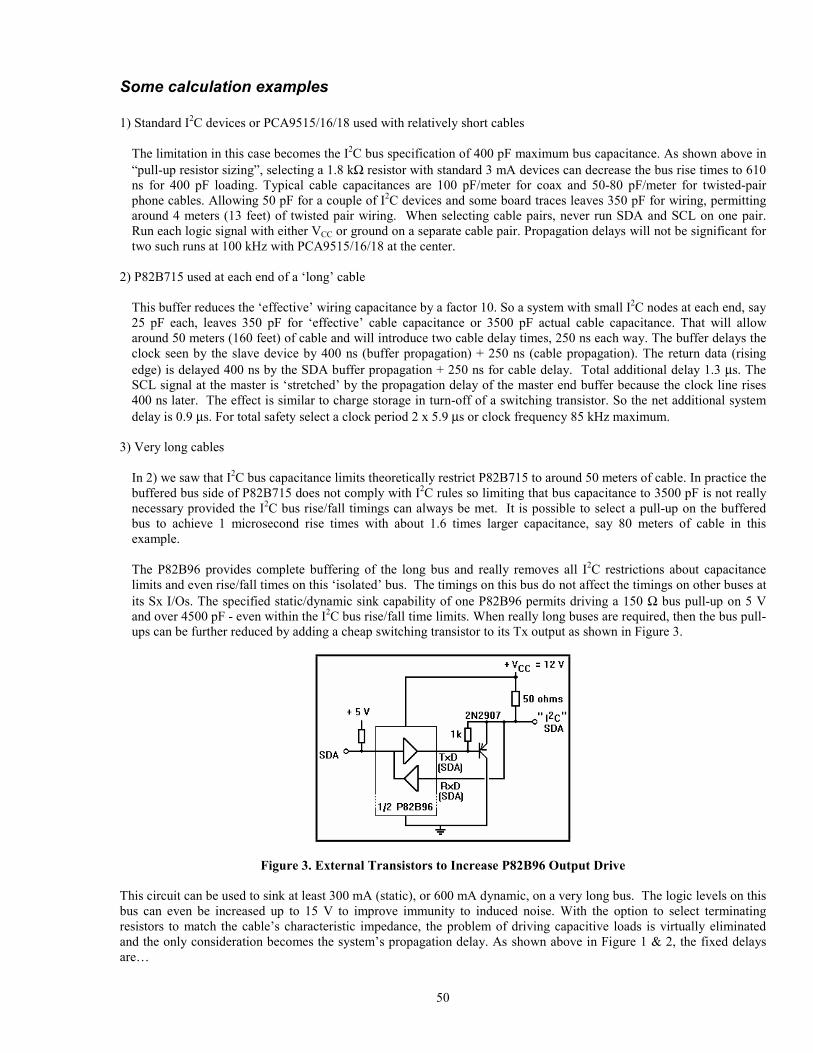
50
Some calculation examples
1) Standard I2C devices or PCA9515/16/18 used with relatively short cables
The limitation in this case becomes the I2C bus specification of 400 pF maximum bus capacitance. As shown above in“pull-up resistor sizing”, selecting a 1.8 kΩ resistor with standard 3 mA devices can decrease the bus rise times to 610ns for 400 pF loading. Typical cable capacitances are 100 pF/meter for coax and 50-80 pF/meter for twisted-pairphone cables. Allowing 50 pF for a couple of I2C devices and some board traces leaves 350 pF for wiring, permittingaround 4 meters (13 feet) of twisted pair wiring. When selecting cable pairs, never run SDA and SCL on one pair.Run each logic signal with either VCC or ground on a separate cable pair. Propagation delays will not be significant fortwo such runs at 100 kHz with PCA9515/16/18 at the center.
2) P82B715 used at each end of a ‘long’ cable
This buffer reduces the ‘effective’ wiring capacitance by a factor 10. So a system with small I2C nodes at each end, say25 pF each, leaves 350 pF for ‘effective’ cable capacitance or 3500 pF actual cable capacitance. That will allowaround 50 meters (160 feet) of cable and will introduce two cable delay times, 250 ns each way. The buffer delays theclock seen by the slave device by 400 ns (buffer propagation) + 250 ns (cable propagation). The return data (risingedge) is delayed 400 ns by the SDA buffer propagation + 250 ns for cable delay. Total additional delay 1.3 µs. TheSCL signal at the master is ‘stretched’ by the propagation delay of the master end buffer because the clock line rises400 ns later. The effect is similar to charge storage in turn-off of a switching transistor. So the net additional systemdelay is 0.9 µs. For total safety select a clock period 2 x 5.9 µs or clock frequency 85 kHz maximum.
3) Very long cables
In 2) we saw that I2C bus capacitance limits theoretically restrict P82B715 to around 50 meters of cable. In practice thebuffered bus side of P82B715 does not comply with I2C rules so limiting that bus capacitance to 3500 pF is not reallynecessary provided the I2C bus rise/fall timings can always be met. It is possible to select a pull-up on the bufferedbus to achieve 1 microsecond rise times with about 1.6 times larger capacitance, say 80 meters of cable in thisexample.
The P82B96 provides complete buffering of the long bus and really removes all I2C restrictions about capacitancelimits and even rise/fall times on this ‘isolated’ bus. The timings on this bus do not affect the timings on other buses atits Sx I/Os. The specified static/dynamic sink capability of one P82B96 permits driving a 150 Ω bus pull-up on 5 Vand over 4500 pF - even within the I2C bus rise/fall time limits. When really long buses are required, then the bus pull-ups can be further reduced by adding a cheap switching transistor to its Tx output as shown in Figure 3.
Figure 3. External Transistors to Increase P82B96 Output Drive
This circuit can be used to sink at least 300 mA (static), or 600 mA dynamic, on a very long bus. The logic levels on thisbus can even be increased up to 15 V to improve immunity to induced noise. With the option to select terminatingresistors to match the cable’s characteristic impedance, the problem of driving capacitive loads is virtually eliminatedand the only consideration becomes the system’s propagation delay. As shown above in Figure 1 & 2, the fixed delaysare…
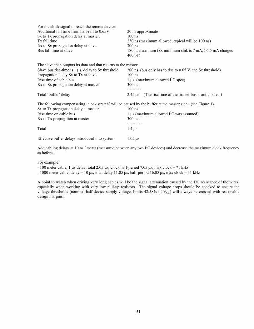
51
For the clock signal to reach the remote device:Additional fall time from half-rail to 0.65V 20 ns approximateSx to Tx propagation delay at master. 100 nsTx fall time 250 ns (maximum allowed, typical will be 100 ns)Rx to Sx propagation delay at slave 300 nsBus fall time at slave 180 ns maximum (Sx minimum sink is 7 mA, >5.5 mA charges
400 pF)
The slave then outputs its data and that returns to the master:Slave bus rise-time is 1 µs, delay to Sx threshold 200 ns (bus only has to rise to 0.65 V, the Sx threshold)Propagation delay Sx to Tx at slave 100 nsRise time of cable bus 1 µs (maximum allowed I2C spec)Rx to Sx propagation delay at master 300 ns
----------Total ‘buffer’ delay 2.45 µs (The rise time of the master bus is anticipated.)
The following compensating ‘clock stretch’ will be caused by the buffer at the master side: (see Figure 1)Sx to Tx propagation delay at master 100 nsRise time on cable bus 1 µs (maximum allowed I2C was assumed)Rx to Tx propagation at master 300 ns
-----------Total 1.4 µs
Effective buffer delays introduced into system 1.05 µs
Add cabling delays at 10 ns / meter (measured between any two I2C devices) and decrease the maximum clock frequencyas before.
For example:- 100 meter cable, 1 µs delay, total 2.05 µs, clock half-period 7.05 µs, max clock = 71 kHz- 1000 meter cable, delay = 10 µs, total delay 11.05 µs, half-period 16.05 µs, max clock = 31 kHz
A point to watch when driving very long cables will be the signal attenuation caused by the DC resistance of the wires,especially when working with very low pull-up resistors. The signal voltage drops should be checked to ensure thevoltage thresholds (nominal half device supply voltage, limits 42/58% of VCC) will always be crossed with reasonabledesign margins.
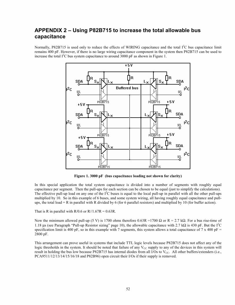
52
APPENDIX 2 – Using P82B715 to increase the total allowable buscapacitance
Normally, P82B715 is used only to reduce the effects of WIRING capacitance and the total I2C bus capacitance limitremains 400 pF. However, if there is no large wiring capacitance component in the system then P82B715 can be used toincrease the total I2C bus system capacitance to around 3000 pF as shown in Figure 1.
Figure 1. 3000 pF (bus capacitance loading not shown for clarity)
In this special application the total system capacitance is divided into a number of segments with roughly equalcapacitance per segment. Then the pull-ups for each section can be chosen to be equal (just to simplify the calculations).The effective pull-up load on any one of the I2C buses is equal to the local pull-up in parallel with all the other pull-upsmultiplied by 10. So in this example of 6 buses, and some system wiring, all having roughly equal capacitance and pull-ups, the total load = R in parallel with R divided by 6 (for 6 parallel resistors) and multiplied by 10 (for buffer action).
That is R in parallel with R/0.6 or R//1.67R = 0.63R.
Now the minimum allowed pull-up (5 V) is 1700 ohms therefore 0.63R =1700 Ω or R = 2.7 kΩ. For a bus rise-time of1.18 µs (see Paragraph “Pull-up Resistor sizing” page 10), the allowable capacitance with 2.7 kΩ is 430 pF. But the I2Cspecification limit is 400 pF, so in this example with 7 segments, this system allows a total capacitance of 7 x 400 pF =2800 pF.
This arrangement can prove useful in systems that include TTL logic levels because P82B715 does not affect any of thelogic thresholds in the system. It should be noted that failure of any VCC supply to any of the devices in this system willresult in holding the bus low because P82B715 has internal diodes from all I/Os to VCC. All other buffers/extenders (i.e.,PCA9511/12/13/14/15/16/18 and P82B96) open circuit their I/Os if their supply is removed.
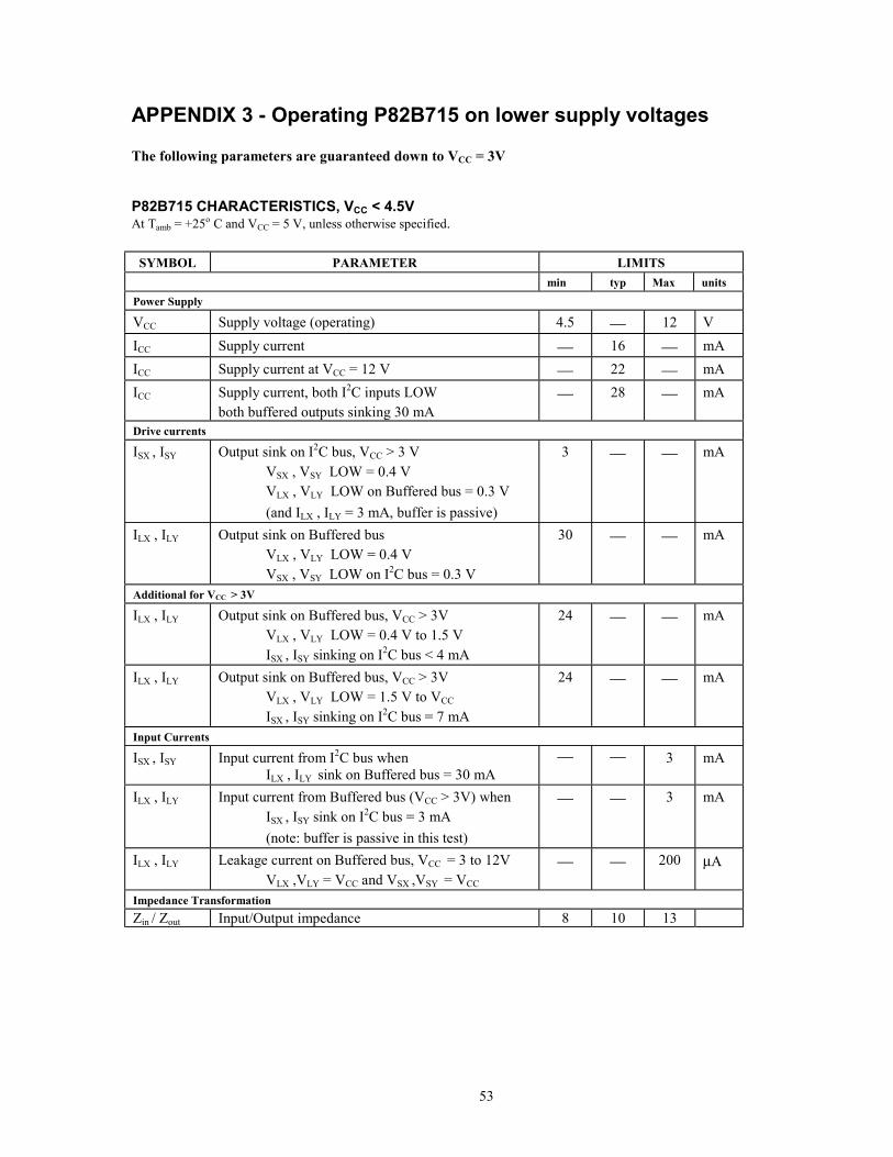
53
APPENDIX 3 - Operating P82B715 on lower supply voltages
The following parameters are guaranteed down to VCC = 3V
P82B715 CHARACTERISTICS, VCC < 4.5VAt Tamb = +25o C and VCC = 5 V, unless otherwise specified.
SYMBOL PARAMETER LIMITS
min typ Max units
Power Supply
VCC Supply voltage (operating) 4.5 12 V
ICC Supply current 16 mA
ICC Supply current at VCC = 12 V 22 mA
ICC Supply current, both I2C inputs LOWboth buffered outputs sinking 30 mA
28 mA
Drive currents
ISX , ISY Output sink on I2C bus, VCC > 3 V VSX , VSY LOW = 0.4 V VLX , VLY LOW on Buffered bus = 0.3 V
(and ILX , ILY = 3 mA, buffer is passive)
3 mA
ILX , ILY Output sink on Buffered bus VLX , VLY LOW = 0.4 V VSX , VSY LOW on I2C bus = 0.3 V
30 mA
Additional for VCC > 3V
ILX , ILY Output sink on Buffered bus, VCC > 3V VLX , VLY LOW = 0.4 V to 1.5 V ISX , ISY sinking on I2C bus < 4 mA
24 mA
ILX , ILY Output sink on Buffered bus, VCC > 3V VLX , VLY LOW = 1.5 V to VCC
ISX , ISY sinking on I2C bus = 7 mA
24 mA
Input Currents
ISX , ISY Input current from I2C bus when ILX , ILY sink on Buffered bus = 30 mA
3 mA
ILX , ILY Input current from Buffered bus (VCC > 3V) when ISX , ISY sink on I2C bus = 3 mA
(note: buffer is passive in this test)
3 mA
ILX , ILY Leakage current on Buffered bus, VCC = 3 to 12V VLX ,VLY = VCC and VSX ,VSY = VCC
200 µA
Impedance Transformation
Zin / Zout Input/Output impedance 8 10 13
54
APPENDIX 4 - The special logic levels and noise margins of buffer logic
There have been many attempts at making I2C buffers and opto-isolators. All result in (and most admit to) problemswith glitches resulting from signal propagation delays. They all block the signal propagation in one direction to preventlatch-up. So they all produce a ‘glitch’ during the signal propagation time needed to clear that blocking.
To test whether a buffer violates the I2C timings (due to glitches) apply this test:• Take one side low, take the other side low, and release the first side.• In a proper system the first side should just stay low, held by the second side. Switching-style buffers with timing
delays will all produce a ‘glitch’ to high on the first side before it goes low again.
To avoid glitches, one solution is to introduce ‘2 logic-low levels’ as the means to avoid latching of the buffer. That isthe approach used in the PCA9511/12/13/14/15/16/18 and P82B96. The P82B715 that does not use special logic levelsprovides uni-directional current amplification instead. The P82B96 uses only 'static' logic thresholds and responds onlyto DC levels. It has no 'memory' of previous I/O states. A ‘low’ at Sx will always be recognized and transmitted to Tx,but only when its DC level is below 0.65 V.
PCA9515, PCA9516 and PCA9518 feature ‘dynamic’ logic thresholds. In normal operation when simply passing logicsignals in either direction they uses conventional CMOS thresholds with typical switching at half VCC and published0.3/0.7 VCC limits. However while one input is driven low and its corresponding output is driven low by the device, toaround 0.5 V, the level at the output that is required to be recognized as a ‘low’ (for the bi-directional I2C signaling)becomes slightly lower than the 0.5 V driven by the device. This level, around 0.45 V, remains the low level inputthreshold UNTIL that output pin has been released and risen to above the CMOS ‘high’ level (typical 0.5 VCC, maximum0.7 VCC).
In an application where a master has just sent ‘low’ data bits to a slave on the SDA line, and then tries to read back anAcknowledge ‘low’ bit from the slave, it is quite possible that stray bus capacitance together with a quick response fromthe slave, will mean the SDA line will never cross the CMOS ‘high’ level before being clamped ‘low’ again by theAcknowledge from the slave*. In this case the EFFECTIVE logic low threshold, necessary for correct reading of thatAcknowledge ‘low’, is 0.45 V.
So the Sx input of P82B96 and all inputs of PCA9515/16/18 should be considered as having their low level input logicthresholds at around 0.65 V and 0.45 V respectively. While these thresholds are guaranteed by the I2C static low of 0.4 V(maximum) at 3 mA, and are the compromise that allows designing a non-latching bi-directional buffer, it should benoted that the noise margin is relatively small. Care must be taken when designing with these I/Os to ensure the systemnoise will not exceed this margin.
* [Acknowledge from a slave happens after the 8th SCL clock pulse. The falling edge of the 8th SCL clock pulse is thesignal to a slave to put an acknowledge 'low' on SDA before the rising edge of the 9th SCL clock pulse. The slaveresponse can be very fast, normally there is only a simple counter of the SCL pulses and the falling edge of SCL canresult in an almost immediate acknowledge 'low' on the slave's SDA. Consider the master had sent a data 'low' (viaPCA9515) so on the 8th clock pulse SDA0 was low and so was SDA1. SDA0 will be released by the master at (ormaybe just after) the falling edge of the 8th SCL pulse and will start to rise towards ‘high’. If SDA1 has near maximumbus loading it will rise 'slowly' with some time-constant, let's say 1 µs. Because SDA1 is the 'output', it is not recognizedas 'low' by PCA9515 during this slew towards VCC, until it has risen above a CMOS 'high' level. The only level that willbe recognized as low (before the line reaches ‘high’) is one that is below the original SDA1 output level, i.e. a true I2Clow, about 0.4 V. So when a slave places its acknowledge 'low' onto the SDA line, if this is not maintained below about0.4 V then this Acknowledge from the slave will not be maintained as a ‘low’ at SDA0. Any noise affecting the 0.4 Vlevel can appear as pulses to ‘high’ at SDA0. With some delay caused by capacitive loading on SDA1 and a fastacknowledge from the slave (as must be expected) it is most probable that the acknowledge will NOT get transmittedunless SDA1 can be held below about 0.4 V.]
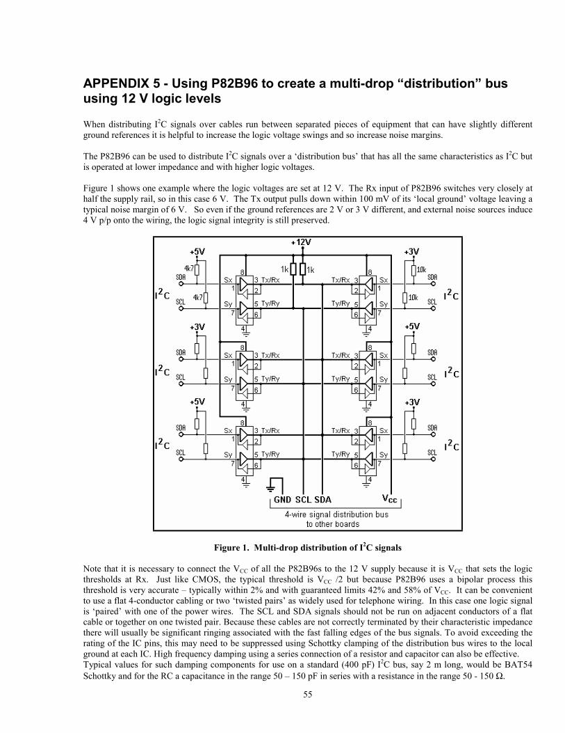
55
APPENDIX 5 - Using P82B96 to create a multi-drop “distribution” bususing 12 V logic levels
When distributing I2C signals over cables run between separated pieces of equipment that can have slightly differentground references it is helpful to increase the logic voltage swings and so increase noise margins.
The P82B96 can be used to distribute I2C signals over a ‘distribution bus’ that has all the same characteristics as I2C butis operated at lower impedance and with higher logic voltages.
Figure 1 shows one example where the logic voltages are set at 12 V. The Rx input of P82B96 switches very closely athalf the supply rail, so in this case 6 V. The Tx output pulls down within 100 mV of its ‘local ground’ voltage leaving atypical noise margin of 6 V. So even if the ground references are 2 V or 3 V different, and external noise sources induce4 V p/p onto the wiring, the logic signal integrity is still preserved.
Figure 1. Multi-drop distribution of I2C signals
Note that it is necessary to connect the VCC of all the P82B96s to the 12 V supply because it is VCC that sets the logicthresholds at Rx. Just like CMOS, the typical threshold is VCC /2 but because P82B96 uses a bipolar process thisthreshold is very accurate – typically within 2% and with guaranteed limits 42% and 58% of VCC. It can be convenientto use a flat 4-conductor cabling or two ‘twisted pairs’ as widely used for telephone wiring. In this case one logic signalis ‘paired’ with one of the power wires. The SCL and SDA signals should not be run on adjacent conductors of a flatcable or together on one twisted pair. Because these cables are not correctly terminated by their characteristic impedancethere will usually be significant ringing associated with the fast falling edges of the bus signals. To avoid exceeding therating of the IC pins, this may need to be suppressed using Schottky clamping of the distribution bus wires to the localground at each IC. High frequency damping using a series connection of a resistor and capacitor can also be effective.Typical values for such damping components for use on a standard (400 pF) I2C bus, say 2 m long, would be BAT54Schottky and for the RC a capacitance in the range 50 – 150 pF in series with a resistance in the range 50 - 150 Ω.
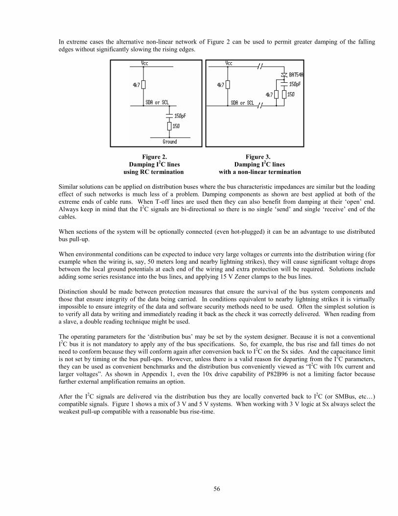
56
In extreme cases the alternative non-linear network of Figure 2 can be used to permit greater damping of the fallingedges without significantly slowing the rising edges.
Figure 2. Figure 3. Damping I2C lines Damping I2C lines
using RC termination with a non-linear termination
Similar solutions can be applied on distribution buses where the bus characteristic impedances are similar but the loadingeffect of such networks is much less of a problem. Damping components as shown are best applied at both of theextreme ends of cable runs. When T-off lines are used then they can also benefit from damping at their ‘open’ end.Always keep in mind that the I2C signals are bi-directional so there is no single ‘send’ and single ‘receive’ end of thecables.
When sections of the system will be optionally connected (even hot-plugged) it can be an advantage to use distributedbus pull-up.
When environmental conditions can be expected to induce very large voltages or currents into the distribution wiring (forexample when the wiring is, say, 50 meters long and nearby lightning strikes), they will cause significant voltage dropsbetween the local ground potentials at each end of the wiring and extra protection will be required. Solutions includeadding some series resistance into the bus lines, and applying 15 V Zener clamps to the bus lines.
Distinction should be made between protection measures that ensure the survival of the bus system components andthose that ensure integrity of the data being carried. In conditions equivalent to nearby lightning strikes it is virtuallyimpossible to ensure integrity of the data and software security methods need to be used. Often the simplest solution isto verify all data by writing and immediately reading it back as the check it was correctly delivered. When reading froma slave, a double reading technique might be used.
The operating parameters for the ‘distribution bus’ may be set by the system designer. Because it is not a conventionalI2C bus it is not mandatory to apply any of the bus specifications. So, for example, the bus rise and fall times do notneed to conform because they will conform again after conversion back to I2C on the Sx sides. And the capacitance limitis not set by timing or the bus pull-ups. However, unless there is a valid reason for departing from the I2C parameters,they can be used as convenient benchmarks and the distribution bus conveniently viewed as “I2C with 10x current andlarger voltages”. As shown in Appendix 1, even the 10x drive capability of P82B96 is not a limiting factor becausefurther external amplification remains an option.
After the I2C signals are delivered via the distribution bus they are locally converted back to I2C (or SMBus, etc…)compatible signals. Figure 1 shows a mix of 3 V and 5 V systems. When working with 3 V logic at Sx always select theweakest pull-up compatible with a reasonable bus rise-time.
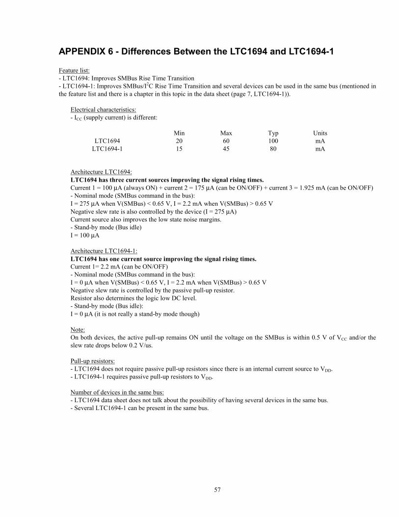
57
APPENDIX 6 - Differences Between the LTC1694 and LTC1694-1
Feature list:- LTC1694: Improves SMBus Rise Time Transition- LTC1694-1: Improves SMBus/I2C Rise Time Transition and several devices can be used in the same bus (mentioned inthe feature list and there is a chapter in this topic in the data sheet (page 7, LTC1694-1)).
Electrical characteristics:- ICC (supply current) is different:
Min Max Typ UnitsLTC1694 20 60 100 mA
LTC1694-1 15 45 80 mA
Architecture LTC1694:LTC1694 has three current sources improving the signal rising times.Current 1 = 100 µA (always ON) + current 2 = 175 µA (can be ON/OFF) + current 3 = 1.925 mA (can be ON/OFF)- Nominal mode (SMBus command in the bus):I = 275 µA when V(SMBus) < 0.65 V, I = 2.2 mA when V(SMBus) > 0.65 VNegative slew rate is also controlled by the device (I = 275 µA)Current source also improves the low state noise margins.- Stand-by mode (Bus idle)I = 100 µA
Architecture LTC1694-1:LTC1694 has one current source improving the signal rising times.Current 1= 2.2 mA (can be ON/OFF)- Nominal mode (SMBus command in the bus):I = 0 µA when V(SMBus) < 0.65 V, I = 2.2 mA when V(SMBus) > 0.65 VNegative slew rate is controlled by the passive pull-up resistor.Resistor also determines the logic low DC level.- Stand-by mode (Bus idle):I = 0 µA (it is not really a stand-by mode though)
Note:On both devices, the active pull-up remains ON until the voltage on the SMBus is within 0.5 V of VCC and/or theslew rate drops below 0.2 V/us.
Pull-up resistors:- LTC1694 does not require passive pull-up resistors since there is an internal current source to VDD.- LTC1694-1 requires passive pull-up resistors to VDD.
Number of devices in the same bus:- LTC1694 data sheet does not talk about the possibility of having several devices in the same bus.- Several LTC1694-1 can be present in the same bus.
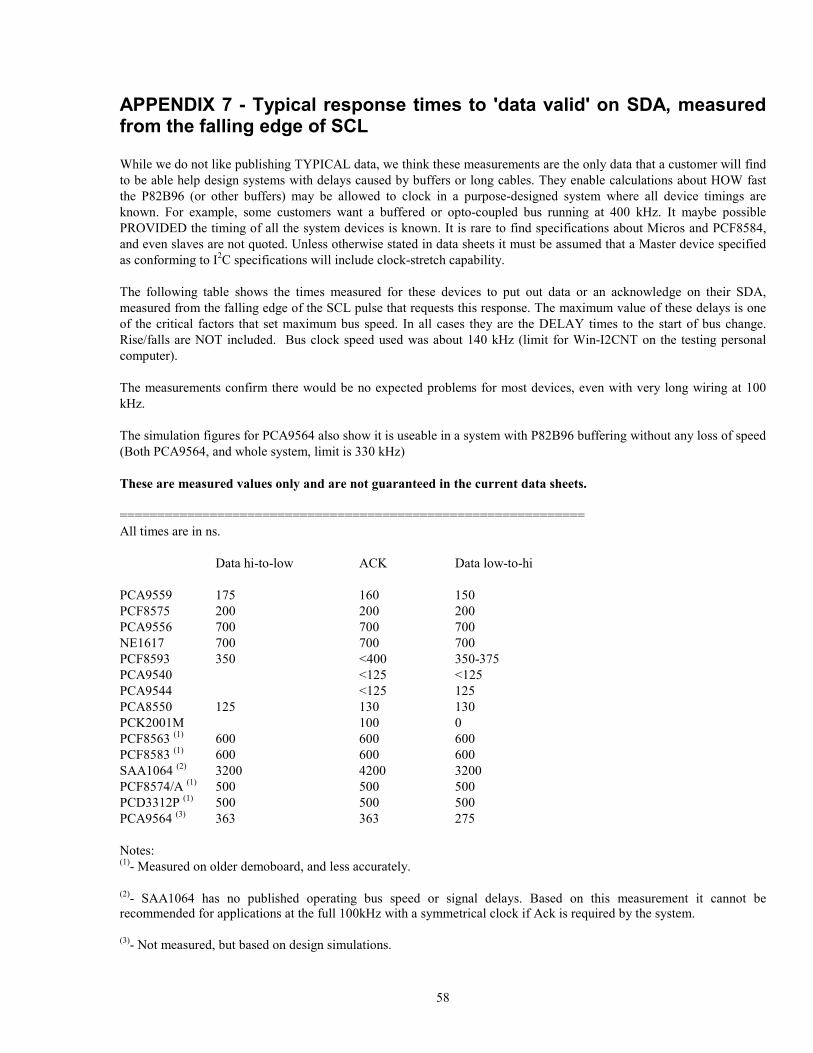
58
APPENDIX 7 - Typical response times to 'data valid' on SDA, measuredfrom the falling edge of SCL
While we do not like publishing TYPICAL data, we think these measurements are the only data that a customer will findto be able help design systems with delays caused by buffers or long cables. They enable calculations about HOW fastthe P82B96 (or other buffers) may be allowed to clock in a purpose-designed system where all device timings areknown. For example, some customers want a buffered or opto-coupled bus running at 400 kHz. It maybe possiblePROVIDED the timing of all the system devices is known. It is rare to find specifications about Micros and PCF8584,and even slaves are not quoted. Unless otherwise stated in data sheets it must be assumed that a Master device specifiedas conforming to I2C specifications will include clock-stretch capability.
The following table shows the times measured for these devices to put out data or an acknowledge on their SDA,measured from the falling edge of the SCL pulse that requests this response. The maximum value of these delays is oneof the critical factors that set maximum bus speed. In all cases they are the DELAY times to the start of bus change.Rise/falls are NOT included. Bus clock speed used was about 140 kHz (limit for Win-I2CNT on the testing personalcomputer).
The measurements confirm there would be no expected problems for most devices, even with very long wiring at 100kHz.
The simulation figures for PCA9564 also show it is useable in a system with P82B96 buffering without any loss of speed(Both PCA9564, and whole system, limit is 330 kHz)
These are measured values only and are not guaranteed in the current data sheets.
==============================================================All times are in ns.
Data hi-to-low ACK Data low-to-hi
PCA9559 175 160 150PCF8575 200 200 200PCA9556 700 700 700NE1617 700 700 700PCF8593 350 <400 350-375PCA9540 <125 <125PCA9544 <125 125PCA8550 125 130 130PCK2001M 100 0PCF8563 (1) 600 600 600PCF8583 (1) 600 600 600SAA1064 (2) 3200 4200 3200PCF8574/A (1) 500 500 500PCD3312P (1) 500 500 500PCA9564 (3) 363 363 275
Notes:(1)- Measured on older demoboard, and less accurately.
(2)- SAA1064 has no published operating bus speed or signal delays. Based on this measurement it cannot berecommended for applications at the full 100kHz with a symmetrical clock if Ack is required by the system.
(3)- Not measured, but based on design simulations.