hot-wire chemical vapour deposition of silicon carbide...
TRANSCRIPT
HOT-WIRE CHEMICAL VAPOUR DEPOSITION
OF SILICON CARBIDE THIN FILMS
FROM PURE SILANE AND METHANE GASES
FATEMEH SHARIATMADAR TEHRANI
FACULTY OF SCIENCE
UNIVERSITY OF MALAYA
KUALA LUMPUR
2013
HOT-WIRE CHEMICAL VAPOUR DEPOSITION
OF SILICON CARBIDE THIN FILMS
FROM PURE SILANE AND METHANE GASES
FATEMEH SHARIATMADAR TEHRANI
THESIS SUBMITTED IN FULFILLMENT OF
THE REQUIREMENT FOR THE DEGREE
OF DOCTOR OF PHILOSOPHY
DEPARTMENT OF PHYSICS
FACULTY OF SCIENCE
UNIVERSITY OF MALAYA
KUALA LUMPUR
2013
iii
ABSTRACT
A hot-wire chemical vapour deposition (HWCVD) system is a simple and cost-
effective technique for deposition of Si-based films. Silicon carbide (SiC) on the other
hand is a very interesting material with many unique properties. This work is directed
towards understanding how the structural properties of the SiC films affect the opto-
electronic properties of the films. This is important for application of this wide band gap
semiconductor as a window material in photovoltaic solar cells.
In this work, an HWCVD system built in the laboratory is successfully utilized
to grow multi-phased SiC films from silane (SiH4) and methane (CH4) gases without
hydrogen dilution. In the first part of this work, the influence of precursor gas
concentration on chemical bonding, crystallinity and elemental composition of the films
is studied. The precursor gas concentration is changed by depositing films at different
CH4 flow-rates with the SiH4 flow-rate fixed at SiH4 starving condition and at different
total gas partial pressures with the fixed ratio of SiH4 to CH4 flow-rate. In the second
part of this work, the effects of deposition pressure and substrate-to-filament distance on
the structural and optical properties of films are investigated. The deposition pressure
controls the residence time of precursor molecules in the reactor and the filament-to-
substrate distance determines the energy of the radicals reaching the growth sites. Then,
the structural properties of the films are studied with respect to the optical energy gap
(Eg), refractive index (n), and photoluminescence properties of the SiC films. The final
part of this work focuses on the growth mechanism of SiC films.
In this work, high quality SiC films have been successfully grown in the
HWCVD system. The highest growth rate of the SiC films achieved in this work is
higher than reported values for films grown by conventional deposition techniques. It is
established that the formation of SiC nano-crystals can be manipulated by controlling
the CH4 to SiH4 flow-rate ratio in SiH4 starving condition. It is also shown that an
optimum total gas partial pressure is required for the formation of SiC nano-crystalline
phases in the films. The decrease in filament-to-substrate distance is shown to promote
the formation of nano-crystalline SiC phases and hydrogenated amorphous carbon (a-
C:H) clusters in the film structure. It is verified that the structure of SiC films grown is
independent of the substrate used for the films. Also, It is shown that the Eg and n
values are strongly affected by the structural properties of the films such as the Si-C
bond density and the presence of a-C:H clusters. Compositional analysis showed that
the carbon content controls both the Eg and n values of the films. Photoluminescence
emission from the SiC films is the result of band-to-band transition and radiative
recombination processes in the band tail states. The precursor gases concentration in the
reactor, residence time of the precursor gas molecules, growth radicals in the reactor,
and the flux of energetic growth radicals determine the growth mechanism involved in
the growth process of the SiC thin films by HWCVD technique.
iv
ABSTRAK
Sistem pemendapan wap kimia dawai panas (HWCVD) adalah teknik yang
mudah dan kos efektif untuk pemendapan filem berasaskan silikon. Silikon karbaid
(SiC) pula adalah suatu bahan yang sangat menarik yang mempunyai banyak ciri-ciri
yang unik. Hala tuju kerja ini adalah untuk memahami kesan sifat struktur filem SiC ke
atas sifat opto-elektronik filem. Ini adalah penting untuk aplikasi bahan semikonduktor
jurang jalur lebar ini sebagai bahan tetingkap dalam sel-sel solar fotovoltan.
Di dalam kerja ini, sistem HWCVD yang dibina di makmal berjaya digunakan
untuk pemendapan filem SiC pelbagai fasa dari gas silan (SiH4) dan metana (CH4) tanpa
pencairan gas hidrogen. Di dalam bahagian pertama kerja ini, pengaruh kepekatan gas
pelopor ke atas ikatan kimia, penghabluran dan komposisi elemen di dalam filem dikaji.
Kepekatan gas pelopor diubah dengan memendapkan filem dengan kadar aliran gas CH4
yang bebeza pada kadar aliran SiH4 yang ditetapkan pada tahap keadaan ketandusan
SiH4 dan jumlah tekanan separa gas yang berbeza dengan nisbah kadar aliran SiH4
kepada CH4 yang tetap. Dalam bahagian kedua kerja ini, kesan tekanan di masa
pemendapan dan jarak filamen-ke-substrat ke atas sifat-sifat struktur dan optik filem
dikaji. Tekanan pemendapan mengawal masa mastautin molekul pelopor dalam reaktor
dan jarak filamen-ke-substrat menentukan tenaga radikal yang sampai di kawasan
pemendapan. Sifat struktur filem pula dikaji merujuk kepada jurang tenaga optik (Eg),
indeks biasan (n) dan pemancaran fotoluminesen filem SiC. Bahagian akhir kerja ini
memberi tumpuan kepada mekanisme pertumbuhan filem SiC.
Di dalam kerja ini, filem SiC berkualiti tinggi telah berjaya dimendapkan dengan
kadar pemendapan yang tinggi di dalam sistem HWCVD ini. Kadar pertumbuhan
tertinggi filem SiC yang dicapai dalam kerja adalah lebih tinggi daripada yang
dilaporkan bagi filem-filem yang dimendapkan dengan kaedah konvensional.
Pembentukan nano-hablur SiC boleh dimanipulasi dengan mengawal nisbah kadar
aliran CH4 kepada SiH4 dalam keadaan ketandusan SiH4 telah dimantapkan. Ia juga
menunjukkan bahawa jumlah tekanan separa gas optimum diperlukan untuk
pembentukan fasa SiC nano-kristal ke dalam filem. Penurunan jarak filamen-ke-substrat
menggalakkan pembentukan fasa SiC nano-kristal dan kelompok amorfus karbon
berhidrogen (a-C: H) dalam struktur filem. Telah disahkan juga di dalam kerja ini
bahawa struktur filem SiC yang dimendapkan tidak bergantung pada substrat yang
digunakan untuk filem. Perubahan struktur dalam filem seperti ketumpatan ikatan Si-C
dan kehadiran kelompok a-C:H dalam struktur filem telah ditunjukkan mempengaruhi
nilai Eg dan n dengan ketara. Analisis komposisi menunjukkan bahawa kandungan
karbon mengawal kedua-dua nilai Eg dan dan n bagi filem. Pemancaran fotoluminesen
daripada filem SiC adalah hasil peralihan jalur-ke-jalur dan proses penggabungan
semula radiatif yang berlaku di keadaan jalur ekor. Kepekatan gas pelopor di dalam
reaktor, masa mastautin molekul gas pelopor dan radikal pertumbuhan dalam reaktor
dan fluks radikal pertumbuhan bertenaga menentukan mekanisme pertumbuhan yang
terlibat dalam proses pertumbuhan filem nipis SiC dengan kaedah HWCVD.
v
ACKNOWLEDGEMENTS
First and foremost, I would like to thank God for giving me health, strength, and
excellent supporters who really encouraged me during this research.
I owe my deepest gratitude to my supervisor, Prof. Datin Saadah Abdul Rahman, who
has greatly supported me throughout my Ph.D. research for her patience, motivation,
valuable and friendly guidance and giving me the benefit of her immense knowledge.
I would like to thank the Head of the Physics Department, for providing a well-
equipped and conducive working environment.
I would like to express my gratitude to the members of the Low Dimensional Material
Research Centre (LDMRC) especially, Prof. Dato Muhamad Rasat Mohamad,
Laboratory assistants Mrs. Norlela Mohd Shahardin, Mr. Mohamad Aruf, and Mrs
Zurina Marzuki. I would not forget the kind assistances and constructive comments
from my friends in LDMRC, especially Dr. Goh Boon Tong, Dr. Richard Ritikos, Ragib
Bararuddin, Chong Su Kong, Chan Kee Wah and others who I worked with directly or
indirectly throughout my Ph.D. work.
I would like to extend my appreciation to Dr. Reza Rahbari for his helpful and valuable
discussions, support and encouragement.
To University of Malaya, I am grateful for the financial support of my research through
research grants PS221-2009A and PS475-2010B.
My heart-felt gratitude and love go to my entire family, especially my dear parents for
their continuous love, support, encouragements and prayers. I would also like to thank
my in-lows parents and my sister-in-low, Fatemeh, for their unbelievable help and
support.
I would like to specially thank my grandparents, who always prayed for me; even
though I lost three of them during these years. May God bless them.
Last but certainly not least and most importantly, I can find no words to adequately
express my gratitude to my very kind husband, Dr. Ali Ashrafi and my cute daughter,
Viyana. I would never have been able to finish this project without his compassionate
assistance and supports and his love in the difficult days. This thesis is dedicated to both
of you.
vi
TABLE OF CONTENTS
Declaration……………………………………………………………………
Page
ii
Abstract………………………...……………………………………..……… iii
Abstrak…………………………………………………….….........………… iv
Acknowledgements………………………………………………………...… v
Table of Contents……………..………………..………………………..…... vi
List of Figures………...………………………………..………………….…. xi
List of Tables…………………………………………………………………
xviii
1 INTRODUCTION
1.1 Introduction…..……………………….………………………… 2
1.2 Objectives of Research…………………………………………. 6
1.3 Organization of the Thesis……………………………………...
7
2 LITERATURE REVIEW
2.1 Introduction……………………………………………………... 10
2.2 General Properties of Silicon Carbide………………………… 10
2.3 Common Deposition Techniques Used for Preparation of SiC
Films………………………………………………………...…… 16
2.3.1 Chemical Vapour Deposition (CVD) Methods………… 17
2.3.2 Sputtering Methods…………………………………….. 20
2.4 Hot-Wire Chemical Vapour Deposition (HWCVD)
Technique……………………………………………………… 21
vii
2.4.1 History of HWCVD……………………………………. 21
2.4.2 Advantages of HWCVD ……………………………...... 21
2.4.3 Some Physics and Chemistry of HWCVD……………… 23
2.4.4 Development of HWCVD for SiC Deposition…………..
29
3 EXPERIMENTAL AND ANALYTICAL PROCEDURE
3.1 Introduction……………………………………….……..……… 35
3.2 Hot-Wire Chemical Vapour Deposition System……….……... 35
3.3 Sample Preparation……………………………………….……. 41
3.3.1 Pre-deposition Procedure…………………………..…… 41
3.3.1.1 Substrate Cleaning…………………....……… 41
3.3.1.2 Filament Pre-heating……………………….… 42
3.3.2 Film Deposition Procedure……...……………………… 43
3.4 Characterization and Analytical Procedure……………..……. 48
3.4.1 Thickness Measurement by Surface Profilometry…….… 48
3.4.2 Fourier Transform Infrared (FTIR) Spectroscopy……..... 49
3.4.3 Micro-Raman Scattering Spectroscopy……………………. 54
3.4.4 X-Ray Diffraction (XRD)…………………………………..... 58
3.4.5 Auger Electron Spectroscopy (AES)……………………….. 61
3.4.6 Field Emission Scanning Electron Microscope
(FESEM)………………………………………...…………….. 64
3.4.7 UV-Vis-NIR Spectroscopy…………………..………………. 65
3.4.7.1 Determination of Film Thickness and
Refractive Index…………………..………….. 67
3.4.7.2 Optical Absorption and Band Gap…...………. 70
viii
3.4.8 Photoluminescence Spectroscopy………………...……...
71
4 SILICON CARBIDE THIN FILMS PREPARED BY HWCVD
TECHNIQUE FROM PURE SILANE AND METHANE: PART 1
4.1 Introduction……………………………………………………. 73
4.2 Deposition Parameters of SiC Thin Films Highlighted………. 74
4.3 Deposition of SiC Films Under Fixed Silane Flow-Rate with
the Methane Flow-Rates Varied ………………………………. 75
4.3.1 Chemical Bonding Investigation by FTIR Spectroscopy 75
4.3.2 Raman Scattering Spectroscopy………………..……… 80
4.3.3 XRD Analysis………………………………….……….. 82
4.3.4 AES Analysis…….……………...……………………… 84
4.3.5 Deposition Rate…...…………………………………… 86
4.4 Deposition of SiC Films Under Different Gas Pressures with
Fixed Silane to Methane Flow-Rate Ratio………….…………. 89
4.4.1 Introduction……………………………………………. 89
4.4.2 Chemical Bonding Investigation by FTIR Spectroscopy 91
4.4.3 Raman Scattering Spectroscopy……………….………. 94
4.4.4 XRD Analysis…………………………………………... 97
4.4.5 AES Analysis………...…………………………………. 99
4.4.6 Deposition Rate………...……………………………… 103
4.5 Summary…………………………………………………………
104
5 SILICON CARBIDE THIN FILMS PREPARED BY HWCVD
TECHNIQUE FROM PURE SILANE AND METHANE: PART 2
5.1 Introduction …………………………………………………… 108
5.2 Deposition Parameters of SiC Thin Films……………..……… 109
ix
5.2 Influence of Deposition Pressure on the Properties of SiC
Films………………………………………………………… 111
5.2.1 FTIR Spectroscopy Analysis of SiC Films Deposited on
c-Si Substrate……………………………………………
111
5.2.2 Raman Scattering Spectroscopy Analysis of SiC Films
Deposited on c-Si and Glass Substrates………………..
114
5.2.3 XRD Analysis of SiC Films Deposited on c-Si and Glass
Substrates……...………………………………………
120
5.2.4 Elemental Composition…………………..……………… 122
5.2.5 Morphology…………...………………………………… 124
5.2.6 Optical Properties……………………………….……. 126
5.2.6.1 UV-Vis-NIR Spectroscopy………...….……... 126
5.2.6.2 Photoluminescence Spectroscopy….………… 132
5.2.7 Deposition Rate…………………………………………. 134
5.3 Influence of Filament-to-Substrate Distance on the
Properties of SiC Films…………………………………………. 136
5.3.1 Introduction…………………………………………...... 136
5.3.2 FTIR Spectroscopy Analysis of SiC Films Deposited on
c-Si Substrate…………………………………………… 137
5.3.3 Raman Scattering Spectroscopy Analysis of SiC Films
Deposited on c-Si and Glass Substrates……………….. 142
5.3.4 XRD Analysis of SiC Films Deposited on C-Si and Glass
Substrates……………………………………………….. 146
5.3.5 Elemental Composition………………………………….. 149
5.3.6 Morphology……………………………………………... 150
5.3.7 Optical Properties………………………………………. 152
5.3.7.1 UV-Vis-NIR Spectroscopy…………………... 152
5.3.7.2 Photoluminescence Spectroscopy……………. 156
x
5.3.8 Deposition Rate…………………………………………. 158
5.4 Correlation Between Optical Parameters and Structural
Properties of SiC Films Deposited by HWCVD………………. 160
5.5 Summary…………………………………………………………
165
6 CONCLUSION
6.1 Conclusion………………………………………………………. 171
6.2 Recommendations for Future Work………….………………..
176
REFERENCES………………………………………………………………. 179
List of Publications…………………………………………………………... 192
APPENDIX A………………………………………………………………... 193
xi
LIST OF FIGURES
Page
Figure 2.1 The three most common polytypes in SiC viewed in the [1120]
plane. From left to right, 4H-SiC, 6H-SiC, and 3C-SiC; k and h
denote crystal symmetry points that are cubic and hexagonal,
respectively.
11
Figure 2.2 Schematic illustration of a-SiC:H proposed by Lee et al. (a)
polymethylsilane structure and (b) polycarbosilane structure
(Lee & Bent, 2000).
13
Figure 2.3 Proposed microcrystalline SiC structure by Lee et al. 14
Figure 2.4 Atomic structure and bonding for a-SiC:H films with various
hydrogen content (King, French, Bielefeld, & Lanford, 2011).
15
Figure 2.5 Proposed SiH3 surface reactions during deposition of a-Si:H
film as reported in the literature. (a) Adsorption of SiH3 from
the gas phase onto a dangling bond; (b) abstraction of an H
atom by SiH3 creating a dangling bond and a gaseous SiH4
molecule; (c) insertion of SiH3 into a strained surface Si-Si
bond. The five-folded coordinated Si atom can dissociate by the
transfer of a H atom from the SiH3 radical to a surface Si atom
(Kessels, Hoefnagels, van den Oever, Barrell, & van de Sanden,
2003).
28
Figure 3.1 Schematic diagram of HWCVD system. 36
Figure 3.2 Schematic diagram of the HWCVD reaction chamber. 38
Figure 3.3 Photograph of the safety cabinet for SiH4 gas tank. 40
Figure 3.4 Variation in substrate temperature as a function of deposition
time at different (a) deposition pressure and (b) filament-to-
substrate distance. The data are obtained from this work.
46
Figure 3.5 KLA-Tencor P-6 surface profiler system used for thickness
measurement.
49
xii
Figure 3.6 Perkin Elmer System 2000 FTIR used for chemical bonding
investigation.
50
Figure 3.7 A typical FTIR spectrum for silicon carbide films. The dashed
line is the baseline used to subtract the interference fringes in
the spectrum.
52
Figure 3.8 A typical deconvolution of IR absorption band of SiC film in
the region of 400-1400 cm-1
.
54
Figure 3.9 Differences in mechanism of Raman vs IR (Ferraro, Nakamoto,
& Brown, 2003).
55
Figure 3.10 Renishaw inVia Raman Microscope used to study the bonding
configuration in the SiC films.
57
Figure 3.11 Schematic diagram of a Raman Spectrometer. 57
Figure 3.12 A typical Raman scattering spectrum (excitation laser: 325 nm)
of HWCVD deposited SiC films.
58
Figure 3.13 SIEMENS D5000 X-ray diffractometer used to investigate the
crystalline structure of the films.
59
Figure 3.14 (a) The principle of X-ray diffraction and (b) schematic diagram
of X-ray diffractometer.
60
Figure 3.15 JEOL JAMP-9500F field emission Auger microscope used for
elemental composition measurements.
63
Figure 3.16 Typical Auger depth profile of SiC film deposited by HWCVD
technique.
63
Figure 3.17 FEI Quanta Field Emission Electron Microscope (FESEM) used
for high-resolution imaging of SiC films.
64
Figure 3.18 A schematic diagram of FESEM system. 65
xiii
Figure 3.19 Jasco V-750 UV-Vis-NIR spectrophotometer used for optical
characterization.
66
Figure 3.20 A typical transmission and reflection spectra of SiC film
deposited by HWCVD. (The data are extracted from this work.)
67
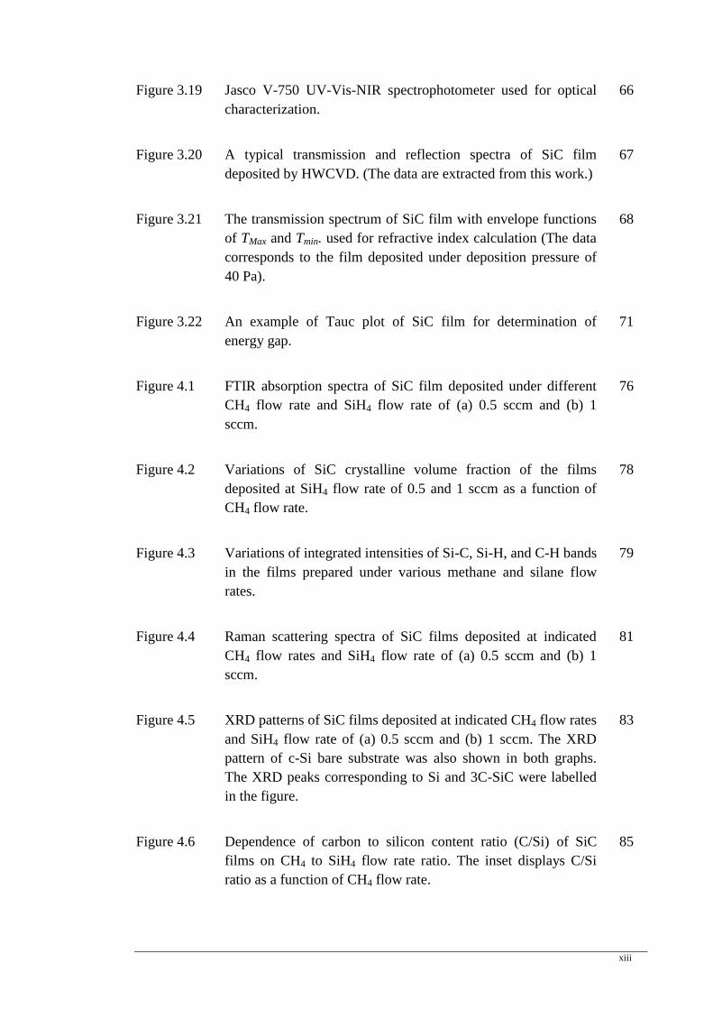
Figure 3.21 The transmission spectrum of SiC film with envelope functions
of TMax and Tmin. used for refractive index calculation (The data
corresponds to the film deposited under deposition pressure of
40 Pa).
68
Figure 3.22 An example of Tauc plot of SiC film for determination of
energy gap.
71
Figure 4.1 FTIR absorption spectra of SiC film deposited under different
CH4 flow rate and SiH4 flow rate of (a) 0.5 sccm and (b) 1
sccm.
76
Figure 4.2 Variations of SiC crystalline volume fraction of the films
deposited at SiH4 flow rate of 0.5 and 1 sccm as a function of
CH4 flow rate.
78
Figure 4.3 Variations of integrated intensities of Si-C, Si-H, and C-H bands
in the films prepared under various methane and silane flow
rates.
79
Figure 4.4 Raman scattering spectra of SiC films deposited at indicated
CH4 flow rates and SiH4 flow rate of (a) 0.5 sccm and (b) 1
sccm.
81
Figure 4.5 XRD patterns of SiC films deposited at indicated CH4 flow rates
and SiH4 flow rate of (a) 0.5 sccm and (b) 1 sccm. The XRD
pattern of c-Si bare substrate was also shown in both graphs.
The XRD peaks corresponding to Si and 3C-SiC were labelled
in the figure.
83
Figure 4.6 Dependence of carbon to silicon content ratio (C/Si) of SiC
films on CH4 to SiH4 flow rate ratio. The inset displays C/Si
ratio as a function of CH4 flow rate.
85
xiv
Figure 4.7 Deposition rate of SiC films deposited at different CH4 flow rate
and SiH4 flow rate of 0.5 and 1 sccm.
87
Figure 4.8 FTIR spectra of the films deposited at different gas partial
pressures with the SiH4 to CH4 flow-rate ratio fixed at 1:20, (a)
The deposition pressure was fixed at the total gas partial
pressure (VP samples) and (b) The deposition pressure was
fixed at 80 Pa (FP samples).
92
Figure 4.9 Raman scattering spectra of (a) VP and (b) FP films. 95
Figure 4.10 Typical deconvolution of Raman spectrum in the ranged of Si-
Si vibrations.
96
Figure 4.11 XRD pattern of SiC films prepared under different total gas
partial pressures (a) VP (b) FP.
98
Figure 4.12 Auger depth profile of SiC films. (a): VP-1, (b): VP-2, (c): VP-
3, (d) VP-4, (e): FP-1, (f): FP-2, (g): FP-3, (h): FP-4.
100
Figure 4.13 Deposition rate of VP and FP films as a function of total gas
partial pressure.
103
Figure 5.1 FTIR spectra of SiC films deposited at different deposition
pressures.
112
Figure 5.2 From top to bottom: integrated intensities of Si-H(str), C-H(w),
and Si-C(str) bonds in SiC films as a function of deposition
pressure.
113
Figure 5.3 Raman scattering spectra with UV excitation (325 nm) from the
SiC films deposited on c-Si substrate under different deposition
pressures.
115
Figure 5.4 Visible Raman spectra of SiC films deposited on c-Si substrate
under various deposition pressures.
116
Figure 5.5 Raman scattering spectra with visible excitation wavelength
from the SiC films deposited under different deposition
pressures in the C-C region.
118
xv
Figure 5.6 Visible Raman scattering spectra of the films deposited under
different deposition pressures on glass substrate.
120
Figure 5.7 XRD patterns of the films deposited under different deposition
pressures on (a) glass and (b) c-Si.
121
Figure 5.8 The variation of relative atomic concentration of silicon, carbon
and oxygen in the films as a function of deposition pressure
obtained from AES analysis.
122
Figure 5.9 Auger depth profile of SiC films deposited under different
deposition pressures.
124
Figure 5.10 FESEM images of the surface of the films deposited at different
deposition pressures.
125
Figure 5.11 (a) UV-Vis-NIR transmission spectra and (b) Absorption
coefficient of the films deposited at different deposition
pressures.
127
Figure 5.12 Dependence of band gap and disorder parameter (B) of SiC
films on the deposition pressures.
129
Figure 5.13 Dependence of band gap of the SiC films prepared under
different deposition pressure on the Si-C bond density of the
films.
130
Figure 5.14 Refractive index of SiC films prepared under different
deposition pressures.
131
Figure 5.15 PL spectra of SiC films deposited under different deposition
pressures.
133
Figure 5.16 Deposition rate of SiC films as a function of deposition
pressure.
135
Figure 5.17 Deposition mechanism of SiC from methane and silane gases in
HWCVD chamber under low and high deposition pressures.
136
xvi
Figure 5.18 FTIR transmission spectra of SiC films deposited under
different filament-to-substrate distances (d).
137
Figure 5.19 Si-C absorption band of SiC films prepared at various filament-
to-substrate distances (d).
138
Figure 5.20 The variations of SiC crystalline volume fraction and Si-C
integrated intensity in the films as a function of d.
139
Figure 5.21 Variation of peak posotion of Lorentzian component of Si-C
band with SiC crystalline volume fraction.
140
Figure 5.22 The IR absorption band in the region of Si-H stretching
vibrations.
141
Figure 5.23 Variations of Si-H and C-H bond densities in the SiC films
versus filament-to-substrate distance.
141
Figure 5.24 Raman scattering spectra of SiC films deposited on c-Si
substrate at indicated d.
143
Figure 5.25 Raman scattering spectra of SiC films deposited at different d in
the range of Si-C vibrations.
143
Figure 5.26 Raman scattering spectra of SiC films deposited at different d in
the range of C-C vibrations.
145
Figure 5.27 Raman scattering spectra of SiC films deposited on glass under
different filament to substrate distance.
146
Figure 5.28 XRD pattern of SiC films deposited under various d on c-Si
substrate. The inset shows variations of SiC crystallite size
estimated from different XRD peaks.
147
Figure 5.29 XRD patterns of SiC films deposited on glass substrate under
various d.
147
Figure 5.30 Auger depth profile of SiC films deposited at different d. 149
xvii
Figure 5.31 Variations of silicon, carbon, and oxygen atomic concentration
versus d.
150
Figure 5.32 FESEM images of the surface of the films deposited at different
filament-to-substrate distances.
151
Figure 5.33 (a) UV-Vis-NIR transmission spectra and (b) Absorption
coefficient of the films deposited at different d.
153
Figure 5.34 Band gap and refractive index of SiC films deposited under
different d.
154
Figure 5.35 Variations of B-parameter, the slope of Tauc plot, and E04-Eg,
the width of band tail as a function of d. The dashed lines are
visual guides.
155
Figure 5.36 Room temperature photoluminescence spectra of the SiC films
deposited under different filament-to-substrate distances.
156
Figure 5.37 Deposition rate of SiC films as a function of d. 158
Figure 5.38 Deposition mechanism in the HWCVD chamber under different
filament-to-substrate distances.
160
Figure 5.39 Variation of energy band gap and refractive index of the SiC
films deposited under different d as a function of G peak
position (top graph) and the integrated intensity of G peak
(bottom graph).
162
Figure 5.40 Energy band gap of SiC films as a function of carbon content in
the films. Full squares show the results obtained in this work.
Other symbols are the values from references for comparison as
indicated in the figure (I. Ferreira et al., 2001; Shen et al., 2012;
B.P. Swain, 2006b; Bibhu P. Swain & Dusane, 2006; A. Tabata,
Kuroda, M., Mori, M., Mizutani, T., Suzuoki, Y., 2004).
163
Figure 5.41 Refractive index of SiC films as a function of carbon content in
the films. Full squares show the results obtained in this work.
Other symbols are the values for PECVD SiC films from
references for comparison as indicated in the figure.
164
xviii
LIST OF TABLES
Page
Table 3.1 Inverse absorption cross sections (A) of various absorption
bands in FTIR spectrum.
53
Table 4.1 Deposition parameters for SiC films used in this chapter. 75
Table 4.2 Si-C and Si-H bond densities of SiC films deposited under
different methane and silane flow rate.
80
Table 4.3 Methane and silane gas flow rates, total gas partial pressure
and deposition pressures in deposition of SiC films in the FP
and VP series.
90
Table 4.4 Relative atomic concentration of constituent elements in SiC
films (set VP and FP) as obtained from Auger depth profile,
and Si-H and Si-C bond densities in the films calculated
from FTIR spectra.
101
Table 5.1 The deposition parameters for the preparation of SiC thin
films at various deposition pressures.
110
Table 5.2 The deposition parameters for the preparation of SiC thin
films at different filament-to-substrate distances.
111
Table 5.3 PL energy and energy band gap of SiC films deposited under
different d.
157
Table A.1 Si-C bond density, deposition rate, and energy gap of the
SiC films deposited by HWCVD technique at various
methane flow rate and two constant silane flow rate.
193
Table A.2 Si-C bond density, deposition rate, and energy gap of the
SiC films deposited by HWCVD technique at various total
gas partial pressures.
194

xix
Table A.3 Si-C bond density, deposition rate, and energy gap of the
SiC films deposited by HWCVD technique at various
deposition pressures.
195
Table A.4 Si-C bond density, deposition rate, and energy gap of the
SiC films deposited by HWCVD technique at various
filament-to-substrate distances.
195

CHAPTER 1: INTRODUCTION
1
CHAPTER 1
Introduction
CHAPTER 1: INTRODUCTION
2
1.1 Introduction
Silicon carbide (SiC) was discovered by an American inventor, Edward G.
Acheson in 1891 while attempting to produce artificial diamonds. It is a wide band gap
semiconductor long known to have potential for high temperature, high power, high
frequency and radiation hardened applications. SiC has been used as an industrial
material since the last century because of its unique properties, such as high thermal
conductivity (3.2 W cm-1
K-1
), high breakdown electric field (2.2 × 10⁶ Vcm
-1), high
forward current density, high saturated electron drift velocity, high electronic mobility,
high blocking voltage, excellent oxidation resistance, strength retention to high
temperature (above 600°C), high wear resistance and so on. The scientific interest in
SiC is driven by the existence of a diversity of different polytypes of SiC. SiC is the
only IV-IV compound that forms stable long-range ordered structures. Over 200
crystallographic modifications of SiC have been reported originating from differences in
the stacking sequence of Si-C double layers along the [111] or [0001] direction. The
most common polytypes of SiC crystals include 3C (zinc blend), 6H, 4H, and 2H
(wurtzite) (Z.C. Feng, 2004; Friedrichs, Kimoto, Ley, & Pensl, 2011; Harris, 1995; Y.
S. Park, 1998).
Hydrogenated amorphous SiC (a-Si1-xCx:H) is also of considerable current
interest both fundamentally, as a typical amorphous system with variable disorder and
microstructure, and technologically, with regard to its applications in electronics and
optoelectronics. Wide applications of this material are due to the fact that its optical gap
can be significantly tailored by varying the compositional ratio of its constituent
elements. In addition, a-SiC:H film is known to be chemically and mechanically
stronger than hydrogenated amorphous silicon (a-Si) films and recently has been
recognized to be compatible for applications in biomedical devices (Saddow, 2012; Will
CHAPTER 1: INTRODUCTION
3
et al., 2010). SiC in its crystalline and amorphous form has also become attractive as an
important wide band-gap semiconductor material for applications in optoelectronic
devices, such as window layer in silicon solar cells (G. Ambrosone et al., 2002; Chang
et al., 2012; Klein, Finger, Carius, & Stutzmann, 2005; Mao et al., 2012; S. Miyajima,
Irikawa, Yamada, & Konagai, 2010; Ogawa et al., 2008). Window layer is a transparent
film that allows full penetration of solar spectrum into the active part of the solar cell.
It is well known that the growth of crystalline SiC thin films requires high
temperatures (above 1000°C) that exceed the melting point of available and cheap
substrates. Therefore, for applications such as in thin film solar cells on cheap glass
substrates, low-temperature deposition of SiC is necessary. Amorphous SiC films can
be easily deposited by glow discharge technique at low substrate temperatures.
Nevertheless, for such applications, a material with high electron mobility is desired.
Later studies showed that nano-crystalline SiC, which contains SiC nano-crystallites
embedded in an amorphous SiC matrix, is more suitable than amorphous SiC for
applications in solar cells. Many researchers have attempted to produce this kind of SiC
thin films, which is expected to exhibit excellent properties due to the quantum
confinement effect (Chang, et al., 2012; Q. Cheng, Xu, S. , 2007; Y. Hoshide, Tabata,
A., Kitagawa, A., Kondo, A., 2009; Jha et al., 2012; A. Tabata, Komura, Hoshide,
Narita, & Kondo, 2008).
Amorphous and nanocrystalline SiC thin films have been conventionally grown
by plasma enhanced chemical vapour deposition (PECVD) technique, which allows low
substrate temperature growth at temperatures below 300°C. However, it has some
disadvantages such as low deposition rate and degradation of SiC optical properties
induced by the surface damage due to ion bombardment effect.
CHAPTER 1: INTRODUCTION
4
Hot-wire chemical vapour deposition (HWCVD) technique, invented for
deposition of Si films at high deposition rate, has been realized to be a promising
method to grow high quality SiC films at low substrate temperature compared to those
prepared by conventional PECVD method (A. A. Kumbhar, Dusane, Bauer, &
Schröder, 1998; A. S. Kumbhar, Bhusari, & Kshirsagar, 1995; Mahan, Nelson,
Salamon, & Crandall, 1991). The presence of neutral radicals and molecules instead of
ionized plasma in this system during the growth process makes it a more attractive
process for thin film growth. This technique involves an efficient decomposition of the
source gas catalytically in the presence of a resistively heated filament (usually
tungsten). The generated species are transported to the substrate for film growth at low
temperatures in the range of 150°C – 400
°C, making the process suitable for film growth
on low-cost glass substrates. Also, a HWCVD system is simple to develop and can be
built in any research laboratory at low-cost without complications. This technique
emphasizes gentle reactions on the growing surface and is free from ion bombardment
damage. The deposition area could be expanded arbitrarily by enlarging the spanning
area of the catalyser filaments. In HWCVD, the gas utilization efficiency is 5 to 10
times higher than in PECVD, thus contributing to higher growth rate of the material.
The HWCVD thus provides enormous promise for better technological feasibility in the
commercial production of large area semiconductor devices (Chakraborty & Das, 2006;
Matsumura, Umemoto, Izumi, & Masuda, 2003). Therefore, there has been a growing
interest in the last decade among researchers to produce SiC films for optoelectronic
applications using HWCVD technique. It has been generally accepted that HWCVD
generates H radicals at a higher density than plasma processes by 1 or 2 order of
magnitude (Umemoto, 2002). It is commonly believed that H radicals play an important
role in the low-temperature growth of nanocrystalline Si-based thin films (Matsuda,
2004). Thus, for deposition of nanocrystalline SiC films, usually the source gases are
CHAPTER 1: INTRODUCTION
5
diluted by hydrogen gas. However, this significantly reduces the growth rate of the
films, which is a disadvantage from the view point of cost reduction. In addition, it
should be noted that a PECVD system is comparatively more expensive and less
economical to run than a HWCVD system. A home-built HWCVD system has the
added advantage of flexibility for design modification to suit the needs of research for
enhancing the properties of the films produced for relevant applications.
In spite of the abundance of published works on the deposition of silicon films
by HWCVD with detailed investigations on its optical and structural properties, similar
research aspects done on SiC films are still lacking. Many aspects on the growth
mechanism of SiC films by HWCVD technique particularly and studies on the
dependence of its properties on the deposition conditions have yet to be understood.
In this work, a home-built HWCVD system in the Low Dimensional Materials
Research Centre (LDMRC), University of Malaya was utilized to grow SiC thin films.
This system was designed and built by Aniszawati Azis, a former PhD student in the
centre for her PhD research. She has shown in her work that this system has the ability
to produce SiC films (Azis, 2012). However, the films were mostly Si-rich and
amorphous and the density of Si-C bonds in the films was low. Moreover, very little
investigation was done on the properties of the films deposited using this system since
the focus of her research was mainly to design and build the HWCVD system and to test
it for the production of SiC films. In the present work, this system has been slightly
modified to improve the efficiency of the system and selected deposition parameters
have been chosen as the variable parameters studied to be optimized for production of
good quality SiC films. Various important characterization techniques will be utilized to
study the films’ properties with respect to the deposition parameters. In addition, the
growth mechanism of SiC films produced by this system will be studied from analysis
CHAPTER 1: INTRODUCTION
6
done on the structural properties of the films with respect to the deposition parameters
studied.
Some neglected aspects of SiC films deposited by HWCVD, specifically from
pure silane and methane gases without hydrogen dilution will be explored in this work.
The deposition parameters are known to significantly influence the growth mechanism
and the film properties. However, investigations on the effect of some important
deposition parameters on the film properties is still needed to understand the growth
mechanism of the films by HWCVD, especially in the absence of hydrogen dilution
which has been established to be necessary to produce nano-crystalline SiC films. The
effect of deposition parameters such as filament-to-substrate distance, methane gas
flow-rate and total gas partial pressure on the SiC deposition mechanism and film
properties have occasionally been reported (A. Tabata & Komura, 2007) but more
studies are still needed to fully justify the reported effects. Also, studies on the
correlation of the structural properties with respect to the important optical parameters
like optical energy gap and refractive index of SiC films have not been reported much in
literature. In this work, the above mentioned issues will be investigated
comprehensively.
1.2 Objectives of Research
In order to address the issues much needed to understand the properties and
deposition mechanisms of SiC films grown by HWCVD as mentioned above, this PhD
thesis will present the work done to achieve the following objectives:
1. To produce SiC film involving high Si-C bond density with wide-band gap
using a home-built HWCVD system at high deposition rate from a mixture of
pure silane and methane gases without hydrogen dilution.
CHAPTER 1: INTRODUCTION
7
2. To determine the influence of critical deposition parameters on the structural and
optical properties of SiC films deposited. The important deposition parameters
include methane gas flow-rate, total gas partial pressure, deposition pressure and
filament-to-substrate distance.
3. To determine that the structural properties of SiC films are not dependent on the
substrate used and correlate the structural properties to the optical properties of
the films.
4. To determine the growth mechanisms of these SiC thin films grown by
HWCVD technique from the discharge of pure silane (SiH4) and methane (CH4)
without hydrogen dilution.
In order to achieve these main objectives, the results in this work are presented,
discussed and analyzed in two main chapters with specific objectives detailed in each of
these chapters.
1.3 Organization of the Thesis
This thesis is organized into six chapters. Chapter 2 provides a brief literature
review related to this research. This chapter provides some information on SiC material
and its various structures, properties and applications. Subsequently, description on the
HWCVD technique is provided with information on the advantages of this technique
and its development in the deposition of SiC.
Chapter 3 presents the experimental and analytical methods involved in this
research. This chapter consists of two main parts and the first part includes a description
of the home-built HWCVD deposition system and all the procedures required for
deposition of SiC film including substrate cleaning, filament pre-heating and the film
CHAPTER 1: INTRODUCTION
8
deposition procedures. The second part of this chapter presents various characterization
techniques utilized in this work. This part gives a description of each characterization
method, instrumentation and theoretical calculation involved.
The results and discussions are presented in Chapters 4 and 5. Chapter 4 presents
the study on the effects of methane gas flow-rate at silane starving condition and the
total gas partial pressure on the crystallinity, elemental composition and chemical
bonding properties of films grown on crystal silicon substrates. Chapter 5 presents the
study on the influence of deposition pressure and filament-to-substrate distance, two
important deposition parameters in HWCVD on the structural, elemental composition,
morphology and optical properties of films deposited on both glass and crystal silicon
substrates. Correlation between the structural and optical properties of the films is
presented and discussed in this chapter. Finally, the growth mechanisms of SiC films
are formulated and presented based on the all the results obtained. This thesis is
concluded in Chapter 6 along with suggestions for future works on the SiC films
deposited using the home-built HWCVD system.

CHAPTER 2: LITERATURE REVIEW
9
CHAPTER 2
Literature Review
CHAPTER 2: LITERATURE REVIEW
10
2.1 Introduction
This chapter presents a literature review related to this research, which contains
three parts. The first part provides general information about silicon carbide material, its
structural properties and potential applications. The second part involves most
conventional deposition techniques used for preparation of SiC thin films and their
advantages and disadvantages. The last part of this chapter will introduce hot-wire
chemical vapour deposition as a technique used in this work and give a brief history of
its development, its advantages over other techniques, and some proposed chemical
reactions involved during the deposition process.
2.2 General Properties of Silicon Carbide
Silicon carbide (SiC) is a binary compound, which is well known as an
important wide band gap semiconductor. It is the only chemically stable form of Si and
C atoms. Since Si and C are both group IV atoms, they are covalently bonded.
Nevertheless, because of the difference in electronegativity of Si and C, this compound
has 12% ionicity (Yoshida et al., 2007).
SiC is a part of a family of materials called polytypism that is a one-dimensional
polymorphism. An almost infinite number of SiC polytypes are possible, and
approximately 250 polytypes have been already discovered (Fissel, 2003; Karch,
Bechstedt, Pavone, & Strauch, 1996; Wang, Ma, & Zupan, 2006; Willander, Friesel,
Wahab, & Straumal, 2006). Different polytypes arise from the different stacking
sequences of the Si-C bilayer producing crystals with different unit cell dimensions
along the [0001] or c-axis. The reason for the stability of so many polytypes in SiC is
not well understood yet. It is noticeable that each polytypes differs from the others in
CHAPTER 2: LITERATURE REVIEW
11
terms of band gap, and other fundamental properties. Therefore, SiC can be considered
as a family of a large number of semiconductors. The most dominant polytypes are 3C
(cubic), 2H, 4H and 6H (hexagonal), and 15 R (rhombohedral). The number represents
the number of double layers in the stacking sequence and the letter represents crystal
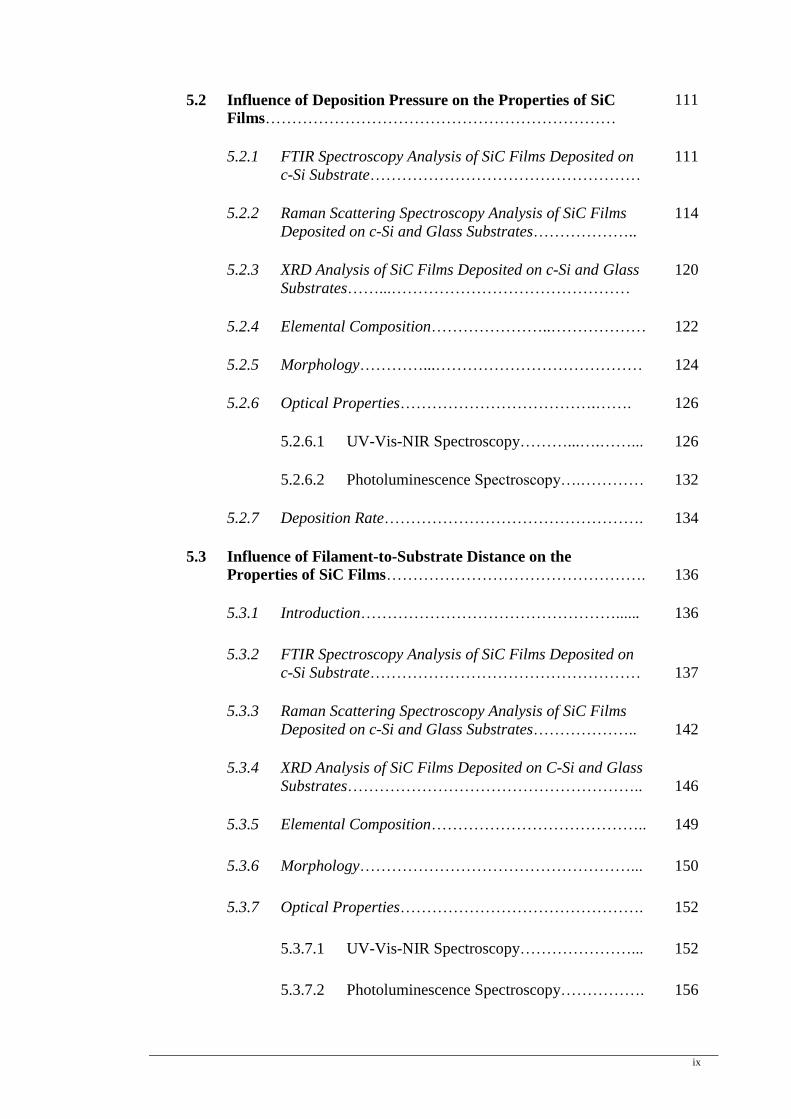
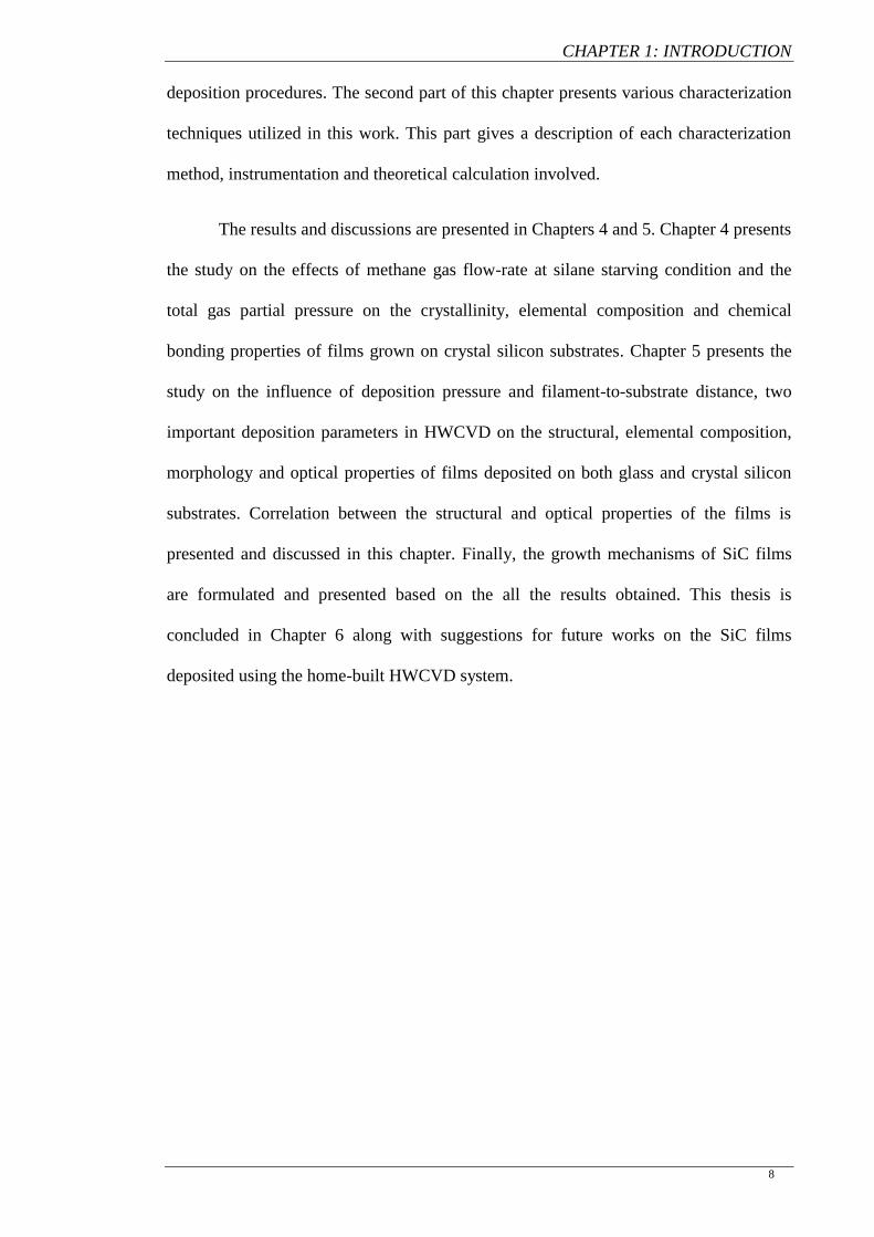
structure. Figure 2.1 illustrates the three most common SiC polytypes.
Figure 2.1: The three most common polytypes in SiC viewed in the [1120] plane. From left to
right, 4H-SiC, 6H-SiC, and 3C-SiC; k and h denote crystal symmetry points that are cubic and
hexagonal, respectively.
It is well known that among the different SiC polytypes, the cubic SiC (3C-SiC)
exhibits the highest electron mobility and is more stable than hexagonal system.
Meanwhile, it is the only one that can be grown on low-cost Si substrates to merge into
the well-developed Si-bases integration technology (Zhe Chuan Feng, 2006; Hiromasa,
Takahiro, Tetsuya, Hiroaki, & Kiyoshi, 2011; Komiyama, Abe, Suzuki, Kita, &
Nakanishi, 2005).
Physical properties of crystalline SiC, such as high thermal conductivity, high-
saturated drift velocity, and high breakdown field make it attractive for many
CHAPTER 2: LITERATURE REVIEW
12
applications including high temperature, high power and high frequency devices that are
not possible using Si or GaAs. SiC is also resistant to high radiation doses and thus
suitable for nuclear power applications (Harris, 1995; Y. S. Park, 1998). However,
because of difficulties in production of good quality SiC single crystals with low cost,
the SiC technology has faced major limitation yet.
Beside crystalline SiC, its amorphous form (a-SiC) has attracted much attention
due to its magnificent properties such as high stability, tuneable band gap and refractive
index by varying the chemical composition and so on. Si-rich a-SiC is usually employed
as a transparent layer in solar cells and photo-detectors, while C-rich a-SiC films are a
good candidate as an active layer in electroluminescent devices (Q. Cheng & et al.,
2008; Vasin, 2008). In addition, due to coexistence of topological, structural and
compositional disorder, it is a representative material for fundamental studies of an
amorphous system with variable disorder (Compagnini, Foti, & Makhtari, 1998; El
Khakani, Guay, Chaker, & Feng, 1995; Rovira & Alvarez, 1997; Solomon, 2001;
Tersoff, 1994). This complexity of a-SiC films has led to long time study on this
material which has been deposited by various deposition techniques.
It should be mentioned that there are other structures than crystalline and
amorphous SiC that have been obtained by several researchers that are microcrystalline
and nano-crystalline SiC. These structures involve crystalline SiC or Si grains that
embedded in the amorphous SiC matrix. These kinds of systems usually exhibit unique
and interesting properties such as strong room temperature PL, wide band gap and high
electron mobility as reported in the literature (G. Ambrosone et al., 2006; Coscia,
Ambrosone, & Basa, 2008; Klein, Dasgupta, Finger, Carius, & Bronger, 2008; Xu, Yu,
Rusli, Yoon, & Che, 2000; M. B. Yu, Rusli, Yoon, Xu, et al., 2000; W. Yu, Wang, X.,
Lu, W., Wang, S., Bian, Y., Fu, G., 2010). It should be mentioned that these unique
properties have been attributed to the quantum confinement of nano-crystallites.
CHAPTER 2: LITERATURE REVIEW
13
The structural model of amorphous and nano-crystalline SiC is not unique. This
is because of the capability of carbon to have twofold, threefold and fourfold
coordination adds a degree of freedom in local structure arrangement which is absent in
the other amorphous semiconductor alloys. However, there have been some suggested
models of chemical ordering in amorphous silicon carbon alloys according to what have
been obtained from various theoretical and experimental techniques. (Bhusari &
Kshirsagar, 1993; King, et al., 2011; Lee & Bent, 2000; Pascarelli, Boscherini, Mobilio,
& Evangelisti, 1992; Rovira & Alvarez, 1997; Tersoff, 1994). Here, some of these
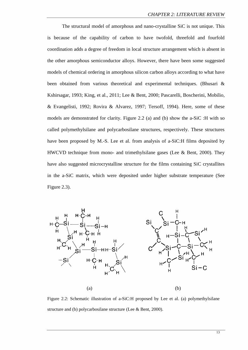
models are demonstrated for clarity. Figure 2.2 (a) and (b) show the a-SiC :H with so
called polymethylsilane and polycarbosilane structures, respectively. These structures
have been proposed by M.-S. Lee et al. from analysis of a-SiC:H films deposited by
HWCVD technique from mono- and trimethylsilane gases (Lee & Bent, 2000). They
have also suggested microcrystalline structure for the films containing SiC crystallites
in the a-SiC matrix, which were deposited under higher substrate temperature (See
Figure 2.3).
(a) (b)
Figure 2.2: Schematic illustration of a-SiC:H proposed by Lee et al. (a) polymethylsilane
structure and (b) polycarbosilane structure (Lee & Bent, 2000).
CHAPTER 2: LITERATURE REVIEW
14
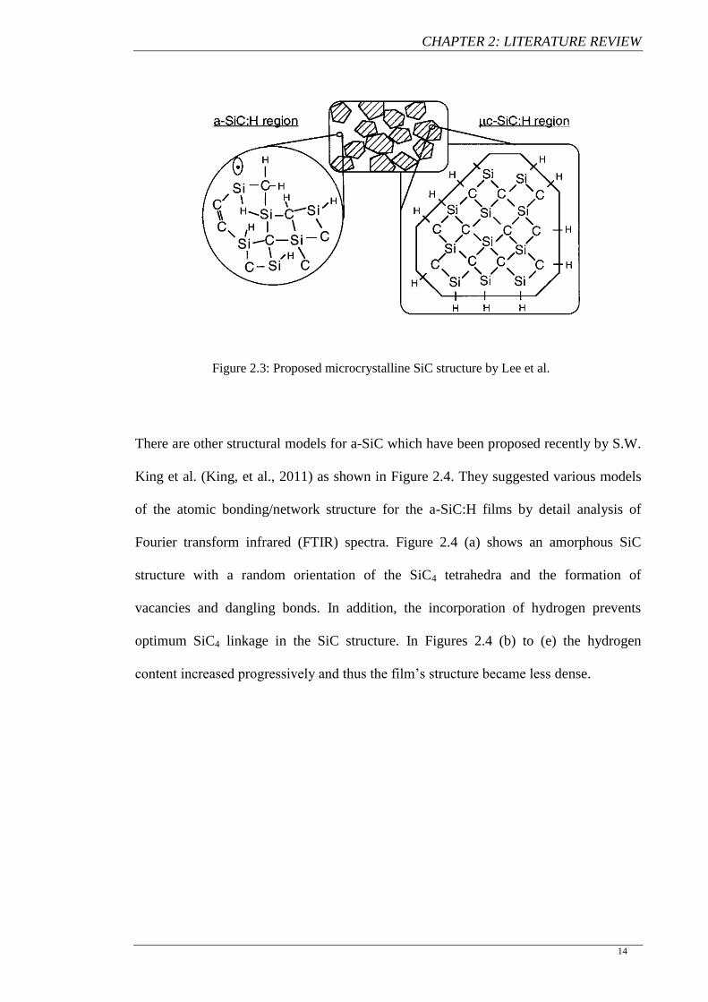
Figure 2.3: Proposed microcrystalline SiC structure by Lee et al.
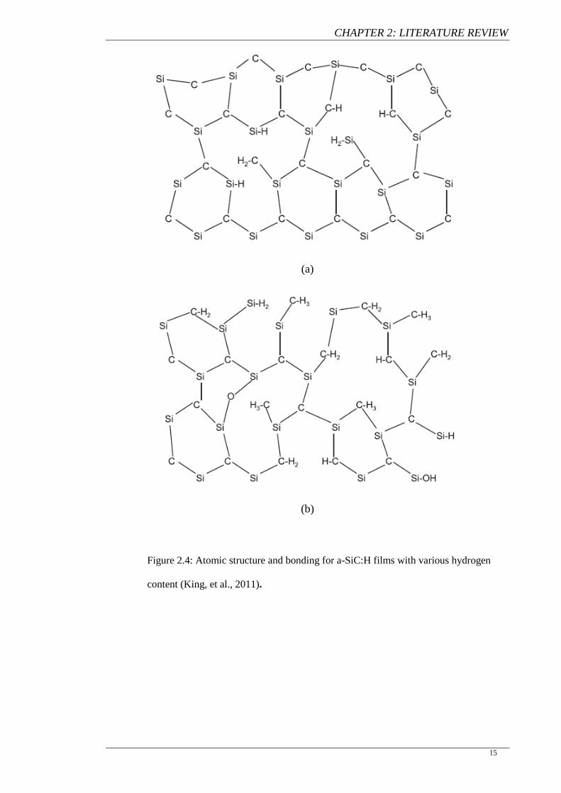
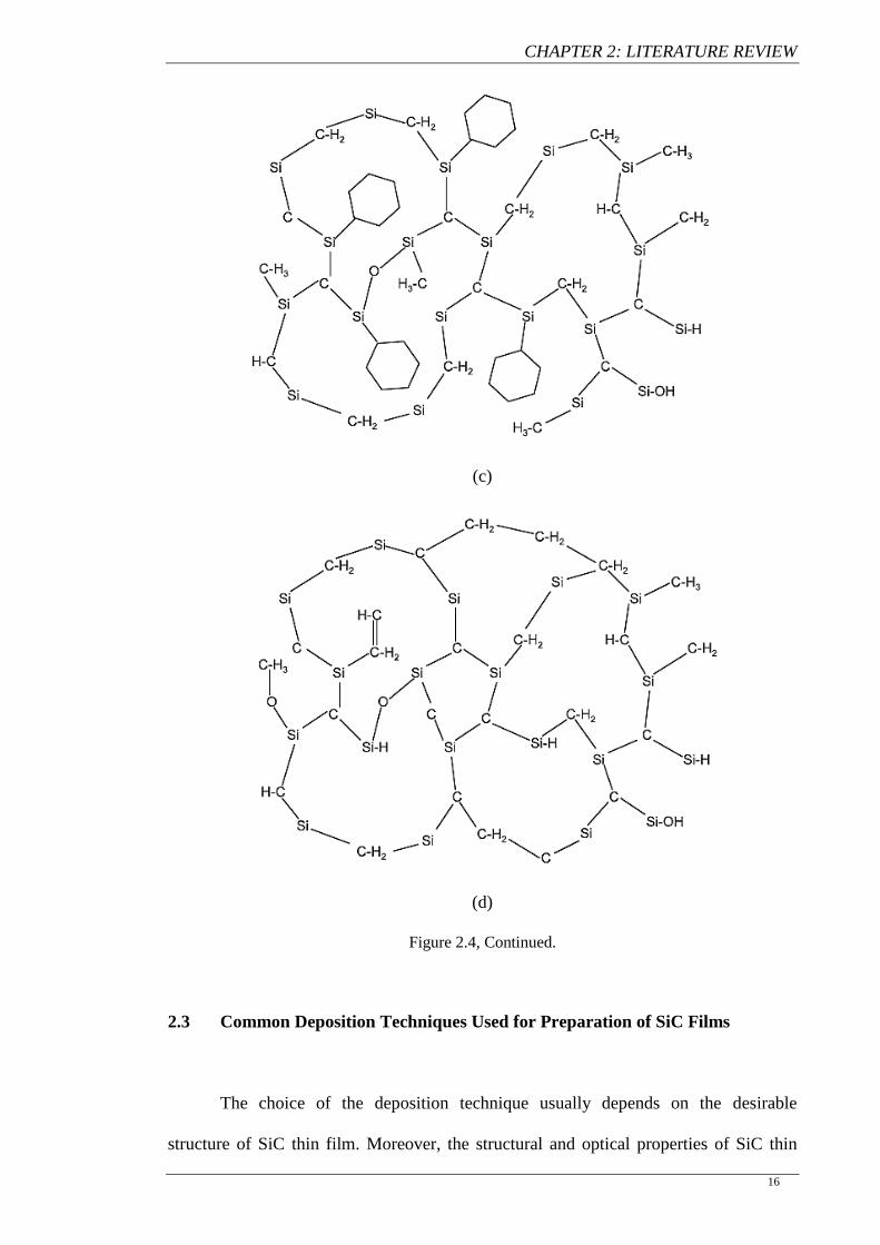
There are other structural models for a-SiC which have been proposed recently by S.W.
King et al. (King, et al., 2011) as shown in Figure 2.4. They suggested various models
of the atomic bonding/network structure for the a-SiC:H films by detail analysis of
Fourier transform infrared (FTIR) spectra. Figure 2.4 (a) shows an amorphous SiC
structure with a random orientation of the SiC4 tetrahedra and the formation of
vacancies and dangling bonds. In addition, the incorporation of hydrogen prevents
optimum SiC4 linkage in the SiC structure. In Figures 2.4 (b) to (e) the hydrogen
content increased progressively and thus the film’s structure became less dense.
CHAPTER 2: LITERATURE REVIEW
15
(a)
(b)
Figure 2.4: Atomic structure and bonding for a-SiC:H films with various hydrogen
content (King, et al., 2011).
CHAPTER 2: LITERATURE REVIEW
16
(c)
(d)
Figure 2.4, Continued.
2.3 Common Deposition Techniques Used for Preparation of SiC Films
The choice of the deposition technique usually depends on the desirable
structure of SiC thin film. Moreover, the structural and optical properties of SiC thin
CHAPTER 2: LITERATURE REVIEW
17
films strongly depend on deposition technique as well as deposition conditions. In this
section, a preview of conventional deposition techniques for preparation of SiC films
and highlighted properties of resulting films will be presented.
Based on the literature, two main groups of deposition techniques have been
conventionally adopted for preparation of SiC thin films; chemical vapour deposition
(CVD) and sputtering. It should be noted that each of them involves several sub-
methods in terms of supplied activation source. However, beside these most widely used
techniques, other deposition techniques have been also reported for preparation of SiC
thin films such as Laser assisted deposition (LAD) (Sung et al., 1992), ion beam
assisted deposition (Rivière, Zaytouni, & Delafond, 1996) and sublimation (Oulachgar,
Aktik, Dostie, Gujrathi, & Scarlete, 2007). Nevertheless, this section will only
concentrate on the mentioned main conventional techniques based on the literature.
2.3.1 Chemical Vapour Deposition (CVD) Methods
For deposition of SiC films in the forms of single and polycrystalline SiC and
amorphous, chemical vapour deposition technique has been widely employed (Dhanaraj
et al., 2007; Ellison et al., 2000; Ellison et al., 1999; Kordina et al., 1996; Morgan,
2006; Y. S. Park, 1998). In a typical chemical vapour deposition process the substrate is
exposed to one or more unstable precursors, which react with the substrate surface to
yield the desired deposit (Comninellis & Chen, 2009). In this process, the activation
energy for chemical reactions can be supplied by various energy sources. If heating the
substrate is used to activate the reaction of precursors, the process is called thermal
CVD. For this purpose, usually high temperature above 1000°C is required. As a result,
uniform and reproducible films are grown. However, the main limitation of this
CHAPTER 2: LITERATURE REVIEW
18
technique is its required high temperature, which suffers from structural damage and
formation of voids in the films (S. H. Feng & Chen, 2002).
Photo-assisted CVD is an alternative modification of CVD method, which has
been used for amorphous and nano-crystalline SiC deposition (Chevaleevski, Myong, &
Lim, 2003; Dasgupta, Ghosh, Kshirsagar, & Ray, 1997; Lim & Shevaleevskiy, 2008;
Yeop Myong, Kew Lee, Yoon, & Su Lim, 2002). There are two main variants of this
method as light source of excitation used in the decomposition process:
(i) Laser-induced Photo-CVD, which uses high-energy coherent radiations
as light source to decompose reactive gases. In this manner, various gas
lasers can be used. However, they are expensive while some effects such
as damage due to high-energy photons are expected.
(ii) Lamp-induced Photo-CVD, which uses incoherent radiations to perform
an indirect photolysis mechanism. Usually a low-pressure Hg lamp is
used to dissociate the gas mixture due to high catalytic activity of
mercury. It is a soft process because the damage of the film surface by
the ions is negligible. Therefore, less bombardment-induced defects and
sharper interfaces are expected especially in very thin films (Bullot &
Schmidt, 1987).
Plasma-enhanced CVD (PECVD) is a modification of CVD method and
undoubtedly has been the most conventional deposition technique for production of SiC
films. In this method, plasma is used as a source of energy in order to dissociate the
reactive gases at temperatures much lower than their pyrolysis temperature. Plasma can
be defined as a gas vapour in which a part of the atoms (molecules) has been ionized.
The main advantage of this method is its low operation temperature, which is usually
below 400°C. Moreover, this method has ability to deposit films on various substrates
CHAPTER 2: LITERATURE REVIEW
19
over a large area (Hori & Goto, 2002). However, decrease in optical gap for high carbon
content SiC films have been observed due to graphite like sp2 C-C bonding (Hu, 2004).
In addition, presence of large density of ions in the plasma sometimes causes surface
damages due to ion bombardment. It is worth noting that for deposition of
nanocrystalline silicon carbide films, heavy hydrogen dilution is necessary that
significantly decreases the deposition rate.
Next modification of CVD method is electron cyclotron resonance CVD (ECR-
CVD) that have been used for deposition of amorphous and crystalline SiC films
(Chew, 2002; Conde et al., 1999; Toal, Reehal, Barradas, & Jeynes, 1999; Xu, et al.,
2000). The principle of this technique is that the frequency of the input source (usually
in the microwave region) is matched with the cyclotron frequency set by magnetic field
in a resonant chamber. When this matching occurs, electrons adsorb energy from the
exiting electric field. Since in ECR-CVD the ion energy is low, the energy of impinging
ions on the surface can be controlled independently of the microwave power by
applying a bias voltage to the substrate electrode. In addition ECR plasma is usually
operated at low pressures (< 10 mTorr) which avoids polymerization by reducing the
number of gas-phase collisions and allow sharper interfaces (Conde, et al., 1999).
Catalytic CVD (also known as hot wire or hot filament CVD) is another simple
modification of CVD technique, which is conventionally employed to produce Si-based
and diamond films (Mahan, 2003; Mahan, Carapella, Nelson, Crandall, & Balberg,
1991; Martin, Teplin, Doyle, Branz, & Stradins, 2010; Matsumura, 1998; Soni, Phatak,
& Dusane, 2010). This technique has become attractive in last two decades for
deposition of device quality amorphous and nano-crystalline Si films at high deposition
rate. Many research works have been published on both better understanding of this
technique and toward optoelectronic applications especially in solar cells. However,
much less references are available in the literature about the deposition of SiC thin films
CHAPTER 2: LITERATURE REVIEW
20
by this technique. Since this technique is the subject of the present study, it will be
described in more details in section 2.4.
2.3.2 Sputtering Methods
Cathodic sputtering is a multipurpose thin film deposition method used for a
long time in different industrial developments. The principle of sputtering is that a solid
is subjected to bombardment by high-energy particles such as ions. As a result,
individual atoms or molecules achieve enough energy to escape from the surface. These
ejected atoms or molecules can then form a new layer on the substrate surface. The
sputter deposition is generally a more physical than chemical process. Physical
sputtering of polycrystalline SiC target by argon ions always yields unhydrogenated and
nearly stoichiometric materials. Co-sputtering from silicon and graphite targets allows
variable Si/C ratio of the films. Sputtering in the presence of reactive gases such as H2,
CH4 and SiH4 leads to incorporation of desirable amount of hydrogen as well as Si/C
ratio into the films (Bullot & Schmidt, 1987). Therefore, by this method it is possible to
avoid use of toxic gases as well as accurately control the film thickness.
Deposition of various structures of SiC film by sputtering technique has been
reported. Nano-crystalline SiC has been prepared by co-sputtering of silicon and carbon
targets in H2 environment (Kerdiles, 2000; Kerdiles, Madelon, & Rizk, 2001).
Amorphous hydrogenated SiC films have been deposited by d.c. sputtering of
polycrystalline Si target in the presence of CH4 and H2 gases as source of C and H in the
film (Saleh, Munisa, & Beyer, 2003). Unhydrogenated amorphous SiC films have been
obtained by sputtering of SiC target in the presence of Ar gas (Seo, Joung, Park, &
Choi, 2011; Tang, Tan, Huang, Dong, & Jiang, 2005).
CHAPTER 2: LITERATURE REVIEW
21
2.4 Hot-Wire Chemical Vapour Deposition (HWCVD) Technique
2.4.1 History of HWCVD Technique
Hot-wire chemical vapour deposition (HWCVD) technique was first introduced
in 1979 by Weismann et al (Wiesmann, Ghosh, McMahon, & Strongin, 1979). They
could deposit amorphous hydrogenated silicon (a-Si:H) thin films by high-temperature
thermal decomposition of silane using a heated tungsten filament with relatively high
deposition rate. However, their films were poor in quality due to low pressure they used
in the deposition process. Therefore, researches on this method remained stagnated until
1988 that Matsumura et al (Matsumura & Ihara, 1988) obtained good quality a-Si:H
films with high deposition rate by using much higher pressures. Since they discover the
catalytic role of the heated filament in decomposition of SiH4 molecules, they named it
as “Catalytic-CVD (Cat-CVD)” method. Device quality a-Si:H films deposited by the
same method with hydrogen content as low as 1%, which is desired for solar cell
applications, was reported in 1991 by Mahan et al (Mahan, Carapella, et al., 1991;
Mahan, Nelson, et al., 1991). This research group, however, called this deposition
technique as “HWCVD”. Since then, HWCVD has attracted much interest as a
promising deposition technique for Si-based materials thin films.
2.4.2 Advantages of HWCVD
The highlighted advantages of HWCVD method and resulting Si-based thin
films are listed below (Feenstra, Schropp, & Van der Weg, 1999; Gogoi, Jha, &
Agarwal, 2010; Matsumura, 1998; Soni, et al., 2010):
CHAPTER 2: LITERATURE REVIEW
22
i. High deposition rate: For deposition of Si-based thin films high deposition
rates > 10 Å/s can be achieved without the deteriorating their device quality.
This value is an order of magnitude higher than that expected using PECVD
methods (Feenstra, et al., 1999; Takashi Itoh et al., 2001; Jadkar et al., 2007;
Jadkar, Sali, Musale, Kshirsagar, & Takwale, 2002; Matsumura, Umemoto, &
Masuda, 2004).
ii. Ion-free plasma: In HWCVD technique, only neutral atoms and molecules
(radicals) are present in the gas phase. Therefore, the film surface does not suffer
from plasma damage or charge-induced damage. This makes HWCVD a
“gentle” process (Mahan, 2003; Matsumura, et al., 2004).
iii. Easily scalable deposition system: An extreme simplicity of geometry of the
HWCVD system allows one to control the deposition process easily by adjusting
only few parameters.
iv. Low cost of HWCVD system
v. Large area deposition: The deposition area can be easily widened by expansion
of the spanned area of filaments.
vi. Low substrate temperature: The substrate temperature in HWCVD method is
usually set to 300°C or less. Meanwhile, the radiations from the hot filament
does not significantly effect on the substrate temperature when the distance
between filament and the substrate is above 10 mm. Low-temperature deposition
techniques are desired from the viewpoint of widening the application of SiC
films in optoelectronic devices such as solar cells and thin film transistors.
Moreover, for such applications, SiC film must be deposited on glass substrates
that require low-temperature deposition method.
vii. Lower hydrogen incorporation into the film: To saturate dangling bonds in a-
Si:H, theoretically about 0.1% hydrogen alloying is required. Materials
CHAPTER 2: LITERATURE REVIEW
23
deposited by HWCVD show significant lower hydrogen content (about 1%)
compared to those of deposited by PECVD (above 10%). Therefore, it is
expected that low-hydrogen Si-alloys prepared using HWCVD are superior for
optoelectronic applications (Mahan, 2003).
viii. High efficiency gas usage: It is generally accepted that for the filament
temperatures above 1800 °C, SiH4 gas completely decompose into Si and H
atoms. This high efficiency gas decomposition significantly reduces the
deposition cost.
2.4.3 Some Physics and Chemistry of HWCVD
Since the invention of HWCVD technique, several research groups have studied
the chemical reactions and kinetics in this method both experimentally and theoretically
(Doyle, Robertson, Lin, He, & Gallagher, 1988; Duan, Zaharias, & Bent, 2002;
Gallagher, 2001; Holt et al., 2001; Mahan, Carapella, et al., 1991; Matsumura & Ihara,
1988; Umemoto, 2002; van Veenendaal & Schropp, 2002; Zheng & Gallagher, 2006).
These studies mostly have performed in Si deposition in the form of amorphous, poly-,
micro, and nano- crystalline structures. Therefore, currently extensive works are
available about the chemical reactions of different radicals produced in the HWCVD
system. In this section, a brief explanation of what occur in Si deposition by HWCVD is
presented.
The deposition process in the HWCVD system is generally composed of three
stages:
i. Catalytically dissociation of source gases on a resistively heated filament
surface,
ii. Gas phase reactions in the region between filament and the substrate, and
CHAPTER 2: LITERATURE REVIEW
24
iii. Surface reactions on the substrate and growing surface that is heated by
an external heater or by the radiations from the hot filament itself.
It has been established that a tungsten filament with a temperature of 1400ºC and
above is able to decompose silane (SiH4) gas, which is usually utilized in Si deposition.
However, filament temperature above 1800°C is advantageous since it avoids
incorporation of Si atoms into and onto the filament surface i.e. silicide formation on the
filament surface and hence shortening the filament lifetime due to breakage.
Meanwhile, higher filament temperature (>1800 ºC) leads to efficient decomposition of
silane gas into atomic silicon and hydrogen as shown in following reaction (Gallagher,
2001; Jadkar, et al., 2002; van Veenendaal & Schropp, 2002):
SiH4 Si + 4H (2.1)
Heintze et al. discovered that Si film could not be deposited when the W wire is
covered with Al2O3, even if its temperature exceeds 1600°C. They concluded that the
reaction at the hot filament is catalytic (Heintze, Zedlitz, Wanka, & Schubert, 1996).
The catalytic role of the filament in this cracking reaction has been also proven by
several investigations (Duan, et al., 2002; van Veenendaal & Schropp, 2002). They have
shown that the decomposition probability is dependent on both filament material and
temperature. Moreover, the small activation energy of silane decomposition strongly
confirms that the cracking reaction of silane is catalytic rather than thermal (Duan &
Bent, 2005; Mahan, 2003). The activation energy for pyrolytically cleave four Si-H
bonds in SiH4 is 12.9 eV, while decomposition of SiH4 by a hot tungsten filament only
needs 0.74 eV energy (Mahan, 2003).
Hot filament (>1800 °C)
CHAPTER 2: LITERATURE REVIEW
25
Beside the generation of radicals, the transport of the radicals from the filament
to the substrate surface has a critical influence on the film properties. The deposition
pressure and the distance between the filament and the substrate influence the reactions
on the path from the filament to the substrate. If the deposition pressure is too low in
such a way that the mean free path of Si and H atoms emitted from the hot filament is
equal or greater than the distance between filament and the substrate, they will reach
and diffuse into the substrate without any further reactions. Otherwise, they will go
through a chain of subsequent gas-phase reactions with the existing molecules and
radicals in the chamber before reaching the growth surface. These reactions determine
the growth species for the film deposition. It should be mentioned that the stability,
sticking coefficient and surface mobility of the generated species are important for the
film growth.
The gas phase reactions involve radical-molecule and radical-radical reactions.
i. Radical-molecule reactions
The insertion reaction of Si into silane and the abstraction reaction of hydrogen
are the most important reactions in the gas phase. The insertion reaction of Si can be
done in two possible forms as follows:
Si + SiH4 → SiH +SiH3 (2.2)
Si + SiH4 → HSiSiH3 (2.3)
However, the later reaction is energetically more favourable because it is an
exothermic reaction. It should be noted that HSiSiH3 compound is not stable and will be
stabilized via reactions (Mahan, 2003; Muller, Holt, Goodwin, & Goddard, 2000; van
Veenendaal & Schropp, 2002):
CHAPTER 2: LITERATURE REVIEW
26
HSiSiH3 → H2SiSiH2 (2.4)
or further reacts with SiH4 :
HSiSiH3 +SiH4 → SiH2 + Si2H6 (2.5)
The abstraction reaction of hydrogen has been proposed as follows:
H + SiH4 →SiH3 +H2. (2.6)
It is generally accepted that SiH3 is quite stable species and will not go through further
gas phase reactions. Thus, it is a primary source of the film growth.
ii. Radical-radical reactions
The next gas phase reactions involve radical-radical collisions. Some of possible
radical-radical reactions are:
H + SiH3 →SiH2 + H2 (2.7)
H + Si2H2 → Si2H + H2 (2.8)
SiH3 + SiH3 → SiH4 +H2 (2.9)
These reactions become important at higher pressures due to increment of
radical density in the chamber. Usually, generation of the above products as a result of
radical-radical interactions has negative effects on the structural and optical properties
of the film.
Reactive species, impinging onto a surface can react at the surface to form new
species, which are adsorbed onto the substrate surface. The deposition rate of the film is
CHAPTER 2: LITERATURE REVIEW
27
determined by the flux of radicals impinging on the substrate and the reaction
probability with the film surface. Although the gas phase chemistry of HWCVD is
believed to be very different compared to the conventional thermal CVD and PECVD,
however, the it has been proposed that the deposition models used in PECVD and
HWCVD should be similar (Gallagher, 2001; van Veenendaal & Schropp, 2002).
Surface reactions generally involve (Pant, Russell, Huff, Aparicio, & Birkmire, 2001):
i. Adsorption of radicals and film precursors on the film surface,
ii. Surface rearrangement reactions.
Atomic Si, SiH, and SiH2 have much higher surface reaction rate than SiH3
because the former radicals can directly insert in SiH bond of the surface while SiH3
requires a surface dangling bond. This is commonly described by a value called the
sticking probability (s). Theoretical and empirical values of the sticking probability of
SiHx molecules have been reported for PECVD and HWCVD systems. The sticking
probability of SiHx (x=0-4) has been shown to depend inversely on the number of H atoms
bonded to Si in the growth radical (Pant, Huff, & Russell, 2001). However, I.T. Martin
et al. have shown that the sticking coefficient of the growth radicals approach unity as
the growing surface dehydrogenated at higher substrate temperature (Martin, et al.,
2010). Hence, the reactions in the gas phase result in changes of surface reactivity of the
precursors, the abstraction of hydrogen leads to generation of more reactive species, the
insertion of Si in silane results in less reactive radicals.
W.M.M. Kessels et al. have proposed the surface reactions of SiH3 as a primary
growth species from their theoretical prediction (Kessels, et al., 2003). As shown in
Figure 2.5, the first reaction is the absorption of SiH3 on a surface dangling bond, which
has no barrier. The second reaction is the abstraction of a surface H atom by SiH3 that
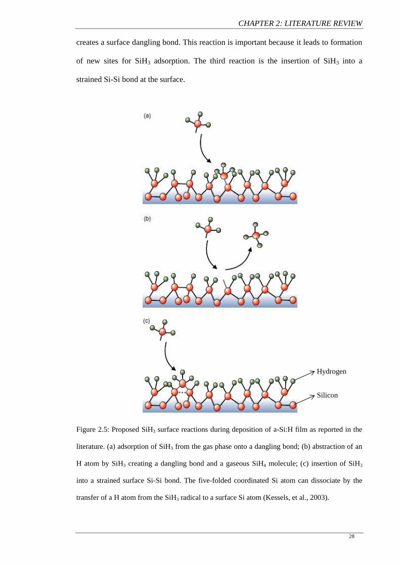
CHAPTER 2: LITERATURE REVIEW
28
creates a surface dangling bond. This reaction is important because it leads to formation
of new sites for SiH3 adsorption. The third reaction is the insertion of SiH3 into a
strained Si-Si bond at the surface.
Figure 2.5: Proposed SiH3 surface reactions during deposition of a-Si:H film as reported in the
literature. (a) adsorption of SiH3 from the gas phase onto a dangling bond; (b) abstraction of an
H atom by SiH3 creating a dangling bond and a gaseous SiH4 molecule; (c) insertion of SiH3
into a strained surface Si-Si bond. The five-folded coordinated Si atom can dissociate by the
transfer of a H atom from the SiH3 radical to a surface Si atom (Kessels, et al., 2003).
Hydrogen
Silicon
CHAPTER 2: LITERATURE REVIEW
29
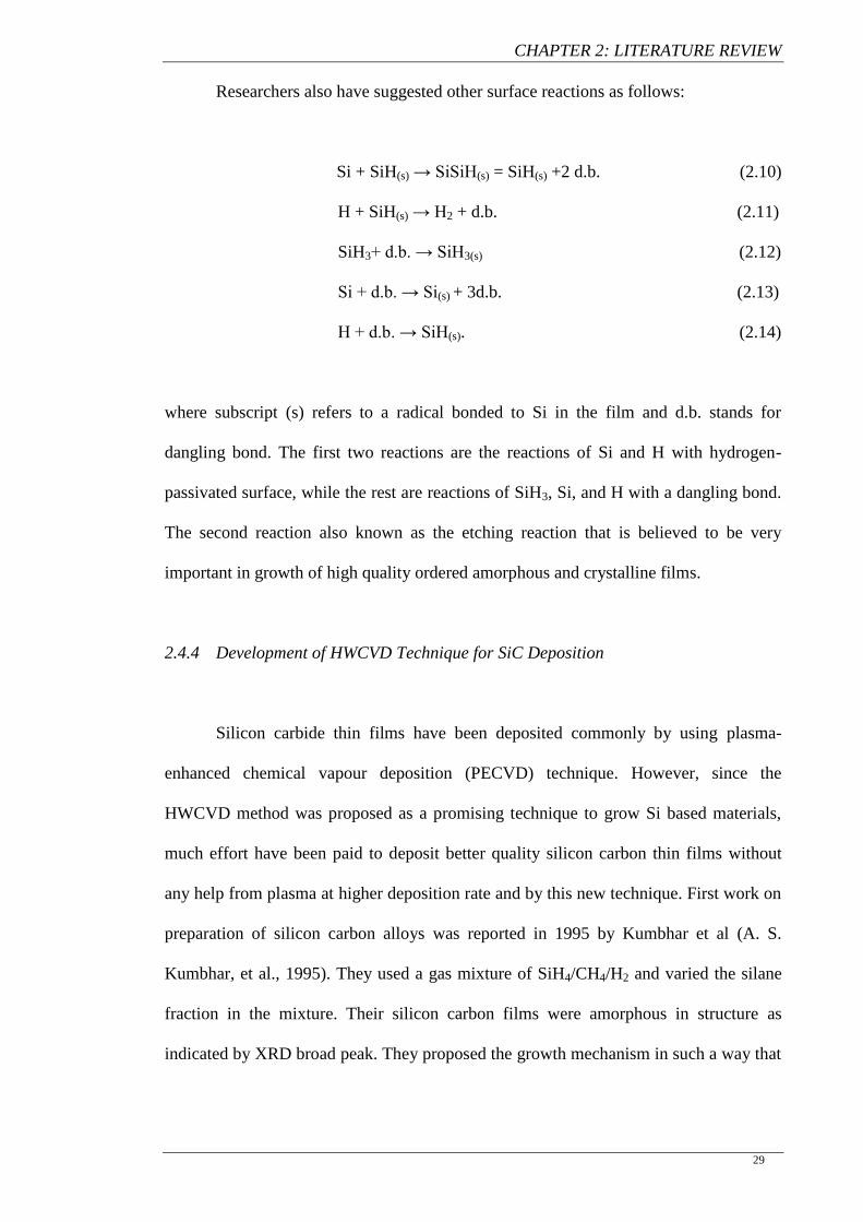
Researchers also have suggested other surface reactions as follows:
Si + SiH(s) → SiSiH(s) = SiH(s) +2 d.b. (2.10)
H + SiH(s) → H2 + d.b. (2.11)
SiH3+ d.b. → SiH3(s) (2.12)
Si + d.b. → Si(s) + 3d.b. (2.13)
H + d.b. → SiH(s). (2.14)
where subscript (s) refers to a radical bonded to Si in the film and d.b. stands for
dangling bond. The first two reactions are the reactions of Si and H with hydrogen-
passivated surface, while the rest are reactions of SiH3, Si, and H with a dangling bond.
The second reaction also known as the etching reaction that is believed to be very
important in growth of high quality ordered amorphous and crystalline films.
2.4.4 Development of HWCVD Technique for SiC Deposition
Silicon carbide thin films have been deposited commonly by using plasma-
enhanced chemical vapour deposition (PECVD) technique. However, since the
HWCVD method was proposed as a promising technique to grow Si based materials,
much effort have been paid to deposit better quality silicon carbon thin films without
any help from plasma at higher deposition rate and by this new technique. First work on
preparation of silicon carbon alloys was reported in 1995 by Kumbhar et al (A. S.
Kumbhar, et al., 1995). They used a gas mixture of SiH4/CH4/H2 and varied the silane
fraction in the mixture. Their silicon carbon films were amorphous in structure as
indicated by XRD broad peak. They proposed the growth mechanism in such a way that
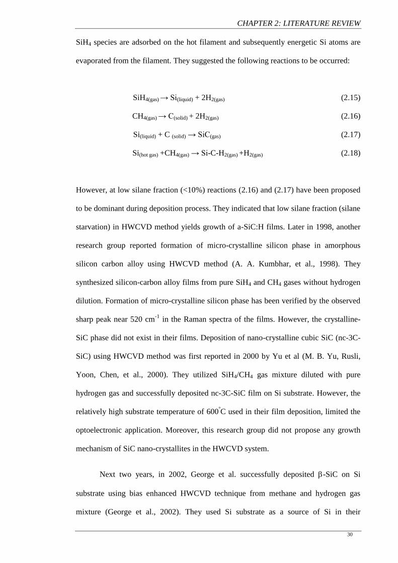
CHAPTER 2: LITERATURE REVIEW
30
SiH4 species are adsorbed on the hot filament and subsequently energetic Si atoms are
evaporated from the filament. They suggested the following reactions to be occurred:
SiH4(gas) → Si(liquid) + 2H2(gas) (2.15)
CH4(gas) → C(solid) + 2H2(gas) (2.16)
Si(liquid) + C (solid) → SiC(gas) (2.17)
Si(hot gas) +CH4(gas) → Si-C-H2(gas) +H2(gas) (2.18)
However, at low silane fraction (<10%) reactions (2.16) and (2.17) have been proposed
to be dominant during deposition process. They indicated that low silane fraction (silane
starvation) in HWCVD method yields growth of a-SiC:H films. Later in 1998, another
research group reported formation of micro-crystalline silicon phase in amorphous
silicon carbon alloy using HWCVD method (A. A. Kumbhar, et al., 1998). They
synthesized silicon-carbon alloy films from pure SiH4 and CH4 gases without hydrogen
dilution. Formation of micro-crystalline silicon phase has been verified by the observed
sharp peak near 520 cm-1
in the Raman spectra of the films. However, the crystalline-
SiC phase did not exist in their films. Deposition of nano-crystalline cubic SiC (nc-3C-
SiC) using HWCVD method was first reported in 2000 by Yu et al (M. B. Yu, Rusli,
Yoon, Chen, et al., 2000). They utilized SiH4/CH4 gas mixture diluted with pure
hydrogen gas and successfully deposited nc-3C-SiC film on Si substrate. However, the
relatively high substrate temperature of 600ºC used in their film deposition, limited the
optoelectronic application. Moreover, this research group did not propose any growth
mechanism of SiC nano-crystallites in the HWCVD system.
Next two years, in 2002, George et al. successfully deposited -SiC on Si
substrate using bias enhanced HWCVD technique from methane and hydrogen gas
mixture (George et al., 2002). They used Si substrate as a source of Si in their
CHAPTER 2: LITERATURE REVIEW
31
deposition. They found that the formation of highly oriented -SiC films was due to
applying of bias and use of low pressure during the deposition. The bias resulted in the
bombardment of the substrate and the growing film by high-energy positive ions. Low
pressure leads to the mean free path of the precursor species comparable to the distance
between filament and the substrate. However, this method has limitation of deposition
of SiC films at high temperatures (> 700°C) and only on Si substrate.
The interest in SiC deposition by HWCVD technique has been significantly
increased and many other researchers have attempted to prepare SiC films by this
technique in order to understand the properties of the resulting films as well as growth
mechanism of SiC films in HWCVD. However, different structures of SiC such as
amorphous, microcrystalline and nano-crystalline structures have been obtained from
different deposition conditions. For example, Tabata group have obtained amorphous
and nano-crystalline SiC films using SiH4/CH4/H2 gas mixture under different
conditions (A. Tabata, Hoshide, & Kondo, 2010; A. Tabata & Komura, 2007; A.
Tabata, Komura, Narita, & Kondo, 2009; A. Tabata, Kuroda, M., Mori, M., Mizutani,
T., Suzuoki, Y., 2004; A. Tabata & Mori, 2008). Chen et al. have deposited
microcrystalline SiC (c-SiC) films from decomposition of monomethylsilane (MMS)
diluted in H2 gas (Chen et al., 2012; Chen, Huang, Yang, Carius, & Finger, 2010; Chen,
Huang, Yang, Carius, & Finger, 2011; Chen, Yang, Carius, & Finger, 2010). It should
be noted that formation of this kind of SiC structure has only reported from HWCVD
using MMS as a source gas. It seems that the presence of Si-C bond in this molecule has
important role for growing stoichiometric and highly crystalline films. While deposition
of a-SiC embedded with nano- or micro-crystalline silicon by HWCVD has also been
reported by other groups (I. Ferreira, Fernandes, & Martins, 1999; Takashi Itoh, et al.,
2001; Mao, et al., 2012; Shen, et al., 2012). It has been shown that high hydrogen
dilution of the gas mixture enhances the formation of SiC crystallites into the films
CHAPTER 2: LITERATURE REVIEW
32
(Mao, et al., 2012; A. Tabata & Mori, 2008; Q. Zhao et al., 2004). In addition it has
been concluded that higher deposition pressures and filament temperature are suitable
condition for growth of nc-3C-SiC (Shen, et al., 2012; A. Tabata et al., 2006; A. Tabata,
et al., 2009; Wu, 2011; Q. Zhao, et al., 2004). Now, after about two decades from the
first SiC deposition by HWCVD technique, many aspects remained unknown. In
addition, because of lack of theoretical calculations and/or experimental measurement
of chemical reactions and radicals in the HWCVD of SiC, the growth mechanism of SiC
material from the SiH4 and CH4 gas mixture has not been explored clearly yet.
However, it is generally believed that presence of large flux of H radicals is required for
improvement of the crystallinity in SiC films. This is due to the effect of H radicals in
etching of the weak and strained bonds and nucleation for crystalline growth.
Beside studies on growth of SiC films by HWCVD, some attempts have been
taken toward doping of amorphous and crystalline SiC to improve the electrical
properties for potential applications in optoelectronic devices such as solar cells. T. Itoh
et al. have shown for the first time the possibility of doping of a-SiC films including c-
Si grains by HWCVD technique using B2H6 and PH3 gases for n-type and p-type
doping, respectively (T. Itoh, Fukunaga, Katoh, Fujiwara, & Nonomura, 2002; Takashi
Itoh, et al., 2001). They demonstrated that the dark and photoconductivity of the B- and
P-doped films was larger than undoped samples. A year later, Miyajima’s group
successfully fabricated a-Si solar cells with p-layer (B-doped a-SiC films containing c-
Si grains) and obtained a conversion efficiency of 10.2% (Shinsuke Miyajima, Yamada,
& Konagai, 2003). They also deposited n- and p-type nano-crystalline cubic SiC films
by HWCVD. It has been shown that p-type doping significantly affected absorption
coefficients above the band gap of nc-3C-SiC:H compared with n-type doping
(Shinsuke Miyajima, Yamada, & Konagai, 2007). Recently, several works have been
reported the development in application of microcrystalline SiC films deposited by

CHAPTER 2: LITERATURE REVIEW
33
HWCVD as transparent window layer in silicon solar cells (Chen, et al., 2012; Chen,
Huang, et al., 2010; Chen, et al., 2011; Mao, et al., 2012).
It is concluded that the HWCVD method is a promising deposition technique for
preparing device quality SiC films. Therefore, more information about the details of SiC
growth mechanism and influence of various deposition parameters on the properties of
SiC films deposited using this technique would be useful for further development in this
field.
CHAPTER 3: EXPERIMENTAL METHODS
34
CHAPTER 3
Experimental
and
Analytical Procedure
CHAPTER 3: EXPERIMENTAL METHODS
35
3.1 Introduction
The SiC thin films were deposited using a home-built hot-wire chemical vapour
deposition, HWCVD system and characterized by using a series of characterization
methods. This chapter contains two main parts, the experimental and analytical methods
involved in this work. The first part of this chapter describes the HWCVD deposition
system, pre-deposition, and film deposition procedures, while the second part of this
chapter presents the instruments, characterization procedure and calculation methods
utilized in characterizing the films and analysis of results. These characterization
methods include mechanical profilometry, Fourier transform infrared spectroscopy
(FTIR), Micro-Raman scattering spectroscopy, X-ray diffraction (XRD), Auger electron
spectroscope (AES), field emission scanning electron microscope (FESEM), UV-Vis-
NIR spectroscopy, and photoluminescence (PL) spectroscopy.
3.2 Hot-Wire Chemical Vapour Deposition (HWCVD) System
In this work, a home-built HWCVD system in the low dimensional material
research centre (LDMRC), University of Malaya, was utilized for deposition of SiC thin
films. This system comprises a reaction chamber, a vacuum pumping system, the gases
supply and distribution system, the electrical power supply system, and detoxification
system. A schematic diagram of the HWCVD system used in this study is shown in
Figure 3.1.
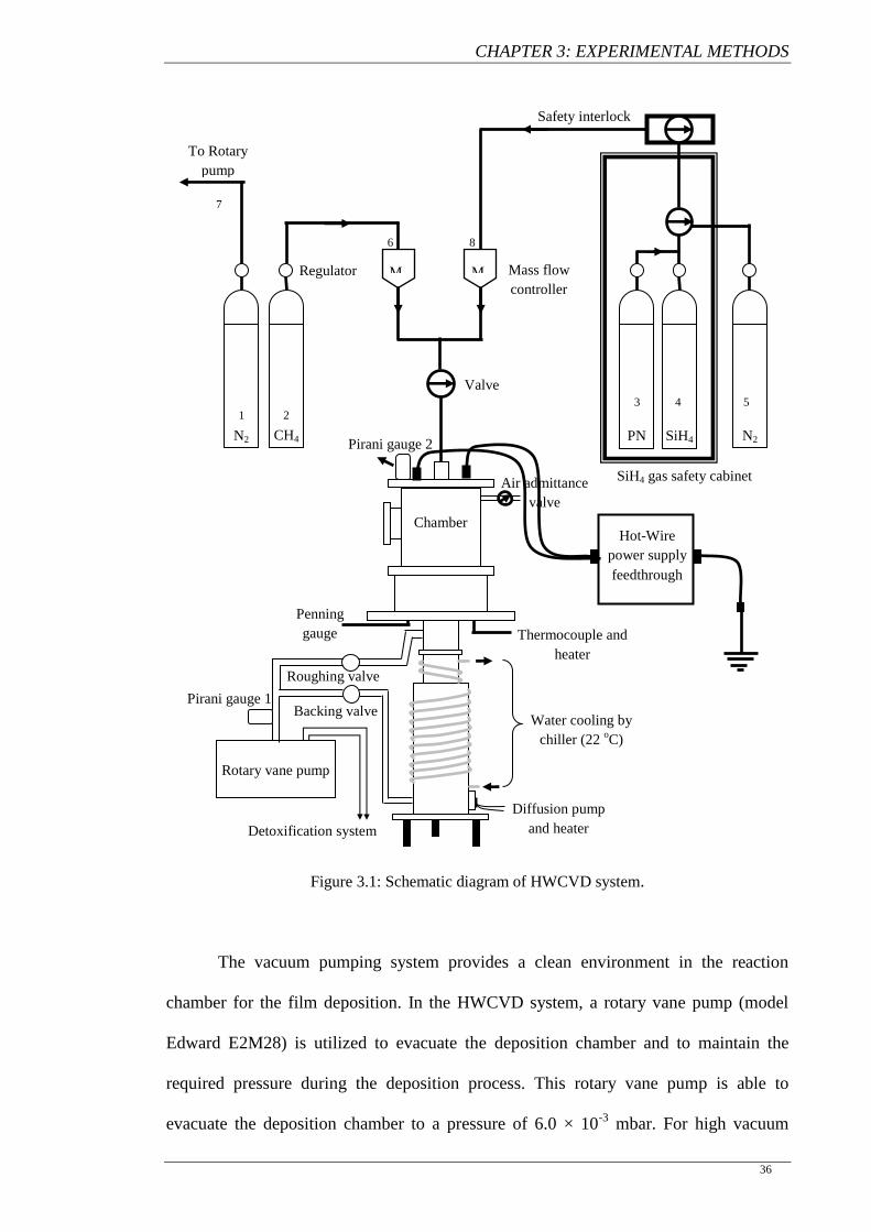
CHAPTER 3: EXPERIMENTAL METHODS
36
Figure 3.1: Schematic diagram of HWCVD system.
The vacuum pumping system provides a clean environment in the reaction
chamber for the film deposition. In the HWCVD system, a rotary vane pump (model
Edward E2M28) is utilized to evacuate the deposition chamber and to maintain the
required pressure during the deposition process. This rotary vane pump is able to
evacuate the deposition chamber to a pressure of 6.0 × 10⁻³
mbar. For high vacuum
SiH4 gas safety cabinet
N2 SiH4 PN CH4 N2
M M
Hot-Wire
power supply
feedthrough
Thermocouple and
heater
Roughing valve
Rotary vane pump
Diffusion pump
and heater
Mass flow
controller
Safety interlock
Chamber
Water cooling by
chiller (22 oC)
Valve
Air admittance
valve
Regulator
1 2 3 4 5
6
7
8
Pirani gauge 1 Backing valve
Penning
gauge
Pirani gauge 2
Detoxification system
To Rotary
pump
CHAPTER 3: EXPERIMENTAL METHODS
37
condition, the chamber is pumped down until base pressure is as low as 2.0 × 10 -5
mbar
for 1 hour pumping by diffusion pump (model Edward F603 with heating power of
1300 W). The cooling system for the diffusion pump is circulated by chiller to enhance
pumping efficiency of the diffusion pump. The cooling temperature of the chiller is
fixed at 22°C. The pressure in the chamber for low and high level vacuum is measured
using pirani (Leybold vacuum gauge with model TTR91) and penning (Leybold
vacuum gauge with model PTR 225) gauge respectively.
The rotary vane pump is connected to a 10 kVA Uninterruptible Power Supply
(UPS) in order to make sure that there is no abrupt interruption in the power supply
during the deposition. This UPS can sustain the power supply for about 2 hours when
there is any break in power supply. This is to confirm that silane gas is always in
pumping and vacuum condition.
The nitrogen gas is used to purge the gas line and reaction chamber before and
after deposition to remove any contaminants in the gas lines and deposition system. In
addition, the nitrogen gas is directed into the rotary vane pump to prevent the silane gas
from condensing in the pump during deposition and to dilute the gas before leaving
through the exhaust lines. The excess silane gas exits via the exhaust line into the
detoxification system, which is located outside the laboratory.
A cross-sectional overview of HWCVD reaction chamber is shown in Figure
3.2. The chamber is made of stainless steel, which is a passive material in the presence
of the reactant gases. The dimensions of the reaction chamber are 200 mm in height,
180 mm in diameter and 6 mm in wall thickness. The mixed source gases enter the
chamber from the top plate through a shower head and exit from the bottom of the
chamber to the rotary pump. Two stainless steel rods are the filament holders, which are
connected to the top plate of the chamber. These holders are connected to the DC power
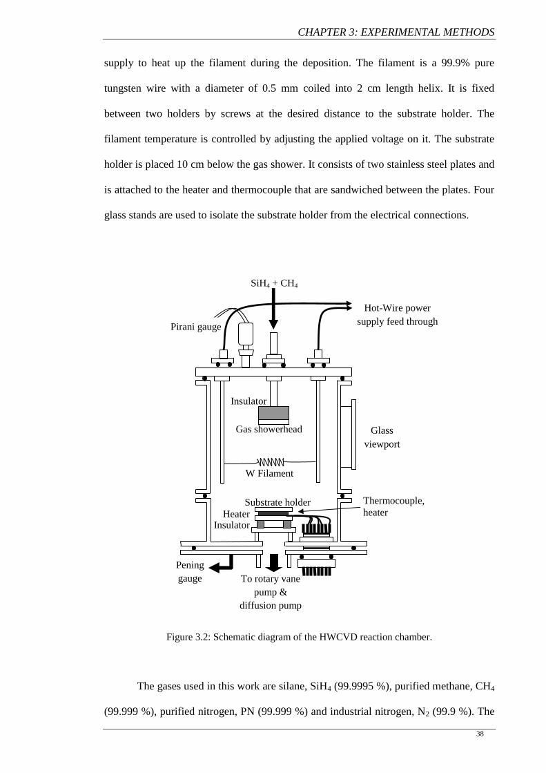
CHAPTER 3: EXPERIMENTAL METHODS
38
supply to heat up the filament during the deposition. The filament is a 99.9% pure
tungsten wire with a diameter of 0.5 mm coiled into 2 cm length helix. It is fixed
between two holders by screws at the desired distance to the substrate holder. The
filament temperature is controlled by adjusting the applied voltage on it. The substrate
holder is placed 10 cm below the gas shower. It consists of two stainless steel plates and
is attached to the heater and thermocouple that are sandwiched between the plates. Four
glass stands are used to isolate the substrate holder from the electrical connections.
Figure 3.2: Schematic diagram of the HWCVD reaction chamber.
The gases used in this work are silane, SiH4 (99.9995 %), purified methane, CH4
(99.999 %), purified nitrogen, PN (99.999 %) and industrial nitrogen, N2 (99.9 %). The
Pening
gauge
SiH4 + CH4
Hot-Wire power
supply feed through
Glass
viewport
Gas showerhead
Substrate holder
Heater
To rotary vane
pump &
diffusion pump
Thermocouple,
heater
Insulator
Insulator
W Filament
Pirani gauge
CHAPTER 3: EXPERIMENTAL METHODS
39
SiH4 and CH4 are used as the source gas for Si and C in SiC thin films deposition, while
PN and N2 are used for purging the HWCVD system, which includes the gas line,
reaction chamber and roughing after every deposition. All these gases are distributed
from the gas cylinders inside the gas room to the reaction chamber. The gases are
carried through ¼” stainless steel tubing using Swagelock connectors and valves to a
gas distribution panel.
The SiH4 is a highly inflammable gas and thus, its cylinder is kept in the safety
cabinet attached to an exhaust system which is able to remove any SiH4 gas in case of
leakage. A photograph of this safety cabinet is shown in Figure 3.3. The SiH4 gas
cylinder has a special gas regulator, model AP1510S, which is connected to a special
purging system. This purging system is connected to an N2 gas cylinder. This special
gas regulator has a pneumatic valve, which allows gas through it only when the pressure
of N2 is about 50 psi. This N2 gas is connected to the regulator through a safety system.
This safety system, which is particularly used for SiH4 gas can stop the SiH4 gas from
flowing into the chamber instantly in the case of emergency.
From the gas distribution panel, the gases separately pass through metering
valves (Swagelock, SS-4MG) and then the mass flow controller (MFC) with model
(Aalborg, GFC17), to display the gas flow-rate. Metering valves control the gas
pressure to avoid high pressure gases entering the MFC. On exiting the MFC, the gases
pass through check valves (Swagelock, SS-CHS4-1/3) which are used to prevent back
flow of the gases. The gases are mixed before inflowing to the reaction chamber.
For the SiH4 gas, the bypass line is provided for safety purposes, which allow
the SiH4 gas to be pumped out via the rotary pump directly if any blockage occurs at the
entrance of the MFC. Also, it is used to remove excess SiH4 and other gases at a faster
purging rate after the deposition process.
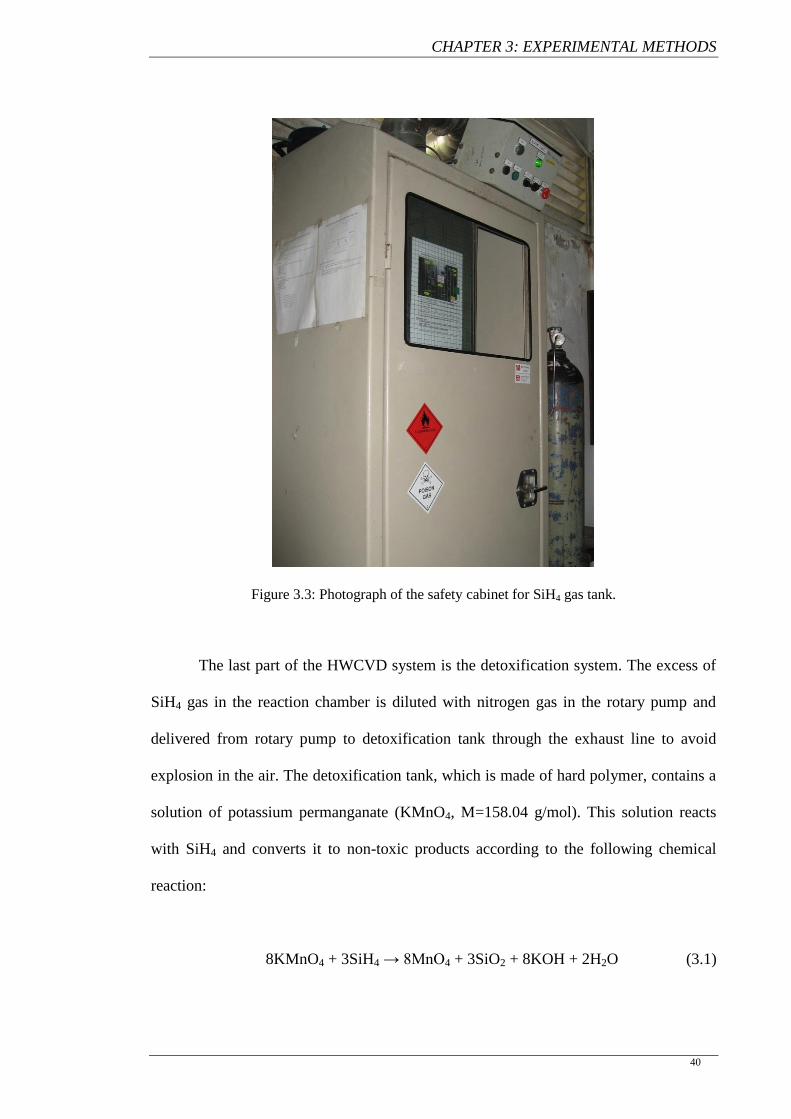
CHAPTER 3: EXPERIMENTAL METHODS
40
Figure 3.3: Photograph of the safety cabinet for SiH4 gas tank.
The last part of the HWCVD system is the detoxification system. The excess of
SiH4 gas in the reaction chamber is diluted with nitrogen gas in the rotary pump and
delivered from rotary pump to detoxification tank through the exhaust line to avoid
explosion in the air. The detoxification tank, which is made of hard polymer, contains a
solution of potassium permanganate (KMnO4, M=158.04 g/mol). This solution reacts
with SiH4 and converts it to non-toxic products according to the following chemical
reaction:
8KMnO4 + 3SiH4 → 8MnO4 + 3SiO2 + 8KOH + 2H2O (3.1)
CHAPTER 3: EXPERIMENTAL METHODS
41
This process starts from the opening of the SiH4 gas line until a few hours after
deposition.
The electrical power supply system includes two parts, the DC power supply for
the filament heating, and the power supply for the substrate heating. An automatic
voltage regulator (VMARK AVR-1000VA) is connected to the substrate heater to
stabilize the voltage. The applied voltage to the filament and the substrate is adjusted by
the voltage regulator (IBC Regavolt, 0-240 V A.C., 1 KVA). A temperature controller
(Taishio TS501) is used to monitor the substrate temperature during the deposition
process. The substrate temperature is measured by a chromel-alumel k-type
thermocouple, which operates from room temperature up to 500ºC.
3.3 Sample Preparation
3.3.1 Pre-deposition Procedure
Before film deposition, it is essential to clean the substrates and filament
according to the standard procedures in order to avoid absorption of dusts and
contaminations in the film during the deposition.
3.3.1.1 Substrate Cleaning
In this work, SiC films are deposited on glass and p-type c-Si (111)
simultaneously. They are first cut into 2 cm × 2 cm squares. Before deposition, it is
essential to clean the substrates properly to remove any types of contamination from the
substrate surface in order to deposit films having better properties. The method of
substrate cleaning varies for different substrates.
CHAPTER 3: EXPERIMENTAL METHODS
42
For cleaning the glass substrates, they are placed in a clean beaker and rinsed
with deionized water several times. Then they are immersed in a beaker containing soap
solution (Decon 90 diluted with distilled water). Next, this beaker is placed in the
ultrasonic bath for 15 minutes followed by rinsing with deionized water. Finally, they
are immersed in acetone and ethanol, and dried thoroughly by industrial nitrogen gas.
The cleaning process for the c-Si substrates starts with rinsing the substrates
with deionized water similar to glass substrates. Then, they are immersed in a beaker
containing H2O:HCL:H2O2 = 86:11:3 solution for 6 minutes to remove inorganic
contaminations from the Si-substrate surface. Then, the substrates are rinsed again with
deionized water. The Si substrates are then put in a beaker containing a solution of
H2O:H2O2:NH4OH = 4:1:1 for 6 minutes followed by rinsing with deionized water to
remove any organic contaminations. Finally, the Si-substrates are immersed in a
solution of H2O: HF = 10:1 for 6 minutes and then rinsed with deionized water to
remove native oxides from the Si surface. The last step is to dry the substrates using
nitrogen gas.
After the cleaning process, the cleaned substrates are immediately put into the
reaction chamber, which is directly pumped down.
3.3.1.2 Filament Pre-heating
The W filament was pre-heated before every deposition to remove existing
oxides from the filament surface. For this purpose, the W-filament was heated at 1900ºC
under flow of hydrogen gas (40 sccm) for 10 minutes. The procedure of filament pre-
heating is carried out after evacuation of the system by rotary pump to the pressure of
8×10⁻³
mbar.
CHAPTER 3: EXPERIMENTAL METHODS
43
3.3.2 Film Deposition Procedure
In order to deposit SiC thin films, it is important to ensure that all the
components of the reaction chamber are clean. The cleaning of the chamber’s wall and
components is performed first by rubbing with sand paper and then cleaning thoroughly
with acetone.
After cleaning the chamber and the substrates, the latter are fixed on the
substrate holder by using a stainless steel mask. It is of importance to double check all
the electrical connections of the substrate heater, thermocouple, and the filament before
closing the chamber. Next, the chamber is completely sealed to prevent any leakage,
and evacuated by using rotary and diffusion pump. Before turning on the rotary pump, it
is required to check and ensure that all the valves in the system are closed. After starting
the rotary pump and the pressure display, the roughing valve should be slowly opened
until fully opened to prevent damaging the pump. The rotary pump is able to evacuate
the system to 6 × 10⁻³
mbar in 1-2 hours. During this stage, it is important to empty all
the gas lines from the gas tank to the chamber. For this purpose, all the valves of SiH4
and CH4 lines including metering valves, MFCs, and valves in the distribution panel are
opened respectively from the chamber to the tank. After the pressure 6 × 10⁻³
mbar is
obtained, the metering valves are closed and the MFCs are switched off. The diffusion
pump would help to reach the base pressure of 2 × 10⁻⁵
mbar after around 1 hour. To
start pumping with diffusion pump it is essential to turn on the water chiller 30 minutes
before heating the diffusion pump. This, makes the body of diffusion pump cold (22ºC)
and enhances the pumping efficiency. The last step before switching on the diffusion
pump is opening the backing valve and waiting until the pressure becomes stable. The
diffusion pump is then switched on and left to warm up for about 30 to 40 minutes
before opening the high vacuum valve. A fan is usually used to prevent excess heating
CHAPTER 3: EXPERIMENTAL METHODS
44
at the bottom part of the diffusion pump. Before opening main vacuum valve, the
roughing valve must be completely closed. Afterwards, the high vacuum valve is
gradually opened. Now, the pressure is decreasing with higher rate and to lower values.
After the pressure of 2 × 10⁻⁵
mbar is obtained, the high vacuum valve is slowly closed
and the roughing valve is opened again. The diffusion pump is then switched off while
the cooling system is kept operating to cool the body of the diffusion pump. Then, the
backing valve is closed tightly. The next step before starting the film deposition is
heating the substrates to reach the desired temperature. In this work, the substrate
temperature is always kept constant at 300ºC and set to this value by the temperature
controller. Subsequently, the heating is started by applying the AC voltage of 80 V by
Regavolt. Once the temperature of substrates reaches 300ºC and the pressure is stable,
the gases are flowing into the chamber. Before SiH4 is allowed to flow into the
deposition chamber, the N2 gas cylinder (see Figure 3.2, labelled as 5) is opened. This
will automatically turn on the pneumatic valve and allow the SiH4 gas to flow through
it. The excess flow switch (EFS) in the gas line will be activated if the SiH4 pressure in
the line is abruptly increased above 70 psi and the alarm in the safety cabinet will ring.
Concurrently, nitrogen gas labelled as 1 in Figure 3.2, is allowed to flow into the rotary
pump in order to dilute the excess SiH4 gas during deposition for safety purposes. To
flow the SiH4 into the reaction chamber, first the SiH4 gas tank is opened slightly until
the gas pressure reaches 100 psi and then the valve is closed. Then the MFC of SiH4 is
switched on and the metering valve slowly opened. The CH4 gas flows into the reaction
chamber simply by opening the gas tank followed by switching on the CH4 MFC and
opening the corresponding metering valve. The flow rates of SiH4 and CH4 are
monitored by their individual MFCs as fixed at the desired values for every film
deposition. The deposition pressure is controlled by adjusting the roughing valve
connected to the reaction chamber.
CHAPTER 3: EXPERIMENTAL METHODS
45
The deposition process begins when the filament is heated up until 1900ºC by
applying AC voltage to it. The voltage must be gradually increased from zero until the
filament temperature reaches 1900ºC. First stages of increasing the applied voltage
should be done very carefully and slowly to prevent sudden expansion of filament and
likely deformation or disconnection of the filament. The temperature of the filament is
monitored by an optical pyrometer (model Raytek), which operates at spectral range of
1.0 μm. The emissivity value is set at 0.35 as mentioned in the pyrometer’s manual. The
deposition time is started once the filament temperature reaches 1900ºC, and is ended
when the applied voltage is decreased to zero. The deposition time is fixed at 30
minutes for every deposition. During the deposition, all the deposition parameters
including substrate temperature, deposition pressure, filament temperature, and gases
flow rates are monitored and maintained. However, the radiations from the hot filament
sometimes influence the substrate temperatures. This depends mostly on the distance
between filament and substrates. The variation of substrate temperature because of
filament radiation during the deposition process for two sets of samples prepared at
different deposition pressure and filament-to-substrate distance is shown in Figure 3.4.
From this figure, it is seen that the substrate temperature is almost independent of
deposition pressure. Similar results were observed for the films deposited at various gas
flow rates and gas pressures. Nevertheless, it was found that the decrease in the distance
between substrate and filament significantly increased the substrate temperature.
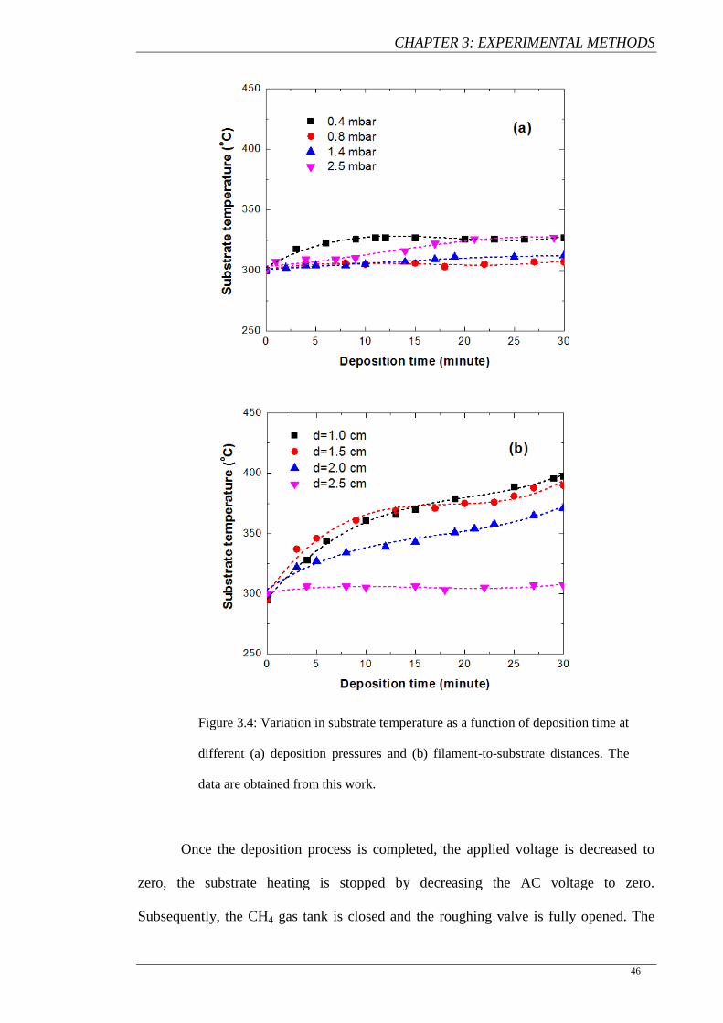
CHAPTER 3: EXPERIMENTAL METHODS
46
Figure 3.4: Variation in substrate temperature as a function of deposition time at
different (a) deposition pressures and (b) filament-to-substrate distances. The
data are obtained from this work.
Once the deposition process is completed, the applied voltage is decreased to
zero, the substrate heating is stopped by decreasing the AC voltage to zero.
Subsequently, the CH4 gas tank is closed and the roughing valve is fully opened. The
CHAPTER 3: EXPERIMENTAL METHODS
47
gas lines are pumped until the pressure reaches the pre-deposition pressure. This means
that all gases are finished, which is also indicated by the MFCs that show zero flow rate
for both SiH4 and CH4 gases. This verifies that no excess gas remains in the gas lines.
Subsequently, the SiH4 line must be purged by purified nitrogen gas several times to
flush out any excess silane in the gas line. For this purpose, firstly, the valve in the SiH4
line to the system is closed. Then, the PN gas tank (labelled as 3 in Figure 3.1) is
opened to fill the SiH4 line with the nitrogen gas and then it is closed. Subsequently, the
valve on the SiH4 line is opened to allow nitrogen to flow in the line with high pressure
through the metering valve and MFC toward the chamber. The pumping is continued
until the nitrogen gas pressure reaches zero. This action is repeated several times to
ensure that all the excess SiH4 gases are purged from the line.
When all gases in the lines are pumped out and the system evacuated until the
pressure of 6 × 10⁻³
mbar, we just have to wait until the samples are cooled down to
near room temperature. The system can be switched off by closing all the gas valves and
roughing valve and switching off the rotary pump. Now, the chamber can be opened in
order to take out the deposited films for characterization. The films are transferred into a
clean sample container and kept in the dry cabinet for future characterizations.
In this work, the filament and substrate temperatures were fixed at 1900ºC and
300ºC; respectively for deposition of total six sets of silicon carbide thin films. Two sets
of samples were deposited by varying the CH4 gas flow rate from 10 to 100 sccm while
SiH4 flow rate was fixed at 0.5 and 1 sccm. To investigate the effect of gas pressure,
two sets of films were prepared at fixed SiH4 to CH4 flow rate ratio of 0.05 while the
total gas partial pressure was varied from 12 to 33 Pa. For one set, the deposition
pressure was kept constant at 80 Pa by adjusting the roughing valve, and in another set,
the deposition pressure was equal to the total gas partial pressure by leaving the
CHAPTER 3: EXPERIMENTAL METHODS
48
roughing valve fully opened. Lastly, the effect of deposition pressure and the filament-
to-substrate distance (d) on the properties of SiC films were studied by preparing films
at SiH4 and CH4 flow rates of 1 and 20 sccm, respectively, and changing the deposition
pressure and d.
3.4 Characterization and Analytical Procedures
This section describes the characterization and analytical procedures performed
to characterize the SiC films and analyse the data obtained. These characterization
techniques include surface profilometery to determine the film thickness and deposition
rate, Fourier transform infrared (FTIR) spectroscopy and Raman scattering spectroscopy
to investigate the bonding configurations, Auger electron spectroscopy (AES) for
elemental composition, field emission scanning electron microscope (FESEM) to study
the morphology, and UV-Vis-NIR spectroscopy for optical characterization of the films.
3.4.1 Thickness Measurement by Surface Profilometry
The thickness of SiC films deposited on glass and c-Si was determined using a
KLA-Tencor P-6 surface profiler system, shown in Figure 3.5, which works in contact
mode.
Before SiC film deposition, a mask was placed on the substrates in order to
create a well-defined edge between substrate and SiC film. The profiler measures the
step height between the edge of the film and the substrate. A horizontal scan across the
step from the substrate to the middle of the film provides the thickness of the film
deposited on the substrate. The average of four measurements from different edges was
taken as the average film thickness.
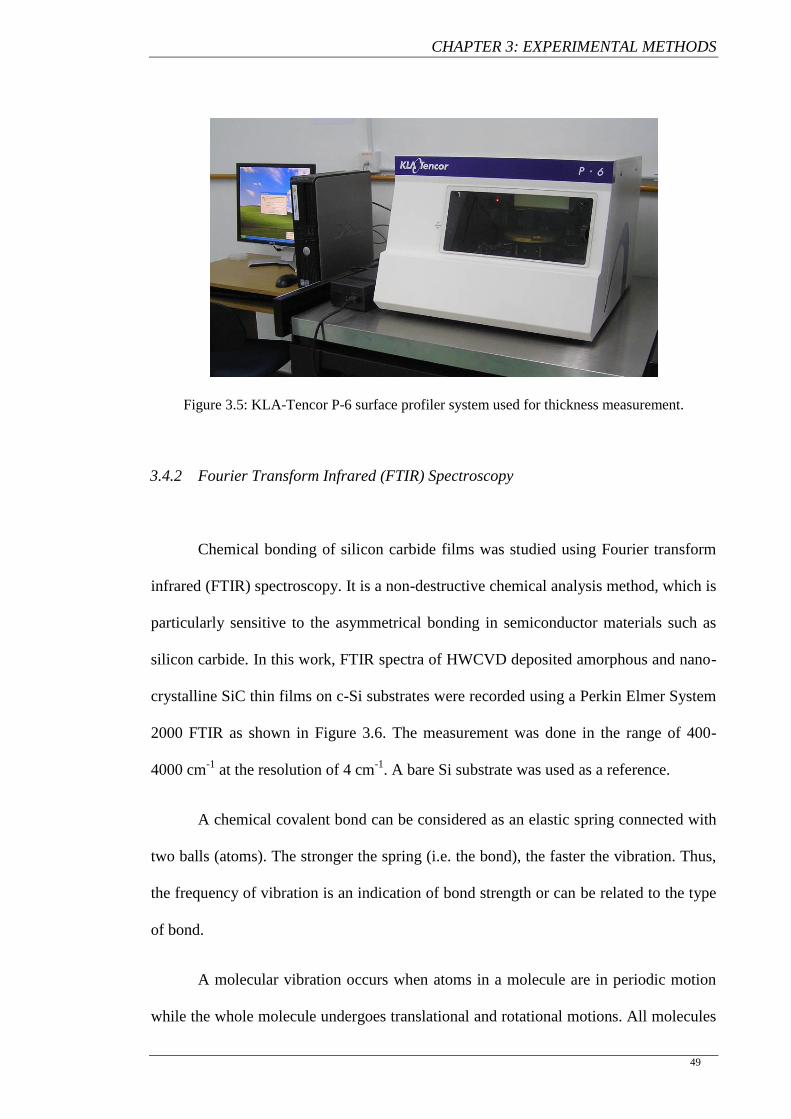
CHAPTER 3: EXPERIMENTAL METHODS
49
Figure 3.5: KLA-Tencor P-6 surface profiler system used for thickness measurement.
3.4.2 Fourier Transform Infrared (FTIR) Spectroscopy
Chemical bonding of silicon carbide films was studied using Fourier transform
infrared (FTIR) spectroscopy. It is a non-destructive chemical analysis method, which is
particularly sensitive to the asymmetrical bonding in semiconductor materials such as
silicon carbide. In this work, FTIR spectra of HWCVD deposited amorphous and nano-
crystalline SiC thin films on c-Si substrates were recorded using a Perkin Elmer System
2000 FTIR as shown in Figure 3.6. The measurement was done in the range of 400-
4000 cm-1
at the resolution of 4 cm-1
. A bare Si substrate was used as a reference.
A chemical covalent bond can be considered as an elastic spring connected with
two balls (atoms). The stronger the spring (i.e. the bond), the faster the vibration. Thus,
the frequency of vibration is an indication of bond strength or can be related to the type
of bond.
A molecular vibration occurs when atoms in a molecule are in periodic motion
while the whole molecule undergoes translational and rotational motions. All molecules
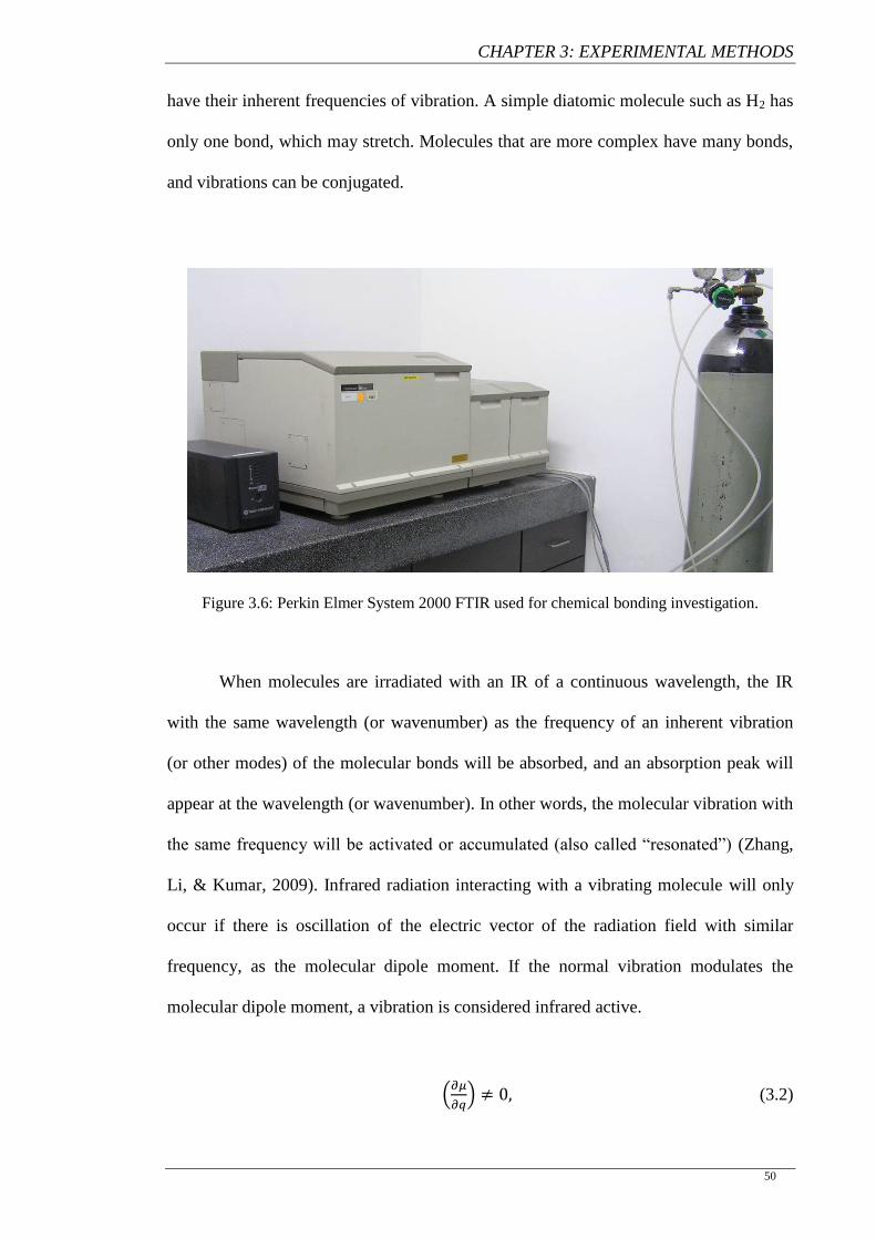
CHAPTER 3: EXPERIMENTAL METHODS
50
have their inherent frequencies of vibration. A simple diatomic molecule such as H2 has
only one bond, which may stretch. Molecules that are more complex have many bonds,
and vibrations can be conjugated.
Figure 3.6: Perkin Elmer System 2000 FTIR used for chemical bonding investigation.
When molecules are irradiated with an IR of a continuous wavelength, the IR
with the same wavelength (or wavenumber) as the frequency of an inherent vibration
(or other modes) of the molecular bonds will be absorbed, and an absorption peak will
appear at the wavelength (or wavenumber). In other words, the molecular vibration with
the same frequency will be activated or accumulated (also called “resonated”) (Zhang,
Li, & Kumar, 2009). Infrared radiation interacting with a vibrating molecule will only
occur if there is oscillation of the electric vector of the radiation field with similar
frequency, as the molecular dipole moment. If the normal vibration modulates the
molecular dipole moment, a vibration is considered infrared active.
(
) (3.2)
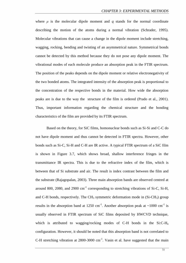
CHAPTER 3: EXPERIMENTAL METHODS
51
where μ is the molecular dipole moment and q stands for the normal coordinate
describing the motion of the atoms during a normal vibration (Schrader, 1995).
Molecular vibrations that can cause a change in the dipole moment include stretching,
wagging, rocking, bending and twisting of an asymmetrical nature. Symmetrical bonds
cannot be detected by this method because they do not pose any dipole moment. The
vibrational modes of each molecule produce an absorption peak in the FTIR spectrum.
The position of the peaks depends on the dipole moment or relative electronegativity of
the two bonded atoms. The integrated intensity of the absorption peak is proportional to
the concentration of the respective bonds in the material. How wide the absorption
peaks are is due to the way the structure of the film is ordered (Prado et al., 2001).
Thus, important information regarding the chemical structure and the bonding
characteristics of the film are provided by its FTIR spectrum.
Based on the theory, for SiC films, homonuclear bonds such as Si-Si and C-C do
not have dipole moment and thus cannot be detected in FTIR spectra. However, other
bonds such as Si-C, Si-H and C-H are IR active. A typical FTIR spectrum of a SiC film
is shown in Figure 3.7, which shows broad, shallow interference fringes in the
transmittance IR spectra. This is due to the refractive index of the film, which is
between that of Si substrate and air. The result is index contrast between the film and
the substrate (Rajagopalan, 2003). Three main absorption bands are observed centred at
around 800, 2080, and 2900 cm-1
corresponding to stretching vibrations of Si-C, Si-H,
and C-H bonds, respectively. The CH3 symmetric deformation mode in (Si-CH3) group
results in the absorption band at 1250 cm-1
. Another absorption peak at ~1000 cm-1
is
usually observed in FTIR spectrum of SiC films deposited by HWCVD technique,
which is attributed to wagging/rocking modes of C-H bonds in the Si:C-Hn
configuration. However, it should be noted that this absorption band is not correlated to
C-H stretching vibration at 2800-3000 cm-1
. Vasin et al. have suggested that the main
CHAPTER 3: EXPERIMENTAL METHODS
52
contribution of the absorption band at 2800-3000 cm-1
comes from hydrogenated carbon
clusters, i.e. from vibration of carbon-hydrogen bonds in the C:C-H configuration, while
the contribution of Si:C-Hn bonds is minor (Vasin, 2008).
In order to analyse FTIR results quantitatively, it is important that the absorption
coefficient (α(ω)) for the films should be measured, which can be done employing
Lambert-Beer’s law:
( )
[ ( ) ( )] (3.3)
where d is the film thickness and T0(ω) is the fitted baseline corresponding to zero
absorption as indicated by a dashed line in Figure 3.7.
Figure 3.7: A typical FTIR spectrum for silicon carbide films. The dashed line is the baseline
used to subtract the interference fringes in the spectrum.
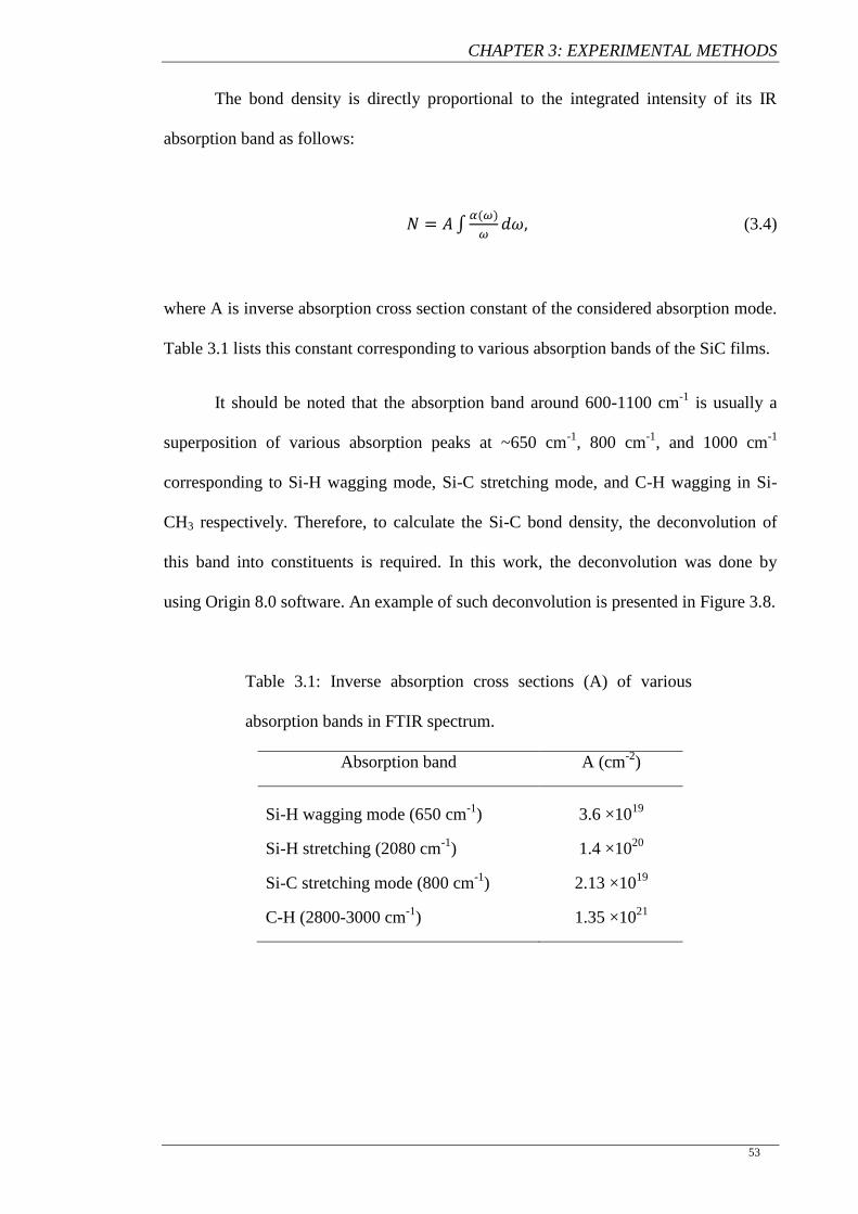
CHAPTER 3: EXPERIMENTAL METHODS
53
The bond density is directly proportional to the integrated intensity of its IR
absorption band as follows:
∫ ( )
(3.4)
where A is inverse absorption cross section constant of the considered absorption mode.
Table 3.1 lists this constant corresponding to various absorption bands of the SiC films.
It should be noted that the absorption band around 600-1100 cm-1
is usually a
superposition of various absorption peaks at ~650 cm-1
, 800 cm-1
, and 1000 cm-1
corresponding to Si-H wagging mode, Si-C stretching mode, and C-H wagging in Si-
CH3 respectively. Therefore, to calculate the Si-C bond density, the deconvolution of
this band into constituents is required. In this work, the deconvolution was done by
using Origin 8.0 software. An example of such deconvolution is presented in Figure 3.8.
Table 3.1: Inverse absorption cross sections (A) of various
absorption bands in FTIR spectrum.
Absorption band A (cm-2
)
Si-H wagging mode (650 cm-1
)
Si-H stretching (2080 cm-1
)
3.6 ×10¹⁹
1.4 ×10²⁰
Si-C stretching mode (800 cm-1
) 2.13 ×10¹⁹
C-H (2800-3000 cm-1
) 1.35 ×10²¹
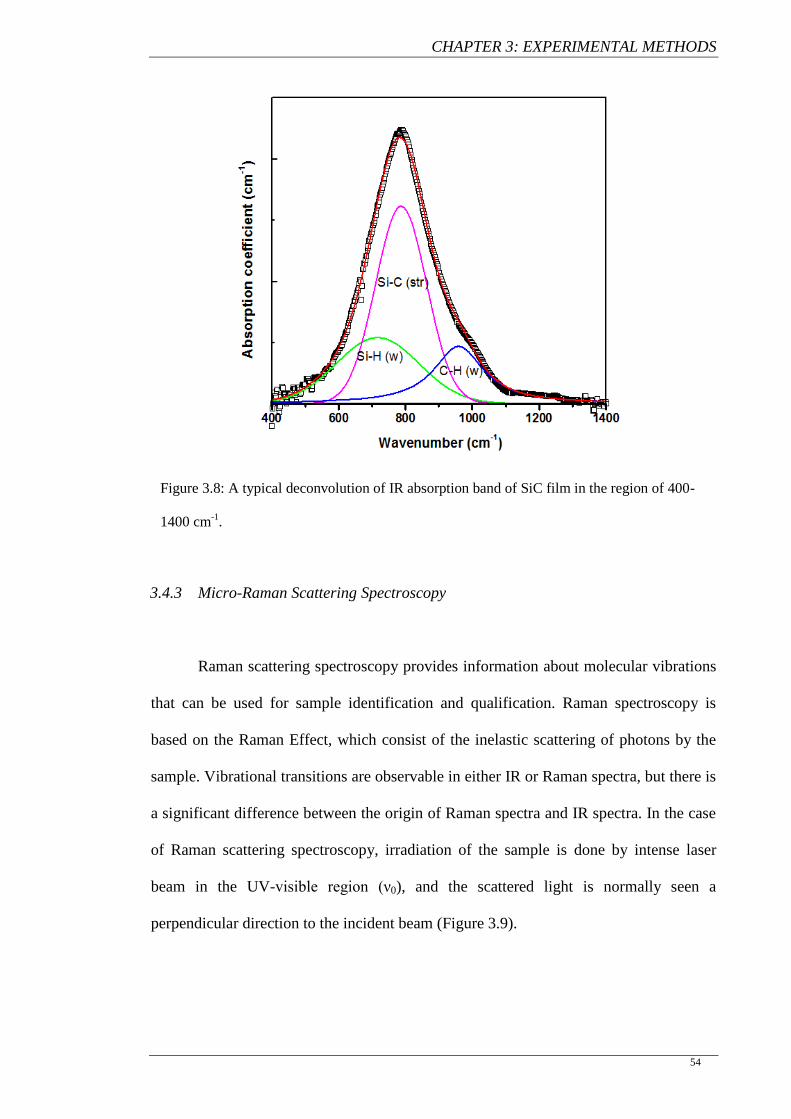
CHAPTER 3: EXPERIMENTAL METHODS
54
Figure 3.8: A typical deconvolution of IR absorption band of SiC film in the region of 400-
1400 cm-1
.
3.4.3 Micro-Raman Scattering Spectroscopy
Raman scattering spectroscopy provides information about molecular vibrations
that can be used for sample identification and qualification. Raman spectroscopy is
based on the Raman Effect, which consist of the inelastic scattering of photons by the
sample. Vibrational transitions are observable in either IR or Raman spectra, but there is
a significant difference between the origin of Raman spectra and IR spectra. In the case
of Raman scattering spectroscopy, irradiation of the sample is done by intense laser
beam in the UV-visible region (ν0), and the scattered light is normally seen a
perpendicular direction to the incident beam (Figure 3.9).
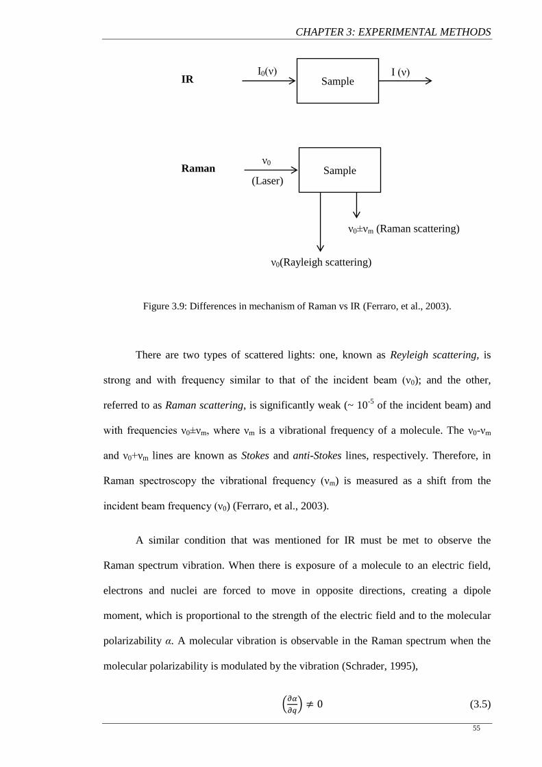
CHAPTER 3: EXPERIMENTAL METHODS
55
Figure 3.9: Differences in mechanism of Raman vs IR (Ferraro, et al., 2003).
There are two types of scattered lights: one, known as Reyleigh scattering, is
strong and with frequency similar to that of the incident beam (ν0); and the other,
referred to as Raman scattering, is significantly weak (~ 10-5
of the incident beam) and
with frequencies ν0±νm, where νm is a vibrational frequency of a molecule. The ν0-νm
and ν0+νm lines are known as Stokes and anti-Stokes lines, respectively. Therefore, in
Raman spectroscopy the vibrational frequency (νm) is measured as a shift from the
incident beam frequency (ν0) (Ferraro, et al., 2003).
A similar condition that was mentioned for IR must be met to observe the
Raman spectrum vibration. When there is exposure of a molecule to an electric field,
electrons and nuclei are forced to move in opposite directions, creating a dipole
moment, which is proportional to the strength of the electric field and to the molecular
polarizability α. A molecular vibration is observable in the Raman spectrum when the
molecular polarizability is modulated by the vibration (Schrader, 1995),
(
) (3.5)
Sample I (ν) I0(ν)
IR
Sample
ν0±νm (Raman scattering)
ν0(Rayleigh scattering)
ν0 Raman
(Laser)
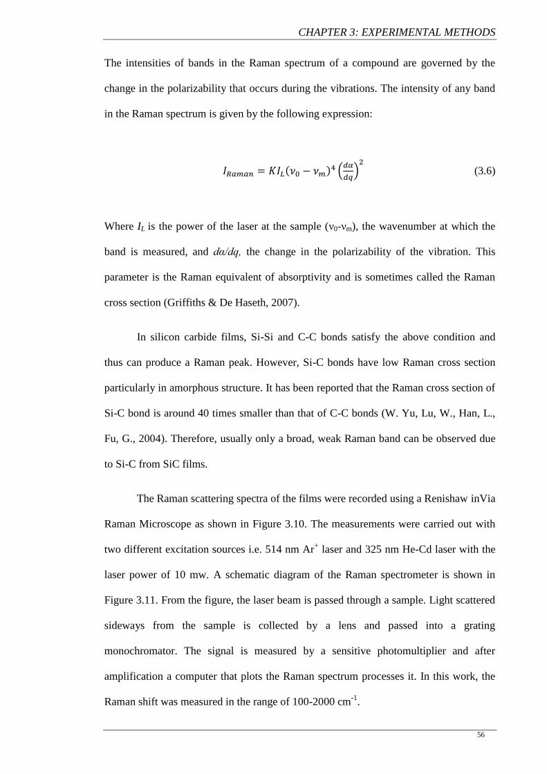
CHAPTER 3: EXPERIMENTAL METHODS
56
The intensities of bands in the Raman spectrum of a compound are governed by the
change in the polarizability that occurs during the vibrations. The intensity of any band
in the Raman spectrum is given by the following expression:
( ) (
)
(3.6)
Where IL is the power of the laser at the sample (ν0-νm), the wavenumber at which the
band is measured, and dα/dq, the change in the polarizability of the vibration. This
parameter is the Raman equivalent of absorptivity and is sometimes called the Raman
cross section (Griffiths & De Haseth, 2007).
In silicon carbide films, Si-Si and C-C bonds satisfy the above condition and
thus can produce a Raman peak. However, Si-C bonds have low Raman cross section
particularly in amorphous structure. It has been reported that the Raman cross section of
Si-C bond is around 40 times smaller than that of C-C bonds (W. Yu, Lu, W., Han, L.,
Fu, G., 2004). Therefore, usually only a broad, weak Raman band can be observed due
to Si-C from SiC films.
The Raman scattering spectra of the films were recorded using a Renishaw inVia
Raman Microscope as shown in Figure 3.10. The measurements were carried out with
two different excitation sources i.e. 514 nm Ar+ laser and 325 nm He-Cd laser with the
laser power of 10 mw. A schematic diagram of the Raman spectrometer is shown in
Figure 3.11. From the figure, the laser beam is passed through a sample. Light scattered
sideways from the sample is collected by a lens and passed into a grating
monochromator. The signal is measured by a sensitive photomultiplier and after
amplification a computer that plots the Raman spectrum processes it. In this work, the
Raman shift was measured in the range of 100-2000 cm-1
.
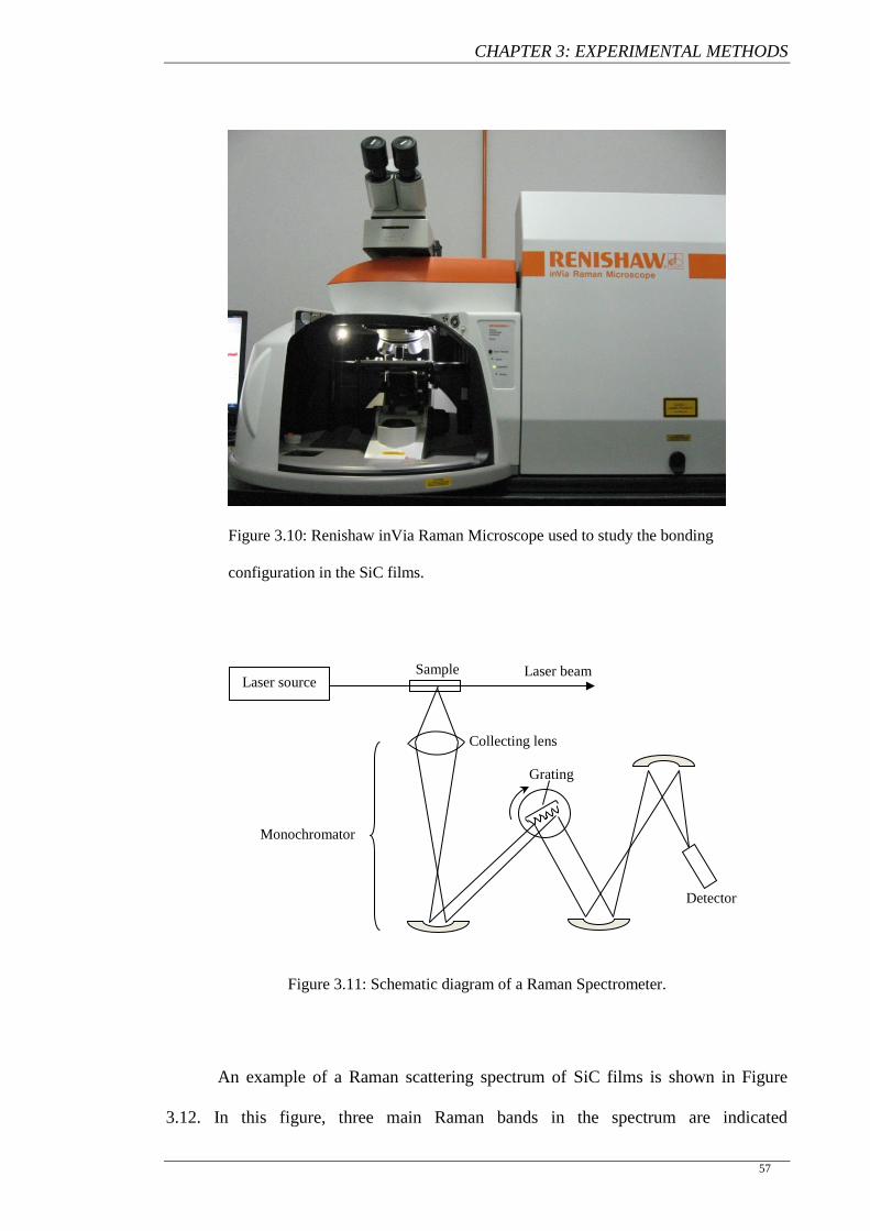
CHAPTER 3: EXPERIMENTAL METHODS
57
Figure 3.10: Renishaw inVia Raman Microscope used to study the bonding
configuration in the SiC films.
Figure 3.11: Schematic diagram of a Raman Spectrometer.
An example of a Raman scattering spectrum of SiC films is shown in Figure
3.12. In this figure, three main Raman bands in the spectrum are indicated
Laser source Laser beam Sample
Detector
Grating
Collecting lens
Monochromator
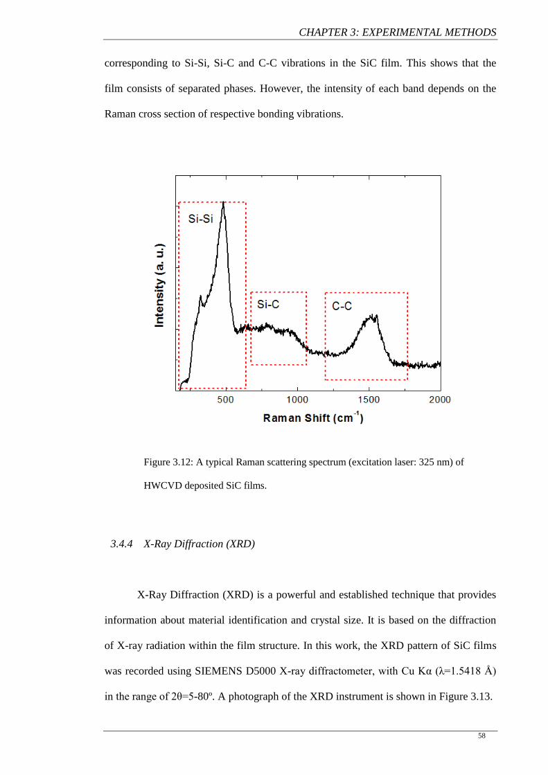
CHAPTER 3: EXPERIMENTAL METHODS
58
corresponding to Si-Si, Si-C and C-C vibrations in the SiC film. This shows that the
film consists of separated phases. However, the intensity of each band depends on the
Raman cross section of respective bonding vibrations.
Figure 3.12: A typical Raman scattering spectrum (excitation laser: 325 nm) of
HWCVD deposited SiC films.
3.4.4 X-Ray Diffraction (XRD)
X-Ray Diffraction (XRD) is a powerful and established technique that provides
information about material identification and crystal size. It is based on the diffraction
of X-ray radiation within the film structure. In this work, the XRD pattern of SiC films
was recorded using SIEMENS D5000 X-ray diffractometer, with Cu Kα (λ=1.5418 Å)
in the range of 2θ=5-80º. A photograph of the XRD instrument is shown in Figure 3.13.
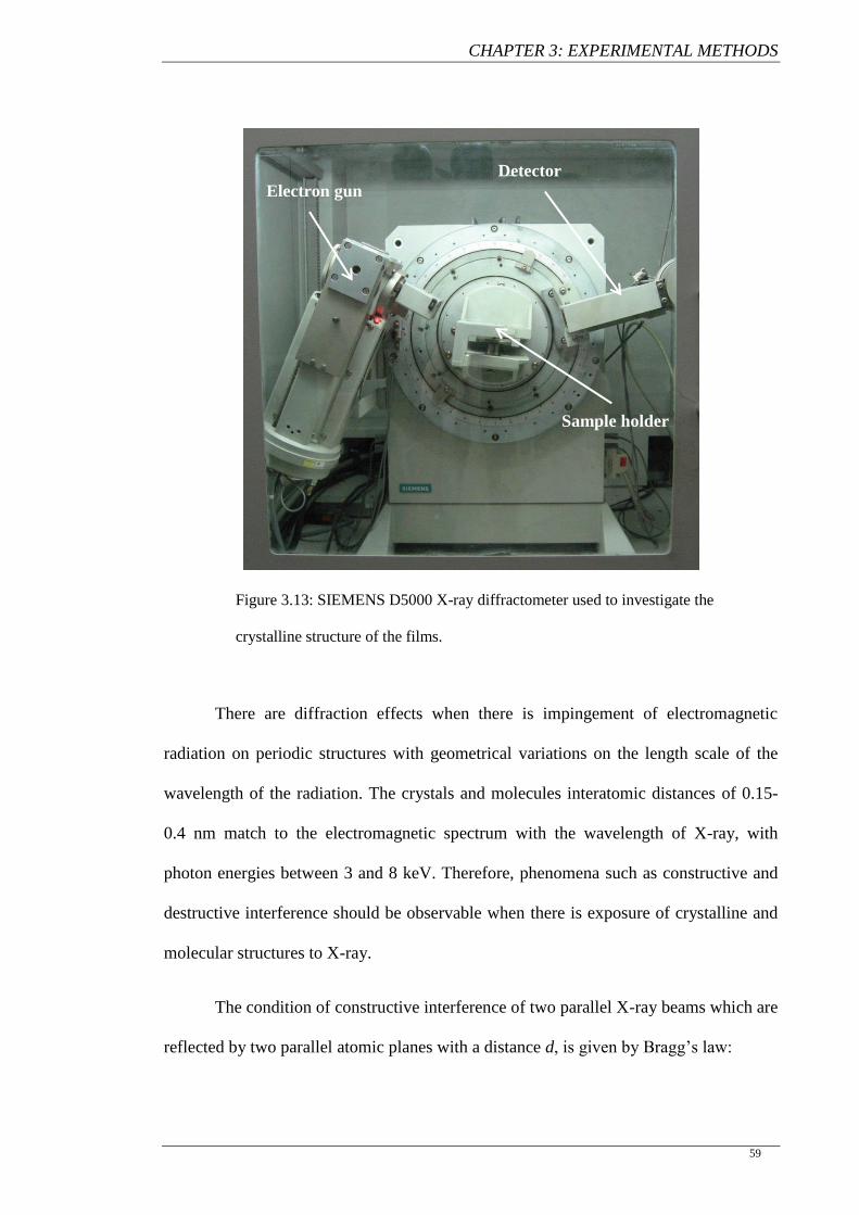
CHAPTER 3: EXPERIMENTAL METHODS
59
Figure 3.13: SIEMENS D5000 X-ray diffractometer used to investigate the
crystalline structure of the films.
There are diffraction effects when there is impingement of electromagnetic
radiation on periodic structures with geometrical variations on the length scale of the
wavelength of the radiation. The crystals and molecules interatomic distances of 0.15-
0.4 nm match to the electromagnetic spectrum with the wavelength of X-ray, with
photon energies between 3 and 8 keV. Therefore, phenomena such as constructive and
destructive interference should be observable when there is exposure of crystalline and
molecular structures to X-ray.
The condition of constructive interference of two parallel X-ray beams which are
reflected by two parallel atomic planes with a distance d, is given by Bragg’s law:
Electron gun
Detector
Sample holder
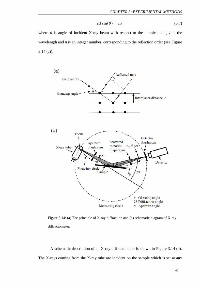
CHAPTER 3: EXPERIMENTAL METHODS
60
( ) (3.7)
where θ is angle of incident X-ray beam with respect to the atomic plane, λ is the
wavelength and n is an integer number, corresponding to the reflection order (see Figure
3.14 (a)).
Figure 3.14: (a) The principle of X-ray diffraction and (b) schematic diagram of X-ray
diffractometer.
A schematic description of an X-ray diffractometer is shown in Figure 3.14 (b).
The X-rays coming from the X-ray tube are incident on the sample which is set at any
CHAPTER 3: EXPERIMENTAL METHODS
61
desired angle to the incident beam. The collection of the diffraction pattern is by
varying the incidence angle of the incoming X-ray beam by θ and the scattering angle
by 2θ while measuring the scattered intensity I(2θ). A real picture of X-ray
diffractometer is shown in Figure 3.13.
If the atoms in a crystal are regularly arranged in a long range, the diffraction
pattern contains sharp interference peaks. The size of crystallites (t) can be determined
from Scherrer formula:
(3.8)
where B is the width at an intensity level equal to half the maximum (FWHM) of the
diffraction peak and θB is the Bragg angle, which is the angle of incident X-ray beam.
From this formula, it is obvious that bigger crystals result in sharper diffraction peaks at
the position of 2θB.
The Bragg condition is not fulfilled in liquids and amorphous solids due to lack
of long range order. The amorphous phase can only produce a broad peak in the
diffraction pattern.
3.4.5 Auger Electron Spectroscopy (AES)
In 1925, Auger observed that an ionized atom could eject another electron
(second ionization) if the first ionization occurs in the inner shell. Because the kinetic
energy of the second ejected electron is dependent on the electronic structure of the
element, it can be used to identify the element from which the electron is ejected. This is
called Auger effect. The ejected electron is known as Auger electron. Based on the
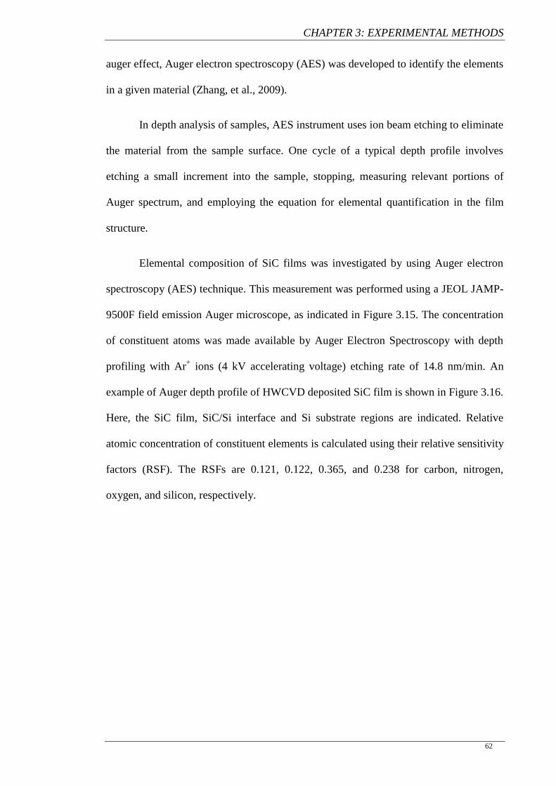
CHAPTER 3: EXPERIMENTAL METHODS
62
auger effect, Auger electron spectroscopy (AES) was developed to identify the elements
in a given material (Zhang, et al., 2009).
In depth analysis of samples, AES instrument uses ion beam etching to eliminate
the material from the sample surface. One cycle of a typical depth profile involves
etching a small increment into the sample, stopping, measuring relevant portions of
Auger spectrum, and employing the equation for elemental quantification in the film
structure.
Elemental composition of SiC films was investigated by using Auger electron
spectroscopy (AES) technique. This measurement was performed using a JEOL JAMP-
9500F field emission Auger microscope, as indicated in Figure 3.15. The concentration
of constituent atoms was made available by Auger Electron Spectroscopy with depth
profiling with Ar+ ions (4 kV accelerating voltage) etching rate of 14.8 nm/min. An
example of Auger depth profile of HWCVD deposited SiC film is shown in Figure 3.16.
Here, the SiC film, SiC/Si interface and Si substrate regions are indicated. Relative
atomic concentration of constituent elements is calculated using their relative sensitivity
factors (RSF). The RSFs are 0.121, 0.122, 0.365, and 0.238 for carbon, nitrogen,
oxygen, and silicon, respectively.
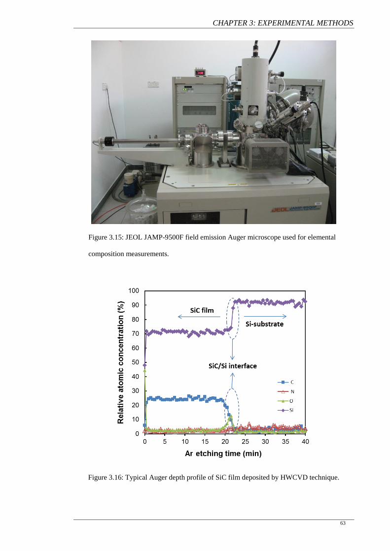
CHAPTER 3: EXPERIMENTAL METHODS
63
Figure 3.15: JEOL JAMP-9500F field emission Auger microscope used for elemental
composition measurements.
Figure 3.16: Typical Auger depth profile of SiC film deposited by HWCVD technique.
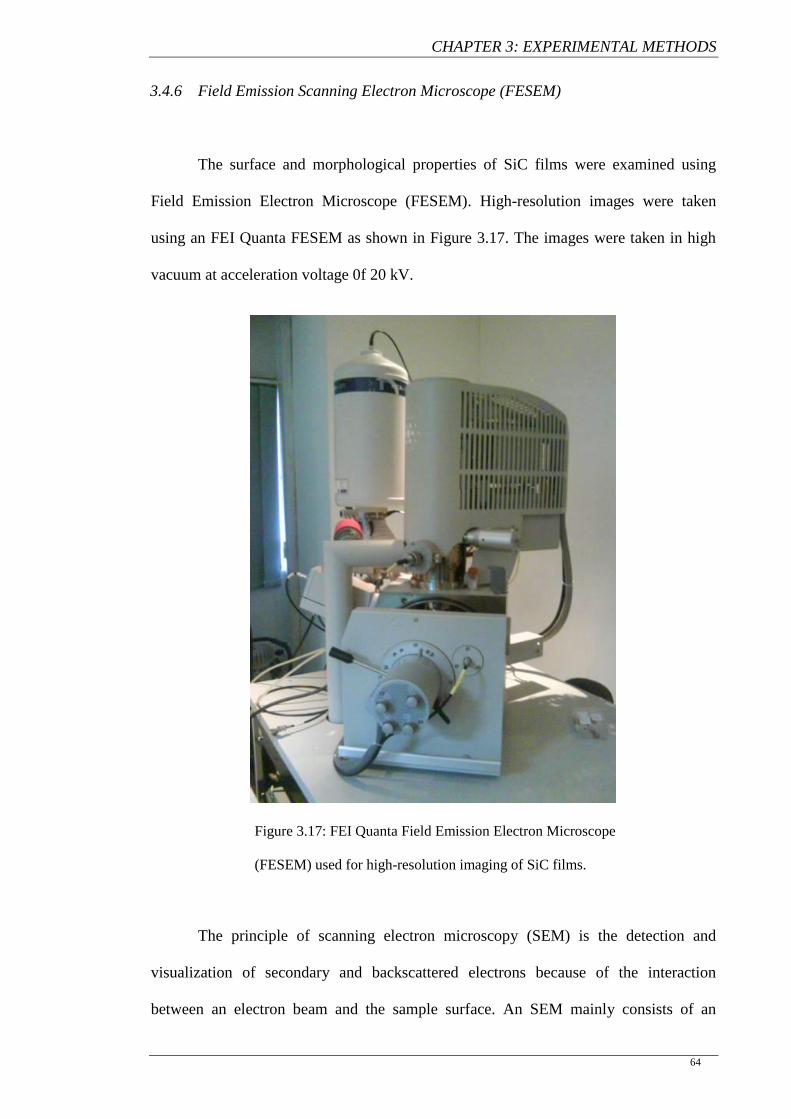
CHAPTER 3: EXPERIMENTAL METHODS
64
3.4.6 Field Emission Scanning Electron Microscope (FESEM)
The surface and morphological properties of SiC films were examined using
Field Emission Electron Microscope (FESEM). High-resolution images were taken
using an FEI Quanta FESEM as shown in Figure 3.17. The images were taken in high
vacuum at acceleration voltage 0f 20 kV.
Figure 3.17: FEI Quanta Field Emission Electron Microscope
(FESEM) used for high-resolution imaging of SiC films.
The principle of scanning electron microscopy (SEM) is the detection and
visualization of secondary and backscattered electrons because of the interaction
between an electron beam and the sample surface. An SEM mainly consists of an
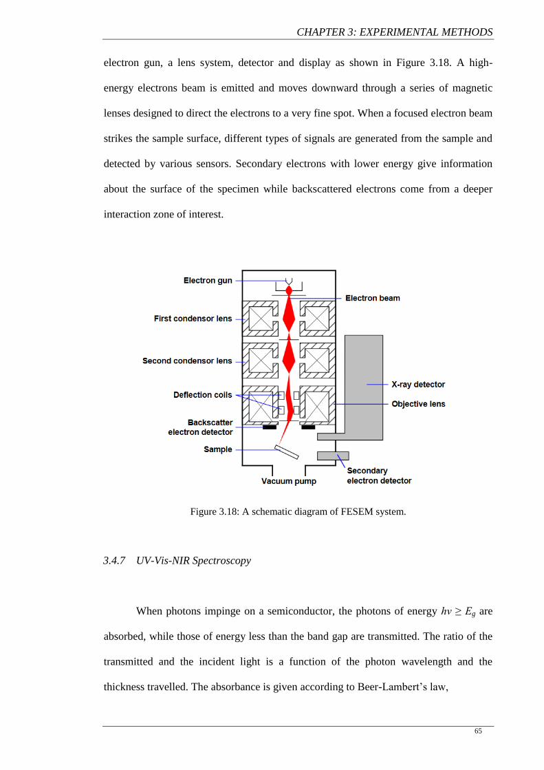
CHAPTER 3: EXPERIMENTAL METHODS
65
electron gun, a lens system, detector and display as shown in Figure 3.18. A high-
energy electrons beam is emitted and moves downward through a series of magnetic
lenses designed to direct the electrons to a very fine spot. When a focused electron beam
strikes the sample surface, different types of signals are generated from the sample and
detected by various sensors. Secondary electrons with lower energy give information
about the surface of the specimen while backscattered electrons come from a deeper
interaction zone of interest.
Figure 3.18: A schematic diagram of FESEM system.
3.4.7 UV-Vis-NIR Spectroscopy
When photons impinge on a semiconductor, the photons of energy hν ≥ Eg are
absorbed, while those of energy less than the band gap are transmitted. The ratio of the
transmitted and the incident light is a function of the photon wavelength and the
thickness travelled. The absorbance is given according to Beer-Lambert’s law,
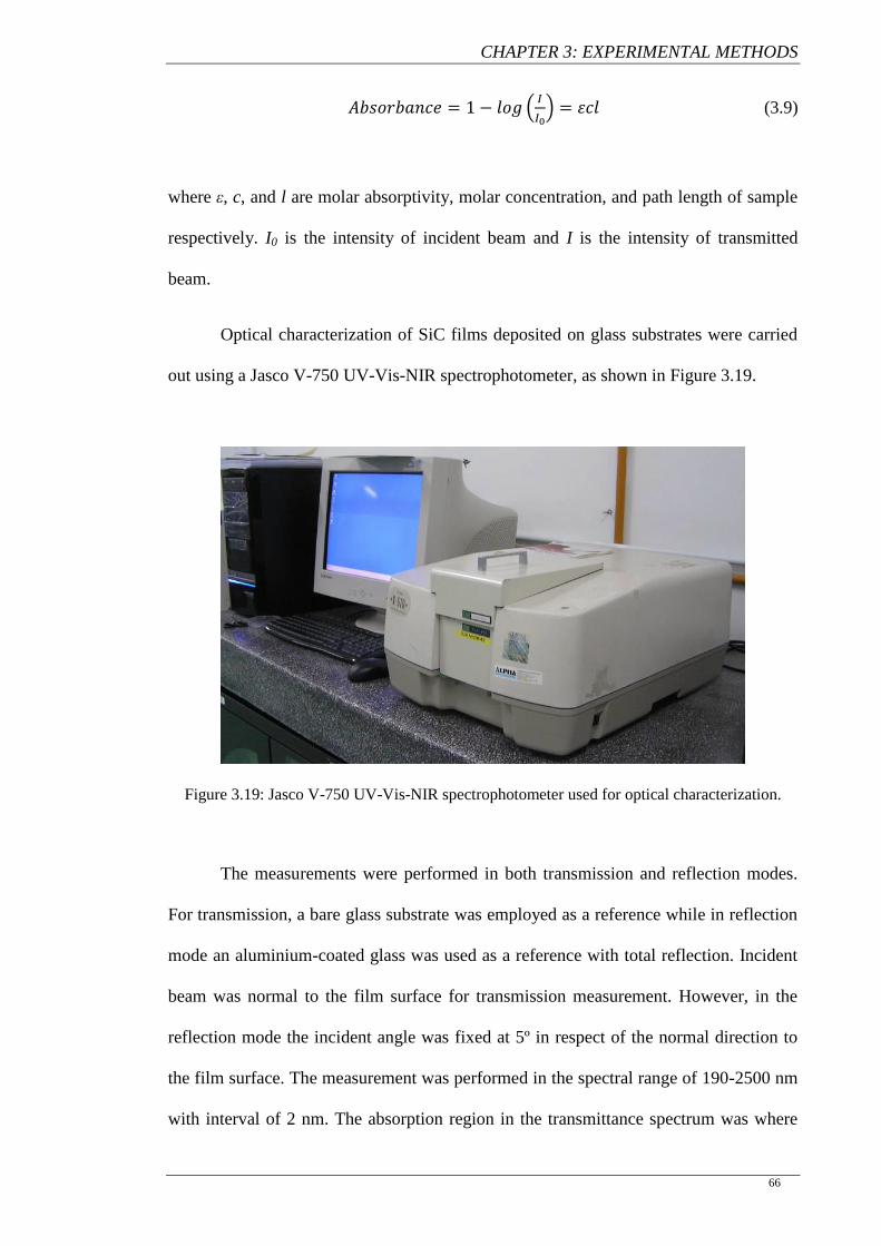
CHAPTER 3: EXPERIMENTAL METHODS
66
(
) (3.9)
where ε, c, and l are molar absorptivity, molar concentration, and path length of sample
respectively. I0 is the intensity of incident beam and I is the intensity of transmitted
beam.
Optical characterization of SiC films deposited on glass substrates were carried
out using a Jasco V-750 UV-Vis-NIR spectrophotometer, as shown in Figure 3.19.
Figure 3.19: Jasco V-750 UV-Vis-NIR spectrophotometer used for optical characterization.
The measurements were performed in both transmission and reflection modes.
For transmission, a bare glass substrate was employed as a reference while in reflection
mode an aluminium-coated glass was used as a reference with total reflection. Incident
beam was normal to the film surface for transmission measurement. However, in the
reflection mode the incident angle was fixed at 5º in respect of the normal direction to
the film surface. The measurement was performed in the spectral range of 190-2500 nm
with interval of 2 nm. The absorption region in the transmittance spectrum was where
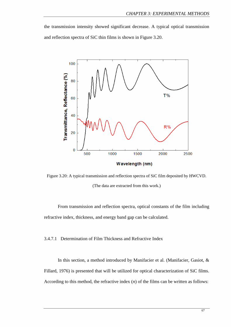
CHAPTER 3: EXPERIMENTAL METHODS
67
the transmission intensity showed significant decrease. A typical optical transmission
and reflection spectra of SiC thin films is shown in Figure 3.20.
Figure 3.20: A typical transmission and reflection spectra of SiC film deposited by HWCVD.
(The data are extracted from this work.)
From transmission and reflection spectra, optical constants of the film including
refractive index, thickness, and energy band gap can be calculated.
3.4.7.1 Determination of Film Thickness and Refractive Index
In this section, a method introduced by Manifacier et al. (Manifacier, Gasiot, &
Fillard, 1976) is presented that will be utilized for optical characterization of SiC films.
According to this method, the refractive index (n) of the films can be written as follows:
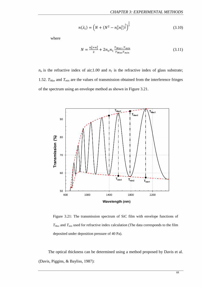
CHAPTER 3: EXPERIMENTAL METHODS
68
( ) ( (
)
)
(3.10)
where
(3.11)
no is the refractive index of air;1.00 and n1 is the refractive index of glass substrate;
1.52. TMax and Tmin are the values of transmission obtained from the interference fringes
of the spectrum using an envelope method as shown in Figure 3.21.
Figure 3.21: The transmission spectrum of SiC film with envelope functions of
TMax and Tmin used for refractive index calculation (The data corresponds to the film
deposited under deposition pressure of 40 Pa).
The optical thickness can be determined using a method proposed by Davis et al.
(Davis, Piggins, & Bayliss, 1987):
CHAPTER 3: EXPERIMENTAL METHODS
69
(3.12)
where m is interference order, λ, n and d, are the wavelength, refractive index and
optical thickness of the corresponding interference order, respectively.
The interference order is taken from the smallest value for the first extreme point
and increases by half for next maximum or minimum point. It should be noted that the
value of m is the integer for maximum points and half integer for minimum points. By
varying the m value for a series of interference fringes, a set of mλ/2 values are
produced which is equal to nd. To determine the m values, a simple graphical method
introduced by Swanepoel et al. (Swanepoel, 1983) is used. If the order number (integer
or half integer) of the first extreme is m1, the equation for the extreme points can be
written as follows:
(
) (3.13)
or
⁄ (3.14)
If k/2 is plotted versus n/λ, the amount of m1 can be obtained from the intercept of the
straight line. By selecting the correct first interference order, the optical thickness (d)
can be simply determined by dividing nd by n at the longest wavelength obtained from
the Manifacier method. The values of the refractive index as a function of wavelength
are then calculated using this thickness. These values must satisfy the Cauchy function:
CHAPTER 3: EXPERIMENTAL METHODS
70
(3.15)
where a and n0′ are linear slope and static refractive index of the film, respectively.
3.4.7.2 Optical Absorption and Band Gap
From the transmission and reflection spectra, the absorption coefficient of the
films can be obtained using the following equation:
(
) (3.16)
where d is the optical thickness of the film as determined following the method
explained in above section. T and R are the transmission and reflection data as obtained
from UV-Vis-NIR measurement.
The energy band gap of SiC films, Eg can be determined from the Tauc relation
(Tauc & Abeles, 1972):
( ) (3.17)
where B is a constant and E is the photon energy. In order to determine the value of Eg,
graph of (αE)1/2
versus photon energy, E, is plotted as an example as shown in Figure
3.22. Extrapolation of the linear part of this plot for (αE)1/2
= 0 gives the value of Eg.
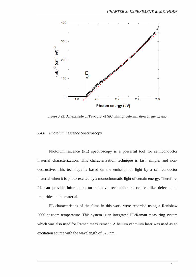
CHAPTER 3: EXPERIMENTAL METHODS
71
Figure 3.22: An example of Tauc plot of SiC film for determination of energy gap.
3.4.8 Photoluminescence Spectroscopy
Photoluminescence (PL) spectroscopy is a powerful tool for semiconductor
material characterization. This characterization technique is fast, simple, and non-
destructive. This technique is based on the emission of light by a semiconductor
material when it is photo-excited by a monochromatic light of certain energy. Therefore,
PL can provide information on radiative recombination centres like defects and
impurities in the material.
PL characteristics of the films in this work were recorded using a Renishaw
2000 at room temperature. This system is an integrated PL/Raman measuring system
which was also used for Raman measurement. A helium cadmium laser was used as an
excitation source with the wavelength of 325 nm.
CHAPTER 4: RESULTS AND DISCUSSION: PART 1
72
CHAPTER 4
Silicon Carbide Thin Films
Prepared by HWCVD Technique
from Pure Silane and Methane:
Part 1
CHAPTER 4: RESULTS AND DISCUSSION: PART 1
73
4.1 Introduction
In this chapter, the deposition of SiC thin films using hot-wire chemical vapour
deposition (HWCVD) from pure silane and methane gas mixture is presented. The
influence of precursor gas concentration on chemical bonding, crystallinity and
elemental composition properties of the films are studied from analysis done on the
Fourier transform infra-red (FTIR), Raman scattering, X-ray diffraction, and Auger
depth profiling measurement of the films deposited on c-Si substrate. Two series of SiC
films were studied in this part. The FTIR transmission spectra were carried out to study
the heteronuclear bonds such as Si-C, Si-H and C-H bonds present in the films. While
Raman scattering spectroscopy was performed to detect the homonuclear bonds i.e. Si-
Si and C-C bonds and carbon bonding configuration. The first series of films consisted
of two sets of films deposited at two different silane flow-rates of 0.5 and 1 sccm while
the flow-rates of methane gas were varied from 10 to 100 sccm in each set. The choice
of SiH4 flow rate was based on earlier reports in the literature that verified ‘silane
starving’ condition is necessary to obtain better quality SiC films (A. A. Kumbhar, et
al., 1998; A. S. Kumbhar, et al., 1995). The second series of films also consisted of
films deposited at different silane (SiH4) and methane (CH4) flow-rates with the gas
flow ratio fixed. Two sets of films were deposited for this series. The films in the first
set were deposited at the deposition pressure of the total gas partial pressure by setting
the rotary pump valve fully opened while the deposition pressure of the second set of
films was fixed by controlling the rotary pump valve. It should be noted that the other
deposition parameters not mentioned above were fixed and will be detailed in the
following section.
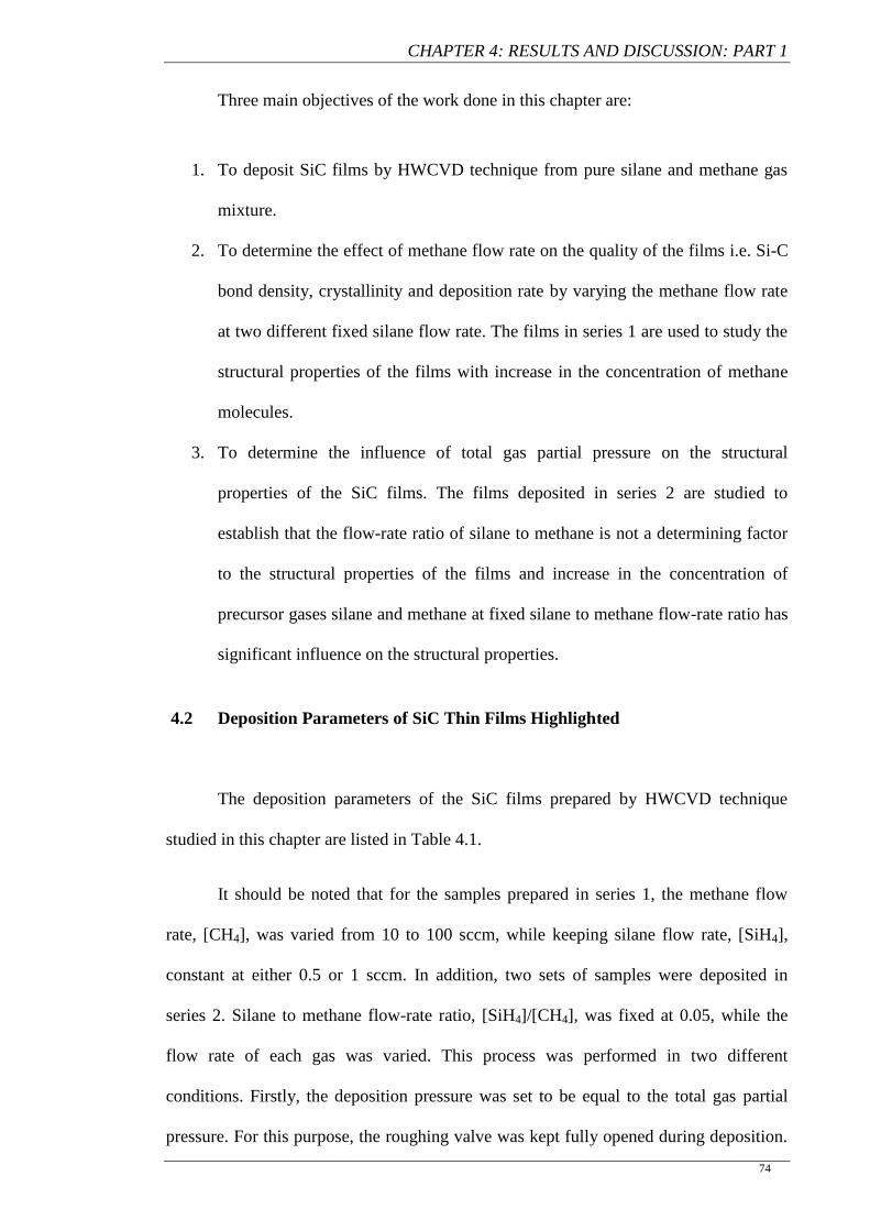
CHAPTER 4: RESULTS AND DISCUSSION: PART 1
74
Three main objectives of the work done in this chapter are:
1. To deposit SiC films by HWCVD technique from pure silane and methane gas
mixture.
2. To determine the effect of methane flow rate on the quality of the films i.e. Si-C
bond density, crystallinity and deposition rate by varying the methane flow rate
at two different fixed silane flow rate. The films in series 1 are used to study the
structural properties of the films with increase in the concentration of methane
molecules.
3. To determine the influence of total gas partial pressure on the structural
properties of the SiC films. The films deposited in series 2 are studied to
establish that the flow-rate ratio of silane to methane is not a determining factor
to the structural properties of the films and increase in the concentration of
precursor gases silane and methane at fixed silane to methane flow-rate ratio has
significant influence on the structural properties.
4.2 Deposition Parameters of SiC Thin Films Highlighted
The deposition parameters of the SiC films prepared by HWCVD technique
studied in this chapter are listed in Table 4.1.
It should be noted that for the samples prepared in series 1, the methane flow
rate, [CH4], was varied from 10 to 100 sccm, while keeping silane flow rate, [SiH4],
constant at either 0.5 or 1 sccm. In addition, two sets of samples were deposited in
series 2. Silane to methane flow-rate ratio, [SiH4]/[CH4], was fixed at 0.05, while the
flow rate of each gas was varied. This process was performed in two different
conditions. Firstly, the deposition pressure was set to be equal to the total gas partial
pressure. For this purpose, the roughing valve was kept fully opened during deposition.
CHAPTER 4: RESULTS AND DISCUSSION: PART 1
75
Therefore, the deposition pressure was a variable parameter. This set of samples is
called “VP” which stands for “Variable Pressure”. For the second set, however, the
deposition pressure was always kept constant at 80 Pa regardless of the
partial pressure. Adjusting the deposition pressure in this set was done by
regulating the roughing valve until the pressure reading is equal to 80 Pa. This set is
named “FP” which stands for “Fixed Pressure”.
Table 4.1: Deposition parameters for SiC films used in this chapter.
Deposition Parameter Value
Filament temperature 1900ºC
Substrate temperature 300°C
Methane flow rate 10-100 sccm (series 1)
10-40 sccm (series 2)
Silane flow rate 1 sccm (series 1, first set)
0.5 sccm (series 1, second set)
0.5-2 sccm (series 2)
Deposition pressure 80 Pa
12-33 Pa (series 2, VP set)
Filament-to-substrate distance 25 mm
Deposition time 30 min
4.3 Deposition of SiC Films Under Fixed Silane Flow-Rate with the Methane
Flow-Rates Varied
4.3.1 Chemical Bonding Investigation by FTIR Spectroscopy
The bonding configurations of the films were studied by FTIR spectroscopy.
Figure 4.1 (a) and (b) show the thickness-normalized FTIR absorption spectra of SiC
films deposited at SiH4 flow rate of 0.5 and 1 sccm, respectively, and indicated CH4
flow rates.
CHAPTER 4: RESULTS AND DISCUSSION: PART 1
76
(a)
(b)
Figure 4.1: FTIR absorption spectra of SiC film deposited under different CH4 flow
rate and SiH4 flow rate of (a) 0.5 sccm and (b) 1 sccm.
CHAPTER 4: RESULTS AND DISCUSSION: PART 1
77
The main feature of these spectra was a sharp and intense absorption band in the
range of 600 cm-1
to 1100 cm-1
. This band is contributed by the superposition of
absorption peaks located at about 650 cm-1
, 800 cm-1
and 980 cm-1
corresponding to the
Si-H wagging (w), Si-C stretching (str) and C-Hn wagging (w) vibration modes,
respectively (Hartel, 2010). Additionally, a weak absorption band in the range of 1900
to 2200 cm-1
was detected which is attributed to Si-H (str) vibration mode (Chew,
2002). C-Hn stretching vibration at the range of 2800-3000 cm-1
(Ritikos, Siong, Ab.
Gani, Muhamad, & Rahman, 2009), usually observed in hydrogenated a-SiC films was
absent in our spectra. It was observed that the former absorption band increased in
intensity with the decrease in CH4 flow rate, while the Si-H (str) band followed the
opposite trend. The decrease in the Si-H (str) intensity indicates a decrease in the
hydrogen concentration in the films prepared at lower CH4 flow rate. Moreover, the
evolution in the shape and width of the Si-C (str) band suggested a phase transformation
from amorphous to crystalline (Kerdiles, 2000; Rajagopalan, 2003) with decrease in
CH4 flow rate. In order to verify this transformation, the standard deconvolutions have
been done for this absorption band. The Si-C (str) band was fitted to both Gaussian and
Lorentzian distribution curves to determine the amorphous and crystalline components
of the SiC phase in the film structure respectively. Many researchers working on SiC
films have widely adopted this technique (Finger et al., 2009; Rajagopalan, 2003; W.
Yu, Wang, X., Lu, W., Wang, S., Bian, Y., Fu, G., 2010). The Lorentzian component of
Si-C (str) mode was dominant in the films deposited at lower CH4 flow rate with
insignificant presence of Si-H (w) and C-H (w) modes. The presence of Gaussian Si-C
(str), Si-H (w) and C-H (w) modes became more significant compared to the Lorentzian
Si-C (str) mode at higher CH4 flow rate. The SiC crystalline volume fraction of the
films prepared at different CH4 flow rate was estimated following the formula
AL/(AG+AL) where AL and AG were the areas under Si-C Lorentzian and Gaussian
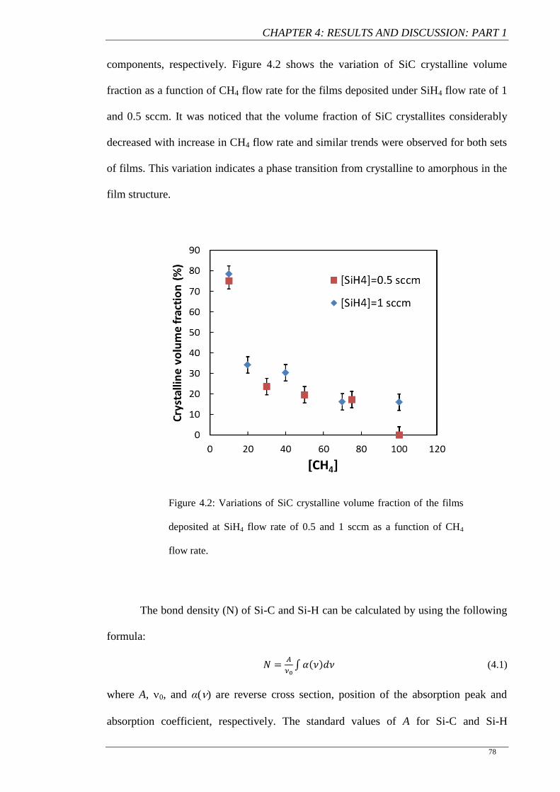
CHAPTER 4: RESULTS AND DISCUSSION: PART 1
78
components, respectively. Figure 4.2 shows the variation of SiC crystalline volume
fraction as a function of CH4 flow rate for the films deposited under SiH4 flow rate of 1
and 0.5 sccm. It was noticed that the volume fraction of SiC crystallites considerably
decreased with increase in CH4 flow rate and similar trends were observed for both sets
of films. This variation indicates a phase transition from crystalline to amorphous in the
film structure.
Figure 4.2: Variations of SiC crystalline volume fraction of the films
deposited at SiH4 flow rate of 0.5 and 1 sccm as a function of CH4
flow rate.
The bond density (N) of Si-C and Si-H can be calculated by using the following
formula:
∫ ( ) (4.1)
where A, 0, and α() are reverse cross section, position of the absorption peak and
absorption coefficient, respectively. The standard values of A for Si-C and Si-H
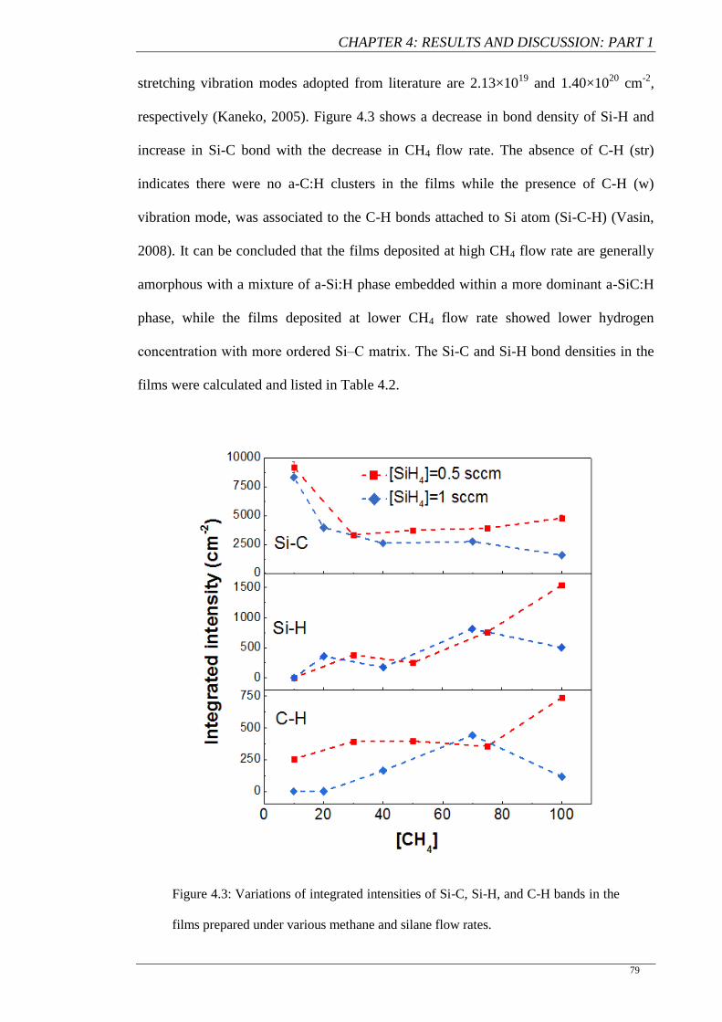
CHAPTER 4: RESULTS AND DISCUSSION: PART 1
79
stretching vibration modes adopted from literature are 2.13×10¹⁹
and 1.40×10²⁰
cm-2
,
respectively (Kaneko, 2005). Figure 4.3 shows a decrease in bond density of Si-H and
increase in Si-C bond with the decrease in CH4 flow rate. The absence of C-H (str)
indicates there were no a-C:H clusters in the films while the presence of C-H (w)
vibration mode, was associated to the C-H bonds attached to Si atom (Si-C-H) (Vasin,
2008). It can be concluded that the films deposited at high CH4 flow rate are generally
amorphous with a mixture of a-Si:H phase embedded within a more dominant a-SiC:H
phase, while the films deposited at lower CH4 flow rate showed lower hydrogen
concentration with more ordered Si‒C matrix. The Si-C and Si-H bond densities in the
films were calculated and listed in Table 4.2.
Figure 4.3: Variations of integrated intensities of Si-C, Si-H, and C-H bands in the
films prepared under various methane and silane flow rates.
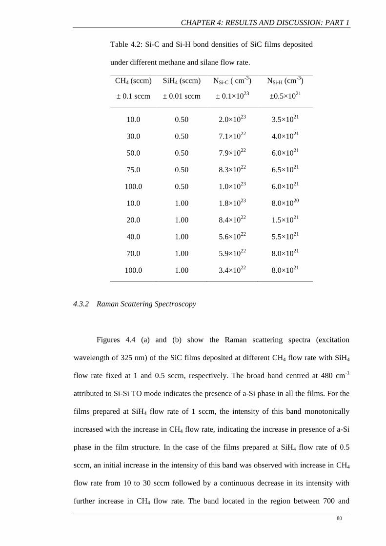
CHAPTER 4: RESULTS AND DISCUSSION: PART 1
80
Table 4.2: Si-C and Si-H bond densities of SiC films deposited
under different methane and silane flow rate.
CH4 (sccm)
± 0.1 sccm
SiH4 (sccm)
± 0.01 sccm
NSi-C ( cm-3
)
± 0.1×10²³
NSi-H (cm-3
)
±0.5×10²¹
10.0 0.50 2.0×10²³
3.5×10²¹
30.0 0.50 7.1×10²²
4.0×10²¹
50.0 0.50 7.9×10²²
6.0×10²¹
75.0 0.50 8.3×10²²
6.5×10²¹
100.0 0.50 1.0×10²³
6.0×10²¹
10.0 1.00 1.8×10²³
8.0×10²⁰
20.0 1.00 8.4×10²²
1.5×10²¹
40.0 1.00 5.6×10²²
5.5×10²¹
70.0 1.00 5.9×10²²
8.0×10²¹
100.0 1.00 3.4×10²²
8.0×10²¹
4.3.2 Raman Scattering Spectroscopy
Figures 4.4 (a) and (b) show the Raman scattering spectra (excitation
wavelength of 325 nm) of the SiC films deposited at different CH4 flow rate with SiH4
flow rate fixed at 1 and 0.5 sccm, respectively. The broad band centred at 480 cm-1
attributed to Si-Si TO mode indicates the presence of a-Si phase in all the films. For the
films prepared at SiH4 flow rate of 1 sccm, the intensity of this band monotonically
increased with the increase in CH4 flow rate, indicating the increase in presence of a-Si
phase in the film structure. In the case of the films prepared at SiH4 flow rate of 0.5
sccm, an initial increase in the intensity of this band was observed with increase in CH4
flow rate from 10 to 30 sccm followed by a continuous decrease in its intensity with
further increase in CH4 flow rate. The band located in the region between 700 and
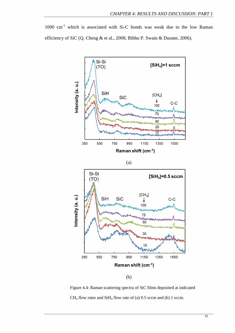
CHAPTER 4: RESULTS AND DISCUSSION: PART 1
81
1000 cm-1
which is associated with Si-C bonds was weak due to the low Raman
efficiency of SiC (Q. Cheng & et al., 2008; Bibhu P. Swain & Dusane, 2006).
(a)
(b)
Figure 4.4: Raman scattering spectra of SiC films deposited at indicated
CH4 flow rates and SiH4 flow rate of (a) 0.5 sccm and (b) 1 sccm.
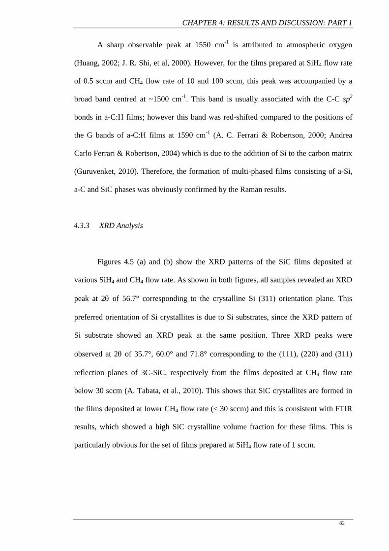
CHAPTER 4: RESULTS AND DISCUSSION: PART 1
82
A sharp observable peak at 1550 cm-1
is attributed to atmospheric oxygen
(Huang, 2002; J. R. Shi, et al, 2000). However, for the films prepared at SiH4 flow rate
of 0.5 sccm and CH4 flow rate of 10 and 100 sccm, this peak was accompanied by a
broad band centred at ~1500 cm-1
. This band is usually associated with the C-C sp2
bonds in a-C:H films; however this band was red-shifted compared to the positions of
the G bands of a-C:H films at 1590 cm-1
(A. C. Ferrari & Robertson, 2000; Andrea
Carlo Ferrari & Robertson, 2004) which is due to the addition of Si to the carbon matrix
(Guruvenket, 2010). Therefore, the formation of multi-phased films consisting of a-Si,
a-C and SiC phases was obviously confirmed by the Raman results.
4.3.3 XRD Analysis
Figures 4.5 (a) and (b) show the XRD patterns of the SiC films deposited at
various SiH4 and CH4 flow rate. As shown in both figures, all samples revealed an XRD
peak at 2 of 56.7° corresponding to the crystalline Si (311) orientation plane. This
preferred orientation of Si crystallites is due to Si substrates, since the XRD pattern of
Si substrate showed an XRD peak at the same position. Three XRD peaks were
observed at 2 of 35.7°, 60.0° and 71.8° corresponding to the (111), (220) and (311)
reflection planes of 3C-SiC, respectively from the films deposited at CH4 flow rate
below 30 sccm (A. Tabata, et al., 2010). This shows that SiC crystallites are formed in
the films deposited at lower CH4 flow rate (< 30 sccm) and this is consistent with FTIR
results, which showed a high SiC crystalline volume fraction for these films. This is
particularly obvious for the set of films prepared at SiH4 flow rate of 1 sccm.
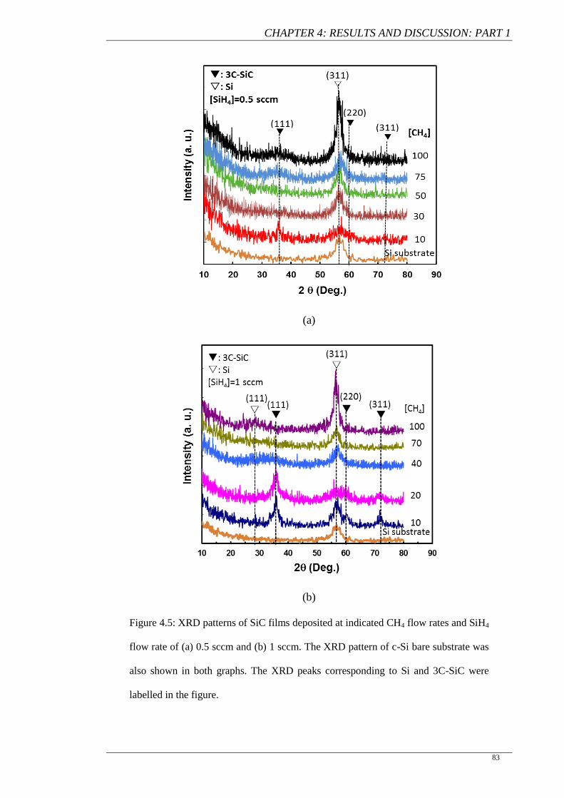
CHAPTER 4: RESULTS AND DISCUSSION: PART 1
83
(a)
(b)
Figure 4.5: XRD patterns of SiC films deposited at indicated CH4 flow rates and SiH4
flow rate of (a) 0.5 sccm and (b) 1 sccm. The XRD pattern of c-Si bare substrate was
also shown in both graphs. The XRD peaks corresponding to Si and 3C-SiC were
labelled in the figure.
CHAPTER 4: RESULTS AND DISCUSSION: PART 1
84
The SiC mean crystallite size of the films estimated from the XRD peak of 3C-SiC
(111) using Scherrer’s formula (Klug & Alexander, 1974), was in the range of 2-6 nm.
The samples prepared at CH4 flow rate above 30 sccm are amorphous. It should be
noted that the films prepared at SiH4 flow rate of 1 and 0.5 sccm, showed the formation
of 3C-SiC nano-crystallites and exhibited high density of Si-C bonds when the CH4
flow rate is 20 sccm and 10 sccm, respectively. The SiH4 to CH4 flow rate ratio for both
of them was the same and equal to 0.05 showing that the formation of SiC crystallites
can be manipulated by controlling the SiH4 to CH4 flow rate ratio.
4.3.4 AES Analysis
The relative atomic concentrations of silicon, Si, and carbon, C, in the films
were obtained from the Auger electron spectroscopy. Figure 4.6 shows the variation of
C/Si ratio with [CH4]/[SiH4] ratio. The inset shows this plot as a function of [CH4].
Since the C/Si appears to show stronger dependence on [CH4]/[SiH4] gas ratio than the
[CH4], the discussion on the results will be focused on the former. The C/Si ratio was
less than 1 in all films indicating that the relative concentration of Si was higher than
that of C in all of the SiC thin films studied in this work. High [SiH4] of 1 sccm resulted
in higher C/Si ratio at each [CH4]/[SiH4] ratio. The increase in [CH4]/[SiH4] ratio up to
100 decreased the C/Si ratio in both set of films. However, further increase in
[CH4]/[SiH4] ratio to 200 which was observed only in the films deposited at [SiH4] of
0.5 sccm for the range of [CH4] studied in this work, intensely increased the C/Si ratio.
These results show that C incorporation into the film structure was strongly influenced
by the partial pressure of CH4 with respect to the SiH4 gas. At [SiH4] of 1 sccm, higher
density of H radicals, generated from decomposition of SiH4 gas by the heated W-
filament, go through the secondary gas-phase reactions with the CH4 molecules and
CHAPTER 4: RESULTS AND DISCUSSION: PART 1
85
enhances the density of C-related radicals reaching the growth sites. This explains the
higher incorporation of C atoms in the films deposited at the [SiH4] of 1 sccm at each
[CH4]/[SiH4] ratio. The increase in [CH4]/[SiH4] ratio decreased the partial pressure of
SiH4 gas and consequently limited the number of Si and H radicals generated during
SiH4 decomposition by the hot filament and thus reduced the density of C-related
radicals reaching the growth sites. Further increase in [CH4]/[SiH4] ratio from 100 to
200 resulted in a significant decrease in Si-related radicals reaching the growth sites.
However, the H radicals produced still contributed to the secondary gas-phase reactions
with CH4 molecules and resulting in the production of C-related radicals. Thus an
increase in C/Si ratio was seen in this region of [CH4]/[SiH4] ratio. The decrease in a-Si
phase in the film as shown by the Raman results with increase in [CH4] for the films
prepared at [SiH4] of 0.5 sccm also confirmed these results.
Figure 4.6: Dependence of carbon to silicon content ratio (C/Si) of
SiC films on CH4 to SiH4 flow rate ratio. The inset displays C/Si
ratio as a function of CH4 flow rate.
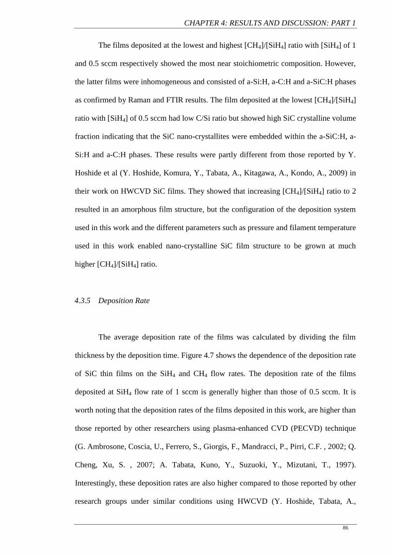
CHAPTER 4: RESULTS AND DISCUSSION: PART 1
86
The films deposited at the lowest and highest [CH4]/[SiH4] ratio with [SiH4] of 1
and 0.5 sccm respectively showed the most near stoichiometric composition. However,
the latter films were inhomogeneous and consisted of a-Si:H, a-C:H and a-SiC:H phases
as confirmed by Raman and FTIR results. The film deposited at the lowest [CH4]/[SiH4]
ratio with [SiH4] of 0.5 sccm had low C/Si ratio but showed high SiC crystalline volume
fraction indicating that the SiC nano-crystallites were embedded within the a-SiC:H, a-
Si:H and a-C:H phases. These results were partly different from those reported by Y.
Hoshide et al (Y. Hoshide, Komura, Y., Tabata, A., Kitagawa, A., Kondo, A., 2009) in
their work on HWCVD SiC films. They showed that increasing [CH4]/[SiH4] ratio to 2
resulted in an amorphous film structure, but the configuration of the deposition system
used in this work and the different parameters such as pressure and filament temperature
used in this work enabled nano-crystalline SiC film structure to be grown at much
higher [CH4]/[SiH4] ratio.
4.3.5 Deposition Rate
The average deposition rate of the films was calculated by dividing the film
thickness by the deposition time. Figure 4.7 shows the dependence of the deposition rate
of SiC thin films on the SiH4 and CH4 flow rates. The deposition rate of the films
deposited at SiH4 flow rate of 1 sccm is generally higher than those of 0.5 sccm. It is
worth noting that the deposition rates of the films deposited in this work, are higher than
those reported by other researchers using plasma-enhanced CVD (PECVD) technique
(G. Ambrosone, Coscia, U., Ferrero, S., Giorgis, F., Mandracci, P., Pirri, C.F. , 2002; Q.
Cheng, Xu, S. , 2007; A. Tabata, Kuno, Y., Suzuoki, Y., Mizutani, T., 1997).
Interestingly, these deposition rates are also higher compared to those reported by other
research groups under similar conditions using HWCVD (Y. Hoshide, Tabata, A.,
CHAPTER 4: RESULTS AND DISCUSSION: PART 1
87
Kitagawa, A., Kondo, A., 2009; Bibhu P. Swain & Dusane, 2006; A. Tabata, et al.,
2009).
It is well known that in HWCVD systems, SiH4 molecules are efficiently
decomposed at the heated W-filament above 1800°C resulting in the generation of high
densities of Si and H radicals (Zheng & Gallagher, 2006). In contrast, although the
decomposition of CH4 molecules may occur in the same way as SiH4, they decompose
mainly via gas phase reactions (A. Tabata & Komura, 2007). An increase in SiH4 flow
rate leads to the production of more Si and H radicals, which in turn, increases the
number of reactions with CH4 molecules and the generation of more C-related radicals.
This enhances the density of the reactive precursors and thus leads to higher film
deposition rate for the films deposited at SiH4 flow rate of 1 sccm.
Figure 4.7: Deposition rate of SiC films deposited at different CH4 flow rate
and SiH4 flow rate of 0.5 and 1 sccm.
CHAPTER 4: RESULTS AND DISCUSSION: PART 1
88
The increase in [CH4] produced similar trends in deposition rates of the films
prepared at [SiH4] of 1 and 0.5 sccm. It increased significantly with initial increase in
[CH4] from 10 to 40 sccm and tended to saturate with further increase in [CH4]. The
films deposited at the lowest [CH4] showed the highest SiC crystalline volume fraction
indicating high coverage of the growth surface with H atoms. The low [CH4] allowed
generation of higher density of Si and H radicals from SiH4 decomposition at the heated
W-filament and enhanced the density of H atoms reaching the growth sites. This also
resulted in more effective etching of the amorphous phase by the H atoms leading to
lowest deposition rate of the films deposited at the lowest [CH4]. Increase in [CH4] from
10 to 40 sccm increased the deposition rate of the films significantly, but further
increase in [CH4] did not produce much change in the deposition rate. It is believed that
the increase in deposition rate with the increase in [CH4] was contributed by a
significant reduction in the density of H radicals reaching the growth sites thus reducing
H etching effects. Although the density of Si and C related radicals reaching the growth
sites was also decreasing, the decrease in H etching effect was more significant as the
density of H radicals was dramatically reduced through gas phase reactions with the
increase in [CH4]. This resulted in the increase in the deposition rate. Similar variation
in the deposition rate had been reported in the region where the structure of SiC phase
transformed from nano-crystalline to amorphous (Komura, 2008), comparable to what
had occurred here. However, when [CH4] increased further beyond 40 sccm, the
significant decrease in the density of H, Si and C-related radicals reaching the growth
surface resulted in an equilibrium state between the growth and etching rate of the films
during the growth process. This contributed to the almost constant deposition rate with
the increase in [CH4] above 40 sccm. These findings show that the [SiH4] is an
important parameter affecting the deposition rate with [CH4] being influential at lower
flow rates.
CHAPTER 4: RESULTS AND DISCUSSION: PART 1
89
4.4 Deposition of SiC Films Under Different Gas Pressures with the Silane to
Methane Flow-Rate Ratio Fixed
4.4.1 Introduction
It is generally known that the deposition pressure and gas flow rate are the two
key parameters controlling the SiC film properties. With regards to gas flow-rate,
researchers generally consider the ratio of gases introduced into the reaction chamber as
an important deposition parameter and put no emphasis on the effects of the actual gas
flow-rates used on the film properties. When considering the effects of deposition
pressure on the film properties, most studies focus on the effects on the film properties
when the gas ratios are fixed with the gas flow-rates fixed and the deposition pressure
changed by controlling the pumping rate evacuating the deposition chamber. In this part
of this work, the effects of varying the reactant gas flow-rates which directly influences
total gas partial pressure at a fixed SiH4 to CH4 flow-rate ratio on the properties of the
films produced are investigated. Thorough literature search done to gather information
on similar work done by other researchers reveals that there is no reported work
available so far covering this aspect. Two sets of samples were deposited for this study.
For the first set of samples (labelled as VP samples), the deposition pressure was fixed
at the lowest stable pressure recorded in the deposition chamber when the reactant gases
were fully admitted. The pumping rate evacuating the reaction chamber was maintained
at the highest rate by fully opening the roughing valve. In other words, the films in this
set were deposited at the same pressure as the total gas partial pressure. For the second
set of films (labelled as FP samples), the deposition pressure was kept constant by
regulating the pumping rate using the roughing valve. As a result, for each total gas
partial pressure, two films deposited at two different deposition pressures were studied.
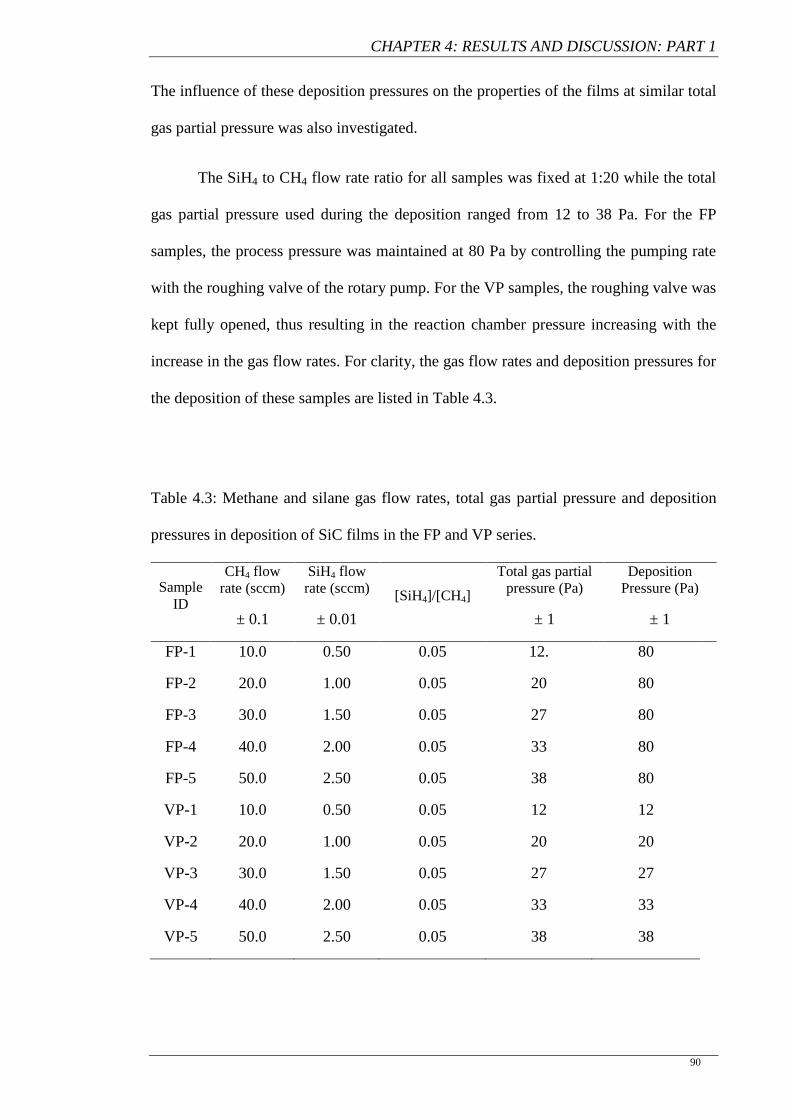
CHAPTER 4: RESULTS AND DISCUSSION: PART 1
90
The influence of these deposition pressures on the properties of the films at similar total
gas partial pressure was also investigated.
The SiH4 to CH4 flow rate ratio for all samples was fixed at 1:20 while the total
gas partial pressure used during the deposition ranged from 12 to 38 Pa. For the FP
samples, the process pressure was maintained at 80 Pa by controlling the pumping rate
with the roughing valve of the rotary pump. For the VP samples, the roughing valve was
kept fully opened, thus resulting in the reaction chamber pressure increasing with the
increase in the gas flow rates. For clarity, the gas flow rates and deposition pressures for
the deposition of these samples are listed in Table 4.3.
Table 4.3: Methane and silane gas flow rates, total gas partial pressure and deposition
pressures in deposition of SiC films in the FP and VP series.
Sample
ID
CH4 flow
rate (sccm)
± 0.1
SiH4 flow
rate (sccm)
± 0.01
[SiH4]/[CH4]
Total gas partial
pressure (Pa)
± 1
Deposition
Pressure (Pa)
± 1
FP-1 10.0 0.50 0.05 12. 80
FP-2 20.0 1.00 0.05 20 80
FP-3 30.0 1.50 0.05 27 80
FP-4 40.0 2.00 0.05 33 80
FP-5 50.0 2.50 0.05 38 80
VP-1 10.0 0.50 0.05 12 12
VP-2 20.0 1.00 0.05 20 20
VP-3 30.0 1.50 0.05 27 27
VP-4 40.0 2.00 0.05 33 33
VP-5 50.0 2.50 0.05 38 38
CHAPTER 4: RESULTS AND DISCUSSION: PART 1
91
4.4.2 Chemical Bonding Investigation by FTIR Spectroscopy
Figures 4.8 (a) and (b) show the FTIR spectra for both the FP and VP samples,
respectively. In the case of the VP samples, VP-1 showed a dominant absorption peak
centered at about 800 cm-1
. The other VP samples showed small absorption peaks
centred at approximately 660, 770, 1000 and 2000 cm-1
correspodning to Si-Hn wagging
modes, Si-C stretching mode, C-Hn wagging mode or Si-O stretching mode and Si-Hn
stretching mode, respectively. The dominant absorption peak produced by VP-1 sample
was actually due to the overlapping of these peaks but the significant presence of SiC
phase in this film resulted in the Si-C stretching band becoming very significant. The
Si-C stretching band appeared to be suppressed when the total gas partial pressure was
increased. The increase in total gas partial pressure with this set of samples also resulted
in an increased presence of Si-O bonds. Increase in the total gas partial pressure above
12 Pa for this set of samples suppressed the formation of Si-C phases and favoured the
formation of a-Si:H and SiO phases in the films.
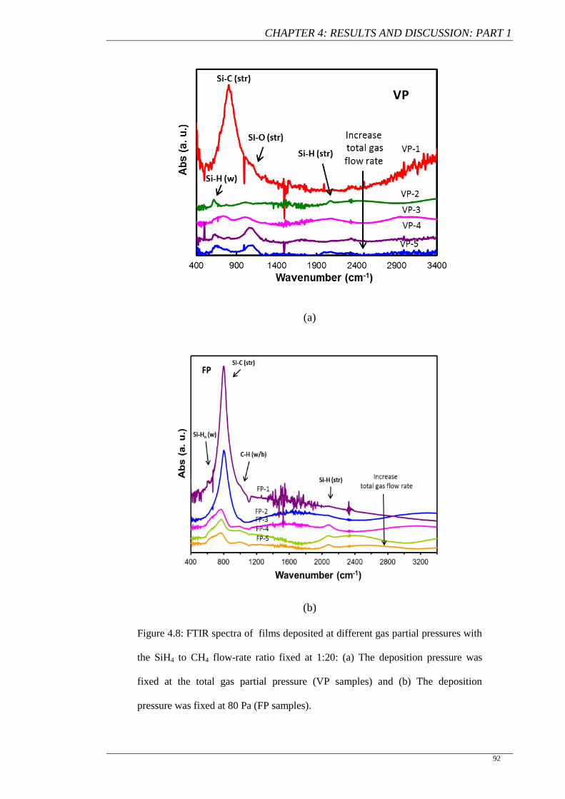
CHAPTER 4: RESULTS AND DISCUSSION: PART 1
92
(a)
(b)
Figure 4.8: FTIR spectra of films deposited at different gas partial pressures with
the SiH4 to CH4 flow-rate ratio fixed at 1:20: (a) The deposition pressure was
fixed at the total gas partial pressure (VP samples) and (b) The deposition
pressure was fixed at 80 Pa (FP samples).
CHAPTER 4: RESULTS AND DISCUSSION: PART 1
93
In the case of FP samples, significant presence of SiC phase was observed in all
the films as indicated by the presence of a dominant peak centred at 800 cm-1
in the
FTIR spectra of these films. This absorption peak centred at 800 cm-1
was sharp and
very intense for the VP-1 and VP-2 films. However, the intensity of this absorption
band significantly decreased and appeared to be red-shifted for the other three films in
this set. This absorption band also broadened for these films transforming from the
Lorentzian to the Gaussian line shape. Additionally, two more absorption bands
associated to Si-H and C-H wagging modes at 660 and 1000 cm-1
, respectively,
appeared in the FTIR spectra of these films. The decrease in the Si-C peak intensity,
red-shift in the peak position, transformation in the line shape from Lorentzian to
Gaussian of the Si-C peak along with the increase in Si-H and C-H bond densities with
increases in the total gas partial pressure for this set of films showed the transformation
of the SiC phase in the films from nano-crystalline to amorphous phase and a relative
increase in the presence of a-C:H and a-Si:H phases with increase in total gas partial
pressure when the pressure in the reaction chamber is fixed at 80 Pa.
Consequently, maintaining the reaction chamber pressure at a higher pressure
than the total gas partial pressure allowed the radicals to have longer residence time in
chamber resulting in higher probability of secondary gas phase reactions. This favoured
the formation of SiC phases in the film structure. However, formation of nano-
crystalline SiC phase in the films was shown to be more favourable at low total gas
partial pressure especially when the pressure in the reaction chamber during the
deposition process was higher than the total gas partial pressure. Increase in the total gas
partial pressure by increasing the SiH4 and CH4 flow-rates keeping the flow-rate ratio
constant only resulted in the suppression in the formation of SiC phases in the film
structure. The increased presence of SiH4 molecules produced more secondary gas
phase reactions of the Si based radicals with these molecules favouring the formation of
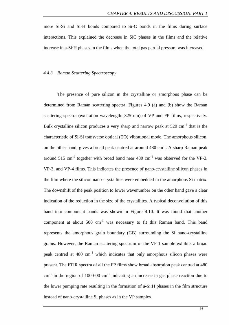
CHAPTER 4: RESULTS AND DISCUSSION: PART 1
94
more Si-Si and Si-H bonds compared to Si-C bonds in the films during surface
interactions. This explained the decrease in SiC phases in the films and the relative
increase in a-Si:H phases in the films when the total gas partial pressure was increased.
4.4.3 Raman Scattering Spectroscopy
The presence of pure silicon in the crystalline or amorphous phase can be
determined from Raman scattering spectra. Figures 4.9 (a) and (b) show the Raman
scattering spectra (excitation wavelength: 325 nm) of VP and FP films, respectively.
Bulk crystalline silicon produces a very sharp and narrow peak at 520 cm-1
that is the
characteristic of Si-Si transverse optical (TO) vibrational mode. The amorphous silicon,
on the other hand, gives a broad peak centred at around 480 cm-1
. A sharp Raman peak
around 515 cm-1
together with broad band near 480 cm-1
was observed for the VP-2,
VP-3, and VP-4 films. This indicates the presence of nano-crystalline silicon phases in
the film where the silicon nano-crystallites were embedded in the amorphous Si matrix.
The downshift of the peak position to lower wavenumber on the other hand gave a clear
indication of the reduction in the size of the crystallites. A typical deconvolution of this
band into component bands was shown in Figure 4.10. It was found that another
component at about 500 cm-1
was necessary to fit this Raman band. This band
represents the amorphous grain boundary (GB) surrounding the Si nano-crystalline
grains. However, the Raman scattering spectrum of the VP-1 sample exhibits a broad
peak centred at 480 cm-1
which indicates that only amorphous silicon phases were
present. The FTIR spectra of all the FP films show broad absorption peak centred at 480
cm-1
in the region of 100-600 cm-1
indicating an increase in gas phase reaction due to
the lower pumping rate resulting in the formation of a-Si:H phases in the film structure
instead of nano-crystalline Si phases as in the VP samples.
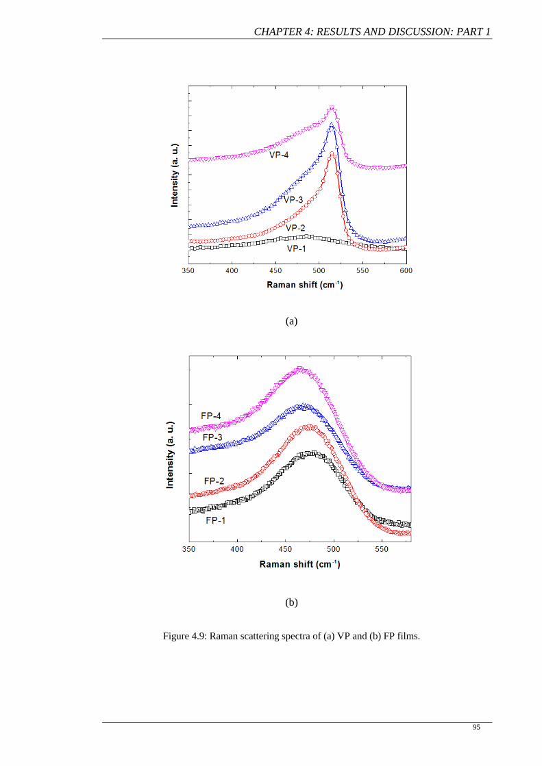
CHAPTER 4: RESULTS AND DISCUSSION: PART 1
95
(a)
(b)
Figure 4.9: Raman scattering spectra of (a) VP and (b) FP films.
CHAPTER 4: RESULTS AND DISCUSSION: PART 1
96
Figure 4.10: Typical deconvolution of Raman spectrum in the ranged of Si-Si vibrations.
In this section, the results show that formation of Si nano-crystals were more
favourable when the films were deposited at the pressure maintained at the total gas
partial pressure (VP samples) and the crystalline Si peak appears to be most dominant
compared to the a-Si peak for the VP-3 sample. The nano-crystalline phase was totally
suppressed in the VP-1 sample suggesting that a reduction in gas phase reactions
reduces the number of energetic H radicals reaching the growth sites resulting in low H
etching effects thus reducing the formation of nano-crystalline Si phases. The decrease
in the nano-crystalline phase present in the VP-4 sample indicates that an increase in
occurrence of collisions during gas phase reactions resulting in less energetic H radicals
reaching the growth sites thus suppressing the formation of nano-crystalline phases.
Therefore, an optimum total gas partial pressure was required in the formation of nano-
crystalline phases in the films.
CHAPTER 4: RESULTS AND DISCUSSION: PART 1
97
4.4.4 XRD Analysis
Figures 4.11 (a) and (b) show the XRD spectra of the SiC films grown at various
total gas partial pressures for VP and FP samples respectively. For the VP samples,
three XRD peaks located at 2 of 28.5°,47.2° and 56.7° assigned to the diffraction peaks
of crystalline Si with orientations of (111), (220), and (311) planes, respectively were
observed. These results confirmed the Raman results that nano-crystalline Si phases
were present in these films although the peak at 56.7° is mainly contributed by the c-Si
substrate as confirmed from the XRD spectrum of the bare Si substrate. The mean
crystallite size estimated from the XRD peak of Si(111) was increased from 3.2 to 5 nm
which indicates an increase in crystallinity of the silicon phases in the film with
increasing total gas partial pressure. Additionally, the film deposited at lowest total gas
partial pressure, VP-1, shows XRD peak at 2 of 35.6° assigned to the diffraction peak
of crystalline cubic silicon carbide with orientation (111) indicating the presence of 3C-
SiC phase in the film structure with orientation of (111). All the FP samples showed a
dominant single Si peak at 56.7° which was believed to be from the c-Si substrate as the
Raman results showed that nano-crystalline phase were not present in these films. The
presence of 3C-SiC phases in the FP-1 and FP-2 samples were also shown from the
XRD spectra of these samples. The presence of 3C-SiC phases in the films deposited at
the lowest total gas partial pressures further confirmed the FTIR results showing that
low total gas partial pressure was more favourable in the formation of crystalline SiC
phases in the film structure and longer residence time of the radicals through increasing
the deposition pressures further enhanced the presence of crystalline SiC phases.
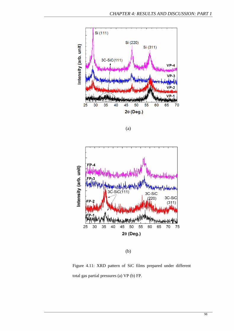
CHAPTER 4: RESULTS AND DISCUSSION: PART 1
98
(a)
(b)
Figure 4.11: XRD pattern of SiC films prepared under different
total gas partial pressures (a) VP (b) FP.
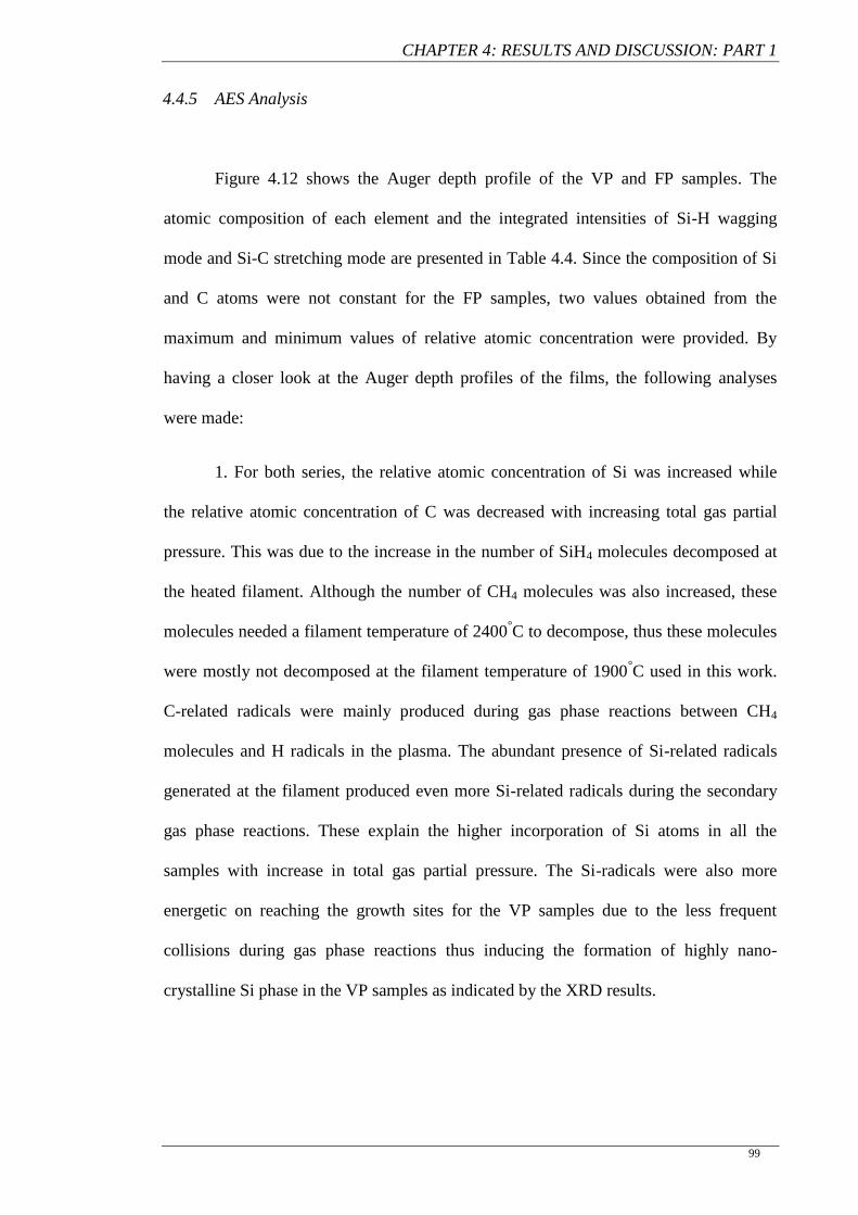
CHAPTER 4: RESULTS AND DISCUSSION: PART 1
99
4.4.5 AES Analysis
Figure 4.12 shows the Auger depth profile of the VP and FP samples. The
atomic composition of each element and the integrated intensities of Si-H wagging
mode and Si-C stretching mode are presented in Table 4.4. Since the composition of Si
and C atoms were not constant for the FP samples, two values obtained from the
maximum and minimum values of relative atomic concentration were provided. By
having a closer look at the Auger depth profiles of the films, the following analyses
were made:
1. For both series, the relative atomic concentration of Si was increased while
the relative atomic concentration of C was decreased with increasing total gas partial
pressure. This was due to the increase in the number of SiH4 molecules decomposed at
the heated filament. Although the number of CH4 molecules was also increased, these
molecules needed a filament temperature of 2400°C to decompose, thus these molecules
were mostly not decomposed at the filament temperature of 1900°C used in this work.
C-related radicals were mainly produced during gas phase reactions between CH4
molecules and H radicals in the plasma. The abundant presence of Si-related radicals
generated at the filament produced even more Si-related radicals during the secondary
gas phase reactions. These explain the higher incorporation of Si atoms in all the
samples with increase in total gas partial pressure. The Si-radicals were also more
energetic on reaching the growth sites for the VP samples due to the less frequent
collisions during gas phase reactions thus inducing the formation of highly nano-
crystalline Si phase in the VP samples as indicated by the XRD results.
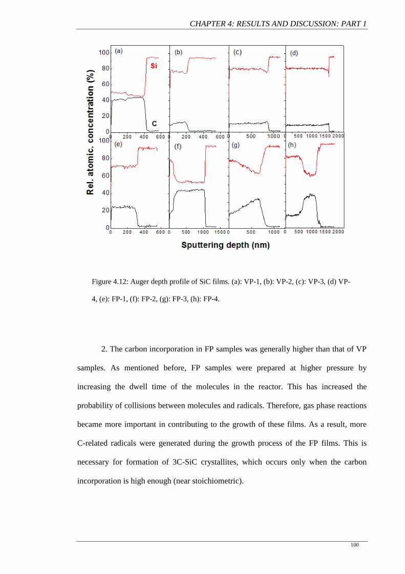
CHAPTER 4: RESULTS AND DISCUSSION: PART 1
100
Figure 4.12: Auger depth profile of SiC films. (a): VP-1, (b): VP-2, (c): VP-3, (d) VP-
4, (e): FP-1, (f): FP-2, (g): FP-3, (h): FP-4.
2. The carbon incorporation in FP samples was generally higher than that of VP
samples. As mentioned before, FP samples were prepared at higher pressure by
increasing the dwell time of the molecules in the reactor. This has increased the
probability of collisions between molecules and radicals. Therefore, gas phase reactions
became more important in contributing to the growth of these films. As a result, more
C-related radicals were generated during the growth process of the FP films. This is
necessary for formation of 3C-SiC crystallites, which occurs only when the carbon
incorporation is high enough (near stoichiometric).
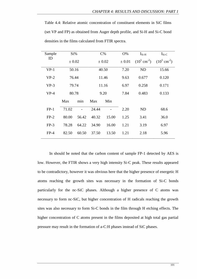
CHAPTER 4: RESULTS AND DISCUSSION: PART 1
101
Table 4.4: Relative atomic concentration of constituent elements in SiC films
(set VP and FP) as obtained from Auger depth profile, and Si-H and Si-C bond
densities in the films calculated from FTIR spectra.
Sample
ID
Si%
± 0.02
C%
± 0.02
O%
± 0.01
ISi-H
(105 cm
-2)
ISi-C
(105 cm
-2)
VP-1 50.16 40.50 7.20 ND 15.66
VP-2 76.44 11.46 9.63 0.677 0.120
VP-3 79.74 11.16 6.97 0.258 0.171
VP-4 80.78 9.20 7.84 0.483 0.133
Max min Max Min
FP-1 71.02 - 24.44 - 2.20 ND 68.6
FP-2 80.00 56.42 40.32 15.00 1.25 3.41 36.0
FP-3 78.28 64.22 34.90 16.00 1.21 3.19 6.97
FP-4 82.50 60.50 37.50 13.50 1.21 2.18 5.96
In should be noted that the carbon content of sample FP-1 detected by AES is
low. However, the FTIR shows a very high intensity Si-C peak. These results appeared
to be contradictory, however it was obvious here that the higher presence of energetic H
atoms reaching the growth sites was necessary in the formation of Si-C bonds
particularly for the nc-SiC phases. Although a higher presence of C atoms was
necessary to form nc-SiC, but higher concentration of H radicals reaching the growth
sites was also necessary to form Si-C bonds in the film through H etching effects. The
higher concentration of C atoms present in the films deposited at high total gas partial
pressure may result in the formation of a-C:H phases instead of SiC phases.
CHAPTER 4: RESULTS AND DISCUSSION: PART 1
102
3. Oxygen contamination detected in the VP samples is about 7-10% that is much
higher than that of FP samples. It has been reported that the surface Si dangling bonds
are easily passivated by oxygen (Goh, 2012; Hartel, 2010). This suggests that during the
deposition of VP samples, many Si dangling bonds were present which passivated by
oxygen atoms in the chamber. Presence of oxygen in these samples is also detected in
the FTIR spectra that show an absorption peak located at 1000-1080 cm-1
that attributed
to stretching mode of Si-O bonds. In contrast, FP samples show negligible oxygen
content which might be due to formation of more hydrogen terminated Si in these
samples that is also supported by FTIR results and by comparing the integrated intensity
of Si-H bonds between FP and VP samples (see Table 4.4).
4. The atomic concentration of Si and C in each of VP samples is almost
constant along its depth but not in FP samples. This is related to different dominant
reactions that took place during deposition. In the process of VP samples deposition, the
gas phase reaction is not very significant because of low pressure and short dwell time
of molecules. Therefore, the most controlling reaction is surface reaction. The radicals
produced by dissociation of SiH4 are very energetic when they reach the substrate
surface. This allows them to continuously find the favourable growth site for growth of
crystalline Si. On the other hand, in the case of FP samples, by increasing the total gas
partial pressure the more Si and H radicals are generated near the heated filament. Then,
they undergo gas phase reactions to decompose the CH4 molecules and produce C-
related radicals. Depth profiles of these samples show that carbon incorporation
increases toward the interface of film and substrate. This means at initial growth of the
film, the C-related radicals react with the surface of substrate and bond to Si atoms.
However, the C-related radicals are not so energetic and they form relatively weak Si-C
bonds. It is known that the sticking coefficient of C-based radicals is lower than that of
Si-based radicals (Q. Cheng & et al., 2008; Q. Cheng, Eugene Tam, Shuyan Xub and
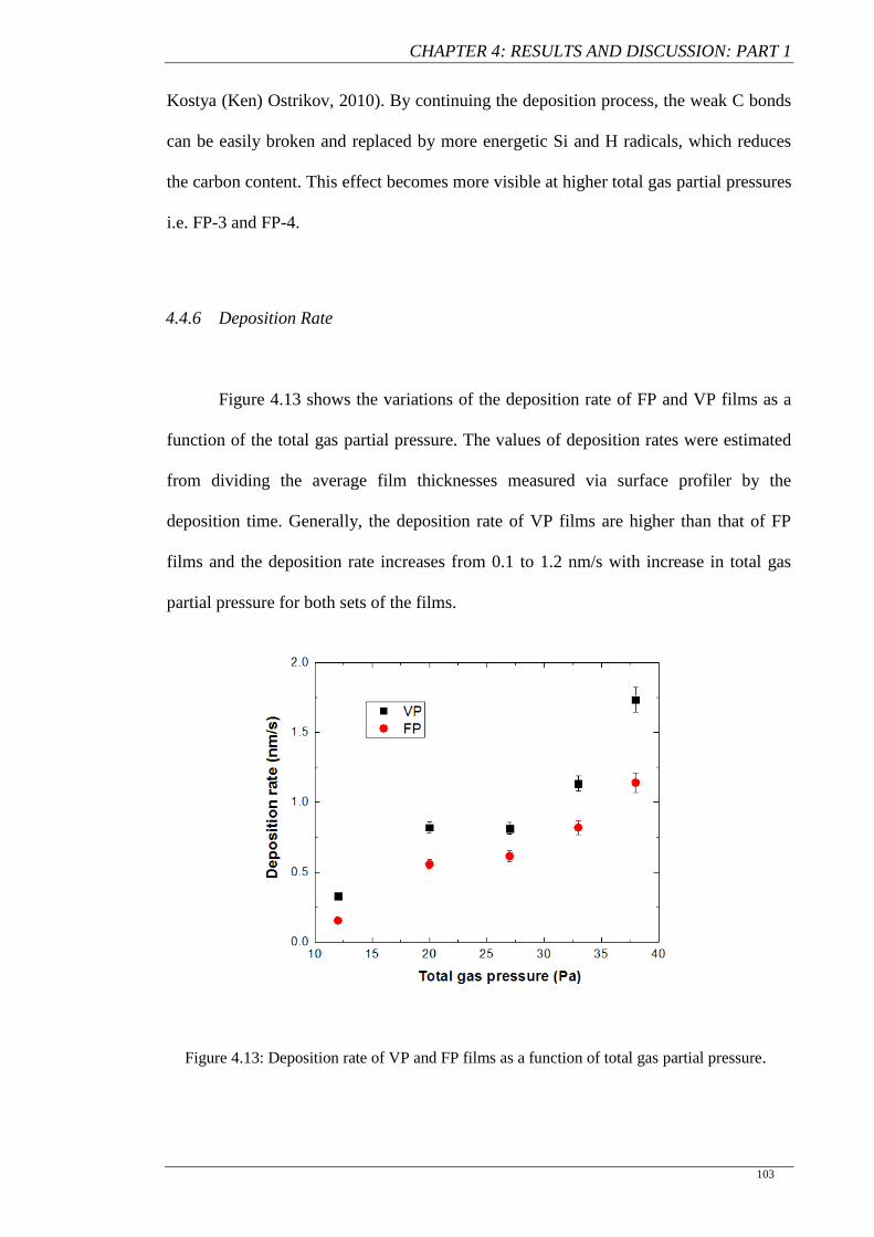
CHAPTER 4: RESULTS AND DISCUSSION: PART 1
103
Kostya (Ken) Ostrikov, 2010). By continuing the deposition process, the weak C bonds
can be easily broken and replaced by more energetic Si and H radicals, which reduces
the carbon content. This effect becomes more visible at higher total gas partial pressures
i.e. FP-3 and FP-4.
4.4.6 Deposition Rate
Figure 4.13 shows the variations of the deposition rate of FP and VP films as a
function of the total gas partial pressure. The values of deposition rates were estimated
from dividing the average film thicknesses measured via surface profiler by the
deposition time. Generally, the deposition rate of VP films are higher than that of FP
films and the deposition rate increases from 0.1 to 1.2 nm/s with increase in total gas
partial pressure for both sets of the films.
Figure 4.13: Deposition rate of VP and FP films as a function of total gas partial pressure.
CHAPTER 4: RESULTS AND DISCUSSION: PART 1
104
The SiC film deposition in HWCVD systems occurs by the decomposition of
silane and methane gas molecules with the hot filament and gas phase reactions. SiH4
molecules are known to be preferentially decomposed on the heated-filament surface
with the temperatures above 1800°C via reaction (2.1) (Gallagher, 2001). CH4
molecules are mainly decomposed through reaction with the H radicals that generated
near the filament resulting from silane dissociation (A. Tabata & Komura, 2007). The
produced Si and C related radicals contributed to the film growth at the surface of
substrate. Therefore, introducing more silane and methane gases, results in more growth
radical production, which enhanced the deposition rate.
In contrast, it was found that applying higher deposition pressure at similar gas
pressures, in contrast, leads to a slight decrease in deposition rate. This was the result of
increment of dwell time of the radicals and molecules due to higher probability of their
collisions with other species on the way to reach the growth surface. The other research
groups have reported similar variations of deposition rate with gas pressure (Komura,
2008; A. Tabata, Kuroda, M., Mori, M., Mizutani, T., Suzuoki, Y., 2004).
4.5 Summary
In this chapter, it has been established that multi-phased SiC thin films can be
deposited using a HWCVD system built in-house for this work from pure silane and
methane gas mixture without hydrogen dilution. The formed films were multi-phased in
structure consisting of a-Si:H, a-C:H, nc-Si:H, a-SiC and nc-SiC phases. The influence
of methane flow rate at fixed silane flow-rates of 0.5 and 1 sccm on the structural,
chemical bonding and elemental composition properties of the films has been
investigated in the first part of the work. In the second part of the work, the influence of
CHAPTER 4: RESULTS AND DISCUSSION: PART 1
105
total gas partial pressure with the silane to methane flow-rate ratio fixed on these
properties was studied at deposition pressure equal to the total gas partial pressure and a
fixed deposition pressure.
An increase in CH4 flow rate with the SiH4 flow-rate fixed at low flow-rate of
0.5 and 1 sccm resulted in a transition from crystalline to amorphous phase of the SiC
phases present in the film structure. The films deposited at high CH4 flow rates are
generally amorphous with a mixture of a-Si:H phase embedded within a more dominant
a-SiC:H phase, while the films deposited at low CH4 flow rates have a more ordered Si-
C matrix with lower hydrogen concentration. SiC crystallites are formed in the films
deposited at low CH4 flow rate. The formation of SiC crystallites can be manipulated by
controlling the CH4 to SiH4 flow rate ratio but this is only possible at low SiH4 flow-
rates not larger than 1 sccm.
Maintaining the reaction chamber pressure at a higher pressure than the total gas
partial pressure has been shown to favour the formation of SiC phases in the film
structure. However, formation of nano-crystalline SiC phase in the films is shown to be
more favourable at low total gas partial pressure especially when the pressure in the
reaction chamber during the deposition process was higher than the total gas partial
pressure. An optimum total gas partial pressure is required for the formation of nano-
crystalline phases in the films. Low total gas partial pressure and longer residence time
of the radicals through increasing the deposition pressures are shown to be more
favourable in the formation of crystalline SiC phases in the film structure.
This work establishes that nano-crystalline SiC film structure can be grown at
much higher CH4 to SiH4 flow-rate ratio and the deposition rates are higher than those
reported by other research groups under similar conditions using HWCVD. The

CHAPTER 4: RESULTS AND DISCUSSION: PART 1
106
deposition mechanism of the films studied in this work has been established through
studying the properties of the films deposited under the different deposition conditions.
CHAPTER 5: RESULTS AND DISCUSSIONS: PART 2
107
CHAPTER 5
Silicon Carbide Thin Films
Prepared by HWCVD Technique
from Pure Silane and Methane:
Part 2
CHAPTER 5: RESULTS AND DISCUSSIONS: PART 2
108
5.1 Introduction
In Chapter 4, the home- built HWCVD system used for this work was shown to
be capable of depositing multi-phased SiC thin films from pure silane and methane gas
mixture without hydrogen dilution. The influence of methane flow rate at fixed silane
flow-rates and total gas partial pressure at fixed silane to methane flow-rate ratio on the
structural, chemical bonding and elemental composition properties of the films was
studied. It was established that nano-crystalline SiC film structure can be grown using
this system at high growth rate. However, the capability of this system to grow films
with higher crystallinity needs to be explored. In this chapter, the influence of
deposition pressure and filament to substrate distance on the structural properties of the
films is studied for this purpose.
Information on the refractive index and optical band gap of SiC films is very
important for applications of the thin films in the optoelectronic devices. The high
refractive index of SiC is very useful in reducing solar cell reflectivity. The wide band
gap of SiC makes it a good candidate for solar cell window layer material. This property
of SiC is also useful for applications in short-wavelength blue and ultraviolet
optoelectronics devices. Therefore, it is very useful to explore the possibility of
controlling the refractive index and band gap of SiC films through identifying the
deposition parameters which can strongly influence these parameters. The correlation
between the structural properties and optical properties of SiC films is important
information that can be utilized to control the refractive index and energy gap of the
films. However, not much work on this aspect of SiC films deposited by HWCVD has
been reported in the literature. Another flaw is that the measurement of refractive index
and band gap energy is usually done on films deposited on transparent substrates like
glass and quartz and characterizations done using FTIR spectroscopy can only be done
CHAPTER 5: RESULTS AND DISCUSSIONS: PART 2
109
on films grown on c-Si substrates. Therefore, valuable information giving accurate
correlation between these properties derived from optical transmission spectroscopy
measurements cannot be obtained. The objectives of this work presented in this chapter
as outlined below are to address these issues. The objectives are
1. To investigate the influence of deposition pressure and substrate to filament
distance on the growth rate, structural and optical properties of SiC films
prepared by HWCVD.
2. To identify the structural properties, which control the refractive index and
band gap energy of the SiC films.
3. To correlate the optical properties to the structural properties of the SiC films.
4. To show that the structural properties of SiC films deposited by the home-built
HWCVD from silane and methane discharge are not substrate dependent.
5.1 Deposition Parameters of SiC Thin Films
Two series of SiC films were deposited under five deposition pressures and four
filament-to-substrate distances. Details on the deposition parameters used during the
deposition of these series of films are tabulated in Tables 5.1 and 5.2. The deposition
pressures are adjusted by controlling the opening of the roughing valve between the
rotary pump and the deposition chamber. The SiH4 and CH4 flow-rates are fixed at 1
and 20 sccm respectively since these were the best flow-rates for these gases for
obtaining SiC nano-crystalline phases in the films as shown by the results in Chapter 4.
The substrate temperature is fixed at 300°C as done in Chapter 4 since this temperature
is the highest temperature that contamination effects from the heating of the Viton O-
rings in the system are minimized. The filament temperature of 1900°C is used because
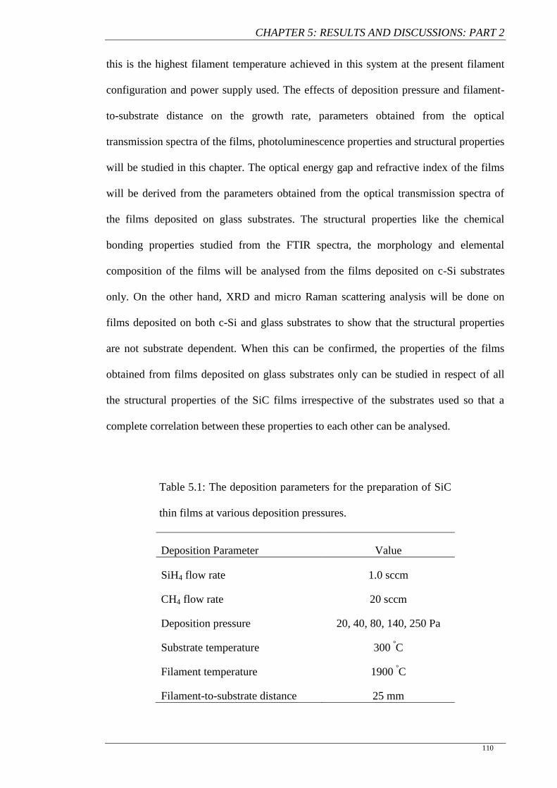
CHAPTER 5: RESULTS AND DISCUSSIONS: PART 2
110
this is the highest filament temperature achieved in this system at the present filament
configuration and power supply used. The effects of deposition pressure and filament-
to-substrate distance on the growth rate, parameters obtained from the optical
transmission spectra of the films, photoluminescence properties and structural properties
will be studied in this chapter. The optical energy gap and refractive index of the films
will be derived from the parameters obtained from the optical transmission spectra of
the films deposited on glass substrates. The structural properties like the chemical
bonding properties studied from the FTIR spectra, the morphology and elemental
composition of the films will be analysed from the films deposited on c-Si substrates
only. On the other hand, XRD and micro Raman scattering analysis will be done on
films deposited on both c-Si and glass substrates to show that the structural properties
are not substrate dependent. When this can be confirmed, the properties of the films
obtained from films deposited on glass substrates only can be studied in respect of all
the structural properties of the SiC films irrespective of the substrates used so that a
complete correlation between these properties to each other can be analysed.
Table 5.1: The deposition parameters for the preparation of SiC
thin films at various deposition pressures.
Deposition Parameter Value
SiH4 flow rate 1.0 sccm
CH4 flow rate 20 sccm
Deposition pressure 20, 40, 80, 140, 250 Pa
Substrate temperature 300 ºC
Filament temperature 1900 ºC
Filament-to-substrate distance 25 mm
CHAPTER 5: RESULTS AND DISCUSSIONS: PART 2
111
Table 5.2: The deposition parameters for the preparation of SiC
thin films at different filament-to-substrate distances.
Deposition Parameter Value
SiH4 flow rate 1.0 sccm
CH4 flow rate 20 sccm
Deposition pressure 80 Pa
Substrate temperature 300 ºC
Filament temperature 1900 ºC
Filament-to-substrate distance 10, 15, 20, 25 mm
5.2 Influence of the Deposition Pressure on the Properties of SiC Films
5.2.1 FTIR Spectroscopy Analysis of SiC Films Deposited on c-Si Substrate
The bonding configurations present in the films were studied by FTIR
spectroscopy. Figure 5.1 shows the thickness-normalized FTIR absorption spectra of
SiC films grown at different deposition pressures.
The main features observed in the spectra of the SiC films studied in Chapter 4
are also observed. The absorption peaks detected from the films include the Si-H
wagging mode (w) at 650 cm-1
, Si-C stretching mode (str) at 800 cm-1
, C-H (W) at 980
cm-1
, Si-CH3 (w) at 1250 cm-1
, Si-H (str) at 2080 cm-1
, and C-Hn (str) at 2800 - 3000
cm-1
.
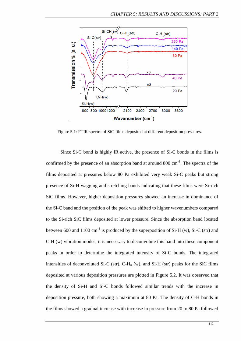
CHAPTER 5: RESULTS AND DISCUSSIONS: PART 2
112
`
Figure 5.1: FTIR spectra of SiC films deposited at different deposition pressures.
Since Si-C bond is highly IR active, the presence of Si-C bonds in the films is
confirmed by the presence of an absorption band at around 800 cm-1
. The spectra of the
films deposited at pressures below 80 Pa exhibited very weak Si-C peaks but strong
presence of Si-H wagging and stretching bands indicating that these films were Si-rich
SiC films. However, higher deposition pressures showed an increase in dominance of
the Si-C band and the position of the peak was shifted to higher wavenumbers compared
to the Si-rich SiC films deposited at lower pressure. Since the absorption band located
between 600 and 1100 cm-1
is produced by the superposition of Si-H (w), Si-C (str) and
C-H (w) vibration modes, it is necessary to deconvolute this band into these component
peaks in order to determine the integrated intensity of Si-C bonds. The integrated
intensities of deconvoluted Si-C (str), C-Hn (w), and Si-H (str) peaks for the SiC films
deposited at various deposition pressures are plotted in Figure 5.2. It was observed that
the density of Si-H and Si-C bonds followed similar trends with the increase in
deposition pressure, both showing a maximum at 80 Pa. The density of C-H bonds in
the films showed a gradual increase with increase in pressure from 20 to 80 Pa followed
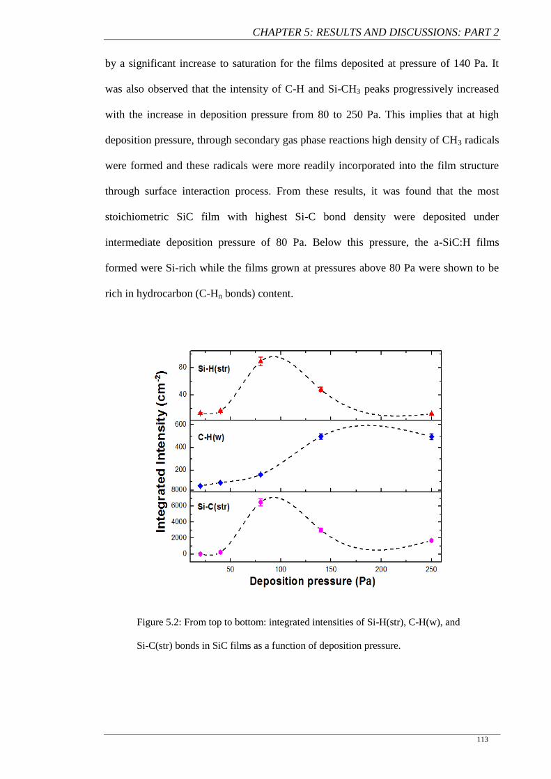
CHAPTER 5: RESULTS AND DISCUSSIONS: PART 2
113
by a significant increase to saturation for the films deposited at pressure of 140 Pa. It
was also observed that the intensity of C-H and Si-CH3 peaks progressively increased
with the increase in deposition pressure from 80 to 250 Pa. This implies that at high
deposition pressure, through secondary gas phase reactions high density of CH3 radicals
were formed and these radicals were more readily incorporated into the film structure
through surface interaction process. From these results, it was found that the most
stoichiometric SiC film with highest Si-C bond density were deposited under
intermediate deposition pressure of 80 Pa. Below this pressure, the a-SiC:H films
formed were Si-rich while the films grown at pressures above 80 Pa were shown to be
rich in hydrocarbon (C-Hn bonds) content.
Figure 5.2: From top to bottom: integrated intensities of Si-H(str), C-H(w), and
Si-C(str) bonds in SiC films as a function of deposition pressure.
CHAPTER 5: RESULTS AND DISCUSSIONS: PART 2
114
5.2.2 Raman Scattering Spectroscopy Analysis of SiC Films Deposited on c-Si and
Glass Substrates
As Si-Si and C-C bonds do not have dipole moment, therefore these bonds
cannot be detected in FTIR spectra of the films. Raman scattering spectroscopy is a
powerful tool to investigate these phases. Figure 5.3 shows Raman scattering spectra
(excitation laser: 325 nm) of SiC films deposited under different deposition pressures.
The various observed bands of intrinsic vibrations were appropriately labelled in the
figure. The films deposited at 20 and 40 Pa exhibited a sharp peak at 518 cm-1
suggesting the presence of Si nano-crystalline phases or clusters in the film structure. At
higher pressure, the sharp peak at 518 cm-1
disappeared and was replaced by the
appearance of a broad peak at 480 cm-1
. This peak corresponded to the amorphous Si
component suggesting that high deposition pressure was more favourable for the
formation of amorphous Si phases in the film structure. The peak corresponds to Si-C
bonds (~ 800 cm-1
) was weak due to lower cross section of Si-C bond compared to those
of Si-Si and C-C bonds (Racine et al., 2001).
The presence of a broad band in the range of 1400-1600 cm-1
shown by the
spectra of the film prepared at 80 Pa indicates the presence of C-C bonds in the a-C:H
clusters within the SiC matrix (Kerdiles et al., 2000). However, this band was not
observed in the spectra of the other films.
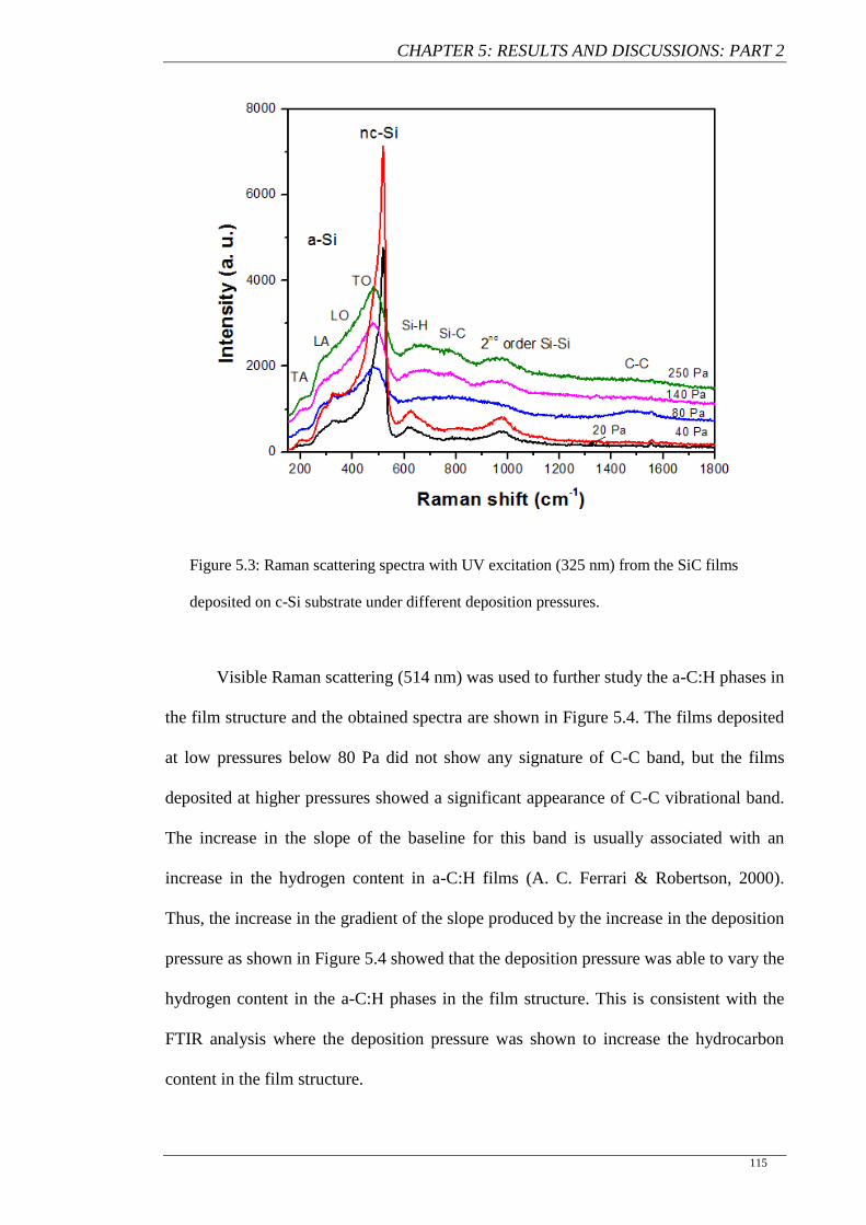
CHAPTER 5: RESULTS AND DISCUSSIONS: PART 2
115
Figure 5.3: Raman scattering spectra with UV excitation (325 nm) from the SiC films
deposited on c-Si substrate under different deposition pressures.
Visible Raman scattering (514 nm) was used to further study the a-C:H phases in
the film structure and the obtained spectra are shown in Figure 5.4. The films deposited
at low pressures below 80 Pa did not show any signature of C-C band, but the films
deposited at higher pressures showed a significant appearance of C-C vibrational band.
The increase in the slope of the baseline for this band is usually associated with an
increase in the hydrogen content in a-C:H films (A. C. Ferrari & Robertson, 2000).
Thus, the increase in the gradient of the slope produced by the increase in the deposition
pressure as shown in Figure 5.4 showed that the deposition pressure was able to vary the
hydrogen content in the a-C:H phases in the film structure. This is consistent with the
FTIR analysis where the deposition pressure was shown to increase the hydrocarbon
content in the film structure.
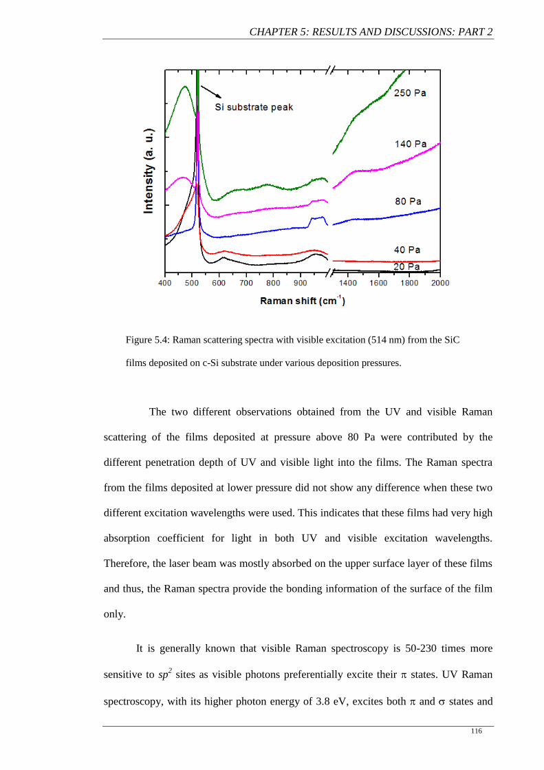
CHAPTER 5: RESULTS AND DISCUSSIONS: PART 2
116
Figure 5.4: Raman scattering spectra with visible excitation (514 nm) from the SiC
films deposited on c-Si substrate under various deposition pressures.
The two different observations obtained from the UV and visible Raman
scattering of the films deposited at pressure above 80 Pa were contributed by the
different penetration depth of UV and visible light into the films. The Raman spectra
from the films deposited at lower pressure did not show any difference when these two
different excitation wavelengths were used. This indicates that these films had very high
absorption coefficient for light in both UV and visible excitation wavelengths.
Therefore, the laser beam was mostly absorbed on the upper surface layer of these films
and thus, the Raman spectra provide the bonding information of the surface of the film
only.
It is generally known that visible Raman spectroscopy is 50-230 times more
sensitive to sp2 sites as visible photons preferentially excite their states. UV Raman
spectroscopy, with its higher photon energy of 3.8 eV, excites both and states and
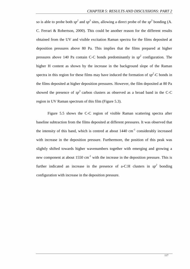
CHAPTER 5: RESULTS AND DISCUSSIONS: PART 2
117
so is able to probe both sp2 and sp
3 sites, allowing a direct probe of the sp
3 bonding (A.
C. Ferrari & Robertson, 2000). This could be another reason for the different results
obtained from the UV and visible excitation Raman spectra for the films deposited at
deposition pressures above 80 Pa. This implies that the films prepared at higher
pressures above 140 Pa contain C-C bonds predominantly in sp2 configuration. The
higher H content as shown by the increase in the background slope of the Raman
spectra in this region for these films may have induced the formation of sp2-C bonds in
the films deposited at higher deposition pressures. However, the film deposited at 80 Pa
showed the presence of sp3
carbon clusters as observed as a broad band in the C-C
region in UV Raman spectrum of this film (Figure 5.3).
Figure 5.5 shows the C-C region of visible Raman scattering spectra after
baseline subtraction from the films deposited at different pressures. It was observed that
the intensity of this band, which is centred at about 1440 cm-1
considerably increased
with increase in the deposition pressure. Furthermore, the position of this peak was
slightly shifted towards higher wavenumbers together with emerging and growing a
new component at about 1550 cm-1
with the increase in the deposition pressure. This is
further indicated an increase in the presence of a-C:H clusters in sp2 bonding
configuration with increase in the deposition pressure.
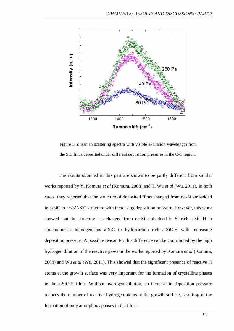
CHAPTER 5: RESULTS AND DISCUSSIONS: PART 2
118
Figure 5.5: Raman scattering spectra with visible excitation wavelength from
the SiC films deposited under different deposition pressures in the C-C region.
The results obtained in this part are shown to be partly different from similar
works reported by Y. Komura et al (Komura, 2008) and T. Wu et al (Wu, 2011). In both
cases, they reported that the structure of deposited films changed from nc-Si embedded
in a-SiC to nc-3C-SiC structure with increasing deposition pressure. However, this work
showed that the structure has changed from nc-Si embedded in Si rich a-SiC:H to
stoichiometric homogeneous a-SiC to hydrocarbon rich a-SiC:H with increasing
deposition pressure. A possible reason for this difference can be contributed by the high
hydrogen dilution of the reactive gases in the works reported by Komura et al (Komura,
2008) and Wu et al (Wu, 2011). This showed that the significant presence of reactive H
atoms at the growth surface was very important for the formation of crystalline phases
in the a-SiC:H films. Without hydrogen dilution, an increase in deposition pressure
reduces the number of reactive hydrogen atoms at the growth surface, resulting in the
formation of only amorphous phases in the films.
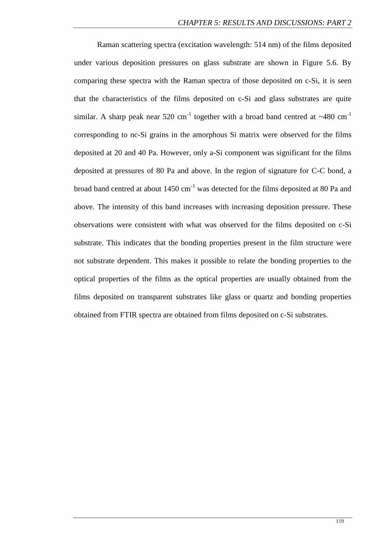
CHAPTER 5: RESULTS AND DISCUSSIONS: PART 2
119
Raman scattering spectra (excitation wavelength: 514 nm) of the films deposited
under various deposition pressures on glass substrate are shown in Figure 5.6. By
comparing these spectra with the Raman spectra of those deposited on c-Si, it is seen
that the characteristics of the films deposited on c-Si and glass substrates are quite
similar. A sharp peak near 520 cm-1
together with a broad band centred at ~480 cm-1
corresponding to nc-Si grains in the amorphous Si matrix were observed for the films
deposited at 20 and 40 Pa. However, only a-Si component was significant for the films
deposited at pressures of 80 Pa and above. In the region of signature for C-C bond, a
broad band centred at about 1450 cm-1
was detected for the films deposited at 80 Pa and
above. The intensity of this band increases with increasing deposition pressure. These
observations were consistent with what was observed for the films deposited on c-Si
substrate. This indicates that the bonding properties present in the film structure were
not substrate dependent. This makes it possible to relate the bonding properties to the
optical properties of the films as the optical properties are usually obtained from the
films deposited on transparent substrates like glass or quartz and bonding properties
obtained from FTIR spectra are obtained from films deposited on c-Si substrates.
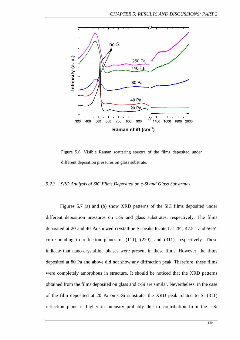
CHAPTER 5: RESULTS AND DISCUSSIONS: PART 2
120
Figure 5.6. Visible Raman scattering spectra of the films deposited under
different deposition pressures on glass substrate.
5.2.3 XRD Analysis of SiC Films Deposited on c-Si and Glass Substrates
Figures 5.7 (a) and (b) show XRD patterns of the SiC films deposited under
different deposition pressures on c-Si and glass substrates, respectively. The films
deposited at 20 and 40 Pa showed crystalline Si peaks located at 28°, 47.5°, and 56.5°
corresponding to reflection planes of (111), (220), and (311), respectively. These
indicate that nano-crystalline phases were present in these films. However, the films
deposited at 80 Pa and above did not show any diffraction peak. Therefore, these films
were completely amorphous in structure. It should be noticed that the XRD patterns
obtained from the films deposited on glass and c-Si are similar. Nevertheless, in the case
of the film deposited at 20 Pa on c-Si substrate, the XRD peak related to Si (311)
reflection plane is higher in intensity probably due to contribution from the c-Si
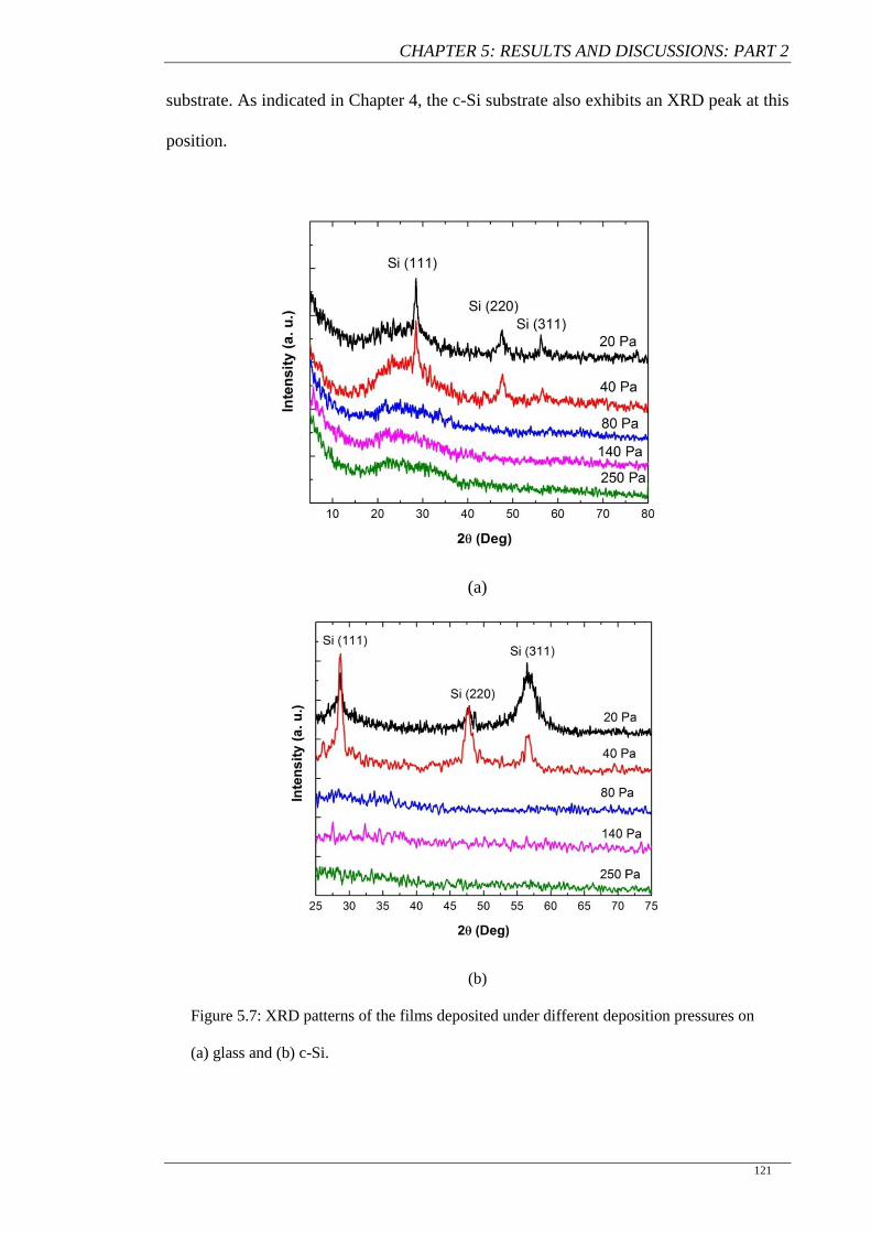
CHAPTER 5: RESULTS AND DISCUSSIONS: PART 2
121
substrate. As indicated in Chapter 4, the c-Si substrate also exhibits an XRD peak at this
position.
(a)
(b)
Figure 5.7: XRD patterns of the films deposited under different deposition pressures on
(a) glass and (b) c-Si.
CHAPTER 5: RESULTS AND DISCUSSIONS: PART 2
122
5.2.4 Elemental Composition
Figure 5.8 shows the average relative atomic concentration of silicon, carbon,
and oxygen in the films prepared at different deposition pressures. The atomic
concentration of carbon in the films prepared at 20 and 40 Pa was about 10%. However,
it was increased from ~10% to ~30% when the deposition pressure was increased from
40 to 80 Pa and remained almost constant with further increase in deposition pressure.
This indicates that the films deposited under deposition pressures below 80 Pa were Si-
rich as demonstrated by the FTIR spectra of these films. These films, however, showed
slightly higher oxygen content (~10-12 %), which was almost comparable to carbon
content. The oxygen concentration in the films however dropped with increasing
deposition pressure, which could be due to the significant increase in C incorporation
into the film structure.
Figure 5.8: The variation of relative atomic concentration of silicon, carbon and
oxygen in the films as a function of deposition pressure obtained from AES analysis.
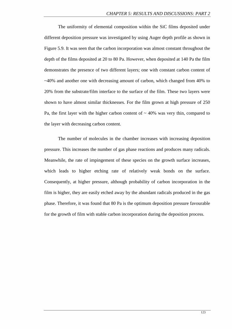
CHAPTER 5: RESULTS AND DISCUSSIONS: PART 2
123
The uniformity of elemental composition within the SiC films deposited under
different deposition pressure was investigated by using Auger depth profile as shown in
Figure 5.9. It was seen that the carbon incorporation was almost constant throughout the
depth of the films deposited at 20 to 80 Pa. However, when deposited at 140 Pa the film
demonstrates the presence of two different layers; one with constant carbon content of
~40% and another one with decreasing amount of carbon, which changed from 40% to
20% from the substrate/film interface to the surface of the film. These two layers were
shown to have almost similar thicknesses. For the film grown at high pressure of 250
Pa, the first layer with the higher carbon content of ~ 40% was very thin, compared to
the layer with decreasing carbon content.
The number of molecules in the chamber increases with increasing deposition
pressure. This increases the number of gas phase reactions and produces many radicals.
Meanwhile, the rate of impingement of these species on the growth surface increases,
which leads to higher etching rate of relatively weak bonds on the surface.
Consequently, at higher pressure, although probability of carbon incorporation in the
film is higher, they are easily etched away by the abundant radicals produced in the gas
phase. Therefore, it was found that 80 Pa is the optimum deposition pressure favourable
for the growth of film with stable carbon incorporation during the deposition process.
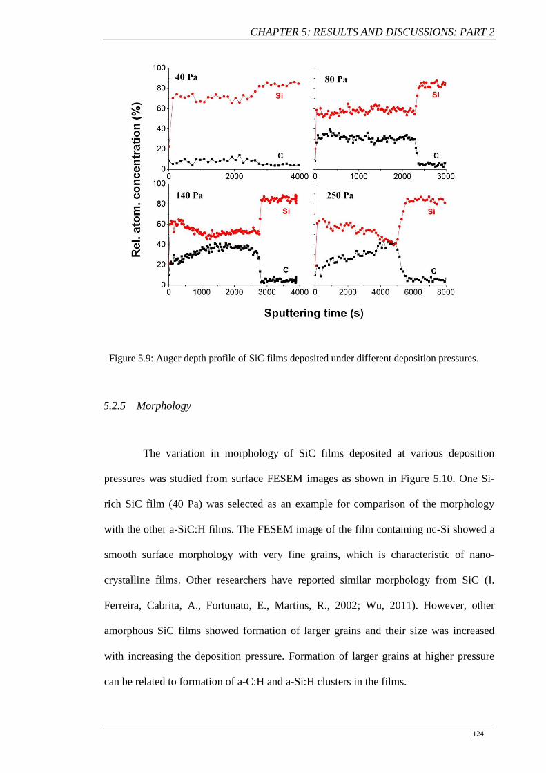
CHAPTER 5: RESULTS AND DISCUSSIONS: PART 2
124
Figure 5.9: Auger depth profile of SiC films deposited under different deposition pressures.
5.2.5 Morphology
The variation in morphology of SiC films deposited at various deposition
pressures was studied from surface FESEM images as shown in Figure 5.10. One Si-
rich SiC film (40 Pa) was selected as an example for comparison of the morphology
with the other a-SiC:H films. The FESEM image of the film containing nc-Si showed a
smooth surface morphology with very fine grains, which is characteristic of nano-
crystalline films. Other researchers have reported similar morphology from SiC (I.
Ferreira, Cabrita, A., Fortunato, E., Martins, R., 2002; Wu, 2011). However, other
amorphous SiC films showed formation of larger grains and their size was increased
with increasing the deposition pressure. Formation of larger grains at higher pressure
can be related to formation of a-C:H and a-Si:H clusters in the films.
CHAPTER 5: RESULTS AND DISCUSSIONS: PART 2
125
Low magnification High magnification
Figure 5.10: FESEM images of the surface of the films deposited at different
deposition pressures.
5 m 1 m
5 m 1 m
5 m
1 m 5 m
1 m
40 Pa
80 Pa
140 Pa
250 Pa
CHAPTER 5: RESULTS AND DISCUSSIONS: PART 2
126
5.2.6 Optical Properties
5.2.6.1 UV-Vis-NIR Spectroscopy
The optical properties of the SiC films deposited under different deposition
pressure were studied by UV-Vis-NIR transmission spectra as shown in Figure 5.11 (a).
It can be seen that the absorption edge was significantly blue-shifted with increasing
deposition pressure from 20 to 80 Pa. However, further increase in the deposition
pressure resulted in a red-shift in the absorption edge. The absorption coefficients of the
films deposited under different pressures were calculated using equation (3.16) and
shown in Figure 5.11 (b). The films prepared at low pressures below 80 Pa (Si-rich SiC
films) showed high absorption in the visible region, while the SiC films deposited at
higher pressure above 80 Pa were transparent in the wide range of the visible region. It
was noticed that there was a turning point for the film deposited at 80 Pa where the
transmission in the visible region was the highest.
The energy band gap of the films was calculated using Tauc’s plot (Tauc &
Abeles, 1972). Si-rich films prepared at 20 and 40 Pa had a band gap of 1.8 and 1.9 eV,
respectively. However, an increase in the deposition pressure from 40 to 80 Pa, has
remarkably increased the energy band gap up to 2.47 eV. This sharp increase in band
gap was shown to be parallel to the sudden increase in Si-C bonds in the film as shown
earlier (Figure 5. 2). The increase in the H content in the films deposited at higher
pressures may also contribute towards the increase in the energy gap in the films.
Further increase in the deposition pressure from 80 to 250 Pa, however, resulted in a
slight decrease in energy band gap of the film to 2.2 eV. This may be due to significant
increase in sp2-C bonds in the film structure.
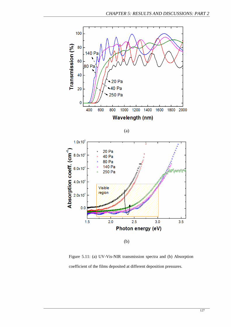
CHAPTER 5: RESULTS AND DISCUSSIONS: PART 2
127
(a)
(b)
Figure 5.11: (a) UV-Vis-NIR transmission spectra and (b) Absorption
coefficient of the films deposited at different deposition pressures.
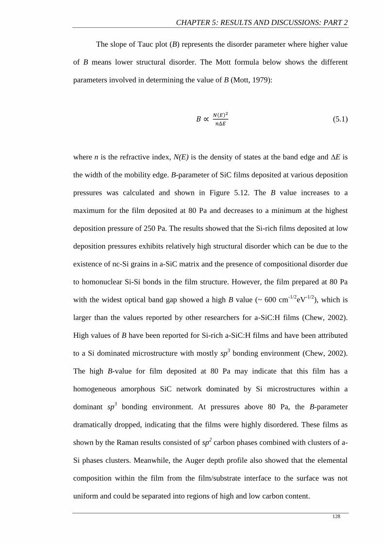
CHAPTER 5: RESULTS AND DISCUSSIONS: PART 2
128
The slope of Tauc plot (B) represents the disorder parameter where higher value
of B means lower structural disorder. The Mott formula below shows the different
parameters involved in determining the value of B (Mott, 1979):
( )
(5.1)
where n is the refractive index, N(E) is the density of states at the band edge and ∆E is
the width of the mobility edge. B-parameter of SiC films deposited at various deposition
pressures was calculated and shown in Figure 5.12. The B value increases to a
maximum for the film deposited at 80 Pa and decreases to a minimum at the highest
deposition pressure of 250 Pa. The results showed that the Si-rich films deposited at low
deposition pressures exhibits relatively high structural disorder which can be due to the
existence of nc-Si grains in a-SiC matrix and the presence of compositional disorder due
to homonuclear Si-Si bonds in the film structure. However, the film prepared at 80 Pa
with the widest optical band gap showed a high B value (~ 600 cm-1/2
eV-1/2
), which is
larger than the values reported by other researchers for a-SiC:H films (Chew, 2002).
High values of B have been reported for Si-rich a-SiC:H films and have been attributed
to a Si dominated microstructure with mostly sp3 bonding environment (Chew, 2002).
The high B-value for film deposited at 80 Pa may indicate that this film has a
homogeneous amorphous SiC network dominated by Si microstructures within a
dominant sp3 bonding environment. At pressures above 80 Pa, the B-parameter
dramatically dropped, indicating that the films were highly disordered. These films as
shown by the Raman results consisted of sp2 carbon phases combined with clusters of a-
Si phases clusters. Meanwhile, the Auger depth profile also showed that the elemental
composition within the film from the film/substrate interface to the surface was not
uniform and could be separated into regions of high and low carbon content.
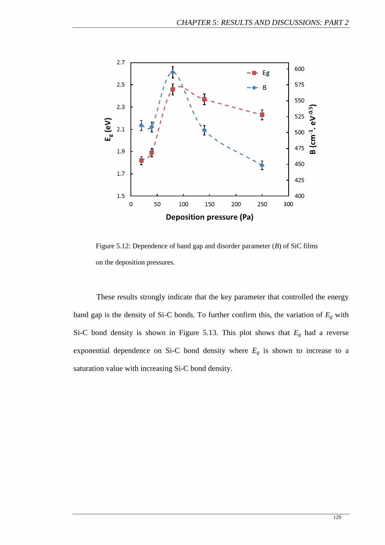
CHAPTER 5: RESULTS AND DISCUSSIONS: PART 2
129
Figure 5.12: Dependence of band gap and disorder parameter (B) of SiC films
on the deposition pressures.
These results strongly indicate that the key parameter that controlled the energy
band gap is the density of Si-C bonds. To further confirm this, the variation of Eg with
Si-C bond density is shown in Figure 5.13. This plot shows that Eg had a reverse
exponential dependence on Si-C bond density where Eg is shown to increase to a
saturation value with increasing Si-C bond density.
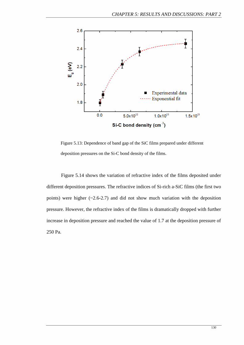
CHAPTER 5: RESULTS AND DISCUSSIONS: PART 2
130
Figure 5.13: Dependence of band gap of the SiC films prepared under different
deposition pressures on the Si-C bond density of the films.
Figure 5.14 shows the variation of refractive index of the films deposited under
different deposition pressures. The refractive indices of Si-rich a-SiC films (the first two
points) were higher (~2.6-2.7) and did not show much variation with the deposition
pressure. However, the refractive index of the films is dramatically dropped with further
increase in deposition pressure and reached the value of 1.7 at the deposition pressure of
250 Pa.
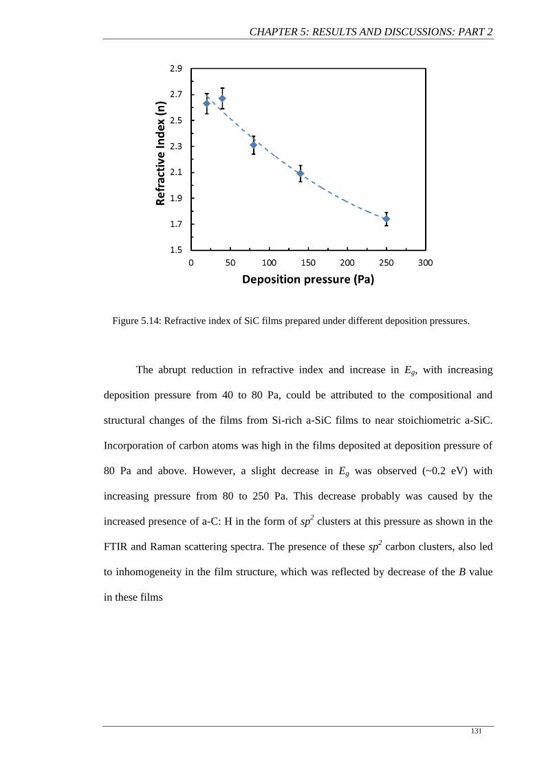
CHAPTER 5: RESULTS AND DISCUSSIONS: PART 2
131
Figure 5.14: Refractive index of SiC films prepared under different deposition pressures.
The abrupt reduction in refractive index and increase in Eg, with increasing
deposition pressure from 40 to 80 Pa, could be attributed to the compositional and
structural changes of the films from Si-rich a-SiC films to near stoichiometric a-SiC.
Incorporation of carbon atoms was high in the films deposited at deposition pressure of
80 Pa and above. However, a slight decrease in Eg was observed (~0.2 eV) with
increasing pressure from 80 to 250 Pa. This decrease probably was caused by the
increased presence of a-C: H in the form of sp2 clusters at this pressure as shown in the
FTIR and Raman scattering spectra. The presence of these sp2 carbon clusters, also led
to inhomogeneity in the film structure, which was reflected by decrease of the B value
in these films
CHAPTER 5: RESULTS AND DISCUSSIONS: PART 2
132
5.2.6.2 Photoluminescence Spectroscopy
Figure 5.15 shows room temperature photoluminescence (PL) spectra of SiC
films deposited under various deposition pressures. The films prepared at 20 and 40 Pa
exhibited a broad band centred at about 2.1 eV, which is greater than their optical band
gap. From structural and compositional characterizations, it was revealed that these
films are Si-rich with the presence of nc-Si grains in the amorphous matrix. It has been
reported that Si-rich a-SiC films did not produce PL emission at room temperature due
to quenching effect (Chew, 2002). Chew et al. have explained that at room temperature,
the rate of nonradiative recombination through paramagnetic Si dangling bond states in
Si-rich a-SiC films is 10 orders of magnitude higher than that of the band tail radiative
recombination. However, they observed PL emission from only C-rich a-SiC films at
room temperature. Similarly, in another study of PL properties of a-SiC films, it has
been shown that the films with carbon content below 0.55 did not exhibit any PL
emission at room temperature (Q. Cheng & et al., 2008). However, higher carbon
content resulted in intense PL emission. Nevertheless, broad band room temperature PL
has been reported recently from the a-SiC films embedded with nc-Si (G. Ambrosone,
Basa, Coscia, & Passacantando, 2012). Reduction in the size of Si nano-crystallites led
to enhancement of PL emission and a blue-shift of its position. Therefore, PL band
observed in this work for the Si-rich films can be attributed to the existence of nano-
crystalline Si phase in the material.
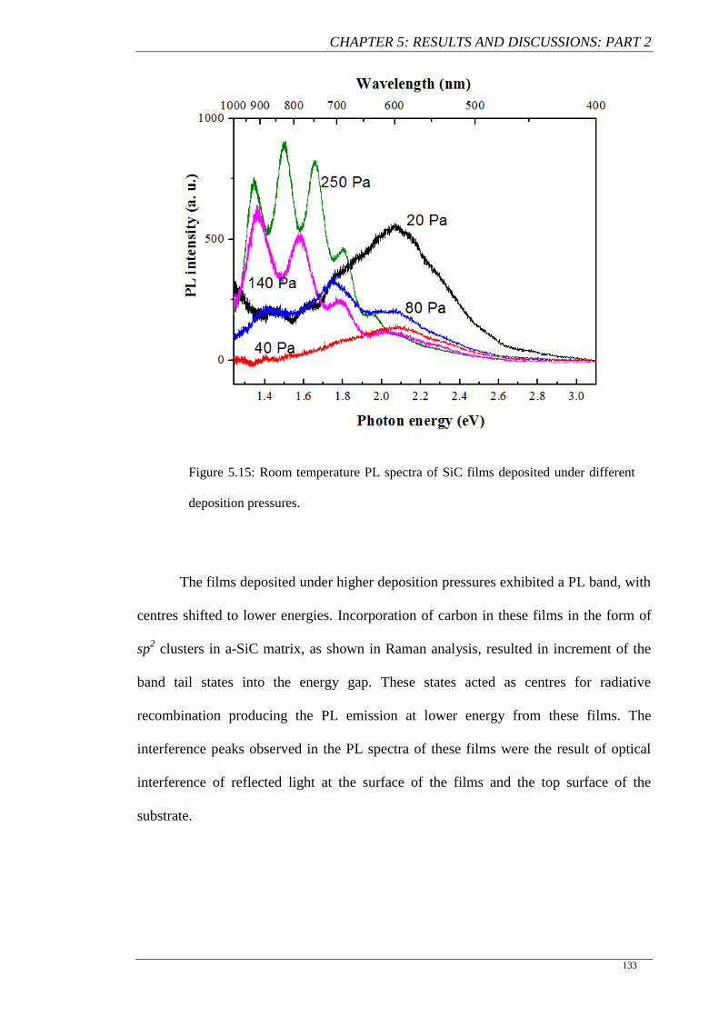
CHAPTER 5: RESULTS AND DISCUSSIONS: PART 2
133
Figure 5.15: Room temperature PL spectra of SiC films deposited under different
deposition pressures.
The films deposited under higher deposition pressures exhibited a PL band, with
centres shifted to lower energies. Incorporation of carbon in these films in the form of
sp2 clusters in a-SiC matrix, as shown in Raman analysis, resulted in increment of the
band tail states into the energy gap. These states acted as centres for radiative
recombination producing the PL emission at lower energy from these films. The
interference peaks observed in the PL spectra of these films were the result of optical
interference of reflected light at the surface of the films and the top surface of the
substrate.
CHAPTER 5: RESULTS AND DISCUSSIONS: PART 2
134
5.2.7 Deposition Rate
Figure 5.16 shows the deposition rate of the SiC films versus deposition
pressure. A sharp decrease in deposition rate from 0.7 to 0.45 nm/s was observed with
the increase in deposition pressure from 20 to 80 Pa. Further increase in pressure led to
a sharp increase in the deposition rate from 0.45 to 0.82 nm/s.
At low pressures (< 80 Pa), the probability of dissociating SiH4 molecules on the
hot-wire (HW) as Si and H atoms was high and the concentration of molecules in the
chamber was low. This allowed Si and H radicals to have a mean free path comparable
to the distance between HW and the substrate. Therefore, they were able to reach the
substrate surface directly or after only a few collisions with other molecules. As a result,
the number of gas phase reactions that usually lead to creation of C-related radicals was
limited and thus, Si-rich films were deposited under this condition. However,
bombardment of the growth surface by the H radicals promoted the crystallinity of Si
phase in the material as verified from XRD and Raman analysis. By increasing the
deposition pressure, the mean free path of Si molecules were reduced and they collided
with many more molecules or radicals before reaching the growth sites. This enabled
CH4 molecules to decompose through secondary gas phase reactions while decreasing
the deposition rate.
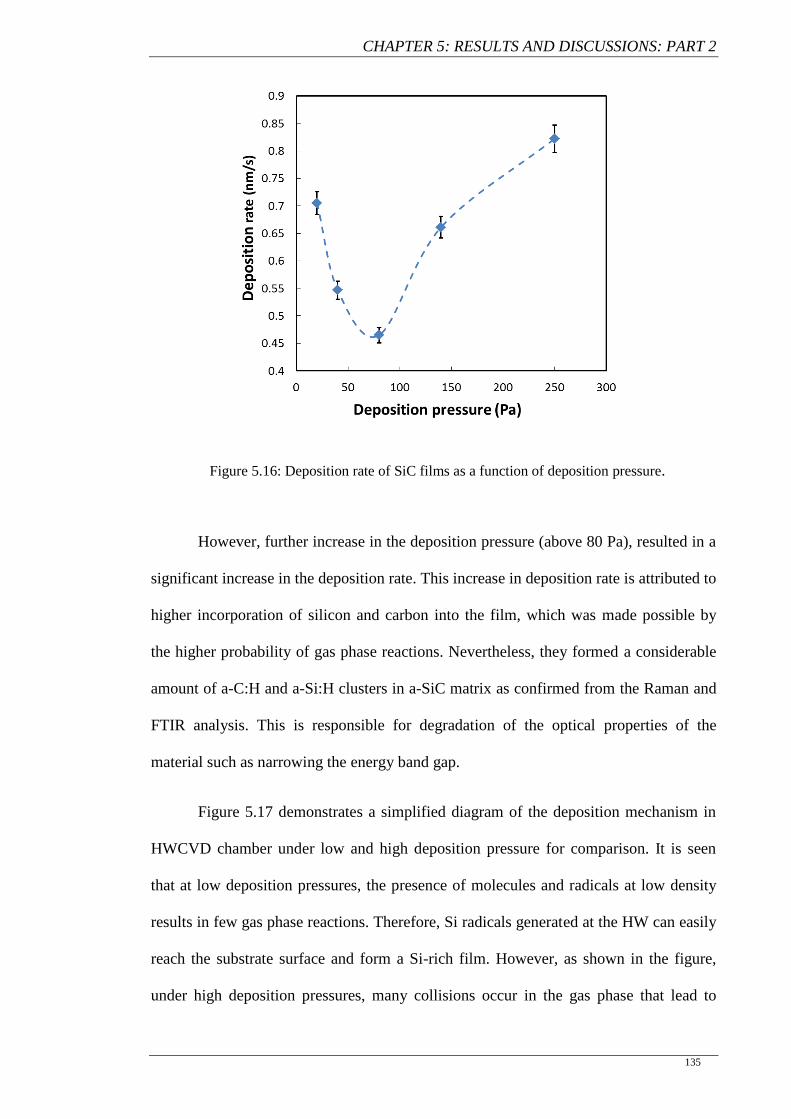
CHAPTER 5: RESULTS AND DISCUSSIONS: PART 2
135
Figure 5.16: Deposition rate of SiC films as a function of deposition pressure.
However, further increase in the deposition pressure (above 80 Pa), resulted in a
significant increase in the deposition rate. This increase in deposition rate is attributed to
higher incorporation of silicon and carbon into the film, which was made possible by
the higher probability of gas phase reactions. Nevertheless, they formed a considerable
amount of a-C:H and a-Si:H clusters in a-SiC matrix as confirmed from the Raman and
FTIR analysis. This is responsible for degradation of the optical properties of the
material such as narrowing the energy band gap.
Figure 5.17 demonstrates a simplified diagram of the deposition mechanism in
HWCVD chamber under low and high deposition pressure for comparison. It is seen
that at low deposition pressures, the presence of molecules and radicals at low density
results in few gas phase reactions. Therefore, Si radicals generated at the HW can easily
reach the substrate surface and form a Si-rich film. However, as shown in the figure,
under high deposition pressures, many collisions occur in the gas phase that lead to
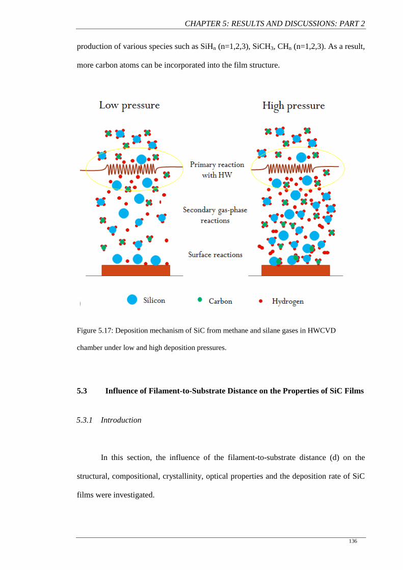
CHAPTER 5: RESULTS AND DISCUSSIONS: PART 2
136
production of various species such as SiHn (n=1,2,3), SiCH3, CHn (n=1,2,3). As a result,
more carbon atoms can be incorporated into the film structure.
Figure 5.17: Deposition mechanism of SiC from methane and silane gases in HWCVD
chamber under low and high deposition pressures.
5.3 Influence of Filament-to-Substrate Distance on the Properties of SiC Films
5.3.1 Introduction
In this section, the influence of the filament-to-substrate distance (d) on the
structural, compositional, crystallinity, optical properties and the deposition rate of SiC
films were investigated.
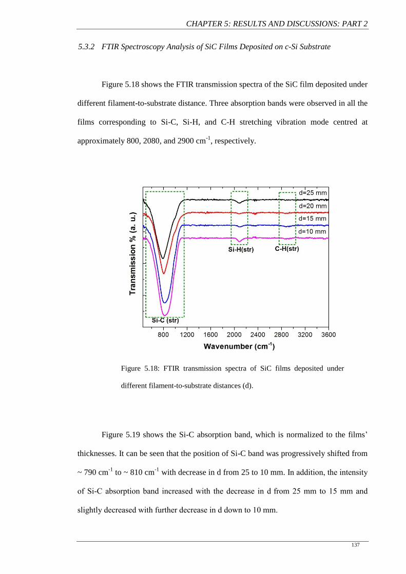
CHAPTER 5: RESULTS AND DISCUSSIONS: PART 2
137
5.3.2 FTIR Spectroscopy Analysis of SiC Films Deposited on c-Si Substrate
Figure 5.18 shows the FTIR transmission spectra of the SiC film deposited under
different filament-to-substrate distance. Three absorption bands were observed in all the
films corresponding to Si-C, Si-H, and C-H stretching vibration mode centred at
approximately 800, 2080, and 2900 cm-1
, respectively.
Figure 5.18: FTIR transmission spectra of SiC films deposited under
different filament-to-substrate distances (d).
Figure 5.19 shows the Si-C absorption band, which is normalized to the films’
thicknesses. It can be seen that the position of Si-C band was progressively shifted from
~ 790 cm-1
to ~ 810 cm-1
with decrease in d from 25 to 10 mm. In addition, the intensity
of Si-C absorption band increased with the decrease in d from 25 mm to 15 mm and
slightly decreased with further decrease in d down to 10 mm.
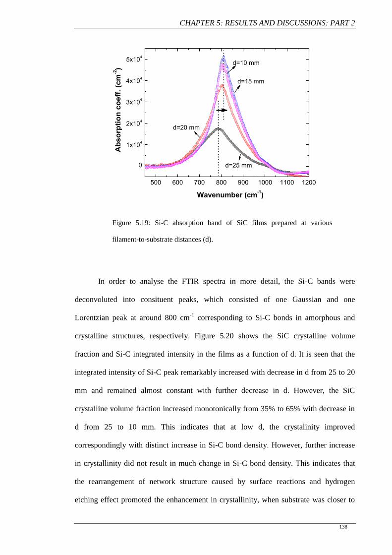
CHAPTER 5: RESULTS AND DISCUSSIONS: PART 2
138
Figure 5.19: Si-C absorption band of SiC films prepared at various
filament-to-substrate distances (d).
In order to analyse the FTIR spectra in more detail, the Si-C bands were
deconvoluted into consituent peaks, which consisted of one Gaussian and one
Lorentzian peak at around 800 cm-1
corresponding to Si-C bonds in amorphous and
crystalline structures, respectively. Figure 5.20 shows the SiC crystalline volume
fraction and Si-C integrated intensity in the films as a function of d. It is seen that the
integrated intensity of Si-C peak remarkably increased with decrease in d from 25 to 20
mm and remained almost constant with further decrease in d. However, the SiC
crystalline volume fraction increased monotonically from 35% to 65% with decrease in
d from 25 to 10 mm. This indicates that at low d, the crystalinity improved
correspondingly with distinct increase in Si-C bond density. However, further increase
in crystallinity did not result in much change in Si-C bond density. This indicates that
the rearrangement of network structure caused by surface reactions and hydrogen
etching effect promoted the enhancement in crystallinity, when substrate was closer to
500 600 700 800 900 1000 1100 1200
0
1x10⁴
2x10⁴
3x10⁴
4x10⁴
5x10⁴
d=15 mm
d=10 mm
d=25 mm
Ab
so
rpti
on
co
eff
. (c
m-2)
Wavenumber (cm-1)
d=20 mm
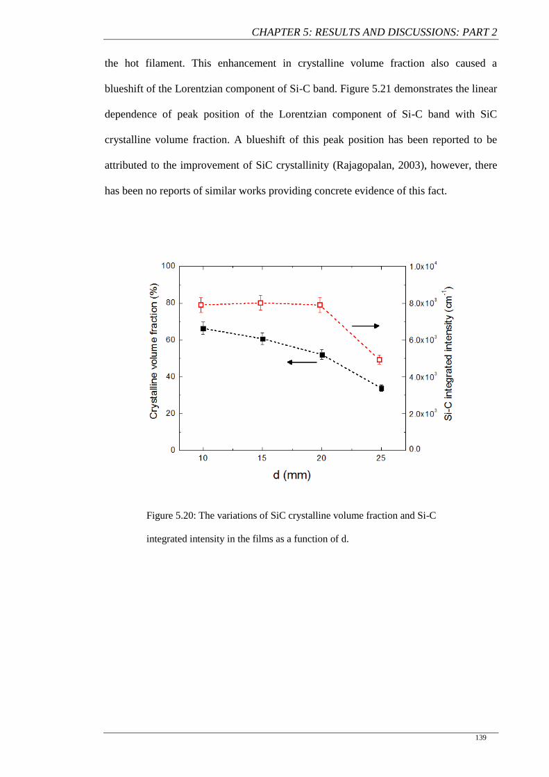
CHAPTER 5: RESULTS AND DISCUSSIONS: PART 2
139
the hot filament. This enhancement in crystalline volume fraction also caused a
blueshift of the Lorentzian component of Si-C band. Figure 5.21 demonstrates the linear
dependence of peak position of the Lorentzian component of Si-C band with SiC
crystalline volume fraction. A blueshift of this peak position has been reported to be
attributed to the improvement of SiC crystallinity (Rajagopalan, 2003), however, there
has been no reports of similar works providing concrete evidence of this fact.
Figure 5.20: The variations of SiC crystalline volume fraction and Si-C
integrated intensity in the films as a function of d.
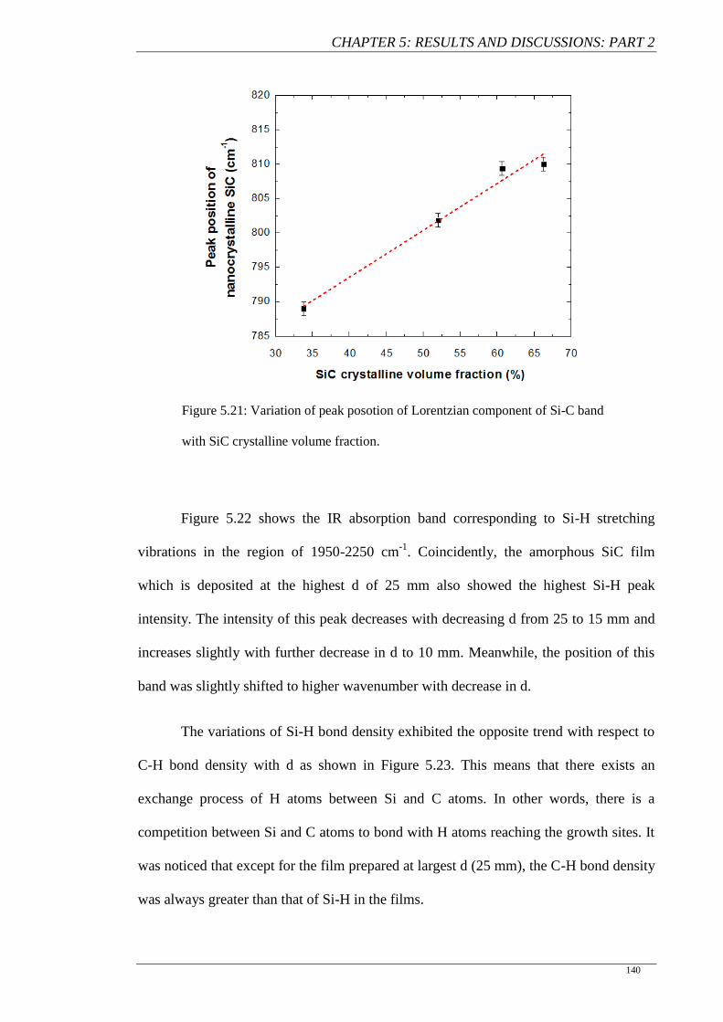
CHAPTER 5: RESULTS AND DISCUSSIONS: PART 2
140
Figure 5.21: Variation of peak posotion of Lorentzian component of Si-C band
with SiC crystalline volume fraction.
Figure 5.22 shows the IR absorption band corresponding to Si-H stretching
vibrations in the region of 1950-2250 cm-1
. Coincidently, the amorphous SiC film
which is deposited at the highest d of 25 mm also showed the highest Si-H peak
intensity. The intensity of this peak decreases with decreasing d from 25 to 15 mm and
increases slightly with further decrease in d to 10 mm. Meanwhile, the position of this
band was slightly shifted to higher wavenumber with decrease in d.
The variations of Si-H bond density exhibited the opposite trend with respect to
C-H bond density with d as shown in Figure 5.23. This means that there exists an
exchange process of H atoms between Si and C atoms. In other words, there is a
competition between Si and C atoms to bond with H atoms reaching the growth sites. It
was noticed that except for the film prepared at largest d (25 mm), the C-H bond density
was always greater than that of Si-H in the films.
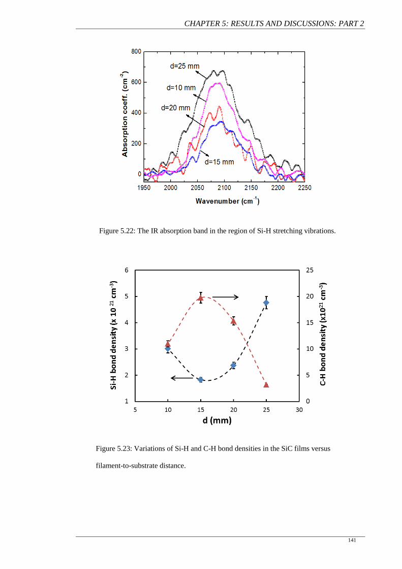
CHAPTER 5: RESULTS AND DISCUSSIONS: PART 2
141
Figure 5.22: The IR absorption band in the region of Si-H stretching vibrations.
Figure 5.23: Variations of Si-H and C-H bond densities in the SiC films versus
filament-to-substrate distance.
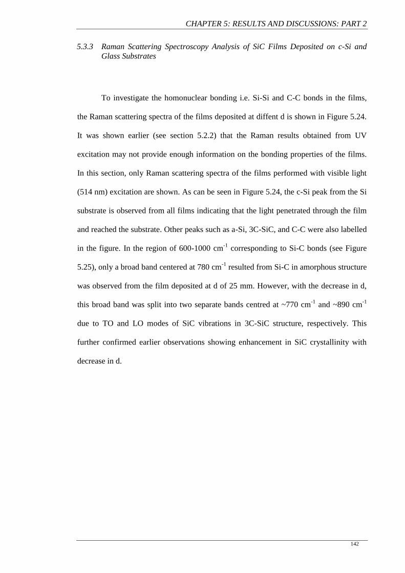
CHAPTER 5: RESULTS AND DISCUSSIONS: PART 2
142
5.3.3 Raman Scattering Spectroscopy Analysis of SiC Films Deposited on c-Si and
Glass Substrates
To investigate the homonuclear bonding i.e. Si-Si and C-C bonds in the films,
the Raman scattering spectra of the films deposited at diffent d is shown in Figure 5.24.
It was shown earlier (see section 5.2.2) that the Raman results obtained from UV
excitation may not provide enough information on the bonding properties of the films.
In this section, only Raman scattering spectra of the films performed with visible light
(514 nm) excitation are shown. As can be seen in Figure 5.24, the c-Si peak from the Si
substrate is observed from all films indicating that the light penetrated through the film
and reached the substrate. Other peaks such as a-Si, 3C-SiC, and C-C were also labelled
in the figure. In the region of 600-1000 cm-1
corresponding to Si-C bonds (see Figure
5.25), only a broad band centered at 780 cm-1
resulted from Si-C in amorphous structure
was observed from the film deposited at d of 25 mm. However, with the decrease in d,
this broad band was split into two separate bands centred at ~770 cm-1
and ~890 cm-1
due to TO and LO modes of SiC vibrations in 3C-SiC structure, respectively. This
further confirmed earlier observations showing enhancement in SiC crystallinity with
decrease in d.
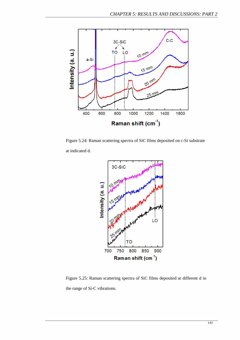
CHAPTER 5: RESULTS AND DISCUSSIONS: PART 2
143
Figure 5.24: Raman scattering spectra of SiC films deposited on c-Si substrate
at indicated d.
Figure 5.25: Raman scattering spectra of SiC films deposited at different d in
the range of Si-C vibrations.
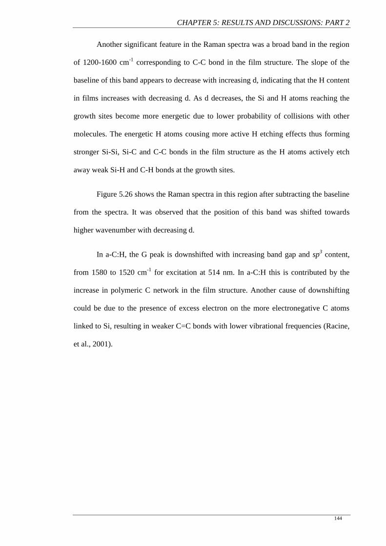
CHAPTER 5: RESULTS AND DISCUSSIONS: PART 2
144
Another significant feature in the Raman spectra was a broad band in the region
of 1200-1600 cm-1
corresponding to C-C bond in the film structure. The slope of the
baseline of this band appears to decrease with increasing d, indicating that the H content
in films increases with decreasing d. As d decreases, the Si and H atoms reaching the
growth sites become more energetic due to lower probability of collisions with other
molecules. The energetic H atoms cousing more active H etching effects thus forming
stronger Si-Si, Si-C and C-C bonds in the film structure as the H atoms actively etch
away weak Si-H and C-H bonds at the growth sites.
Figure 5.26 shows the Raman spectra in this region after subtracting the baseline
from the spectra. It was observed that the position of this band was shifted towards
higher wavenumber with decreasing d.
In a-C:H, the G peak is downshifted with increasing band gap and sp3 content,
from 1580 to 1520 cm-1
for excitation at 514 nm. In a-C:H this is contributed by the
increase in polymeric C network in the film structure. Another cause of downshifting
could be due to the presence of excess electron on the more electronegative C atoms
linked to Si, resulting in weaker C=C bonds with lower vibrational frequencies (Racine,
et al., 2001).
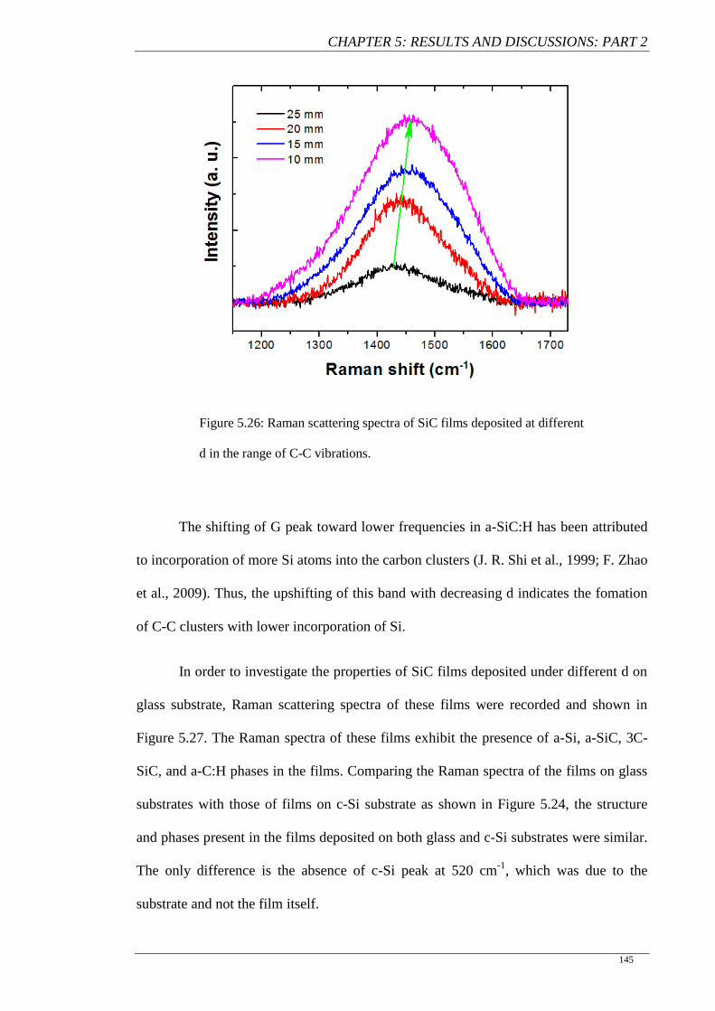
CHAPTER 5: RESULTS AND DISCUSSIONS: PART 2
145
Figure 5.26: Raman scattering spectra of SiC films deposited at different
d in the range of C-C vibrations.
The shifting of G peak toward lower frequencies in a-SiC:H has been attributed
to incorporation of more Si atoms into the carbon clusters (J. R. Shi et al., 1999; F. Zhao
et al., 2009). Thus, the upshifting of this band with decreasing d indicates the fomation
of C-C clusters with lower incorporation of Si.
In order to investigate the properties of SiC films deposited under different d on
glass substrate, Raman scattering spectra of these films were recorded and shown in
Figure 5.27. The Raman spectra of these films exhibit the presence of a-Si, a-SiC, 3C-
SiC, and a-C:H phases in the films. Comparing the Raman spectra of the films on glass
substrates with those of films on c-Si substrate as shown in Figure 5.24, the structure
and phases present in the films deposited on both glass and c-Si substrates were similar.
The only difference is the absence of c-Si peak at 520 cm-1
, which was due to the
substrate and not the film itself.
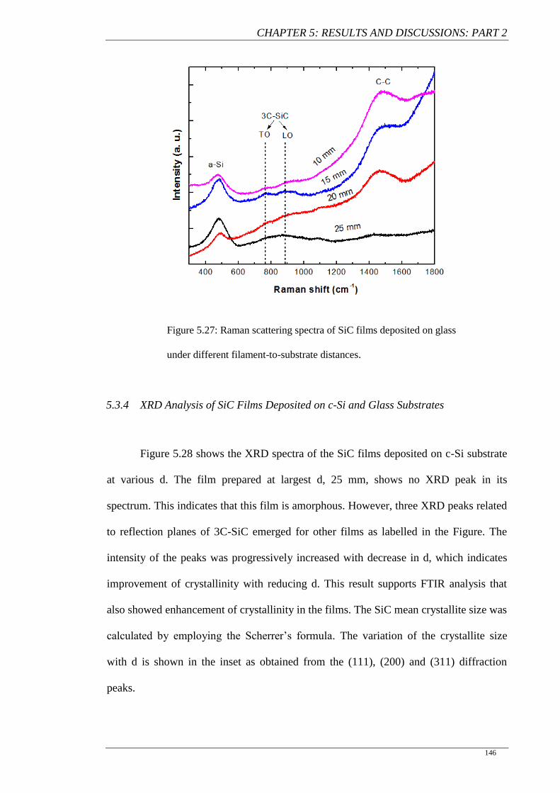
CHAPTER 5: RESULTS AND DISCUSSIONS: PART 2
146
Figure 5.27: Raman scattering spectra of SiC films deposited on glass
under different filament-to-substrate distances.
5.3.4 XRD Analysis of SiC Films Deposited on c-Si and Glass Substrates
Figure 5.28 shows the XRD spectra of the SiC films deposited on c-Si substrate
at various d. The film prepared at largest d, 25 mm, shows no XRD peak in its
spectrum. This indicates that this film is amorphous. However, three XRD peaks related
to reflection planes of 3C-SiC emerged for other films as labelled in the Figure. The
intensity of the peaks was progressively increased with decrease in d, which indicates
improvement of crystallinity with reducing d. This result supports FTIR analysis that
also showed enhancement of crystallinity in the films. The SiC mean crystallite size was
calculated by employing the Scherrer’s formula. The variation of the crystallite size
with d is shown in the inset as obtained from the (111), (200) and (311) diffraction
peaks.
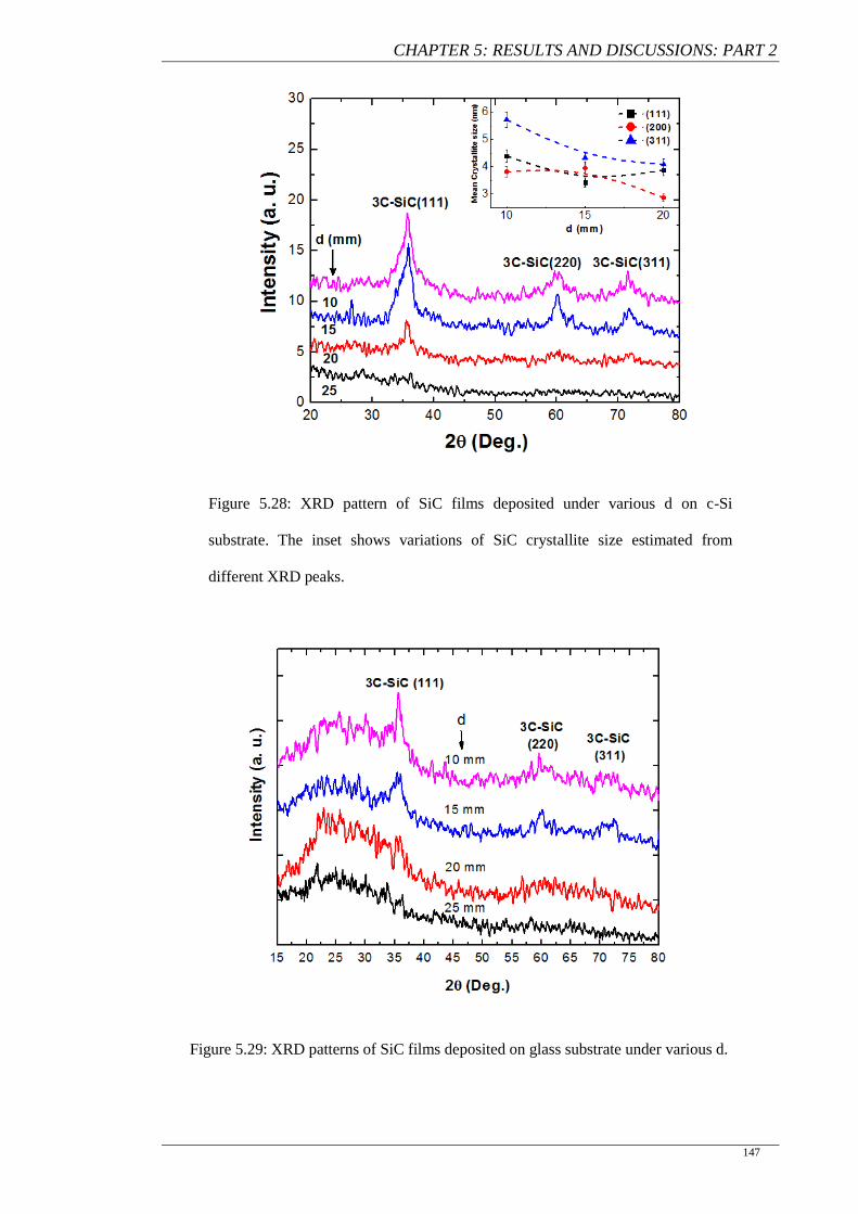
CHAPTER 5: RESULTS AND DISCUSSIONS: PART 2
147
Figure 5.28: XRD pattern of SiC films deposited under various d on c-Si
substrate. The inset shows variations of SiC crystallite size estimated from
different XRD peaks.
Figure 5.29: XRD patterns of SiC films deposited on glass substrate under various d.
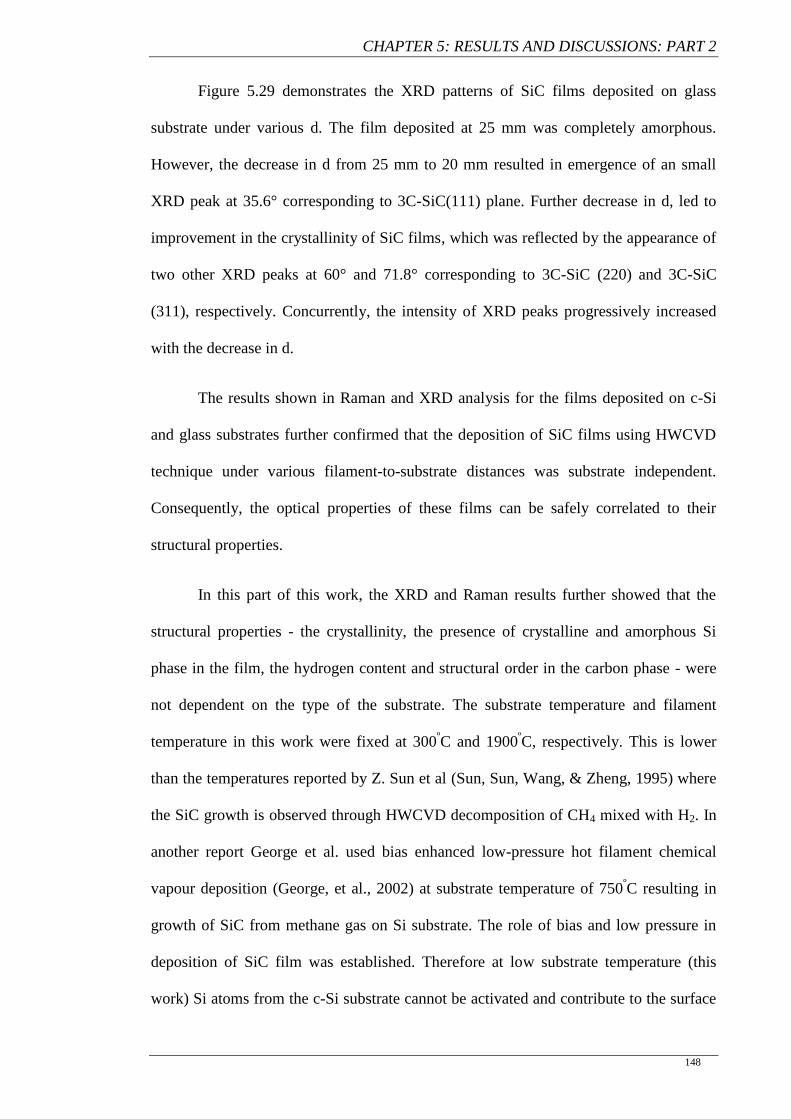
CHAPTER 5: RESULTS AND DISCUSSIONS: PART 2
148
Figure 5.29 demonstrates the XRD patterns of SiC films deposited on glass
substrate under various d. The film deposited at 25 mm was completely amorphous.
However, the decrease in d from 25 mm to 20 mm resulted in emergence of an small
XRD peak at 35.6° corresponding to 3C-SiC(111) plane. Further decrease in d, led to
improvement in the crystallinity of SiC films, which was reflected by the appearance of
two other XRD peaks at 60° and 71.8° corresponding to 3C-SiC (220) and 3C-SiC
(311), respectively. Concurrently, the intensity of XRD peaks progressively increased
with the decrease in d.
The results shown in Raman and XRD analysis for the films deposited on c-Si
and glass substrates further confirmed that the deposition of SiC films using HWCVD
technique under various filament-to-substrate distances was substrate independent.
Consequently, the optical properties of these films can be safely correlated to their
structural properties.
In this part of this work, the XRD and Raman results further showed that the
structural properties - the crystallinity, the presence of crystalline and amorphous Si
phase in the film, the hydrogen content and structural order in the carbon phase - were
not dependent on the type of the substrate. The substrate temperature and filament
temperature in this work were fixed at 300ºC and 1900
ºC, respectively. This is lower
than the temperatures reported by Z. Sun et al (Sun, Sun, Wang, & Zheng, 1995) where
the SiC growth is observed through HWCVD decomposition of CH4 mixed with H2. In
another report George et al. used bias enhanced low-pressure hot filament chemical
vapour deposition (George, et al., 2002) at substrate temperature of 750ºC resulting in
growth of SiC from methane gas on Si substrate. The role of bias and low pressure in
deposition of SiC film was established. Therefore at low substrate temperature (this
work) Si atoms from the c-Si substrate cannot be activated and contribute to the surface
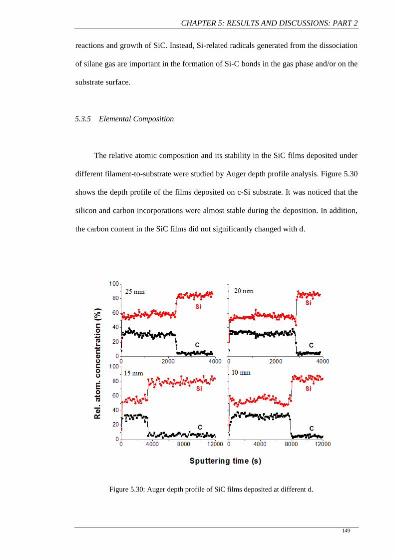
CHAPTER 5: RESULTS AND DISCUSSIONS: PART 2
149
reactions and growth of SiC. Instead, Si-related radicals generated from the dissociation
of silane gas are important in the formation of Si-C bonds in the gas phase and/or on the
substrate surface.
5.3.5 Elemental Composition
The relative atomic composition and its stability in the SiC films deposited under
different filament-to-substrate were studied by Auger depth profile analysis. Figure 5.30
shows the depth profile of the films deposited on c-Si substrate. It was noticed that the
silicon and carbon incorporations were almost stable during the deposition. In addition,
the carbon content in the SiC films did not significantly changed with d.
Figure 5.30: Auger depth profile of SiC films deposited at different d.
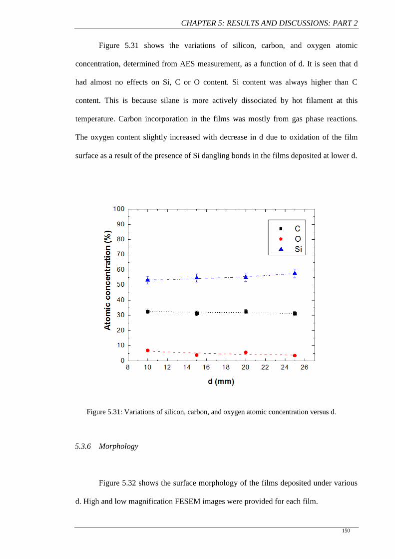
CHAPTER 5: RESULTS AND DISCUSSIONS: PART 2
150
Figure 5.31 shows the variations of silicon, carbon, and oxygen atomic
concentration, determined from AES measurement, as a function of d. It is seen that d
had almost no effects on Si, C or O content. Si content was always higher than C
content. This is because silane is more actively dissociated by hot filament at this
temperature. Carbon incorporation in the films was mostly from gas phase reactions.
The oxygen content slightly increased with decrease in d due to oxidation of the film
surface as a result of the presence of Si dangling bonds in the films deposited at lower d.
Figure 5.31: Variations of silicon, carbon, and oxygen atomic concentration versus d.
5.3.6 Morphology
Figure 5.32 shows the surface morphology of the films deposited under various
d. High and low magnification FESEM images were provided for each film.
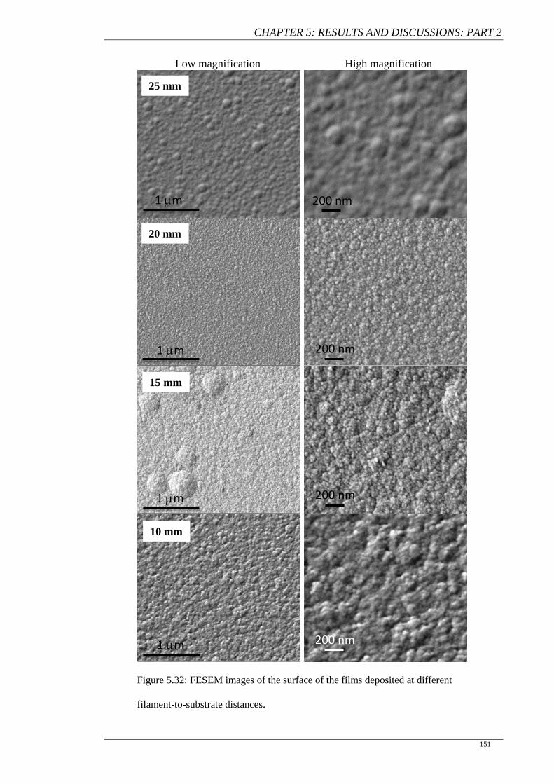
CHAPTER 5: RESULTS AND DISCUSSIONS: PART 2
151
Low magnification High magnification
Figure 5.32: FESEM images of the surface of the films deposited at different
filament-to-substrate distances.
1 m 200 nm
1 m
1 m
1 m
200 nm
200 nm
200 nm
10 mm
15 mm
20 mm
25 mm
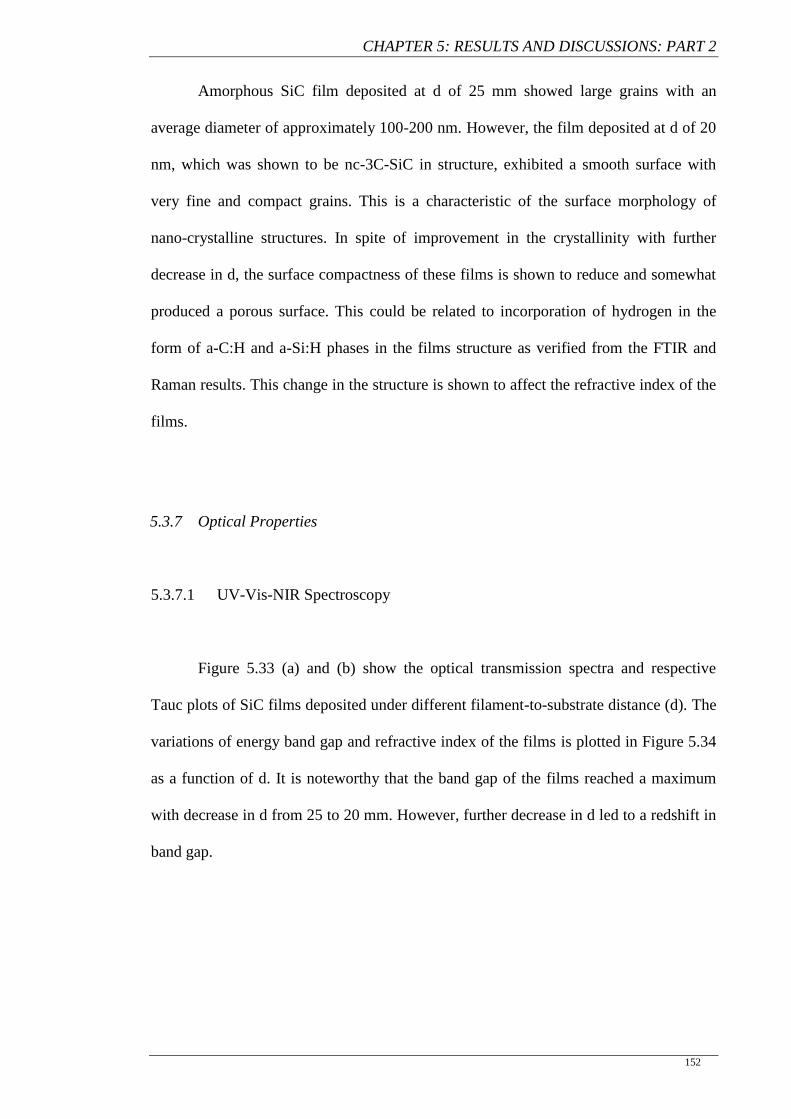
CHAPTER 5: RESULTS AND DISCUSSIONS: PART 2
152
Amorphous SiC film deposited at d of 25 mm showed large grains with an
average diameter of approximately 100-200 nm. However, the film deposited at d of 20
nm, which was shown to be nc-3C-SiC in structure, exhibited a smooth surface with
very fine and compact grains. This is a characteristic of the surface morphology of
nano-crystalline structures. In spite of improvement in the crystallinity with further
decrease in d, the surface compactness of these films is shown to reduce and somewhat
produced a porous surface. This could be related to incorporation of hydrogen in the
form of a-C:H and a-Si:H phases in the films structure as verified from the FTIR and
Raman results. This change in the structure is shown to affect the refractive index of the
films.
5.3.7 Optical Properties
5.3.7.1 UV-Vis-NIR Spectroscopy
Figure 5.33 (a) and (b) show the optical transmission spectra and respective
Tauc plots of SiC films deposited under different filament-to-substrate distance (d). The
variations of energy band gap and refractive index of the films is plotted in Figure 5.34
as a function of d. It is noteworthy that the band gap of the films reached a maximum
with decrease in d from 25 to 20 mm. However, further decrease in d led to a redshift in
band gap.
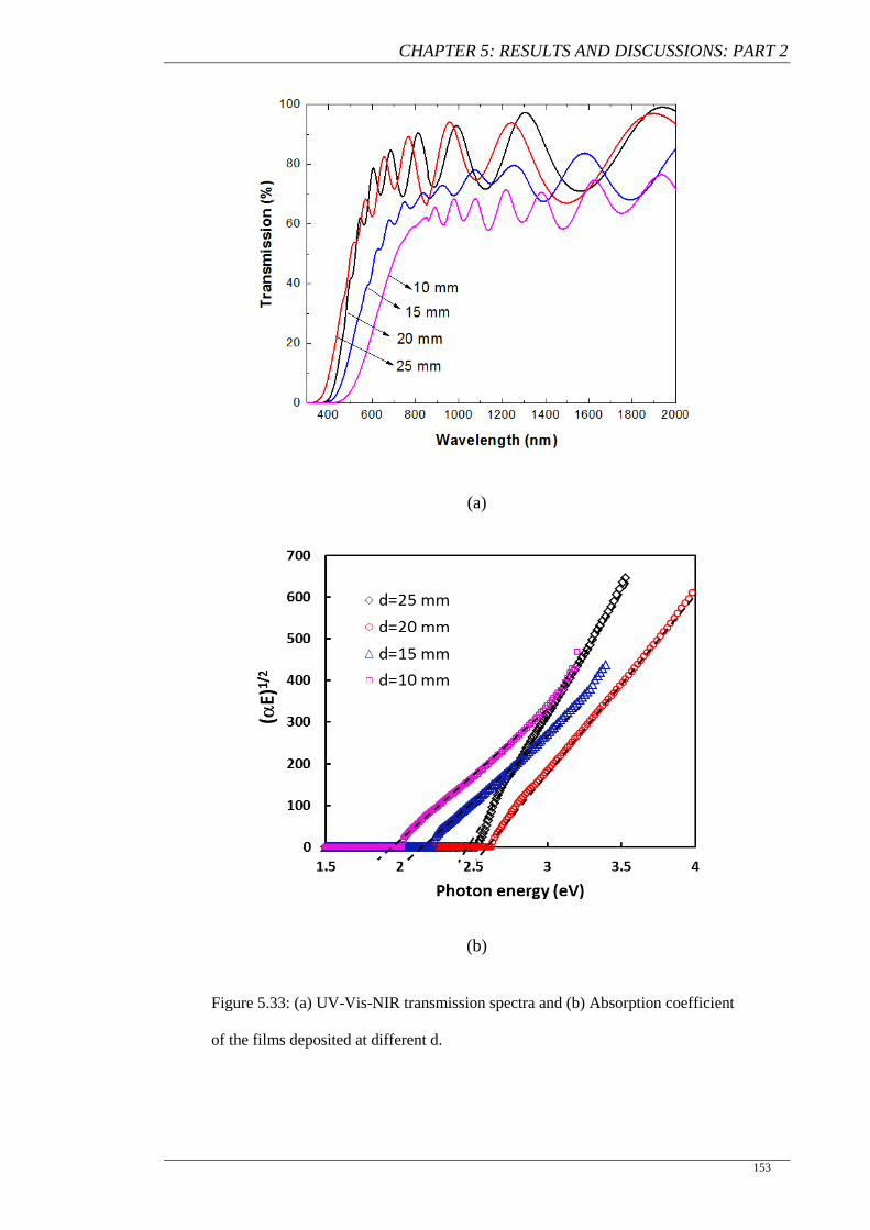
CHAPTER 5: RESULTS AND DISCUSSIONS: PART 2
153
(a)
(b)
Figure 5.33: (a) UV-Vis-NIR transmission spectra and (b) Absorption coefficient
of the films deposited at different d.
CHAPTER 5: RESULTS AND DISCUSSIONS: PART 2
154
Figure 5.34: Band gap and refractive index of SiC films deposited under different d.
The widening of band gap with the decrease in d originated from significant
enhancement of Si-C bond density along with the formation of 3C-SiC nano-crystallite
in the film as shown in FTIR and XRD results. Nevertheless, the decrease in energy
band gap with further decrease in d did not show any direct dependence on Si-C bond
density. The total Si-C bond density in the films did not significantly change with
decrease in d from 20 to 10 mm, but the crystallinity of SiC network improved, which
was reflected by the enhancement of SiC crystalline volume fraction (see Figure 5.20).
Therefore, the narrowing of the energy band gap can be explained by the agglomeration
of sp2 carbon that was observed through Raman spectra. It was found that the C-C band
in Raman spectra of these films broadened and shifted to the higher wavenumbers along
with the decrease in the energy band gap, which indicates formation of pure a-C:H
clusters in the films (M. Park et al., 2001).
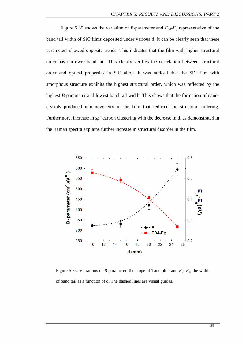
CHAPTER 5: RESULTS AND DISCUSSIONS: PART 2
155
Figure 5.35 shows the variation of B-parameter and E04-Eg representative of the
band tail width of SiC films deposited under various d. It can be clearly seen that these
parameters showed opposite trends. This indicates that the film with higher structural
order has narrower band tail. This clearly verifies the correlation between structural
order and optical properties in SiC alloy. It was noticed that the SiC film with
amorphous structure exhibits the highest structural order, which was reflected by the
highest B-parameter and lowest band tail width. This shows that the formation of nano-
crystals produced inhomogeneity in the film that reduced the structural ordering.
Furthermore, increase in sp2 carbon clustering with the decrease in d, as demonstrated in
the Raman spectra explains further increase in structural disorder in the film.
Figure 5.35: Variations of B-parameter, the slope of Tauc plot, and E04-Eg, the width
of band tail as a function of d. The dashed lines are visual guides.
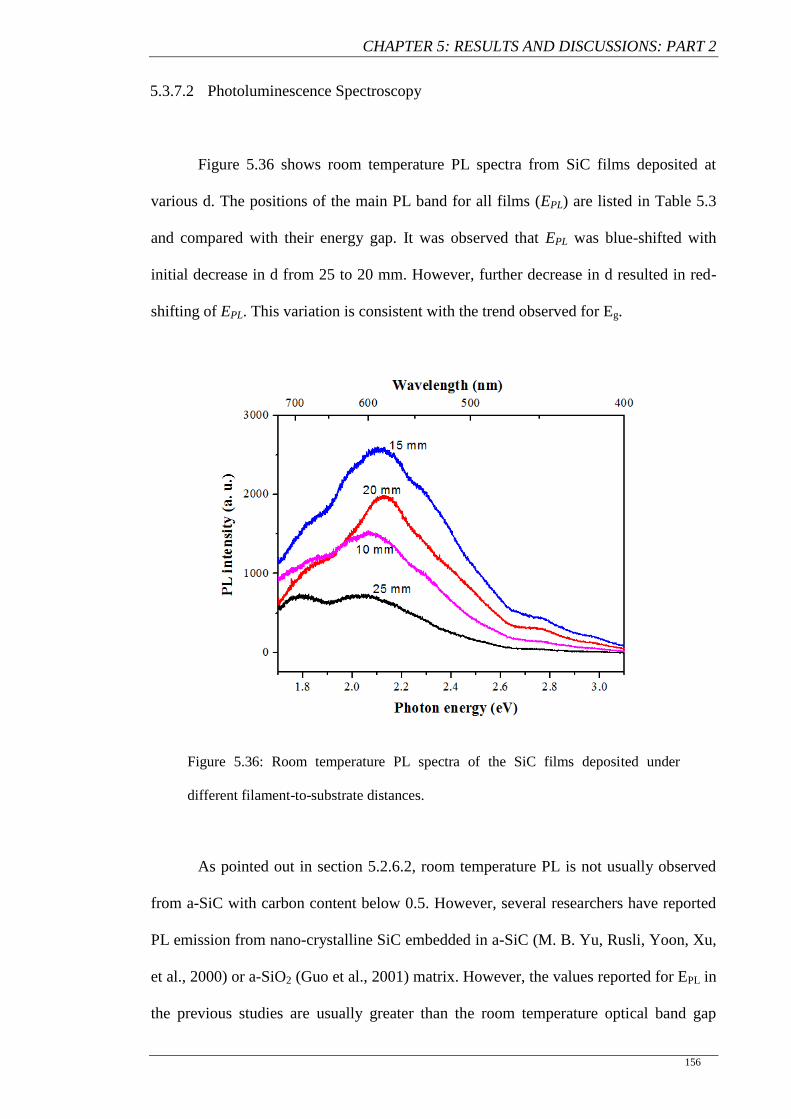
CHAPTER 5: RESULTS AND DISCUSSIONS: PART 2
156
5.3.7.2 Photoluminescence Spectroscopy
Figure 5.36 shows room temperature PL spectra from SiC films deposited at
various d. The positions of the main PL band for all films (EPL) are listed in Table 5.3
and compared with their energy gap. It was observed that EPL was blue-shifted with
initial decrease in d from 25 to 20 mm. However, further decrease in d resulted in red-
shifting of EPL. This variation is consistent with the trend observed for Eg.
Figure 5.36: Room temperature PL spectra of the SiC films deposited under
different filament-to-substrate distances.
As pointed out in section 5.2.6.2, room temperature PL is not usually observed
from a-SiC with carbon content below 0.5. However, several researchers have reported
PL emission from nano-crystalline SiC embedded in a-SiC (M. B. Yu, Rusli, Yoon, Xu,
et al., 2000) or a-SiO2 (Guo et al., 2001) matrix. However, the values reported for EPL in
the previous studies are usually greater than the room temperature optical band gap
CHAPTER 5: RESULTS AND DISCUSSIONS: PART 2
157
energy of the bulk 3C-SiC. For example, Yu et al. have reported a PL energy of 2.6 eV
attributed to the quantum size effect in SiC nano-crystallites (M. B. Yu, Rusli, Yoon,
Xu, et al., 2000). In another study, visible PL emission with the energy of ~2.5 eV has
been observed from SiC nano-crystalline films, which is higher than the their energy
band gap (Xu, et al., 2000). Xu et al. have suggested that the origin of this intense
photon emission in the SiC nano-crystals is the radiative recombination due to the direct
optical transitions. Recently, Yu et al. have observed a PL emission showing a dominant
PL band centred at ~2.5 eV originated from radiative recombination in quantized states
of SiC nano-crystals and a weaker component at ~ 1.9 eV originated from radiative
recombination in the band tail states of amorphous SiC matrix (W. Yu et al., 2011).
Therefore, the PL spectra obtained in this work probably were not contributed by the
SiC nano-crystals. The radiative recombination resulted from band-to-band transition
and this process contributes to the dominant process for the PL emission. However,
radiative recombination in the band tail states of amorphous environment is responsible
for the peak shoulder detected in the lower energy region.
Table 5.3. PL energy and energy band gap of SiC films
deposited under different d.
d (mm)
EPL
(eV)
𝑉
Eg(eV)
𝑉
25 2.04 2.46
20 2.14 2.57
15 2.10 2.17
10 2.06 1.97
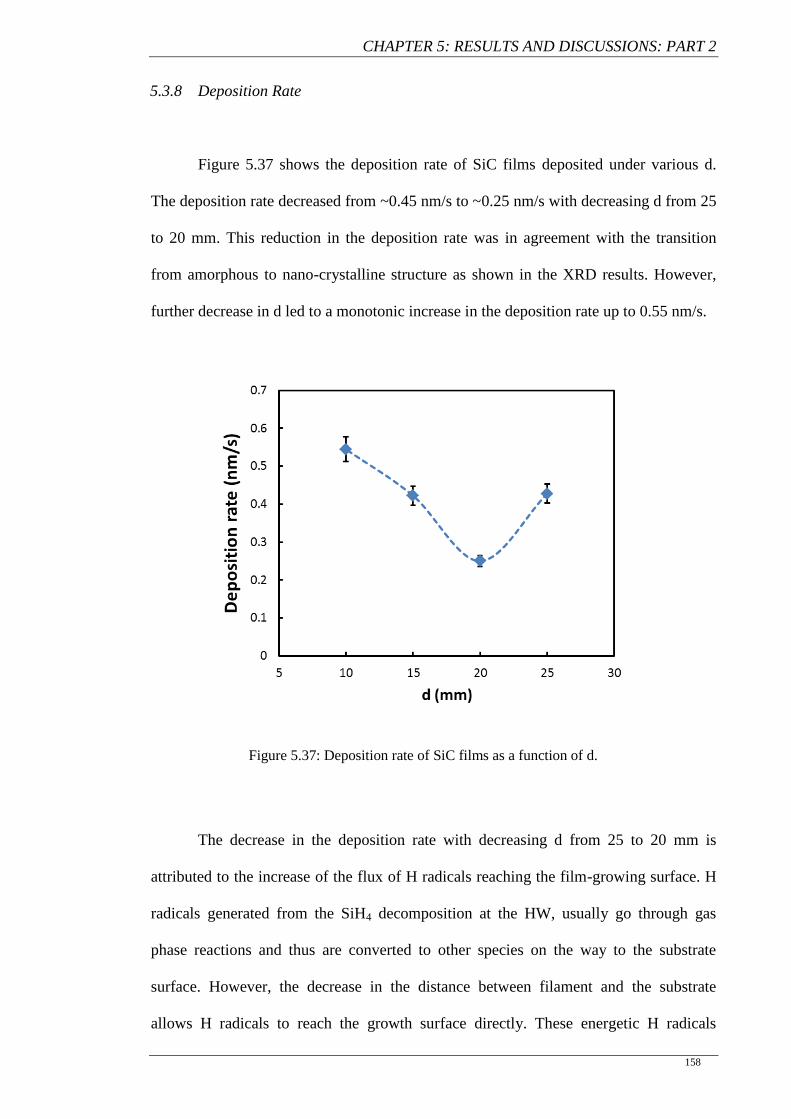
CHAPTER 5: RESULTS AND DISCUSSIONS: PART 2
158
5.3.8 Deposition Rate
Figure 5.37 shows the deposition rate of SiC films deposited under various d.
The deposition rate decreased from ~0.45 nm/s to ~0.25 nm/s with decreasing d from 25
to 20 mm. This reduction in the deposition rate was in agreement with the transition
from amorphous to nano-crystalline structure as shown in the XRD results. However,
further decrease in d led to a monotonic increase in the deposition rate up to 0.55 nm/s.
Figure 5.37: Deposition rate of SiC films as a function of d.
The decrease in the deposition rate with decreasing d from 25 to 20 mm is
attributed to the increase of the flux of H radicals reaching the film-growing surface. H
radicals generated from the SiH4 decomposition at the HW, usually go through gas
phase reactions and thus are converted to other species on the way to the substrate
surface. However, the decrease in the distance between filament and the substrate
allows H radicals to reach the growth surface directly. These energetic H radicals
CHAPTER 5: RESULTS AND DISCUSSIONS: PART 2
159
promote crystallinity in the film by penetrating the layers below the top surface of the
film and was caused the breaking of weak Si-H bonds, thus leading to formation of
ordered Si-C network. However, further improvement in crystallinity with decreasing d
led to an increase in the deposition rate. Similar enhancement of crystallinity and
deposition rate with reduction of d has been reported for nc-Si:H films deposited from
pure SiH4 gas by HWCVD technique (Waman, 2011). They attributed this increase in
deposition rate to the enhancement in the diffusion of radicals such as Si-H, Si-H2, or
(Si-H2)n. Nevertheless, in this work, the formation of C-Hn and sp2 C-C bonds seems to
contribute to enhancement of the deposition rate at lower d as shown in IR and Raman
results.
Figure 5.38 shows a simple illustration of the deposition mechanism in HWCVD
chamber under three different filament-to-substrate distances for comparison. It should
be noted that not all radicals species created in the gas phase are shown in the figure.
From what has been reported in the literature, in spite of extensive work done in radical
measurements from various techniques for Si deposition by HWCVD from SiH4/H2
gases (Nakamura & Koshi, 2006; Umemoto, 2002; Zheng & Gallagher, 2006), no direct
measurement or theoretical work on chemical reactions and radicals produced in the
HWCVD system with SiH4 and CH4 gases is available yet. Therefore, the detail of
chemical reactions and resulting radicals in the chamber is still unknown. However,
from this study, the role of H radicals in the crystallinity of the films was verified in
spite of absence of hydrogen dilution of the source gases. These abundant H radicals
were generated from the silane decomposition on the hot filament. When the filament is
placed far from the substrate, generated radicals on the HW including H radicals are
consumed through gas phase reactions. Therefore, the flux of H radicals reaching the
substrate surface is fairly low. Under this situation, formation of a significant amount of
SiHn, SiCHn, and CHn precursors led to deposition of amorphous SiC films with high
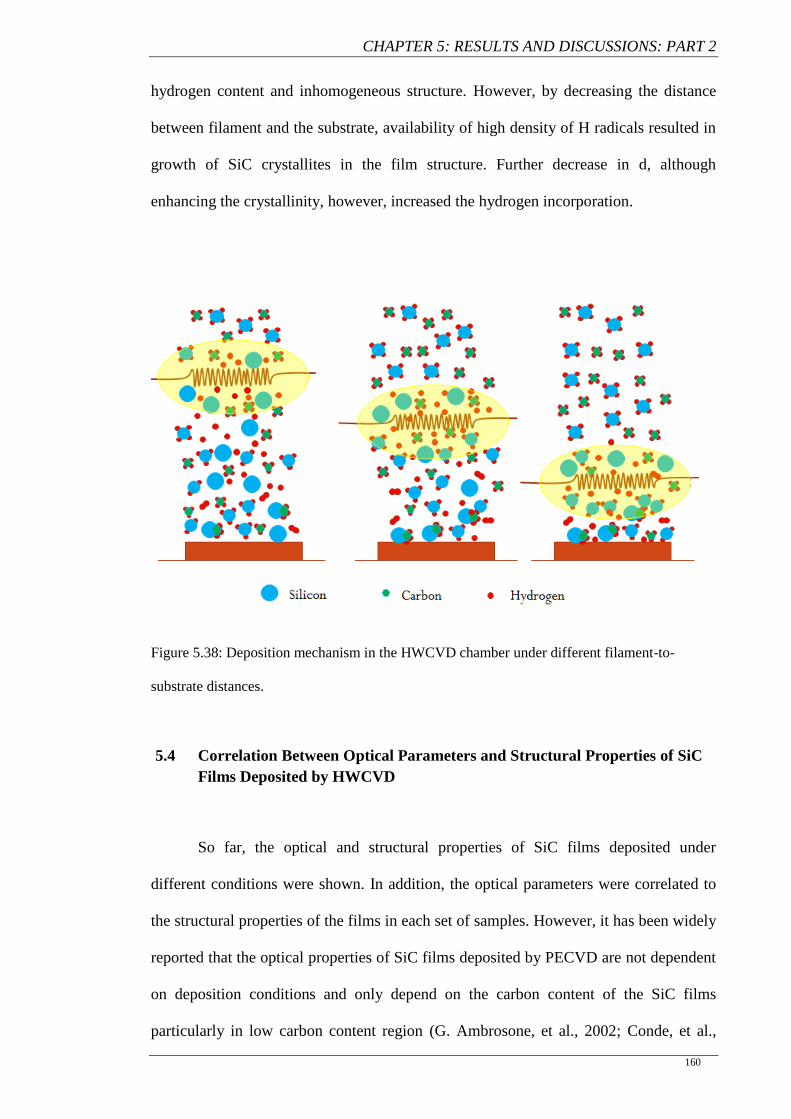
CHAPTER 5: RESULTS AND DISCUSSIONS: PART 2
160
hydrogen content and inhomogeneous structure. However, by decreasing the distance
between filament and the substrate, availability of high density of H radicals resulted in
growth of SiC crystallites in the film structure. Further decrease in d, although
enhancing the crystallinity, however, increased the hydrogen incorporation.
Figure 5.38: Deposition mechanism in the HWCVD chamber under different filament-to-
substrate distances.
5.4 Correlation Between Optical Parameters and Structural Properties of SiC
Films Deposited by HWCVD
So far, the optical and structural properties of SiC films deposited under
different conditions were shown. In addition, the optical parameters were correlated to
the structural properties of the films in each set of samples. However, it has been widely
reported that the optical properties of SiC films deposited by PECVD are not dependent
on deposition conditions and only depend on the carbon content of the SiC films
particularly in low carbon content region (G. Ambrosone, et al., 2002; Conde, et al.,
CHAPTER 5: RESULTS AND DISCUSSIONS: PART 2
161
1999; Hartel, 2010; Mastelaro et al., 1996). Nevertheless, in the case of HWCVD SiC
films, there is a lack of comprehensive investigation to establish such a correlation. B.P.
Swain has correlated the increase of band gap of HWCVD a-SiC:H films to the increase
in Si-C bond density. However, the decrease in the size of graphite carbon clusters
resulted in saturation of band gap at higher carbon content (B.P. Swain, 2006a). T. Wu
et al has reported that the volume fraction of Si-phased in SiC films controls the energy
band gap (Wu, 2011). Some other researchers believe that the carbon incorporation in
the SiC film plays a key role in regulation of the band gap (A. S. Kumbhar, et al., 1995;
Mori, Tabata, & Mizutani, 2006; A. Tabata, Kuroda, M., Mori, M., Mizutani, T.,
Suzuoki, Y., 2004). However, sometimes the variation of the energy gap or refractive
index cannot be explained in terms of the carbon content. For example, in nano-
crystalline SiC films the enhancement of energy band gap has been attributed to the
improvement of crystallinity (Mao, et al., 2012; A. Tabata & Mori, 2008).
In this work, the deposition of amorphous and nano-crystalline SiC under
different deposition conditions by HWCVD method was demonstrated. Although there
are many factors affecting energy band gap and refractive index as reported in the
literature and this work, most of the previous reports emphasized the influence of
carbon content. In order to further establish this influence on the optical properties after
establishing that the structural properties of SiC films were not dependent on substrate,
the dependence of optical parameters on the carbon content of SiC films prepared in this
work at various conditions was studied using optical parameters obtained at various
deposition conditions including the parameters obtained in Chapter 4 along with
parameters obtained from reported work in the literature.
Figure 5.39 demonstrates the variation of the energy band gap and refractive
index of the SiC films deposited under various d as a function of G peak position and
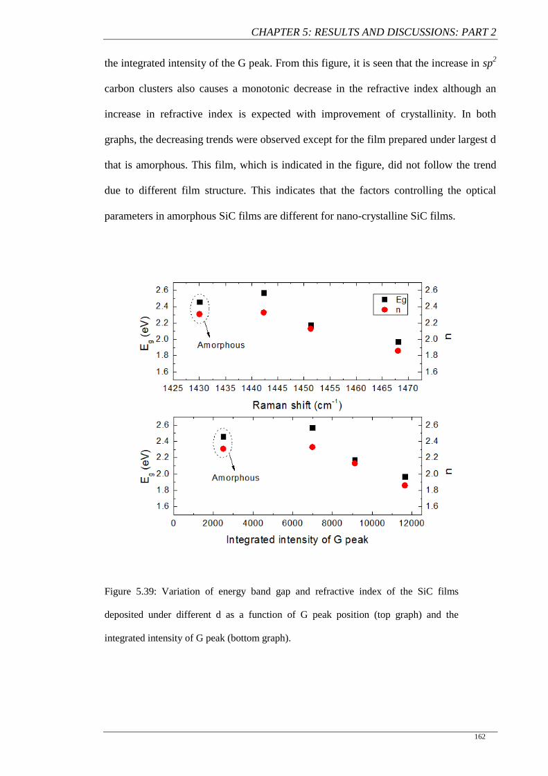
CHAPTER 5: RESULTS AND DISCUSSIONS: PART 2
162
the integrated intensity of the G peak. From this figure, it is seen that the increase in sp2
carbon clusters also causes a monotonic decrease in the refractive index although an
increase in refractive index is expected with improvement of crystallinity. In both
graphs, the decreasing trends were observed except for the film prepared under largest d
that is amorphous. This film, which is indicated in the figure, did not follow the trend
due to different film structure. This indicates that the factors controlling the optical
parameters in amorphous SiC films are different for nano-crystalline SiC films.
Figure 5.39: Variation of energy band gap and refractive index of the SiC films
deposited under different d as a function of G peak position (top graph) and the
integrated intensity of G peak (bottom graph).
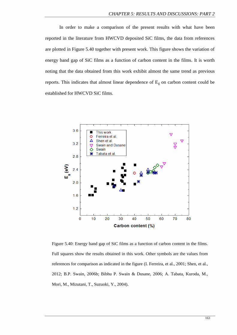
CHAPTER 5: RESULTS AND DISCUSSIONS: PART 2
163
In order to make a comparison of the present results with what have been
reported in the literature from HWCVD deposited SiC films, the data from references
are plotted in Figure 5.40 together with present work. This figure shows the variation of
energy band gap of SiC films as a function of carbon content in the films. It is worth
noting that the data obtained from this work exhibit almost the same trend as previous
reports. This indicates that almost linear dependence of Eg on carbon content could be
established for HWCVD SiC films.
Figure 5.40: Energy band gap of SiC films as a function of carbon content in the films.
Full squares show the results obtained in this work. Other symbols are the values from
references for comparison as indicated in the figure (I. Ferreira, et al., 2001; Shen, et al.,
2012; B.P. Swain, 2006b; Bibhu P. Swain & Dusane, 2006; A. Tabata, Kuroda, M.,
Mori, M., Mizutani, T., Suzuoki, Y., 2004).
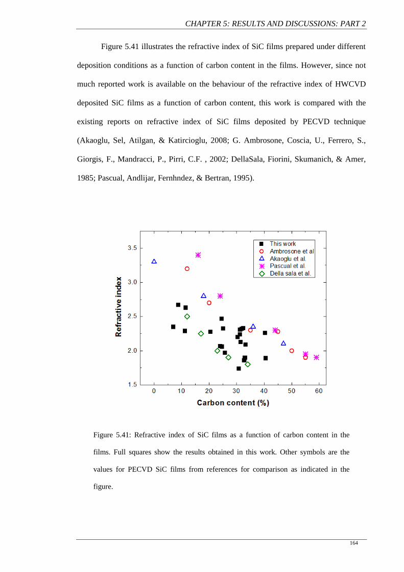
CHAPTER 5: RESULTS AND DISCUSSIONS: PART 2
164
Figure 5.41 illustrates the refractive index of SiC films prepared under different
deposition conditions as a function of carbon content in the films. However, since not
much reported work is available on the behaviour of the refractive index of HWCVD
deposited SiC films as a function of carbon content, this work is compared with the
existing reports on refractive index of SiC films deposited by PECVD technique
(Akaoglu, Sel, Atilgan, & Katircioglu, 2008; G. Ambrosone, Coscia, U., Ferrero, S.,
Giorgis, F., Mandracci, P., Pirri, C.F. , 2002; DellaSala, Fiorini, Skumanich, & Amer,
1985; Pascual, Andlijar, Fernhndez, & Bertran, 1995).
Figure 5.41: Refractive index of SiC films as a function of carbon content in the
films. Full squares show the results obtained in this work. Other symbols are the
values for PECVD SiC films from references for comparison as indicated in the
figure.
CHAPTER 5: RESULTS AND DISCUSSIONS: PART 2
165
From Figure 5.41 it appears that refractive index of SiC films decreases with the
increasing carbon content in the films. The data obtained in this work follow the general
trend in spite of relatively lower values than PECVD deposited SiC films. This is
probably due to the different kinetic mechanism in HWCVD. In HWCVD, because of
lower dissociation of CH4 molecules, usually CHx radicals are produced and
incorporated into the films. Therefore, the presence of many H terminated bonds would
result in less dense films. As a result, in this work, SiC films with slightly lower
refractive index than PECVD SiC films (in the literature) were obtained. However,
refractive index fairly provides an estimation of carbon content in HWCVD SiC films
as suggested in early studies (Bullot & Schmidt, 1987).
5.4 Summary
In this chapter, the effects of two important deposition parameters that is
deposition pressure and filament-to-substrate distance on the growth rate, structural and
optical properties of SiC films were studied. In order to explore the influence of
structural properties on the refractive index, optical energy gap and photoluminescence
properties of deposited films, the dependence of SiC film deposition in HWCVD on c-
Si and glass substrates was also investigated. This is to facilitate the fact that the optical
energy gap and refractive index of the films were derived from the optical transmission
spectra of the films which can only be measured on films on glass substrates.
The results in this chapter show that deposition pressures and filament-to-
substrate distances have strong influence on the growth rate of the SiC films grown by
HWCVD system used in this work. The growth rate of SiC films was reduced
CHAPTER 5: RESULTS AND DISCUSSIONS: PART 2
166
significantly at the critical deposition pressure and filament to substrate distance of 80
Pa and 20 mm respectively, where the film structure reached a transition point of
structural change from nano-crystalline to a totally amorphous structure. It was also
established from the results in this chapter that the formation of a-C:H clusters was
responsible for higher deposition rate at high deposition pressures (above 80 Pa) and
lower filament-to-substrate distances (below 2.0 cm).
The structural properties of SiC films deposited under various deposition
pressures obtained from XRD, Raman and FTIR analysis reveal that the increase in
deposition pressure from 40 to 80 Pa has transformed the structure of the film from a
structure of Si nano-crystallites embedded in Si-rich amorphous SiC film to a nearly
stoichiometric and highly ordered amorphous SiC film structure. Further increase in the
deposition pressure resulted in the formation of a multi-phased film structure consisting
of a-Si:H, a-C:H, and a-SiC with high structural disorder.
The influence of filament-to-substrate distance (d) on structural properties of
SiC films was significant. It was shown that the decrease in d promoted the formation of
nano-crystalline SiC phases and a-C:H clusters in the films as verified by the XRD and
Raman analysis respectively. The Si-C bond density showed no dependence on the
deposition pressure with increasing d from 10 to 20 mm but decreased significantly
when the film structure changed to an amorphous film structure with increase in d to 25
mm. From AES measurement it was revealed that the filament-to-substrate distance had
no important effect on composition of the films.
The Raman scattering and XRD measurements of the films deposited under
various deposition pressures and filament-to-substrate distances were compared for the
films deposited on glass and c-Si substrate. The results confirmed that the structure of
SiC films grown was not dependent on the substrate used for the films and the problem
CHAPTER 5: RESULTS AND DISCUSSIONS: PART 2
167
of relating the structural properties to the optical energy gap and refractive index
obtained only from films deposited on glass substrate can be resolved. To the best of the
author’s knowledge, most reported work on this aspect did not establish the fact that the
structural properties of SiC films grown by HWCVD were independent of substrate
prior to relating the structural properties of the films to the optical properties of the
films which can only be measured on films deposited on transparent substrates.
Optical characterization and analysis of the films deposited under different
deposition pressure showed that the energy gap of the films was largely influenced by
the structural changes in the films. It was established that the energy band gap increases
exponentially with increasing Si-C bond density. A wide band gap of ~2.5 eV was
obtained from a-SiC film deposited at 80 Pa showing that the Si-C bond density was
highest for this film. However, an increase in the deposition pressure resulted in a
continuous decrease in the refractive index of the films, showing that the decrease in the
optical energy gap and refractive index with increasing deposition pressure above 80 Pa
were not mainly influenced by the Si-C bond density in the films. This parallel decrease
in optical energy gap and refractive index with increase in deposition pressure was
attributed to the presence of a-C:H clusters in the film structure. The formation of a-C:H
clusters formed defect states in the forbidden gap of the a-SiC structure at high
pressures which reduced the optical energy gap of the films. The increase in the H
content in a-C:H clusters incorporated in the film structure was responsible for the
further decrease in the refractive index with increasing the deposition pressure although
the Si-C bond density in the films decreased.
Radiative recombination processes in the films has revealed the role of Si
crystallites as radiative recombination centres. The Si-rich SiC films embedded with Si
nano-crystallites showed a room temperature PL emission in the visible range.
CHAPTER 5: RESULTS AND DISCUSSIONS: PART 2
168
Amorphous SiC films deposited under high deposition pressure produced PL emission
peak at lower energies which originated from radiative recombination in the tail states.
The effects of filament-to-substrate distance on optical energy gap, refractive
index and the PL properties of SiC were found to be related to the variation of a-C:H
clusters since these properties were not related to the Si-C bond density in the films
mainly because the films were mainly nano-crystalline in structure. The increase in the
presence of a-C:H clusters at low d led to a decrease in both the optical energy band gap
and refractive index as the a-C:H clusters created defect states and increased the H
content in the SiC film structure. The increase in the H content was mainly in the a-C:H
clusters as reflected by the increase in the slope of C-C bond signature region in the
Raman spectra. From the room temperature PL spectra of the films in this series, it was
revealed that the main radiative recombination processes were contributed by the band-
to-band and band-to-band tail transitions in the amorphous SiC matrix showing that the
a-C:H clusters in the film structure played an important role in the PL properties of the
films as well.
It was established that the growth mechanism of SiC films by HWCVD is
mainly controlled by deposition pressure and filament-to-substrate distance. The
deposition pressure determined the rate of gas phase reactions by controlling the density
and residence time of the radicals in the deposition chamber. On the other hand, the
distance between filament and the substrate governed the flux of energetic H radicals
reaching the growth surface and thus had a great effect on the surface reactions.
Therefore, these two deposition parameters significantly determined the structural
properties of deposited films as well as the deposition rate.
It was shown earlier in this work on the role of Si-C bond density, H content and
the a-C:H clusters presence in controlling the refractive index and the optical energy
CHAPTER 5: RESULTS AND DISCUSSIONS: PART 2
169
gap of the films. However, the AES results showed that that the carbon content in the
film was the most important overall parameter that controlled the refractive index and
optical energy gap of SiC films deposited by the HWCVD in this work. The results in
this work showed that increase in the carbon content has increased optical energy band
gap of SiC films but showed a reversed trend on the refractive index. The C atoms in the
film structure were either bonded to Si atoms forming SiC phases or bonded to C or H
atoms forming a-C:H clusters. Therefore, even though the bonding configuration of
carbon atoms incorporated in the film structure had control on these optical parameters,
the actual carbon content in the film structure played a major role in controlling these
two optical parameters as established in this work. This is the first time within the
author’s knowledge that it is reported that the C content in SiC films deposited by
HWCVD is the most important structural parameter that controls the optical energy gap
and refractive index of the films.

CHAPTER 6: CONCLUSIONS
170
CHAPTER 6
Conclusions
and
Suggestions For Future
Works
CHAPTER 6: CONCLUSIONS
171
6.1 Conclusions
In this work, a home-built hot-wire chemical vapour deposition system was
successfully utilized to grow multi-phased silicon carbide thin films from pure silane
and methane gases without hydrogen dilution. In the first part of this work, the SiC
films were only grown on crystalline silicon substrates (c-Si) and the influence of
precursor gas concentration on chemical bonding, crystallinity and elemental
composition properties of the films were studied. The structural properties of the films
were analyzed from the Fourier transform infra-red (FTIR), Raman scattering and X-ray
diffraction (XRD) spectroscopy measurements. Auger Electron Spectroscopy (AES)
depth profiling measurement was done on these films to study the elemental
composition distribution within the films. The precursor gas concentration was varied
by depositing two series of films where the first series of films consisted of films
deposited at different methane (CH4) flow-rates with the silane (SiH4) flow-rate fixed at
SiH4 starving condition with flow-rate of 0.5 and 1 standard cubic cm (sccm), and the
second series of films deposited at different total gas partial pressures with the SiH4 to
CH4 flow-rate ratio fixed at 1:20. Two sets of films were deposited for the second series
of films where the deposition pressure was fixed equal to the total gas partial pressure
and 80 Pa for the first and second set of films respectively. In the second part of this
work, the films were deposited simultaneously on both glass and c-Si substrates. The
effects of deposition pressure with the SiH4 to CH4 flow-rates fixed and substrate to
filament distance on the structural and optical properties of films were investigated. The
deposition pressure controlled the residence time of precursor molecules in the reactor
and the substrate to filament distance determined the energy of the radicals reaching the
growth sites and therefore directly influenced surface reactions, which controlled
incorporation of atoms into the film structure. Raman scattering and XRD spectroscopy
CHAPTER 6: CONCLUSIONS
172
measurements were done on films deposited on both c-Si and glass substrates and the
results were used to show that the structural properties of these films were not substrate
dependent. AES depth profiling, FTIR spectroscopy, field emission scanning electron
microscopy (FESEM) and photoluminescence (PL) measurements were done only on
films on c-Si substrates. These results were used to relate the structural properties to the
optical properties of the SiC films and determine the important structural parameters,
which can be used to control the optical properties of the films. Finally, the growth
mechanism of SiC films deposited by the HWCVD system used in this work was
analyzed.
High quality SiC thin films with high deposition rate has been successfully
grown using the home-built HWCVD system in Low Dimensional Materials Research
Centre, University of Malaya. The highest growth rate of the SiC films achieved in this
work, which is close to 1.8 nm/s is higher than the growth rates of SiC films reported in
the literature for films grown by HWCVD, PECVD or various sputtering techniques.
The results from this study showed that lower CH4 gas flow-rate in silane
starving condition was more favourable for the formation of SiC films with high density
of Si-C bonds. The high density Si-C bond concentration was an important factor
contributing to the formation of SiC nano-crystallites deposited at low CH4 flow rate in
this work, where SiC films were deposited by HWCVD without hydrogen dilution. In
most reported works on SiC deposition using a similar technique, hydrogen dilution has
been established to be necessary for the formation of nano-crystalline phase in SiC
films. Thus, it was established here that the formation of SiC crystallites can be
manipulated by controlling the CH4 to SiH4 flow rate ratio in SiH4 starving condition
where the silane flow-rate did not exceed 1 sccm.
CHAPTER 6: CONCLUSIONS
173
The formation of SiC phases in the film structure was demonstrated to be more
favourable at deposition pressure higher than the total gas partial pressure, showing that
increase in residence time of the precursor gas molecules in the reaction chamber was
an important factor for Si-C bond formation. However, formation of high Si-C bond
density at low total gas partial pressure was required to form nano-crystalline SiC phase
in the films. In the initial part of this work, it was realized that an optimum total gas
partial pressure is required for the formation of SiC nano-crystalline phases in the films.
Low total gas partial pressure and longer residence time of the precursor molecules in
the reactor were shown to be necessary for the formation of nano-crystalline SiC phases
in the film structure. This work also established that nano-crystalline SiC film structure
can be grown at much higher CH4 to SiH4 flow-rate ratio than those reported by other
research groups under similar conditions using HWCVD.
The results in this work showed that at fixed SiH4 and CH4 flow-rates, the film
structure transformed from a structure of nc-Si phase embedded within an a-SiC phase
to a nearly stoichiometric and highly ordered a-SiC at an optimum deposition pressure.
Deposition pressure above this optimum pressure was shown to result in the formation
of multi-phased film structure consisting of a-Si:H, a-C:H, and a-SiC with high
structural disorder.
The influence of filament-to-substrate distance (d) on structural properties of
SiC films was significant. It was shown that the decrease in d promoted the formation of
nano-crystalline SiC phases and a-C:H clusters in the film structure. The Si-C bond
density was not dependent on d when the film structure was nano-crystalline in structure
but at large d, the Si-C bond density was shown to decrease significantly and as
demonstrated above this consistently led to the formation of an amorphous film
structure
CHAPTER 6: CONCLUSIONS
174
Comparison of the Raman scattering spectroscopy and XRD results on the films
deposited under various deposition pressure and filament-to-substrate distance on both
glass and c-Si substrate verified that the structure of SiC films grown was not dependent
on the substrate used for the films. This is an important requirement to correlate the
optical energy gap and refractive index of the films, which were measured on films
deposited on glass substrates only with the structural properties especially when
characterization could only be done on films deposited on c-Si substrates only. To the
best of the author’s knowledge, most reported work on this aspect did not establish the
fact that the structural properties of SiC films grown by HWCVD were independent of
substrate prior to relating the structural properties of the films to the optical properties
of the films.
Optical energy gap and refractive index of SiC films are important parameters
for application of this material in opto-electronic devices. In this work, it was
established that these parameters, which were determined from the optical transmission
spectra of the films, were strongly affected by the structural changes in the films. The
optical energy band gap of the a-SiC films showed significant dependence on the Si-C
bond density in the film structure. The largest optical band gap of ~2.5 eV achieved in
this work was obtained from a-SiC film with the highest Si-C bond density deposited at
the optimum deposition pressure. Increase in deposition pressure above the optimum
pressure was demonstrated to produce a parallel decrease in the optical energy gap and
refractive index and the presence of a-C:H clusters in the film structure was also shown
to be responsible for this trend. The changes in the optical energy gap and refractive
index due to the increased presence of a-C:H clusters was shown to have a more
dominant effect in nano-crystalline SiC films deposited at different d where the Si-C
bond density did not show much variation. The increase in the presence of a-C:H
clusters at low d and high deposition pressure led to a decrease in both the optical
CHAPTER 6: CONCLUSIONS
175
energy band gap and refractive index as the a-C:H clusters created defect states and
increased the H content in the SiC film structure regardless of the structure of the film,
whether it was amorphous or nano-crystalline. The results in this work also revealed
that the PL emission from the SiC films was the result of band-to-band transition and
radiative recombination processes occurring in the band tail states of the amorphous SiC
matrix. Thus it was established that SiC phases and the a-C:H clusters in the film
structure played important roles in the PL emission of the films.
The AES results from this work showed that increase in the carbon content
increased optical energy band gap of SiC films but showed a reversed trend on the
refractive index. This nicely complemented the role of Si-C bond density and a-C:H
clusters in controlling both these parameters as explained above since the C atoms in the
film structure were either bonded to Si atoms forming SiC phases or bonded to C or H
atoms forming a-C:H clusters. Therefore, naturally the amount of carbon atoms
incorporated in the film structure can be the main parameter used to control these
optical parameters. This is the first time within the author’s knowledge that this
explanation on how the optical band gap and refractive index of SiC films deposited by
HWCVD from the discharge of pure SiH4 and CH4 gases without hydrogen dilution is
reported.
The deposition mechanisms of the SiC films grown by HWCVD in this work
have been established from the analysis on the variation of growth rates, bonding
properties and elemental composition of the films with the various growth parameters
studied. Generally, the concentration of precursor gases in the chamber and residence
time of the precursor gas molecules and growth radicals in the reaction chamber showed
strong influence on the growth rate of the films. The concentration of precursor gases in
the chamber and residence time was controlled by the CH4 flow-rate, total gas partial
CHAPTER 6: CONCLUSIONS
176
pressure and the deposition pressure in this work. The deposition parameters were
responsible for the increased presence of C and H atoms reaching the growth sites. The
H atoms created nucleation sites and the C atoms enhanced the formation of SiC and a-
C:H phases in the film structure promoting film growth. The filament temperature used
in this work effectively dissociated the SiH4 gas in the vicinity of the filament but did
not contribute much to the number of C atoms reaching the growth sites. The filament to
substrate distance on the other hand governed the flux of energetic H radicals reaching
the growth surface and thus contributed significantly to the surface reactions, which
incorporated atoms into the film structure. Therefore, these two deposition parameters
significantly influenced the structural properties of deposited films as well as the
deposition rate. Another significant result produced in this work is the transformation of
the film structure from amorphous to nano-crystalline phase, which was shown to
produce a significant drop in the growth rate. Dominant H etching effect at this critical
CH4 flow-rate with the SiH4 flow-rate fixed at SiH4 starving condition and filament-to-
substrate distance produced the low growth rate.
6.3 Recommendations For Future Work
The results in this work can be strengthened further if further investigations
which are not within the scope of this work are done. A high resolution transmission
electron microscopy (HRTEM) analysis can be more conclusive in confirming the
presence of the various amorphous and crystalline phases present in the film structure.
This measurement is capable of determining the size as well as the polytypes of SiC
nano-crystallites present. The energy dispersive X-ray (EDX) analysis equipped with
CHAPTER 6: CONCLUSIONS
177
HRTEM system can also provide a precise record of the elemental composition of the
different phases in the film structure.
Better understanding of the gas phase reactions and the main radicals and
precursors contributing to the growth of the SiC films can be achieved if in-situ gas-
phase diagnostic technique such as mass spectroscopy is available during the film
growth process. Consequently, the growth mechanism responsible for the growth of SiC
thin film by HWCVD can be clearly understood. As a result, a precise control of the
structure of the films under different deposition conditions can be made possible.
Further studies on the effect of other deposition parameters of HWCVD system
are recommended. Since the hot filament plays the most important role in the deposition
of SiC films by HWCVD, it would be beneficial to study the effect of the use of
different filament material, filament geometry and filament layout in relation to the
properties of the SiC films, The influence of filament temperature on the film properties
is an important area of study to pursue in future studies as dissociation of CH4 gas can
be enhanced by the filament temperature which may result in the formation of other SiC
polytypes.
Finally, the application of amorphous and nano-crystalline SiC films as a
window layer in silicon solar cells should be investigated and tested in future works.
This would further enhance the capability of the home-built HWCVD system used in
this work to produce high quality SiC films for this purpose. Additionally, other
applications on the SiC material produced by this simple and cost-effective home-built
HWCVD system can be tested if mechanical, bio-compatibility and electrical properties
of the films are studied. These properties of SiC have generated a lot of interest in

CHAPTER 6: CONCLUSIONS
178
studying the material as a coating material, in medical applications, and electronic
devices.
REFERENCES
179
REFERENCES
Akaoglu, B., Sel, K., Atilgan, I., & Katircioglu, B. (2008). Carbon content influence on
the optical constants of hydrogenated amorphous silicon carbon alloys. Optical
Materials, 30, 1257-1267.
Ambrosone, G., Basa, D. K., Coscia, U., & Passacantando, M. (2012). Evolution of
structural and optical properties of nanostructured silicon carbon films deposited
by plasma enhanced chemical vapour deposition. Thin Solid Films, 520(15),
4875-4879.
Ambrosone, G., Coscia, U., Lettieri, S., Maddalena, P., Noce, M. D., Ferrero, S., et al.
(2006). Silicon–carbon films deposited at low substrate temperature. Journal of
Non-Crystalline Solids, 352(9–20), 1371-1375.
Ambrosone, G., Coscia, U., Lettieri, S., Maddalena, P., Privato, C., & Ferrero, S.
(2002). Hydrogenated amorphous silicon carbon alloys for solar cells. Thin Solid
Films, 403-404, 349-353.
Ambrosone, G., Coscia, U., Ferrero, S., Giorgis, F., Mandracci, P., Pirri, C.F. . (2002).
Structural and optical properties of hydrogenated amorphous silicon carbon
alloys grown by plasma-enhanced chemical vapour deposition at various rf
powers. Philos. Mag. B 82, 35.
Azis, A. (2012). Hot-wire plasma enhanced chemical vapour deposition system for
preparation of silicon carbide thin films University of Malaya, Kuala Lumpur.
Bhusari, D. M., & Kshirsagar, S. T. (1993). Effect of radio-frequency power and
substrate temperature on properties of hot-plasma-box glow-discharge-deposited
hydrogenated amorphous silicon carbon alloys. Journal of Applied Physics,
73(4), 1743-1749.
Bullot, J., & Schmidt, M. P. (1987). Physics of Amorphous Silicon–Carbon Alloys.
physica status solidi (b), 143(2), 345-418.
Chakraborty, K., & Das, D. (2006). Structural studies on the microcrystallization of
Si:H network developed by hot-wire CVD. Solar Energy Materials and Solar
Cells, 90(7–8), 849-863.
Chang, P.-K., Hsu, W.-T., Hsieh, P.-T., Lu, C.-H., Yeh, C.-H., & Houng, M.-P. (2012).
Improved stability of amorphous silicon solar cells with p-type nanocrystalline
silicon carbide window layer. Thin Solid Films, 520(7), 3096-3099.
Chen, T., Huang, Y., Dasgupta, A., Luysberg, M., Houben, L., Yang, D., et al. (2012).
Microcrystalline silicon carbide window layers in thin film silicon solar cells.
Solar Energy Materials and Solar Cells, 98(0), 370-378.
Chen, T., Huang, Y., Yang, D., Carius, R., & Finger, F. (2010). Microcrystalline silicon
thin film solar cells with microcrystalline silicon carbide window layers and
silicon absorber layers both prepared by Hot-Wire CVD. physica status solidi
(RRL) – Rapid Research Letters, 4(3-4), 61-63.
REFERENCES
180
Chen, T., Huang, Y., Yang, D., Carius, R., & Finger, F. (2011). Development of
microcrystalline silicon carbide window layers by hot-wire CVD and their
applications in microcrystalline silicon thin film solar cells. Thin Solid Films,
519(14), 4523-4526.
Chen, T., Yang, D., Carius, R., & Finger, F. (2010). Highly Conductive p-Type Silicon
Carbon Alloys Deposited by Hot-Wire Chemical Vapor Deposition. japanese
Journal of Applied Physics, 49, 041303.
Cheng, Q., & et al. (2008). High-rate, low-temperature synthesis of composition
controlled hydrogenated amorphous silicon carbide films in low-frequency
inductively coupled plasmas. Journal of Physics D: Applied Physics, 41(5),
055406.
Cheng, Q., Eugene Tam, Shuyan Xub and Kostya (Ken) Ostrikov. (2010). Si quantum
dots embedded in an amorphous SiC matrix: nanophase control by non-
equilibrium plasma hydrogenation. Nanoscale, 2, 594-600.
Cheng, Q., Xu, S. . (2007). Low-temperature synthesis of homogeneous nanocrystalline
cubic silicon carbide films. Journal of Applied Physics, 102(5), 056101.
Chevaleevski, O., Myong, S. Y., & Lim, K. S. (2003). Spin defects and transport in
hydrogenated nanocrystalline silicon carbide films produced by photo-CVD
technique. Solid State Communications, 128(9–10), 355-358.
Chew, K., Rusli, Yoon, S. F., Ahn, J., Ligatchev, V., Teo, E. J., Osipowicz, T., Watt, F.
(2002). Hydrogenated amorphous silicon carbide deposition using electron
cyclotron resonance chemical vapor deposition under high microwave power
and strong hydrogen dilution. Journal of Applied Physics, 92(5), 2937-2941.
Comninellis, C., & Chen, G. (2009). Electrochemistry for the Environment: Springer
New York.
Compagnini, G., Foti, G., & Makhtari, A. (1998). Vibrational analysis of compositional
disorder in amorphous silicon carbon alloys. EPL (Europhysics Letters), 41(2),
225.
Conde, J. P., Chu, V., Silva, M. F. d., Kling, A., Dai, Z., Soares, J. C., et al. (1999).
Optoelectronic and structural properties of amorphous silicon–carbon alloys
deposited by low-power electron-cyclotron resonance plasma-enhanced
chemical-vapor deposition. Journal of Applied Physics, 85(6), 3327-3338.
Coscia, U., Ambrosone, G., & Basa, D. K. (2008). Room temperature visible
photoluminescence of silicon nanocrystallites embedded in amorphous silicon
carbide matrix. Journal of Applied Physics, 103(6), 063507.
Dasgupta, A., Ghosh, S., Kshirsagar, S. T., & Ray, S. (1997). Effect of chamber
pressure on p-type μc-SiC:H thin films prepared by photo-CVD. Thin Solid
Films, 295(1-2), 37-42.
Davis, E. A., Piggins, N., & Bayliss, S. C. (1987). Optical properties of amorphous SiN
x (:H) films. Journal of Physics C: Solid State Physics, 20(27), 4415.
REFERENCES
181
DellaSala, D., Fiorini, P., Skumanich, A., & Amer, N. M. (1985). Gap state
spectroscopy in a-Si1-xCx:H alloys Journal of Non-Crystalline Solids, 77-78,
853.
Dhanaraj, G., Chen, Y., Chen, H., Cai, D., Zhang, H., & Dudley, M. (2007). Chemical
Vapor Deposition of Silicon Carbide Epitaxial Films and Their Defect
Characterization. Journal of Electronic Materials, 36(4), 332-339.
Doyle, J., Robertson, R., Lin, G. H., He, M. Z., & Gallagher, A. (1988). Production of
high-quality amorphous silicon films by evaporative silane surface
decomposition. Journal of Applied Physics, 64(6), 3215-3223.
Duan, H. L., & Bent, S. F. (2005). The influence of filament material on radical
production in hot wire chemical vapor deposition of a-Si:H. Thin Solid Films,
485(1–2), 126-134.
Duan, H. L., Zaharias, G. A., & Bent, S. F. (2002). Detecting reactive species in hot
wire chemical vapor deposition. Current Opinion in Solid State and Materials
Science, 6(5), 471-477.
El Khakani, M. A., Guay, D., Chaker, M., & Feng, X. H. (1995). Composition and
thermal-annealing-induced short-range ordering changes in amorphous
hydrogenated silicon carbide films as investigated by extended x-ray-absorption
fine structure and infrared absorption. Physical Review B, 51(8), 4903-4914.
Ellison, A., Magnusson, B., Hemmingsson, C., Magnusson, W., Iakimov, T., Storasta,
L., et al. (2000). HTCVD growth of semi-insulating 4H-SiC crystals with low
defect density. MRS Online Proceedings Library, 640, null-null.
Ellison, A., Zhang, J., Peterson, J., Henry, A., Wahab, Q., Bergman, J. P., et al. (1999).
High temperature CVD growth of SiC. Materials Science and Engineering: B,
61–62(0), 113-120.
Feenstra, K. F., Schropp, R. E. I., & Van der Weg, W. F. (1999). Deposition of
amorphous silicon films by hot-wire chemical vapor deposition. Journal of
Applied Physics, 85(9), 6843-6852.
Feng, S. H., & Chen, J. S. (2002). Frontiers of Solid State Chemistry: Proceedings of
the International Symposium on Solid State Chemistry in China, Changchun,
China, 9-12 August, 2002: World Scientific.
Feng, Z. C. (2004). SiC Power Materials: Devices and Applications: Springer.
Feng, Z. C. (2006). Optical properties of cubic SiC grown on Si substrate by chemical
vapor deposition. Microelectronic Engineering, 83(1), 165-169.
Ferrari, A. C., & Robertson, J. (2000). Interpretation of Raman spectra of disordered
and amorphous carbon. Physical Review B, 61(20), 14095-14107.
Ferrari, A. C., & Robertson, J. (2004). Raman spectroscopy of amorphous,
nanostructured, diamond–like carbon, and nanodiamond. Phil. Trans. R. Soc.
Lond. A, 362(1824), 2477-2512.
REFERENCES
182
Ferraro, J. R., Nakamoto, K., & Brown, C. W. (2003). Chapter 1 - Basic Theory
Introductory Raman Spectroscopy (Second Edition) (pp. 1-94). San Diego:
Academic Press.
Ferreira, I., Cabrita, A., Fortunato, E., Martins, R. (2002). Composition and structure of
silicon-carbide alloys obtained by hot wire and hot wire plasma assisted
techniques. Vacuum, 64(3-4), 261-266.
Ferreira, I., Costa, M. E. V., Pereira, L., Fortunato, E., Martins, R., Ramos, A. R., et al.
(2001). Silicon carbide alloys produced by hot wire, hot wire plasma-assisted
and plasma-enhanced CVD techniques. Applied Surface Science, 184(1-4), 8-19.
Ferreira, I., Fernandes, B., & Martins, R. (1999). Nanocrystalline silicon carbon doped
films prepared by hot wire technique. Vacuum, 52(1–2), 147-152.
Finger, F., Astakhov, O., Bronger, T., Carius, R., Chen, T., Dasgupta, A., et al. (2009).
Microcrystalline silicon carbide alloys prepared with HWCVD as highly
transparent and conductive window layers for thin film solar cells. Thin Solid
Films, 517(12), 3507-3512.
Fissel, A. (2003). Artificially layered heteropolytypic structures based on SiC
polytypes: molecular beam epitaxy, characterization and properties. Physics
Reports, 379(3–4), 149-255.
Friedrichs, P., Kimoto, T., Ley, L., & Pensl, G. (2011). Silicon Carbide: Wiley.
Gallagher, A. (2001). Some physics and chemistry of hot-wire deposition. Thin Solid
Films 395, 25-28.
George, V. C., Das, A., Roy, M., Dua, A. K., Raj, P., & Zahn, D. R. T. (2002). Bias
enhanced deposition of highly oriented β-SiC thin films using low pressure hot
filament chemical vapour deposition technique. Thin Solid Films, 419(1–2),
114-117.
Gogoi, P., Jha, H. S., & Agarwal, P. (2010). High band gap nanocrystallite embedded
amorphous silicon prepared by hotwire chemical vapour deposition. Thin Solid
Films, 518(23), 6818-6828.
Goh, B. T. (2012). Layer-by-layer plasma enhanced chemical vapour deposition of
nanocrystalline silicon thin films. University of Malaye, Kuala lumpur.
Griffiths, P., & De Haseth, J. A. (2007). Fourier Transform Infrared Spectrometry: John
Wiley & Sons.
Guo, Y. P., Zheng, J. C., Wee, A. T. S., Huan, C. H. A., Li, K., Pan, J. S., et al. (2001).
Photoluminescence studies of SiC nanocrystals embedded in a SiO2 matrix.
Chemical Physics Letters, 339(5–6), 319-322.
Guruvenket, S., Azzi, M., Li, D., Szpunar, J. A., Martinu, L., Klemberg-Sapieha, J. E.
(2010). Structural, mechanical, tribological, and corrosion properties of a-SiC:H
coatings prepared by PECVD. Surface and Coating Technology, 204(21-22),
3358-3365.
Harris, G. L. (1995). Properties of Silicon Carbide: Inst of Engineering & Technology.
REFERENCES
183
Hartel, A. M., Künle, M., Löper, P., Janz, S., Bett, A. W. (2010). Amorphous SixC1-x:H
single layers before and after thermal annealing: Correlating optical and
structural properties. Solar Energy Materials and Solar Cells, 94(11), 1942-
1946.
Heintze, M., Zedlitz, R., Wanka, H. N., & Schubert, M. B. (1996). Amorphous and
microcrystalline silicon by hot wire chemical vapor deposition. Journal of
Applied Physics, 79(5), 2699-2706.
Hiromasa, O., Takahiro, H., Tetsuya, M., Hiroaki, K., & Kiyoshi, Y. (2011). Low-
temperature synthesis of microcrystalline 3C-SiC film by high-pressure
hydrogen-plasma-enhanced chemical transport. Journal of Physics D: Applied
Physics, 44(23), 235202.
Holt, J. K., Swiatek, M., Goodwin, D. G., Muller, R. P., Goddard Iii, W. A., & Atwater,
H. A. (2001). Gas phase and surface kinetic processes in polycrystalline silicon
hot-wire chemical vapor deposition. Thin Solid Films, 395(1–2), 29-35.
Hori, M., & Goto, T. (2002). Measurement techniques of radicals, their gas phase and
surface reactions in reactive plasma processing. Applied Surface Science, 192(1–
4), 135-160.
Hoshide, Y., Komura, Y., Tabata, A., Kitagawa, A., Kondo, A. (2009). Importance of
H2 gas for growth of hot-wire CVD nanocrystalline 3C-SiC from SiH4/CH4/H2.
Thin Solid Films, 517(12), 3520-3523.
Hoshide, Y., Tabata, A., Kitagawa, A., Kondo, A. (2009). Preparation of n-type
nanocrystalline 3C-SiC films by hot-wire CVD using N2 as doping gas. Thin
Solid Films, 517(12), 3524-3527.
Hu, Z., et al. (2004). Amorphous silicon carbide films prepared by H2 diluted silane-
methane plasma. Journal of Crystal Growth, 264, 7-12.
Huang, S. M., et al. (2002). Ultraviolet and visible Raman spectroscopy characterization
of diamond–like carbon film growth by pulsed laser deposition. Applied Physics
A, 74(4), 519-523.
Itoh, T., Fukunaga, K., Katoh, Y., Fujiwara, T., & Nonomura, S. (2002). Doping of a-
SiCX:H films including μc-Si:H by hot-wire CVD and their application as a wide
gap window for heterojunction solar cells. Solar Energy Materials and Solar
Cells, 74(1-4), 379-385.
Itoh, T., Katoh, Y., Fujiwara, T., Fukunaga, K., Nonomura, S., & Nitta, S. (2001).
Preparation of silicon-carbon alloy films by hot-wire CVD and their properties.
Thin Solid Films, 395(1-2), 240-243.
Jadkar, S. R., Sali, J. V., Funde, A. M., Ali Bakr, N., Vidyasagar, P. B., Hawaldar, R.
R., et al. (2007). Deposition of hydrogenated amorphous silicon (a-Si:H) films
by hot-wire chemical vapor deposition (HW-CVD) method: Role of substrate
temperature. Solar Energy Materials and Solar Cells, 91(8), 714-720.
Jadkar, S. R., Sali, J. V., Musale, D. V., Kshirsagar, S. T., & Takwale, M. G. (2002).
Influence of silane flow on structural, optical and electrical properties of a-Si:H
REFERENCES
184
thin films deposited by hot wire chemical vapor deposition (HW-CVD)
technique. Solar Energy Materials and Solar Cells, 71(2), 153-167.
Jha, H. S., Singh, M., Yadav, A., Lalhriatzuala, Deva, D., & Agarwal, P. (2012).
Nanocrystalline cubic silicon carbide thin films for the window layer of solar
cells deposited by hot wire CVD. 85493D-85493D.
Kaneko, T., Nemoto, D., Horiguchi, A., Miyakawa, N. (2005). FTIR analysis of a-
SiC:H films grown by plasma enhanced CVD. Journal of Crystal Growth,
275(1–2), e1097-e1101.
Karch, K., Bechstedt, F., Pavone, P., & Strauch, D. (1996). Pressure-dependent
properties of SiC polytypes. Physical Review B, 53(20), 13400-13413.
Kerdiles, S. (2000). Low temperature deposition of nanocrystalline silicon carbide thin
films. Applied Physics Letters, 76(17), 2373.
Kerdiles, S., Madelon, R., & Rizk, R. (2001). Spectroscopic ellipsometry analysis of
nanocrystalline silicon carbide obtained at low temperature. Applied Surface
Science, 184(1–4), 150-155.
Kerdiles, S., Rizk, R., ourbilleau, F., P rez-Rodr guez, ., arrido, B., onz lez-
Varona, O., et al. (2000). Low temperature direct growth of nanocrystalline
silicon carbide films. Materials Science and Engineering: B, 69–70(0), 530-535.
Kessels, W. M. M., Hoefnagels, J. P. M., van den Oever, P. J., Barrell, Y., & van de
Sanden, M. C. M. (2003). Temperature dependence of the surface reactivity of
SiH3 radicals and the surface silicon hydride composition during amorphous
silicon growth. Surface Science, 547(3), L865-L870.
King, S. W., French, M., Bielefeld, J., & Lanford, W. A. (2011). Fourier transform
infrared spectroscopy investigation of chemical bonding in low-k a-SiC:H thin
films. Journal of Non-Crystalline Solids, 357(15), 2970-2983.
Klein, S., Dasgupta, A., Finger, F., Carius, R., & Bronger, T. (2008). Electronic
properties of low temperature microcrystalline silicon carbide prepared by Hot
Wire CVD. Thin Solid Films, 516(5), 630-632.
Klein, S., Finger, F., Carius, R., & Stutzmann, M. (2005). Deposition of
microcrystalline silicon prepared by hot-wire chemical-vapor deposition: The
influence of the deposition parameters on the material properties and solar cell
performance. Journal of Applied Physics, 98(2), 024905.
Klug, H. P., & Alexander, L. E. (1974). X-ray diffraction procedures for polycrystalline
and amorphous materials. New York: Wiley.
Komiyama, J., Abe, Y., Suzuki, S., Kita, T., & Nakanishi, H. (2005). Schottky diode
characteristics of 3C-SiC grown on a Si substrate by vapor phase epitaxy.
Journal of Crystal Growth, 275(1–2), e1001-e1006.
Komura, Y., Tabata, A., Narita, T., Kondo, A. (2008). Influence of gas pressure on low-
temperature preparation and film properties of nanocrystalline 3C-SiC thin films
by HW-CVD using SiH4/CH4/H2 system. Thin Solid Films, 516(5), 633-636.
REFERENCES
185
Kordina, O., Hallin, C., Ellison, A., Bakin, A. S., Ivanov, I. G., Henry, A., et al. (1996).
High temperature chemical vapor deposition of SiC. Applied Physics Letters,
69(10), 1456-1458.
Kumbhar, A. A., Dusane, R. O., Bauer, S., & Schröder, B. (1998). Micro-crystalline
phase formation in hot wire deposited Si:C:H alloy films from pure methane and
silane mixtures. Journal of Non-Crystalline Solids, 227-230, Part 1(0), 452-455.
Kumbhar, A. S., Bhusari, D. M., & Kshirsagar, S. T. (1995). Growth of clean
amorphous silicon-carbon alloy films by hot-filament assisted chemical vapor
deposition technique. Applied Physics Letters, 66, 1741.
Lee, M.-S., & Bent, S. F. (2000). Temperature effects in the hot wire chemical vapor
deposition of amorphous hydrogenated silicon carbon alloy. Journal of Applied
Physics, 87(9), 4600-4610.
Lim, K. S., & Shevaleevskiy, O. (2008). Nanocrystalline silicon carbide films for solar
photovoltaics: The role of dangling-bond defects. Pure and Applied Chemistry,
80(10), 2141.
Mahan, A. H. (2003). Hot wire chemical vapor deposition of Si containing materials for
solar cells. Solar Energy Materials and Solar Cells, 78(1–4), 299-327.
Mahan, A. H., Carapella, J., Nelson, B. P., Crandall, R. S., & Balberg, I. (1991).
Deposition of device quality, low H content amorphous silicon. Journal of
Applied Physics, 69(9), 6728-6730.
Mahan, A. H., Nelson, B. P., Salamon, S., & Crandall, R. S. (1991). Deposition of
device quality, low H content a-Si:H by the hot wire technique. Journal of Non-
Crystalline Solids, 137–138, Part 2(0), 657-660.
Manifacier, J. C., Gasiot, J., & Fillard, J. P. (1976). A simple method for the
determination of the optical constants n, k and the thickness of a weakly
absorbing thin film. Journal of Physics E: Scientific Instruments, 9(11), 1002.
Mao, H.-Y., Wuu, D.-S., Wu, B.-R., Lo, S.-Y., Hsieh, H.-Y., & Horng, R.-H. (2012).
Hot-wire chemical vapor deposition and characterization of p-type
nanocrystalline SiC films and their use in Si heterojunction solar cells. Thin
Solid Films, 520(6), 2110-2114.
Martin, I. T., Teplin, C. W., Doyle, J. R., Branz, H. M., & Stradins, P. (2010). Physics
and chemistry of hot-wire chemical vapor deposition from silane: Measuring and
modeling the silicon epitaxy deposition rate. Journal of Applied Physics, 107(5),
054906.
Mastelaro, V., Flank, A. M., Fantini, M. C. A., Bittencourt, D. R. S., Carreno, M. N. P.,
& Pereyra, I. (1996). On the structural properties of a-Si1-xCx :H thin films.
Journal of Applied Physics, 79(3), 1324-1329.
Matsuda, A. (2004). Microcrystalline silicon.: Growth and device application. Journal
of Non-Crystalline Solids, 338–340(0), 1-12.
REFERENCES
186
Matsumura, H. (1998). Formation of Silicon-Based Thin Films Prepared by Catalytic
Chemical Vapor Deposition (Cat-CVD) Method. Japanese Journal of Applied
Physics, 37, 3175.
Matsumura, H., & Ihara, H. (1988). Catalytic chemical vapor deposition method to
prepare high quality hydro-fluorinated amorphous silicon. Journal of Applied
Physics, 64(11), 6505-6509.
Matsumura, H., Umemoto, H., Izumi, A., & Masuda, A. (2003). Recent progress of Cat-
CVD research in Japan—bridging between the first and second Cat-CVD
conferences. Thin Solid Films, 430(1–2), 7-14.
Matsumura, H., Umemoto, H., & Masuda, A. (2004). Cat-CVD (hot-wire CVD): how
different from PECVD in preparing amorphous silicon. Journal of Non-
Crystalline Solids, 338–340(0), 19-26.
Miyajima, S., Irikawa, J., Yamada, A., & Konagai, M. (2010). High-quality
nanocrystalline cubic silicon carbide emitter for crystalline silicon
heterojunction solar cells. Applied Physics Letters, 97(2), 023504.
Miyajima, S., Yamada, A., & Konagai, M. (2003). Highly conductive microcrystalline
silicon carbide films deposited by the hot wire cell method and its application to
amorphous silicon solar cells. Thin Solid Films, 430(1-2), 274-277.
Miyajima, S., Yamada, A., & Konagai, M. (2007). Characterization of Undoped, N- and
P-Type Hydrogenated Nanocrystalline Silicon Carbide Films Deposited by Hot-
Wire Chemical Vapor Deposition at Low Temperatures. Japanese Journal of
Applied Physics, 46, 1415.
Morgan, C. (2006). Fabrication and Testing of a High Temperature Chemical Vapor
Deposition Furnace for the Growth of SiC Thick Epitaxial Films: University of
South Carolina.
Mori, M., Tabata, A., & Mizutani, T. (2006). Properties of hydrogenated amorphous
silicon carbide films prepared at various hydrogen gas flow rates by hot-wire
chemical vapor deposition. Thin Solid Films, 501(1-2), 177-180.
Mott, N. F., Davis, E.A. (1979). Electronic Process in Non-Crystalline Materials.
Oxford: Clarendon Press.
Muller, R. P., Holt, J. K., Goodwin, D. G., & Goddard, W. A. (2000). Si + SiH4
Reactions and Implications for Hot-Wire CVD of a-Si:H: Computational
Studies. MRS Online Proceedings Library, 609, null-null.
Nakamura, S., & Koshi, M. (2006). Elementary processes in silicon hot wire CVD. Thin
Solid Films, 501(1–2), 26-30.
Ogawa, S., Okabe, M., Ikeda, Y., Itoh, T., Yoshida, N., & Nonomura, S. (2008).
Applications of microcrystalline hydrogenated cubic silicon carbide for
amorphous silicon thin film solar cells. Thin Solid Films, 516(5), 740-742.
Oulachgar, E. H., Aktik, C., Dostie, S., Gujrathi, S., & Scarlete, M. (2007).
Characterization of Silicon Carbide Thin Films Obtained Via Sublimation of a
REFERENCES
187
Solid Polymer Source Using Polymer-Source CVD Process. MRS Online
Proceedings Library, 989, null-null.
Pant, A., Huff, M. C., & Russell, T. W. F. (2001). Reactor and Reaction Model for the
Hot-Wire Chemical Vapor Deposition of Silicon from Silane. Industrial &
Engineering Chemistry Research, 40(5), 1386-1396.
Pant, A., Russell, T. W. F., Huff, M. C., Aparicio, R., & Birkmire, R. W. (2001). Hot-
Wire Chemical Vapor Deposition of Silicon from Silane: Effect of Process
Conditions. Industrial & Engineering Chemistry Research, 40(5), 1377-1385.
Park, M., Teng, C. W., Sakhrani, V., McLaurin, M. B., Kolbas, R. M., Sanwald, R. C.,
et al. (2001). Optical characterization of wide band gap amorphous
semiconductors a-Si:C:H: Effect of hydrogen dilution. Journal of Applied
Physics, 89, 1130.
Park, Y. S. (1998). SiC Materials and Devices: Acad. Press.
Pascarelli, S., Boscherini, F., Mobilio, S., & Evangelisti, F. (1992). Structure of
hydrogenated amorphous silicon-carbon alloys as investigated by extended x-
ray-absorption fine structure. Physical Review B, 45(4), 1650-1654.
Pascual, E., Andlijar, J. L., Fernhndez, J. L., & Bertran, E. (1995). Optical and structural
characterization of hydrogenated amorphous silicon carbide thin films prepared
by r.f. plasma chemical vapour deposition. Diamond and Related Materials, 4,
1205-1209.
Prado, R. J., Fantini, M. C. A., Tabacniks, M. H., Villacorta Cardoso, C. A., Pereyra, I.,
& Flank, A. M. (2001). Improvements on the local order of amorphous
hydrogenated silicon carbide films. Journal of Non-Crystalline Solids, 283(1–3),
1-10.
Racine, B., Ferrari, A. C., Morrison, N. A., Hutchings, I., Milne, W. I., & Robertson, J.
(2001). Properties of amorphous carbon--silicon alloys deposited by a high
plasma density source. Journal of Applied Physics, 90(10), 5002-5012.
Rajagopalan, T. (2003). Low temperature deposition of nanocrystalline silicon carbide
films by plasma enhanced chemical vapor deposition and their structural and
optical characterization. Journal of Applied Physics, 94(8), 5252.
Ritikos, R., Siong, C. C., Ab. Gani, S. M., Muhamad, M. R., & Rahman, S. A. (2009).
Effect of Annealing on the Optical and Chemical Bonding Properties of
Hydrogenated Amorphous Carbon and Hydrogenated Amorphous Carbon
Nitride Thin Films. Japanese Journal of Applied Physics, 48, 101301.
Rivière, J. P., Zaytouni, M., & Delafond, J. (1996). Characterization and wear behavior
of SiC coatings prepared by ion beam assisted deposition. Surface and Coatings
Technology, 84(1–3), 376-382.
Rovira, P. I., & Alvarez, F. (1997). Chemical (dis)order in a-Si1-x Cx :H for x<0.6.
Physical Review B, 55(7), 4426-4434.
Saddow, S. E. (2012). Chapter 1 - Silicon Carbide Materials for Biomedical
Applications Silicon Carbide Biotechnology (pp. 1-15). Oxford: Elsevier.
REFERENCES
188
Saleh, R., Munisa, L., & Beyer, W. (2003). Infrared absorption in a-SiC:H alloy
prepared by d.c. sputtering. Thin Solid Films, 426(1–2), 117-123.
Schrader, B. (Ed.). (1995). Infrared and Raman spectroscopy. New York (USA): VCH
publishers, inc.
Seo, J. K., Joung, Y.-H., Park, Y., & Choi, W. S. (2011). Substrate temperature effect
on the SiC passivation layer synthesized by an RF magnetron sputtering method.
Thin Solid Films, 519(20), 6654-6657.
Shen, H., Wu, T., Pan, Y., Zhang, L., Cheng, B., & Yue, Z. (2012). Structural and
optical properties of nc-3C-SiC films synthesized by hot wire chemical vapor
deposition from SiH4-C2H2-H2 mixture Thin Solid Films.
Shi, J. R., et al. (2000). Ultraviolet and visible Raman studies of nitrogenated tetrahedral
amorphous carbon films. Thin Solid Films, 366(1-2), 169-174.
Shi, J. R., Shi, X., Sun, Z., Liu, E., Yang, H. S., Cheah, L. K., et al. (1999). Structural
properties of amorphous silicon-carbon films deposited by the filtered cathodic
vacuum arc technique. Journal of Physics: Condensed Matter, 11(26), 5111.
Solomon, I. (2001). Amorphous silicon-catbon alloys: a promising but complex and
verty diversified series of materials. Applied Surface Science, 184, 3-7.
Soni, S. K., Phatak, A., & Dusane, R. O. (2010). High deposition rate device quality a-
Si:H films at low substrate temperature by HWCVD technique. Solar Energy
Materials and Solar Cells, 94(9), 1512-1515.
Sun, Z., Sun, Y., Wang, X., & Zheng, Z. (1995). Epitaxially grown β-SiC on Si in the
CH4/H2 system by hot filament chemical vapour deposition. Materials Science
and Engineering: B, 34(2–3), L13-L16.
Sung, H., Erkens, G., Funken, J., Voss, A., Lemmer, O., & Kreutz, E. W. (1992). The
morphology and mechanical properties of Al2O3, ZrO2 and SiC laser-assisted
physically vapour deposited films. Surface and Coatings Technology, 54–55,
Part 2(0), 541-547.
Swain, B. P. (2006a). The analysis of carbon bonding environment in HWCVD
deposited a-SiC:H films by XPS and Raman spectroscopy. Surface and Coating
Technology, 201, 1589-1593.
Swain, B. P. (2006b). Influence of process pressure on HW-CVD deposited a-SiC:H
films. Surface and Coating Technology, 201, 1132-1137.
Swain, B. P., & Dusane, R. O. (2006). Multiphase structure of hydrogen diluted a-
SiC:H deposited by HWCVD. Materials Chemistry and Physics, 99(2-3), 240-
246.
Swanepoel, R. (1983). Determination of the thickness and optical constants of
amorphous silicon. Journal of Physics E: Scientific Instruments, 16(12), 1214.
Tabata, A., Hoshide, Y., & Kondo, A. (2010). Highly conductive nitrogen-doped
hydrogenated nanocrystalline cubic silicon carbide thin films prepared with a
REFERENCES
189
hot-wire chemical vapor deposition from SiH4/CH4/H2/N2 gas. Materials
Science and Engineering: B, 175(3), 201-206.
Tabata, A., & Komura, Y. (2007). Preparation of nanocrystalline cubic silicon carbide
thin films by hot-wire CVD at various filament-to-substrate distances. Surface
and Coating Technology, 201(22-23), 8986-8990.
Tabata, A., Komura, Y., Hoshide, Y., Narita, T., & Kondo, A. (2008). Properties of
Nanocrystalline Cubic Silicon Carbide Thin Films Prepared by Hot-Wire
Chemical Vapor Deposition Using SiH4/CH4/H2 at Various Substrate
Temperatures. Japanese Journal of Applied Physics, 47, 561.
Tabata, A., Komura, Y., Kanaya, M., Narita, T., Kondo, A., & Misutani, T. (2006, May
2006). Preparation of Nanocrystalline Silicon Carbide Thin Films by Hot-Wire
Chemical Vapor Deposition at Various Filament Temperature. Paper presented
at the Photovoltaic Energy Conversion, Conference Record of the 2006 IEEE
4th World Conference on.
Tabata, A., Komura, Y., Narita, T., & Kondo, A. (2009). Growth of silicon carbide thin
films by hot-wire chemical vapor deposition from SiH4/CH4/H2. Thin Solid
Films, 517(12), 3516-3519.
Tabata, A., Kuno, Y., Suzuoki, Y., Mizutani, T. (1997). Properties of hydrogenated
amorphous silicon carbide films prepared by a separately excited plasma CVD
method. Journal of Physics D: Applied Physics, 30(2), 194-201.
Tabata, A., Kuroda, M., Mori, M., Mizutani, T., Suzuoki, Y. (2004). Band gap control
of hydrogenated amorphous silicon carbide films prepared by hot-wire chemical
vapor deposition. Journal of Non-Crystalline Solids, 338-340, 521-524.
Tabata, A., & Mori, M. (2008). Structural changes of hot-wire CVD silicon carbide thin
films induced by gas flow rates. Thin Solid Films, 516(5), 626-629.
Tang, H., Tan, S., Huang, Z., Dong, S., & Jiang, D. (2005). Surface morphology of α-
SiC coatings deposited by RF magnetron sputtering. Surface and Coatings
Technology, 197(2–3), 161-167.
Tauc, J., & Abeles, F. (1972). Optical Properties of Solids. North-Holland. Amsterdam.
Tersoff, J. (1994). Chemical order in amorphous silicon carbide. Physical Review B,
49(23), 16349-16352.
Toal, S. J., Reehal, H. S., Barradas, N. P., & Jeynes, C. (1999). Growth of
microcrystalline β-SiC films on silicon by ECR plasma CVD. Applied Surface
Science, 138–139(0), 424-428.
Umemoto, H., Ohara, K., Morita, D., Nozaki, Y., Masuda, A., Matsumura, H. . (2002).
Direct detection of H atoms in the catalytic chemical vapor deposition of the
SiH4/H2 system. Journal of Applied Physics, 91, 1650.
van Veenendaal, P. A. T. T., & Schropp, R. E. I. (2002). Processes in silicon deposition
by hot-wire chemical vapor deposition. Current Opinion in Solid State and
Materials Science, 6(5), 465-470.
REFERENCES
190
Vasin, A. V., Kolesnik, S. P., Konchits, A. A., Rusavsky, A. V., Lysenko, V. S.,
Nazarov, A. N., Ishikawa, Y., Koshka, Y. (2008). Structure, paramagnetic
defects and light-emission of carbon-rich a-SiC:H films. Journal of Applied
Physics, 103(12), 123710-123717.
Waman, V. S., Kamble, M. M., Pramod, M. R., Gore, S. P., Funde, A. M., Hawaldar, R.
R., Amalnerkar, D. P., Sathe, V. G., Gosavi, S. W., Jadkar, S. R. (2011).
Influence of the deposition parameters on the microstructure and opto-electrical
properties of hydrogenated nanocrystalline silicon films by HW-CVD. Journal
of Non-Crystalline Solids, 357(21), 3616-3622.
Wang, R., Ma, R., & Zupan, M. (2006). Modeling of Chemical Vapor Deposition of
Large-Area Silicon Carbide Thin Film. Crystal Growth & Design, 6(11), 2592-
2597.
Wiesmann, H., Ghosh, A. K., McMahon, T., & Strongin, M. (1979). a-Si : H produced
by high-temperature thermal decomposition of silane. Journal of Applied
Physics, 50(5), 3752-3754.
Will, J., Hoppe, A., Müller, F. A., Raya, C. T., Fernández, J. M., & Greil, P. (2010).
Bioactivation of biomorphous silicon carbide bone implants. Acta Biomaterialia,
6(12), 4488-4494.
Willander, M., Friesel, M., Wahab, Q.-u., & Straumal, B. (2006). Silicon carbide and
diamond for high temperature device applications. Journal of Materials Science:
Materials in Electronics, 17(1), 1-25.
Wu, T., Shen, H., Cheng, B., Pan, Y., Liu, B., Shen, J. (2011). Formation of α-Si1−xCx:H
and nc-SiC films grown by HWCVD under different process pressure. Applied
Surface Science, 258(3), 999-1003.
Xu, S. J., Yu, M. B., Rusli, Yoon, S. F., & Che, C. M. (2000). Time-resolved
photoluminescence spectra of strong visible light-emitting SiC nanocrystalline
films on Si deposited by electron-cyclotron-resonance chemical-vapor
deposition. Applied Physics Letters, 76(18), 2550-2552.
Yeop Myong, S., Kew Lee, H., Yoon, E., & Su Lim, K. (2002). Highly conductive
boron-doped nanocrystalline silicon-carbide film prepared by low-hydrogen-
dilution photo-CVD method using ethylene as a carbon source. Journal of Non-
Crystalline Solids, 298(2–3), 131-136.
Yoshida, S., Ito, T., Hiraki, A., Saito, H., Fujita, S., Ishitani, Y., et al. (2007).
Fundamental Properties of Wide Bandgap Semiconductors. In K. Takahashi, A.
Yoshikawa & A. Sandhu (Eds.), Wide Bandgap Semiconductors (pp. 25-96):
Springer Berlin Heidelberg.
Yu, M. B., Rusli, Yoon, S. F., Chen, Z. M., Ahn, J., Zhang, Q., et al. (2000). Deposition
of nanocrystalline cubic silicon carbide films using the hot-filament chemical-
vapor-deposition method. Journal of Applied Physics, 87(11), 8155-8158.
Yu, M. B., Rusli, Yoon, S. F., Xu, S. J., Chew, K., Cui, J., et al. (2000). Hydrogenated
nanocrystalline silicon carbide films synthesized by ECR-CVD and its intense
visible photoluminescence at room temperature. Thin Solid Films, 377–378(0),
177-181.
REFERENCES
191
Yu, W., Lu, W., Han, L., Fu, G. (2004). Structural and optical properties of
hydrogenated amorphous silicon carbide films by helicon wave plasma-
enhanced chemical vapour deposition. Journal of Physics D: Applied Physics,
37, 3304-3308.
Yu, W., Wang, X., Geng, C., Lve, X., Lu, W., & Fu, G. (2011). Decay processes of
photoluminescence in a nanocrystalline SiC thin film. Applied Surface Science,
258(5), 1733-1737.
Yu, W., Wang, X., Lu, W., Wang, S., Bian, Y., Fu, G. (2010). Effects of substrate
temperature on microstructural and photoluminescent properties of
nanocrystalline silicon carbide films. Physica B: Condensed Matter, 405(6),
1624-1627.
Zhang, S., Li, L., & Kumar, A. (2009). Materials Characterization Techniques: Talor &
Francis Group, CRC Press.
Zhao, F., Li, H. X., Ji, L., Mo, Y. F., Quan, W. L., Zhou, H. D., et al. (2009). Structural,
mechanical and tribological characterizations of a-C : H : Si films prepared by a
hybrid PECVD and sputtering technique. Journal of Physics D: Applied Physics,
42(16), 165407.
Zhao, Q., Li, J. C., Zhou, H., Wang, H., Wang, B., & Yan, H. (2004). Parameters
determining crystallinity in [beta]-SiC thin films prepared by catalytic chemical
vapor deposition. Journal of Crystal Growth, 260(1-2), 176-180.
Zheng, W., & Gallagher, A. (2006). Hot wire radicals and reactions. Thin Solid Films,
501(1-2), 21-25.
PUBLICATIONS
192
LIST OF PUBLICATIONS
ISI-Indexed Journal Publications
1. F. Shariatmadar Tehrani, M.R. Badaruddin, R.G. Rahbari, M.R. Muhamad,
S.A. Rahman, Low-pressure synthesis and characterization of multiphase
SiC by HWCVD using CH4/SiH4, Vacuum 86 (2012) 1150-1154.
2. F. Shariatmadar Tehrani, B.T. Goh, M.R. Muhamad, S.A. Rahman, Pressure
dependent structural and optical properties of silicon carbide thin films
deposited by hot wire chemical vapor deposition from pure silane and
methane gases, Journal of Materials Science: Materials in Electronics 24
(2013) 1361-1368.
Non-ISI Indexed Journal Publications
1. F. Shariatmadar Tehrani, R. Ritikos, B.T. Goh, M.R. Muhamad and S.A.
Rahman, Effect of methane flow rate on the properties of HWCVD silicon
carbide thin films, Solid State Science and Technology 19 (2011) 26-31.
Conference Presentations
1. Fatemeh Shariatmadartehrani, Muhamad rasat Muhamad,and Saadah Abd
Rahman, Structural and optical properties of high deposition rate silicon
carbide prepared by Hot Wire CVD, The 5th
International conference of
Thin Films 2010, Harbin, China-Poster presentation.
2. Fatemeh Shariatmadar Tehrani, Saadah Abdul Rahman, Influence of filament-
to-substrate distance on properties of silicon carbide thin films deposited
by HWCVD technique, 4th
International Conference of Solid State Science
and Technology (ICSSST 2012) December 18 – 20, 2012, Melaka, Malaysia –
Oral presentation.
Submitted for Publication
1. F. Shariatmadar Tehrani, B.T. Goh, R. Ritikos, M. R. Muhamad, S. A.
Rahman, Transformation from amorphous to nano-crystalline SiC thin
films prepared by HWCVD technique without hydrogen dilution,
Submitted to Journal of Material Science-Poland on Aug 2012, Status: under
review.
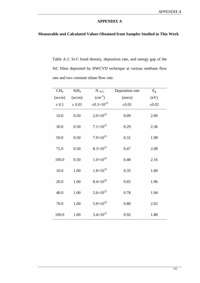
APPENDIX A
193
APPENDIX A
Measurable and Calculated Values Obtained from Samples Studied in This Work
Table A.1: Si-C bond density, deposition rate, and energy gap of the
SiC films deposited by HWCVD technique at various methane flow
rate and two constant silane flow rate.
CH4
(sccm)
± 0.1
SiH4
(sccm)
± 0.01
N Si-C
(cm-3
)
±0.1×10²³
Deposition rate
(nm/s)
±0.01
Eg
(eV)
±0.02
10.0 0.50 2.0×10²³
0.09 2.00
30.0 0.50 7.1×10²²
0.29 2.36
50.0 0.50 7.9×10²²
0.31 1.98
75.0 0.50 8.3×10²²
0.47 2.08
100.0 0.50 1.0×10²³
0.40 2.16
10.0 1.00 1.8×10²³
0.35 1.60
20.0 1.00 8.4×10²²
0.65 1.96
40.0 1.00 5.6×10²²
0.78 1.94
70.0 1.00 5.9×10²²
0.80 2.02
100.0 1.00 3.4×10²²
0.92 1.88
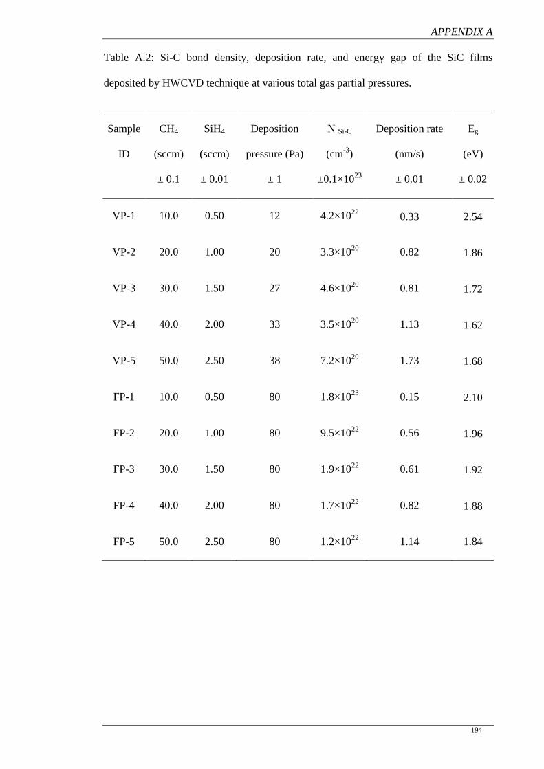
APPENDIX A
194
Table A.2: Si-C bond density, deposition rate, and energy gap of the SiC films
deposited by HWCVD technique at various total gas partial pressures.
Sample
ID
CH4
(sccm)
± 0.1
SiH4
(sccm)
± 0.01
Deposition
pressure (Pa)
± 1
N Si-C
(cm-3
)
±0.1×10²³
Deposition rate
(nm/s)
± 0.01
Eg
(eV)
± 0.02
VP-1 10.0 0.50 12 4.2×10²²
0.33 2.54
VP-2 20.0 1.00 20 3.3×10²⁰
0.82 1.86
VP-3 30.0 1.50 27 4.6×10²⁰
0.81 1.72
VP-4 40.0 2.00 33 3.5×10²⁰
1.13 1.62
VP-5 50.0 2.50 38 7.2×10²⁰
1.73 1.68
FP-1 10.0 0.50 80 1.8×10²³
0.15 2.10
FP-2 20.0 1.00 80 9.5×10²²
0.56 1.96
FP-3 30.0 1.50 80 1.9×10²²
0.61 1.92
FP-4 40.0 2.00 80 1.7×10²²
0.82 1.88
FP-5 50.0 2.50 80 1.2×10²²
1.14 1.84
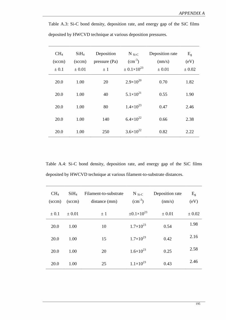
APPENDIX A
195
Table A.3: Si-C bond density, deposition rate, and energy gap of the SiC films
deposited by HWCVD technique at various deposition pressures.
CH4
(sccm)
± 0.1
SiH4
(sccm)
± 0.01
Deposition
pressure (Pa)
± 1
N Si-C
(cm-3
)
± 0.1×10²³
Deposition rate
(nm/s)
± 0.01
Eg
(eV)
± 0.02
20.0 1.00 20 2.9×10²⁰
0.70 1.82
20.0 1.00 40 5.1×10²¹
0.55 1.90
20.0 1.00 80 1.4×10²³
0.47 2.46
20.0 1.00 140 6.4×10²²
0.66 2.38
20.0 1.00 250 3.6×10²²
0.82 2.22
Table A.4: Si-C bond density, deposition rate, and energy gap of the SiC films
deposited by HWCVD technique at various filament-to-substrate distances.
CH4
(sccm)
± 0.1
SiH4
(sccm)
± 0.01
Filament-to-substrate
distance (mm)
± 1
N Si-C
(cm-3
)
±0.1×10²³
Deposition rate
(nm/s)
± 0.01
Eg
(eV)
± 0.02
20.0 1.00 10 1.7×10²³
0.54 1.98
20.0 1.00 15 1.7×10²³
0.42 2.16
20.0 1.00 20 1.6×10²³
0.25 2.58
20.0 1.00 25 1.1×10²³
0.43 2.46