high-speed pcb trace design using a behavioral surface
TRANSCRIPT

Scholars' Mine Scholars' Mine
Masters Theses Student Theses and Dissertations
Spring 2019
High-speed PCB trace design using a behavioral surface High-speed PCB trace design using a behavioral surface
roughness model and high-speed test coupon design with non-roughness model and high-speed test coupon design with non-
functional pads functional pads
Han Gao
Follow this and additional works at: https://scholarsmine.mst.edu/masters_theses
Part of the Electrical and Computer Engineering Commons
Department: Department:
Recommended Citation Recommended Citation Gao, Han, "High-speed PCB trace design using a behavioral surface roughness model and high-speed test coupon design with non-functional pads" (2019). Masters Theses. 7884. https://scholarsmine.mst.edu/masters_theses/7884
This thesis is brought to you by Scholars' Mine, a service of the Missouri S&T Library and Learning Resources. This work is protected by U. S. Copyright Law. Unauthorized use including reproduction for redistribution requires the permission of the copyright holder. For more information, please contact [email protected].

HIGH-SPEED PCB TRACE DESIGN USING A BEHAVIORAL SURFACE
ROUGHNESS MODEL AND HIGH-SPEED TEST COUPON DESIGN WITH NON-
FUNCTIONAL PADS
by
HAN GAO
A THESIS
Presented to the Faculty of the Graduate School of the
MISSOURI UNIVERSITY OF SCIENCE AND TECHNOLOGY
In Partial Fulfillment of the Requirements for the Degree
MASTER OF SCIENCE IN ELECTRICAL ENGINEERING
2019
Approved by:
Dr. James L. Drewniak, Advisor
Dr. Victor Khilkevich, Co-Advisor
Dr. Jun Fan

2019
Han Gao
All Rights Reserved

iii
ABSTRACT
In high-speed digital systems as data rates increase to tens of gigabits per second,
the loss from the conductor surface roughness cannot be ignored. Djordjeic and Huray
roughness model is widely used to count for the conductor roughness loss. However the
practical application of the existed models are not straight forward since the frequency-
dependent dielectric loss is usually unknown, leading to high discrepancies at high
frequencies (above 10 GHz). To solve this problem, a behavioral model was developed
by adding a dispersive term to the dielectric. The dispersive term in the model captures
dispersion behavior observed in the measurement accurately. The proposed model is
validated by measurement on both single-ended and differential transmission lines. Based
on behavioral model, another physic dielectric model with dispersive term added to bulk
dielectric used together with the Huray surface roughness model to represent the loss due
to roughness on traces.
Based on the theory proposed above, a new method to extract Dielectric constant
(Dk) and dissipation factor (Df) is developed. According this new method sensitivity
study, when transmission lines are tighter coupled, the more accurate of the extracted
results. However, most of the industries test coupon are built with loss coupling.
Therefore, a strong coupling test coupon with working frequency up to 50GHz need to
build to verify this new extraction method. During optimization of footprint, non-
functional pads are applied to reduce high impedance caused by current loops, especially
for the last several bottom layers.

iv
ACKNOWLEDGMENTS
I would like to sincerely express my gratitude to Dr. James Drewniak, my adviser,
for teaching me to be rigorous and responsible, for and teaching me great skills in doing
research. I am thankful for his warm encouragement when I was facing difficulties in
projects and life. He provided great support to my study during the master’s degree and
enlightened my way to the future.
I would like to thank Dr. Victor Khilkevich, my co-adviser, for his patient, kind
instructions and directions for this thesis, especially for walking me through the
beginning.
I would like to thank Dr. Jun Fan for his teaching in my courses, helpful
suggestions on my studies, and providing great inspiration to my academic and career
path. He gave me a lot of support during my study.
I would like to express my thanks to all other faculty members and students in the
EMC lab for their help. It has been a great pleasure to be a member of the lab.

v
TABLE OF CONTENTS
Page
ABSTRACT ....................................................................................................................... iii
ACKNOWLEDGMENTS ................................................................................................. iv
LIST OF ILLUSTRATIONS ............................................................................................ vii
LIST OF TABLES ...............................................................................................................x
SECTION
1. INTRODUCTION ...................................................................................................... 1
2. BACKGROUD STUDY ............................................................................................ 4
2.1. POSSIBLE PHYSICS OF ANOMALOUS OF |S21| BEHAVIORAL .............. 4
2.2. ROUGHNESS CALCULATION BASED ON CROSS-SECTION ................ 12
2.3. DISPERSIVE BEHAVIOR IN REAL MATERIALS ..................................... 13
3. BEHAVIORAL MODEL ......................................................................................... 15
3.1. MODEL DESCRIPTION ................................................................................. 15
3.2. MODEL PARAMETERS EXTRACTION ...................................................... 19
3.3. DIFFERENTIAL TRANSMISSION LINE PARAMETERS
CALCULATION.............................................................................................. 23
3.3.1. Even And Odd Mode P.U.L RLGC Calculation .................................... 23
3.3.2. Converting Even And Odd Mode Parameters To Mixed Mode ............. 25
3.4. MODEL VALIDATION .................................................................................. 26
3.4.1. Single-Ended Model Validation ............................................................. 27
3.4.2. Differential Model Validation ................................................................ 29
4. PHYSIC BASED DIELECTRIC MODEL WITH HURAY MODEL .................... 33

vi
4.1. MODEL DESCRIPTION ................................................................................. 33
4.2. MODEL PARAMETERS EXTRACTION ...................................................... 34
4.3. CURVE FITTING FOR SURFACE ROUGHNESS ....................................... 36
4.4. MODEL VALIDATION AND COMPARISON WITH
BEHAVIORAL MODEL (SINGLE-ENDED MODEL) ................................. 37
5. HIGH SPEAD TIGHT COUPLING TEST COUPON WITH NON-
FUNCTIONAL DESIGN ......................................................................................... 41
5.1. DESIGN SPACE INVESTIGATION .............................................................. 41
5.2. PROPOSED STACKUP ................................................................................... 43
5.3. VIA OPTIMIZATION ...................................................................................... 45
5.3.1. 95ohm Via Optimization ........................................................................ 45
5.3.2. 100ohm Via Optimization ...................................................................... 51
5.4. PCB LAYOUT ................................................................................................. 55
BIBLIOGRAPHY ..............................................................................................................57
VITA ..................................................................................................................................60

vii
LIST OF ILLUSTRATIONS
Figure Page
1.1. Comparison between Measurement |S21| and Hemisphere model |S21| in dB. ............. 1
1.2. Surface roughness correction factor comparison among Hammerstad
model, Hemisphere model and Huray model. .............................................................. 2
2.1. Incident wave and scattered wave on a sphere. ........................................................... 4
2.2. Total radiation power and measured insertion loss...................................................... 5
2.3. Geometries and port setting in CST simulation. .......................................................... 6
2.4. Properties of the additional dielectric layer. ................................................................ 8
2.5. Simulated S-parameters for 56mil transmission line ................................................... 9
2.6. Accepted loss with surface roughness sweeping from 0 to 25.4µm. ......................... 10
2.7. Measured insertion loss with trace width 9.5mil and 15mil with HVLP,
RTF and STD foil type .............................................................................................. 11
2.8. Equivalent roughness calculation on foil side and oxide side ................................... 12
2.9. Comparison equivalent roughness calculation among four different
surface roughness ....................................................................................................... 13
2.10. Measured Df on 10GHz, 15GHz and 21GHz and curve fitting along frequency
from 0Hz to 50GHz. ................................................................................................ 14
3.1. Total dielectric constant is contributed by non-dispersive term and dispersive term. 16
3.2. Model parameters for behavioral model. ................................................................... 16
3.3. Flow chart to calculate non-dispersive term and dispersive term. ............................. 17
3.4. Modeled non-dispersive term and dispersive term against frequency. ...................... 18
3.5. Modeled total dielectric constant and dissipation factor. ........................................... 18
3.6. Test vehicle to do parameter extraction. .................................................................... 19

viii
3.7. Parameters extraction with different foil type and different trace width
on Megtron6 test vehicles. ......................................................................................... 20
3.8. Surface fitting for model parameters. ........................................................................ 21
3.9. Cross-section view for tanδs and fitting equation. ..................................................... 22
3.10. Cross-section view for fs and fitting equation. ........................................................ 22
3.11. Port assignment for a symmetric transmission line model. ..................................... 25
3.12. Design space for behavioral model. ........................................................................ 27
3.13. Comparison among measurements, behavioral model and ADS model on
frequency domain and time domain: Megtron7 material (single-ended). ................ 28
3.14. Comparison among measurements, behavioral model and ADS model on
frequency domain and time domain: DVN material (single-ended). ....................... 28
3.15. Comparison among measurements, behavioral model and ADS model on
frequency domain and time domain: Megtron7 material (differential). .................. 30
3.16. Comparison among measurements, behavioral model and ADS model on
frequency domain and time domain: DVN material (differential). ......................... 31
4.1. Proposed physic based dielectric model with Huray model. ..................................... 33
4.2. Huray model explanation. .......................................................................................... 34
4.3. Gould snowball radii distribution of threated drum side from SEM method. ........... 34
4.4. Huray correction factor with different number of snowball against frequency. ........ 35
4.5. Model parameter extraction based on Megtron6 PCBs. ............................................ 36
4.6. Curve fitting for number of snowballs against surface roughness. ............................ 37
4.7. Comparison among measurements, behavioral model and ADS model on
frequency domain and time domain: Megtron7 material (physic based model). ...... 38
4.8. Comparison among measurements, behavioral model and ADS model on
frequency domain and time domain: DVN material (physic based model). .............. 39
5.1. Design space for strong coupling test coupon. .......................................................... 42
5.2. Error percentage for different trace width and spacing. ............................................ 43

ix
5.3. Proposed stackup. ...................................................................................................... 44
5.4. Finalized stackup by vendor. ..................................................................................... 45
5.5. HFSS model with 2.4mm SMA connectors included. ............................................... 46
5.6. 500mil space between connectors. ............................................................................. 46
5.7. Port impedance are 100ohm for 2.4mm connector side and 96ohm for trace side. ... 47
5.8. Simulated S-parameters. ............................................................................................ 48
5.9. An additional non-functional pad is added at layer5 ................................................. 49
5.10. Simulated S-parameters with non-functional pad. ................................................... 50
5.11. HFSS model for 100ohm via optimization, 2.4mm SMA connectors
model are included ................................................................................................... 51
5.12. HFSS model geometries. ......................................................................................... 52
5.13. An additional non-functional pad is added at layer3 ............................................... 53
5.14. Port impedance check: 100ohm for both connector side and trace side. ................. 53
5.15. Simulated results from HFSS................................................................................... 54
5.16. PCB layout ............................................................................................................... 55

x
LIST OF TABLES
Table Page
2.1. Surface roughness range for different foil types ........................................................ 11
2.2. Measured Dk and Df from SPDR method ................................................................. 14
3.1. Peak value from single bit response comparison: Megtron7 (single-ended) ............. 28
3.2. Peak value from single bit response comparison: DVN (single-ended) .................... 29
3.3. Peak values of single bit response comparison among validation set ....................... 29
3.4. Rms error based on measurement results comparison between behavioral model
and ADS model .......................................................................................................... 29
3.5. Peak value from single bit response comparison: Megtron7 (differential) ................ 30
3.6. Peak value from single bit response comparison: DVN (differential) ....................... 31
3.7. Single bit response peak value comparison between measurements and
behavioral model…………………………………………………………….………31
3.8. Rms error based on measurement results comparison between behavioral
model and ADS model ............................................................................................... 32
4.1. Snowball number against surface roughness ............................................................. 37
4.2. Snowball number against surface roughness (Megtron7) .......................................... 38
4.3. Snowball number against surface roughness (DVN) ................................................. 39
4.4. Single bit response peak values comparison among measurement, behavioral
model, physical based dielectric model and ADS .................................................... 39
4.5. RMS error comparison among behavioral model, physical based dielectric
model and ADS based on measurements ................................................................... 40
5.1. Calculated trace width and spacing against target impedance ................................... 42
5.2. Calculated trace width and spacing against target impedance from vendor .............. 44
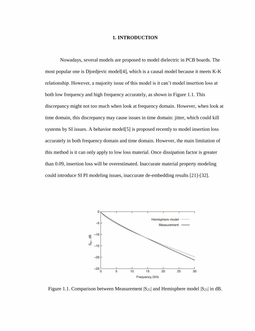
1. INTRODUCTION
Nowadays, several models are proposed to model dielectric in PCB boards. The
most popular one is Djordjevic model[4], which is a causal model because it meets K-K
relationship. However, a majority issue of this model is it can’t model insertion loss at
both low frequency and high frequency accurately, as shown in Figure 1.1. This
discrepancy might not too much when look at frequency domain. However, when look at
time domain, this discrepancy may cause issues in time domain: jitter, which could kill
systems by SI issues. A behavior model[5] is proposed recently to model insertion loss
accurately in both frequency domain and time domain. However, the main limitation of
this method is it can only apply to low loss material. Once dissipation factor is greater
than 0.09, insertion loss will be overestimated. Inaccurate material property modeling
could introduce SI PI modeling issues, inaccurate de-embedding results [21]-[32].
Figure 1.1. Comparison between Measurement |S21| and Hemisphere model |S21| in dB.

2
In addition, multiple models are proposed to model surface roughness on copper:
hammerstad model, hemispherical model and huray model. The correction factors from
three models are comparing in Figure 1.2. The major issue for hammerstad model is once
surface roughness in rms value is greater than 2um, roughness factor will be saturated
which will lead loss underestimated. Based on hammerstad model, hemispherical model
is proposed. Hemispherical correction factor is calculated by the ratio of then power
absorbed with and without a good conducting [6]. Another popular model, huray model,
is used in industry. Based on [6], hemisphere model overestimates roughness at low
frequency and underestimates at high frequency. Only huray factor provides an accurate
estimation. Therefore, huray model will be used to model surface roughness in this paper.
Figure 1.2. Surface roughness correction factor comparison among Hammerstad model,
Hemisphere model and Huray model.
In Section 2, a high-speed PCB board with strong coupling traces are designed.
During via-transition optimization, a high impedance caused by current loops between

3
signal via and GND vias cannot be removed following regular optimization flow.
Therefore, a new technique: non-functional pads are added to top layers to help reduce
this high impedance.

4
2. BACKGROUD STUDY
2.1. POSSIBLE PHYSICS OF ANOMALOUS OF |S21| BEHAVIORAL
According to Hemispherical model of roughness, as shown in Figure 2.1, power
scatted and absorbed by a sphere divided by incident flux is known as total radar cross-
section, as shown in Equation (1). The total radar cross-section of sphere is summation
over a spherical harmonics.
Figure 2.1. Incident wave and scattered wave on a sphere.
𝜎𝑡 = −𝜋
𝑘2∑ (2𝑙 + 1)𝑅𝑒[𝛼(𝑙) + 𝛽(𝑙)]𝑙 (1)
where k=2π/λ, 𝜆 =𝑐
𝑓√ ′, c is the speed of light. The scattering coefficients are
approximated assuming that kr << 1, where r is the sphere radius and are given by[2].
Therefore, based on the equation above, total radius power against with frequency can
plot as in Figure 2.2.
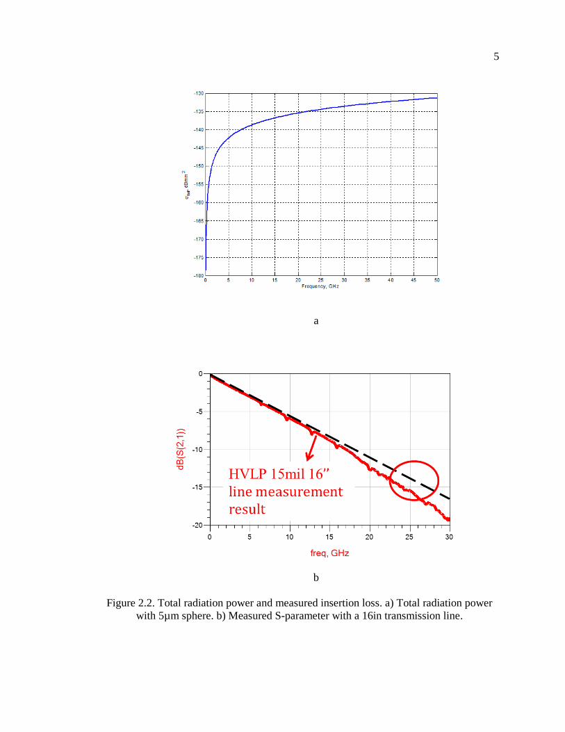
5
a
b
Figure 2.2. Total radiation power and measured insertion loss. a) Total radiation power
with 5µm sphere. b) Measured S-parameter with a 16in transmission line.
6
As shown in Figure 2.2, when frequency goes up above 10GHz, total radar cross-
section is behaved quasi-linear. Therefore, roughness couldn’t explain why we have
discrepancy between measurement and expectation (at high frequency, measured S-
parameters has frequency-depended behavior).
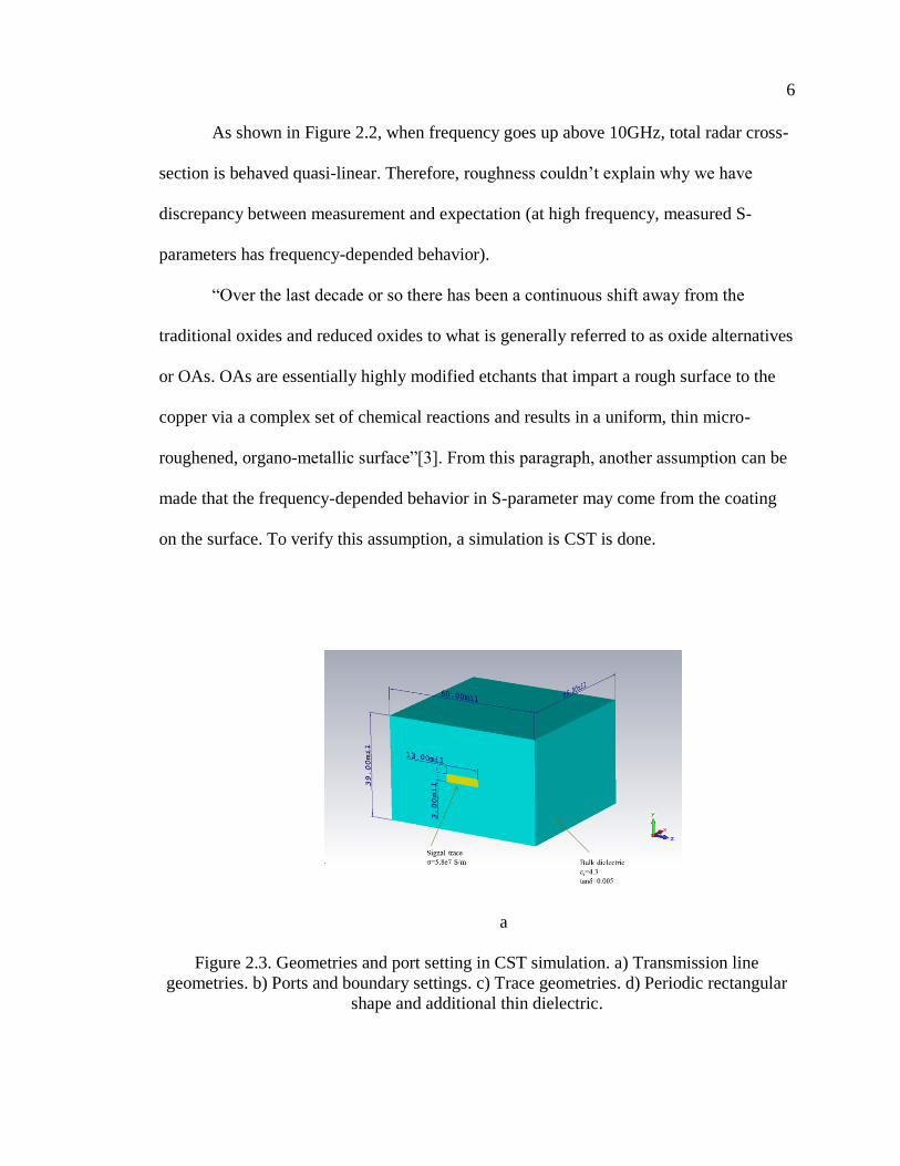
“Over the last decade or so there has been a continuous shift away from the
traditional oxides and reduced oxides to what is generally referred to as oxide alternatives
or OAs. OAs are essentially highly modified etchants that impart a rough surface to the
copper via a complex set of chemical reactions and results in a uniform, thin micro-
roughened, organo-metallic surface”[3]. From this paragraph, another assumption can be
made that the frequency-depended behavior in S-parameter may come from the coating
on the surface. To verify this assumption, a simulation is CST is done.
a
Figure 2.3. Geometries and port setting in CST simulation. a) Transmission line
geometries. b) Ports and boundary settings. c) Trace geometries. d) Periodic rectangular
shape and additional thin dielectric.

7
b
c
d
Figure 2.3. Geometries and port setting in CST simulation. a) Transmission line
geometries. b) Ports and boundary settings. c) Trace geometries. d) Periodic rectangular
shape and additional thin dielectric. (Cont.)
8
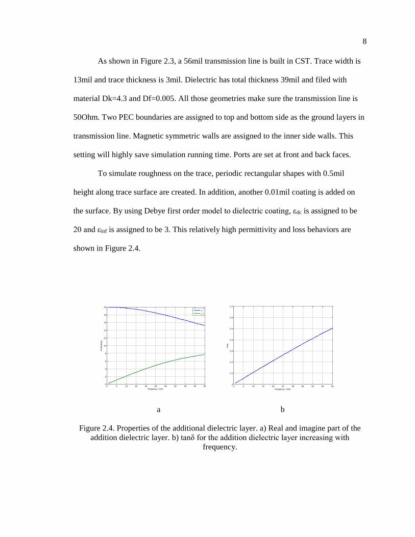
As shown in Figure 2.3, a 56mil transmission line is built in CST. Trace width is
13mil and trace thickness is 3mil. Dielectric has total thickness 39mil and filed with
material Dk=4.3 and Df=0.005. All those geometries make sure the transmission line is
50Ohm. Two PEC boundaries are assigned to top and bottom side as the ground layers in
transmission line. Magnetic symmetric walls are assigned to the inner side walls. This
setting will highly save simulation running time. Ports are set at front and back faces.
To simulate roughness on the trace, periodic rectangular shapes with 0.5mil
height along trace surface are created. In addition, another 0.01mil coating is added on
the surface. By using Debye first order model to dielectric coating, εdc is assigned to be
20 and εinf is assigned to be 3. This relatively high permittivity and loss behaviors are
shown in Figure 2.4.
a b
Figure 2.4. Properties of the additional dielectric layer. a) Real and imagine part of the
addition dielectric layer. b) tanδ for the addition dielectric layer increasing with
frequency.
0 5 10 15 20 25 30 35 40 45 500
2
4
6
8
10
12
14
16
18
20
Frequency, GHz
Perm
ittivity
'
''
0 5 10 15 20 25 30 35 40 45 500
0.1
0.2
0.3
0.4
0.5
0.6
0.7
Frequency, GHz
tan

9
From Figure 2.4, Df is increasing linearly with frequency. Therefore, what we
observed in Figure 2.2 can’t explain the loss frequency-depended behavior in S-
parameters. Thus, ω2 term should be expected in |S21| curves.
As Figure 2.5 show, loss at 50GHz is still less than -0.12dB due to extremely
short transmission line. This will lead to the return loss is comparable to the loss in the
transmission line. Therefore, accepted loss is used instead of S21.the accepted loss
equation is shown in Equation (2).
a
b
Figure 2.5. Simulated S-parameters. a) Simulated insertion loss (|S21|). b) Simulated
return loss (|S11|).

10
𝑃𝑎𝑐𝑐 = |𝑆11|2 + |𝑆21|
2 (2)
Simulations are done from total smooth case to very roughness cases. Hrms values
are used to present roughness level, which is defined as rms value of roughness peaks.
h𝑟𝑚𝑠 = √1
n∑ 𝑥𝑖
2𝑛1 (3)
where n is the number of peaks and xi is value of the ith peak. All accpeted loss are
shown in Figure 2.6. Peak values and rms values for differential foil types are list in
Table 2.1.
Figure 2.6. Accepted loss with surface roughness sweeping from 0 to 25.4µm.

11
Table 2.1. Surface roughness range for different foil types.
a b
Figure 2.7. Measured insertion loss with trace width 9.5mil and 15mil with HVLP, RTF
and STD foil type. a) 9.5mil trace width with different foil type. b) 15mil trace width
measurements with different foil types.
From Figure 2.6, when surface roughness is moderate, the frequency depended
behavior is obviously. ω2 term increases with roughness. In addition, contribution of the
ω2 term decrease and eventually the linear term dominates. Finally, when roughness

12
effect is pretty strong, there is no ω2 behavior can be observed. By comparing with
measured S-parameters on Megtron6 with trace width 9.5mil and 15mil, which are shown
in Figure 2.7, when foil type is HVLP, the frequency-depended behavior is significantly
observed and when foil type change to STD, such behavior is vanished. Therefore, we
can make the conclusion that this additional dispersive lossy layer could be a reason for
the anomalous behavior of |S21|.
2.2. ROUGHNESS CALCULATION BASED ON CROSS-SECTION
A simulation is done to investigate how does surface roughness impact insertion
loss, especially when foil side and oxide side have different surface roughness value.
Figure 2.8. Equivalent roughness calculation on foil side and oxide side.
13
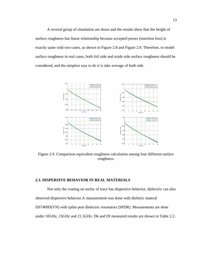
A several group of simulation are down and the results show that the height of
surface roughness has linear relationship because accepted power (insertion loss) is
exactly same with two cases, as shown in Figure 2.8 and Figure 2.9. Therefore, to model
surface roughness in real cases, both foil side and oxide side surface roughness should be
considered, and the simplest way to do it is take average of both side.
Figure 2.9. Comparison equivalent roughness calculation among four different surface
roughness.
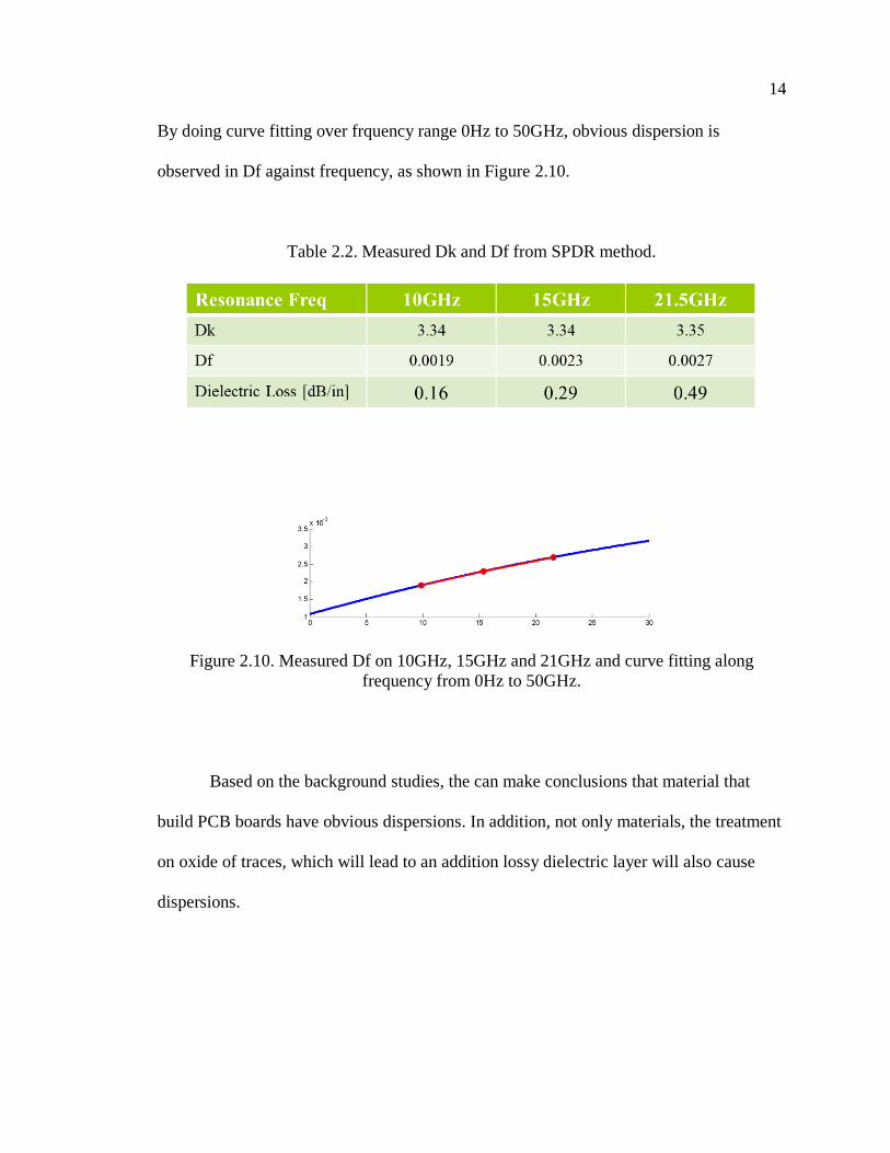
2.3. DISPERSIVE BEHAVIOR IN REAL MATERIALS
Not only the coating on surfac of trace has dispersive behavior, dielectric can also
observed dispersive behavior.A measurement was done with dieletric materal
DS7409D(VN) with splite post dielectric resonators (SPDR). Measuements are done
under 10GHz, 15GHz and 21.5GHz. Dk and Df measured results are shown in Table 2.2.
14
By doing curve fitting over frquency range 0Hz to 50GHz, obvious dispersion is
observed in Df against frequency, as shown in Figure 2.10.
Table 2.2. Measured Dk and Df from SPDR method.
Figure 2.10. Measured Df on 10GHz, 15GHz and 21GHz and curve fitting along
frequency from 0Hz to 50GHz.
Based on the background studies, the can make conclusions that material that
build PCB boards have obvious dispersions. In addition, not only materials, the treatment
on oxide of traces, which will lead to an addition lossy dielectric layer will also cause
dispersions.

15
3. BEHAVIORAL MODEL
3.1. MODEL DESCRIPTION
In an earlier study [4], a practical causal approximation for low-dispersive
dielectrics often used in the PCBs (Djordjevic model [5]) is presented. The dielectric
constant was calculated as Equation (4) and (5).
Re{휀𝑟(𝜔)} = 휀′ ≈ 휀∞′ +
∆ ′
𝑚2−𝑚1
𝑙𝑛(𝜔2𝜔)
ln(10) (4)
Im{휀𝑟(𝜔)} = 휀′′ ≈∆ ′
𝑚2−𝑚1
−𝜋
2
ln(10) (5)
Besides the dielectric parameters 휀∞′ and ∆휀′, the model is characterized by two
frequency limits 𝜔1 = 10𝜔1and𝜔2 = 10𝜔2. Usually the lower frequency limit is set to a
kHz value and the upper one is set to a THz value. This allows generating the causal
dielectric constant function that is practically constant in the frequency range of interest
of typical signal integrity simulations (MHz – tens of GHz). Most of the dielectrics used
for PCB manufacturing are indeed very low-dispersive (at least starting from 5-10 GHz)
[6 - 12]. However as was indicated above, the low-loss transmission lines, often exhibit
an increase in the slope of the insertion loss (S21) curve with frequency, which cannot be
accounted by the existing models.
Although typical PCB dielectrics have low dispersion, it is possible to model the
frequency-dependent slope of S21 by adding an effective dispersive dielectric term to the
bulk dielectric, accounting for the roughness effect in this manner.
In the proposed model, the bulk dielectric of the transmission line is calculated as
휀𝑡𝑜𝑡 = 휀1 + 휀2, as shown in Figure 3.1, where both terms 휀1 and 휀2are calculated

16
according to Djordjevic (as shown in Equations 1 and 2). The first term is non-dispersive
and describes the ‘nominal’ behavior of the dielectric and the second term is dispersive
and accounts for the roughness effect, as shown in Figure 3.1.
Figure 3.1. Total dielectric constant is contributed by non-dispersive term and dispersive
term.
The parameters of the non-dispersive term 휀1 are calculated by specifying the
desired values of 휀′ and tanδ at a certain frequency, and using the frequency limits 𝜔1and
𝜔2in the kHz and THz frequency range correspondingly.
Figure 3.2. Model parameters for behavioral model.

17
Similar procedure is applied to calculate the dispersive part 휀2with the following
exceptions: the 휀2′ is set such that 휀2
′ ≪휀1′ (in the examples below, 휀2
′ is set to 0.1 for 휀1′
≈4); the lower frequency limit 𝜔1=2πfs is set in the GHz frequency range; and tanδs is
specified at the lower frequency limit. The two parameters of the dispersive term (tanδs
and fs) are illustrated in Figure 3.2.
In summary, the procedure to calculate bulk dielectric term and dispersive term
are illustrated in Figure 3.3.
a b
Figure 3.3. Flow chart to calculate non-dispersive term and dispersive term.
Figure 3.4 shows an example for bulk dielectric 휀𝑡𝑜𝑡 plot that was calculated using
this method. The non-dispersive term had nominal values of DK and DF of 3.8 and 0.006
respectively. The lower frequency limit for the non-dispersive term is 10 kHz and the

18
upper one is 1 THz. For the dispersive term tanδs =0.12 and fs=9 GHz. As shown in
Figure 3.5, the proposed method allows generating the causal permittivity function that
has almost frequency independent real part (Dk) and at the same time frequency
dependent loss tangent (tanδ), the parameters of which can be set independently of Dk.
Figure 3.4. Modeled non-dispersive term and dispersive term against frequency.
Figure 3.5. Modeled total dielectric constant and dissipation factor.

19
After the permittivity function is generated, the transmission coefficient of the
stripline is calculated analytically based on an earlier study [13 - 14].
3.2. MODEL PARAMETERS EXTRACTION
The proposed model requires two parameters: fs and tanδs, both of which depend
on the roughness and the geometry of the stripline. These parameters are determined
empirically. For this study, a set of test vehicles (TV) were created, an example is shown
in Figure 3.6. The set consisted of twelve boards, each having 50 ohm single-ended 16
inch striplines of three different roughness grades (STD, RTF/VLP, and HVLP) and four
different widths (3.5, 9.5, 13 and 15 mils). All the boards contained a TRL pattern for
de-embedding purposes and were manufactured using the same dielectric material
(Megtron 6). An example of the test vehicle is demonstrated in Figure 3.6. For each TV, a
model was built as described above, using known values for the bulk dielectric
permittivity (휀1′=3.8) and loss tangent (tanδs =0.006).
The parameters of the dispersive layer fs and tanδs were tuned for each case to
ensure the best match between the measured and calculated transmission coefficients.
The transmission coefficient curves along with the tuned parameters are shown in Figure
3.7.
Figure 3.6. Test vehicle to do parameter extraction.

20
Figure 3.7. Parameters extraction with different foil type and different trace width on
Megtron6 test vehicles.
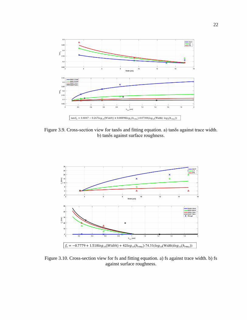
The extracted parameters of the dispersive term are shown in Figure 3.7, along
with the polynomial fitted approximation (design curves), which are illustrated in Figure
3.8, Figure 3.9 and Figure 3.10. The obtained design curves allow determining the
dispersive term parameters for arbitrary line width, provided that the roughness of the
modelled transmission-line resembles one of the roughness grades (STD, RTF/VLP,
HVLP) used for the parameter extraction.
The design curves were extracted for the Megtron6 dielectric material. However
these can be extended to be used for other low-loss materials, using the normalization
schematic as shown in Equation (6).

21
tan𝛿𝑠_𝑜𝑡ℎ𝑒𝑟 =tan𝛿0_𝑜𝑡ℎ𝑒𝑟
tan𝛿0_𝑚𝑒𝑔6tan𝛿𝑠_𝑚𝑒𝑔6 (6)
where 𝑡𝑎𝑛𝑑0_𝑚𝑒𝑔6 is the value from design curve for Megtron6 board, 𝑡𝑎𝑛𝑑0_𝑜𝑡ℎ𝑒𝑟 is the
other material dispersive term dielectric loss, 𝑡𝑎𝑛𝑑0_𝑚𝑒𝑔6 is the loss tangent for the
Megtron6 and 𝑡𝑎𝑛𝑑0_𝑜𝑡ℎ𝑒𝑟 is the loss tangent for the other material.
a
b
Figure 3.8. Surface fitting for model parameters. a) Surface fitting for tanδs. b) Surface
fitting for fs.
22
Figure 3.9. Cross-section view for tanδs and fitting equation. a) tanδs against trace width.
b) tanδs against surface roughness.
Figure 3.10. Cross-section view for fs and fitting equation. a) fs against trace width. b) fs
against surface roughness.

23
3.3. DIFFERENTIAL TRANSMISSION LINE PARAMETERS CALCULATION
To calculate S-parameters, a general way to do is calculating p.u.l RLGC term
then propagation constant can be obtained.
3.3.1. Even And Odd Mode P.U.L RLGC Calculation. According to Equation
(7) and (8) [15], even mode and odd mode impedance can be calculated separately.
𝐸𝑣𝑒𝑛 𝑚𝑜𝑑𝑒: 𝑍0𝑒(𝑤
𝑏,𝑡
𝑏,𝑠
𝑏) = {
1
𝑍0(𝑤
𝑏,𝑡
𝑏)−
𝐶𝑓′(𝑡
𝑏)
𝐶𝑓′(0)[𝑍0 (
𝑤
𝑏, 0) −
1
𝑍0𝑒(𝑤
𝑏,0,
𝑡
𝑏)]}−1 (7)
𝑂𝑑𝑑 𝑚𝑜𝑑𝑒: 𝑍0𝑜(𝑤
𝑏,𝑡
𝑏,𝑠
𝑏) = {
1
𝑍0(𝑤
𝑏,0,
𝑡
𝑏)+ [
1
𝑍0(𝑤
𝑏,𝑡
𝑏)−
1
𝑍0(𝑤
𝑏,0)] −
2
377[𝐶𝑓′(
𝑡
𝑏)−
𝐶𝑓′(0)] +2𝑡
377𝑠}−1
(8)
Considering about fringing field, p.u.l capacitance for even mode and odd mode
can be calculated as [15].
𝐸𝑣𝑒𝑛 𝑚𝑜𝑑𝑒: 𝐶𝑓′ (𝑡
𝑏) =
𝜋[2
1−𝑡
𝑏
𝑙𝑛 (1
1−𝑡
𝑏
+ 1) − (1
1−𝑡
𝑏
− 1) ln(1
(1−𝑡
𝑏)2 − 1)] (9)
𝑂𝑑𝑑 𝑚𝑜𝑑𝑒: 𝐶𝑓′ (𝑡
𝑏) =
𝜋[2
1−𝑡
𝑏
𝑙𝑛 (1
1−𝑡
𝑏
+ 1) − (1
1−𝑡
𝑏
− 1) 𝑙𝑛(1
(1−𝑡
𝑏)2 − 1)] (10)
Therefore, based on impedance calculated related to geometries with fringing
field considered, we can calculate p.u.l inductance (L), capacitance (C) and conductance
(G) by [1].
𝐶 =1
𝑣𝑍0 (11)
𝐿 = 𝐶𝑍02 (12)
𝐺 = 𝐶𝜔 tan 𝛿 (13)

24
The last transmission line parameter left is per unit length resistance (p.u.l R).
According to single-ended model parameter calculation, we can calculate resistance on
trance and ground separately by [1]:
𝑅𝑡𝑟𝑎𝑐𝑒 =1
2𝑤√𝜋𝜇𝑓
𝜎 (14)
𝑅𝑔𝑟𝑜𝑢𝑛𝑑 =1
6ℎ√𝜋𝜇𝑓
𝜎 (15)
For differential transmission line, we also need to consider proximity effect.
According to Equation (15), proximity effect correction factor for odd mode can be
calculated as [16]:
𝑝𝑟𝑜𝑥𝑖𝑚𝑖𝑡𝑦𝑐𝑜𝑟𝑟𝑒𝑐𝑡𝑖𝑜𝑛𝑓𝑎𝑐𝑡𝑜𝑟 =1
√1−(𝑤
𝑠+𝑤)2
(16)
Therefore, to calculate p.u.l resistance, we can follow Equation (17) and (18).
𝐸𝑣𝑒𝑛 𝑚𝑜𝑑𝑒: 𝑅𝑒𝑣𝑒𝑛 =1
6√𝜋𝜇𝑓
𝜎(3
𝑤+
1
ℎ) (17)
Odd mode: 𝑅𝑜𝑑𝑑 =1
6√𝜋𝜇𝑓
𝜎(3
𝑤+
1
ℎ) × 𝑝𝑟𝑜𝑥𝑖𝑚𝑖𝑡𝑦 𝑒𝑓𝑓𝑒𝑐𝑡 𝑐𝑜𝑟𝑟𝑒𝑐𝑡𝑖𝑜𝑛 𝑓𝑎𝑐𝑡𝑜𝑟
(18)
Till now, we have already got all per unit length parameters. Therefore, we can
calculate propagation constant for even mode and odd mode by Equation (19)[1].
𝛾 = √(𝑅 + 𝑗𝜔𝐿)(𝐺 + 𝑗𝜔𝐶) (19)
In addition, transmission coefficient for even and odd mode can be calculated
separately as Equation (20) [1].
𝑇 = 𝑒−𝛾𝑙 (20)
25
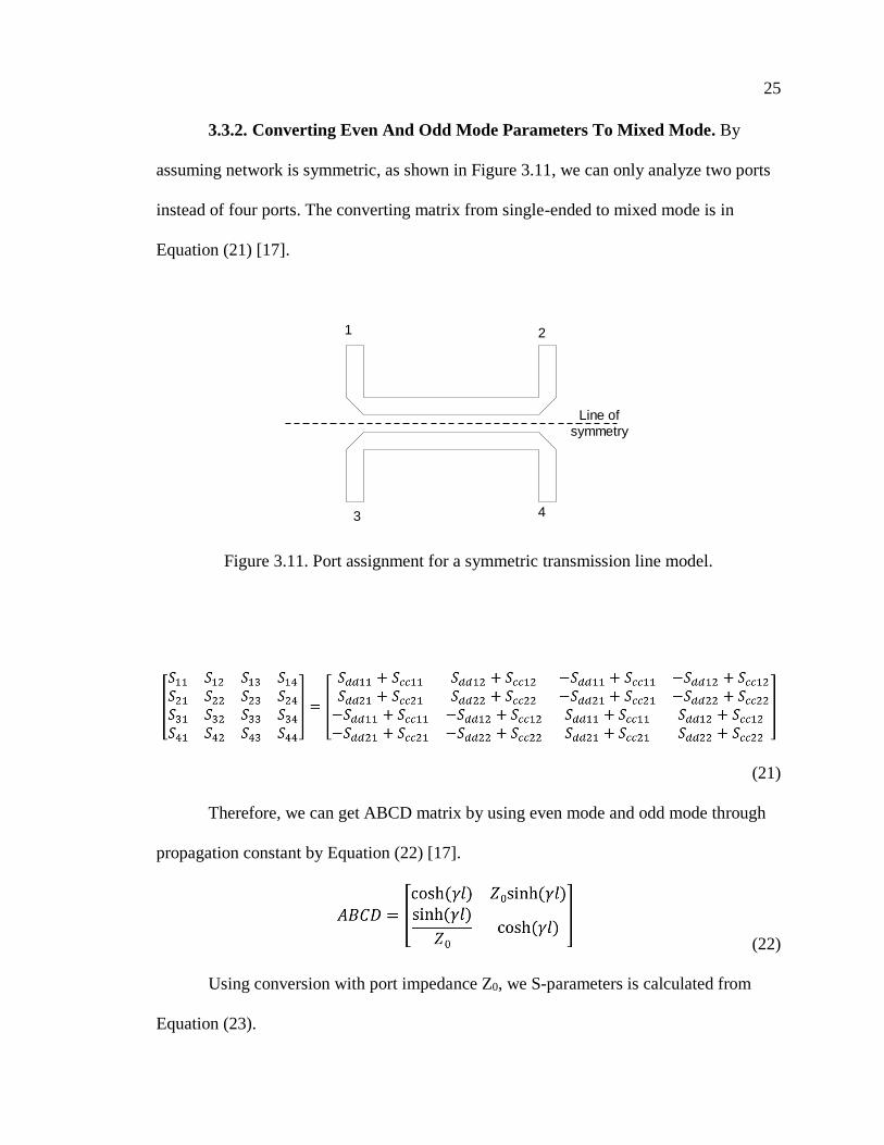
3.3.2. Converting Even And Odd Mode Parameters To Mixed Mode. By
assuming network is symmetric, as shown in Figure 3.11, we can only analyze two ports
instead of four ports. The converting matrix from single-ended to mixed mode is in
Equation (21) [17].
Line of
symmetry
1 2
43
Figure 3.11. Port assignment for a symmetric transmission line model.
(21)
Therefore, we can get ABCD matrix by using even mode and odd mode through
propagation constant by Equation (22) [17].
(22)
Using conversion with port impedance Z0, we S-parameters is calculated from
Equation (23).

26
(23)
After inputting odd mode ABCD matrix in to conversion matrix, we could get
differential mode and common S-parameters as Equation (24) and Equation (25) [17].
[𝑆𝑑𝑑11 𝑆𝑑𝑑12𝑆𝑑𝑑21 𝑆𝑑𝑑22
] =
1
2𝑍0 cosh(𝛾𝑜𝑑𝑑𝑙)+𝑍𝑜𝑑𝑑2 +𝑍0
2
𝑍𝑜𝑑𝑑sinh(𝛾𝑜𝑑𝑑𝑙)
[
𝑍𝑜𝑑𝑑2 −𝑍0
2
𝑍𝑜𝑑𝑑sinh(𝛾𝑜𝑑𝑑𝑙) 2𝑍𝑜𝑑𝑑
2𝑍𝑜𝑑𝑑𝑍𝑜𝑑𝑑2 −𝑍0
2
𝑍𝑜𝑑𝑑sinh(𝛾𝑜𝑑𝑑𝑙)
] (24)
[𝑆𝑐𝑐11 𝑆𝑐𝑐12𝑆𝑐𝑐21 𝑆𝑐𝑐22
] =
1
2𝑍0 cosh(𝛾𝑒𝑣𝑒𝑛𝑙)+𝑍𝑒𝑣𝑒𝑛2 +𝑍0
2
𝑍𝑒𝑣𝑒𝑛sinh(𝛾𝑒𝑣𝑒𝑛𝑙)
[
𝑍𝑒𝑣𝑒𝑛2 −𝑍0
2
𝑍𝑒𝑣𝑒𝑛sinh(𝛾𝑒𝑣𝑒𝑛𝑙) 2𝑍𝑒𝑣𝑒𝑛
2𝑍𝑒𝑣𝑒𝑛𝑍𝑒𝑣𝑒𝑛2 −𝑍0
2
𝑍𝑒𝑣𝑒𝑛sinh(𝛾𝑒𝑣𝑒𝑛𝑙)
] (25)
3.4. MODEL VALIDATION
For this study, twenty one cases were used to validate the behavioral model. As
shown in Figure 3.12, the validation set includes high-loss and middle-loss materials
(tanδ>0.01) as well as low-loss material (tanδ≤0.008), with different trace widths and
roughness. All validation set can be separated into two parts: when tanδ is smaller than
0.009, behavioral model has better performance, which means surface roughness need to
considered when predict S21; when tanδ is greater than 0.009, behavioral model is not
needed. Otherwise, S21 will be overestimated when comparing with measurement results,
no matter for frequency domain or time domain.

27
Figure 3.12. Design space for behavioral model.
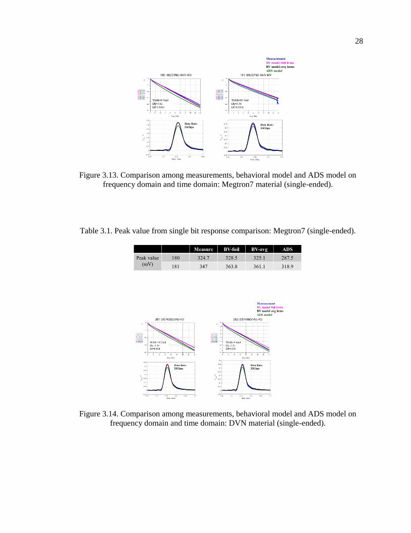
3.4.1. Single-Ended Model Validation. Figure 3.13 and Figure 3.14 shows four
examples of the validation of the behavioral model compared with the results obtained in
ADS. Each example has different trace width, material and roughness. Peak values in
millivolt from single-bit response comparing with measurements are also list in Table 3.1
and Table 3.2. Table 3.3 list all peaks values from single-bit response for validated
materials and Table 3.4 compare rms error between behavioral model, ADS model and
measurements. As we can see, behavioral model with surface roughness on both sides
considered have better results than behavioral model with foil side surface roughness
considered and ADS models. From rms error in percentage, we can see that behavioral
model with average roughness has error 2.7% only when comparing with measurements.
28
Figure 3.13. Comparison among measurements, behavioral model and ADS model on
frequency domain and time domain: Megtron7 material (single-ended).
Table 3.1. Peak value from single bit response comparison: Megtron7 (single-ended).
Figure 3.14. Comparison among measurements, behavioral model and ADS model on
frequency domain and time domain: DVN material (single-ended).

29
Table 3.2. Peak value from single bit response comparison: DVN (single-ended).
Table 3.3. Peak values of single bit response comparison among validation set.
Table 3.4. Rms error based on measurement results comparison between behavioral
model and ADS model.
3.4.2. Differential Model Validation. Figure 3.15 and Figure 3.16 shows four
examples of the validation of the behavioral model compared with the results obtained in

30
ADS. Each example has different trace width, material and roughness. Table 3.5 and
Table 3.6 list peak values of single-bit response for Megtron7 and DVN. Differential
mode peak values and common mode peak values are list separately. As we can see,
behavioral model with foil side and oxide surface roughness considered in model has
better results than model only have foil side roughness included only. Therefore, the
results prove again that surface roughness from both side of traces should be considered,
which is constant with the conclusion in background study.
Figure 3.15. Comparison among measurements, behavioral model and ADS model on
frequency domain and time domain: Megtron7 material (differential).
Table 3.5. Peak value from single bit response comparison: Megtron7 (differential).

31
Figure 3.16. Comparison among measurements, behavioral model and ADS model on
frequency domain and time domain: DVN material (differential).
Table 3.6. Peak value from single bit response comparison: DVN (differential).
A single bit response pick values summary about all validated cases for
differential pairs are list in Table 3.7.
Table 3.7. Single bit response peak value comparison between measurements and
behavioral model.

32
Finally, rms error in percentage is calculated based measurements for behavioral
model and ADS model, which is illustrated in Table 3.8. As we can see, behavioral
model with average roughness value from foil side and oxide side has error 9.25% when
comparing with measurements. However, behavioral model with surface roughness from
foil side only have error 17.3% and ADS model has rms error 19.36%. Both of these two
model have almost double error than behavioral model with surface roughness considered
from both side. Therefore, the conclusion is that the behavioral model can capture
material and surface roughness dispersion more accurate, no matter for single-ended
transmission line or differential transmission line
Table 3.8. Rms error based on measurement results comparison between behavioral
model and ADS model.
33
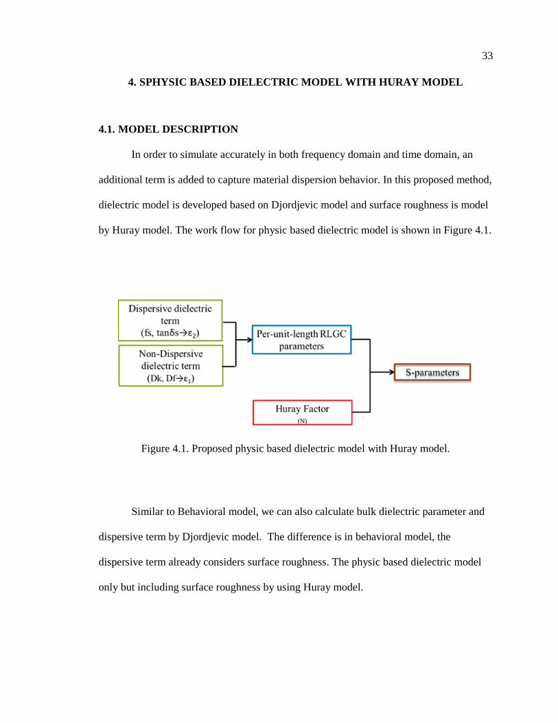
4. SPHYSIC BASED DIELECTRIC MODEL WITH HURAY MODEL
4.1. MODEL DESCRIPTION
In order to simulate accurately in both frequency domain and time domain, an
additional term is added to capture material dispersion behavior. In this proposed method,
dielectric model is developed based on Djordjevic model and surface roughness is model
by Huray model. The work flow for physic based dielectric model is shown in Figure 4.1.
Figure 4.1. Proposed physic based dielectric model with Huray model.
Similar to Behavioral model, we can also calculate bulk dielectric parameter and
dispersive term by Djordjevic model. The difference is in behavioral model, the
dispersive term already considers surface roughness. The physic based dielectric model
only but including surface roughness by using Huray model.
34
4.2. MODEL PARAMETERS EXTRACTION
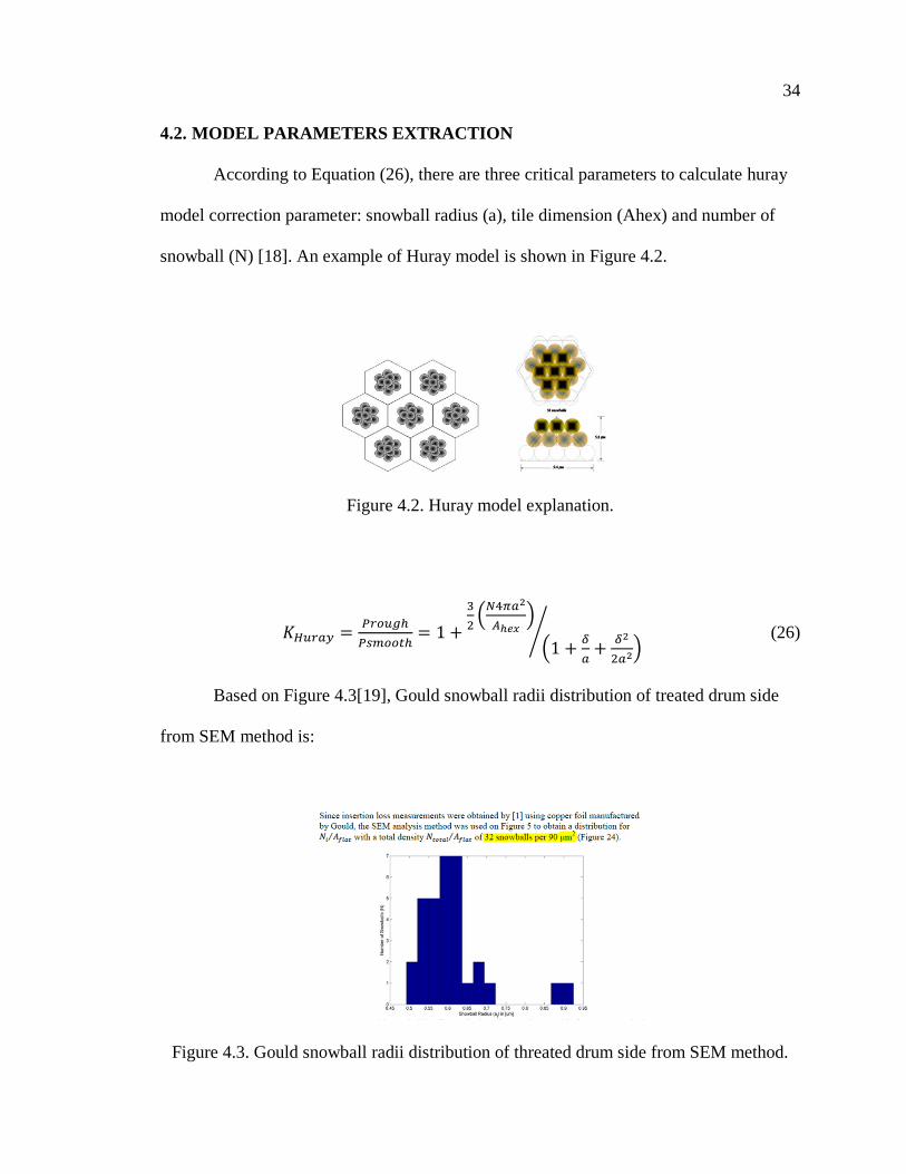
According to Equation (26), there are three critical parameters to calculate huray
model correction parameter: snowball radius (a), tile dimension (Ahex) and number of
snowball (N) [18]. An example of Huray model is shown in Figure 4.2.
Figure 4.2. Huray model explanation.
𝐾𝐻𝑢𝑟𝑎𝑦 =𝑃𝑟𝑜𝑢𝑔ℎ
𝑃𝑠𝑚𝑜𝑜𝑡ℎ= 1 +
3
2(𝑁4𝜋𝑎2
𝐴ℎ𝑒𝑥)
(1 +𝛿
𝑎+
𝛿2
2𝑎2)
⁄ (26)
Based on Figure 4.3[19], Gould snowball radii distribution of treated drum side
from SEM method is:
Figure 4.3. Gould snowball radii distribution of threated drum side from SEM method.

35
Therefore, we can fix snowball radius with a=0.63µm and tile dimension and tile
dimension Ahex=90µm2 to simplify parameter calculation. Till now, Huray model
correction factor only depends on snowball number and frequency. Figure 4.4 shows an
example that how does Huray correction factors with different snowball number change
with frequency:
Figure 4.4. Huray correction factor with different number of snowball against frequency.
To use Huray correction factor, we can just simply multiply it with p.u.l resistance
based on Equation (27).
(27)
In this new dielectric model, the assumption is same material has same dispersion
behavior. Therefore, in extraction set, fs and tanδs should be exactly same. Another
assumption is same foil type should have same number of snowball. Therefore, twelve

36
Meg6 boards, which have 3.5mil, 9.5mil, 13mil and 15mil trace width and different foil
type HVLP, VLP/RTF and STD, have same fs and tands and 3 different N numbers. The
correlation between tuned model parameters and measurement is shown in Figure 4.5.
When model other materials, a normalization is needed to do based on bulk Df, which is
also called Df1 in the model.
Figure 4.5. Model parameter extraction based on Megtron6 PCBs.
4.3. CURVE FITTING FOR SURFACE ROUGHNESS
As we know, surface roughness can vary from boards to boards due to different
foil type. Even with same foil type, surface roughness can be different due to different
manufactures. Therefore, to solve this issue, curve fitting is done based on extraction set
and equation is: N=12.95rms2+13.75rms+3.95. The curve fitting based on extraction set

37
is shown in Figure 4.6. The corresponded roughness number and number of snowball are
list in Table 4.1.
Table 4.1. Snowball number against surface roughness.
Figure 4.6. Curve fitting for number of snowballs against surface roughness.
Therefore, once surface roughness, which represent by rms value is fixed, is
known, number of snowball is known from the fitted curve.
4.4. MODEL VALIDATION AND COMPARISON WITH BEHAVIORAL MODEL
(SINGLE-ENDED MODEL)
The comparison among measurements, physic based Huray model and ADS
model are done. Two examples are shown based on Megron7 and Doosan-DVN materials
in Figure 4.7 and Figure 4.8.

38
Figure 4.7. Comparison among measurements, behavioral model and ADS model on
frequency domain and time domain: Megtron7 material (physic based model).
Table 4.2. Snowball number against surface roughness (Megtron7).
Table 4.2 and Table 4.3 list peak values of single-bit response form Megtron7 and
DVN material. As we can see, Huray model with average roughness value included have
better results than other models. Table 4.4 list peak values in millivolt from all validated
materials and compared with measurements. Table 4.5 list rms error in percentage. Huray

39
model with average roughness considered has less error, only 5.98% when comparing
with measurement results.
Figure 4.8. Comparison among measurements, behavioral model and ADS model on
frequency domain and time domain: DVN material.
Table 4.3. Snowball number against surface roughness (DVN).
Table 4.4. Single bit response peak values comparison among measurement, behavioral
model, physical based dielectric model and ADS.

40
Table 4.5. RMS error comparison among behavioral model, physical based dielectric
model and ADS based on measurements.

41
5. HIGH SPEAD TIGHT COUPLING TEST COUPON WITH NON-
FUNCTIONAL DESIGN
According to paper [20], a new method is developed to extract Dk and Df with
strong coupling transmission lines. However, most of PCB boards from industries are
built with weak coupling traces. Therefore, a test coupon is design with tight coupling
traces are designed.
5.1. DESIGN SPACE INVESTIGATION
According to requirements, the test coupon should meet following criteria:
• The differential transmission lines must be strong coupling, which is defined the
ration of spacing to dielectric height is less than 1.
• Target impedances are 100ohm, 95ohm or 92ohm.
o 100ohm transmission line have trace width around 10mil
o 95ohm or 92ohm transmission line have trace width around 4mil
• Board thickness should be around 93mil
Base on the criteria above, by sweeping trace width and spacing with:
• Core thickness: 4mil
• Prepreg thickness: 4.32mil
• Trace thickness: 0.6mil
• Glasstype: 1035 with 2ply
• Resin content: 72%
• Dk: 3.15 @1GHz
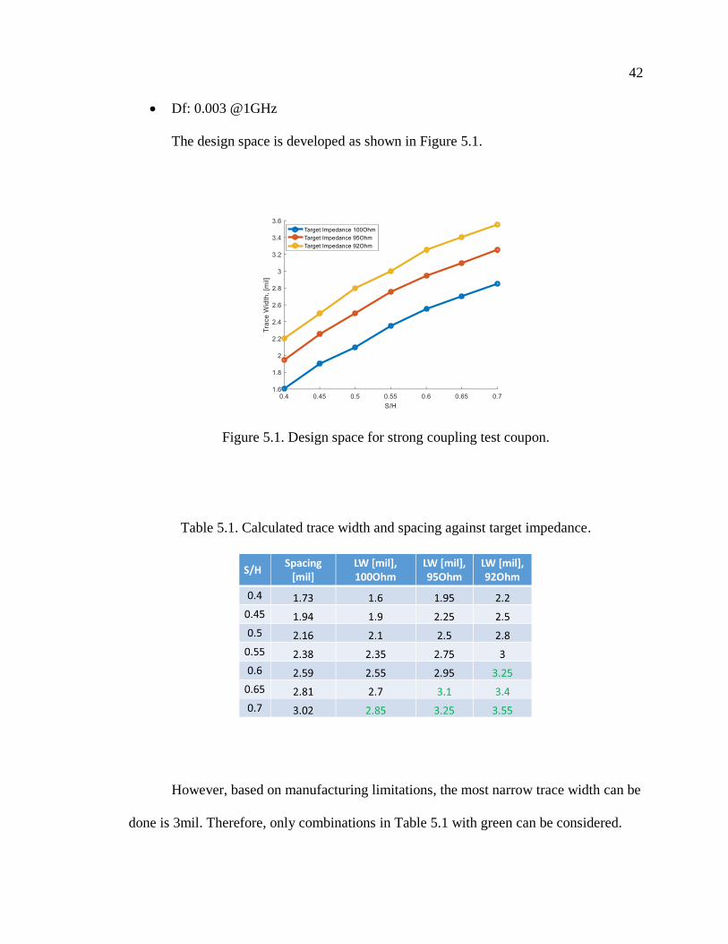
42
• Df: 0.003 @1GHz
The design space is developed as shown in Figure 5.1.
Figure 5.1. Design space for strong coupling test coupon.
Table 5.1. Calculated trace width and spacing against target impedance.
However, based on manufacturing limitations, the most narrow trace width can be
done is 3mil. Therefore, only combinations in Table 5.1 with green can be considered.
43
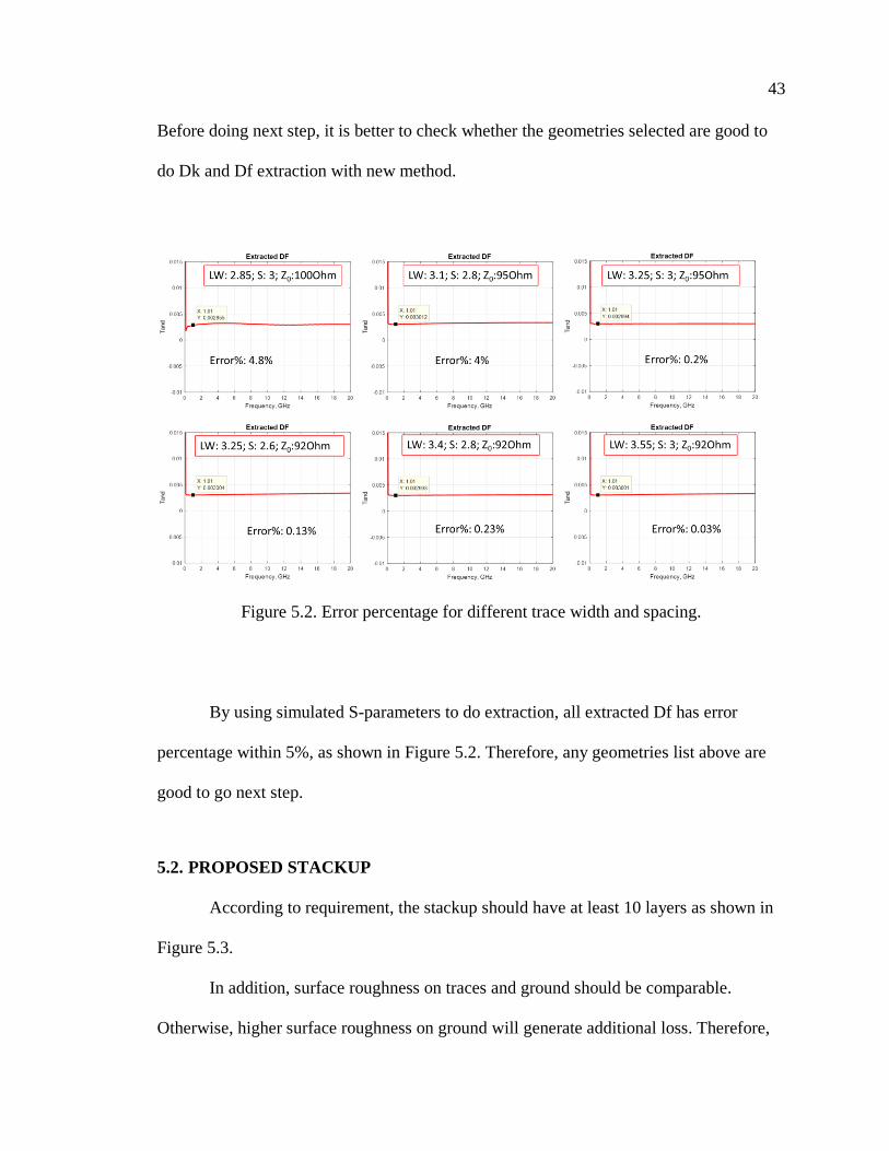
Before doing next step, it is better to check whether the geometries selected are good to
do Dk and Df extraction with new method.
Figure 5.2. Error percentage for different trace width and spacing.
By using simulated S-parameters to do extraction, all extracted Df has error
percentage within 5%, as shown in Figure 5.2. Therefore, any geometries list above are
good to go next step.
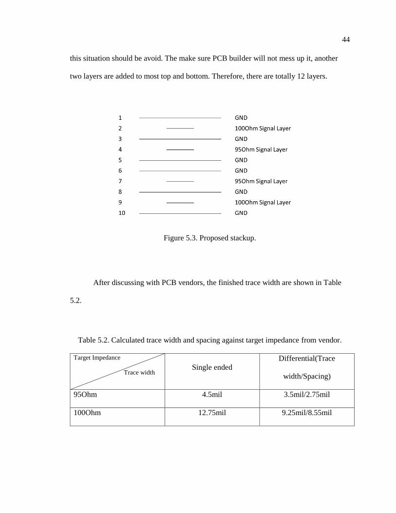
5.2. PROPOSED STACKUP
According to requirement, the stackup should have at least 10 layers as shown in
Figure 5.3.
In addition, surface roughness on traces and ground should be comparable.
Otherwise, higher surface roughness on ground will generate additional loss. Therefore,
44
this situation should be avoid. The make sure PCB builder will not mess up it, another
two layers are added to most top and bottom. Therefore, there are totally 12 layers.
Figure 5.3. Proposed stackup.
After discussing with PCB vendors, the finished trace width are shown in Table
5.2.
Table 5.2. Calculated trace width and spacing against target impedance from vendor.
Target Impedance
Trace width Single ended
Differential(Trace
width/Spacing)
95Ohm 4.5mil 3.5mil/2.75mil
100Ohm 12.75mil 9.25mil/8.55mil
45
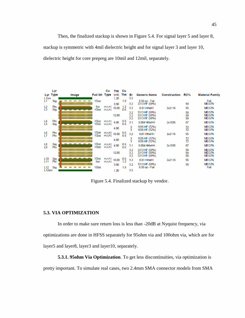
Then, the finalized stackup is shown in Figure 5.4. For signal layer 5 and layer 8,
stackup is symmetric with 4mil dielectric height and for signal layer 3 and layer 10,
dielectric height for core prepreg are 10mil and 12mil, separately.
Figure 5.4. Finalized stackup by vendor.
5.3. VIA OPTIMIZATION
In order to make sure return loss is less than -20dB at Nyquist frequency, via
optimizations are done in HFSS separately for 95ohm via and 100ohm via, which are for
layer5 and layer8, layer3 and layer10, separately.
5.3.1. 95ohm Via Optimization. To get less discontinuities, via optimization is
pretty important. To simulate real cases, two 2.4mm SMA connector models from SMA
46
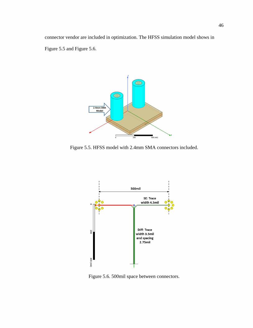
connector vendor are included in optimization. The HFSS simulation model shows in
Figure 5.5 and Figure 5.6.
Figure 5.5. HFSS model with 2.4mm SMA connectors included.
Figure 5.6. 500mil space between connectors.

47
Each signal via has 7 ground vias around. The distance between signal via and
each related ground via is 30mil to minimize inductance caused by loop from signal via
to ground vias. Both signal vias and ground vias have drill hold size 7.9mil and pad size
(inner and outer) 17mil. Dielectric constant and dissipation factor are 3.1 and 0.0025,
separately. When doing simulation, Djordjevic-Sarkar model also applied to make sure
simulation results are closed to real measurement. First, port impedance is checked before
full-wave simulation is run, which is shown in Figure 5.7.
Figure 5.7. Port impedance are 100ohm for 2.4mm connector side and 96ohm for trace
side.
Diff1 is assigned to 2.4mm SMA connectors side and Diff2 is assigned to trace
side. Diff1 has port impedance 100ohm and diff2 has port impedance 96ohm. Both port
impedance are closed to target impedance and error is within tolerance percentage.
Therefore, full-wave simulations and optimization will be done next.
48
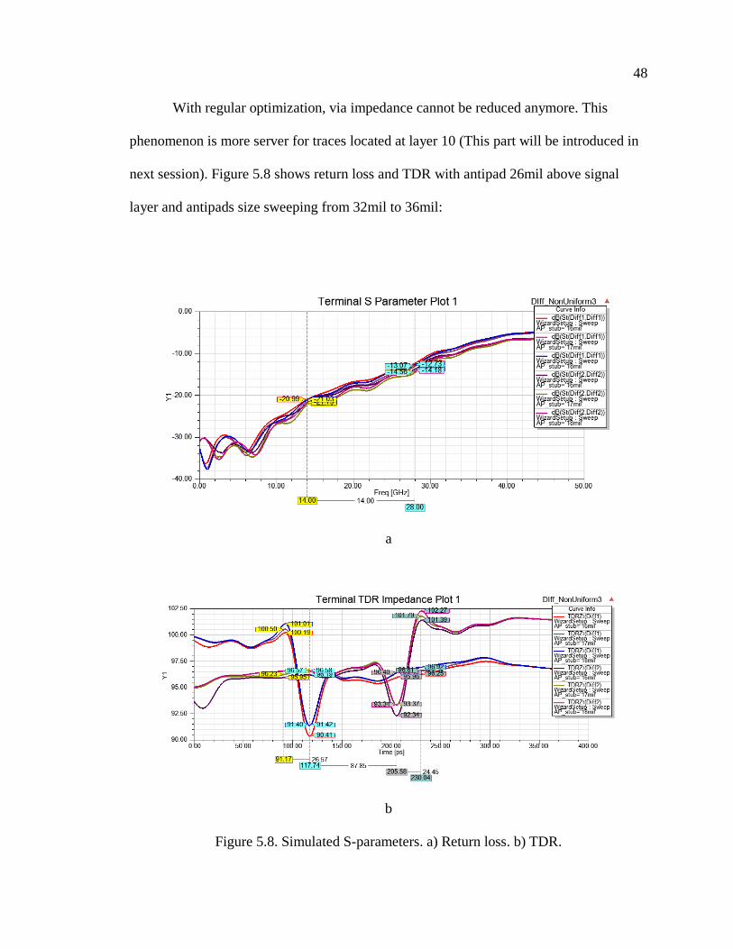
With regular optimization, via impedance cannot be reduced anymore. This
phenomenon is more server for traces located at layer 10 (This part will be introduced in
next session). Figure 5.8 shows return loss and TDR with antipad 26mil above signal
layer and antipads size sweeping from 32mil to 36mil:
a
b
Figure 5.8. Simulated S-parameters. a) Return loss. b) TDR.

49
Because the material, Metron7N, is design for data rate 56Gbps PAM4 data,
Nyquist and second harmonic frequency 14GHz and 28GHz are marked in return loss. As
we can see, return loss at 14GHz are roughly -21dB and -14dB at 28GHz. To run the test
coupon with high data rate, we hope to optimize high frequency more. From TDR results,
the dip caused by inner pad at signal layer and antipad an adjacent layer, which is within
5ohm with target impedance. However, a high impedance impact return loss at high
frequency. Because the antipad above signal layer is already shrinked to manufacturing
limitation, non-functional pads are considered at above layers to help reduce this high
impedance.
Figure 5.9. An additional non-functional pad is added at layer5.
After add a non-functional pad at layer 5, as Figure 5.9 shown, continue to sweep
antipad at adjacent layers from 38mil to 44mil is done. Then, best setting for 95ohm via
are:
• Drill hole size: 7.9mil
50
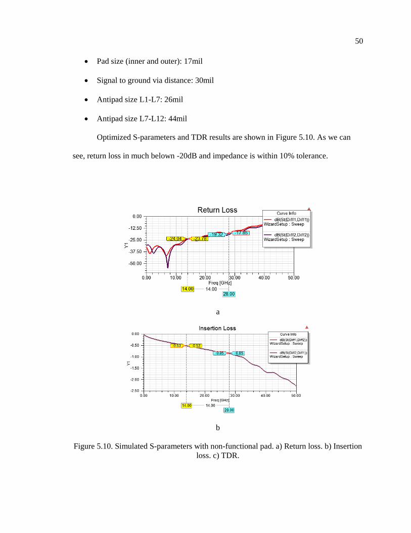
• Pad size (inner and outer): 17mil
• Signal to ground via distance: 30mil
• Antipad size L1-L7: 26mil
• Antipad size L7-L12: 44mil
Optimized S-parameters and TDR results are shown in Figure 5.10. As we can
see, return loss in much belown -20dB and impedance is within 10% tolerance.
a
b
Figure 5.10. Simulated S-parameters with non-functional pad. a) Return loss. b) Insertion
loss. c) TDR.
51
c
Figure 5.10. Simulated S-parameters with non-functional pad. a) Return loss. b) Insertion
loss. c) TDR. (Cont.)
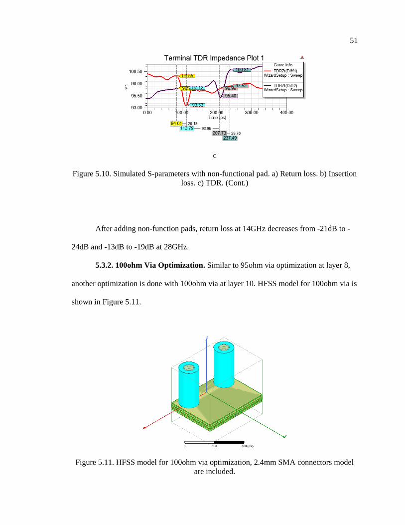
After adding non-function pads, return loss at 14GHz decreases from -21dB to -
24dB and -13dB to -19dB at 28GHz.
5.3.2. 100ohm Via Optimization. Similar to 95ohm via optimization at layer 8,
another optimization is done with 100ohm via at layer 10. HFSS model for 100ohm via is
shown in Figure 5.11.
Figure 5.11. HFSS model for 100ohm via optimization, 2.4mm SMA connectors model
are included.

52
Figure 5.12 shows the geometries for 100ohm vias. Those geometries are
consistent with 95ohm vias. Trace width is 12.75mil at signal-ended area and 9.25mil at
differential area. The distance between two SMA connector (center to center) for one
differential pair is 500mil. Based on the new Dk/Df extraction methodology [20], the
distance for single-ended area should be as short as possible. Therefore, considering
cables diameter, 500mil is the closest distance can be used. There are seven ground vias
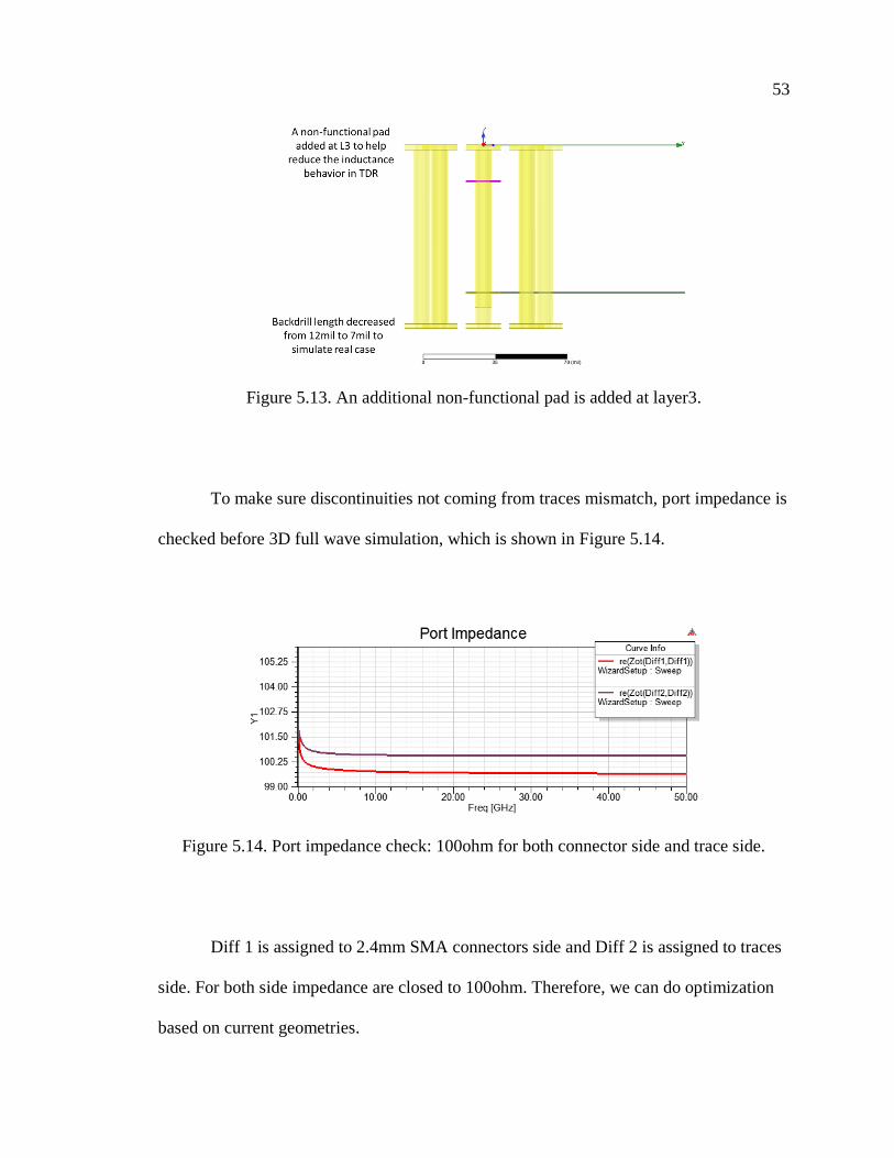
around one signal via. The distance between ground via and signal via is 30mil. A non-
functional pad also added at layer 3 to help reduce high impedance, which is shown in
Figure 5.13.
a b
Figure 5.12. HFSS model geometries. a) 500mil spacing between two connectors. b)
Distance between signal via to ground via is 30mil.
53
Figure 5.13. An additional non-functional pad is added at layer3.
To make sure discontinuities not coming from traces mismatch, port impedance is
checked before 3D full wave simulation, which is shown in Figure 5.14.
Figure 5.14. Port impedance check: 100ohm for both connector side and trace side.
Diff 1 is assigned to 2.4mm SMA connectors side and Diff 2 is assigned to traces
side. For both side impedance are closed to 100ohm. Therefore, we can do optimization
based on current geometries.

54
After sweeping antipad size at adjacent layers, the best results are shown in Figure
5.15.
a
b
c
Figure 5.15. Simulated results from HFSS. (a) Return loss. b) Insertion loss. c) TDR.
55
Return loss at 14GHz is -40dB and even at 28GHz is -18dB. TDR also shows that
impedance is controlled within ±3Ohm comparing with target impedance. Therefore,
summarize geometries are:
• Drill hole size: 7.9mil
• Pad size (inner and outer): 17mil
• Signal to ground via distance: 30mil
• Antipad size L1-L8: 26mil
• Antipad size L9-L12: 34mil
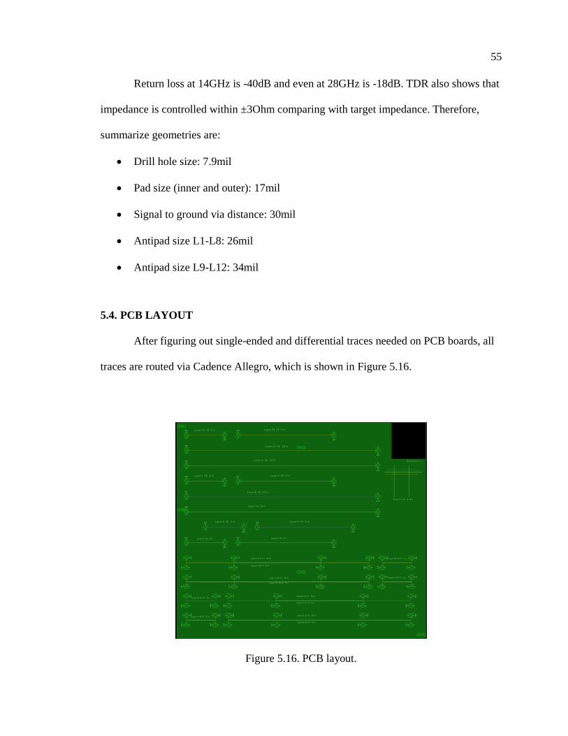
5.4. PCB LAYOUT
After figuring out single-ended and differential traces needed on PCB boards, all
traces are routed via Cadence Allegro, which is shown in Figure 5.16.
Figure 5.16. PCB layout.

56
A 13in × 11.25in PCB is designed. In this PCB board, both single-ended and
differential pairs at layer3, layer5, layer8 and layer11 are included. Besides all testing
traces, there are another two areas are included:
On the top right corner, an 1800mil × 1900mil dielectric area is designed for
doing SPDR measurements. In this area, all copper layers are removed. By comparing
the Df value measured by SPDR measurements and extracted from S-parameters, the
difference will clearly show how does surface roughness impact transmission line loss.
Below the dielectric area, a cross-section area is also designed. Both single-ended and
differential traces at layer8 and layer10 are included this area. Therefore, there is no need
to damage any traces used for testing but just cut the artificial ones.

57
BIBLIOGRAPHY
[1] Stephen H. Hall, Howard L. Heck. “Advanced Signal Integrity for High – Speed
Digital Design” [Online] Available:
http://onlinelibrary.wiley.com/book/10.1002/9780470423899
[2] John David Jackson. Classical Electrodynamics. John Wiley & Sons Ltd. 1962.
[3] Lee, B. “The Impact of Innerlayer Copper Foil Roughness on Signal Integrity”,
Printed Circuit Design and Fab, April 200.
[4] Xinyao Guo, Han Gao, Guangyao Shen, Qian Liu, Victor Khilkevich, James
Drewniak, Soumya De, Scott Hinaga, Douglas Yanagawa, "Design methodology
for behavioral surface roughness model", Electromagnetic Compatibility (EMC)
2016 IEEE International Symposium on, pp. 927-931, 2016.
[5] Djordjevic A.R.; Biljie, R.M.; Likar-Smiljanic, V.D.; Sarkar, T.K., "Wideband
frequency-domain characterization of FR-4 and time-domain causality," in
Electromagnetic Compatibility, IEEE Transactions on , vol.43, no.4, pp.662-667,
Nov. 2001 doi: 10.1109/15.97464.
[6] A.V. Rakov, S. De, M. Y. Koledintseva, S. Hinaga, J. L. Drewniak and R. J.
Stanley, "Quantification of Conductor Surface Roughness Profiles in Printed
Circuit Boards," in IEEE Transactions on Electromagnetic Compatibility, vol.57,
no. 2, pp. 264-273, April 2015.
[7] Ippich, “A Designs Experiment for the Influence of Copper Foils on Impedance,
DC Line Resistance and Insertion Loss,” IPC APEX Expo 2012.
[8] Y. Shlepnev, “Dielectric and Conductor Roughness Models Identification for
Successful PCB and Packaging Interconnect Design up to 50 GHz,” The PCB
Design Magazine 02/2014; 2014(2):12-28.
[9] Koledintseva, M.Y.; Razmadze, A.G.; Gafarov, A.Y.; Soumya De; Drewniak,J.L.;
Hinaga, S., "PCB conductor surface roughness as a layer with effective material
parameters," in Electromagnetic Compatibility (EMC), 2012 IEEE International
Symposium on , vol., no., pp.138-143, 6-10 Aug. 2012.
[10] https://en.wikipedia.org/wiki/Effective_medium_approximations
[11] http:/ningpan.net/publications/151-200/156.pdf

58
[12] S. G. Pytel, G. Barnes, D. Hua, A. Moonshiram, G. Brist, R. Mellitz, S. Hall, and
P. G. Huray, “Dielectric modeling, characterization, and validation up to 40GHz,”
presented at the 11th Signal Propag. on Interconnects Workshop, Genoa, Italy,
May 13–16, 2007.
[13] Deutsch, e.t. “Extraction of ε_r(f) and tanδ(f) for Printed Circuit Board Insulators
Up to 30 GHz Using the Short-Pulse Propagation Technique,” IEEE Transactions
on Advanced Packaging, vol.28, no.1, Feb. 2005.
[14] Lei Hua, Bichen Chen, Shuai Jin, Marina Koledintseva, Jane Lim, Kelvin Qiu,
Rick Brooks, Ji Zhang, Ketan Shringarpure, Jun Fan, "Characterization of PCB
dielectric properties using two striplines on the same board," in Electromagnetic
Proc. IEEE Int. Symp. EMC Raleigh, pp. 809-814, Aug. 4–8, 2014.
[15] S.B. Cohn. “Shielded Coupled-Strip Transmission Line”. IRE Transactions on
Microwave Theory and Techniques. October, 1955.
[16] Harold A. Wheeler, ‘Formulas for Skin Effect’, Proceeding of the I.R.E, Sep
1942.
[17] Jeonghyeon Cho. “Mixed-Mode ABCD Parameters: Theory and Application to
Signal Integrity Analysis of PCB-Level Differential Interconnects”. IEEE
Transactions on Electromagnetic Compatibility. Vol 53 August, 2011.
[18] Paul G. Huray. “Impact of Copper Surface Texture on Loss: A model that
Works”. DesignCon. 2010.
[19] Michael Griesi. “Eletrodeposited Copper Foil Surface Characterization for
Accurate Conductor Loss Modeling”. DesignCon. 2015.
[20] Shaohui Yong, Yuanzhuo Liu, Han Gao, Bichen Chan, Soumya De, Scott Hinaga,
Douglas Yanagawa, James Drewniak, Victor Khikcvich, "Dielectric Dissipation
Factor (DF) Extraction Based on Differential Measurements and 2-D Cross-
sectional Analysis," in Electromagnetic Compatibility (EMC) 2018 IEEE
International Symposium.
[21] X. Sun, T. Huang, L. Ye, Y. Sun, S. Jin, and J. Fan, “Analyzing Multiple Vias in
a Parallel-Plate Pair Based on a Nonorthogonal PEEC Method” IEEE
Transactions on Electromagnetic Compatibility, 2018.
[22] B. Chen, J. He, X. Sun, Y. Guo, S. Jin, and J. Fan, “Differential S-Parameter De-
embedding for 8-Port Network”, 2018 IEEE Symposium on Electromagnetic
Compatibility, Signal Integrity and Power Integrity (EMC, SI & PI), Long
Beach, CA, USA.

59
[23] X. Sun, L. Ye, K. Song, Y. Sun, S. Jin, B. Chen, M. Tsiklauri, X. Ye, and J. Fan
“An Efficient Approach to Find the Truncation Frequency for Transmission Line-
Based Dielectric Material Property Extraction” 2018 IEEE Symposium on
Electromagnetic Compatibility, Signal Integrity and Power Integrity (EMC,
SI&PI), Long Beach, CA, USA.
[24] S. Jin, D. Liu, B. Chen, R. Brooks, K. Qiu, J. Lim, and J. Fan, “Analytical
Equivalent Circuit Modeling for BGA in High-Speed Package” IEEE
Transactions on Electromagnetic Compatibility. Vol. 60, pp 68-76, Feb 2018.
[25] S. Jin, D. Liu, Y. Wang, B. Chen and J. Fan “Parallel Plate Impedance and
Equivalent Inductance Extraction Considering Proximity Effect by a Modal
Approach”, IEEE Transactions on Electromagnetic Compatibility. Vol. 60, pp
1481-1490, Oct 2018.
[26] S. Jin, B. Chen, X. Fang, H. Gao and J. Fan, “Improved “Root-Omega” method
for transmission-line based material property extraction for multilayer PCBs”,
IEEE Trans. On Electromagnetic Compatibility. Vol. 59, pp 1356-1367, Aug
2017.
[27] L. Ye, C. Li, X. Sun, Shuai Jin, B. Chen, X. Ye, and J. Fan, “Thru-Reflect-Line
Calibration technique: error analysis for characteristic impedance variations in the
line standards,” IEEE Trans. On Electromagnetic Compatibility. Dec. 2017.
[28] S. Jin, “Modal based BGA modeling in high-speed package”, dissertation in
Thesis in Missouri University of Science and Technology, 2017.
[29] S. Jin, J. Zhang, J. Lim, K. Qiu, R. Brooks, and J. Fan, “Analytical Equivalent
Circuit Modeling for Multiple Core Vias in a High-Speed Package,” in Proc.
IEEE Int. Symp. EMC, Ottawa, CN, July. 25-29, 2016
[30] B. Chen, M. Tsiklauri, C. Wu, Shuai Jin, J. Fan, X. Ye and B. Samaras,
“Analytical and numerical sensitivity analyses of fixtures de-embedding,” in Proc.
IEEE Int. Symp. EMC, Ottawa, CN, July. 25-29, 2016
[31] S. Jin, X. Fang, B. Chen, H. Gao, X. Ye and J. Fan, “Validating the transmission-
line based material property extraction procedure including surface roughness for
multilayer PCBs using simulations,” in Proc. IEEE Int. Symp. EMC, Ottawa, CN,
July. 25-29, 2016.
[32] S. Jin, J. Zhang and J. Fan, “Optimization of the transition from connector to PCB
board,” in Proc. IEEE Int. Symp. EMC, Aug. 5-9, 2013.

60
VITA
Han Gao received her M.S. degree of Statistics in May 2013 from Rutgers
University, New Brunswick. She joined the EMC Lab for her second M.S degree. She
received her M.S. degree of Electrical Engineering in May 2019 from Missouri
University of Science and Technology. She had a co-op in Cisco Enterprise Switching
Access team from January to December 2017.
Her research interests included signal integrity in high-speed digital system,
surface roughness and dielectric model investigation, lossy material properties, SerDes
characterizations.