high speed optocoupler, 5 mbd, 1 kv/µs dv/dt€¦ · · 2008-10-15high speed optocoupler, 5 mbd,...
TRANSCRIPT
Document Number: 83683 For technical questions, contact: [email protected] www.vishay.comRev. 1.5, 15-Apr-05 1
High Speed Optocoupler,5 MBd, 1 kV/µs dV/dt
SFH6700/01/02/05/11/12/19Vishay Semiconductors
DESCRIPTIONThe SFH67xx high speed optocoupler series consists of aGaAlAs infrared emitting diode, optically coupled with anintegrated photo detector. The detector incorporates aSchmitt-Trigger stage for improved noise immunity. Usingthe enable input, the output can switched to the high ohmicstate, which is necessary for data bus applications. AFaraday shield provides a common mode transient immunityof 1000 V/µ at VCM = 50 V for SFH6700/01/02/05 and2500 V/µ at VCM = 400 V for SFH6711/12/19.The SFH67xx uses an industry standard DIP-8 package.With standard lead bending, creepage distance andclearance of ≥ 7.0 mm with lead bending options 6, 7, and9 ≥ 8 mm are achieved.
FEATURES• Data rate 5.0 MBits/s (2.5 MBit/s over
temperature)• Buffer
• Isolation test voltage, 5300 VRMS for 1.0 s
• TTL, LSTTL and CMOS compatible• Internal shield for very high common mode
transient immunity
• Wide supply voltage range (4.5 to 15 V)• Low input current (1.6 mA to 5 mA)
• Three state output (SFH6700/19)
• Totem pole output (SFH6701/02/11/12)• Open collector output (SFH6705)
• Lead (Pb)-free component
• Component in accordance to RoHS 2002/95/EC andWEEE 2002/96/EC
APPLICATIONS• Industrial control• Replace pulse transformers
• Routine logic interfacing
• Motion/power control• High speed line receiver
• Microprocessor system interfaces
• Computer peripheral interfaces
AGENCY APPROVALS• UL1577, file no. E52744 system code H or J, double
protection• DIN EN 60747-5-2 (VDE 0884)/DIN EN 60747-5-5 pending
available with option 1
NoteFor additional information on the available options refer to option information.
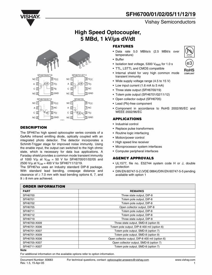
i179073
1
2
3
4
8
7
6
5
VCC
VO
VE
GND
NC
A
C
NC
SFH6700/6719
1
2
3
4
8
7
6
5
VCC
VO
NC
GND
NC
A
C
NC
SFH6701/6711
1
2
3
4
8
7
6
5
VCC
NC
VO
GND
SFH6702/6712
NC
A
C
NC
1
2
3
4
8
7
6
5
VCC
NC
VO
GND
SFH6705
NC
A
C
NC
ORDER INFORMATIONPART REMARKS
SFH6700 Three state output, DIP-8SFH6701 Totem pole output, DIP-8SFH6702 Totem pole output, DIP-8SFH6705 Open collector output, DIP-8SFH6711 Totem pole output, DIP-8SFH6712 Totem pole output, DIP-8SFH6719 Three state output, DIP-8SFH6700-X009 Three state output, SMD-8 (option 9)SFH6701-X006 Totem pole output, DIP-8 400 mil (option 6)SFH6701-X007 Totem pole output, SMD-8 (option 7)SFH6701-X009 Totem pole output, SMD-8 (option 9)SFH6705-X006 Open collector output, DIP-8 400 mil (option 6)SFH6705-X007 Open collector output, SMD-8 (option 7)SFH6711-X007 Totem pole output, SMD-8 (option 7)
www.vishay.com For technical questions, contact: [email protected] Document Number: 836832 Rev. 1.5, 15-Apr-05
SFH6700/01/02/05/11/12/19Vishay Semiconductors High Speed Optocoupler,
5 MBd, 1 kV/µs dV/dt
NoteTamb = 25 °C, unless otherwise specified.Stresses in excess of the absolute maximum ratings can cause permanent damage to the device. Functional operation of the device is not impliedat these or any other conditions in excess of those given in the operational sections of this document. Exposure to absolute maximum ratings forextended periods of the time can adversely affect reliability.
TRUTH TABLE (Positive Logic)
PARTS IR DIODE ENABLE OUTPUT
SFH6700on H Z
off H Z
SFH6719on L H
off L L
SFH6701on H
off L
SFH6702on H
off L
SFH6705on H
off L
SFH6711on H
off L
SFH6712on H
off L
ABSOLUTE MAXIMUM RATINGSPARAMETER TEST CONDITION SYMBOL VALUE UNIT
INPUT
Reverse voltage VR 3.0 V
DC forward current IF 10 mA
Surge forward current t ≤ 1.0 µs IFSM 1.0 A
Power dissipation Pdiss 20 mW
OUTPUT
Supply voltage VCC - 0.5 to + 15 V
Three state enable voltage(SFH6700/19 only) VEN - 0.5 to + 15 V
Output voltage VO - 0.5 to + 15 V
Average output current IO 25 mA
Power dissipation Pdiss 100 mW
COUPLER
Storage temperature range Tstg - 55 to + 125 °C
Ambient temperature range Tamb + 85 °C
Lead soldering temperature t = 10 s Tsld 260 °C
Isolation test voltage VISO 5300 VRMS
Pollution degree 2.0
Creepage distance and clearanceStandard lead bending 7.0 mm
Options 6, 7, 9 8.0 mm
Comparative tracking index per DIN IEC 112/VDE 0303, part 1 175
Isolation resistanceVIO = 500 V, Tamb = 25 °C RIO 1012 Ω
VIO = 500 V, Tamb = 100 °C RIO 1011 Ω
Document Number: 83683 For technical questions, contact: [email protected] www.vishay.comRev. 1.5, 15-Apr-05 3
SFH6700/01/02/05/11/12/19High Speed Optocoupler,
5 MBd, 1 kV/µs dV/dtVishay Semiconductors
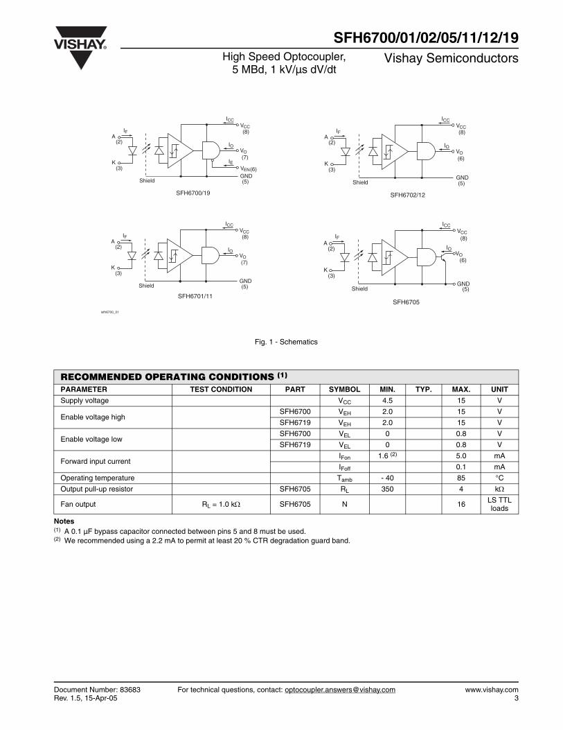
Fig. 1 - Schematics
Notes(1) A 0.1 µF bypass capacitor connected between pins 5 and 8 must be used.(2) We recommended using a 2.2 mA to permit at least 20 % CTR degradation guard band.
RECOMMENDED OPERATING CONDITIONS (1)
PARAMETER TEST CONDITION PART SYMBOL MIN. TYP. MAX. UNIT
Supply voltage VCC 4.5 15 V
Enable voltage highSFH6700 VEH 2.0 15 V
SFH6719 VEH 2.0 15 V
Enable voltage lowSFH6700 VEL 0 0.8 V
SFH6719 VEL 0 0.8 V
Forward input currentIFon 1.6 (2) 5.0 mA
IFoff 0.1 mA
Operating temperature Tamb - 40 85 °C
Output pull-up resistor SFH6705 RL 350 4 kΩ
Fan output RL = 1.0 kΩ SFH6705 N 16 LS TTLloads
isfh6700_01
ICCVCC
VO
IO
IE
IF
VEN(3)
(2)
GNDShield
(8)
(7)
(5)
A
K
SFH6700/19
(6)
ICCVCC
VO
IO
IF
(3)
(2)
GNDShield
(8)
(6)
(5)
A
K
SFH6702/12
ICCVCC
VO
IO
IF
(3)
(2)
GNDShield
(8)A
K
(6)
(5)
SFH6705SFH6701/11
ICCVCC
VO
IO
IF
(3)
(2)
GNDShield
(8)
(7)
(5)
A
K
www.vishay.com For technical questions, contact: [email protected] Document Number: 836834 Rev. 1.5, 15-Apr-05
SFH6700/01/02/05/11/12/19Vishay Semiconductors High Speed Optocoupler,
5 MBd, 1 kV/µs dV/dt
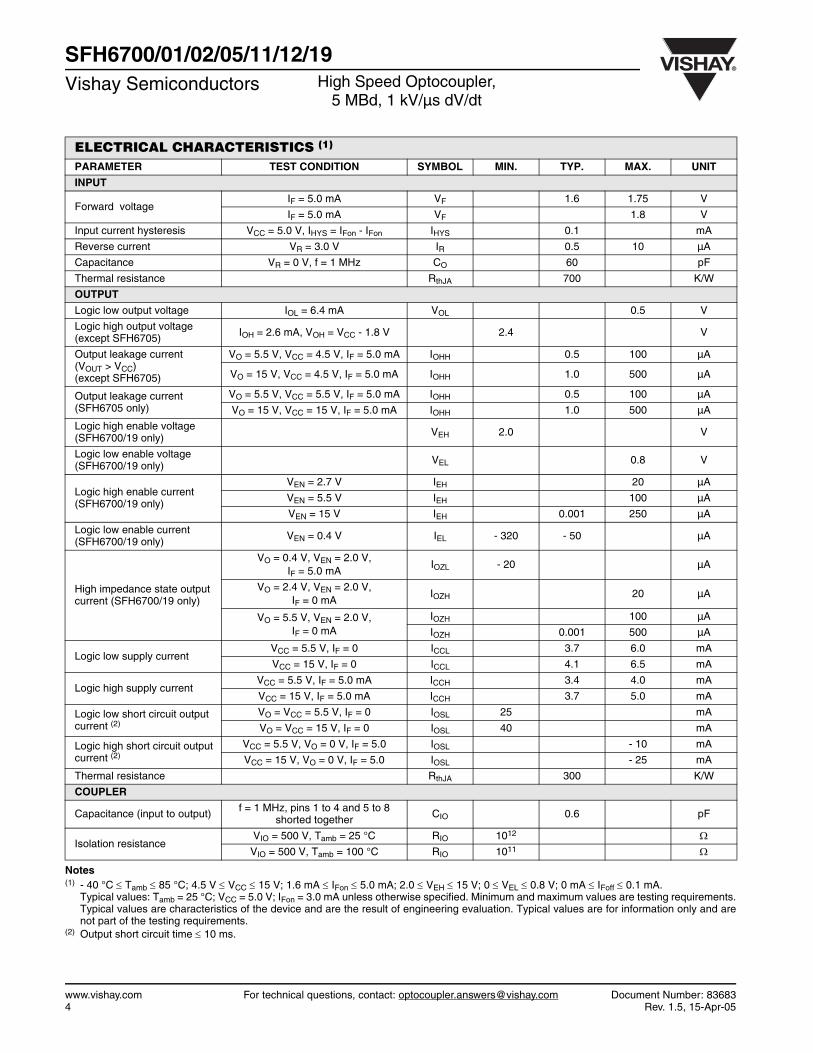
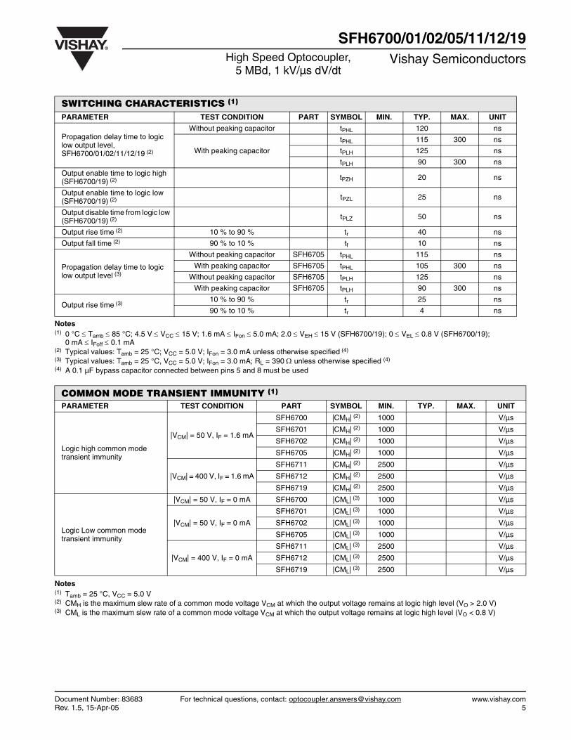
Notes(1) - 40 °C ≤ Tamb ≤ 85 °C; 4.5 V ≤ VCC ≤ 15 V; 1.6 mA ≤ IFon ≤ 5.0 mA; 2.0 ≤ VEH ≤ 15 V; 0 ≤ VEL ≤ 0.8 V; 0 mA ≤ IFoff ≤ 0.1 mA.
Typical values: Tamb = 25 °C; VCC = 5.0 V; IFon = 3.0 mA unless otherwise specified. Minimum and maximum values are testing requirements.Typical values are characteristics of the device and are the result of engineering evaluation. Typical values are for information only and arenot part of the testing requirements.
(2) Output short circuit time ≤ 10 ms.
ELECTRICAL CHARACTERISTICS (1)
PARAMETER TEST CONDITION SYMBOL MIN. TYP. MAX. UNIT
INPUT
Forward voltageIF = 5.0 mA VF 1.6 1.75 V
IF = 5.0 mA VF 1.8 V
Input current hysteresis VCC = 5.0 V, IHYS = IFon - IFon IHYS 0.1 mA
Reverse current VR = 3.0 V IR 0.5 10 µA
Capacitance VR = 0 V, f = 1 MHz CO 60 pF
Thermal resistance RthJA 700 K/W
OUTPUT
Logic low output voltage IOL = 6.4 mA VOL 0.5 V
Logic high output voltage(except SFH6705) IOH = 2.6 mA, VOH = VCC - 1.8 V 2.4 V
Output leakage current(VOUT > VCC)(except SFH6705)
VO = 5.5 V, VCC = 4.5 V, IF = 5.0 mA IOHH 0.5 100 µA
VO = 15 V, VCC = 4.5 V, IF = 5.0 mA IOHH 1.0 500 µA
Output leakage current (SFH6705 only)
VO = 5.5 V, VCC = 5.5 V, IF = 5.0 mA IOHH 0.5 100 µA
VO = 15 V, VCC = 15 V, IF = 5.0 mA IOHH 1.0 500 µA
Logic high enable voltage (SFH6700/19 only) VEH 2.0 V
Logic low enable voltage (SFH6700/19 only) VEL 0.8 V
Logic high enable current (SFH6700/19 only)
VEN = 2.7 V IEH 20 µA
VEN = 5.5 V IEH 100 µA
VEN = 15 V IEH 0.001 250 µA
Logic low enable current (SFH6700/19 only) VEN = 0.4 V IEL - 320 - 50 µA
High impedance state output current (SFH6700/19 only)
VO = 0.4 V, VEN = 2.0 V, IF = 5.0 mA
IOZL - 20 µA
VO = 2.4 V, VEN = 2.0 V, IF = 0 mA
IOZH 20 µA
VO = 5.5 V, VEN = 2.0 V, IF = 0 mA
IOZH 100 µA
IOZH 0.001 500 µA
Logic low supply currentVCC = 5.5 V, IF = 0 ICCL 3.7 6.0 mA
VCC = 15 V, IF = 0 ICCL 4.1 6.5 mA
Logic high supply currentVCC = 5.5 V, IF = 5.0 mA ICCH 3.4 4.0 mA
VCC = 15 V, IF = 5.0 mA ICCH 3.7 5.0 mA
Logic low short circuit output current (2)
VO = VCC = 5.5 V, IF = 0 IOSL 25 mA
VO = VCC = 15 V, IF = 0 IOSL 40 mA
Logic high short circuit output current (2)
VCC = 5.5 V, VO = 0 V, IF = 5.0 IOSL - 10 mA
VCC = 15 V, VO = 0 V, IF = 5.0 IOSL - 25 mA
Thermal resistance RthJA 300 K/W
COUPLER
Capacitance (input to output) f = 1 MHz, pins 1 to 4 and 5 to 8shorted together CIO 0.6 pF
Isolation resistanceVIO = 500 V, Tamb = 25 °C RIO 1012 Ω
VIO = 500 V, Tamb = 100 °C RIO 1011 Ω
Document Number: 83683 For technical questions, contact: [email protected] www.vishay.comRev. 1.5, 15-Apr-05 5
SFH6700/01/02/05/11/12/19High Speed Optocoupler,
5 MBd, 1 kV/µs dV/dtVishay Semiconductors
Notes(1) 0 °C ≤ Tamb ≤ 85 °C; 4.5 V ≤ VCC ≤ 15 V; 1.6 mA ≤ IFon ≤ 5.0 mA; 2.0 ≤ VEH ≤ 15 V (SFH6700/19); 0 ≤ VEL ≤ 0.8 V (SFH6700/19);
0 mA ≤ IFoff ≤ 0.1 mA(2) Typical values: Tamb = 25 °C; VCC = 5.0 V; IFon = 3.0 mA unless otherwise specified (4) (3) Typical values: Tamb = 25 °C, VCC = 5.0 V; IFon = 3.0 mA; RL = 390 Ω unless otherwise specified (4) (4) A 0.1 µF bypass capacitor connected between pins 5 and 8 must be used
Notes(1) Tamb = 25 °C, VCC = 5.0 V(2) CMH is the maximum slew rate of a common mode voltage VCM at which the output voltage remains at logic high level (VO > 2.0 V)(3) CML is the maximum slew rate of a common mode voltage VCM at which the output voltage remains at logic high level (VO < 0.8 V)
SWITCHING CHARACTERISTICS (1)
PARAMETER TEST CONDITION PART SYMBOL MIN. TYP. MAX. UNIT
Propagation delay time to logic low output level, SFH6700/01/02/11/12/19 (2)
Without peaking capacitor tPHL 120 ns
With peaking capacitor
tPHL 115 300 ns
tPLH 125 ns
tPLH 90 300 ns
Output enable time to logic high (SFH6700/19) (2) tPZH 20 ns
Output enable time to logic low (SFH6700/19) (2) tPZL 25 ns
Output disable time from logic low (SFH6700/19) (2) tPLZ 50 ns
Output rise time (2) 10 % to 90 % tr 40 ns
Output fall time (2) 90 % to 10 % tf 10 ns
Propagation delay time to logic low output level (3)
Without peaking capacitor SFH6705 tPHL 115 ns
With peaking capacitor SFH6705 tPHL 105 300 ns
Without peaking capacitor SFH6705 tPLH 125 ns
With peaking capacitor SFH6705 tPLH 90 300 ns
Output rise time (3)10 % to 90 % tr 25 ns
90 % to 10 % tr 4 ns
COMMON MODE TRANSIENT IMMUNITY (1)
PARAMETER TEST CONDITION PART SYMBOL MIN. TYP. MAX. UNIT
Logic high common modetransient immunity
|VCM| = 50 V, IF = 1.6 mA
SFH6700 |CMH| (2) 1000 V/µs
SFH6701 |CMH| (2) 1000 V/µs
SFH6702 |CMH| (2) 1000 V/µs
SFH6705 |CMH| (2) 1000 V/µs
|VCM| = 400 V, IF = 1.6 mA
SFH6711 |CMH| (2) 2500 V/µs
SFH6712 |CMH| (2) 2500 V/µs
SFH6719 |CMH| (2) 2500 V/µs
Logic Low common modetransient immunity
|VCM| = 50 V, IF = 0 mA SFH6700 |CML| (3) 1000 V/µs
|VCM| = 50 V, IF = 0 mA
SFH6701 |CML| (3) 1000 V/µs
SFH6702 |CML| (3) 1000 V/µs
SFH6705 |CML| (3) 1000 V/µs
|VCM| = 400 V, IF = 0 mA
SFH6711 |CML| (3) 2500 V/µs
SFH6712 |CML| (3) 2500 V/µs
SFH6719 |CML| (3) 2500 V/µs
www.vishay.com For technical questions, contact: [email protected] Document Number: 836836 Rev. 1.5, 15-Apr-05
SFH6700/01/02/05/11/12/19Vishay Semiconductors High Speed Optocoupler,
5 MBd, 1 kV/µs dV/dt
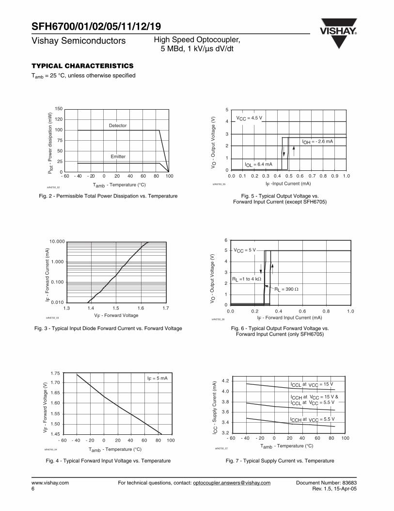
TYPICAL CHARACTERISTICS Tamb = 25 °C, unless otherwise specified
Fig. 2 - Permissible Total Power Dissipation vs. Temperature
Fig. 3 - Typical Input Diode Forward Current vs. Forward Voltage
Fig. 4 - Typical Forward Input Voltage vs. Temperature
Fig. 5 - Typical Output Voltage vs.Forward Input Current (except SFH6705)
Fig. 6 - Typical Output Forward Voltage vs.Forward Input Current (only SFH6705)
Fig. 7 - Typical Supply Current vs. Temperature
isfh6700_02Tamb - Temperature (°C)
Emitter
Detector
150
120
100
75
50
25
0- 60 100806040200- 20- 40
Pto
t-P
ower
diss
ipat
ion
(mW
)
isfh6700_03VF - Forward Voltage
I F-
For
war
dC
urre
nt (
mA
)
0.010
0.100
1.000
10.000
1.3 1.4 1.5 1.6 1.7
isfh6700_04
- 60 - 40 - 20 0 20 40 60 80 1001.45
1.50
1.55
1.60
1.65
1.70
1.75
VF
-F
orw
ard
Vol
tage
(V
)
IF = 5 mA
Tamb - Temperature (°C)
isfh6700_05
0
1
2
3
4
5
0.0 0.1 0.2 0.3 0.4 0.5 0.6 0.7 0.8 0.9 1.0
IF -Input Current (mA)
VO
-O
utp
ut
Vo
ltag
e (
V)
IOL = 6.4 mA
IOH = - 2.6 mA
VCC = 4.5 V
isfh6700_06
0
1
2
3
4
5
6
0.0 0.2 0.4 0.6 0.8 1.0IF - Forward Input Current (mA)
VO
-O
utpu
tVol
tage
(V
)
RL =1 to 4 kΩ
VCC = 5 V
RL = 390 Ω
isfh6700_07
- 60 - 40 - 20 0 20 40 60 80 1003.2
3.4
3.6
3.8
4.0
4.2
I CC
-S
uppl
yC
uren
t (m
A)
ICCL at VCC = 15 V
ICCH at VCC = 15 V &ICCL at VCC = 5.5 V
ICCH at VCC = 5.5 V
Tamb - Temperature (°C)
Document Number: 83683 For technical questions, contact: [email protected] www.vishay.comRev. 1.5, 15-Apr-05 7
SFH6700/01/02/05/11/12/19High Speed Optocoupler,
5 MBd, 1 kV/µs dV/dtVishay Semiconductors
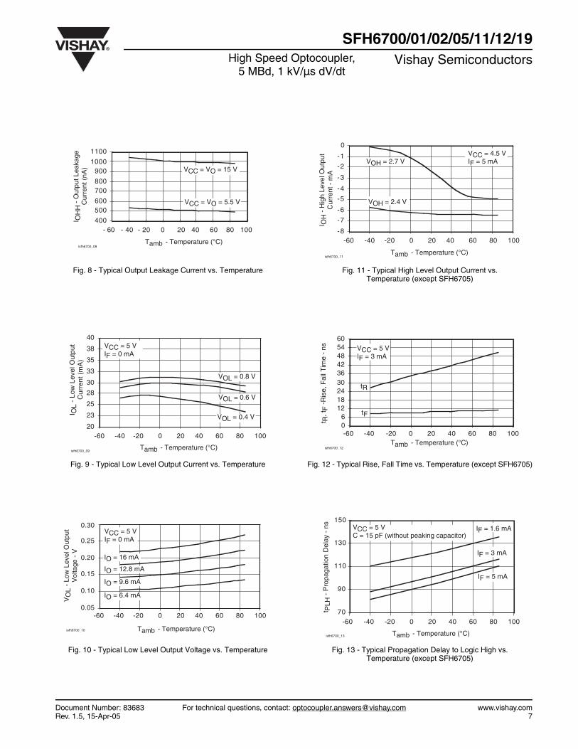
Fig. 8 - Typical Output Leakage Current vs. Temperature
Fig. 9 - Typical Low Level Output Current vs. Temperature
Fig. 10 - Typical Low Level Output Voltage vs. Temperature
Fig. 11 - Typical High Level Output Current vs.Temperature (except SFH6705)
Fig. 12 - Typical Rise, Fall Time vs. Temperature (except SFH6705)
Fig. 13 - Typical Propagation Delay to Logic High vs.Temperature (except SFH6705)
isfh6700_08
- 20 0 20 40 60 80 100400
500600
700800
9001000
1100
- 60 - 40
I OH
H-
Out
putL
eaka
geC
urre
nt (
nA) VCC = VO = 15 V
VCC = VO = 5.5 V
Tamb - Temperature (°C)
isfh6700_09
-20 0 20 40 60 80 10020
23
25
28
30
33
35
38
40
-60 -40
I OL
-Lo
wLe
velO
utpu
tC
urre
nt (
mA
)
VCC = 5 VIF = 0 mA
VOL = 0.6 V
VOL = 0.4 V
VOL = 0.8 V
Tamb - Temperature (°C)
isfh6700_10
-60 -40 -20 0 20 40 60 80 1000.05
0.10
0.15
0.20
0.25
0.30
VO
L-
Low
Leve
lOut
put
Vol
tage
-V
IO = 16 mA
IO = 12.8 mA
IO = 9.6 mA
IO = 6.4 mA
VCC = 5 VIF = 0 mA
Tamb - Temperature (°C)
isfh6700_11
-60 -40 -20 0 20 40 60 80 100-8
-7
-6
-5
-4
-3
-2
-1
0
I OH
-H
igh
Leve
lOut
put
Cur
rent
-m
A
VOH = 2.4 V
VCC = 4.5 VIF = 5 mAVOH = 2.7 V
Tamb - Temperature (°C)
isfh6700_12
-60 -40 -20 0 20 40 60 80 10006
121824303642485460
t R,t
F-R
ise,
Fal
lTim
e-
ns
tR
tF
VCC = 5 VIF = 3 mA
Tamb - Temperature (°C)
isfh6700_13
-60 -40 -20 0 20 40 60 80 100
t PLH
-P
ropa
gatio
nD
elay
-ns
70
90
110
130
150VCC = 5 VC = 15 pF (without peaking capacitor)
IF = 3 mA
IF = 5 mA
IF = 1.6 mA
Tamb - Temperature (°C)
www.vishay.com For technical questions, contact: [email protected] Document Number: 836838 Rev. 1.5, 15-Apr-05
SFH6700/01/02/05/11/12/19Vishay Semiconductors High Speed Optocoupler,
5 MBd, 1 kV/µs dV/dt
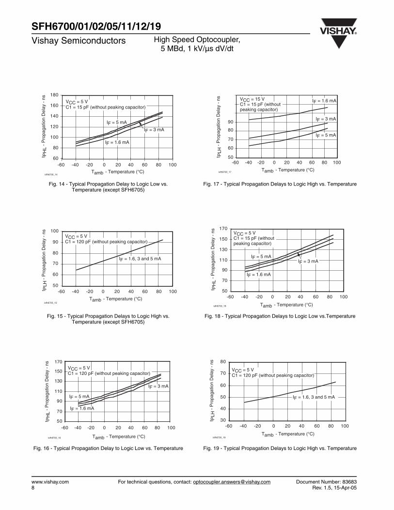
Fig. 14 - Typical Propagation Delay to Logic Low vs.Temperature (except SFH6705)
Fig. 15 - Typical Propagation Delays to Logic High vs.Temperature (except SFH6705)
Fig. 16 - Typical Propagation Delay to Logic Low vs. Temperature
Fig. 17 - Typical Propagation Delays to Logic High vs. Temperature
Fig. 18 - Typical Propagation Delays to Logic Low vs.Temperature
Fig. 19 - Typical Propagation Delays to Logic High vs. Temperature
isfh6700_14
-60 -40 -20 0 20 40 60 80 100
t PH
L-
Pro
paga
tion
Del
ay-
ns
60
80
100
120
140
160
180VCC = 5 VC1 = 15 pF (without peaking capacitor)
IF = 5 mA
IF = 3 mA
IF = 1.6 mA
Tamb - Temperature (°C)
isfh6700_15
-60 -40 -20 0 20 40 60 80 100t PLH
-P
ropa
gatio
nD
elay
-ns
50
60
70
80
90
100VCC = 5 VC1 = 120 pF (without peaking capacitor)
IF = 1.6, 3 and 5 mA
Tamb - Temperature (°C)
isfh6700_16
-60 -40 -20 0 20 40 60 80 100
t PH
L-
Pro
paga
tion
Del
ay-
ns
50
70
90
110
130
150
170VCC = 5 VC1 = 120 pF (without peaking capacitor)
IF = 3 mA
IF = 5 mA
IF = 1.6 mA
Tamb - Temperature (°C)
isfh6700_17
-60 -40 -20 0 20 40 60 80 100
t PLH
-P
ropa
gatio
nD
elay
-ns
50
60
70
80
90
VCC = 15 VC1 = 15 pF (withoutpeaking capacitor)
IF = 1.6 mA
IF = 3 mA
IF = 5 mA
Tamb - Temperature (°C)
isfh6700_18
-60 -40 -20 0 20 40 60 80 100
t PH
L-
Pro
paga
tion
Del
ay-
ns
50
70
90
110
130
150
170VCC = 5 VC1 = 15 pF (withoutpeaking capacitor)
IF = 5 mA
IF = 1.6 mA
IF = 3 mA
Tamb - Temperature (°C)
isfh6700_19
-60 -40 -20 0 20 40 60 80 100
t PLH
-P
ropa
gatio
nD
elay
-ns
30
40
50
60
70
80
VCC = 5 VC1 = 120 pF (without peaking capacitor)
IF = 1.6, 3 and 5 mA
Tamb - Temperature (°C)
Document Number: 83683 For technical questions, contact: [email protected] www.vishay.comRev. 1.5, 15-Apr-05 9
SFH6700/01/02/05/11/12/19High Speed Optocoupler,
5 MBd, 1 kV/µs dV/dtVishay Semiconductors
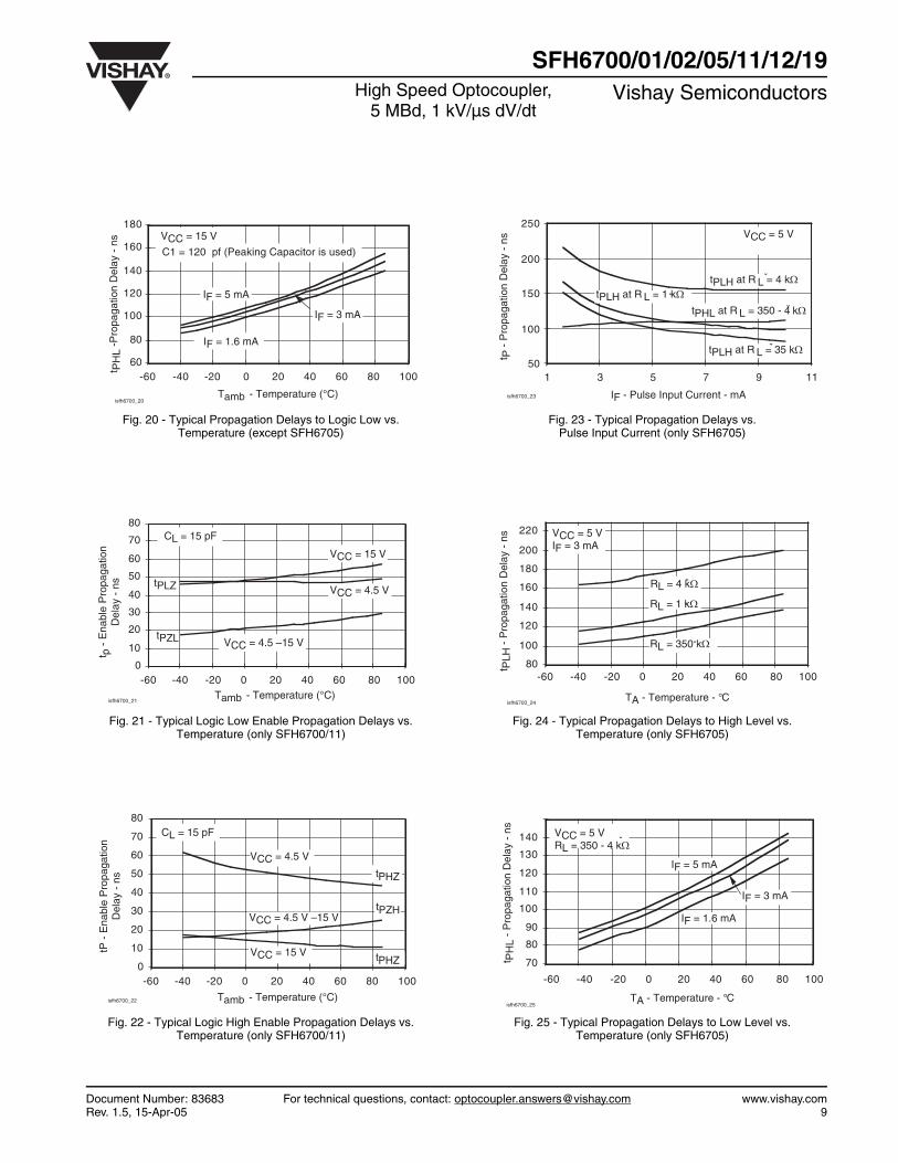
Fig. 20 - Typical Propagation Delays to Logic Low vs.Temperature (except SFH6705)
Fig. 21 - Typical Logic Low Enable Propagation Delays vs.Temperature (only SFH6700/11)
Fig. 22 - Typical Logic High Enable Propagation Delays vs. Temperature (only SFH6700/11)
Fig. 23 - Typical Propagation Delays vs.Pulse Input Current (only SFH6705)
Fig. 24 - Typical Propagation Delays to High Level vs.Temperature (only SFH6705)
Fig. 25 - Typical Propagation Delays to Low Level vs.Temperature (only SFH6705)
isfh6700_20
60
80
100
120
140
160
180
-60 -40 -20 0 20 40 60 80 100
VCC = 15 V
C1 = 120 pf (Peaking Capacitor is used)
IF = 5 mA
t PH
L-P
ropa
gatio
nD
elay
-ns
IF = 3 mA
IF = 1.6 mA
Tamb - Temperature (°C)
isfh6700_21
t p-
Ena
ble
Pro
paga
tion
Del
ay-
ns
0
10
20
30
40
50
60
70
80
-60 -40 -20 0 20 40 60 80 100
CL = 15 pF
VCC = 15 V
VCC = 4.5 –15 VtPZL
tPLZ VCC = 4.5 V
Tamb - Temperature (°C)
isfh6700_22
0
10
20
30
40
50
60
70
80
-60 -40 -20 0 20 40 60 80 100
CL = 15 pF
tPHZ
tPZH
tPHZ
VCC = 4.5 V
tP-
Ena
ble
Pro
paga
tion
Del
ay-
ns
VCC = 4.5 V –15 V
VCC = 15 V
Tamb - Temperature (°C)
isfh6700_23 IF - Pulse Input Current - mA
50
100
150
200
250
1 3 5 7 9 11
VCC = 5 V
tPLH at R L = 4 kΩˇ
ˇˇ
ˇ
t P-
Pro
paga
tion
Del
ay-
ns
tPHL at R L = 350 - 4 kΩ
tPLH at R L = 35 kΩ
tPLH at R L = 1 kΩ
isfh6700_24
-60 -40 -20 0 20 40 60 80 100
TA - Temperature - °C
80
100
120
140
160
180
200
220 VCC = 5 VIF = 3 mA
ˇ
ˇ
ˇ
t PLH
-P
ropa
gatio
nD
elay
-ns
RL = 4 kΩ
RL = 1 kΩ
RL = 350 kΩ
isfh6700_25
-60 -40 -20 0 20 40 60 80 100
TA - Temperature - °C
t PH
L-
Pro
paga
tion
Del
ay-
ns
70
80
90
100
110
120
130
140 ˇVCC = 5 VRL = 350 - 4 kΩ
IF = 5 mA
IF = 3 mA
IF = 1.6 mA
www.vishay.com For technical questions, contact: [email protected] Document Number: 8368310 Rev. 1.5, 15-Apr-05
SFH6700/01/02/05/11/12/19Vishay Semiconductors High Speed Optocoupler,
5 MBd, 1 kV/µs dV/dt
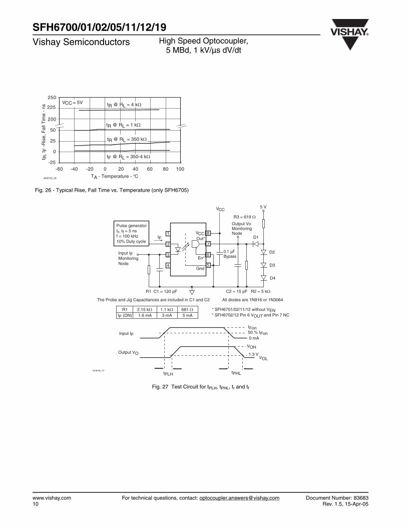
Fig. 26 - Typical Rise, Fall Time vs. Temperature (only SFH6705)
Fig. 27 Test Circuit for tPLH, tPHL, tr and tf
isfh6700_26
-25
0
25
50
-60 -40 -20 0 20 40 60 80 100
250
225 tR @ RL = 4 kΩVCC = 5V
200
t R,t
F-R
ise,
Fal
lTim
e-
ns
TA - Temperature - °C
tR @ RL = 1 kΩ
tR @ RL = 350 kΩ
tF @ RL = 350-4 kΩ
isfh6700_27
All diodes are 1N916 or 1N3064The Probe and Jig Capacitances are included in C1 and C2
* SFH6701/02/11/12 without VEN* SFH6702/12 Pin 6 VOUT and Pin 7 NC
Pulse generatortr, tf = 5 nsf = 100 kHz10% Duty cycle
1
2
3
4
Input IFMonitoringNode
C1 = 120 pF C2 = 15 pF R2 = 5 kΩ
R3 = 619 Ω
VCCOut*
En*
Gnd
VCC5 V
Output VoMonitoringNode
D1
D2
D3
D4
IF
R1
0.1 µFBypass
8
7
6
5
R1IF (ON)
2.15 kΩ1.6 mA
681 Ω5 mA
1.1 kΩ3 mA
Input IF
Output VO
IFon50 % IFon0 mA
VOH
1.3 V
tPLH tPHL
VOL
Document Number: 83683 For technical questions, contact: [email protected] www.vishay.comRev. 1.5, 15-Apr-05 11
SFH6700/01/02/05/11/12/19High Speed Optocoupler,
5 MBd, 1 kV/µs dV/dtVishay Semiconductors
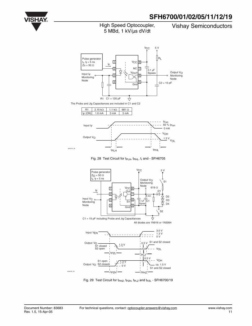
Fig. 28 Test Circuit for tPLH, tPHL, tr and - SFH6705
Fig. 29 Test Circuit for tPHZ, tPZH, tPLZ and tPZL - SFH6700/19
isfh6700_28
The Probe and Jig Capacitances are included in C1 and C2
R1IF (ON)
2.15 kΩ1.6 mA
681 Ω5 mA
1.1 kΩ3 mA
Input IF
Output VO
IFon50 % IFon0 mA
VOH
1.3 V
tPLH tPHL
VOL
1
2
3
4 C2 = 15 pFGnd
0.1 µFBypass
8
7
6
5
C1 = 120 pF
VCC
VOUT
VCC
IF
R1
RL
5 V
NC
Input IFMonitoringNode
Output VOMonitoringNode
Pulse generatortr, tf = 5 nsZo = 50 Ω
isfh6700_29
Output VO
VOL
Output VO
VOH
tPZL tPLZ
S1 and S2 closed
S1 closedS2 open
1.3 V0.5 V
S1 and S2 closedca. 1.5 V
S1 openS2 closed
tPZH tPHZ
1.3 V
0 V
0.5 V
Input VEN3.0 V1.3 V0 V
1
2
3
4
6
7
8VCCOut
En
Gnd
VCC 5 V
D1
D2D3D4
All diodes are 1N916 or 1N3064
IF619 Ω
C1
S1
S2
C1 = 15 pF including Probe and Jig Capacitances
5 kΩ
0.1 µFBypass
Pulse generatorZO = 50 Ωtr, tf = 5 ns
Input VCMonitoringNode
Output VOMonitoringNode
5
www.vishay.com For technical questions, contact: [email protected] Document Number: 8368312 Rev. 1.5, 15-Apr-05
SFH6700/01/02/05/11/12/19Vishay Semiconductors High Speed Optocoupler,
5 MBd, 1 kV/µs dV/dt
Fig. 30 Test Circuit for Common Mode Transient Immunity and Typical Waveforms - SFH6700/01/02/11/12/19
Fig. 31 Test Circuit for Common Mode Transient Immunity and Typical Waveforms - SFH6705
isfh6700_30
0.1 µFBypass
Output VOMonitoringNode
1
2
3
4
6
7
8VccOut*
En*
Gnd
VCC
A
BR
Pulse Generator+ –
VCM
* SFH6701/02/11/12 without VEN* SFH6702/12 Pin 6 VOUT and Pin 7 NC
5
Output VO
VCM400 V / 50 V
Switch at A: IF = 1.6 mA
0 V
VOHVO (min.)
VOLVO (max.)
Switch at B: IF = 0 mA
isfh6700_31
Output VO
VCM
50 V
Switch at A: IF = 1.6 mA
0 V
VOHVO (min)
VOLVO (max)
Switch at B: IF = 0 mA
0.1μFBypass
Output VOMonitoringNode
1
2
3
4
6
7
8
Pulse Generator VCM
5
Out
Gnd
VCC
A
BR
+ –
RL
5 V
n.c.
Document Number: 83683 For technical questions, contact: [email protected] www.vishay.comRev. 1.5, 15-Apr-05 13
SFH6700/01/02/05/11/12/19High Speed Optocoupler,
5 MBd, 1 kV/µs dV/dtVishay Semiconductors
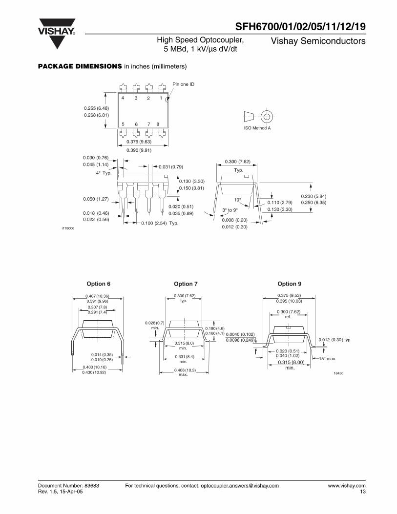
PACKAGE DIMENSIONS in inches (millimeters)
i178006
Pin one ID
0.255 (6.48)
0.268 (6.81)
0.379 (9.63)
0.390 (9.91)
0.030 (0.76)
0.045 (1.14)
4° Typ.
0.100 (2.54) Typ.
10°
3° to 9°
0.300 (7.62)
Typ.
0.018 (0.46)0.022 (0.56) 0.008 (0.20)
0.012 (0.30)
0.110 (2.79)
0.130 (3.30)
0.130 (3.30)
0.150 (3.81)
0.020 (0.51)
0.035 (0.89)
0.230 (5.84)0.250 (6.35)
4 3 2 1
0.031(0.79)
0.050 (1.27)
5 6 7 8ISO Method A
min.0.315 (8.00)
0.020 (0.51)0.040 (1.02)
0.300 (7.62)ref.
0.375 (9.53)0.395 (10.03)
0.012 (0.30) typ.0.0040 (0.102)0.0098 (0.249)
15° max.
Option 9
0.014 (0.35)0.010 (0.25)
0.400 (10.16)0.430 (10.92)
0.307 (7.8)0.291 (7.4)
0.407 (10.36)0.391 (9.96)
Option 6
0.315 (8.0)min.
0.300 (7.62)typ.
0.180 (4.6)0.160 (4.1)
0.331 (8.4)min.
0.406 (10.3)max.
0.028 (0.7)min.
Option 7
18450
www.vishay.com For technical questions, contact: [email protected] Document Number: 8368314 Rev. 1.5, 15-Apr-05
SFH6700/01/02/05/11/12/19Vishay Semiconductors High Speed Optocoupler,
5 MBd, 1 kV/µs dV/dt
OZONE DEPLETING SUBSTANCES POLICY STATEMENTIt is the policy of Vishay Semiconductor GmbH to
1. Meet all present and future national and international statutory requirements.2. Regularly and continuously improve the performance of our products, processes, distribution and operating systems with
respect to their impact on the health and safety of our employees and the public, as well as their impact on the environment.
It is particular concern to control or eliminate releases of those substances into the atmosphere which are known as ozonedepleting substances (ODSs).
The Montreal Protocol (1987) and its London Amendments (1990) intend to severely restrict the use of ODSs and forbid their usewithin the next ten years. Various national and international initiatives are pressing for an earlier ban on these substances.
Vishay Semiconductor GmbH has been able to use its policy of continuous improvements to eliminate the use of ODSs listed inthe following documents.
1. Annex A, B and list of transitional substances of the Montreal Protocol and the London Amendments respectively.2. Class I and II ozone depleting substances in the Clean Air Act Amendments of 1990 by the Environmental Protection Agency
(EPA) in the USA3. Council Decision 88/540/EEC and 91/690/EEC Annex A, B and C (transitional substances) respectively.
Vishay Semiconductor GmbH can certify that our semiconductors are not manufactured with ozone depleting substances and donot contain such substances.
We reserve the right to make changes to improve technical design and may do so without further notice.
Parameters can vary in different applications. All operating parameters must be validated for each customer application by the customer. Should the buyer use Vishay Semiconductors products for any unintended or unauthorized application, the buyer shall
indemnify Vishay Semiconductors against all claims, costs, damages, and expenses, arising out of, directly or indirectly, any claim of personal damage, injury or death associated with such unintended or unauthorized use.
Vishay Semiconductor GmbH, P.O.B. 3535, D-74025 Heilbronn, Germany
Document Number: 91000 www.vishay.comRevision: 18-Jul-08 1
Disclaimer
Legal Disclaimer NoticeVishay
All product specifications and data are subject to change without notice.
Vishay Intertechnology, Inc., its affiliates, agents, and employees, and all persons acting on its or their behalf(collectively, “Vishay”), disclaim any and all liability for any errors, inaccuracies or incompleteness contained hereinor in any other disclosure relating to any product.
Vishay disclaims any and all liability arising out of the use or application of any product described herein or of anyinformation provided herein to the maximum extent permitted by law. The product specifications do not expand orotherwise modify Vishay’s terms and conditions of purchase, including but not limited to the warranty expressedtherein, which apply to these products.
No license, express or implied, by estoppel or otherwise, to any intellectual property rights is granted by thisdocument or by any conduct of Vishay.
The products shown herein are not designed for use in medical, life-saving, or life-sustaining applications unlessotherwise expressly indicated. Customers using or selling Vishay products not expressly indicated for use in suchapplications do so entirely at their own risk and agree to fully indemnify Vishay for any damages arising or resultingfrom such use or sale. Please contact authorized Vishay personnel to obtain written terms and conditions regardingproducts designed for such applications.
Product names and markings noted herein may be trademarks of their respective owners.