graphene and boron nitride lateral heterostructures for ... · graphene and boron nitride lateral...
TRANSCRIPT
LETTERdoi:10.1038/nature11408
Graphene and boron nitride lateral heterostructuresfor atomically thin circuitryMark P. Levendorf1*, Cheol-Joo Kim1*, Lola Brown1, Pinshane Y. Huang2, Robin W. Havener2, David A. Muller2,3 & Jiwoong Park1,3
Precise spatial control over the electrical properties of thin films isthe key capability enabling the production of modern integratedcircuitry. Although recent advances in chemical vapour depositionmethods have enabled the large-scale production of both intrinsicand doped graphene1–6, as well as hexagonal boron nitride (h-BN)7–10,controlled fabrication of lateral heterostructures in these trulyatomically thin systems has not been achieved. Graphene/h-BNinterfaces are of particular interest, because it is known that areasof different atomic compositions may coexist within continuousatomically thin films5,10 and that, with proper control, the bandgapand magnetic properties can be precisely engineered11–13. However,previously reported approaches for controlling these interfaces havefundamental limitations and cannot be easily integrated with con-ventional lithography14–16
. Here we report a versatile and scalableprocess, which we call ‘patterned regrowth’, that allows for thespatially controlled synthesis of lateral junctions between electricallyconductive graphene and insulating h-BN, as well as betweenintrinsic and substitutionally doped graphene. We demonstrate thatthe resulting films form mechanically continuous sheets across theseheterojunctions. Conductance measurements confirm laterallyinsulating behaviour for h-BN regions, while the electrical behaviourof both doped and undoped graphene sheets maintain excellentproperties, with low sheet resistances and high carrier mobilities.Our results represent an important step towards developingatomically thin integrated circuitry and enable the fabricationof electrically isolated active and passive elements embedded incontinuous, one-atom-thick sheets, which could be manipulatedand stacked to form complex devices at the ultimate thickness limit.
Figure 1a summarizes our approach for the patterned regrowth andcharacterization. After growing the first film of graphene (G1, superscriptrepresenting the growth order), we then deposit a protective layer ofphotoresist and pattern away unwanted areas. Next we grow a secondlayer of graphene or h-BN (G2/h-BN2) and transfer the hybrid film ontothe desired substrate for further characterization. All of our growths areperformed on Cu foil using standard literature recipes for both grapheneand h-BN growths4,5,8. Introducing dopant gases during any graphenegrowth stage allows us to produce both intrinsic graphene (i-G; H2 1
CH4) and n-doped graphene (n-G; NH3 1 H2 1 CH4) in a single processrun (see Supplementary Information). Figure 1b shows optical images ofthe Cu growth substrate at different steps of the process. After patterningthe first graphene layer, the substrate was heated to 135 uC in air toenhance the contrast, as is shown in Fig. 1b (left panel); the areas ofCu protected by i-G1 remain unoxidized whereas the unprotected areasdo not17. Figure 1b (right panel) shows the same foil after reduction ofCuOx and subsequent synthesis of the second graphene, and demon-strates the homogeneity of the Cu/graphene substrate. Before furthercharacterization, the presence of graphene is confirmed using micro-Raman spectroscopy (see Supplementary Information).
The fidelity of the transferred pattern and the quality of the junctionsformed by our method were studied using dark-field transmission
electron microscopy (DF-TEM)18,19, where use of a specific objectiveaperture filter allows imaging of areas with corresponding latticeorientations. Multiple such images can then be coloured and overlaidto form a complete map of the film, resolving the grain structure andnumber of layers with nanometre-scale resolution, both near to andaway from the junction area. Figure 1c shows a composite image of agraphene sample that includes both the first and second grown areas aswell as the junction between the two. For this, growths of i-G1/i-G2
were transferred onto 10-nm-thick Si3N4 TEM membranes. Both G1
and G2 regions (see inset to Fig. 1c) comprise single crystals of similarsizes, which indicates that the polycrystalline structure of the grapheneis determined mainly by the synthesis conditions rather than thegrowth order, and also that the structure of the first grown grapheneis unaffected by our patterned regrowth. Significantly, the location ofthe junction closely follows the designed pattern within the resolutionof our instrument (partially outlined area in Fig. 1c; see SupplementaryInformation).
Our DF-TEM data and electrical characterization, in addition to thegrowth conditions, suggest that the junction between G1 and G2 areasare laterally connected. Our recent work20 has shown that a more-reactive growth environment produces graphene–graphene grainboundaries with high-quality lateral connections and minimal inter-domain electrical resistance, whereas a less-reactive growth environ-ment results in poorly connected or even overlapped junctions. In ourpatterned regrowth process, we therefore use highly reactive growthconditions. DF-TEM images of the junction areas indeed show high-quality, continuous growth of graphene between G1 and G2 areas(Fig. 1d), indicating that the crystallinity is maintained uniformly acrossthis region without amorphous carbon or voids, within the spatialresolution of DF-TEM (around 10 nm). Furthermore, the electricalcharacterization across these junctions shows a low junction resistance,similar to that of the high-quality, laterally connected graphene grainboundaries reported in ref. 20.
We also find a highly reactive environment promotes uniformlateral connectivity through increased nucleation at the junction area.In Fig. 1e, we plot grain size as a function of position within the boxindicated in Fig. 1c. While both G1 and G2 regions show average grainsizes of about 1.7mm, near the junction they are much smaller (themean is approximately 0.33mm). The moving average (Fig. 1e, redline) shows that the width of this area with smaller grains is approxi-mately 2mm, comparable to the average G1 and G2 grain size. This, inaddition to the increased density of small bilayer areas (bright spots inFig. 1c and d), suggests that the junction between G1 and G2 is formedby graphene that has nucleated and grown in the junction area ratherthan by direct stitching between grains nucleated away from the junc-tion area. This suggests edge-nucleated growth, which is similar to a‘‘seeding’’ effect reported previously21–23. In contrast, regrowth underless-reactive conditions that provide slower growth do not producewell-connected junctions in either graphene/graphene and graphene/h-BN films (see Supplementary Information).
*These authors contributed equally to this work.
1Department of Chemistry and Chemical Biology, Cornell University, Ithaca, New York 14853, USA. 2School of Applied and Engineering Physics, Cornell University, Ithaca, New York 14853, USA. 3KavliInstitute at Cornell for Nanoscale Science, Ithaca, New York 14853, USA.
3 0 A U G U S T 2 0 1 2 | V O L 4 8 8 | N A T U R E | 6 2 7
Macmillan Publishers Limited. All rights reserved©2012

The technique described above is also applicable to the formation ofinsulator–metal lateral junctions using graphene and h-BN (Fig. 2),which we now discuss (see Methods). Figure 2a shows a false-colourDF-TEM image of a single layer h-BN sheet—as confirmed by Ramanspectroscopy and X-ray photoelectron spectroscopy (see Supplemen-tary Information)—with relatively large domains in excess of 1mm.Electron diffraction also shows that the film consists of single crystalswith hexagonal lattice structures (Fig. 2a, inset). This h-BN growth,however, yields films that are mechanically discontinuous, as indicatedby the dark lines in Fig. 2a (arrows; also visible in bright-field TEM,see Supplementary Information). Instead, h-BN grown under more-reactive conditions (higher precursor flow rate, see Methods) results ina continuous film, while exhibiting all the known characteristics ofh-BN sheets. This is confirmed by the X-ray photoelectron spectro-scopy data in Fig. 2c (upper panels; B and N in a 1:1.08 atomic ratio)and Raman spectroscopy (lower panel; h-BN peak).
Careful control over the length of the h-BN2 growth allows for thesynthesis of i-G1/h-BN2 sheets with high pattern fidelity, as shown bythe optical image in Fig. 2b. The darker regions indicate areas of i-G1
(stronger absorption), whereas the lighter regions are comprised ofh-BN2. This, as well as the two-dimensional Raman image (inset inFig. 2b) of the graphene 2D band intensity, confirms the successfulpattern transfer to the i-G1/h-BN2 hybrid sheet. Furthermore, DF-TEM of suspended films confirms a sharp junction, as is shown inFig. 2d, where the grains of the i-G1 growth (lower, coloured half) endabruptly at the interface with the h-BN2 (upper half). Both the bright-field TEM (Supplementary Information) and scanning electron micro-scopy (SEM) images (Fig. 2e) show a mechanically continuous sheetthat is cleanly suspended with no breaks or tears at the junction region,
confirming the stability and integrity of these growths. We haveobserved similar mechanical continuity for both i-G1/i-G2 and n-G1/i-G2 growths (see Supplementary Information).
The composition of G/h-BN heterojunctions at the nanometre scalewas investigated by cross-sectional imaging and chemical mapping ofthe i-G1/h-BN2 interface using an aberration-corrected scanningtransmission electron microscope (STEM) and electron energy lossspectroscopy (EELS). For this, using a focused ion beam, a thin(,30 6 5 nm) slice containing a junction region is carved out froma film of i-G1/h-BN2 transferred onto a Si/SiO2 substrate (see Fig. 2f).Figure 2g (upper panel) shows the resultant EELS composition mapsacross a junction region, where a line heterojunction is clearly seenbetween two neighbouring regions with homogeneous atomic concen-tration. The left side indicates a high level of graphitic carbon (red;g-C), suggesting it belongs to graphene, whereas the other side has ahigh concentration of boron (green) originating from h-BN.Significantly, an increase in intensity of boron corresponds to adecrease in g-C, as shown by the line profiles of the concentration ofboron and g-C in the junction region (Fig. 2g, lower), strongly suggest-ing that the G/h-BN junction is a lateral heterojunction with a com-positional transition width of less than 10 nm (see SupplementaryInformation).
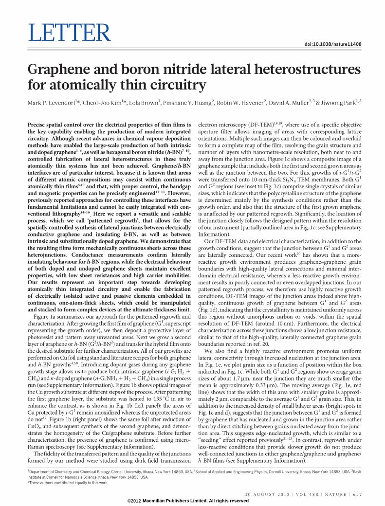
Successful synthesis of these hybrid films allows us to fabricateelectrically isolated graphene devices in a single, atomically flat sheet,which we show in Fig. 3a. We observe conducting behaviour confinedto the patterned graphene areas, with the h-BN2 showing no conduc-tivity within the limits of our equipment (sheet resistanceRsheet . 400 TV%
21, where % indicates a square of the materialhaving no thickness). We also confirm that our h-BN is free of small
PL/RIE
First growthFirst growth
Regrow
a Second growthSecond growth
2 μm
1 μm
i-G1
i-G2
0 2 4 6 8
Gra
in s
ize (μ
m)
Position, x (μm)
0.1
1.0
x= 0
50 μm
i-G1
135 °C in air
i-G1 + i-G2
i-G1
i-G2c
b
d
e
Figure 1 | Process schematic and DF-TEM characterization of grapheneheterostructures. a, Schematic for formation of atomically thin lateralheterojunctions using photolithography (PL) and reactive ion etching (RIE).See main text for details. b, The left panel shows an optical image of a patternedCu/G1 foil oxidized to enhance contrast (the dark areas are Cu). The right panelshows an optical image after reduction of CuOx and subsequent growth of
intrinsic-G2 (i-G2). c, False-colour DF-TEM image of an i-G1/i-G2 patternedarea (schematic in inset). d, Zoomed-in image of the junction region. e, Plot ofgrain size versus position in the box outlined in c. Dotted lines indicate averagegrain size away from (blue line) and near (highlighted region and orange line)the junction. Shading indicates the width of the region with smaller grains.
RESEARCH LETTER
6 2 8 | N A T U R E | V O L 4 8 8 | 3 0 A U G U S T 2 0 1 2
Macmillan Publishers Limited. All rights reserved©2012

conducting pockets of h-BNC (boron-nitride-carbon) that might formduring growth10 using electrostatic force microscopy (EFM)(Supplementary Information and Fig. 3c, right). The EFM phase shiftis highly uniform within both the i-G1 and h-BN2 regions; however,there is an abrupt change in the phase shift at the junction betweeni-G1 and h-BN2 owing to the different electrical conductivities of thesematerials, indicating very little carbon contamination bleeding into theh-BN2 region.
These sheets are particularly useful for ultraflat three-dimensionalelectronics24, where alternating h-BN and graphene regions can act as awire array connected by lateral insulators. Because such an array main-tains a uniform thickness throughout, the device will remain flat evenafter multiple transfers of such sheets without any post-processing,such as chemical mechanical polishing. We demonstrate this inFig. 3b and c, where we fabricated a large sheet of i-G1/h-BN2 linesand performed multiple transfers onto a single substrate. After trans-ferring the first sheet, a second was placed perpendicular to the first,with each layer contacted by electrodes. Optical images (Fig. 3b) showthe structural uniformity of the final devices at different scales. Theflatness and electrical properties of one such graphene–graphenecrossed junction (inset in Fig. 3b,) is studied by atomic force micro-scopy (AFM) height (Fig. 3c, left panel) and EFM phase (Fig. 3c, rightpanel) measurements. Topographically, region A (h-BN on h-BN) isalmost indistinguishable from region B (h-BN on graphene), as shownby the height histograms from each region. This contrasts with the
EFM phase image, where both the bottom and top graphene strips aredetected with nearly identical phase shifts. The small differencebetween the EFM phases of the two areas nevertheless indicates thatthe h-BN on top of the bottom graphene strip is acting as a dielectricfilm (see Supplementary Information). Electrical measurements(Fig. 3c, right panel) of these connections show a negligible additionof a contact resistance, confirming that such films behave as atomicallyflat three-dimensional interconnects. Although the vertical tunnellingcurrent through one layer of h-BN is significant25,26, few-layer h-BNformed by additional transfers could be used to electrically isolatedevices vertically as well, and allow fabrication of other passiveelements, such as capacitors27.
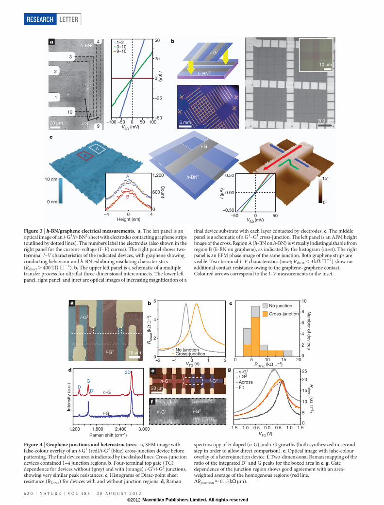
Unlike G/h-BN structures, however, electrically conductive hetero-junctions require characterization and optimization of the junctionresistance. For this purpose, we fabricated arrays of devices that con-tained zero to four i-G1/i-G2 junctions. A false-colour SEM of anexample cross-junction device is shown in Fig. 4a. The sheet resistanceat the Dirac point (RDirac) for each device was measured using top-gated four-terminal measurements (Fig. 4b) and compiled for statist-ical comparison (Fig. 4c). Devices with (orange; 15 devices) andwithout (grey; 19 devices) junctions show both narrow distributionsof RDirac, as well as similar medians (no junction: 6.6 kV%
21; cross-junction: 6.9 kV%
21). This shows that the electrical properties ofheterojunction devices are similar to that of devices without junctions,despite the presence of many smaller grains in the junction area
50 μm
d
250 nm
i-G1
i-G1
h-BN2
h-BN2
a
500 nm
1,325
1,369
1,375 1,425
Inte
nsity (a.u
.)
Raman shift (cm–1)
c
f
188 190 192 194300
400
500
600
Inte
nsity (c.p
.s.)
B 1s
h-BN peak
396 398 400 402300
600
900
1,200
1,500N 1sDataFit
DataFit
Binding energy (eV)
~30 nm
SiO2 e–
10 μm
2D band b
5 μm
SEM
h-BN2
i-G1
5 nm
0
1
0 10 20 30 40 50
Position (nm)
Inte
nsity
(a.u
.)
g
e
h-BN
Figure 2 | h-BN/G heterostructure synthesis and structuralcharacterization. a, False-colour DF-TEM image of an h-BN sheet grown in anenvironment of low reactivity with domains .1mm. Arrows indicate regionswhere the h-BN film failed to connect. Inset, representative diffraction imagetaken from the h-BN sheet, indicating hexagonal crystal structure. b, Opticalimage of an i-G1 (darker areas)/h-BN2 (lighter areas) on a Si/SiO2 substrate.Inset, Raman graphene 2D band (area indicated by the dotted box) showing astark contrast between the regions. c, X-ray photoelectron spectroscopy data(upper panels, the transition from the 1s orbital) for an i-G1/h-BN2 sheet(h-BN2 grown in a more reactive environment than a), showing a 1:1.08 B:N
atomic ratio. Raman spectroscopy (lower panel) confirms the presence of theh-BN peak. d, False-colour DF-TEM image of a suspended i-G1/h-BN2 sheetwith the junction region clearly starting at the sharp line that ends the i-G1 area.e, SEM image of i-G1/h-BN2 film suspended over 2-mm-sized holes. Highercontrast (left panel) highlights i-G1/h-BN2 regions, whereas lower contrast(right panel) shows the suspended film. f, Schematic for cross-sectional STEMEELS. g, The upper panel shows the elemental map of an i-G1/h-BN2 junctionregion containing graphitic carbon (red; g-C), boron (green), and oxygen(blue). The lower panel shows the intensity profile of g-C and boron, indicatingno voids or overlap in the junction region.
LETTER RESEARCH
3 0 A U G U S T 2 0 1 2 | V O L 4 8 8 | N A T U R E | 6 2 9
Macmillan Publishers Limited. All rights reserved©2012
0 nm
10 nm
b
c
20 μm
I (nA
)
1
2
3
4
9
10
VSD (mV)
1–23–109–10
–100 –50 0 50 100–50
–25
0
25
50a
200 μm
10 μm
i-G1
i-G1
i-G1
h-BN2
h-BN2
h-BN2
0°
15°
–50 0 50–0.50
0.00
0.50
I (μA
)VSD (mV)
–4 0 40
600
1,200
Co
unt
Height (nm)
A
A
B
B
5 mm
h--BNN2
iiii-G-G1ii G1G1
h-BN2
i-G1
i-G1
h-BN2
Figure 3 | h-BN/graphene electrical measurements. a, The left panel is anoptical image of an i-G1/h-BN2 sheet with electrodes contacting graphene strips(outlined by dotted lines). The numbers label the electrodes (also shown in theright panel for the current–voltage (I–V) curves). The right panel shows two-terminal I–V characteristics of the indicated devices, with graphene showingconducting behaviour and h-BN exhibiting insulating characteristics(Rsheet . 400 TV%
21). b, The upper left panel is a schematic of a multipletransfer process for ultraflat three-dimensional interconnects. The lower leftpanel, right panel, and inset are optical images of increasing magnification of a
final device substrate with each layer contacted by electrodes. c, The middlepanel is a schematic of a G1–G1 cross-junction. The left panel is an AFM heightimage of the cross. Region A (h-BN on h-BN) is virtually indistinguishable fromregion B (h-BN on graphene), as indicated by the histogram (inset). The rightpanel is an EFM phase image of the same junction. Both graphene strips arevisible. Two-terminal I–V characteristics (inset; Rsheet , 3 kV%
21) show noadditional contact resistance owing to the graphene–graphene contact.Coloured arrows correspond to the I–V measurements in the inset.
Num
ber o
f devic
es
RDirac (kΩ –1)0 5 10 15 20
0
2
4
6
8
10
10 μmi-G1
i-G2
Fit
n-G1
i-G2
Across
–1.5 –1.0 –0.5 0.0 0.5 1.0 1.50
5
10
15
20
25
Rsh
eet (kΩ
–1)
Rsh
eet (kΩ
–1
)
VTG (V)
g
i-G
n-G
G
DD′
2D
1,200 1,800 2,400 3,000
Inte
nsity (a.u
.)
Raman shift (cm–1)
cb
d
i-G2
20 μm
n-G1
e
i-G2n-G1
f
a
Cross-junction
No junction
0
2
4
6
VTG (V)–2 –1 0 1 2
Cross-junctionNo junction
Figure 4 | Graphene junctions and heterostructures. a, SEM image withfalse-colour overlay of an i-G1 (red)/i-G2 (blue) cross-junction device beforepatterning. The final device area is indicated by the dashed lines. Cross-junctiondevices contained 1–4 junction regions. b, Four-terminal top gate (TG)dependence for devices without (grey) and with (orange) i-G1/i-G2 junctions,showing very similar peak resistances. c, Histograms of Dirac-point sheetresistance (RDirac) for devices with and without junction regions. d, Raman
spectroscopy of n-doped (n-G) and i-G growths (both synthesized in secondstep in order to allow direct comparison). e, Optical image with false-colouroverlay of a heterojunction device. f, Two-dimensional Raman mapping of theratio of the integrated D9 and G peaks for the boxed area in e. g, Gatedependence of the junction region shows good agreement with an area-weighted average of the homogenous regions (red line,DRjunction < 0.15 kVmm).
RESEARCH LETTER
6 3 0 | N A T U R E | V O L 4 8 8 | 3 0 A U G U S T 2 0 1 2
Macmillan Publishers Limited. All rights reserved©2012
(Fig. 1). Additionally, field-effect carrier mobilities near the Diracpoint remain high (.10,000 cm2 V21 s21) for both types of devices,which is consistent with the properties of electrically transparent,laterally connected grain boundaries grown under reactive growthconditions20
.
Our method thus allows for the growth of doped heterostructures,such as p–n junctions, within a single sheet of graphene, which couldenable the production of active components with mechanically andelectrically continuous junctions. Figure 4e shows a false-colouroptical image of a device with two differently doped graphene areas(n-G1/i-G2). The n-doped graphene area exhibits an additional D9
peak (due to the presence of substitutional nitrogen dopants; Fig. 4d,red curve) that is not typically seen in i-G growths (blue curve).The location of the junction region was thus confirmed using two-dimensional Raman mapping of the ratio of the integrated D9 and Gpeaks (Fig. 4f), where the n-G1 region is much brighter5. Electricalmeasurements within and across these regions again confirm electricalcontinuity across this region. Using top gates (5 nm Cr/45 nm Au,100 nm of evaporated SiO2) we measured the gate dependence indifferent regions, as shown in Fig. 4g (n-G1/i-G2). The device showsbehaviour consistent with high-quality graphene, even across the junc-tion region. The gate dependence of Rsheet in this area is in excellentagreement with an area-weighted average of the n-G1 and i-G2 areaswith the addition of the small resistanceDRjunction < 0.15 kVmm (con-sistent with the small junction resistance seen in Fig. 4c).
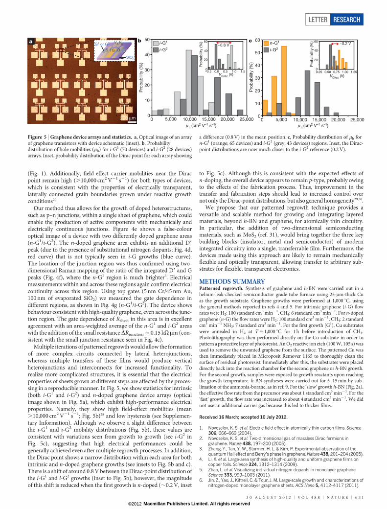
Multiple iterations of patterned regrowth would allow the formationof more complex circuits connected by lateral heterojunctions,whereas multiple transfers of these films would produce verticalheterojunctions and interconnects for increased functionality. Torealize more complicated structures, it is essential that the electricalproperties of sheets grown at different steps are affected by the proces-sing in a reproducible manner. In Fig. 5, we show statistics for intrinsic(both i-G1 and i-G2) and n-doped graphene device arrays (opticalimage shown in Fig. 5a), which exhibit high-performance electricalproperties. Namely, they show high field-effect mobilities (mean.10,000 cm2 V21 s21; Fig. 5b)28 and low hysteresis (see Supplemen-tary Information). Although we observe a slight difference betweenthe i-G1 and i-G2 mobility distributions (Fig. 5b), these values areconsistent with variations seen from growth to growth (see i-G2 inFig. 5c), suggesting that high electrical performances could begenerally achieved even after multiple regrowth processes. In addition,the Dirac point shows a narrow distribution within each area for bothintrinsic and n-doped graphene growths (see insets to Fig. 5b and c).There is a shift of around 0.8 V between the Dirac-point distribution ofthe i-G1 and i-G2 growths (inset to Fig. 5b); however, the magnitudeof this shift is reduced when the first growth is n-doped (,0.2 V, inset
to Fig. 5c). Although this is consistent with the expected effects ofn-doping, the overall device appears to remain p-type, probably owingto the effects of the fabrication process. Thus, improvement in thetransfer and fabrication steps should lead to increased control overnot only the Dirac-point distributions, but also general homogeneity29,30.
We propose that our patterned regrowth technique provides aversatile and scalable method for growing and integrating layeredmaterials, beyond h-BN and graphene, for atomically thin circuitry.In particular, the addition of two-dimensional semiconductingmaterials, such as MoS2 (ref. 31), would bring together the three keybuilding blocks (insulator, metal and semiconductor) of modernintegrated circuitry into a single, transferrable film. Furthermore, thedevices made using this approach are likely to remain mechanicallyflexible and optically transparent, allowing transfer to arbitrary sub-strates for flexible, transparent electronics.
METHODS SUMMARYPatterned regrowth. Synthesis of graphene and h-BN were carried out in ahelium-leak-checked semiconductor grade tube furnace using 25-mm-thick Cuas the growth substrate. Graphene growths were performed at 1,000 uC, usingthe general methods reported in refs 4 and 5. For intrinsic graphene (i-G) flowrates were H2: 100 standard cm3 min21, CH4: 6 standard cm3 min21. For n-dopedgraphene (n-G) the flow rates were H2: 100 standard cm3 min21, CH4: 2 standardcm3 min21 NH3: 7 standard cm3 min21. For the first growth (G1), Cu substrateswere annealed in H2 at T 5 1,000 uC for 1 h before introduction of CH4.Photolithography was then performed directly on the Cu substrate in order topattern a protective layer of photoresist. An O2 reactive ion etch (100 W, 105 s) wasused to remove the unwanted graphene from the surface. The patterned Cu wasthen immediately placed in Microposit Remover 1165 to thoroughly clean thesurface of residual photoresist. Immediately after this, the substrates were placeddirectly back into the reaction chamber for the second graphene or h-BN growth.For the second growth, samples were exposed to growth reactants upon reachingthe growth temperature. h-BN syntheses were carried out for 5–15 min by sub-limation of the ammonia-borane, as in ref. 9. For the ‘slow’ growth h-BN (Fig. 2a),the effective flow rate from the precursor was about 1 standard cm3 min21. For the‘fast’ growth, the flow rate was increased to about 4 standard cm3 min21. We didnot use an additional carrier gas because this led to thicker films.
Received 16 March; accepted 10 July 2012.
1. Novoselov, K. S. et al. Electric field effect in atomically thin carbon films. Science306, 666–669 (2004).
2. Novoselov, K. S. et al. Two-dimensional gas of massless Dirac fermions ingraphene. Nature 438, 197–200 (2005).
3. Zhang, Y., Tan, Y.-W., Stormer, H. L. & Kim, P. Experimental observation of thequantum Hall effect and Berry’s phase in graphene. Nature 438, 201–204 (2005).
4. Li, X. et al. Large-area synthesis of high-quality and uniform graphene films oncopper foils. Science 324, 1312–1314 (2009).
5. Zhao, L. et al. Visualizing individual nitrogen dopants in monolayer graphene.Science 333, 999–1003 (2011).
6. Jin, Z., Yao, J., Kittrell, C. & Tour, J. M. Large-scale growth and characterizations ofnitrogen-doped monolayer graphene sheets. ACS Nano 5, 4112–4117 (2011).
200 μm
n-G1
i-G2
0 5,000 10,000 15,000 20,000 25,0000
10
20
30
40
50
Pro
bab
ility
(%
)
Pro
bab
ility
(%
)
μh (cm2 V–1 s–1)
0 5,000 10,000 15,000 20,000 25,000
μh (cm2 V–1 s–1)
i-G1
i-G2
–0.5 0.0 0.5 1.0 1.50
20
40
60
Pro
bab
ility
(%
)
VDirac (V)
Pro
bab
ility
(%
)
VDirac (V)
b c
0
10
20
30
40
50
60
0.25 0.50 0.75 1.00 1.250
20
40
60~0.2 V~0.8 VG1 or G2
SiO2
TGS D
VAVBa
Figure 5 | Graphene device arrays and statistics. a, Optical image of an arrayof graphene transistors with device schematic (inset). b, Probabilitydistribution of hole mobilities (mh) for i-G1 (70 devices) and i-G2 (28 devices)arrays. Inset, probability distribution of the Dirac point for each array showing
a difference (0.8 V) in the mean position. c, Probability distribution of mh forn-G1 (orange; 65 devices) and i-G2 (grey; 43 devices) regions. Inset, the Dirac-point distributions are now much closer to the i-G2 reference (0.2 V).
LETTER RESEARCH
3 0 A U G U S T 2 0 1 2 | V O L 4 8 8 | N A T U R E | 6 3 1
Macmillan Publishers Limited. All rights reserved©2012

7. Kubota, Y., Watanabe, K., Tsuda, O. & Taniguchi, T. Deep ultraviolet light-emittinghexagonal boron nitride synthesized at atmospheric pressure. Science 317,932–934 (2007).
8. Kim, K. K. et al. Synthesis of monolayer hexagonal boron nitride on Cu foil usingchemical vapor deposition. Nano Lett. 12, 161–166 (2012).
9. Song, L. et al. Large scale growth and characterization of atomic hexagonal boronnitride layers. Nano Lett. 10, 3209–3215 (2010).
10. Ci, L.et al. Atomic layers of hybridized boron nitrideandgraphenedomains. NatureMater. 9, 430–435 (2010).
11. Liu, Y., Bhowmick, S. & Yakobson, B. I. BN white graphene with ‘‘colorful’’ edges:the energies and morphology. Nano Lett. 11, 3113–3116 (2011).
12. Pruneda, J. M. Origin of half-semimetallicity induced at interfaces of C-BNheterostructures. Phys. Rev. B 81, 161409 (2010).
13. Miyamoto, Y., Rubio, A., Cohen, M. & Louie, S. Chiral tubules of hexagonal BC2N.Phys. Rev. B 50, 4976–4979 (1994).
14. Wehling, T. O. et al. Molecular doping of graphene. Nano Lett. 8, 173–177 (2008).15. Williams, J. R., Dicarlo, L. & Marcus, C. M. Quantum Hall effect in a gate-controlled
p-n junction of graphene. Science 317, 638–641 (2007).16. Dresselhaus, M. S., Jorio, A., Hofmann, M., Dresselhaus, G. & Saito, R. Perspectives
on carbon nanotubes and graphene Raman spectroscopy. Nano Lett. 10,751–758 (2010).
17. Chen, S. et al. Oxidation resistance of graphene-coated Cu and Cu/Ni alloy. ACSNano 5, 1321–1327 (2011).
18. Huang, P. Y. et al. Grains and grain boundaries in single-layer graphene atomicpatchwork quilts. Nature 469, 389–392 (2011).
19. Kim, K. et al. Grain boundary mapping in polycrystalline graphene. ACS Nano 5,2142–2146 (2011).
20. Tsen, A. W. et al. Tailoring electrical transport across grain boundaries inpolycrystalline graphene. Science 336, 1143–1146 (2012).
21. Yu, Q. et al. Control and characterization of individual grains and grain boundariesin graphene grown by chemical vapour deposition. Nature Mater. 10, 443–449(2011).
22. Sun, Z. et al. Growth of graphene from solid carbon sources. Nature 468, 549–552(2010).
23. Kim, Y.-J., Lee, J.-H. & Yi, G.-C. Vertically aligned ZnO nanostructures grown ongraphene layers. Appl. Phys. Lett. 95, 213101 (2009).
24. Dean, C. R. et al. Boron nitride substrates for high-quality graphene electronics.Nature Nanotechnol. 5, 722–726 (2010).
25. Britnell, L. et al. Electron tunneling through ultrathin boron nitride crystallinebarriers. Nano Lett. 12, 1707–1710 (2012).
26. Lee, G.-H. et al. Electron tunneling through atomically flat and ultrathin hexagonalboron nitride. Appl. Phys. Lett. 99, 243114 (2011).
27. Sanchez-Yamagishi, J. et al. Quantum Hall effect, screening, and layer-polarizedinsulating states in twisted bilayer graphene. Phys. Rev. Lett. 108, 076601 (2012).
28. Meric, I. et al. Current saturation in zero-bandgap, top-gated graphene field-effecttransistors. Nature Nanotechnol. 3, 654–659 (2008).
29. Moser, J., Barreiro, A. & Bachtold, A. Current-induced cleaning of graphene. Appl.Phys. Lett. 91, 163513 (2007).
30. Liang, X. et al. Toward clean and crackless transfer of graphene. ACS Nano 5,9144–9153 (2011).
31. Radisavljevic, B., Radenovic, A., Brivio, J., Giacometti, V. & Kis, A. Single-layer MoS2transistors. Nature Nanotechnol. 6, 147–150 (2011).
Supplementary Information is available in the online version of the paper.
Acknowledgements We thank P. McEuen and M. Spencer for discussions. This workwasmainly supportedbyAFOSR grants (FA9550-09-1-0691andFA9550-10-1-0410)and the NSF through the Cornell Centers for Materials Research (NSF DMR-1120296),which also provided the electronmicroscopy facilities. Additional funding was providedby the Alfred P. Sloan Foundation. L.B. was partially supported by a Fullbrightscholarship; R.W.H. and P.Y.H. were supported by an NSF Graduate ResearchFellowship. Device fabrication was performed at the Cornell NanoScale Facility, amember of the National Nanotechnology Infrastructure Network, which is supportedby the National Science Foundation (grant ECS-0335765).
Author Contributions M.P.L. and C.-J.K. contributed equally to this work. Synthesis,device fabrication, and electrical measurements and analysis were done by M.P.L. andC.-J.K. DF-TEM and data analysis were performed by L.B. and C.-J.K. EELSmeasurement and data analysis were conducted by P.Y.H. and D.A.M. Ramanmeasurements and analysis were carried out by M.P.L. with assistance from R.W.H. J.P.designed the experiments and oversaw the research. M.P.L. and J.P. wrote themanuscript with assistance from R.W.H and input from all authors.
Author Information Reprints and permissions information is available atwww.nature.com/reprints. The authors declare competing financial interests: detailsare available in the online version of the paper. Readers are welcome to comment onthe online version of the paper. Correspondence and requests for materials should beaddressed to J.P. ([email protected]).
RESEARCH LETTER
6 3 2 | N A T U R E | V O L 4 8 8 | 3 0 A U G U S T 2 0 1 2
Macmillan Publishers Limited. All rights reserved©2012