“metallic” boron nitride -...
TRANSCRIPT

„Metallic’” boron nitride Section E-Research paper
Eur. Chem. Bull., 2015, 4(1), 8-23 8
“METALLIC” BORON NITRIDE
R. Becker,[a] L. Chkhartishvili,[b,c]* R. Avci,[d] I. Murusidze,[e] O. Tsagareishvili[c] and N. Maisuradze[b]
Presented at 3rd International Conference “Nanotechnologies”, October 20 – 24, 2014, Tbilisi, Georgia
(Nano – 2014)
Keywords: boron nitride, non-stoichiometric chemical composition, metallization by doping.
Boron nitride shell structures of chemical composition BNx with boron excess (x << 1) contaminated with carbon are synthesized in theprocess of melting of a boron-rich material in a boron nitride crucible with the nitrogen source in the form of high-purity pressed boronnitride rods, which held up the crucible. The obtained material is found to be conductive despite the fact that all the boron nitrides ofstoichiometric chemical composition BN are insulators. “Metallic” boron nitride is modelled as a mixture of structural modifications ofsemiconducting boron and boron carbide heavily doped with nitrogen. First principle calculations performed within the quasi-classicalapproximation prove that nitrogen impurities, accommodated in large crystallographic voids characteristic of all-boron and boron-richcrystalline lattices, create donor electron-states inside the conduction band and then lead to the local “metallization” of chemical bonds inthese initially covalently bonded structures. * Corresponding Author
E-Mail: [email protected] [a] Boron Cluster Metamaterials, Cluster Sciences Research
Institute, 39 Topsfield Rd., Ipswich, MA 01938, USA, [email protected], [email protected]
[b] Department of Engineering Physics, Georgian Technical University, 77 M. Kostava Ave., Tbilisi 0175, Georgia, [email protected], [email protected]
[c] Laboratory for Boron & Powdered Composite Materials, F. Tavadze Institute of Metallurgy & Materials Science, 15 A. Kazbegi Ave., Tbilisi 0160, Georgia, [email protected], [email protected]
[d] Department of Physics, Montana State University, Bozeman, MT 59717, USA, [email protected]
[e] Institute of Applied Physics, Ilia State University, 3/5 K. Cholokashvili Ave., Tbilisi 0162, Georgia, [email protected]
Introduction
Boron nitrides with the chemical formula BN, i.e. stoichiometric ratio of B : N = 1 : 1, can exist in various forms: diatomic molecule, plane fragments of a hexagonal sheet, nanotubes, fullerenes, hexagonal (h-BN), rhombohedral (r-BN), cubic (c-BN) and wurtzite-like (w-BN) crystals. It is well proved both experimentally and theoretically that all of them possess wide band or HOMO – LUMO gaps. Their chemical-bonding and electronic properties are well-studied. In particular, we have theoretically studied electronic structure of the BN diatomic molecule,1 BN infinite hexagonal sheet,2 and h-BN,3 c-BN4 and w-BN crystals5 applying a quasi-classical-type method of calculation.
Boron nitride of composition BN is a chemical analogue of carbon. They are similar to each other and share similar structures of various dimensionality: hexagonal sheets and layered crystals, nanotubes and fullerenes, zinc blende and wutzite-like crystals. However, unlike carbon which can be metallic, BN is an insulator irrespective of its structure and dimensionality. Namely, 3D boron nitrides are known as wide band gap insulators what limits their application in electronics.
However, if some process (e.g. doping) could induce metallicity in these structures, then 3D BN would turn into a novel material with a potential for applications in electronics beyond conventional ceramics.
The possibilities of the intrinsic metallicity of BN were discussed in a few papers.
The high pressure room temperature phase transition in BN from the diamond-like insulating structure into the white-tin-like metallic structure was calculated for the first time in reference.6 As for the recent calculations, it should be mentioned the density-functional-theory (DFT) study,7 which has predicted that c-BN (111) nanofilms are metallic and turn into semiconductors once their thickness is too small. Note that such exceptional metallic behavior is not truly intrinsic, but due to a combined effect of thickness-dependent inbuilt electric polarization and labile near-gap states unique to polar nanofilms. On the basis of theoretical calculations, it has been proposed a dynamically stable tetragonal phase of BN which is metallic.8 The analysis of its band structure, density of states, and electron localization function confirms the origin of the metallic behaviour to be due to the delocalized B 2p electrons.
By the DFT a series of 1D NFE (nearly-free-electron) bands of BN nanotubes with on-axis spatial distributions was also found.9 These nanotubular states originate from the screening responsible for the image potential of the parent 2D BN sheets. When the nanotube radius exceeds the radial extent of NFE states, their energies converge to those of image potential states. The comparative DFT analysis in generalized-gradient-approximation (GGA) performed on electronic properties of BN single-walled zigzag nanotubes, as well as their BP and BAs analogues confirms10 that, all these BN nanotubes are semiconducting in nature, whereas BP and BAs nanotubes are metallic up to some diameter. A superconductivity state was predicted11 by Green’s function approach in a zigzag BN nanotube within the extended attractive Hubbard model.

„Metallic’” boron nitride Section E-Research paper
Eur. Chem. Bull., 2015, 4(1), 8-23 9
However, in most cases the metallicity of boron nitrides with the stoichiometric ratios of B : N ≈ 1 : 1 must be related to point, dot-like or linear structural defects.
The DFT employing the local-spin-density-approximation (LSDA) was used12 to show that increasing of the B-content relative to the N-content in BN nanoribbons, which are insulators, can significantly reduce the band gap making them semiconducting. In particular, armchair ribbons having excess of B-atoms were predicted to have a more stable triplet structure with a higher density-of-states (DOS) at the top of the valence band near the Fermi level. The influence of vacancies and substitutional defects on the electronic properties of h-BN in 2D molecular model was studied13 using DFT at the level of local-density-approximation (LDA) and found that these point defects reduce the HOMO – LUMO energy gap.
Triangle-shaped nanohole, nanodot, and lattice antidot structures in h-BN monolayer sheets characterized with DFT calculations utilizing the LSDA14 have revealed that N-terminated nanodots and antidots show half-metallicity. In spite of significant lattice contraction due to the presence of multiple holes, antidot superlattices were predicted to be stable, also exhibiting enhanced half-metallicity.
The synthesis of highly porous BN nanospheres with a rough surface consisting of open nanocones and corrugated ribbons has been described.15 They exhibited surprisingly stable field emission properties at low turn-on voltages. These electron emission properties must be attributed to the presence of finite BN ribbons with zigzag edges which behave like metals as confirmed by first-principles calculations. They indicated that the work function associated to zigzag BN ribbons is lower when compared with BN-bulk material. Authors claimed that it was for the first time the possibility of finding a sort of metallic BN was reported. The theoretical evidence based on total-energy first-principles calculations of the existence of states and extended along the edges of bare zigzag BN-nanoribbons has been presented as well.16 In particular, it was shown that there was a rich spectrum of electronic behaviors which could be controlled by applying an external electric field in order to obtain metallic ↔ semiconducting ↔ half-metallic transitions. The electronic structure calculations for the zigzag-edged BN nanoribbons by using DFT showed17 that the ground states of the ribbons with an N-edge are half-metallic. According to the first-principles spin-polarized calculations,18 the BN nanoribbons with topological line defects exhibit diverse electronic properties, including half-metallicity and half-semimetallicity, depending on the type of edge and line defect. Furthermore, an applied tensile strain can tune the half-semimetal gap. The comprehensive study19 of the effects of line defects on electronic properties of monolayer BN sheets, nanoribbons, and single-walled nanotubes using first-principles calculations and Born–Oppenheimer quantum molecular dynamic (MD) simulation shows that although line defects divide the BN sheet (or nanotube) into domains they can lead to edges that significantly reduce the band gap. In particular, the line-defect-embedded zigzag BN nanoribbons with only N-terminated edges are predicted to be metallic at the ground state. The BN stereo-nanoribbons constructed by three BN ribbon wings connected via the junctions were investigated using first-principles calculations.20 It was found that for the zigzag edges, the tri-wing BN nanoribbons can be metals or
narrow-band gap semiconductors depending on the bonding characteristics; the sp3-bonding junctions even induce the metallic behaviors. However, it was also demonstrated,21 using a combination of transmission-electron-microscopy (TEM) data and DFT calculations, that covalent interlayer bonds can be formed spontaneously at the edges of a h-BN bilayer resulting in subångström distortions of the atomic structure of the edge, and reconstruction of this closed edge can help the material to recover its bulk-like insulating behavior and thus disprove the predicted metallic character of open edges.
The metallicity of boron nitrides with the stoichiometric ratio of B : N ≈ 1 : 1 also can be related to the impurities.
The first-principles investigation22 of the electronic properties of BN nanoribbons having edges passivated by H-atoms showed that band gap for nanoribbons with armchair-shaped edges exhibited oscillations as their width increases. For the wider ribbons it converges to the constant value of 0.02 eV, while for nanoribbons with zigzag edges the band gap monotonically decreased and converged to the gap of 0.70 eV. Both these values are significantly smaller than the bulk gap due to the presence of the edge-states. Calculations of the electronic structure of H-terminated zigzag B-edged BN nanoribbons by using DFT even showed that their ground states are half-metallic. The intriguing electronic properties of fully and partially hydrogenated BN nanoribbons were investigated by means of first-principles computations.23 Irrespective of ribbon width, fully hydrogenated zigzag BN nanoribbons were found to be metallic. The partially hydrogenated zigzag BN nanoribbons exhibit a semiconductor → half-metal → metal transition that occurs when the hydrogenated part is dominant. According to the electronic characteristics of fully hydrogenated BN layer and zigzag-edged BN nanoribbons investigated by using DFT, the zigzag-edged BN nanoribbon (prominently fabricated in experiments) possesses half-metallicity with full hydrogenation and this property can be tuned by applying a transverse electric bias.24 Few-layer rippled h-BN membranes also exhibit25 distinct and pronounced changes in their electronic properties after the atomic H-plasma treatment: the band gap reduced, which is a signature of transition from the insulating to the semiconducting regime.
By the DFT-based quantum mechanical description of the electronic properties of armchair BN nanoribbons edge-terminated with hydroxyl OH-groups or O-atoms, a reduction of band gap was observed.26 On the other hand, standard spin-polarized DFT calculations27,28 showed that unlike the semiconducting H-terminated zigzag BN nanoribbons, the O-terminated ones have two energetically degenerate ground states on the B-edge, both of which are metallic, and all the S-terminated zigzag BN nanoribbons also are metallic. The first-principles calculations29 have revealed that an oxidized hexagonal monolayer of BN supported by a Cu substrate exhibits metallic properties when O adatom vertically bonds with the B atom. This is mainly due to the hybridization of the p orbital of the BN layer and O adatom around the Fermi level. Charge transfer from the Cu substrate to the O atom stabilizes the formation of the vertical O – B bond. Injecting negative charges could trigger the migration of the O adatom from the B – N bond to B atom for supported monolayer, which will lead to a metallic transition in the oxidized nanosheet.

„Metallic’” boron nitride Section E-Research paper
Eur. Chem. Bull., 2015, 4(1), 8-23 10
DFT was utilized30 to study the electronic properties BN sheets, taking into account the presence of defects. The structure considered consisted of a central hexagon surrounded by 3 alternating pentagons and 3 heptagons. To explore the effects of doping, B and N atoms were replaced with C atoms. When a B atom was replaced with a C atom, the new structure was a semimetal. Replacing two B atoms with two C atoms also yielded a semimetal. When three B or N atoms of the central hexagon were replaced with three C atoms, the new structure exhibited transition to a conductor, which however remained a semiconductor. Results of the study31 on the effects of C-impurity doping on the DOS of the h-BN sheet within the random tight-binding model and Green’s function technique also show that doping by C reduces the band gap of the BN system and, in high concentration of C-atoms, the DOS of BN plane becomes similar to that of graphene sheet, resulting in semimetallic behavior. Using DFT, as well as the Green’s function quasi-particle approach, it was studied32 the electronic structure of h-BN sheets doped with carbon and given the qualitatively correct picture of the substitutional impurity states in the gap.
The electronic structures and transport properties of fluorinated zigzag-edged BN nanoribbons were investigated by applying Green’s function and DFT.33 Results showed that the transition between half-metal and semiconductor can be realized by fluorination at different sites or by the change of the fluorination level. A comprehensive study34 on the semi-fluorinated BN bilayers was presented using DFT calculations. Due to the combined effect of intrinsic intralayer strain and interlayer charge transfer, the ferromagnetic coupling is favored, which has to exhibit half-metallic behavior for BN bilayers. However, the h-BN nanosheets actually doped with F-atoms35 via a facile chemical solution method with fluoboric acid, demonstrated a typical semiconductor characteristic.
By an investigation36 of the electronic structure of alkali-doped BN nanotubes using DFT calculations, it was found that the NFE state couples with the alkali atom states, giving rise to metallic states near the Fermi level. Not only the s- but the d-orbital states substantially take part in the hybridization, and the resulting metallic states preserve the free-electron-like energy dispersion. The nodeless wave function at the Fermi level, together with the lowered work function, constitutes the major feature of the alkali-doped BN nanotubes. The electronic and structural properties of nanotubes composed of an iron oxide FeO monolayer and BN nanotubes were investigated37 by means of a GGA implementation of DFT. Depending on the diameter of the tube, they can be semiconductors, half-metals or half- semimetals that can become half-metals if charged with either electrons or holes.
And finally, the metallicity of boron nitrides with the stoichiometric ratio of B : N ≈ 1 : 1 can be related to the phase-inclusions of carbon.
According to the first-principles total-energy electronic-structure calculations performed within the LSDA38 for hexagonally bonded honeycomb ribbons consisting of B, N, and C atoms, there are metallic BNC ribbons with different zigzag edges, C and BN or NB. The first-principles study39 also suggested that hybrid C/BN nanoribbons with dihydrogenated edges can possess half-metallicity with a certain range of widths for the graphene and BN sections.
The hybrid C/BN nanoribbons can undergo the semiconductor-to-half-metal-to-metal transitions as the width of both graphene and BN nanoribbons increases. In particular, the dihydrogenation of the B-edge can induce localized edge states around the Fermi level, and the interaction among them can lead to the semiconductor-to-half-metal-to-metal transitions. The transport properties of hybrid nanoribbons formed by partially substituting zigzag BN (or graphene) nanoribbons into zigzag graphene (or BN) nanoribbons have been investigated using the first-principles nonequilibrium Green’s function method.40 The electrical transport was found to be highly improved with the transmission conductance around the Fermi level. The enhancement in these hybrid systems was attributed to the coupling effect between B (or N) atoms and C atoms at the interfaces, which introduces a pair of bonding and antibonding bands around the Fermi level. Based on a first-principle calculations it was also reported41 the size limitation of half-metallic properties in hybrid zigzag BCN nanoribbons. Electronic properties of all hybrid systems are mainly determined by the C- rather than BN-segments. Transitions between semiconductor, half-metal and metal can be realized as the width of the carbon segment increases. Such atomic layers containing hybridized domains of graphene and h-BN, i.e. h-BNC, constitute a different type of disordered 2D electronic system. Magneto-electric transport measurements performed at low temperature in vapor phase synthesized h-BNC layers showed42 a clear and anomalous transition from an insulating to a metallic behavior upon cooling. This transition can be modulated by electron- and hole-doping and by the application of an external magnetic field. These results supported by first principles calculations suggest that this transition in h-BNC is the result of the coexistence between percolation through metallic graphene networks and hopping conduction between edge states on randomly distributed insulating h-BN domains. Novel electronic properties of various-sized graphene nanoflakes embedded in a BN layer were also studied in ref.43 In addition, it was found44 that depending on the sizes of the h-BN triangular clusters embedded in graphene supercells and the separation region between them, the spin polarization can be induced through charge-doping. The half-metallicity is observed for certain charged states, which are otherwise metallic. In these half-metallic states, the spin density is concentrated near the edges of the clusters, in analogy to the more common predictions for h-BN/graphene intercalated nanoribbons. The first principles results of ref.45 indicated that the heterostructures formed after C-fullerene coalescence in BN-nanotubes are metallic due to a core of corrugated C-nanotube, which provides an electron transport channel.
From the above short review one can conclude that there are a number of proposed models of metallic conductivity in boron nitrides with simple atomic structures and chemical formula BN, which are related to structural defects, impurities or phase-inclusions. However, these models fail to explain metallicity in boron-rich boron nitrides with complex clustered structures which are formed at very high temperatures.
In this work, we have obtained boron nitride of composition BNx with boron excess, i.e. x << 1, which is conductive dispite the fact that all the boron nitrides of common stoichiometric composition BN are insulators. “Metallic” boron nitride is modeled as a mixture of different

„Metallic’” boron nitride Section E-Research paper
Eur. Chem. Bull., 2015, 4(1), 8-23 11
structural modifications of semiconducting boron and boron carbide, i.e., a structure constructed from icosahedral and maybe small amount of some quasi-planar boron clusters, heavily doped with nitrogen. The calculations performed within the quasi-classical approximation have proved that nitrogen impurities accommodated in large crystallographic voids characteristic for all-boron and boron-rich lattices create electron donor states inside the conduction band and then lead to the local “metallization” of bonding.
Materials and Methods
In our experiments, high-purity pressed BN rods support the pyrolytic BN crucibles filled with powdered mixture of a metal oxide and boron (Figure 1). The crystalline boron used was of 99.999 % purity with trace contaminants being limited to water vapor and atmospheric gas adsorptions. The molten material was in full contact with the crucible for several hours during each synthesis run and even a day after the power was shut off, the crucible was still too hot. The mass of resulting polycrystalline boride was always certainly smaller than that of powder in the initial room-temperature crucible and fell out merely by inverting the crucible.
Figure 1. Crucible and its support before the melting runs.
Figure 2 shows the deposits which formed during several melting runs. There we are able to identify the badly eroded rods holding up the crucible, which however was attacked in much lesser extent. It must be due to the different degrees of structural imperfections in BN materials used in rods and crucible (like the graphite: high-purity pressed graphite easily reacts, but pyrolytic graphite does not): the crucibles material has a tiling structure which gives almost nothing for B to bind to.
It is obvious that in the presence of the B-vapor overflowing the pyrolytic BN crucible during the vacuum reduction of the charge material at temperature > 2050 °C, the highest-purity pressed BN rods (used to suspend the pyrolytic BN crucible in the optimum thermal position in the carbon-vacuum-furnace) is aggressively attacked by B-vapor from the reduction process.
Figure 2. Deposits formed on rods and crucible during several melting runs.
As for the oxygen, it would have partially sublimated from the metal oxide at much lower temperatures and been pumped away by a turbo-molecular pump directly attached to the vacuum chamber (pumping efficiency was optimized at ~ 10–6 Torr). However, rest of oxygen can evaporate, bonded with boron clusters and, therefore, their deposit should be contaminated with some oxygen as well. In a different case, when the crucible was machined from the same high-purity pressed BN as the rods, it was attacked by the molten boride too aggressively. Thus, pyrolytic BN was the material that more effectively resisted the thermo-chemical attack at such elevated temperatures.
After many subsequent melting runs, rods and crucible were covered with a paper-thin silicon-colored deposit (Figure 3).
Figure 3. Rods and crucible entirely covered with silicon-colored deposit.
„Metallic’” boron nitride Section E-Research paper
Eur. Chem. Bull., 2015, 4(1), 8-23 12
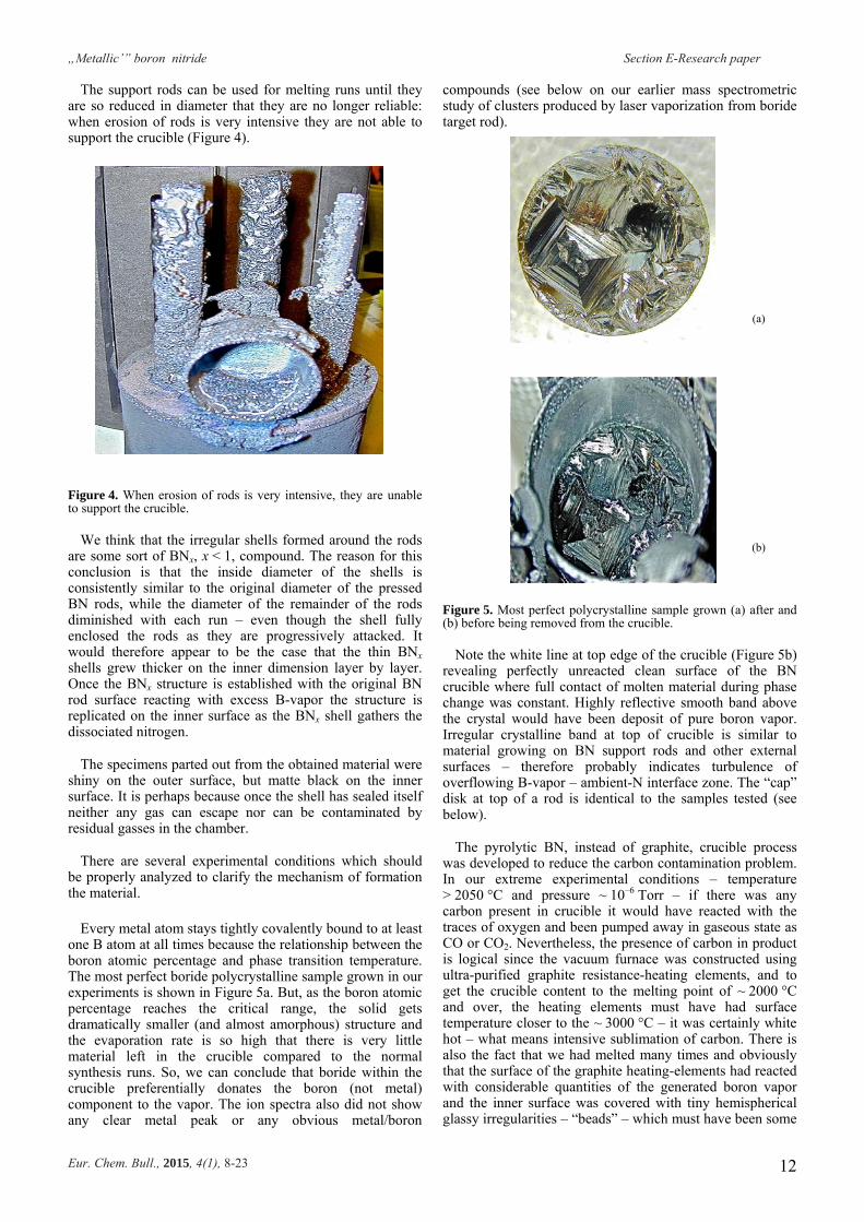
The support rods can be used for melting runs until they are so reduced in diameter that they are no longer reliable: when erosion of rods is very intensive they are not able to support the crucible (Figure 4).
Figure 4. When erosion of rods is very intensive, they are unable to support the crucible.
We think that the irregular shells formed around the rods are some sort of BNx, x < 1, compound. The reason for this conclusion is that the inside diameter of the shells is consistently similar to the original diameter of the pressed BN rods, while the diameter of the remainder of the rods diminished with each run – even though the shell fully enclosed the rods as they are progressively attacked. It would therefore appear to be the case that the thin BNx shells grew thicker on the inner dimension layer by layer. Once the BNx structure is established with the original BN rod surface reacting with excess B-vapor the structure is replicated on the inner surface as the BNx shell gathers the dissociated nitrogen.
The specimens parted out from the obtained material were shiny on the outer surface, but matte black on the inner surface. It is perhaps because once the shell has sealed itself neither any gas can escape nor can be contaminated by residual gasses in the chamber.
There are several experimental conditions which should be properly analyzed to clarify the mechanism of formation the material.
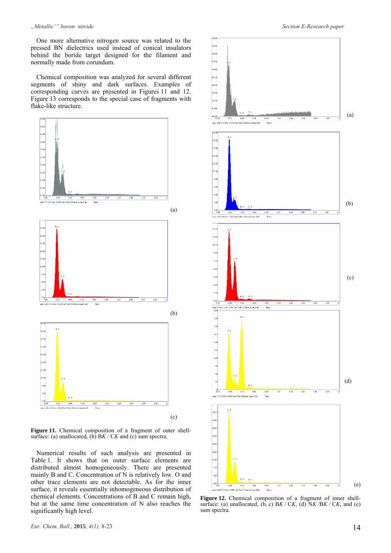
Every metal atom stays tightly covalently bound to at least one B atom at all times because the relationship between the boron atomic percentage and phase transition temperature. The most perfect boride polycrystalline sample grown in our experiments is shown in Figure 5a. But, as the boron atomic percentage reaches the critical range, the solid gets dramatically smaller (and almost amorphous) structure and the evaporation rate is so high that there is very little material left in the crucible compared to the normal synthesis runs. So, we can conclude that boride within the crucible preferentially donates the boron (not metal) component to the vapor. The ion spectra also did not show any clear metal peak or any obvious metal/boron
compounds (see below on our earlier mass spectrometric study of clusters produced by laser vaporization from boride target rod).
(a)
(b)
Figure 5. Most perfect polycrystalline sample grown (a) after and (b) before being removed from the crucible.
Note the white line at top edge of the crucible (Figure 5b) revealing perfectly unreacted clean surface of the BN crucible where full contact of molten material during phase change was constant. Highly reflective smooth band above the crystal would have been deposit of pure boron vapor. Irregular crystalline band at top of crucible is similar to material growing on BN support rods and other external surfaces – therefore probably indicates turbulence of overflowing B-vapor – ambient-N interface zone. The “cap” disk at top of a rod is identical to the samples tested (see below).
The pyrolytic BN, instead of graphite, crucible process was developed to reduce the carbon contamination problem. In our extreme experimental conditions – temperature > 2050 °C and pressure ~ 10–6 Torr – if there was any carbon present in crucible it would have reacted with the traces of oxygen and been pumped away in gaseous state as CO or CO2. Nevertheless, the presence of carbon in product is logical since the vacuum furnace was constructed using ultra-purified graphite resistance-heating elements, and to get the crucible content to the melting point of ~ 2000 °C and over, the heating elements must have had surface temperature closer to the ~ 3000 °C – it was certainly white hot – what means intensive sublimation of carbon. There is also the fact that we had melted many times and obviously that the surface of the graphite heating-elements had reacted with considerable quantities of the generated boron vapor and the inner surface was covered with tiny hemispherical glassy irregularities – “beads” – which must have been some

„Metallic’” boron nitride Section E-Research paper
Eur. Chem. Bull., 2015, 4(1), 8-23 13
sort of B/C compound and/or boron heavily doped with carbon. Such isolation should weaken this source of carbon contamination. On the other hand, there would be carbon in some form within the closed confines of the graphite fiber walls of the furnace insulation.
The reflectivity would indicate the reasonably planar polycrystalline morphology at the outer surface. This silicon-colored surface of the shell could only continue to accumulate boron due to the overflow of the B-fluid from the top of the crucible. So, it is probable that the outer surface mainly consists of condensed boron clusters. Figure 6 shows the typical microstructure of such surfaces.
Figure 6. Outer surface microstructure of a shell.
As for the inner surface, it would have grown inwards, i.e. towards the BN rod, which would be dissociating in essentially pure nitrogen and boron vapor with almost no gaseous convection effects from the chamber. However, because the rods would have some percentage of carbon contamination, and perhaps traces of oxygen and other residual gasses trapped in the pressing process, chemical composition of the product also would be more complex than simply BNx. The source of the nitrogen is without question its reduction or “gettering” from the pressed BN rods and not from the pyrolytic BN crucible because at base pressure of ~ 10–6 Torr in the chamber any external source of nitrogen would be in the ppm range and therefore not a contributing factor. The microstructure of an inner surface is shown in Figure 7. In the most part, material is built up from loosely fused droplets (Figure 8). But, there are also presented threads (Figure 9) and flakes (Figure 10).
Figure 7. Inner surface microstructure of a shell.
Figure 8. Microstructure built up from loosely fused droplets.
Figure 9. Thread presented in microstructure.
Figure 10. Flakes presented in microstructure.
Note that material with almost of similar structure can be observed in other process, when gaseous nitrogen is used, instead of argon, e.g., during an implanter run. Namely, such deposit was obtained on the front surface of the ion source arc chamber with the boride target-crystal at the opposite end from the filament. The nitrogen reactively sputtered the surface of this crystal and formed a very dense and extremely hard black deposit on the molybdenum sidewall. Typically it result was a mixture of various nano-allotropes.
„Metallic’” boron nitride Section E-Research paper
Eur. Chem. Bull., 2015, 4(1), 8-23 14
One more alternative nitrogen source was related to the pressed BN dielectrics used instead of conical insulators behind the boride target designed for the filament and normally made from corundum.
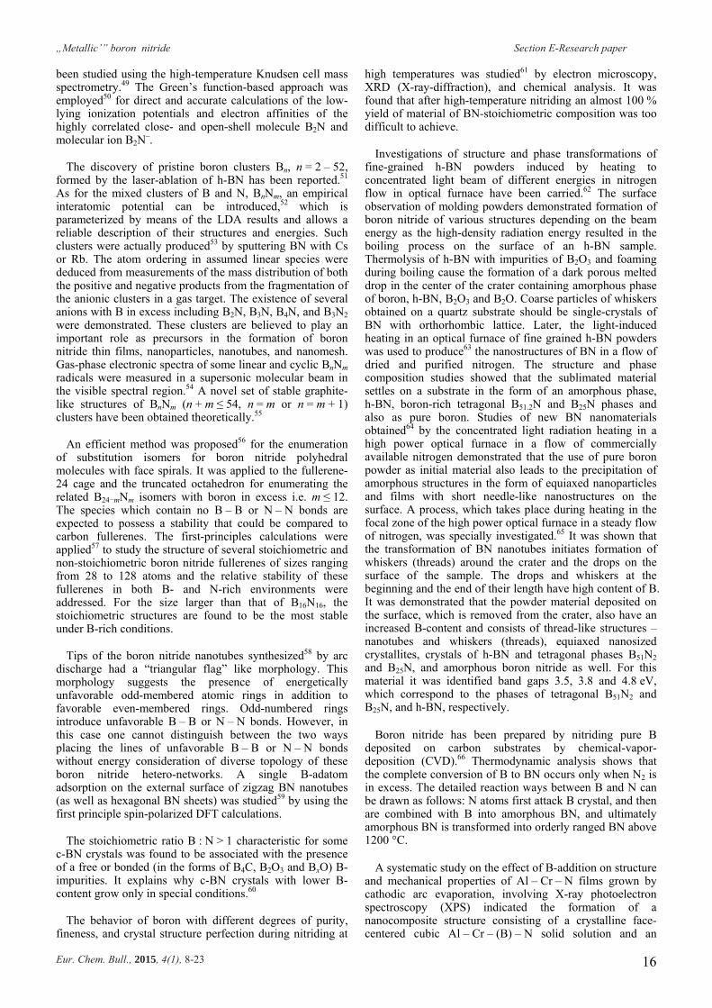
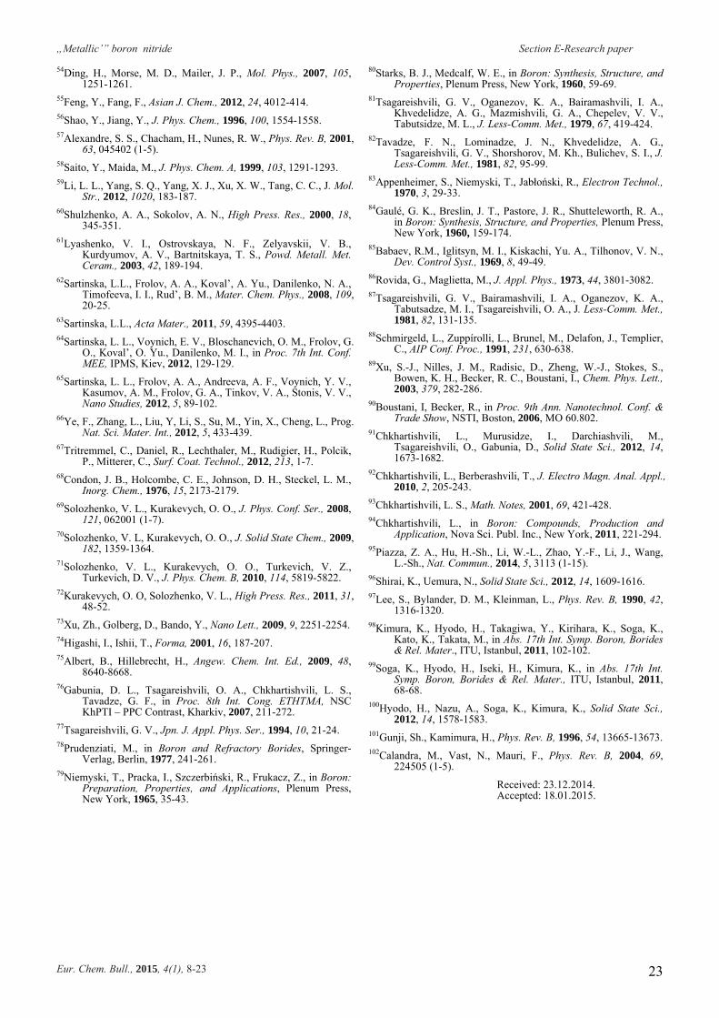
Chemical composition was analyzed for several different segments of shiny and dark surfaces. Examples of corresponding curves are presented in Figures 11 and 12. Figure 13 corresponds to the special case of fragments with flake-like structure.
(a)
(b)
(c)
Figure 11. Chemical composition of a fragment of outer shell-surface: (a) unallocated, (b) BK / CK and (c) sum spectra.
Numerical results of such analysis are presented in Table 1. It shows that on outer surface elements are distributed almost homogeneously. There are presented mainly B and C. Concentration of N is relatively low. O and other trace elements are not detectable. As for the inner surface, it reveals essentially inhomogeneous distribution of chemical elements. Concentrations of B and C remain high, but at the same time concentration of N also reaches the significantly high level.
(a)
(b)
(c)
(d)
(e)
Figure 12. Chemical composition of a fragment of inner shell-surface: (a) unallocated, (b, c) BK / CK, (d) NK /BK / CK, and (e) sum spectra.

„Metallic’” boron nitride Section E-Research paper
Eur. Chem. Bull., 2015, 4(1), 8-23 15
Now O is a detectable element. It should be emphasized that highest concentration of N is characteristic for flake-like microstructures: B 55.31, N 40.21 and C 4.48 atom %, respectively.
Figure 13. Chemical composition of flakes on inner shell-surface.
Because samples are thin polycrystalline structures, which are the most fragile material, it was extremely difficult to make rigorous electrical contact without turning them to dust. The probes used in electrical measurements were the brass spring-loaded hook-clips. However, even their pressure, necessary to get a reading, frequently destroyed such samples. It is a reason why we were only able to get momentary readings. Measured resistance R is in the range of ~ 106 Ω. Taking R ~ 106 Ω and crude estimates for the geometry of experiment – distance between probes l ~ 1 cm, their diameter d ~ 10–1 cm, and sample thickness w ~ 10−2 cm, we can recalculate samples resistivity:
lRdw / ~ 103 Ω cm, which is significantly lower if compared with the room temperature intrinsic resistivity of insulating boron nitrides, e.g. h-BN: ~ 1013 Ω cm, or even semiconducting boron modifications, e.g. ground-state β-rhombohedral modification B ~ 105 (β-B): ~ 107 Ω cm. Thus, obtained shells certainly are better conductive – “metallic” if compared with boron and boron nitride with chemical formula BN.
Table 1. Chemical composition of obtained shells in atom %.
Surface elements Outer Inner
B 85.66 – 88.57 55.31 – 91.00 N 00.34 – 00.67 00.01 – 40.21 C 11.09 – 13.57 04.48 – 18.15 O and other traces 00.00 – 00.00 00.00 – 00.77
One more argument of the “metallicity” is circuit shortening effect caused by shell fragments when they are placed on an insulating surface: after application of the wall voltage between pair of distant points on a shell fragment surface, the material is instantly vaporized with a blinding flash of light. This test was repeated many times on the two opposing surfaces and it was noted that when the electrodes touched the shiny side it was harder to initiate an arc and the arcs were not as intense as they were on the black side which was extremely sensitive, and vaporized more completely with a brighter flash. So, one can feel confident in saying that there is a clear difference in the electrical conductivity of the two surfaces: the black surface is definitely more conductive.
On the Positions of Nitrogen
We can state that, the synthesized shells mainly are consisted of boron.
As for the concentration of carbon, it is too high but less than the level of ~ 20 atom % characteristic of boron carbides with approximate chemical formula B4C. Unit cell of a boron carbide B12+xC3–x, 0.1 < x < 1.7, is similar to that of α-rhombohedral boron B12 (α-B), unless it contains additional C – B – C, C – B – B or B – B– B atomic chains along the largest diagonal of the elemental rhombohedron. Consequently, material has to contain fine crystals of α-B and maybe boron carbides of different chemical compositions (about properties of crystalline boron and its implications on boron carbides see reference46).
Apparently, the fine crystals of β-B have to be present as well. They can contain carbon not only segregated at grain boundaries, but also dissolved in lattice up to a few atom %. However, we do not expect interstitial doping of β-B with C as accommodation of carbon atoms inside the large crystallographic voids characteristic of β-B lattice is virtually impossible because carbon atoms easily substitute boron atom in too many regular sites leading to the contraction of interatomic chemical bonds.
And finally, as the material is synthesized at very high temperature the inclusions of amorphous phase of boron (a-B) are excluded. Material can contain only small regions of randomized structure in the form of an association of both icosahedral and (quasi)planar boron clusters enriched with carbon.
Thus, the synthesized shells can be imagined as a boron-based fine-structured multiphase system including α-B, β-B and traces of a-B doped with C, as well as boron carbides of different compositions. But, all these bulk phases are semiconducting. “Metallicity” of their mixture must be attributed to the presence of nitrogen with overly high concentrations. Consequently, we need to systemize here the data available on B/N systems for construction of the structural model describing position of N dopant atoms in the obtained material, which can be named as “boron-rich boron nitride.”
B/N stoichiometries with B in excess
There are number of evidences that boron nitride molecules and clusters, fullerenes and nanotubes, as well as solid structures prefer the stoichiometries with boron in excess.
Optimum geometries and vibration spectra for different states of B2N molecule were obtained by the Hartree–Fock (HF) method.47 From a statistical thermodynamic analysis, B2N is found to be extraordinarily stable up to very high temperatures, whereas nitrogen-rich species BN2 dissociates spontaneously to B + N2 at all temperatures. The BNB radical was generated48 by the laser vaporization of solid BN and isolated noble gas matrices at helium temperatures. This radical also was indicated as an extraordinary stable linear species with the symmetric ground state, according to the calculation at the configuration-interaction (CI) level of the theory. The equilibriums involving the B2N molecule has
„Metallic’” boron nitride Section E-Research paper
Eur. Chem. Bull., 2015, 4(1), 8-23 16
been studied using the high-temperature Knudsen cell mass spectrometry.49 The Green’s function-based approach was employed50 for direct and accurate calculations of the low-lying ionization potentials and electron affinities of the highly correlated close- and open-shell molecule B2N and molecular ion B2N
–.
The discovery of pristine boron clusters Bn, n = 2 – 52, formed by the laser-ablation of h-BN has been reported.51 As for the mixed clusters of B and N, BnNm, an empirical interatomic potential can be introduced,52 which is parameterized by means of the LDA results and allows a reliable description of their structures and energies. Such clusters were actually produced53 by sputtering BN with Cs or Rb. The atom ordering in assumed linear species were deduced from measurements of the mass distribution of both the positive and negative products from the fragmentation of the anionic clusters in a gas target. The existence of several anions with B in excess including B2N, B3N, B4N, and B3N2 were demonstrated. These clusters are believed to play an important role as precursors in the formation of boron nitride thin films, nanoparticles, nanotubes, and nanomesh. Gas-phase electronic spectra of some linear and cyclic BnNm radicals were measured in a supersonic molecular beam in the visible spectral region.54 A novel set of stable graphite-like structures of BnNm (n + m ≤ 54, n = m or n = m + 1) clusters have been obtained theoretically.55
An efficient method was proposed56 for the enumeration of substitution isomers for boron nitride polyhedral molecules with face spirals. It was applied to the fullerene-24 cage and the truncated octahedron for enumerating the related B24−mNm isomers with boron in excess i.e. m ≤ 12. The species which contain no B – B or N – N bonds are expected to possess a stability that could be compared to carbon fullerenes. The first-principles calculations were applied57 to study the structure of several stoichiometric and non-stoichiometric boron nitride fullerenes of sizes ranging from 28 to 128 atoms and the relative stability of these fullerenes in both B- and N-rich environments were addressed. For the size larger than that of B16N16, the stoichiometric structures are found to be the most stable under B-rich conditions.
Tips of the boron nitride nanotubes synthesized58 by arc discharge had a “triangular flag” like morphology. This morphology suggests the presence of energetically unfavorable odd-membered atomic rings in addition to favorable even-membered rings. Odd-numbered rings introduce unfavorable B – B or N – N bonds. However, in this case one cannot distinguish between the two ways placing the lines of unfavorable B – B or N – N bonds without energy consideration of diverse topology of these boron nitride hetero-networks. A single B-adatom adsorption on the external surface of zigzag BN nanotubes (as well as hexagonal BN sheets) was studied59 by using the first principle spin-polarized DFT calculations.
The stoichiometric ratio B : N > 1 characteristic for some c-BN crystals was found to be associated with the presence of a free or bonded (in the forms of B4C, B2O3 and BxO) B-impurities. It explains why c-BN crystals with lower B-content grow only in special conditions.60
The behavior of boron with different degrees of purity, fineness, and crystal structure perfection during nitriding at
high temperatures was studied61 by electron microscopy, XRD (X-ray-diffraction), and chemical analysis. It was found that after high-temperature nitriding an almost 100 % yield of material of BN-stoichiometric composition was too difficult to achieve.
Investigations of structure and phase transformations of fine-grained h-BN powders induced by heating to concentrated light beam of different energies in nitrogen flow in optical furnace have been carried.62 The surface observation of molding powders demonstrated formation of boron nitride of various structures depending on the beam energy as the high-density radiation energy resulted in the boiling process on the surface of an h-BN sample. Thermolysis of h-BN with impurities of B2O3 and foaming during boiling cause the formation of a dark porous melted drop in the center of the crater containing amorphous phase of boron, h-BN, B2O3 and B2O. Coarse particles of whiskers obtained on a quartz substrate should be single-crystals of BN with orthorhombic lattice. Later, the light-induced heating in an optical furnace of fine grained h-BN powders was used to produce63 the nanostructures of BN in a flow of dried and purified nitrogen. The structure and phase composition studies showed that the sublimated material settles on a substrate in the form of an amorphous phase, h-BN, boron-rich tetragonal B51.2N and B25N phases and also as pure boron. Studies of new BN nanomaterials obtained64 by the concentrated light radiation heating in a high power optical furnace in a flow of commercially available nitrogen demonstrated that the use of pure boron powder as initial material also leads to the precipitation of amorphous structures in the form of equiaxed nanoparticles and films with short needle-like nanostructures on the surface. A process, which takes place during heating in the focal zone of the high power optical furnace in a steady flow of nitrogen, was specially investigated.65 It was shown that the transformation of BN nanotubes initiates formation of whiskers (threads) around the crater and the drops on the surface of the sample. The drops and whiskers at the beginning and the end of their length have high content of B. It was demonstrated that the powder material deposited on the surface, which is removed from the crater, also have an increased B-content and consists of thread-like structures – nanotubes and whiskers (threads), equiaxed nanosized crystallites, crystals of h-BN and tetragonal phases B51N2 and B25N, and amorphous boron nitride as well. For this material it was identified band gaps 3.5, 3.8 and 4.8 eV, which correspond to the phases of tetragonal B51N2 and B25N, and h-BN, respectively.
Boron nitride has been prepared by nitriding pure B deposited on carbon substrates by chemical-vapor-deposition (CVD).66 Thermodynamic analysis shows that the complete conversion of B to BN occurs only when N2 is in excess. The detailed reaction ways between B and N can be drawn as follows: N atoms first attack B crystal, and then are combined with B into amorphous BN, and ultimately amorphous BN is transformed into orderly ranged BN above 1200 °C.
A systematic study on the effect of B-addition on structure and mechanical properties of Al – Cr – N films grown by cathodic arc evaporation, involving X-ray photoelectron spectroscopy (XPS) indicated the formation of a nanocomposite structure consisting of a crystalline face-centered cubic Al – Cr – (B) – N solid solution and an

„Metallic’” boron nitride Section E-Research paper
Eur. Chem. Bull., 2015, 4(1), 8-23 17
amorphous phase a-BNx, x < 1.67 The formation of a BNx phase is likely, although this phase, due to its often amorphous character, is not visible in the XRD pattern. It was evident from the spectra that the increasing B content is associated with an increase of the intensity and fraction of the B – N peak. This can be interpreted by an increasing fraction of a-BNx phase with increasing B content.
Crystalline boron nitrides with B in excess
At very high temperatures, B/N system forms mixtures of phases of boron and boron nitrides with boron in excess.
For this system, the existence of boron subnitride B6N with α-B-like structure was for the first time suggested as early as in 1976,68 by an examination of the direct solid – diatomic gas reaction between boron and nitrogen in the elevated temperature range from 1480 up to 1820 K. The reaction mechanism is most likely topochemical, i.e., with rate limited by the process occurring at the interface between the reaction product and the solid reactant, yielding BN with amorphous boron, probably of an α-B-like structure, as the starting material, while a two-step reaction series occurs with an homogenous reaction to form B6O followed by a topochemical reaction to yield BN when β-B is the starting material. Later, a number of boron subnitrides of different stoichiometries, e.g., B4N, have been reported; however, neither their structure nor thermodynamic stability has been established.
Rhombohedral boron subnitride B13N2 was synthesized69 by crystallization from the B/BN melt at 5 GPa. It represents a structural type produced by the distorted B12 icosahedra linked together by N – B – N chains and inter-icosahedral B – B bonds. According to the Raman data, the subnitride belongs to a group of boron-rich compounds with structures related to α-B. The composition B13N2 is less stable than boron nitride phases of composition BN. The details of chemical interaction and phase transformations in the B/BN system were studied70 in situ by XRD with synchrotron radiation at high temperatures and high pressures using multi-anvil press. The heating above 2380 K is accompanied by the disappearance of the β-B lines due to the boron melting. The quenching of the samples having the B6N and B5N compositions from 2400 to 2600 K leads to the formation of the well-crystallized rhombohedral boron subnitride phase with structure related to α-B and of general stoichiometry B12+xN2+y. XRD patterns of the well-powdered quenched samples shows the lines corresponding to a B6O-like lattice. The lattice parameters of this boron nitride are intermediate between those of boron suboxide B6O and boron carbide B13C2. The B12+xN2+y phase features distorted B12 icosahedra linked by N – B – N atomic chains, giving rise to a 3D framework. The similarity is greatest to B4+zC1–z, which has the same unit cell, space group, and atom sites as the subnitride. The site occupancies of the atoms of each crystallographic type are close to unit, so the synthesized phase has the B13N2 stoichiometry. The variation of lattice parameters of the as-synthesized B12+xN2+y subnitride in all experiments was too small, which allows one to conclude that the resulting phase B13N2 is an individual subnitride and not a solid solution (in contrast to boron carbide analog). Over the whole p – T -range under study, B13N2 crystallizes in mixture with β-B, a phase similar to boron-rich tetragonal subnitride B50N2 (a phase with structure of hypothetical first
tetragonal boron I-B) and h-BN. The amount of the B13N2 phase in relation to B50N2-like phase increases with a higher BN content in the starting mixture; however, synthesis of single-phase B13N2 seems to be impossible because its formation at ~5 GPa occurs according to the liquid + h-BN ↔ B13N2 peritectic reaction. Results of an in situ study71 of chemical interaction and phase relations in the B/BN system at pressure of ~ 5 GPa and temperatures up to 2800 K point to the contact interaction that gives rise to a metastable liquid in the system according to the B + h-BN ↔ liquid eutectic reaction, whose temperature is 2120 K. On subsequent heating to 2200 – 2250 K, the lines of B13N2 boron subnitride appear in the XRD patterns. It is the only thermodynamically stable boron subnitride, which melts incongruently at 2600 K and forms eutectic equilibrium with B at 2300 K and 4 atom % N.
These results on high-pressure synthesis of novel boron-rich solids, including boron-rich B/N phases, were summarized in a review.72 The phase equilibria studies in the B/BN system by both in situ experiments and thermodynamic calculations have revealed the existence of at least three different boron subnitrides.
First, the high pressure synthesis of the so-called B6N, the thermodynamically stable boron subnitride, was reported. However, its structure is unsolved. According to the simulations, it cannot belong to the α-B12 family. Second boron subnitride, having the diffraction pattern similar to that of B50N2, seems to be a B50N2−xBx solid solution, so-called I-tetragonal boron, boron-rich quasi-periodic structure stabilized by nitrogen contamination, since its formation is observed only in the presence of BN, while the lattice parameters correspond to those expected for B50N2. The formation of third subnitride was observed which has a well-pronounced α-B12-like powder XRD pattern. Its structure was resolved and represents a structural type produced by the distorted B12 icosahedra linked by the atomic chains N – B – N. The stoichiometry of the phase is B13N2. Rhombohedral B13N2 was found to be the only thermodynamically stable boron subnitride at ~ 5 GPa. From the phase diagram of the system constructed by adjustment of the calculated equilibrium lines to the experimental data, B13N2 melts incongruently at 2600 K, according to the liquid + BN → B13N2 peritectic reaction, and forms an eutectic equilibrium with β-B~ 105 at 2300 K.
Joule-heating-induced failure of individual multi-walled BN nanotubes was investigated73 in a high-resolution-transmission-electron-microscope (HRTEM) equipped with a scanning tunneling microscope unit. Direct observation of the failure process indicated that it occurred via thermal decomposition of tubular layers from inside-out of a tube leaving amorphous ball-like boron-based nanoparticles behind.
Local geometries in boron nitrides with B in excess
From the above discussion, one can conclude that all the boron nitride phases with B in excess, including the material obtained in the present work, can be imagined as mixtures of various boron modifications heavily doped with N. Since boron icosahedron B12 is known to be the main structural motif of these crystals, the feasible local geometries of environments of N atoms in boron-rich B/N systems can be

„Metallic’” boron nitride Section E-Research paper
Eur. Chem. Bull., 2015, 4(1), 8-23 18
constructed on the basis of crystal structure data on B12-icosahedral networks examined, for example, by Higashi and Ishii.74
In the α-B crystal, B12 icosahedra are placed at each corner of the rhombohedral unit cell. Linkages between the icosahedra are affected along the 5-fold axis in the direction of the main crystallographic axes. There appear three icosahedral networks, each with translational periodicity along the [111]-axis. They are all crystallographically equivalent, extending parallel to the (111)-plane. The linkages between B12 icosahedra within each network are by a 3-centered bond. On the other hand, linkages between icosahedral networks are made by 2-centered bond along the 5-fold axes of icosahedra in the direction of the main crystallographic axes. In the structure of B12N2 (B6N), which is of α-B structure-type, two nitrogen atoms are located on the [111]-axis in such a way that each of them is located at the center of a triangle formed with three icosahedra B12 (see Figures 14 and 15). Owing to the incorporation of N atoms, the rhombohedral unit cell volume is increased slightly with a variation of the rhombohedral angle. The recent data on lattice parameters of some B6N-related structures were presented by Albert and Hillebrecht.75
Figure 14. Structure of B6N (α-B structure-type). Each circle at the lattice point stands for the B12 icosahedron and smaller ones on the [111]-axis are N atoms.
Figure 16 shows the crystal structure of α-tetragonal boron. There are four icosahedra B12 per unit cell. In ideal structure, they coordinate tetrahedrally about an isolated B atom. But, it was reported that the accurate chemical composition of this crystal phase can be B50N2, and in real crystals the isolated B atoms should be replaced with N atoms. The icosahedral networks in B50N2 are, however, exactly the same as those in α-tetragonal boron.
Nitrogen in boron crystals
An overview of the studies in doping of β-B, including doping with N, has been given by us.76 Main conclusions are as following. Nitrogen not only forms compound with boron, but also can be accommodated in large crystallographic voids of the β-B lattice.
Like other light elements, N is hardly removable from β-B.77 According the microanalysis,78 distribution of N impurity atoms in β-B is inhomogeneous.
Figure 15. B12-icosahedral network in the structure of B6N as seen along the [111]-axis. The smaller circles stand for the N atoms.
Figure 16. Structure of α-tetragonal boron as seen along the c-axis. The larger cycles stands for the B12 icosahedra and the smaller ones for the isolated N atoms. Each of the isolated N atoms is tetrahedrally coordinated with four icosahedra B12.
Melting of boron in crucibles lined with boron nitride leads to the contamination of product with nitrogen: formation of a huge number of centers of crystallization and, consequently, crystallites.79 Especially fragile samples of β-B are obtained during melting in nitrogen-containing atmosphere. In case of melting directly in BN crucibles, such crystallites form a crust around a coarse-crystalline core.80 The β-B samples obtained by zone-melting of the pressed powders, in which H3BO3 served for binder material, contained gaseous impurities such as H, N and O.81,82 Thermal-kinetic analysis exhibits a basic trend: decreasing in N content leads to the increasing in O and H contents. It weakens twinning and increase micro-strength and deformation energy. In β-B crystals doped by diffusion of N in the melt, the concentration of unpaired spins increases.83,84 Corresponding electron-spin-resonance (ESR) line disappears only after a high-temperature annealing. Thermal treatment of β-B samples in nitrogen atmosphere can decrease their conductivity by ~ 200 %.85

„Metallic’” boron nitride Section E-Research paper
Eur. Chem. Bull., 2015, 4(1), 8-23 19
A low-energy-electron-diffraction (LEED) pattern, which is characteristic of the (111)-surface of β-B, was obtained86 after heating at a temperature higher than 1400 °C. As indicated by Auger spectroscopy, this treatment is sufficient to eliminate O and C, the main impurities present on the initial surface. However, a certain amount of N remains on the surface. On heating up to 1200 °C, the LEED pattern showed a completely disordered surface structure. In order to obtain a clean surface, the material was subjected to heat treatment at > 1300 °C and the vacuum attained in the apparatus was better than ~ 10–9 Torr. These conditions are necessary for recrystallization (α ↔ β transition) of boron.
As shown by Auger spectrometry, O was below the sensitivity limits, but small amounts of C and N were presented. No peaks of other elements were found. The amount of C seems too low to affect the surface structure. As for the N, it can be removed only by ion bombardment with Ar ions, but N reappears after the high-temperature heating necessary in order to reobtain a regular surface structure. This indicated that N is segregated near the surface and it is not ruled out if N diffuses from the bulk. The minimum ratio between N and B Auger peaks was about 1 : 50. The surface covered by this contamination should be of the order of one-tenth of a monolayer what can affect the surface structure of the β-B.
In the work87 curried out to study the interaction of fine grained boron powders with gaseous environment and develop a technique for removal of gases from powders, we determined the content of N2 from the analysis by the reduction melting method. In powders with average particles sizes of 1.90, 0.46 and 0.25 μm, there were determined 0.9, 0.5 and 2.1 wt. % N2, respectively.
Studying88 the ion implantation in boron leads to the undisputable result that in the absence of a significant concentration (a few tenths atom %) of N no amorphization takes place in β-B implanted with N-ions. This result can be understood taking into account following two factors: (i) about ⅓ of the valence electrons in boron icosahedron are directed towards external bonds and their number and directions can be easily changed in order to adopt it to surroundings, giving rise only distortions from the regular configuration, and greater stability and versatility to the icosahedron; (ii) the β-B lattice affords eighteen vacant voids per hexagonal unit cell and can accommodate impurity concentrations of the stopping range of the order of 3 · 1021 cm–3. As for the boron nitrides of composition BN, whose structure is not built of icosahedra, they are known to be damaged very easily by irradiation even at very low doses.
Structural model of nitrogen-doped boron
Structural patterns of boron nitrides with excess of boron allow the constructing of the structural model for nitrogen impurity centers in boron matrix.
Previously, we reported89 a mass spectrometric study of boron cluster anions Bn
–, n = 7 – 55, containing multiple B12-icosahedra, which were produced by laser vaporization both from pure boron (i.e. homogeneous) and boride (i.e. heterogeneous) target rods. While at lower masses these spectra were similar, at higher masses the boride spectrum
exhibited a completely different pattern: in addition to the local maximum at B13
–, characteristic of the pure boron spectrum as well, a repeating intensity pattern having local maxima at (B13
–)(B12)2 and (B13–)(B12)3 as well as (B13
–)(B13) were observed. These observations can be attributed to the structural differences between the two target materials. The appearance of B12 units in the boride mass spectrum is presumably due to the ablation of relatively labile B12 cages from the structure. The fusion of two B12 units, followed by their asymmetric dissociation upon electron attachment into B13
– + B11 or B11– + B13 explains why both clusters B13
– and B11
– display higher intensities than their immediate neighbors in both the pure boron and the boride mass spectra. As for the relative prominence of B13
–-based species over B11
–-based ones in the mass spectra, it may be due to B13 having a higher electron affinity than B11 and also stability of B13
– with regard to electron loss. Further, we had demonstrated90 that created boron clusters can be self-assembled into nanostructures.
Taking into account high content of carbon, we cannot rule out that in addition to carbon-doped boron allotropes the synthesized material contains some amounts of boron carbide phases with crystalline lattices similar to that of α-B, which are semiconducting like this and all the rest crystalline modifications of boron.
From these studies and the above described results available in literature on B/N stoichiometries, crystalline boron nitrides, and local geometries in boron nitrides with B excess as well as on the behavior of nitrogen in boron crystals, we can figure out structure of possible atomic environments of N impurity atoms in synthesized material.
In crystallites of B12N2, nitrogen atoms are surrounded by 3 boron atoms, which are symmetrically placed in the same plane, i.e. like the intralayer coordination in h-BN. We can, therefore, approximate corresponding B – N chemical bonds length by that of h-BN: 1.45 Å. Not truly identical, but similar local environment would be realized in crystallites of B12N2, α-B doped with N (i.e. with no more than one N atom in the unit cell), and boron carbides doped with N (i.e. with one or two B or C atoms in the unit cell substituted with N atoms).
In crystallites of B50N2, nitrogen atoms are tetrahedrally surrounded by 4 boron atoms, i.e. like the coordination in c-BN. For this reason, we can approximate corresponding B – N bonds length by that of c-BN: 1.57 Å.
And finally, in crystallites of β-B, impurity atoms of nitrogen can be accommodated in crystallographic voids of types A(1), A(2), A(3), D and E with 12, 12, 12, 14 and 15 neighboring boron atoms and B – N bonds average length of 2.17, 2.10, 2.15, 2.36 and 2.38 Å, respectively. In crystallites of I-B, the situation must be almost similar, unless part of N atoms is substituted by other impurities, which possibly also stabilize the structure.
As for the flakes found in our material, their layered structure and chemical composition with highest nitrogen and relatively low carbon contents and small excess of boron point to the local formations of h-BN doped with carbon (i.e. h-BNC) together with small amount of boron-rich phases doped with nitrogen.

„Metallic’” boron nitride Section E-Research paper
Eur. Chem. Bull., 2015, 4(1), 8-23 20
Theorizing
Finding out the electron energy levels of dopant nitrogen accommodated in various boron-rich lattices requires development of a special model of impurity centers. The situation when the nitrogen atom is introduced among boron atoms, already tightly bonded together, essentially differs from that when a tightly bonded with neighbors constituent boron atom is substituted. Therefore, standard models for impurity centers cannot be used for our purposes. The appropriate model was proposed and successfully applied for β-B doped with metals by us earlier.91 Taking into account that such an impurity atom only slightly affect the crystalline structure, within the first approximation the donor energy level of the impurity atom can be found from the outer valence shell ionization potential of the same chemical element in isolated state shifting the corresponding electron energy level in the internal crystalline field. This chemical shift can be found assuming that changes in the electric field within an impurity atom are determined mainly by the boron atoms directly surrounding it. Within the proposed model, the depth of the donor level ED formed by the nitrogen impurity atom embedded in a certain boron-rich crystallite is determined from the relation
(1)
where EIP is the known ionization potential of N atom in the
isolated state, EIP=14.53 eV, and E'IP is its shift in the crystalline field, while EWF and EG are the electron work function and the band gap of the semiconductor. In case of β-B, EWF= 6.13 eV and EG=1.56 eV. This value for work function is chosen by us on the basis of analysis of the existing experimental data. As for α-B and I-B, there are no data available for their work function. That is why in all the cases below we use the difference EWF – EG = 6.13 eV – 1.57 eV = 4.56 eV assuming that it is almost the same for all crystalline modifications of boron.
Thus, to find the location of nitrogen donor levels on the energy axis it is necessary to calculate only one quantity, E'IP. It is possible to estimate its value as a quantum-mechanical mean of the electron potential energy in the crystalline field. In the initial quasi-classical approximation we obtain:
IP IPIP i i IP IP2 2
IP IP IP IP IP IP 1
3 2' ( , , )
4 (4 ( 1)) ( 1)
i q
i
NE EE V r r d
n l l n l l
(2)
Here N is the coordination number – number of boron atoms surrounding the impurity nitrogen atom, and d is the B – N bonds average length; function Vi(r'IP, r″IP, d) denotes the volume of the intersection of i th layer of the boron atom with the layer of the nitrogen atom limited by the classical turning points radii r'IP and r″IP of the outer valence shell electron:
(3)
(4)
where nIP and lIP represent, respectively, the principal and orbital quantum numbers of the outer valence shell electron in the impurity atom. For nitrogen nIP = 2 and lIP = 1.
The function Vi(r'IP, r″IP, d) is calculated as a linear combination of intersection volumes of 4 pairs of spheres:
(5)
Here the coefficient i is the volume-average of the electric field potential in the i th radial layer of boron atom, q is the number of layers of the quasi-classical averaging. The parameters ri and ri–1 are the external and internal radii of the i th layer of boron atom, respectively (assuming r0
≡ 0). For B atom the parameter q = 5. As for the ri and i, they are given in Table 2. Their numerical values have been calculated and tabulated in ref.92 The function V(r1, r2, d12) has a geometric meaning as the volume of an intersection of two spheres with radii 1r and 2r whose centers are at the distance 12d from each other. It is an algebraic piecewise continuous function. Explicit form of V(r1, r2, d12) has been described.93
Table 2. Quasi-classical parameters of potential distribution in B atom.
i ri, a.u. i, a.u.
1 2.758476 E–2 + 2.105468 E+2 2 5.098016 E–1 – 8.882329 E+0 3 7.441219 E–1 – 3.652920 E+0 4 4.021346 E+0 – 2.060720 E–1 5 4.337060 E+0 – 6.135348 E–4
Table 3. Parameters of N donor centers in boron crystals.
Structure Site N d, Å ED, eV
α-B 3 1.45 – 5.2 A(1) 12 2.17 –12.3 A(2) 12 2.10 –14.0 A(3) 12 2.15 –12.8
D 14 2.36 –11.1
β-B
E 15 2.38 –12.1 I-B 4 1.57 – 8.7
The calculated electron energy levels together with parameters of corresponding impurity centers are summarized in Table 3. Thus, all the DE < 0, i.e. N-related donor levels are placed immediately inside the conduction band or even above the vacuum level. In this context it should be noted that the calculated negative energy levels of
2IP IP IP IP
IP
IP
( 1)
2
n n l lr
E
2IP IP IP IP
IP
IP
( 1)
2
n n l lr
E
D IP IP WF G( ) ( )E E E E E
i IP IP
i IP i 1 IP i IP i 1 IP
( , , )
( , , ) ( , , ) ( , , ) ( , , )
V r r d
V r r d V r r d V r r d V r r d

„Metallic’” boron nitride Section E-Research paper
Eur. Chem. Bull., 2015, 4(1), 8-23 21
course are definitely virtual and they never can be occupied. These dopant atoms supply electrons at first to low-lying electron traps located within the band gap and then to delocalized electron states at the bottom of the conduction band, i.e., they cause metallization of the material when introduced at sufficiently high concentrations.
Main result of the present calculations is that the N atoms in BNx act as electron-donors. The same can be argued from the following qualitative consideration. Boron is known to be one of the most electronegative elements, but it is less electronegative than nitrogen. For this reason, in common boron nitrides with chemical formula BN, the electron density is shifted from B atoms towards N atoms. However, in boron nitrides with excess of boron, BNx, x << 1, boron atoms enable to form icosahedra and other multi-atomic clusters, significantly enhancing in this way the electronegativity of the boron component. Thus, the electron density can be shifted from N atoms towards B clusters.
Presence of traces of boron nanophases in the material obtained cannot be rules out. The nanophases are expected to be metallic.94 Recently, it has been proposed95 that the so-called borophene, the structure built up from planar hexagonal B36 clusters, must be fully metallic. However, it seems too doubtful that amount of nanoboron-component is enough to form a continuous conductive matrix. Thus, the metallization related to doping phases of semiconducting boron, and maybe boron carbide inclusions, with nitrogen seems to be prevailing.
Conclusion
In summary, the “metallic” conductivity in boron nitride with boron in excess can be explained in a way similar to that of boron doped with metals. It means that such a material can be modeled as a mix of boron phases heavily doped with nitrogen impurity.
In this regard, it is appropriate to discuss the phenomena of metallic conductivity and superconductivity in boron crystals.
A long-standing issue, why β-B, with odd number of electrons in the regular unit cell, which, as the band calculations predict, was to be metallic, is in fact semiconducting, has been solved.96 The problem was related to the breaking of stoichiometry in this crystal: the presence of unfilled bands requires reconstruction of chemical bands.
As for α-B, using an expansion of plane waves, the first principles calculations of the energy bands of B12 were performed97 which found a gap of width 1.427 eV, i.e. α-B must be a semiconductor.
A unified picture for B-based icosahedral cluster solids has been proposed.98 The common features are: (i) they are expected to have complicated structures such as giant unit cell crystals or quasi-crystals because of inconsistency between the icosahedral symmetry and the space periodicity, (ii) they can have both metallic and covalent bonds, because B is located at the boundary of covalent/metallic bonding in the Periodic Table, (iii) their Fermi level can be located in the deep pseudo-gap or at the high DOS position because of
high symmetry of the icosahedron. The metallic–covalent bonding conversion in boron can occur at sites other than the center of the icosahedron. In particular, when a vanadium V atom is doped in the certain-type crystallographic void of β-B, the bonding nature is converted from the covalent one to the more metallic one. A characteristic phenomenon in the V-doped β-B is the change of electrical conductivity from that of semiconducting hopping-type into metallic one by doping with only ~ 1 atom % V.99 This unique conversion of electrical conductivity seems to be due to the local metallic–covalent bonding conversion. A high concentration of lithium Li (up to the composition LiB5.8, i.e. 18 Li atoms per cell) was doped into β-B.100 In Li- or Mg-doped β-B, electron doping was compensated by removing of interstitial B atoms and by generating of vacancies.
Theoretical exploration of a group of B12-based materials, AxB12, with A = Li and Ca, and x = 1 – 4, was done101 by performing LDA calculations of the electronic structure, including DOS, using the first principles pseudopotentials. Li-doped materials mostly demonstrate to be sufficiently stable, whereas it is shown that all calcium-doped materials are unstable, including Li2CaB12. These calculations showed essentially metallic behavior of stable and metastable LixB12. Favorable superconducting properties were predicted for Li3B12, in the context of the sufficiently high DOS at the Fermi energy and obtained bulk modulus that is indicative of strong electron–phonon coupling.
An alternative route to achieve the superconducting state in boron-rich solids has been proposed, the hole-doping of B12 icosahedra.102 For this purpose a prototype metallic phase of B13C2 was considered. It was shown that in this compound the boron icosahedral units are mainly responsible for large phonon frequencies and moderate electron–phonon coupling. It was suggested that relatively high critical temperature could be a general feature of hole-doped boron icosahedral solids.
Thus, boron, heavily doped with metal impurities, exhibits metallic conductivity and even superconductivity.
As for the boron “doped” with nitrogen, i.e., boron nitride with boron in excess, there is only single indirect experimental evidence of its “metallicity” mentioned above. It was predicted that superhard rhombohedral subnitride B13N2 might exhibit metallic conductivity. Unfortunately, the B13N2 crystallization by peritectic reaction in the studied
Tp range did not allow the study of such properties. Taking into account (i) metallic behavior and even superconductivity observed in boron-rich solids at high pressure and (ii) the results on high-pressure synthesis of novel boron-rich solids, including boron-rich B/N phases, reviewed above, one may expect that these high pressure phases can have exceptional electronic and phonon transport properties.
The theoretical results obtained in the present work for N-doping of boron quantitatively support already suggested qualitative mechanism of modification of the electronic properties of boron by doping. Initially electrons from donor impurities fill the empty intrinsic acceptor levels. It leads to an increase in the concentration of hole-hopping centers and, consequently, p-type hopping conductivity also increases. However, after about a half of these centers have been filled,

„Metallic’” boron nitride Section E-Research paper
Eur. Chem. Bull., 2015, 4(1), 8-23 22
a decrease in the concentration of localized holes prevails and the hopping conductivity begins to decrease as well. At higher dopant concentrations, when all of acceptor centers of intrinsic origin are occupied by electrons, the inversion of type of conduction takes place, and the n-type conductivity starts to increase. Finally, the doping of boron with donor atoms at sufficiently high concentrations yields the metallization of the material – a semiconductor-to-semimetal transition.
Acknowledgements
The authors wish to thank especially Perry Phillips for his laboratory assistance to Rick Becker.
References
1Chkhartishvili, L., Lezhava, D., Tsagareishvili, O., Gulua, D., Proc. Police Acad. Georg., 1999, 1, 295-300.
2Chkhartishvili, L. S., Phys. Solid State, 2004, 46, 2126-2133. 3Chkhartishvili, L., Lezhava, D., Tsagareishvili, O., J. Solid State
Chem., 2000, 154, 148-152. 4Chkhartishvili, L., J. Solid State Chem., 2004, 177, 395-399. 5Chkhartishvili, L., Mater. Sci. Ind. J., 2006, 2, 18-23. 6Al’tshuler, A. M., Vekilov, Y. K., Umarov, G. R., High Temp.
High Press., 1976, 8, 635-662. 7Zhang, Zh., Guo, W., Nano Lett., 2012, 12, 3650-3655. 8Zhang, Sh., Wang, Q., Kawazoe, Y., Jena, P., J. Am. Chem. Soc.,
2013, 135, 18216-18221. 9Hu, Sh., Zhao, J., Jin, Y., Yang, J., Petek, H., Hou, J. G., Nano
Lett., 2010, 10, 4830-4838. 10Srivastava, A., Sharma, M., Tyagi, N., Kothari, S. L., J. Comput.
Theo. Nanosci., 2012, 9, 1693-1699. 11Mousavi, H., J. Supercond. Novel Magn., 2013, 26, 2905-2909. 12Owens, F. J., Mol. Phys., 2011, 109, 1527-1531. 13Anota, E. Ch., Escobedo–Morales, A., Villanueva, M. S.,
Vázquez–Cuchillo, O., Rosas, E. R., J. Mol. Modeling, 2013, 19, 839-846.
14Du, A., Chen, Y., Zhu, Zh., Amal, R., Lu, G. Q. (M.), Smith, S. C., J. Am. Chem. Soc., 2009, 131, 17354-17359.
15Terrones, M., Charlier, J.-C., Gloter, A., Cruz–Silva, E., Terrés, E., Li, Y. B., Vinu, A., Zanolli, Z., Dominguez, J. M., Terrones, H., Bando, Y., Golberg, D., Nano Lett., 2008, 8, 1026-1032.
16Barone, V., Peralta, J. E., Nano Lett., 2008, 8, 2210-2214. 17Lai, L., Lu, J., Wang, L., Luo, G., Zhou, J., Qin, R., Gao, Zh.,
Mei, W. N., J. Phys. Chem. C, 2009, 113, 2273-2276. 18Tang, P., Zou, X., Wang, S., Wu, J., Liu, H., Duan, W., RSC Adv.,
2012, 2, 6192-6199. 19Li, X., Wu, X., Zeng, X. Ch., Yang, J., ACS Nano, 2012, 6, 4104-
4112. 20Wang, Y., Ding, Y., Ni, J., J. Phys. Chem. C, 2012, 116, 5995-
6003. 21Alem, N., Ramasse, Q. M., Seabourne, C. R., Yazyev, O. V.,
Erickson, K., Sarahan, M. C., Kisielowski, C., Scott, A. J., Louie, S. G., Zettl, A., Phys. Rev. Lett., 2012, 109, 126102 (1-5).
22Park, Ch.-H., Louie, S. G., Nano Lett., 2008, 8, 2200-2203.
23Chen, W., Li, Y., Yu, G., Li, Ch.-Zh., Zhang, Sh. B., Zhou, Zh., Chen, Zh., J. Am. Chem. Soc., 2010, 132, 1699-1705.
24Samarakoon, D. K., Wang, X.-Q., Appl. Phys. Lett., 2012, 100, 103107 (1-4).
25Zhang, H. X., Feng, P. X., ACS Appl. Mater. Interfaces, 2012, 4, 30-33.
26Lopez–Bezanilla, A., Huang, J., Terrones, H., Sumpter, B. G., J. Phys. Chem. C, 2012, 116, 15675-15681.
27Lopez–Bezanilla, A., Huang, J., Terrones, H., Sumpter, B. G., Nano Lett., 2011, 11, 3267-3273.
28Lopez–Bezanilla, A., Huang, J., Terrones, H., Sumpter, B. G., Nano Lett., 2012, 12, 3879-3879.
29Guo, Y., Guo, W., Nanoscale, 2014, 6, 3731-3736. 30Anota, E. C., Gutiérrez, R. E. R., Morales, A. E., Cocoletzi, G. H.,
J. Mol. Modeling, 2012, 18, 2175-2184. 31Mousavi, H., Moradian, R., Solid State Commun., 2013, 153, 17-
22. 32Berseneva, N., Gulans, A., Krasheninnikov, A. V., Nieminen, R.
M., Phys. Rev. B, 2013, 87, 035404 (1-9). 33Zeng, J, Chen, K.-Q., Sun, C. Q., Phys. Chem. Chem. Phys., 2012,
14, 8032-8037. 34Wang, Y., Ding, Y., J. Phys. Chem. C, 2013, 117, 3114-3121. 35Xue, Y., Liu, Q., He, G., Xu, K., Jiang, L., Hu, X., Hu, J.,
Nanoscale Res. Lett., 2013, 8, 49-55. 36Yan, B., Park, Ch., Ihm, J., Zhou, G., Duan, W., Park, N., J. Am.
Chem. Soc., 2008, 130, 17012-17015. 37Batista, R. J. C., de Oliveira, A. B., Pereira, N. R., Paolini, R. S.,
Manhabosco, T. M., J. Phys. Cond. Matter, 2012, 24, 165501 (1-10).
38Nakamura, J., Nitta, T., Natori, A., Phys. Rev. B, 2005, 72 205429 (1-5).
39Liu, Y., Wu, X., Zhao, Y., Zeng, X. Ch., Yang, J., J. Phys. Chem. C, 2011, 115, 9442-9450.
40Yu, Zh., Hu, M. L., Zhang, C. X., He, C. Y., Sun, L. Z., Zhong, J., J. Phys. Chem. C, 2011, 115, 10836-10841.
41Xiao, H. P., He, Ch., Zhang, Ch., Sun, L. Z., Peng, X., Zhang, K., Zhong, J., Physica B, 2012, 407, 4770-4472.
42Song, L., Balicas, L., Mowbray, D. J., Capaz, R. B., Storr, K., Ci, L., Jariwala, D., Kurth, S., Louie, S. G., Rubio, A., Ajayan, P. M., Phys. Rev. B, 2012, 86, 075429 (1-12).
43Zhou, Y., Wang, Zh., Yang, P., Gao, F., J. Phys. Chem. C, 2012, 116, 7581-7586.
44Menezes, M. G., Capaz, R. B., Phys. Rev. B, 2012, 86, 195413 (1-9).
45Li, X., Yang, W., Liu, B., Nano Lett., 2007, 7, 3709-3715. 46Wang, L., Mo, Y., Rulis, P., Ching, W. Y., RSC Adv., 2013, 3,
25374-25387. 47Martin, J. M. L., François, J. P., Gijbels, R., Chem. Phys., 1989,
90, 6469-6485. 48Knight Jr., L. B., Hill, D. W., Kirk, T. J., Arrington, C. A., J.
Phys. Chem., 1992, 96, 555-561. 49Meloni, G., Baba, M. S., Gingerich, K. A., J. Chem. Phys., 2000,
113, 8995-8999. 50Mahalakshmi, S., Yeager, D.L., Mol. Phys., 2003, 101, 165-174. 51la Placa, S. J., Roland, P. A., Wynne, J. J., Chem. Phys. Lett.,
1992, 190, 163-168. 52Albe, K., Möller, W., Heinig, K.-H., Radiat. Eff. Def. Solids,
1997, 141, 85-97. 53Vandenbosch, R., Phys. Rev. A, 2003, 67, 52709 (1-5).
„Metallic’” boron nitride Section E-Research paper
Eur. Chem. Bull., 2015, 4(1), 8-23 23
54Ding, H., Morse, M. D., Mailer, J. P., Mol. Phys., 2007, 105, 1251-1261.
55Feng, Y., Fang, F., Asian J. Chem., 2012, 24, 4012-414. 56Shao, Y., Jiang, Y., J. Phys. Chem., 1996, 100, 1554-1558. 57Alexandre, S. S., Chacham, H., Nunes, R. W., Phys. Rev. B, 2001,
63, 045402 (1-5). 58Saito, Y., Maida, M., J. Phys. Chem. A, 1999, 103, 1291-1293. 59Li, L. L., Yang, S. Q., Yang, X. J., Xu, X. W., Tang, C. C., J. Mol.
Str., 2012, 1020, 183-187. 60Shulzhenko, A. A., Sokolov, A. N., High Press. Res., 2000, 18,
345-351. 61Lyashenko, V. I., Ostrovskaya, N. F., Zelyavskii, V. B.,
Kurdyumov, A. V., Bartnitskaya, T. S., Powd. Metall. Met. Ceram., 2003, 42, 189-194.
62Sartinska, L.L., Frolov, A. A., Koval’, A. Yu., Danilenko, N. A., Timofeeva, I. I., Rud’, B. M., Mater. Chem. Phys., 2008, 109, 20-25.
63Sartinska, L.L., Acta Mater., 2011, 59, 4395-4403. 64Sartinska, L. L., Voynich, E. V., Bloschanevich, O. M., Frolov, G.
O., Koval’, O. Yu., Danilenko, M. I., in Proc. 7th Int. Conf. MEE, IPMS, Kiev, 2012, 129-129.
65Sartinska, L. L., Frolov, A. A., Andreeva, A. F., Voynich, Y. V., Kasumov, A. M., Frolov, G. A., Tinkov, V. A., Stonis, V. V., Nano Studies, 2012, 5, 89-102.
66Ye, F., Zhang, L., Liu, Y, Li, S., Su, M., Yin, X., Cheng, L., Prog. Nat. Sci. Mater. Int., 2012, 5, 433-439.
67Tritremmel, C., Daniel, R., Lechthaler, M., Rudigier, H., Polcik, P., Mitterer, C., Surf. Coat. Technol., 2012, 213, 1-7.
68Condon, J. B., Holcombe, C. E., Johnson, D. H., Steckel, L. M., Inorg. Chem., 1976, 15, 2173-2179.
69Solozhenko, V. L., Kurakevych, O. O., J. Phys. Conf. Ser., 2008, 121, 062001 (1-7).
70Solozhenko, V. L, Kurakevych, O. O., J. Solid State Chem., 2009, 182, 1359-1364.
71Solozhenko, V. L., Kurakevych, O. O., Turkevich, V. Z., Turkevich, D. V., J. Phys. Chem. B, 2010, 114, 5819-5822.
72Kurakevych, O. O, Solozhenko, V. L., High Press. Res., 2011, 31, 48-52.
73Xu, Zh., Golberg, D., Bando, Y., Nano Lett., 2009, 9, 2251-2254. 74Higashi, I., Ishii, T., Forma, 2001, 16, 187-207. 75Albert, B., Hillebrecht, H., Angew. Chem. Int. Ed., 2009, 48,
8640-8668. 76Gabunia, D. L., Tsagareishvili, O. A., Chkhartishvili, L. S.,
Tavadze, G. F., in Proc. 8th Int. Cong. ETHTMA, NSC KhPTI – PPC Contrast, Kharkiv, 2007, 211-272.
77Tsagareishvili, G. V., Jpn. J. Appl. Phys. Ser., 1994, 10, 21-24. 78Prudenziati, M., in Boron and Refractory Borides, Springer-
Verlag, Berlin, 1977, 241-261. 79Niemyski, T., Pracka, I., Szczerbiński, R., Frukacz, Z., in Boron:
Preparation, Properties, and Applications, Plenum Press, New York, 1965, 35-43.
80Starks, B. J., Medcalf, W. E., in Boron: Synthesis, Structure, and Properties, Plenum Press, New York, 1960, 59-69.
81Tsagareishvili, G. V., Oganezov, K. A., Bairamashvili, I. A., Khvedelidze, A. G., Mazmishvili, G. A., Chepelev, V. V., Tabutsidze, M. L., J. Less-Comm. Met., 1979, 67, 419-424.
82Tavadze, F. N., Lominadze, J. N., Khvedelidze, A. G., Tsagareishvili, G. V., Shorshorov, M. Kh., Bulichev, S. I., J. Less-Comm. Met., 1981, 82, 95-99.
83Appenheimer, S., Niemyski, T., Jabłoński, R., Electron Technol., 1970, 3, 29-33.
84Gaulé, G. K., Breslin, J. T., Pastore, J. R., Shutteleworth, R. A., in Boron: Synthesis, Structure, and Properties, Plenum Press, New York, 1960, 159-174.
85Babaev, R.M., Iglitsyn, M. I., Kiskachi, Yu. A., Tilhonov, V. N., Dev. Control Syst., 1969, 8, 49-49.
86Rovida, G., Maglietta, M., J. Appl. Phys., 1973, 44, 3801-3082. 87Tsagareishvili, G. V., Bairamashvili, I. A., Oganezov, K. A.,
Tabutsadze, M. I., Tsagareishvili, O. A., J. Less-Comm. Met., 1981, 82, 131-135.
88Schmirgeld, L., Zuppírolli, L., Brunel, M., Delafon, J., Templier, C., AIP Conf. Proc., 1991, 231, 630-638.
89Xu, S.-J., Nilles, J. M., Radisic, D., Zheng, W.-J., Stokes, S., Bowen, K. H., Becker, R. C., Boustani, I., Chem. Phys. Lett., 2003, 379, 282-286.
90Boustani, I, Becker, R., in Proc. 9th Ann. Nanotechnol. Conf. & Trade Show, NSTI, Boston, 2006, MO 60.802.
91Chkhartishvili, L., Murusidze, I., Darchiashvili, M., Tsagareishvili, O., Gabunia, D., Solid State Sci., 2012, 14, 1673-1682.
92Chkhartishvili, L., Berberashvili, T., J. Electro Magn. Anal. Appl., 2010, 2, 205-243.
93Chkhartishvili, L. S., Math. Notes, 2001, 69, 421-428. 94Chkhartishvili, L., in Boron: Compounds, Production and
Application, Nova Sci. Publ. Inc., New York, 2011, 221-294. 95Piazza, Z. A., Hu, H.-Sh., Li, W.-L., Zhao, Y.-F., Li, J., Wang,
L.-Sh., Nat. Commun., 2014, 5, 3113 (1-15). 96Shirai, K., Uemura, N., Solid State Sci., 2012, 14, 1609-1616. 97Lee, S., Bylander, D. M., Kleinman, L., Phys. Rev. B, 1990, 42,
1316-1320. 98Kimura, K., Hyodo, H., Takagiwa, Y., Kirihara, K., Soga, K.,
Kato, K., Takata, M., in Abs. 17th Int. Symp. Boron, Borides & Rel. Mater., ITU, Istanbul, 2011, 102-102.
99Soga, K., Hyodo, H., Iseki, H., Kimura, K., in Abs. 17th Int. Symp. Boron, Borides & Rel. Mater., ITU, Istanbul, 2011, 68-68.
100Hyodo, H., Nazu, A., Soga, K., Kimura, K., Solid State Sci., 2012, 14, 1578-1583.
101Gunji, Sh., Kamimura, H., Phys. Rev. B, 1996, 54, 13665-13673. 102Calandra, M., Vast, N., Mauri, F., Phys. Rev. B, 2004, 69,
224505 (1-5).
Received: 23.12.2014. Accepted: 18.01.2015.