electronic properties of heterostructures: graphene/boron...
TRANSCRIPT

Journal of Thi-Qar University Vol.11 No.2 June 2016
Theoretical Study Toward Understanding the Electronic Properties of Armchair Hetero Nanotubes
Laith A. AlgharagholyDepartment of Natural Science, College of Basic Education, University of
Sumer, Refayee, Dhi-Qar, Iraq.Department of Physics, Lancaster University, Visiting Researcher, Lancaster
LA1 4YB, UK. Email: [email protected]
Abstract
Using the density functional theory ‘DFT’ code ‘SIESTA’ combined with a Green’s function scattering approach ‘GFSA’ code ‘GOLLUM’, we investigate the electronic properties of hetero nanotubes, density of states ‘DOS’, electronic band structure BS, transmission coefficient T(E) and current-voltage curve. We simulated four different hetero structures of nanotubes which are: 1- Hetero nanotube with one graphene ring and one boron nitride ring. 2- Hetero nanotube with two graphene ring and one boron nitride rings. 3- Hetero nanotube with three graphene ring and one boron nitride rings. 4- Hetero nanotube with four graphene ring and one boron nitride rings nanotubes. The results show that there is a clear reduction in energy gap ‘Eg’ of hetero nanotubes comparing with the insulator boron nitride (Eg≈4.6 eV) and also this kind of hetero nanotubes have zero states at Fermi energy comparing with conductor carbon nanotube which has finite states at Fermi energy. This is could be a good method to design a semiconductor with desirable band gap.
Keywords: carbon nanotubes, boron nitride nanotubes, hetero nanotubes, energy gap.
35

Journal of Thi-Qar University Vol.11 No.2 June 2016
نظرية لألنابيب نحو دراسة الخصائصااللكترونية فهم التركيب المغايرة النانوية
القرغولي عبدالحسن ليث, , , , , قار ذي الرفاعي سومر جامعة االساسية التربية كلية العلوم قسم
العراق, , , , النكاستر جامعة زائر باحث النكاستر جامعة الفيزياء قسم
المتحدة البريد [email protected] .المملكة-:االلكتروني
الخالصة
الكثافة " نظرية كرين" DFTباستخدام دالة تقريب مع جنب إلى جنباالتشتت ' النانوية' GFSAلمنطقة لألنابيب اإللكترونية الخصائص دراسة تم ،
" ( الحاالت ( كثافة ، نترايد والبرون الكاربون من المركبة التركيب المغايرةDOS "االلكترونية الحزم تركيب ،EBS االنتقال معامل ،T(E)- التيار ومنحنى
التركيب. المغايرة النانوية لالنابيب مختلفة تراكيب أربعة محاكاة تم الجهدحلقة- 1وهي: الكرافين من واحدة حلقة من يتكون التركيب مغاير أنبوب
. نترايد البورون من من- 2واحدة حلقتين من يتكون التركيب مغاير أنبوب . نترايد البورون من واحدة حلقة يتكون- 3الكرافين التركيب مغاير أنبوب
. نترايد البورون من واحدة حلقة الكرافين من حلقات ثالث أنبوب- 4منمن واحدة حلقة الكرافين من حلقات اربع من يتكون التركيب مغاير
. الطاقة فجوة في واضح انخفاضا هناك أن اظهرت النتائج نترايد ‘البورونEg ’نترايد للبورون المثالي االنبوب مع بالمقارنة التركيب المغايرة لالنابيب
مثاليا عازال يعتبر المغايرة) Eg≈4.6 eV(الذي االنابيب من النوع هذا كذلك ومقارنتها عند فيرمي طاقة وحول عند متوفرة حاالت على التحتوي التركيب
محدودة متوفرة حاالت على يحتوي والذي النانوي الكاربوني االنبوب مع. فيرمي طاقة عند
: المفتاحية , الكلمات نترايد البورون انابيب النانوية الكاربون انابيبو, النانوي التركيب المغايرة االنابيب الطاقة النانوية .فجوة
1. Introduction
The discovery of carbon nanotubes (CNT) in 1991 by S. Iijima [1-3] has reserved enormous intentions and intensive research interest because of their
36

(a) (b)
Journal of Thi-Qar University Vol.11 No.2 June 2016
unique electronic properties and potential application in nanodevices [4-6]. Carbon nanotubes are cylindrical or we can describe it as extended-fullerene structures. They exhibit outstanding physical properties that may be exploited in areas from advanced composites to nanoelectronics [7]. Single walled carbon nanotubes (SWCNTs) exhibit either metallic or semiconducting behaviour depending only on diameter and helicity. This ability to display fundamentally distinct electronic properties of SWCNT was experimentally confirmed by scanning tunnelling microscopy (STM) [4, 5, 8].
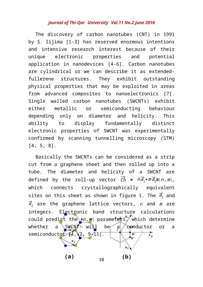
Basically the SWCNTs can be considered as a strip cut from a graphene sheet and then rolled up into a tube. The diameter and helicity of a SWCNT are defined by the roll-up vector Ch = n a1+m a2≡(n ,m), which connects crystallographically equivalent sites on this sheet as shown in figure 1. The a1 and a2 are the graphene lattice vectors, n and m are integers. Electronic band structure calculations could predict the (n , m) parameters, which determine whether a SWCNT will be a conductor or a semiconductor [4, 7, 9-11].
Figure 1: The hexagonal lattice and its Brillouin zone. (a) graphene lattice structure, made out of two interpenetrating triangular lattices which are a1and a2 are the lattice unit vectors, and δ i, i= 1, 2, 3 are the nearest-neighbour vectors. (b) represent the corresponding Brillouin zone. The Dirac cones are located at the K and K ' points [9].
There are three types of SWCNTs; first armchair carbon nanotubes which are always behaves as conductor, that is depend on n and m parameters (n=m), second one is zigzag carbon nanotubes which are exhibit as conductor and semiconductor depends on n parameter (m=0) and thirdly
37
Journal of Thi-Qar University Vol.11 No.2 June 2016
is the chiral carbon nanotubes, they are also behave as a conductor or semiconductor depend on m and n parameters (m≠n) [12, 13]. This means the behaviour of zigzag and chiral carbon nanotubes depends on the diameter of the nanotube [14].
It is well-known in the periodic table, that the III-V material most closely related to C is boron nitride (BN), which is like carbon, both of them have sp2- and sp3-bonded structures [15]. Boron nitride nanotube has a wide band Energy gap around Fermi energy which is approximately from 5.5 eV to 5.8 eV [15-17], this means all types of bulk boron nitride nanotubes are perfect insulator [15, 16, 18]. Many calculation reported that boron nitride nanotube energy gap is almost independent of tube diameter, chirality, and the number of tube walls [16, 17].
Hetero nanotubes received a huge interest from many scientists and research groups to understand their electronic properties and their possible applications [19-22], these studies reported that boron nitride has a remarkable effect on the energy gap of ideal carbon a nanotube. The importance of the interface between graphene and BN has been investigated [19, 23, 24], for these impurities, a characteristic peak close to the Fermi energy is found, with the peak associated with boron below the Fermi energy and the peak associated with nitrogen above the Fermi energy [19].
2. Theoretical Tools
The calculations are performed by using the SIESTA implementation of DFT [25] to find the optimized geometry. We followed the procedure explained in reference 27 and the ab-initio calculation was employed using the local density approximation (LDA) of the exchange and correlation functional with Ceperley-Alder exchange ‘CA’ parametrization, double zeta polarized (DZP) basis sets of pseudoatomic orbitals, a real-space grid defined with a plane-wave cutoff energy of 300 Ry and a maximum force tolerance of 10 meV/Å. The density of states (DOS) and electronic band structures (EBS) were calculated with 1×1×200 k-points. The Mean-Field Hamiltonian (MFH) obtained from SIESTA was used as an input data to calculate transmission coefficient T(E). to obtain the transmission coefficient
38

Journal of Thi-Qar University Vol.11 No.2 June 2016
T(E), we used the non-equilibrium Green’s function code GOLLUM [26] , which utilises the DFT-based hamiltonian from SIESTA. For ideal periodic structure, the number of open channels, is equivalent to the transmission coefficients T(E).
3. Electronic Properties of Ideal Nanotubes
In this section, we calculate the electronic properties of ideal carbon and boron nitride nanotubes to make sure that the used theoretical tools (SIESTA and GOLLUM codes) give the correct results. Figure 2 shows the supercell of the ideal carbon and boron nitride nanotubes.
Figure 2: Shows the ideal nanotubes (a) (10,10) carbon nanotube (360 carbon atoms), (b) (10,10) boron nitride nanotube (360 boron and nitrogen atoms).
Figure 2 shows the ideal conductor (10,10) carbon nanotube and ideal insulator (10,10) boron nitride nanotube that we obtained from SIESTA. The obtained results (figure 3) show good agreement with the publications which are reported that all sizes of armchair carbon nanotube are exhibiting a finite states at Fermi energy (conductors) and zero energy gap with two open channels at and around Fermi energy [12, 14]. Also, the boron nitride results confirmed that armchair boron nitride nanotube behaved as a perfect
39

Journal of Thi-Qar University Vol.11 No.2 June 2016
insulator with energy gap of approximately 4.5 eV, our result has a good agreement with the publications [15-18, 20]. Figure 3 show the results of ideal armchair carbon nanotube and boron nitride.
Figure 3: The electronic properties of the perfect carbon and boron nitride nanotubes. Figure2 (a-c) show the density of states (DOS), transmission coefficient T(E) and electronic band structure (EBS)of the ideal (10,10) carbon nanotube respectively. Figure2 (d-f) show the density of states (DOS), transmission coefficient T(E) and electronic band structure (EBS) of the ideal (10,10) boron nitride respectively. All calculations carried out with 1×1×200 k-points.
4. Electronic Properties of Hetero Nanotubes
40

Journal of Thi-Qar University Vol.11 No.2 June 2016
Here, we simulated the (10,10) hetero nanotubes with varying the hexagonal carbon rings (from one ring to four rings of carbon in between boron nitride rings) as shown in figure 4. By calculating the mean-field Hamiltonian (MFH) from SIESTA, we calculated the density of states (DOS) and the electronic band structures (EBS). Also, the obtained mean-field Hamiltonian (MFH) used to feed the GOLLUM code to investigate the transmission coefficient T(E). The calculations carried out with 1×1×200 k-points to make sure that the structures shown in figures (3a-3d) are periodic in Z direction and also to obtain the Van Hove singularity.
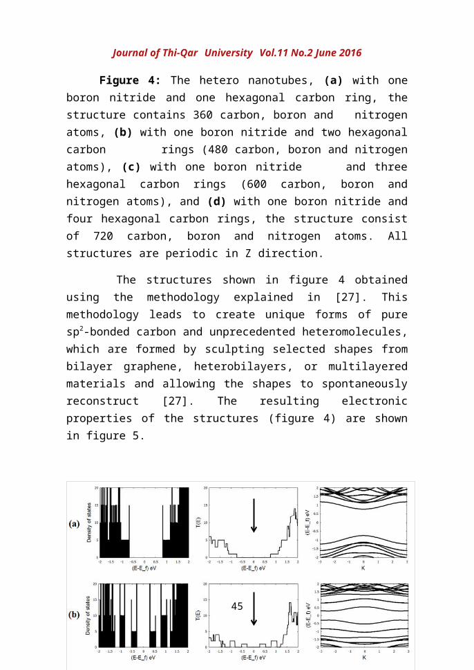
Figure 4: The hetero nanotubes, (a) with one boron nitride and one hexagonal carbon ring, the structure contains 360 carbon, boron and nitrogen atoms, (b) with one boron nitride and two hexagonal carbon rings (480 carbon, boron and nitrogen atoms), (c) with one boron nitride and three hexagonal carbon rings (600 carbon, boron and nitrogen atoms), and (d) with one boron nitride and four hexagonal carbon rings, the structure consist of 720 carbon, boron and nitrogen atoms. All structures are periodic in Z direction.
41

Journal of Thi-Qar University Vol.11 No.2 June 2016
The structures shown in figure 4 obtained using the methodology explained in [27]. This methodology leads to create unique forms of pure sp2-bonded carbon and unprecedented heteromolecules, which are formed by sculpting selected shapes from bilayer graphene, heterobilayers, or multilayered materials and allowing the shapes to spontaneously reconstruct [27]. The resulting electronic properties of the structures (figure 4) are shown in figure 5.
42

Journal of Thi-Qar University Vol.11 No.2 June 2016
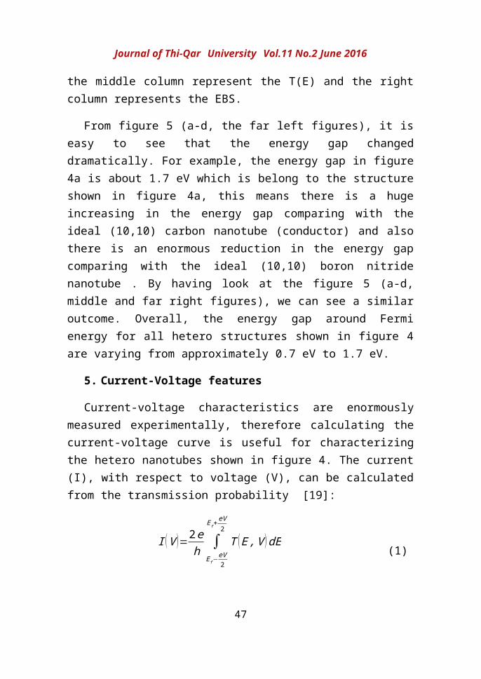
Figure 5: (a) the electronic properties of the structure shown in figure 3a, the density of states, transmission coefficient and band structure. (b) the density of states, transmission coefficient and band structure of the structure shown in figure 3b. (c) the density of states, transmission coefficient and band structure of the structure shown in figure 3c. (d) the density of states, transmission coefficient and band structure of the structure shown in figure 3d. In all figure a, b, c and d, the left column represents the DOS, the middle column represent the T(E) and the right column represents the EBS.
From figure 5 (a-d, the far left figures), it is easy to see that the energy gap changed dramatically. For example, the energy gap in figure 4a is about 1.7 eV which is belong to the structure shown in figure 4a, this means there is a huge increasing in the energy gap comparing with the ideal (10,10) carbon nanotube (conductor) and also there is an enormous reduction in the energy gap comparing with the ideal (10,10) boron nitride nanotube . By having look at the figure 5 (a-d, middle and far right figures), we can see a similar outcome. Overall, the energy gap around Fermi energy for all hetero structures shown in figure 4 are varying from approximately 0.7 eV to 1.7 eV.
5. Current-Voltage features
Current-voltage characteristics are enormously measured experimentally, therefore calculating the current-voltage curve is useful for characterizing the hetero nanotubes shown in figure 4. The current (I), with respect to voltage (V), can be calculated from the transmission probability [19]:
I (V )=2eh ∫
Ef −eV2
E f +eV2
T (E ,V ) dE (1)
From equation 1, we can see that the transmission depends on the bias voltage. The maximum current I(V) carried by the hetero nanotubes shown in figure 4 at a finite voltage V, is given by:
43

(a)(b)
(c)
(d)
Journal of Thi-Qar University Vol.11 No.2 June 2016
I (V )=2eh ∫
Ef −eV2
E f +eV2
T (E ) dE (2)
The resulting I-V plots for the optimized hetero nanotubes are shown in figure 5.
Figure 6: The obtained I(V) curve for (a) the hetero nanotube shown in figure 4a, (b) the hetero nanotube shown in figure 4b, (c) the hetero nanotube shown in figure 4c, and (d) the hetero nanotube presented in figure 4d.
Figure 6 shows clearly that at specific voltage value, for example at 0.8 volt the hetero structure with one hexagonal ring has the lowest current and the hetero structure with four hexagonal rings has the highest current. This result is due to the available states at and around the Fermi energy which means increasing the carbon rings layer will lead to enhance the conductance of the hetero nanotubes.
44
Journal of Thi-Qar University Vol.11 No.2 June 2016
6. Conclusions
In this work, the energy gap was manipulated of the hetero nanotubes from about 0.7 eV to 1.7 eV by varying the number of graphene rings from one ring to four rings in between the boron nitride rings. These values of the energy gap values are fall in the range of the semiconductors energy gap, for example the energy gap of silicon at room temperature is about 1.12 eV [28]. Boron nitride has non-trivial effect on the energy gap of carbon nanotube. In other word, doping the (10,10) carbon nanotube by boron nitride led to open the energy gap hugely. Also, increasing the graphene rings led to reduce and control the size of the energy gap of the hetero nanotubes. This is could be a good methodology to obtain a semiconductor with desirable band gap.
AcknowledgeI would like to thank Lancaster University/UK for allowing me to access the available facilities at the University through the Honorary Visiting that I obtained from Lancaster University. Also I would like to take this opportunity to express my gratitude to Prof. Colin J. Lambert and his group for their support to finish this work.
References
1. Lu, J.-Q., et al., Metal-to-semiconductor transition in squashed armchair carbon nanotubes. Physical review letters, 2003. 90(15): p. 156601.
2. Saito, R., G. Dresselhaus, and M.S. Dresselhaus, Physical properties of carbon nanotubes. Vol. 35. 1998: World Scientific.
3. Dresselhaus, M., G. Dresselhaus, and R. Saito, Physics of carbon nanotubes. Carbon, 1995. 33(7): p. 883-891.
4. Odom, T.W., et al., Atomic structure and electronic properties of single-walled carbon nanotubes. Nature, 1998. 391(6662): P. 62-64.
45

Journal of Thi-Qar University Vol.11 No.2 June 2016
5. Odom, T.W., et al., Structure and electronic properties of carbon nanotubes. The Journal of Physical Chemistry B, 2000. 104(13): p. 2794-2809.
6. Mintmire, J. and C. White, Electronic and structural properties of carbon nanotubes. Carbon, 1995. 33(7): p. 893-902.
7. X. Cao, J., et al., Electronic properties of single-walled carbon nanotubes. Journal of the Physical Society of Japan, 2002. 71(5): p. 1339-1345.
8. Wilder, J.W., et al., Electronic structure of atomically resolved carbon nanotubes. Nature, 1998. 391(6662): p. 59-62.
9. Neto, A.C., et al., The electronic properties of graphene. Reviews of modern physics, 2009. 81(1): p. 109.
10. Saito, R., et al., Electronic structure of chiral graphene tubules. Applied Physics Letters, 1992. 60(18): p. 2204-2206.
11. Hamada, N., S.-i. Sawada, and A. Oshiyama, New one-dimensional conductors: graphitic microtubules. Physical review letters, 1992. 68(10): p. 1579.
12. Tanaka, K., et al., Electronic properties of carbon nanotube. Chemical physics letters, 1994. 223(1): p. 65-68.
13. Ouyang, M., J.-L. Huang, and C.M. Lieber, Fundamental electronic properties and applications of single-walled carbon nanotubes. Accounts of chemical research, 2002. 35(12): p. 1018-1025.
14. Fischer, J.E. and A.T. Johnson, Electronic properties of carbon nanotubes. Current Opinion in Solid State and Materials Science, 1999. 4(1): p. 28-33.
15. Rubio, A., J.L. Corkill, and M.L. Cohen, Theory of graphitic boron nitride nanotubes. Physical Review B, 1994. 49(7): p. 5081.
16. Chopra, N.G., et al., Boron nitride nanotubes. science, 1995. 269(5226): p. 966-967.
17. Blase, X., et al., Stability and band gap constancy of boron nitride nanotubes. EPL (Europhysics Letters), 1994. 28(5): p. 335.
18. Golberg, D., et al., Boron nitride nanotubes and nanosheets. Acs Nano, 2010. 4(6): p. 2979-2993.
19. Algharagholy, L., et al., Electronic properties of sculpturenes. New Journal of Physics, 2014. 16(1): p. 013060.
46
Journal of Thi-Qar University Vol.11 No.2 June 2016
20. Pan, H., Y.P. Feng, and J. Lin, Boron nitride and carbon double-wall hetero-nanotubes: first-principles calculation of electronic properties. Nanotechnology, 2008. 19(9): p. 095707.
21. Majidi, R., K.G. Tabrizi, and S. Jalili, Effect of doping on electronic properties of double-walled carbon and boron nitride hetero-nanotubes. Physica B: Condensed Matter, 2009. 404(20): p. 3417-3420.
22. Wei, X., et al., Electron-beam-induced substitutional carbon doping of boron nitride nanosheets, nanoribbons, and nanotubes. Acs Nano, 2011. 5(4): p. 2916-2922.
23. Charlier, J.-C., Defects in carbon nanotubes. Accounts of chemical research, 2002. 35(12): p. 1063-1069.
24. Wiggins-Camacho, J.D. and K.J. Stevenson, Effect of nitrogen concentration on capacitance, density of states, electronic conductivity, and morphology of N-doped carbon nanotube electrodes. The Journal of Physical Chemistry C, 2009. 113(44): p. 19082-19090.
25. Soler, J.M., et al., The SIESTA method for ab initio order-N materials simulation. Journal of Physics: Condensed Matter, 2002. 14(11): p. 2745.
26. Ferrer, J., et al., GOLLUM: a next-generation simulation tool for electron, thermal and spin transport. New Journal of Physics, 2014. 16(9): p. 093029.
27. Algharagholy, L., et al., Sculpting molecular structures from bilayer graphene and other materials. Physical Review B, 2012. 86(7): p. 075427.
28. Luppi, M. and S. Ossicini, Ab initio study on oxidized silicon clusters and silicon nanocrystals embedded in Si O 2: Beyond the quantum confinement effect. Physical Review B, 2005. 71(3): p. 035340.
47

Journal of Thi-Qar University Vol.11 No.2 June 2016
48