fpga implementation of adaptive filter
TRANSCRIPT

BYMD.SHIFAT ISLAM TALUKDER
4226267
FPGA Implementation of Adaptive Filter
Learning Objectives
Introduction to adaptive filtering
LMS algorithm
Implementation of LMS algorithm on FPGA
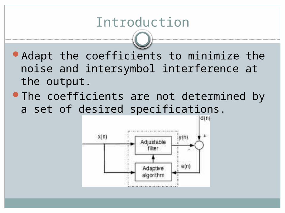
Introduction
Adapt the coefficients to minimize the noise and intersymbol interference at the output.
The coefficients are not determined by a set of desired specifications.
Introduction
An alternative method of estimating a signal corrupted by noise or interferences.
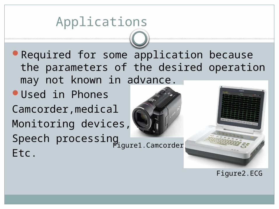
Applications
Required for some application because the parameters of the desired operation may not known in advance.
Used in PhonesCamcorder,medical Monitoring devices,Speech processing Etc.
Figure2.ECG
Figure1.Camcorder
Criteria
Designing the processing system(ASIC,DSP,FPGA etc.)
Which algorithm to use to update the coefficient of the selected filter(LMS,RLS).
Feasibility of implementationPerformanceCost
Processing System
DSP is suited for complex math intensive task but have problem with high sampling rate application.
ASIC lacks flexibility and require long design cycle
FPGA is the best option in terms of flexiblity, cost, and performance.
LMS algorithm
Least mean squares (LMS) algorithms are a class of adaptive filter used to mimic a desired filter by finding the filter coefficients that relate to producing the least mean squares of the error signal (difference between the desired and the actual signal).
Presented by Widrow and Stearns in 1985[1].
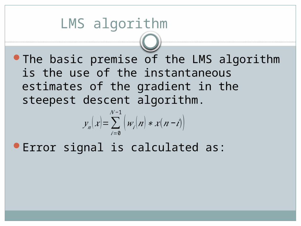
LMS algorithm
The basic premise of the LMS algorithm is the use of the instantaneous estimates of the gradient in the steepest descent algorithm.
Error signal is calculated as:𝑦 𝑛 (𝑥 )=∑
𝑖=0
𝑁− 1
(𝑤𝑖 (𝑛 )∗𝑥 (𝑛−𝑖))

LMS algorithm
Finally the weight coefficient is updated(n+1)=Where µ=is the step size parameter
Variable Filter
Update algorithm
+
x(n)
y(n)d(n)
w(n)
e(n)
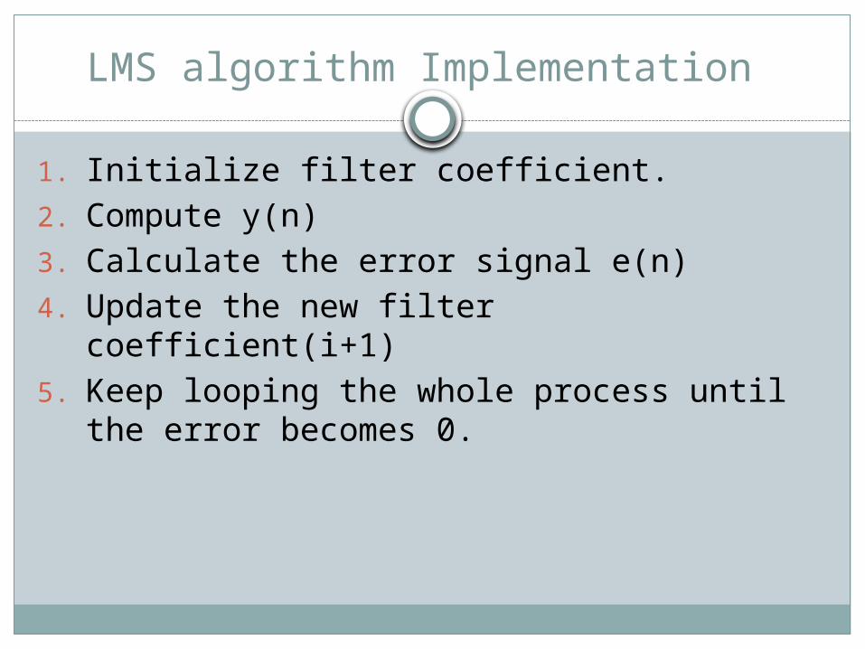
LMS algorithm Implementation
1. Initialize filter coefficient.2. Compute y(n)3. Calculate the error signal e(n)4. Update the new filter coefficient(i+1)5. Keep looping the whole process until the
error becomes 0.
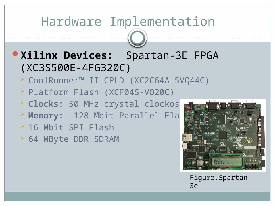
Hardware Implementation
Xilinx Devices: Spartan-3E FPGA (XC3S500E-4FG320C) CoolRunner™-II CPLD (XC2C64A-5VQ44C) Platform Flash (XCF04S-VO20C) Clocks: 50 MHz crystal clockoscillator Memory: 128 Mbit Parallel Flash 16 Mbit SPI Flash 64 MByte DDR SDRAM
Figure.Spartan 3e
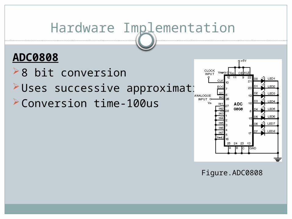
Hardware Implementation
ADC08088 bit conversionUses successive approximationConversion time-100us
Figure.ADC0808
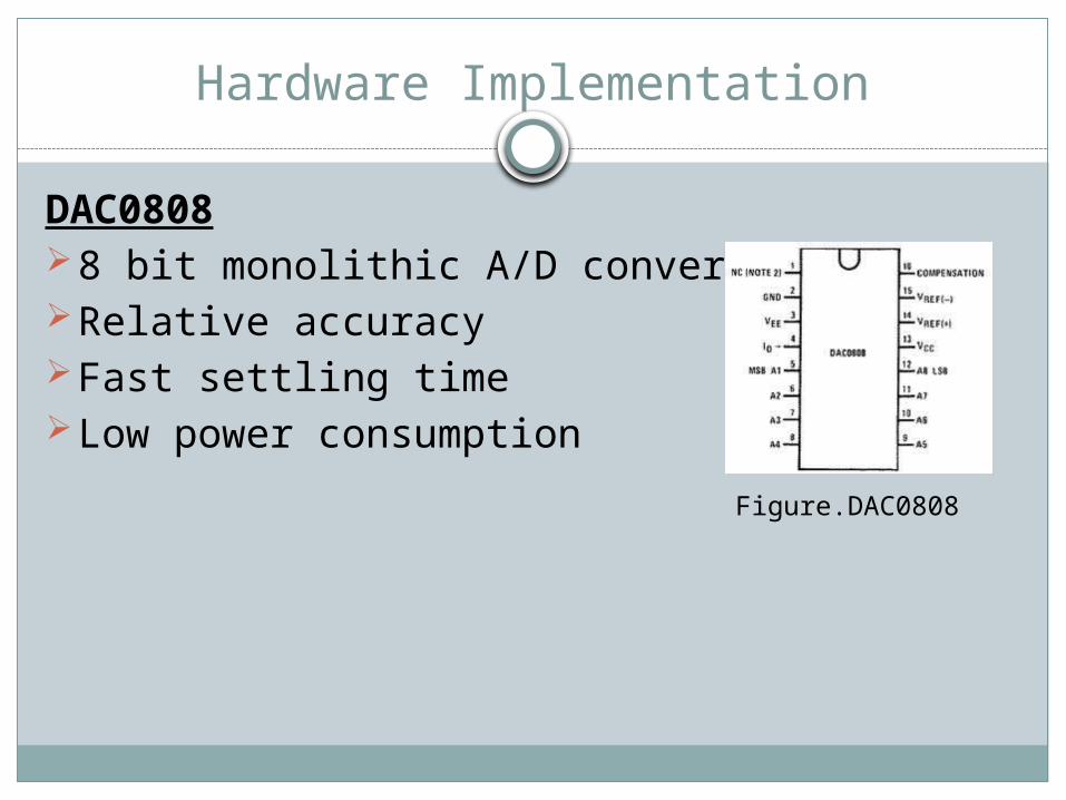
Hardware Implementation
DAC08088 bit monolithic A/D converterRelative accuracyFast settling timeLow power consumption
Figure.DAC0808
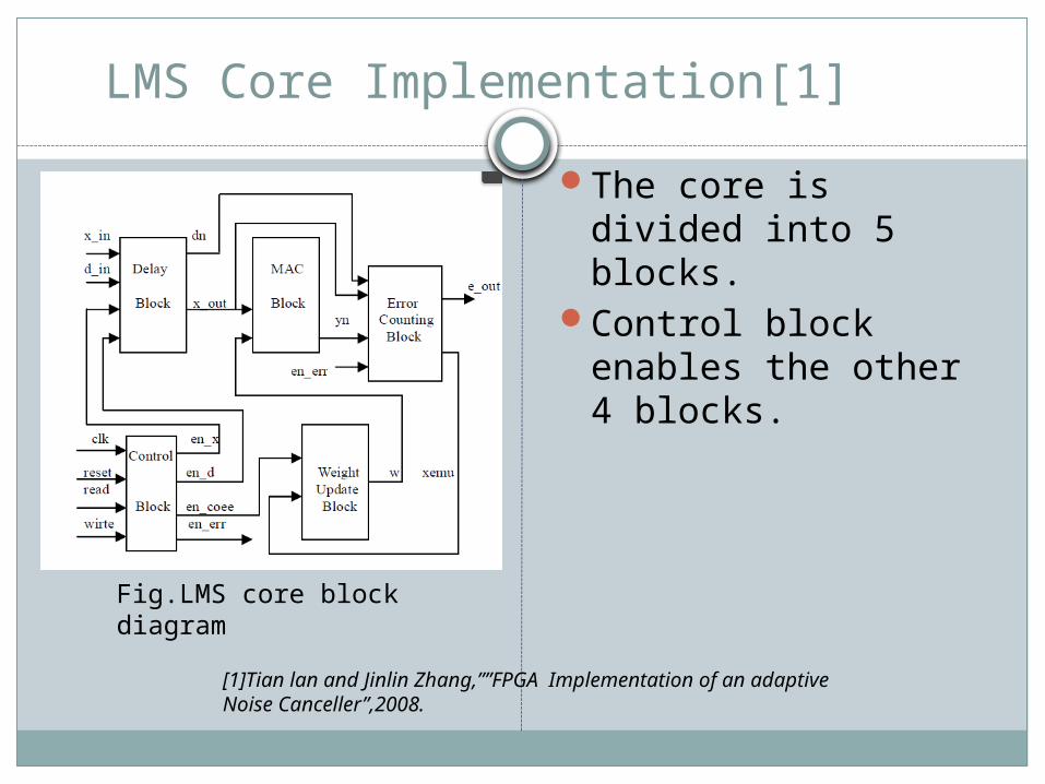
LMS Core Implementation[1]
The core is divided into 5 blocks.
Control block enables the other 4 blocks.
Fig.LMS core block diagram
[1]Tian lan and Jinlin Zhang,””FPGA Implementation of an adaptive Noise Canceller”,2008.

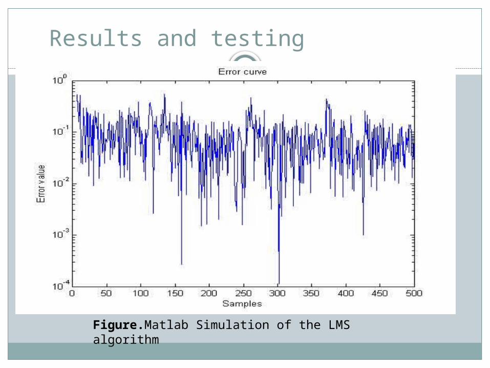
Results and testing
Figure.Matlab Simulation of the LMS algorithm
Results and testing
Figure.Matlab Simulation of the LMS algorithm

Future Work
Simulation of adaptive filter.Implementation of LMS on FPGA.Troubleshooting, TestingLiterature review of RLS algorithm.Simulation and Implementation of RLS on
FPGAComparison of the 2 algorithm based on
accuracy, cost, time and performance.
Conclusion
Various method of implementing Adaptive filtering have been studied.
LMS and RLS are the most preferred choice.Implementation of both LMS and RLS will be
achieved by the end of the next semester.
Thank you