fine resolution radar for near-surface layer mapping · pdf file · 2004-12-06fine...
TRANSCRIPT

University of Kansas
1
Fine Resolution Radar for Near-Surface Layer Mapping
Master’s Thesis Defense
Rohit ParthasarathyDate: August 25th, 2004
CommitteeDr. Sivaprasad Gogineni (chair)Dr. Christopher AllenDr. Glenn Prescott

University of Kansas
2
OutlineIntroductionBackgroundDesign ConsiderationsSystem DesignExperiments and Results Conclusions and Recommendations

University of Kansas
3
IntroductionEarth’s average temperature has risen about 1.8 °F over the last century
Ocean conditions are a significant indicator of global climate change
Sea level has risen between 4 to 8 inches over last century
If temperatures continue to rise, polar ice caps could melt, which will have a huge impact on coastal areas

University of Kansas
4
IntroductionIf the entire Greenland ice cap were to melt, sea levels would rise by 7 m,
displacing a large population
Even a 1 m rise could submerge a few cities in Bangladesh
Uncertainty over what role the ice sheets play in the rising sea level
A key parameter in assessing ice sheets contribution is the mass balance
Precise measurements of mass balance needed to reduce the uncertainty of ice sheet contribution
Key parameter in assessing mass balance is knowledge of the accumulation rate

University of Kansas
5
Introduction• To estimate accumulation rate, remote sensing techniques are valuable
• Such techniques help reduce the spatial and temporal uncertainty that currently exists due to sparse sampling
• We developed a wide-band FM-CW radar to map the near-surface internal layers to a depth of 150 to 200 m with 10 cm resolution

University of Kansas
6
Background-PRISM Project PRISM Project was undertaken through a large grant from NASA and NSF
Multidisciplinary Group was assembled to develop radars, rovers, intelligent systems, and communication systems. Goal is to develop an autonomous sensor web. 3 sensors are SAR, Depth Sounder, Accumulation Radar
Goals for the Accumulation Radar include:
Generation of extremely linear chirp signal
Achieving a fast sweep rate
Mapping internal layers to a depth of 150 to 200 m with 10 cm resolution
Housing the entire radar in one CompactPCI chassis

University of Kansas
7
FM-CW BackgroundIn FM-CW radar, a chirp signal is transmitted, hits a target, and is mixed with the transmit signal. If many targets are present, the IF signal will be a superposition of many signals at different beat frequencies The beat frequency is Bτ/T, and the resolution is c/2B.

University of Kansas
8
FM-CW BackgroundIf the amplitude of the transmit signal is not perfectly flat, sidebands will appear in the beat spectrum. If the amplitude signal is modulated by cos(fm*t), the sidebands will be +/- fm away from the main signal
If the phase of the transmit signal is not perfectly quadratic, sidebands will also appear in the beat spectrum.
University of Kansas
9
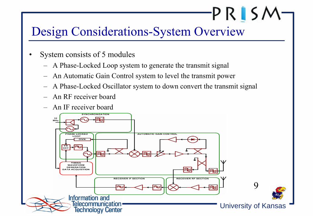
Design Considerations-System Overview
• System consists of 5 modules– A Phase-Locked Loop system to generate the transmit signal – An Automatic Gain Control system to level the transmit power – A Phase-Locked Oscillator system to down convert the transmit signal – An RF receiver board – An IF receiver board

University of Kansas
10
Design Considerations-System Specifications
We used a 12-bit A/D converter
Its dynamic range is 74 dB, the power of the maximum signal which can be digitized is 4 dBm, and the noise floor is –70 dB
The noise floor of the radar system is given by: N = kTBF, where B is the bandwidth of one range bin = sampling rate/number of DFT points = 10 MHz/40,000 = 250 Hz.

University of Kansas
11
Design Considerations-System Specifications
Noise Figure of the receiver given by the following formula:
∏−
=
−+
−+
−+= 1
1
21
3
1
21
1...
11N
nn
N
G
FGG
FG
FFF
The Noise Figure of the front end of the receiver is approximately 9 dB
Plugging these numbers in results in a MDS of –140 dB.
University of Kansas
12
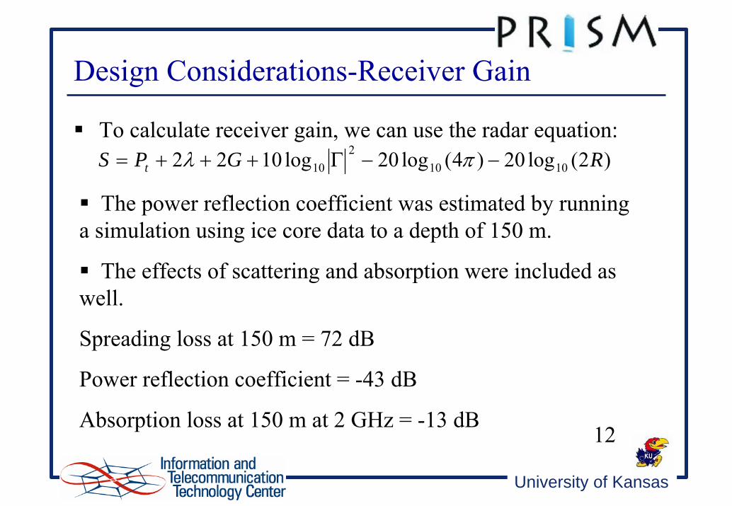
Design Considerations-Receiver Gain
To calculate receiver gain, we can use the radar equation: )2(log20)4(log20log1022 1010
210 RGPS t −−Γ+++= πλ
The power reflection coefficient was estimated by running a simulation using ice core data to a depth of 150 m.
The effects of scattering and absorption were included as well.
Spreading loss at 150 m = 72 dB
Power reflection coefficient = -43 dB
Absorption loss at 150 m at 2 GHz = -13 dB

University of Kansas
13
Design Considerations-Receiver Gain
Plugging these values in the previous formula, we find that the expected return power at 150 m at a frequency of 2 GHz is –138 dBm
We need to set the receiver gain such that the weakest signal is brought above the A/D noise floor.
SNRFloorNoiseDAGIntGainSP RCRT +>+++ /
We assume a SNR of 10 dB and 10 coherent integrations. Then,
the gain should be greater than 44 dB

University of Kansas
14
Design Considerations-System Parameters
Frequency (MHz): 500 to 2000 Sweep Time (ms): 4 Transmit Power (dBm): 20Antenna Type: TEM Horn A/D Dynamic Range: 12-bit 72 dB

University of Kansas
15
Design Considerations-PLL overview
PLL system uses YIG oscillator to generate transmit signal YIG has two coils, main coil which has a large frequency sensitivity, but a relatively small BW, and an FM coil, which has a small frequency sensitivity, but larger BWPrevious FM-CW systems used a YIG oscillator in a PLL configuration, but used only the main coil to phase lock it. This limits the sweep time We apply a ramp voltage to the main coil, which generates a 4.5 to 6 GHz signal, and use a PLL to phase lock it to a low-frequency chirp. We use the FM coil in the feedback loop to phase lock the signal. It is possible to achieve excellent linearity with fast sweep rates

University of Kansas
16
Design Considerations-PLL
Block Diagram of PLL System
University of Kansas
17
Design Considerations: Automatic Gain Control
Automatic Gain Control (AGC) is required to level the transmitpower off, since variations in transmit power will result in unwanted sidebands.
The AGC system consists of a front-end stage to down convert the YIG signal from 4.5-to-6 GHz to 500-to-2000 MHz. We used a high frequency YIG because it could be swept faster and the harmonics were out of band.
After down conversion, the signal goes through an amplifier stage, so that we are transmitting the correct power. The first amplifier is a VGA.
Before transmitting, a portion of the power is fed-back, converted to a voltage, conditioned and filtered, and used to control the VGA’s gain.

University of Kansas
18
Design Considerations-AGC
Diagram of the AGC System

University of Kansas
19
Design Considerations: Phase-Locked Oscillator
The purpose of the PLO section is to generate a 4 GHz signal and a 50 MHz signal. The 4 GHz signal is used to down-convert the YIG signal from 4.5-to-6 GHz to 500-to-2000 MHz. The 50 MHz signal is used to drive the data acquisition system.
Diagram of the PLO System

University of Kansas
20
Design Considerations: Receiver RF System
The purpose of the RF system is to filter and amplify the received signal and mix it with the transmit signal for down-conversion
We need to make sure that the power going into the RF port of the mixer is at least 15 dB below the power going into the LO port. This minimizes the effect of third order products.
Diagram of the RF System

University of Kansas
21
Design Consideration: IF SectionThe purpose of the IF section is to provide any required amplification to the down-converted signal. Also, a high-pass filter is used to filter out the antenna feed-through, and a low-pass filter prepares the signal to be digitized.
The high-pass filter is a Gaussian Filter, which minimizes ringing and transient effects. It attenuates the feed-through signal and returns from the top-layers, since these can saturate the A/D converter.

University of Kansas
22
System Design: PLL
The main circuits in the PLL system are the main coil driver, the FM coil driver, and the loop filter
The YIG coils are inductors, and the YIG sphere requires a magnetic field to tune it. By passing current through the inductor, a magnetic field is generated.
The main coil driver takes an input voltage and converts it into a current to drive the main coil. The FM driver drives the FM coil
The loop filter filters the error signal from the PLL.

University of Kansas
23
System Design: Main Coil Driver
Important to minimize noise, since even small amounts of noise can cause large frequency deviations.
Input voltage is between –1 and 1 V.

University of Kansas
24
System Design: FM Coil Driver
Built a differential driver. Needed to be able to generate +/-100 mA, which is more than enough to correct for any deviation

University of Kansas
25
System Design: Loop Filter
Loop filter take charge pump current and filters it and converts it into a voltage
Loop filter BW set to 30 kHz, which is wider than main coil driver circuit. Loop filter should be able to pass the error signal required to lock the YIG

University of Kansas
26
System Design: PLL and Oscillator Tests
Loop Filter Voltage vs. Time

University of Kansas
27
System Design: PLL and Oscillator Tests
Unlocked Oscillator (Red) vs. Locked Oscillator (Blue)

University of Kansas
28
System Design: PLL and Oscillator Tests
We performed noise analysis on the main coil driver circuit, and found en = 2*10^-6. We developed a model for phase noise of an unlocked oscillator using narrowband FM approximation, and fit a curve to the locked oscillator:
The value for en here is 7.15*10^_8. In either case, the sidebands due to phase noise will be more than 30 dB down

University of Kansas
29
System Design: PLL Board
PLL Board

University of Kansas
30
System Design: AGC
The AGC consists of a down-conversion stage followed by an amplifier stage, and a low-frequency circuit for feed-back
We need to determine how much open-loop gain variation there is to decide where to operate the VGA at.

University of Kansas
31
System Design: AGC Open Loop Gain
m1freq=dB(S(2,1))=34.518
500.1MHzm2freq=dB(S(2,1))=25.574
2.000GHz
0.6 0.8 1.0 1.2 1.4 1.6 1.8 2.0 2.20.4 2.4
25
30
35
20
40
freq, GHz
dB(S
(2,1
))
m1
m2

University of Kansas
32
System Design: Low Frequency Feed-Back Circuit
After determining where to set the VGA voltage, we used a potentiometer to shift the level of the VGA signal to get to the right spot

University of Kansas
33
System Design: AGC Results
VGA Voltage vs. Time

University of Kansas
34
System Design: AGC Results
0.6 0.8 1.0 1.2 1.4 1.6 1.8 2.0 2.2 2.40.4 2.6
14
15
16
17
18
19
13
20
freq, GHz
TRA
NS
MIT
..Tra
ceA
Variation in Transmit Power

University of Kansas
35
System Design: AGC Boards
AGC Low Frequency Plug-On Board
High Frequency AGC Board

University of Kansas
36
System Design: PLOWe needed to generate a 4 GHz and 50 MHz signal locked to a 10 MHz rubidium source. We purchased off-the-shelf PLO
chips from Synergy.
PLO Board

University of Kansas
37
System Design: RF System
We designed this system assuming that the transmit and receive antennas would be on opposite sides of the tracked vehicle. In that case, the feed-through signal was estimated to be at –30 dBm.
We set the gain of this stage based on this expected power, assuming the LO power to the mixer would be 7 dBm
We used a high-reverse isolation amplifier to ensure that little power would leak through and be retransmitted
RF System

University of Kansas
38
System Design: RF Board
RF Board

University of Kansas
39
System Design: IF System
The frequency of the feed-through signal was calculated to be 9 kHz. We put 75 dB of attenuation at that frequency. We used a high-speed op-amp to amplify the signal to the appropriate level. We then filtered the signal before it goes to the A/D converter
IF System

University of Kansas
40
System Design: IF Board
IF Board

University of Kansas
41
Experiments and Results: NGRIP
We developed a prototype system which was tested in NGRIP during the summer of 2003.

University of Kansas
42
Experiments and Results: NGRIP
Fading due to sweep time, number of coherent integrations, and antenna movement.
Water Equivalent Accumulation Rate: 18 cm/year, close to estimates of 17 cm/year
University of Kansas
43
Experiments and Results: System Improvements
After testing the prototype radar, we noticed several areas thatcould be improved
We built lower-noise driver circuits
We widened the loop filter bandwidth
We improved the AGC circuit to minimize power fluctuations
We reduced the size of the radar significantly, so that it fits in one CompactPCI chassis

University of Kansas
44
Experiments and Results: Operational Radar

University of Kansas
45
Experiments and Results: Delay Line Tests
We performed several delay-line tests with this system.
Uncorrected Response (Red) vs. System Effects (Blue)

University of Kansas
46
Experiments and Results: Delay Line Tests
To isolate the problem, we did a delay-line test with the YIG only.
Delay Line Result with Oscillator Only

University of Kansas
47
Experiments and Results: Delay Line Tests
We removed the delay line effects and the system effects.
Corrected Spectrum (Blue) vs. Ideal Spectrum (Red)

University of Kansas
48
Experiments and Results: Summit Results
We tested the radar during the 2004 field season at Summit camp, Greenland

University of Kansas
49
Experiments and Results: Summit Results
Calculated vs. Simulated Reflection Coefficient
Water Equivalent Accumulation Rate is estimated to be .36 m which is similar to estimates of .3 m.

University of Kansas
50
Conclusions
Designed and developed a compact FM-CW Radar
Fast sweep chirp signal
FM coil used to phase-lock YIG
Successfully mapped the internal layers at NGRIP and Summit with high resolution to a depth of 200 m

University of Kansas
51
Recommendations
For airborne applications, we need a faster sweep. This will require optimizing loop filter and drivers to accommodate faster sweeps.

University of Kansas
52
Questions?