:final report - defense technical information center · microwave active network synthesis final...
TRANSCRIPT
AD
Research and Development Technical ReportECOM-0044-F
MICROWAVE ACTIVE: NETWORK SYNTHESIS
:FINAL REPORT0
E. G. Crista/ A. Pade/I S. B. Cohn_ 0
1FEBRUARY 1972 .0!
* DISTRIBUTION STATEMENT
Approved for Public Release; Distribution Unlimited.
ECOMUNITED STATES ARMY ELECTRONICS COMMAND FORT MONMOUTH, N.J. 07703
CONTRACT DAAB07-70-C-0044 Reproducd by 4STANFORD RESEARCH INSTITUTE NATIONAL TECHNICAL 1IN4FORMATION SERVICEF
Menlo Park, California 94025 I ,o A O SERVICE
Spf 7i_.V, 25

NOTICES
Disclaimers
The findings in this report are not :o be construed as an officialDepartment of the Army position, unless so designated by otherauthorized documents.
The citation of trade names and names of manufacturers in this reportis not to be construed as official Government indorsement or approvalof commercial products or services referenced herein.
Disposition
Destroy this report when it is no longer needed. Do not return it tothe originator.
A t
-- •=~ -v~~ ~--

r7 -
TECHNICAL REPORT ECOM-0044-F Reports Control SymbolOSD-1366
FEBRUARY 1972
MICROWAVE ACTIVE NETWORK SYNTHESIS
FINAL REPORT
SRI Project 8245
CONTRACT DAABO7-70-C-0044
?E- Prepared by
E. G. CRlISTAL A.PODELL S. B. COHN
STANFORD RESEARCH INSTITUTE
MENLO PARK, CALIFORNIA 94025
For
U.S. ARMY ELECTRONICS COMMAND, FORT MONMOUTH, N.J. 07703
DISTRIBUTION STATEMENT
Approved for Public r~eease; Distribution Unlimited.
Detais 01illustrations InL thig document may be bettVr
tuedon microfiche

ABSTRACT
This repoet describes the application of meander lines to impedance
transformers, and discusses two types of negative-impedance circuits and
two slot-line topics.
It is demonstrated that meander lines constitute a class of imped-
ance transformers of which stepped-mpedance transformers are a speeiai
case. A design table is presented for nearly-equal-ripple meander-line
transformers of from 2 to 6 turns, incorporating a wide range of band-
widths and impedance transformations. Experimental confirmation of the
aesign table is given.
Two types of negative-impedance-converter (NIC) circuits were
designed and constructed: (1) a high-power NUNIC, and (2) a FET-NIC
filter. A high-power NUNIC circuit intended for operation at 200 to
500 MHz was built and produced negative resistance from below 80 MHz
to above 680 MHz. A lossless one-pole filter incorporating the NUNIC
was built for operation at 230 MHz and exhibited a 3-dB filter bandwidth
of 2.7 MHz. Tne 1-dB compression point occurred at 1 watt of iizput
power (+30 dBm) and the third-order intermodulation intercept measured
+34.5 dB. A FET-NIC filter has been constructed in microwave integrated
circuit (MIC) form. It was possible to vary the bandwidth of this filter
electrically over a 7:1 range. The size of the complete MIC FET-NIC
filter is comparable with a small power-transistor package, approximately
z1/2 inch square by 1/16 inch high.
rThe slot-line tcpics treated are, firstly, symmetrical four-layer-
sandwich slot line, which is discussed for ferrite-phase-shifter appli-
cations. Formulas are given for wavelength, characteristic impedance,
~ili

and magnetic-field-strength distribution. Curves of the latter are
helpful for phase-shifter optimization. Secondly, coupling between
two parallel slot lines is analyzed, and a few typical curves of
coupling and directivity versus frequency are shown.
iv
PURPOSE OF CONTRACT
The purpose of this contract is to develop techniques for the
design of passive and active filte-s and components in the VHF-to-
microwave-frequency range, and to determine the electromagnetic
properties of slot line for integration with microstrip technology.
V
_
L

CONTENTS
ABSTRACT . .iii .........
PURPOSE OF CNTRACT,....... ................... v
LIST OF ILLUSTRATIONS. .. ....................... ix
-= ~~LIST OF TABLES.............................................xi
= ACKOWLEDGMENTS. ........ .. .................
I INTRODUCTION......................... . . . ... . .. .. .. ........
A. Meander-Line and Hybrid Meander-Line Transformers. .
B. Negative-Impedance Converters.... .. .. ...........
C. Slot Line .. ........................ 2
11 MEANDER-LINE AND HYBRID MEANDER-LINE TRANSFORMERS. ....... 3
A. General. ............ .............. 3
=B. Meander-Line-Transformer Design Tables . . . . .. .. .. 7
1.* Definition of Parameters Used in Design Tables . 8
2. Discussion of Design Tables. .. ............ 36
3. Example Design. .................. 40
C. Experimental Results .. ....... ........... 41
1. Three-Turn4leander-Line Transformer .. .. ...... 41
2. Fourth-Order Hybrid Meander-Line Transformer . . . 43
III NEGATIVE-IMPEDANCE CONVERTERS. ........... ..... 49
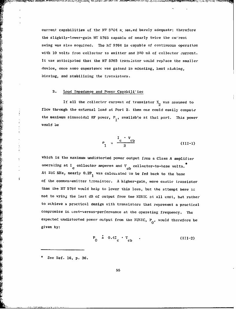
A.* General . . . . . . . .. .. .. .. .. .. .. .... 49
B. The NT.NIC Circuit. ............ .. . . . . 49
1. Qualitative Analysis .. ................ 49
2. Choosing Transistors. ...... .......... 54
3. Load Impedance and Power Capabilities. .. ...... 55
vii

4. NINIC Load and Emitter Impedances . . ...... 585. NUNIC Measurements. ................. 60
6. Noise Figure ........ .................... ... 60
7. Circuit Modifications .... ........... . . . 61
C. The Integrated FET-NIC .... ................. .. 63
1. Circuit Design........... . . . . . . . . 63
2. Circuit Redesign ....... .................. ... 68
D. Final Results ........ ..................... .. 71
IV SIOT LINE .......... .......................... 73
A. General .......... ......................... ... 73
B. Multilayer Sandwich Slot Line .... .......... . . . 75
C. Coupling Between Slot Lines ... ........... . . .. 85
V CONCLUSIONS ... ........... ....... . . . . . . 91
A. Meander-Line and Hybrid Meander-Line Transformers.. . 91
B. Negative-impedance Converters ..... .............. ... 91
C. Slot Line .......... ....................... ... 92
REFERENCES ............. ............................ ... 93
DISTRIBUTION LIST .......... ......................... ... 97
DD Form 1473
viii

ILLUSTRATIONS
Figure 1I-i Stepped-Impedance Transformer 4........... 4
Figure 11-2 Conventional Meander-Line Geometries ............ 5
Figure 11-3 Hybrid Meander-Line Geometries .. .. .......... 6
Figure 11-4 Two-Port Equivalent Circuits for Meander Lines
Having Negligible Coupling Between Nonadjacent
Turns ........... ....................... 7
Figure 11-5 Schematic Cross-Sectional Representation for
Meander-Line Transformers ....... ............ 8
Figure 11-6 Variation of Feak VSWR for Various Coupling
Values Between Meapder-Line Turns .......... ... 37
Figure 11-7 VSWR vs. Electrical Degrees for N = 3-, 4-, and
5-Turn Meander-Line Transformers ............ .. 38
Figure I-8 VSWR vs. Bandwidth for Meander-Line and
Stepped-Impedance Transformers ............. ... 40
Figure 11-9 Photograph of Experimental Three-Turn-Meander-
Line Transformer. . ..... ................ ... 44
Figure II-10 Measured and Computed VSW1s for Experimental
Three-Turn-Meander-Line Transformer ......... ... 45
Figure 1I-11 Measured Reflection Coefficient on a Smith-Chart
Overlay for the Experimental Three-Turn-leander-
Line Transformer ..... ............... . . . 46
Figure 11-12 Photograph of an Experimental N = 4 Hybrid
Meander-Line Transformer .... .............. ... 47
Figure 11-13 Measured and Computed Return Loss for Experimental
N = 4 Hybrid Meander-Line Transformer ......... ... 48
Figure III-1 NUNIC with Negative Feedback ... ............ ... 50
Figure 111-2 Phase and Amplitude of 5 and $ + 1 .......... . 53
Figure 111-3 Modified NUNIC Circuits .... ........... ... 62
Figure 111-4 Schematic Diagram of First Integrated
FET-NIC Filter ...... ................... .... 64
ix

-MIT
Figure 111-5 Photograph of MIC Realization of
FET-NIC Filter ...... ................... ... 65
Figure III-6 Equivalent Circuit of FET-NIC .............. .... 67
Figure 111-7 Schematic Diagram and Substrate Layout
of Second Integrated FET-NIC Filter ........... ... 69
Figure IV-l Slot Line on a Dielectric Substrate ........... .. 74
Figure IV-2 Sandwizh-Slot-Line Cross Section with a Pair
of Electric or Magnetic Walls ... ........... .... 74
Figure IV-3 Symmetrical Multilayer-Sandwich Slot Line ... ...... 76
Figure IV-4 Fields H and H /j vs. z in y = 0 Plane,z x
- 9.6 ....... ..................... ... 83rl
Figure IV-5 Fields H and H /j vs. z in y = 0 Plane,
£ = 30 ............. ............ ... 84rl . . . . .
Figure IV-6 Basic Slot-Line Cross Section, Equivalent
Infinite Arrays, and Coupled Slot Pair ....... ... 86
Figure IV-7 Equivalent Circuit of Coupled Slot Lines ..... .. 88
Figure IV-8 Coupling and Directivity vs. Frequency for
a Pair of Coupled Slots .... ............... .... 89
x

TABLES
Table 11-1 Meander-Line-Transformer Designs .. .......... 10
Table 11-2 Examll Four-Turn-Meander-Line3:1-Bandwidth Transformer Design (RL/RG; 2) . . . . 42
Table 11-3 Electrical and Dimensional Parameters for an
Experimental Stripli e Three-Turn-3.eander-
-- Line Transformer. ................ ... 42
Table 11-4 Electrical and Dimensional Parameters for an
Experimental Fourth-Order Stripline HybridMeander-Line Transformer .. ............... 47
Table 111-1 Final Element Values .. ................. 59
Table 111-2 Conductance Change with f Variation .. ......... 59
Table 111-3 NIC Filter Performance..................71
xi

ACKNOWLEDGMENTS
The ruthors are indebted to Dr. Ulrich Gysel for numerous illumi-
nating discussions concerning the numerical methods used to obtain the
meander-line design table, and for allowing the authors the use of
h~s modiiied computer program of the Fletcher-Powell technique for
minimization of a function of several variables. The use of this
program undoubtedly saved considerable computer time in compiling the
design table. The authors would also likE to ackrgwledge the excellent
work donc- by Mr. Eldon Fernandes of SRI, who accurately constructed
and measured the eyperimental meander-line transformers.
xiii

I INTRODUCT ION
A. Meander-Line and Hybrid Meandr-Line Transformers
In Section II the application of meander lines to impedance trans-
formers is proposed and developed. Meinder-line transformers have
less bandwidth than stepped-impedance transformers for a given passband
VSWR, but can have greatly superior shape factors in stripline and MIC
realizations. Hybrid meander-line transformers allow circuit designers
greatly increased flexibility in choosing transformer shape factors,
while allowing (basically) the same electrical performance as with
either stepped-impedance or meander-line transformers. A comprehensive
meander-line-transformer-design table is presented in Section II.
B. Negative-Impedance Converters
Work on the NIC circuit (luring the past reporting period was con-
ducted in the following areas: (1) increasing the power-handling capa-
bilities of the NIC, (2) increasing its flexibility of application, and
(3) decreasing its size. The progress that was made in all three of
these areas is described in Section III. In particular, a 1-watt UHF
NIC filter was constructed and an integrated-circuit FET-NIC filter was
built with electronically variable bandwidth. These circuits were shown
to be insensitive to both device-parameter variations and environmental
changes.

P 7MMM1 2. 7U77
C. Slot Line
The investigation of slot line is brought to a close in Section IV
of this report. One final subject is the symmetrical four-layer-sandwich
slot line, which is being applied to ferrite phase shifting in another
USAECOM program. Formulas of wavelength, characteristic impedance, and
magnetic-field distribution are given. Field computations and plots
are useful in selecting parameters for good phase-shifter performance.
A second subject is analysis of directional coupling of a pair of slots.
Directivity and coupling versus frequency are shown graphically for
several cases.
2
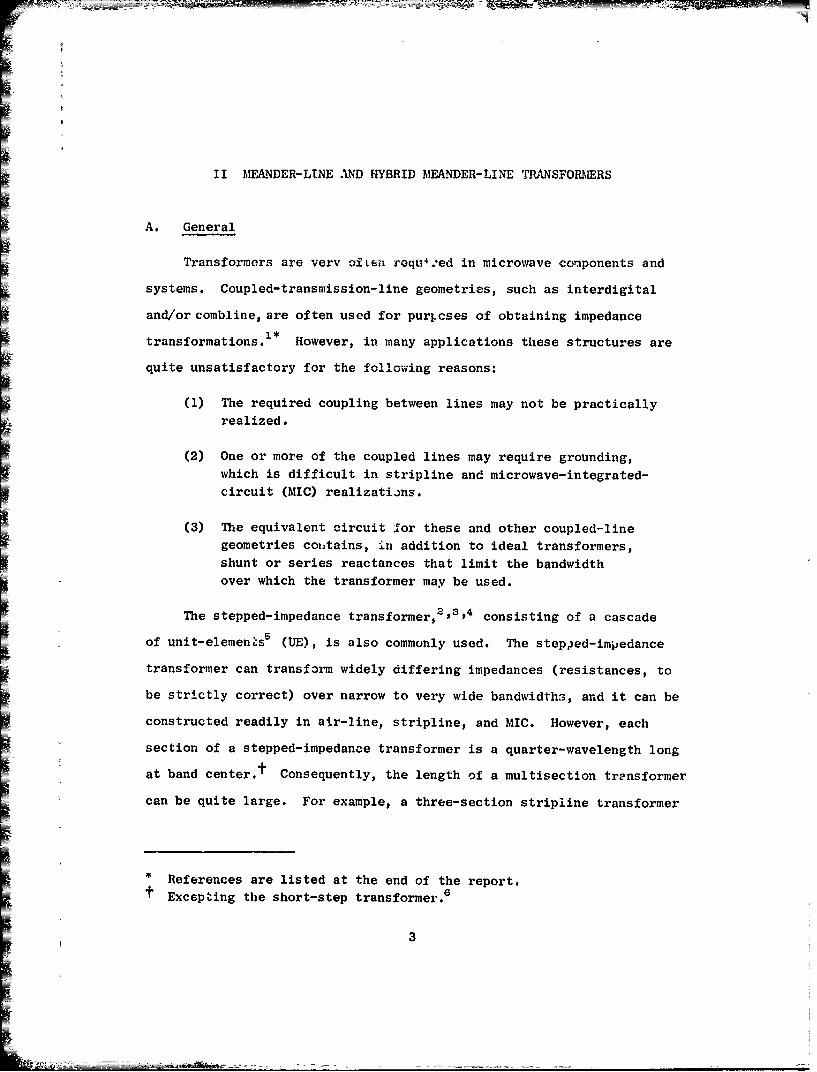
II MEANDER-LINE AND HYBRID MEANDER-LINE TRANSFORMERS
A. General
Transformers are verv ofiteI roqu 42ed in microwave components and
systems. Coupled-transmission-line geometries, such as interdigital
and/or combline, are often used for purj.cses of obtaining impedance
transformations. However, in many applications these structures are
quite unsatisfactory for the following reasons:
(1) The required coupling between lines may not be practically
realized.
(2) One or more of the coupled lines may require grounding,which is difficult in stripline and microwave-integrated-
circuit (MIC) realizatijns.
(3) The equivalent circuit for these and other coupled-linegeometries coihtains, In addition to ideal transformers,
shunt or series reactances that limit the bandwidth
over which the transformer may be used.
The stepped-impedance transformer,2 ,3,4 consisting of a cascade
of unit-elements5 (ME), is also commonly used. The stepped-impedance
transformer can transform widely differing impedances (resistances, to
be strictly correct) over narrow to very wide bandwidths, and it can be
constructed readily in air-line, stripline, and MIC. However, each
section of a stepped-impedance transformer is a quarter-wavelength long
at band center.t Consequently, the length of a multisection transformer
can be quite large. For example, a three-section stripline transformer
References are listed at the end of the report.Excepting the short-step transformer.6
3

constructed on Rexolite 1422 (e = 2.54) centered at 1000 MHz would ber
5.56 inches long. If, as is sometimes the case, transformers are
required at both the input and output of a device, che overall length
of the stepped-impedance transformers and device cozld be excessive.
An idealized solution to this problem would be to fold the stepped-
impedance transformer accordion fashion, as illustrated in Figures II-l(a)
and (b). In order to preserve the electrical characteristics of the
circuit, shielding between the folded lines would be needed. Conceptually,
this technique is satisfactory, but in practice the required shielding
would be impractical. On the other hand, if the shields were removed,
there would be sufficient coupling between lines to seriously degrade
the transformer performance.
Figures II-2(a) and (b) depict conventional meander-line geometries
in stripline and MIC. We note that these structures may be considered
as folded, coupled-line, stepped-impedance lines. Thus, from this
Z1 Z2 Z3 Z4
(a) UMFOLDED
V ,SHIELD
Z4Z
Z4
Rg R LA AL
(b) FOLOEDTA-8245-120
FIGURE I1-1 STEPPED-IMPEDANCE TRANSFORMER
4

Z '.
(a) STRIPLINE
...........................
(b) MICROWA.E-INTEGRATED CIRCUIT (MIC)
TA-2245-115
FIGURE 11-2 CONVFFIONAL MEANDER-LINE GEOMETRIES
perspective the meander line might be considered as comprising a class
of generalized coupled-line transformers within which the stepped-
impedance transformer is merely a special case for which coupling between
turns is negligible. From this point of view, an ext. asion of meander-
line transformers to hybrid meander-line transformers is quite natural.
A hybrid meander-line transformer is one in which coupling between some
adjacent turns is negligible, whereas for other adjacent turns it is
significant. Several examples of hybrid meander-line transforners are
given in Figures II-3(a), (b), and (c). Theoretically, the number of
hybrid configurations is 2 (N - 1, where N is the order of the transformer.
Hybrid geometries allow the circuit designer much greater flexibility
in the physical layout of the transformer than he would otherwise have
with only meander-line and stepped-impedance transformer-.
5

(a) EXAMPLE 1
(b) EXAMPLE
(W€ EXAMPLE 3
TA-8245-116
FIGURE 11-3 HYBRID MEANDER-LINE GEOMETRIES
The meander line is not a new transmission-line geometry. Butcher7
studied it from the point of view of its possible application in traveling-
wave tubes. Bolljahn and Matthaei8 computed its image impedance in the
general all-coupled-line case, and Hewitt9 utilized the structure in a
microwave compression filter. The most recent and novel treatment ofthe meander line has been given by Sato. 10 An equivalent circuit formeander lines (presented by Sato) having coupling only between adjacent turns
is given in Figure 11-4. The coupling between turns is accounted for
solely by "S-plane inductors"5111 connecting unit elements. A stepped-
impedavce geometry is obtained by setting all inductive admittance
values to zero. A hybrid geometry is obtained by setting some but not
all inductive admittance values to zero. The equivalent circuit of
6

ORIGINAL CIRCUIT EQUIVALENT CIRCUIT
Port 2, __ l')Port 2
N 0ODD
Port 1
EVENEVEN H-l Port I Port 2
Port 1 Port 2
TA-8245-121F FIGURE 11-4 TWO-PORT EQUIVALENT CIRCUITS FOR MEANDER LINES HAVINGNEGLIGIBLE COUPLING BETWEEN NONADJACENT TURNS
Figure 11-4 forms the basis for the compilation of meander-line trans-
former designs given later in this section.
B. Meander-Line-Transformer Design Tables
The meander-line transformer tables presented later in this section
were compiled using numeric. techniques by minimizing a weighted
reflection-coefficient function raised to a high integer power (e.g.,th
mi'iimizing a least-p objective). The weighting function was cun-
structed to assure that the coupling between meander-line turns would
be within prescribed limits. The numerical techniques are well known,12
and consequently specific details will not be given here.
7
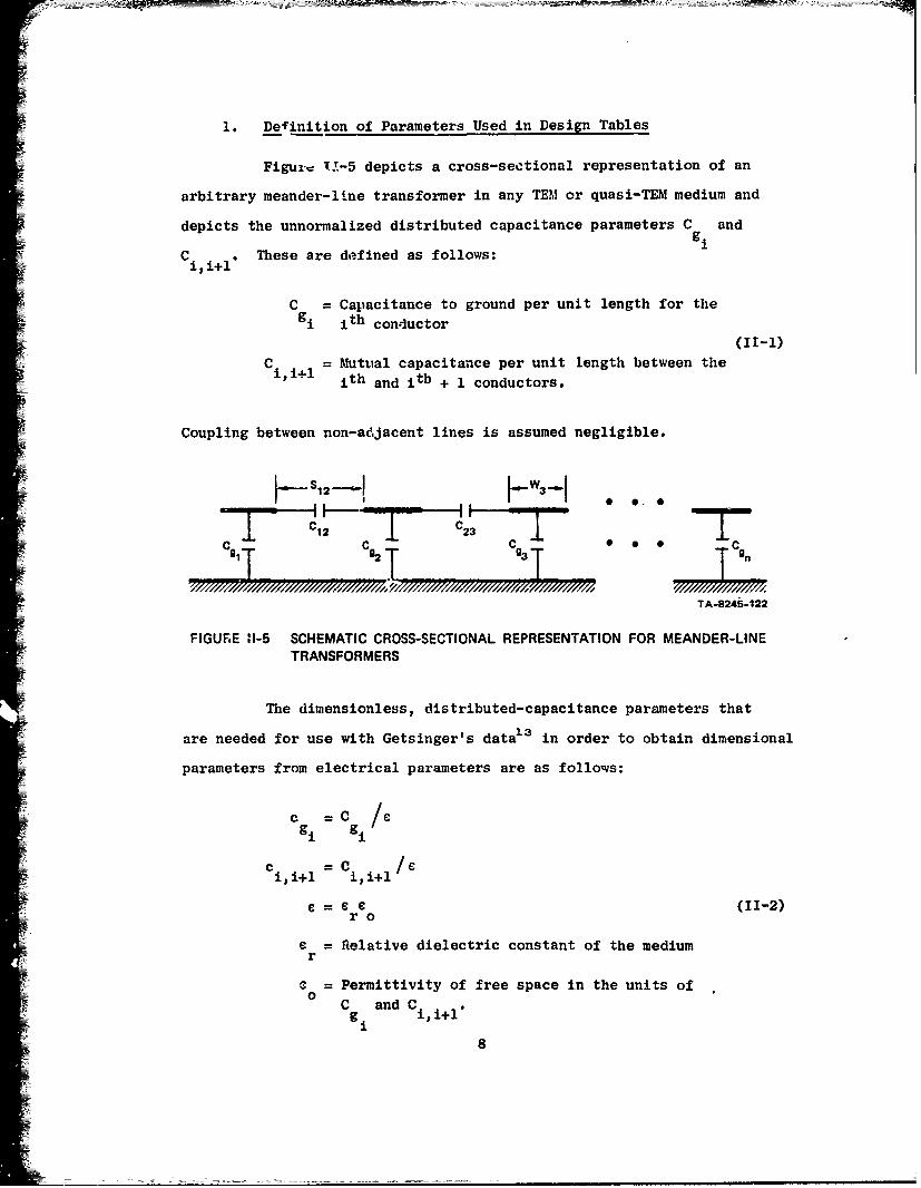
1. Definition of Parameters Used in Design Tables
Figura r-5 depicts a cross-sectional representation of an
arbitrary meander-itne transformer in any TEM or quasi-TEM medium and
depicts the unnormalized distributed capacitance parameters C and
C , These are defined as follows:
C = Capacitance to ground per unit length for thegi ith conductor
(II-1)
C = hutual capacitance per unit length between thei,i+l ith and itb + 1 conductors.
Coupling between non-adjacent lines is assumed negligible.
gc T 'T T Tc"TA-8245-122
FIGURE H1-5 SCHEMATIC CROSS-SECTIONAL REPRESENTATION FOR MEANDER-LINETRANSFORMERS
The dimensionless, distributed-capacitance parameters that
are needed for use with Getsinger's data 3 in order to obtain dimensional
parameters from electrical parameters are as follows:
C =C /£
c =C fei,i+l i,i+l
e = £€ (11-2)ro
C = Relative dielectric constant of the mediumr
C= Permittivity of free space in the units of0
C and Ct t+1
8

The coupling, k, 1 , between meander-line turns i and i+l is
Kdefined as
Ck =-20 log dBii1 (Cg + ii+l)
_ i gi+l
("1-3)
The meander-line-transformer bandwidth, BW, is defined as
BW (11-42/1 (I-4)
where e and 0 are the lower and upper passband edges, respectively, in1 2
electrical degrees or frequency. The ratio of load to source resistance,
always taken as greater than 1, is denoted by the symbol RL/RG, and the
peak VSWR in the passband is denoted by VSWR.
The compilation of meander-line-transformer designs is presented
in Table II-l, for N = 2 to 6 turns, RL/RG = 1.0 to 20.0, and BW = 1.5
to 10. The normalized self and mutual capacitances are listed under
the column headings CGi/E and CMij/E, respectively. These values may be con-
verted to the diwensionless forms C/e required by Getsinger's data, by the
equation
C
or _ 376.7 tTable II-i valuer (11-5)
ii+l r
where RG is the source resistance in ohms. Table II-1 was terminated
after the peak passband VSWR exceeded 1.5.
9

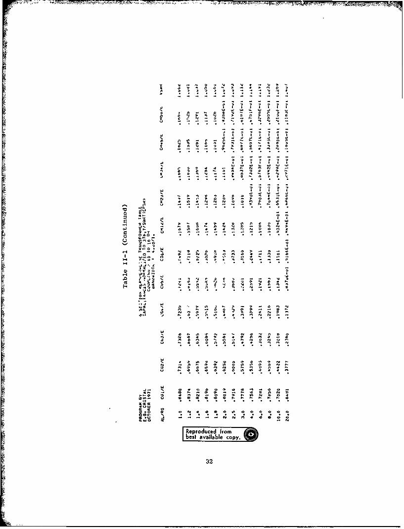
Table II-1
M~EANDER-LINE-TRANSFORMER DES IGNS
PROODM Hy2 CTIO OVANDER-ULNE TaANSFOPIEO TABLE
E.G.CRITALCADACTTANJ'Fq .N0R'AL!ZU Tn 3?6.71SOOTtEPSOI
MCORF.A 1971 T 6D
FL/AG Cfl1/v COW/ CM12/E V5.i
1.1 .011'4 .7?66 03754 .
1.2 .799. .7339 OW60 1.A11
1.3 .7Sq& .699. .1457 1.fn2p
1.4 .7743o *66P4 .134A I .0A
1.6 *7324 .5494 .145A 1.015
1.7 .MIA S5646 .14ni' 1.q1Q
i.0 .71-, .54p? *1347 1.144
1*9 Op- *s2ss .1241 1.447
6.6*772 .65 .1147 ."as
2.4 .6 65*7a 13 .A
2*1% .634% .39&? .q76Fftn 1.170
3.n A6347 .3912 qq'7pr.ql 1.q47
3.5 N6P47 .33R2 *n~qar-fj j.nqj%
4.4 51 .3146 T75U4P-ftl 1.11R
4.5 .5637 .2"11 *73?hvfl 1.1Pn
s.0 .5%i40 .26-1f' fS57r-fll I . IPi
&.0 *5.9;2 .22MA .615Q~Fll) 1.1%ft
7..1 *'e2oA .202;n s437F-01 1.IA7
8.a .4RPI j1d75 .495%Cvfl3 1.1R1
9.0t *47p? .17P1 *4599V-111 1.100
2C.0 .3941 *10 masQ-h 1.341
10

Table II-1 (Continued-)
'900PAu AY 2 SFCT!OnJ MEANDER4N TRANSFORlIEA TABLEE.S. CRISTAL C*PACTTANrVS NORMALIZEl TO 376.7.jSQ3TffPSR)
CC70PER 1971 efltPLIN0 * 0 To 16 08.1ANnw?OTN a2.00/1.
fiL/90 cGI/F 'GP/F C"VIVE v5wa
1.0 .7564 .7ss2 .2727 1.014i
.1 *2,k .?15S .2~56S 1.02?
1.2 .732, .66 .2359 1.'n41
1.3 M74'> W66 .215f , u'.
1.4 *76@6l 643 .134n j.fl7A
1.S .7504 .6064 .1242 1.04%
1.06 .744P *6u?9 .1235 l~nqA
1.7 .733Q S-JA4 .1194 1.111
1.4 .721A .5662 .1137 1.12?
1.9 .?)Z4 .540-1 1an 1.131
2.2 AA441 .4932 .9449E-nI 1.171
P.4 .4667 .4661 .927se-fti 1.144
2.1 .651Q .44 7 AAWl-01 1.2nt4
2.0 .06397 .4109 *6415F-DI1-21
3.n .424A .4,,n2 *R'qQE-ftI 1.244
3.5 *.1-0 *35Q# .1294v-niI1.A4
4.A .15771 .3275 *f72Ig -j !.125
4.S S561? 3.49 .41C79-01 1.3S4
5.' r,4cA *2A17 .58n3r-o1 1.391
S.. I?12 .249Q 51sj7F-nI1 1.4501
7.0 .49f)- .224A .47nIV-01 1.511
Rqproduced 1rom
best available copy
I Icopyt

Table 11-1 (Continued)
~IOSA~ qY2 SCTIONJ oFNEQ-LIN T49NSVOCsER TABLEE.G. CRISTALC*AIAq.CIhE.TO361SItSi
CCIO6E ml rfI;PLI%6 a 10 TO 16 09M*.1'WIOTh a 3.00/1.
*L/RS C01.'E COW/ CmI2,E vebwo
I.', -7A ~ 7374 *?1A n72 q
1.4 .7511- f. 71 *AIQ 1.4s7
.k .7?- .14;9 .123- I*S'll
PrCGRA" ay 2 SECTION vVAIJOER-LINE TRAMSFOR EP TABLEE.G. CRISTt. CAPACITANefg WCROALIZFn TO 3?641S3*(EPSR)CCTOAER 1971 PMlhPLING 6 10 TO 16 DO
AANbIOH *4.00/1.
fURG ml /V CGPIF C'412YE vSlie
lei -7A .60012 .2940 I.n~n
I.P *76A .72iA Ml6 1.121A
1.. *7814 .719;7 *13014 I ,lst
1.4 *7f6A2 *64~ .1297 1.723S
I*5 .749'. .64.t4 *22f 10031
.. 737c .6359 .1164, 1-33p
1.7 .?17-1 f. IP *11j. 1 .'*n
1.4 .. 30- .597Q .14:72 1.4217
hOQ .69rc .*71Q If,31 1.471
2.1 ?AQ0 *5S7Q .9940C-al1.1
aftknbfl1m a S.40/,1.
.142 *75' *5a .?2 1.nn
1.3 1784r *711A .13PQ ).?IQ
1.4 .7612 .6094 .131R 1.777
1.6 .7233 .64-9 1A 1.7
1.7 .7133 1410.1 .1128. 1.4&0
1.6 .7111 S5943 .11)51 1.s2Q
12

Table II-1 (Continued)
P~eqQM qy2 S~.T~flJ "~ ,,;ALIKE T0*A4SFOPEA TABLEE.6. CRISTAL CAPACTTVAlrFS NOR L!ZEn TO 376,7/SCf1TcEDSO)
CCTOnEP 171 1 IPL~bG 8 10 To 16 Da
RANtW1O1N a 6.00/1.I '/a f-ItE CGP/c CM12Z/E vswa
1.Z .781r, .7345k .17n2 1.161
C A P1 . . 4 3 1 fi q p 1 2 S ? 1 -3 1
1.6. 72 *6f .317 .1194 -n 1.4lr4
1.4 .61121 .41n .114A .5
2.6 *3~M A6AA A~qfrom
13
ReId~
ptc(;OAV~ ft tCm4#,S-L% p~~pr AL

Table II-1 (Continued)
P r~TO~ rhfA.--QLP~r TP~FlDRQ$8t' ?A2LfE c. C 1TAI CAParTAwI~ ,-CRV.L1Zrn T'4 376.?/SCRT~fPSQICCTC-MI-PP 1%6 a 11, A* to
0APtb1O!I - 10.00/#1.
I* *7 . 74AQ .?74- I.fnlI
1.1 . 7I.746 *4? 1.na4
1.4 .7C&7 Jk-,v~- .13&q .3A ca
E.G. CRISraL 3 SECIT OiAmr E MLIgEI)T 1 3A'.5VGQRICEPSR
dAkvwIOTm 2 1.50/1.
4LG GIE ,3/E CG/E C-41Z/E c~qzjIE VSuf
1. .86 ;'? .8 * 2604 .20% 1.Ouz
1.16 .2?d 1.00)
I ;. .64 SV? 715 .2604 .1"V6 1.uZS
1.5 .7038 *S2d3 .S66Z .2^93 ZG08 1S ?
1.6 .7425 .51"?2 532 .2o19 .1bsz 1.clb
I.' .72- .4l9 .99 .2-33 .13.5o 1.n13
1.9 .7211 .48d66 .0883 .1874 .11OU 1.012
2.m .7165 *479. *.~. .1990 .1151 .1
2.2 .716-1 .4697 .4414 .1604 .0976E-oi i.o1
2.4 .7?? .400j3 .42Z2 .1720 .62'0E-rii 1.019
2.0 .7414! .4646 .395S .1272 .8o7mE-c1 1.016
2.4 .141. .4SI-I .371-1 .128 -75W01o t.o~b
3.n .?292Z 4o .35o5 .1161 .621sZ-oi 1.017
3.5 .726v .4A62 .3o2a .1,116 6021E-ol 1.06
6.t .7039 .36.14 .2564 .913?E-al *.33JE-a1 1.o3S
4.5 .owaz .3S17 23N4 e$*41E-ol bM29E-;l 1.033S.1 .6098 .3314 .2237 .960SE-ol .53Z?E-o1 1.042
6.P .0575 .29 92 .14--2 .816SE-ol *49T1Z-ol 1.06
7.c .0502 .2671 .1b .7425E01 *47SIE-ol 1.053
8.A .6313 .2614 .14 79 .734CC-0i *3S,*E-01I1.o*V
9.0 .609b .2.9)l .1342 *73&?C-o1 .351-U-01 1.000
14.0 .6o23 .2304 .1214 .?ASIE-91 .JS3E-01 1.0*910.11 .5260 .1614 *0SJ -01j -534SE-01 .1927E-01 1.000
14

__ _ 7
Table II-1 (Continuad)
Pi~Oi4AAHY ECT I :C'i iA:'JER-L4iE IHANSFOOMIN rAULE5,E.G. CR4ISTA PAL1TI AlLS 04 J1Lt U 10 176. /SUHT( I~~OCTnA.ER 1971 COUPI-4d a la 10 16 Da.
RL/QG CC'I/L CU/t CoiE C-ie/E CMZ4" vbtWN
." *!J/ .*31 .d14 .273E1 .031E L .
I.?' .728b .5474 .0061 *6I7s 1 6 eE. 1 .0b7
1.3~ ~ ~~qroue .72 o, bU 2From lay I~j1.4 ~ ~ ~ bs availabl .51co Q .7py. I"
I .r, 687 b24 ~ f? .0)9 .56153

Table II-I (Continued)
PROARAM dY 3 SECTION mEANDOER-LI'4E TRANSFOqMCM TAULE
E.G CRISTAL CAPACITANCES ,'. MALIZED TO 376.7/SURTIEPSRIOCTOBER 1971 CUUPLI,G a 10 TO 16 04
dANk1D0Th 0 3.00/1.
ALNG COI/C C02/E CC-J/E CM12/E CM2J/E VSwH
1.1 *83 *6407 .73b0 .1334 ,Jobb 1028
1.1 .84b .6215 .6973 .1.03 .Zd? 1.02b
1.2 .203 b?877 .0916 .1406 .2b17 1.051
1.3 .8089 .5732 .6215 .1358 *2J61 1.01a
1.' BVS .b5s .b962 .1387 .2153 1.I.9b
1.5 .7799 .5*15 *b7(l .1352 .jYOV. 1.114
1,6 .7661 .5J26 *b484 .1250 .1783 1,29
)!7 7573 .b2b .5324 .123S *160" 1.1b
1.4 .7504 .520 .5171 .1176 .1*3* 1.1b7
1.Q .7406 .5144 .bOJS .110 .1277 1.1b7
2.n .721b .b16 *b.Jb .1221 01004 1.1Y3
2.2 .7230 .5161 .46!9 .1105 Hb17E-01 1.220
2.4 .7109 .4d2H .4387 .In20 *0543E-01 1.226
2.6 ,b91 .4711 .417S .9746E-01 .781*E-01 1.240
2.8 .6917 .4bb *j9b? .951CE-01 .7181E-01 1.2b8
3. .6766 .43b? .37M. .9228E-ol .lO2bE-01 1.28b
3.5 .6519 .4.15 .342 .85B8E-0) *bIIE-Cl 1.32o
4.l .63q2 .3757 .2941 *779bE-0l .399E-0l 1.391
4.5 .6142 .35,A .27bb .7626E-01 0]126E-01 1.414
S.^ .5979 .30i3 eb42 .7155E-01 .4?3uE-ul 1.457
6.0 .570b .312 2,17 .6891E01 .41IIE-o0 1.950
IReproduced from
best available copy.
16

Table II-1 (Cc::tinued)
E.G CHICL CAAC Tac. ~HM Lzc0uT3 6*7.sgI~OCTOMER 1971 C0UPL1.-G a 10. TO 16 04
dANU.'IDT1 a 4co0,1.
ISL/QG C'31/t C'2/E CG3/E CMI2/E CM23/E VSwR
1 .8102 A!1 78. .53 *Jbj 1.130
1.1 .8177 *628? .73J. .1747 .2307 1.068
1.2 .8)81 .61sh .696ti .1633 .1V75 1.103
1.3 .156 .*97A .6606 Is?7? .1U4* 1.124
1.4 .7?t)4 .bddi .6.1 .14b3 .1091 1.165
1.S .7691 .5d33 bibb6 .1388 .135, 1,197
I . *7537 5??3 .64,? .1321 .119b 1.2od
1.7 .74b6 Was5 Wib 1 .1231 .104V 1.232
1.' 7.1 Sei? *6es .1161 *997VE-111 1.2b2
;.9 .72bi .6416 .539b .1132 *9557E-Ul 1.2V7
2.,1 021b .bjs, b2b2 .1'.7d V914bE-l 1.3u0
2.? 07061 .*11.4 .*bv7 .1419 *5605E-01 1.3bg
P.4 .6556 .491S .4"t5 *9'10-01 .'SU0eE-01 1.4U3
2.6 .6735 .47bi .4369 *9S18E.-Pl *749bE-01 1.4%b
204 *6b46 .464? f~jIq *9)bTE.O1 *706*E-01 1.02,
3.,, .65j4 .44bb .Jyb9 *653SE-01 .,b7E-vI 1.529
PR04AM B 1 CJ. ASO,5QfE.G. CISTAL 'AC t T 7. R~JCTnHLA 3971 COUPLINJG a 10 TO 16 00dANuwUICTm a 5.00/1.
.IL/PG CUM/e COV/E CtOA/E C.412/E C#M23/E VSSII
I..' .963b .(6376 .737H4 .151b .4167 1.002
1.1 .8326 .613, .7198 .1799 .2bio 1.06U
I .P .796? .597#i .bH48 .1681 .2281 1.115
1.3 .7013 .586-1 .0667 .1524 .2017 1.164
1.4 .7588 b6?, .b426 .1569 .1071 1.211
.. 7620 bvb6i .6403 .1326 .122b 1.246
1.6 .7527 .589b .6159 .0233 .1114' 1-260
1.7 0?390 .69P .:191,6 .1202 .1091 1.3d6
3.8 .130o .5601 .5719 .113? .1016 1.361
1.q .71I54 .51#t4 .55,14 .1100 .9596E-0l 1,399
2.n .7075 .b34l .5344 .1P72 .9346E.01 1.433
2.2 .699b .5121 .4999 .11002 dbdtjE-oi 1.5u7
best avaiabe copy_F
17

Table II-1 (Continued)
PHOGRAM BY 3 SECTION MEANUER-LIdE TRANSFORMER TAVLEE.0G C4|STAL CAPACI A ECS NORMA LIZEO TO 76.?/SQRT(EPSR)OCTOJBER 1971 COUPLING a 10 TO 16 DS
OANUWLDTH 8 6.00/1.
RLIG CGI/E COVE CG3/L CM12/E CM23/E VSIR
1.1) .61#05 *699 .77!j6 .1023 .260 16015
1.1 S0222 .6314 .7319 .1661 .2381 1.06b
1. .8r46 .6134 .6937 .1S41 .212u 1.1J4
1.3 .7Y27 641 .6669 .1415 *10TU 1.194
1.4 977J3 .610 .6616 .1409 .137b 1.246
1.5 .7617 .6057 .6493 0)286 .1207 1.292
1.h .7501 S)O0 .6196 .1242 .1136 1.351
1.7 7357 .57515 .5993 .1185 .1071 1.39b
I.3 .7194 .5561 .577 .11S7 .103V 1.446
1.9 .7100 .b09 .5576 .1099 .9USbE-01 1.492
2.A .6910 .2328 .53V9 .1079 .9487E-01 1.SJ9
P40RAM eY 3 SECTION MLAN0EA-LIdE TRANSFORMER TAULEE.G. CWISTAL CAPACITANCES NORMALIZEU 10 376.T/SGNT(EPSR)OCTtdER 1971 COUPLING a 10 TO 16 0
UANUWIUTH 2 8.0,/1.
RL/-1G CGVE CO2E CG3/E CM12/E CM23/E VSWM
I.n .7992 .61#1 .7926 .2315 .24"1 1.025
1.1 .7ou .6171 7484 .2117 .1996 1.00b
1.2 .76tsI .607 .7217 .2np*9 .1761 1.16o
1.3 .7012 .6222 .693 .14S7 .1jb7 1.231
1.4 .771 .6197 .6673 .1393 .137 1.301
I,1 .780o .6019 ,b4b2 .131t .1239 1.3t7
I.6 .7#32 ,bd4 .622s0 .1237 .1143 10 4
1.? .7311 .574o .604 .1168 .102 1.498
1.9 .7133 .5689 .5834 .1164 .1028 l.Sb2
CRA !8& ;E f A FO I" TAN OR§§ ITJJ
OCTmdER 1971 CUUPLIiG a 1o TO 16 0
dANUWIOTH t 10.00/1.
RL.'04 C6)/E CO2E CG3/E C'12/E CMZJ/E VSam
1.11 .9361 .67h9 .8014 .1022 .22&U 10004
1.1 .6174 .S,1 4 ,SV2 .1733 .2009 1.086
1P 06n17 .63d3 .7266 .1615 .170d 1.0171
1.3 .708? .6314 .7?os .14-8 .1449 1.253
1.4 .7769 624, .008 .136o .12*4 1.331
1.S .7563 .6011 .6484 .1329 .1221 1.409
1.6 .7364 .590S .6208 .1265 .114, 1.416
1.7 .7260 .5694 .6010 .1202 .1119 1.560
18

Tale II-1 (Continued)
PROGRAN BY 4 SECTION MEAhUEM-Ll4E TRANSFOQMER TAOLEE.$. CRISTAL CAPACITANCES NORMALIZEO T0 37,.7/Sg,47EPSH)OCTOeER 1971 COUPLING 1 10 TO 16 118
dAhudl)rH 2 1.50/1.
RL/AG CGVE COV/E CO3VE CG/E CM1/E C0423/E CM341E VSwl
I.0 .6161 ,7046 .7046 48161 .216 .1598 ,2167 1.216
1.1 .6199 .6658 .6919 .7889 *197U .1583 .1469 1.001
1.2 08046 .741 .6640 .727 .197U .131b .1300 1,oul
1.3 .8327 .6462 .6059 *6R51 .1b6J .176b .1197 1.Ui
1.4 .8236 .6420 .57bz .6237 .1b .1449 .129?7 1.003
1PS *8241 .6278 .549? .5847 ,#d% .1439 .177 1.00e
1.6 08150 06117 .599 5ss56 .1b17 .139b .108 1.oo
1.7 .8116 0042 .503 .5240 .149e Ltu .1091 1-0o
1.3 08029 .5915 .4678 .4938 *1b21 .1205 ,1001 10o
1.9 07945 *5769 .4727 .4728 1*j3V .1171 .9923E-01 1.002
2.0 .7954 .5695 .4617 .4560 .1533 .1228 *92d7E-01 I.OOJ
2.2 .7916 .5593 1 .4099 .154 .1055 .9533E-01 1.003
2.4 .7796 .5403 .4,64 .3654 L1~bb l1oll .403E-01 1.oo4
2,6 *766- .52S .3918 .34h .1521 ,4323E-01 .*37bbE-01 1.0ob
2.8 .?673 .4v61 .3622 .3338 .139 .1083 .7231E-01 1.tob
3.0 7626 .4901 .349b .319 .14#1 ,*122E-cI .706RE-01 1.0)'
3.5 .7521 .4741 .315H4 .26b4 .IS?.* .oudUE.o1 *.60E-Oi I.OuD
4.0 .7509 .4637 .2966 .24U5 .134b .7616E-01 .5735F-01 1.006
4,5 .7316 .436-) .2715 .7153 .13bv 6989E-01 .iuOE-01 1.000
5.0 .TJ02 .4236 .2525 .1750 .1300 .6b23E-o1 .483E-01 1,007
6.0 7209 .4046 .2300 .1677 1e9b .b3SIE-01 .4111E-01 1.005
7.0 .7146 .3840 .2062 .1453 .111 .2690E-01 *3534E-01 1.UO
8.0 .6982 .303! .1881 .1262 .1214 b5350E-01 3292E-01 1.010
9.0 .6944 ,3491 .1741 .1156 *11je ,317JE-n! ,29U5E-01 1.01u
10.0 .6760 .3311" gb0 . ls? .11do *4984E-1 2608E-01 1.011
20.0 .6929 .302C .114 ,SQObE-01 V9U02E-01 .,79SE-01 .1606E-01 1.oe
19

Table II-i (Continued)
FACGRAM A V SECTION MFANDER-LINE TRANSFORPER TABLEto$. CAISTAL CAPACTYANCFS NCROALIZED TO 376.7iSQPT1EP$RICCTflHER 10?1 cfUPLING 4 10 To 16 08
PANDWI1Th 8 2.00/1.
.L/RG CGI/E CG2/E CO3VE CG41i CMIV2E CM231 C"34/E VShR
1.0 .0365 .1172 .7233 .8436 .1414 .1559 .17 1 1.000
1*1 .8379 .6455 .6725 0?732 .1s58 Is?5 .16p6 1.003
1.2 .823? .6677 .6357 716s .1713 .1527 1.110 1.005
1.3 *0208 .6539 .6059 .6685 ,112? .1448 .1399 1.000
1.4 *857 .6.00 0582L .629n ISO7 .1372 .1276 1.009
1.5 *8129 .6315 5635 .5962 143p .1273 .1179 ;.1
1.6 ,56 .616S .5J95 .5593 .1530 .1224 .1143 1.014
1.7 .797? .6324 .5146 .524A IS531 .1167 .11S2 1.016
1.4 .702n sno .4451 ,So13 .1454 .1188 .1069 1.017
1.9 .7917 .5816 .41439 .4801 .1463 .1113 .99?qE-01 1.019
2.c .1894 *L 1 3 4 ,*6R2 .458? .142 ,1072 ,SqOE-*O 1.020
i.2 *717 .5499 .4363 .4214 .,18n .1070 #8967f-01 1.023
2.4 .7?35 .5339 .4123 .3883 *13Sn .1009 .8404E-01 1*026
i.6 .7671 .5208 .938 .3626 .13?5 *9512E-01 *7754E-01 1.02a
.8 .76s5 .5115 .3755 .3395 .1159 ,115E-01 ,73P1E-01 1.030
3.0 .75 .. Vtc, .'481 .319g .1273 *8977E-01 .6975E-01 1.033
3.5 741 .46I .323b .2778 .1212 .8265E-01 *62n90E-01 1.036
4.p .7331 4.4m2 .298S .2470 .1178 .7540E-01 .SS42E-01 1.042
6.5 .7 ?7 .4333 *2778 .2231 .1113 .7015E-01 .4994E-01 1.045
Sou 0716c .41S3 .2592 .2031 .1102 .6644E-01 .4623E-01 1.050
6.0 .7n44 .392o .2317 .1731 .135 .5934E-01 .39SoE-01 1.055
.,) .691P .3705 .2106 .1514 .100 .5464E-01 .3442E-01 1.062
8.0 .6799 .3532 .1934 .1347 .9687E-01 .sor9E-O .3099E-01 1.067
9.0 .0717 .3384 .1767 .1212 .0219E-01 .4613E-01 .2032E-01 1.072
10.0 .06b9A .329S .1695 .111n ,79sE-01 .4514E-01 .25670-01 1.074
2(,..) *117 .2545 .1085 .6054E-01 *7259E-1 .3099E-01 .1468E-01 1.111
20

Table II-1 (Continued)
PROGRAM BY 4 SECTION HEANOLJ-LIIE TRANSFORMER TAULEE.G. CRISTAL CAPACITANCES IdORMALIZED TO 37A.7/SQWT(EPSR)OCTOBER 1971 COUPLING a 10 10 16 OR
dANUdIDTH 8 3.00/1.
RLIRO CGI/E CO2E C03/E CG4/E CHI/E CM23/E CH3W/E VSw.
1.o .6551 .7455 .7433 .852b .16l9 .13bb .1621 1.0Ou
1.1 .8269 .bd17 .6691 .7761 .1766 .1659 .1638 1.014
1.2 '8122 .6666 .6516 .72b7 .jTT, .1440 .1430 1.027
1.3 .8151 .65b9 .6209 .6789 'pug9 .1344 *1360 1.u39
1.4 .8114 .6421 .926 .6391 .1503 .1329 .1264 I.Ob0
1.5 .8062 .6294 S696 .6026 .1443 .1257 .1194 1.060
1.6 .7979 .6147 .5483 .9704 .142J .1202 .1139 1.06"
1.7 .7941 .60,3 .5297 .5426 .146J ..1151 .1079 1.076
1.8 .7864 .S918 .6128 *5178 .1351 .1116 .1021 1.089
1.9 .?8J2 .5821 .4973 .498 .130J .107u .9729E-01 1#08Y
2.0 .7757 .5699 .4826 .4744 .1298 .1041 .929SE-01 1.09
2.2 .7662 .S516 .4562 .4302 .1Z47 *0620E-01 *6567E-01 1.107
2.4 .7566 .5351 .4334 .4076 .1213 .9283E-01 .7974E-01 1.118
2.6 .7484 .5203 .4134 .3814 .1176 .6843E-01 .7439E-01 1.129
2.8 .7406 .508 .3955 *358? .1140 .8477E-01 .6980E-01 1.139
3.0 .?337 .4946 .3794 .3386 .11U9 .5138E-01 .658OE01 1.14b
3.5 .7171 .4670 .3469 .29.7 .107 .e4SOE-01 #5730E-01 1.168
4.0 .?o22 .4465 .3208 .2672 .102d .b616E-01 .5172E-01 1.189
4.5 .6900 .4274 .29.5 .2421 .9739E-01 *6390E-01 .4710E-01 1.206
5.0 .6794 .4112 .2000 .2219 .9319C-01 ,b03?E-01 .4323E-01 1.223
6.0 .6600 .3841 .2S14 .1913 .8767E-01 .54SIE-01 .3697E-01 1#256
7.0 .6452 .3633 .2293 .1606 .227E-01 .5040OF01 .32SAE-01 s.28J
8.0 .6300 .3451 .?114 .1510 .777E-01 .0667E-01 .2944E-01 1.310
9.0 .6103 .3305 .1973 .1373 .1525E-01 .4372E-O1 -2678E-01 1.334
10.0 *607? .3174 *1857 .1262 .7278E-01 .4122E-01 .2463E-01 1.358
20.0 .S429 .250? .1263 .7344E-01 .5b83E-01 .2738E-o1 .1443E-01 1.550
21

Table II-1 (Continued)
PROGRAM By 4 SEC tO MEANDER-LIE TRANSFORMER TAULEE.G. CRZSTAL CAPACI.ANCS NORMALIZED TO 376.7/SORTIEPSR)OCTOBER 1971 CUUPLING a to TO 16 08
dANOIOTA 2 4.90/1.
ML/RG CGX/E CG2E CG3/E C041E CHI/E CM23/E CM34/E VSWd
1.0 *8179 .?126 7265 .8339 .9054 .1393 .1851 1.000
1.1 .U052 .6000 .67o 0Te0 .198b .1*35 .1623 1.02d
1.2 .8586 .6730 .6514 7313 1614 .1446b .1467 I.uS2
1.3 .8143 .668 .6217 .6816 .1481 *1325 .14aS 1.071
1.4 .8045 .6433 Wb1*4 .6486 .14JU .1283 .1261 1.09
1.5 7993 .6324 .bTT1 .609 .135d .1191 .1234 1411b
1.6 .7186 .6139 .5590 .5835 .13b1 .1174 .1115 1#131
1.7 .7031 .6034 .5426 .5569 .1JOI .1111 .1043 1.15d
1.8 .77s .5899 .!2b3 5320 .128e *1075 *990oE-01 1.1?
1.9 .7676 .578b b6094 .5097 .1040 .1039 .4524E-01 1.11b
2, .1607 ,5681 .4939 .496 IV9 .100b .911SE-01 1.199
2.2 0T482 ,$89 .469Hl .4S54 011fi *4SoUE-01 .8312E-01 1#224
46 .693 .5303 .31 9 .271 .112b iOu1E-01 .07739E-01 1.2tv
2.6 .72' oblsg $4274 .3Y96 .1jUv .9sgBE-ofl .72*gEoo1 102M
2.8 0715b .5021 .4U96 .37b9 .1056 .8Z04E001 .6056E-01 1#294
.' 4893 .3941 .3573 .10V7 .7867C-01 .44?1E001 1031b
J.2 .672 .464% .3633 .318v .969vE-Ot .?065E-01 b 64VE-01 1*363
4,0 .6691 .*4n7 ,33b9 .2871 .100TOE-O| 0626bE-01 .57dE-O1 1*410
4.5 .6522 .4197 .3133 .2612 .02JE-01 .62OOE-01 .4679E-01 1.4Sb
S.O .6384 *4e28 .29b) .2.09 .044kE-01 . iSYE-o1 .4294E-01 1.49
6.4 .6176 .37Y4 .2609 .214ps .1VE-o1 .529E-l1 .3727E-01 1.57e
22

Table I1-1 (Continued)
PRO RtH 81 4 SECTIO 101 ANOE:;LIdETA*NSFOQME TAULEE.G. CRITA. CAPACITANCES NIONALIZED TO 116.?/S;IkT(EPSR)OCT08FR4 971 CUJPLINGO a 10 TO 16 0.4
dAllt)810r14 a 5.00/1.
RLUNG COliC CGZ/E CG3/E C134/E Cf~l1d/E CN423/E C434/E V5.44
1.ft AM2 .71,28 .?19% .8481 .1920 .1675 .1679 1.ocu
1.1 0833? *8879 b68is .7Q07 .1fa41 .1662 .1491 1.046
1.2 .8232 .68f)5 .65711 .7361 .163's .1406 .12 1.083
1.3 .M04 .6b12 .6296 .6896 .11#9d .1298 .1376 1.11b
1.4 *8026 .0466 .6086 .6S6? .1381 .1250 .1240 1.144
1.5 07893 .6283 .5vb3 .6213 .1350p .1191 .1193 1.1?3
14A .7802 .6130 .5671 .5962 .1306 91150 .1100 1.200
1.7 .7709 .0001 .b~u5 .5671 .120 .1095 .1041 1422t,
1.8 .023 .5b72 .5333 .5442 .1220 .1060 *9901E-01 1.251
1.9 97S35 .5759 .5177 S5219 o.1204 O1016 .9513E-01 1.277
2.0 .?4S8 .5646 *5o2v .5021 .117d .98119E-01 .409VE-C1 1-30J
2.20 .?3o? .6446 .4776 .4679 .1126 #9323E-ol .8403E-01 1.347
2.4 *7175 *5269 .4559 .4393 .1081 d867E-01 .7?183E-0l 1.388
2.6 47046 .S10g .4366 .4143 .1043 .d44SE-ol .12V-E-01 1.42?
2.8 .692b .49b3 .4191 .3S23 .101f G80ODE-fi t..399E.J1 1.464
3.0 .6913 .4d30 .4032 .3726 *9?91E-o1 .7S4E-.o1 .54VE-o ,.!:ou
PAG3RAM RY 4 5ECT 10. HtAI40EI4.L 4 E THANSV02E4 TAU IEE.B. CRISTAL CAPACI TAN LS NORI4ALI1 EO TO 3?b..7/SoRt PS-1)OCTOBER 197! COUPLING x 10 TO 16 04
dANUOIT4 a 6.00/1.
AL/AG COM/ C412/E C413/L CG4/E L0eileE 6CM230E CMF./E VS...
1.0 .85o7 .7382 .7338 .8536 L64's .1535 .1611 1.000u
1.1 .8239 .69q2 .6097 .7911 .1130i .15,!4 .1502 1.obb
1.2 .8214 .6799 .6552 .7340 .1643 .1403 .14b7 1.101
1.3 .8019 .6584 .6297 .69b0 .1466 .1348 .134-0 1.1so
1.4 .7951 .0416 b6191 .6S91 .14 t# .1262 .12f#4 1.191
1.5 .784b .6266 .5692 .6281 .1.'v .1193 .1170 1.pae,
1.6 .7734 .6115 b?,13 .5990! jd .1139 .1113 1.26
1.7 .7631 .5975 .5538 .5746 .121d .1096 .1040 1.3ou
1.5 .752m .5847 5331 .5513 .191.1 .105r, .99O0E-01 1.336
1.9 .7627 .5726 .5223 .530ts lieu .1010 *95bbE-01 1.21.5
2.0 .7334 .5611 .b083 .5121 .1152 .4874E-nl .914toE-01 1.399
2.2 .7168 .S403 .4836 .4791 .1100 .0297C-01 R40u6E-01 1.4el
2.4 .7011 .%215 AM62 .4502 .1061 .0953E-01 .7871E-01 1.521
23

Table II-1 (Continued)
PRA*M ST * SECTION HtAf 0ER.LO'E TRANSFORMER~ TAULEMo COSTAL CAPACITAN.CES NOAHALIZCo To 376.?/SQRTtE9S";OCTOBE9t 1971 COUPLING a lo TO 16 00
JAt4UNIOTN 8 0.00/1.
AL/eO COVE~ COVE COVEC CG4i' CM12/E C23E CM3*/E vSw"
Ion .8545 *7397 .7481 .8662 .1bvO .1462 .3481 1.001)
1.1 .0215 .6916 .6875 .7862 .1140 .146* IS76 1.071
1.2 .S140 .6786 .0563 .7371 .1b3? .1408 .1069 1.13?
1.3 .8052 *b"89 .6318 .6968 .*63 .1329 .033b 1.201
1.4 .7902 .6411 .6106 *6621 .1414 *1239 .1259 1.2S7
1.5 *?o o6238 S5903 .6319 .1360 .d18l .1190 1.312
1.6 .7644 .6064 .572b .6091 .11914 .1136 .112Y 1936t,
1.7 *752O .S932 .S5b6 .5819 .1240 .1097 .1064 1.41lb
Ion .7396 *5797 .5408 .56o1 .1211 .10S9 .101? 1.46
1.9 .7294 .5675 .526S *s4os .117? *1022 .9?%9E-01 1.5ito
PROGRAM By 4 SEC710ft *A'4OERLI'.E TRANSFORMER TAbLEE.0. CRISTAL CAPACITAMCtS 4O.4MALIZED TO 374.7/SQ'HT(EPSR)OCTOBER 1971 CUIJPLING a 10 To 16 flq
dANU6(IDTH a 10.ifl/1.
RL/40 COI CG2/E COVEC CG*I/E CM1Ufe C%2J/E CN4IE vs.4-
Ion .R634 .1546 .7631 .8729 .11444 .1361 .131? 1.00.)
101 .8318 .6932 .617? .?812 .1054 .1573 .161(1 1.0hz
1.2 .d1st #6752 .6b56 .7381 .1b6U .142S .1401 1.15t)
1.3 .8041 .6592 *6p.IJ .692? .106,3 .1321 .1411 1.2?PV
1.4 .7896 .6002 .6.SSe .6623 .1*12 .1261 .1211 1.3ou
1.5 .77.37 .6216 03901 .6339 .1356 .1203 .1141 1.36,)
1.6 .7594 .6062 .5722 .607? .1jej .110' .1148 1.4.31
1.7 .7.62 .5901 .S5bs Stjo,- U160 .1106 116 .4,12
1.1 .0331 .5I5S 0410 S6837 U122 .1075 .10.35 1,558
24

Table II-1 (Continued)
Pacenm "y S SECTION MEANDER-LINE TRANSFORMER AB~LEto#* CRISTIL CAPACITANCES NONALT21O TO 376.7jSQRYTEPSRIOCTOBER 1971 COUPLING 8 10 Tri 16 o
MN' OIN 0 2.01.
ALAIS C911E COVE1 COV.E 004/f COVE1 CMll/c C"WEi CM36/E CP&4S/f vswp
1.0 .831" .6353 .6719 .6641 .4147 01867 .196i .2666 .2091 1.001
2.0 .8ft~fl .667 .4741 .4097 .4739 .1530 01992 Ii'43 .121? 1.006
R.2 *0031 .5553 .4629 .45-6 .408? .1512 WjO .9661-01 .8.S1e01 1009
2.4 .7898 .5665 .4625 .3700 .1704 .1604 413? .92261.01 .652Ei.01 1.010
2.6 .7695 *57fl0 .4514 *344 .34S6 .1649 .1144 .8974E-01 71 101010
2.6 m7S6 .5451 .4394 .3324 .3241 v1523 0109? J15099-01 .710ME-01 1.812
3.o .789a .6529 .4212 .3156 .3646 .1444 . 6224ESn.-01 .6623E-01 1.011
3.S .?602 .56 .3982 .2604 .2634 .1402 41022 .7310;-01 .13812E-01 1.01240 76 Sal .63 *2569 .2141 .133S .7410 .6ssse-o1 .496S1-01 1.013
4s .7666 :47324 .304 .1617 *1696 .1256 .90621-01 S5953E-01 .3S67-01 1.020
T*W' *76 4# 229 .61 1389 .1296 .72771.01 .4679E-01 .316"E-01 1.020
Er6oo0 .32 .4376 .2624 .153f .1227 .1260 .73621.01 .412SE-01 .27699.61 1.023
9.0) .729? .4272 .2466 .1319 .1;98 .1233 #6952E-01 .38s1-01 PS697E-01 1.024
18.0 .7273 .4173 .2328 .1,163 .169 *1111 .63021.01 .3803E-01 .224E01 1.026
16.0 .'%943 .391)8 .166m .77361-01 .';264E-01 .99661.01 .49i2f-01 .22971.-01 *i26RE6112.040
25

Table 11-1 (Contihiedu )
BSoUt RA lIS24O1 j~A~F*E ALE
oCTomIm 1071 COlUPL~IN16 TO 16 0o7S fKPR*Ih!O? a3.00A1.
ftLuUC C4119 C62/K C43/9 C04/f coS/E C"l2/E Clopvt CM34/l C045/t VSWR
1.0 *?&Go e6433 .1039 .644 .7669 J2799 .1796 *1794 .279A 1.00
1.1 .7467 .4396 .6890 .6273 *7p64 .2973 .j4" *1s3 .2z37 l.o00A
1.2 .7617 .4319 .6727 .6010 .4792 .2919 ilsxi *1333 .2034 1.015
1.3 .7769 .6391 .4461 .9670 *E176 .2301 .1444 .1398 Mn92 1.421
1.4 .7717 .4244 9623i .5642 .629, .219o .1366 41299 .130p 1.027
1.s 04686 .*47 *15931 .937t .9p59 .1633 .1307 .1261 .1237 2.031
1.4 .afte .4332 .9022 .4208 .5576 *1S&9 .1296 .1172 .1114 l.fj34
so? .464 .6310 .953 .4973 spflo .1908 012%2 01131 .10oit 1.M3
1.9 .0039 422 Osseo .4773 Sall1 .1479 .1220 .1o65 Iola 1.q43
19% 0093 6143 .931 O4996i .4776 .1064 .1193 .1648 .9393E-01l 148
see 07907 .404 *siz9 .4433 .4544 .1435 .1161 IiI 3 .9113E-01 1.050
got .7094 618?1 .4923 .4108 .4182 e.392 .1196 .184r-01 .8597K-01 10057
8.4 .7649 .5602 .4900 .3R8n .3099 .136o .1048 .6863K-Cl .803EK-01 1.062
. ??a7t $083W .&S94 .366a .3568 .1324 .1040 .8367K-Cl .7374E-01 1.067
Its .774? '5934 * '499 .3402 0377 *12'05 .9693K-Cl .601&K-cl .669e1Kl : 71
See .7400 .5447 .4288 .3335 .3182 #127w .9862K-01 .767E-02 .64OSKCI1 ..076
2.9 *754? .5221 .3994 .2994 .277; .1245 *9062E-0l #641E7-01 Sb9691C 1.087
4.6 .7474 .5044 .3746 .2731 .P441 Ollie .O62if-0l .6213E-01 .6020K-Cl 1.096
4.9 .7397 .49i1 .2541 mis1 .2,218 .1140 .96ic6-0l .9746K-Cl *450A6K01 1.105
SO$ .7341 .4774 .3364 .2342 P2AZS .1108 .17j6-01 .9319K-Cl 4074K1O 1.111
6 .7149 04918 .3163 .2854 .172o .1045 .7146K-Cl .4767K-Cl .3502K-0l 1.128
7.s .7049 .4323 .2840 .1841, .1969 .1030 *6466-01 .4350K-cl .303RK-Cl 1.140
set .4942 .4163 .2ust .l68 .1338 .9944K.81 .427K-OX .3915K-Cl .7710K-Cl 1.193
9.6 .005 .6~0 .2515 .1949 .1204 .1931-01 .591-Cl .3654K-ol .2474KC1l 1.165
10.6 .4714 .3911 .2386 .1444 .1102 .913S9-Cl .57j5K-01 .3424K-Cl .223GK-0l 1.175
s0.t .4211 .3174 .1493 .696KE-Cl .6037K-Cl .7728-Cl .4139K-Cl .2123K-Cl .124PK-Cl 14256
26

Table II-i (Continued)
PAMOemw 5t S SECTION MEANDER-LIkE TRANSFORMER TARLEf.0. CRISTAL CAPACITANCES NOROALIZEO TO 376.71S9AT(EPSO)
OCyOeIr 1971 COUPLING 4 10 to 16 09AINDUIDTH a 4.00/1.
*Le# C61/1 COVE C33nE C::/r eS/E C:12E C:23/E C.434i1 cw:s/c VS:
14l AM~ 97288 .7312 .7333 .4543 .1588 0i633 .1Sz .1603 1.000
1.1 .8366 .9674 .6816 *6648 .7751 .166' .16,3 .:654 .1619 1.017
1.2 s8293 .6163 .6601 .6365 .772; .1594 .1447 *1sog .1482 1.031
1.3 .0214 ,6726 .6419 l0se .6769 ,1S94 .1416 .1370 .135? 1.044
1.4 8160 .6614 .6216 *S772 .A161 .1496 .1346 .1285 .126f) 1.0S6
1.1 ,8099 ,6496 .6024 .SSo7 887 .1456 .1294 .1217 .1195 1.0A
1.0 s@037 .6399 ,SiS .5275 .S661 .1430 .1231 .1156 .1130 1.n79
is? *7983 .sls .5701 .So07 .slS .1399 .110Q .1103 .1074 1.090
1.8 .7931 06202 .5554 .4884 *SIZS .1373 .1159 .1;S6 .101 1.100
1.9 ,7894 .6120 ,S436 04742 ,4407 .134S ,11P7 .995SE-Ol .9406E-01 1.1ll
Igo .7833 .0010 052?3 .461 .4493 .1329 0111i Q@27E-01 .9142E-01 1.114
S. .7793 .g8m6 .5038 .4291 .4338 *1283 .1071 .9213E-01 .427PE-01 1.137
3.4 *76t7 .5.14 .4841 .4nS1 .4626 .1254 .1022 *8608Eo01 .7664E-01 1.1S3
20 .7599 .5393 .4066 .3846 .376S .1220 .9783E-D1 .8140E-01 .7124E-01 1.16S
2.8 .7S9S .5467 .4902 .36S9 .3S34 .1196 .94&PE-01 .?7110-l .6699E-01 1.178
3*0 .7444 .S35? .4356 .39ro .33@ .117? 091S1E-01 .7406[-01 .6?7AK01 1.189
3.S .729? .513 04034 .3170 .P93S .1123 .85ibE-01 .6636E-01 .50KE-onl 1.21A
460 .7177 .4930 .3795 A1893 .7618 .1064 .7946K-tl .6004E-01 .489SE-al 1.242
4.1 .7n04 .47?S .3S13 *2687 .2376 .1440 o#S89E-01 .597E-01 .439S-01 1.26
9.0 .6947 .4600 .3406 ISO* '2176 .999TE-l .724E-01 .5260E-01 .3999K-01 1.2A4
0.0 .67. ,43S8 .3122 .2213 IA61 .9374E-01 ,650E.01 .4623E-01 .3402E-01 1.32S
1.0 .0608 .414S .2899 .201a 01643 -90IE-01 *6170E-01 .4165[-01 .3027E*01 1.359
8.0 .6475 .3981 .2?1 .10836 .147? .3*40K-01 .9766f-ol .3864E-01 .271&E-01 1.3S
9.0 .637i .3152 .2ST4 .17fiq .133A .8337E-Al .3449E-01 .3976E-ol .2471t-ol 1.426
Il.e .6417 .3840 .ZSo0 .1620 .1p44 0?807-1l .Sa966.01 .33SOE-01 .28VE0-01 1.460
logo ,S8 t1 *3172 .1078 .1n83 .7334K-ol .6739E-01 ,3?691-01 .2176E-01 .133nE-01 1.723
27
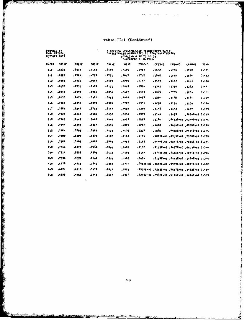
Table Il-i (Continuee)
P~~t3NAII~ *'SECTIO4 MEhNtS-LlkF 7RANSFO9V" E3.0. CR15781.CITA'C- N0WLIZED TO 176.716CWTEPSS
otoum 1971 fAPLhkS * 'a TO 16 08qagiI1Th*S.00/1.
RL/As C61/1 C42/1 C63/1 C@SIE CGS/E C*&12IE C01331 VseE Cwr/ v5vn
loS .332 .7079 *?193 .7149 *4s .1446 .162 .1700 072A .l~
1.1 .33 .644 .0119 .6731 *74o? .170Z .5ss 116 IS6& :.n33
1.t *flat .631 .44 Ga4ns .7p55 .114,Sq 4.~ .4. .4
1.3 .849 .6731 664 .6121 .6oas *1524 -1382 .1318 .135? 1."Pj
1.4 68111 .4395 .6261 .985I .06422 .1413 .13iq .,-SS .1254% 1.1ni
1.5 IBM3 .3474 .075 .9612 .606A .1.2S .2244 .19~5 .1171 1.119
1.3 IMP8 .4354 .5ave .9394 .4772 .13o4 .1ze .1130 .1100 1.13f,
Is? .7594 .6247 S5733 .5"97 .42 .1344 11 .1643 .143? 1.151
t.o .7023 .61*3 .5504 *50406 SPS4 .1319 .1144 .1"39 *9654E-01 1.169
lo9 .7745 .6040 .5448 .4949 Sfk36 .1209 .1149 .9CW3-ol Q37GE-o! 1.iA&
2.8 .7618 S92 .5S20 .4694 .42S .1261 .1078 U!C.1E-02 RI'34E.01 1.194
2.2 .7516 .5702 .5sas .4424 .4475 .1229 .14 1*428E-02 A4161F-81 14224
2.4 .7402 .5GE? .4815 .4185 .4160 .11V4 .9833-01 SS403E-01 .756AE-0' 1.I53
2.6 *7327 .5493 .4390 .3943 .,%OCR .1163 .94"-01 .8037E-01 .7030E-01 1.281
2.0 .7396 .5372 .'5So .3480 .3 .1132 .91W3.01 .763fl-0: .66CIC-01 1.3n&
3*e .7214 .5236 .4391 .3636 01483 .1104 .07031.01 .7112C-01 t4le1-01 1.!,16
US5 .703 .5022 .4107 .33?)r 14 Ines4 .6119E.81 .6463E-01 S5O--o 1-1.76
3.0 41179 .490 .3043 .305 .?776 .Ot44-o1 .74431.01 *5I89E.01 .40W1-01 1.42?
4.5 .6721 .4313 .3017 .2417 .?521 qsz21c-! .?242E-01 SS647E-01 .4463E.01 1.4441
s.0 .4529 .4435 .3441 .24 .732: Sz215z-o1 .69W0.01 .5I96E.01 .4090E01 1.Se,
28

Table II-1 (Continued)
PROGRAM By S SECTInN MFANOER.LINE TRANSFORMER TABLEt*, CRISTAL CAPACITANCES NORMALIZEO 70 316.7/SQRTEPSR)OCTOB 1C71 CftPLl
NO 8 10 70 16 08
RANDOWDTH 8 6.00/1,
mL/'f COiVE CO/E COS/E C04/' CGS/E CM12/E CM23/E Cm34/E C0045/E VSwR
1l. .6171 ,6912 .7200 ,To9 ,0P86 .2071 .1727 .1638 1922 1.00
1.1 0S6SS .6672 o6963 .674S .7703 1986 .156 ,IS45 .1614 1.043
1.2 .027A .6831 .6669 .6434 .7?74 *is?$ .1406 .1424 .1456 1.1)84
1.3 676 .6726 .6491 .6167 ,AASS ,1411 *368 .1317 .1327 1.116
1.4 .076 *'576 .6276 *509n .A461 .14S2 .1316 .1244 *12sp 1.144
1.S .791n .6440 .6081 ,56%? .6136 .1406 ,1259 .1142 .166 1.171
1.6 .704 .6316 .5907 .5456 ,*47 .1361 .12T2 .1127 .o091 1.196
1.7 .76og .6200 .5744 ,S266 ,Srep .1326 .1173 *18O0 1n3l 14220
1.8 .7734 .6093 .5599 .5083 .5334 .1289 .1130 I132 ,984%E-01 1.243
1. .7692 .5994 .5462 .4924 .5122 .1260 .1092 .9961E-01 ,436ME-fll 1.265
3.0 *7561 .5896 .5336 .4773 .423 .1230 .1061 #9603E-01 .9954E-01 1.246
JOE 076J9 .5719 *Sill .014 .4578 .1195 .1066 .8936E-01 .4242E-01 1.321
3.4 .7316 .561 .4903 .4264 ,.?05 .1151 99566E-01 .8457E-01 .759E-01 1;366
2.6 .72 2 0416 .4721 ,.OAn .4036 .1117 .91E-01 *8014E-01 .713M0E01 1.402
.0 .7095 .5263 .4556 .3R95 .3"04 .1045 .8835E-01 ,76IoE-01 .6700SE-01 1.439
3.0 .6996 .5163 .4409 .3731 .3606 ,10s8 .8539E-01 .7305E-01 .635RE-01 1.474
3.9 .6761 .4961 .4104 .3413 *3?11 .1002 .7942E.41 .6572E-01 CS6?E-01 1.554
PPOORAN By 5 SECT1ON MEANOER.LINE TRANSFORMER TABLE
0., CAISTAL C YPAC104NCES NORPALIZEO TO 376.7/SOGRT(EPSR)
OCTOBER 1971 CJUPLINO 0 10 To 16 on
ANOWIDOTH 0 6,40/1.
R%./ms Ce1l COVEI CAVE C042f C05,1E C*.12/t2 C~p'3/f CM34/E cP'4s/E VSWR
10 '6555 .7236 .7300 .7464 .672 ,1590 .17;6 .1496 ,j441 1.400
1.1 08247 .6951 06937 .671S .7732 .1709 .1570 .1S17 .168. 1.o63
1.2 .8236 .60647 .6721 .6474 *714 ,1SST .1436 .1406 .1490 1.114
1.3 .0135 .6683 o6469 .6172 .6*74 .1496 .j3i2 .1337 .135A 1.168
1.4 ,eo16 .6534 .6266 .5932 .652; ,1446 .36 .1.57 ,*j24 1,2is
1.5 ,7906 .6394 .6085 .9717 *620R .1390 .1256 .1166 .1169 1.257
1.6 .7767 .6363 .5917 S520 .5432 .1344 .1194 .1130 .110 1.296
1.7 .7679 .6136 .57sq .5338 .5683 .1303 .11SS .1;81 ,1h64 1.336
1.3 07577 .6018 .611 .5169 .5454 .1267 .1117 .1636 .997?2E01 1.374
l9 .7474 .9965 ,5476 .Se0z .5245 .1239 -1019 .9973E-01 .9S4o" ' 1.411
2*0 .7332 '5798 5345 .467o .O66 .1210 .10011 o96t4E-01 *9116201 1.447
3.0 .722t .56?2 .5126 .4626 .4739 .1156 .9886-01 .9027E-01 .36E3-01 1.S15
29

Table II-1 (Continued)
PACOIAN BY 5 SECTION FANDER-LINE TRANSFORMER TABLEto$* CRISTAL CAPACITANCES NORMALIZEo TO 376.?/SRT(EPSP)OCTOBEN 1471 COUPLINO 8 10 TO 16 Do
RhfIlhOTH a 10,0041,
RLIAG Cal.4 CO2/E C03/E CG4.E C0S/E Cm12/ C23/E CM34/E C44S/E VSWR
1.0 $6476 .7345 .7522 .7532 A677 01602 ,14,2 .1434 .1439 1.000
1.1 .6334 '6989 .6950 .4826 .7851 .1665 .1564 1S05 .1536 1.074
l. 6295 .6160 06694 .6493 *7366 .1538 .i433 .1454 .139A 1.140
1.3 .6092 o6651 .6480 .6225 .6927 ,tS)S .137 *1327 .132A 1,202
1.4 o7913 .0501 .6255 .5944 .AS4; *1441 *1326 -1262 .126; 1.264
1.5 ,7846 .6357 ,6076 .9730 ,t236 .1395 .iW! ,1195 .116 13)
1.6 *7719 .6219 *S900 .S54" .5972 .1346 *12A2 01137 .JllQ 1.373
1.7 ,7596 06087 ,Sq52 .5363 .573A .1303 .Ii, 1os9 .1064 1.425
1.6 .7476 .5961 .5605 *520 .5513 .1267 .1115 .1;46 .1615 10476
1,o .73064 05841 .S464 .5049 ,$317 *1234 @1084 .111 *9703Eo01 1.526
30

''A
.~ ~ ..' . . . . . . .
aa m an I a ap A A A C. 2. 4 - 9 2
U) ~ ~ ~ ~ ~ y v .NaNN2
7 m. m N1 -A vC F. 3 "1 U
U , N N C * 9 N N
a m I 8 IIt
x%- 0 , 0 . cu 'D "1 C ) %on
4* cllc . 2. . . . .' . . . . . .' .
03 .3 c3 . 0 00. -c I 1>I I
* N -£ N- ID I - C N N Nlo CD %n t- %A an - N1 o 4
-a -t 1*4 .3 - l 4 4 -
d* L, aj aD
9d hu In -n - o'9 2 - V 2wo . 2. A) N 2 C * - 'I M 2 03'
0~0
U3UIV)~2 0' 4)- D' M A C )
SN ~~ z I CO *1ofU )4 4 M U
0*t t t
40P.
7.413 _j - - 1 - 1 C C~ - - 41fy 1- L o745 cu
1. 2 2 Rard c d f o0 ZS-13% 23. C9J'Va ava~bl coP9
4 0.2 ) 2 ' N 2.-l C 4 N C 2
0 U)4 . V 4 . ' * 3 -31-
W .j
31
. . . . 3. 3. 3. .
o0 n '- 34 In~-- 3 ' 3
:4 -C Cy In .3 '3
4) r1 33- n - N 3 - Y 4)- - 3 3
7313 ID - U n 0-3. 2 0 - 't- 3' In a a 3 In %, it 3
ca 4
6.4 3 0c ew'34 1 3 ' '3
best avial copya,
-. 33 3 3 .323

S C 4 N C N 5) a. - N P .
in 0l 4 z Cc a 4
n W C. CU C) 43 M CO
cc J u I i
c C a, C uC C L C4- PZC. 5. I. . .' . . . .* 5. '
C C
5., I I S I
Z C'r CC C
c I I a 11 4
a fu m U C N C, .0 .
If) i0 - N - N ' N C C) N 0a'% u a' c Nx A b 5)U----- --- m cNu' 4
-I C Ca, 0
L-U) I- - - - --tC C

0 C C Nu ft n- c0 r- C-C - C N 4 P c39 0 10 - U - - C ' C3 0 P. * w U' a-
w C4 M
N C. U: U. u U. Cfl a 4T #I e Z I. ; I I
t' C' C ' a C OD C M r4 ) U' ' C 4 C- U C C
C4 C C C C
w a I Ia I I
L. w IJ IC ..M' 4 4 C Cf M C C' CY U' C 4' N C
L . .. . .4 .0 .
t "I I CC IC) IC. tr ' w CrU C. C P N 4 ' 4 '. X 4 iP 0 M C
oco .C .C .C .. .C IC...t
ell C' -- - C, C C- 0 C ' - C - - C
P. 4 v C- C' 4 C' w C' -C c a ' U .
WEY IC.-
C ' P 04 U' .0 C- C- a a, I' U' C ' 4 W U' N CU, . M) M 4 i n mC C )I- ~ C' E0 , Q C' & -
2 -
-c C I,Ca-C U, Cc- Iz C a
C~~ ~ .0 Cft0C C U C C 4 -4 en cc C Na ' . ' C vt . CP to~n )c z m44 . '
i-I .c.CI WI. I
a 4 U i CP r' 4 (r a .. ' S
3)4 C 4 C .4 ID U' 1' 4 ' C L C C ' ' ' C U 4 cu
C ~~P P. t' PU 0C N0 C' a ' C U U - C ' C
W:2 IC .
0 C: ICD
( U C-C. 4. U, 0' 4 . U ) U . . . 4 . U ) U
CCqroue FwM --- S 4 4 4 U' CU availabl C' '.S. C C C ' £ '
4034

C C
- n U) - r MtIP 4 M ) a U) 4 U
C, v
i
a c t t -(n U - a n
I. B
ctcLP C r 4 t 0 ft f
- ft it I f tg 4oL C at it C, -a I m
0. C; U)NO)
-, CU kn u
4 U!
LL . c -
B Lc a- C.
1LV4 It - U C P
3B.C~ t. ft C wf at U
LB. In
0 0 U) U) - ft C -
U ft C C i. i)
35 4 i C f

2. Discussion of Design Tables
For the data presented in Table II-1 the coupling between
meander-line turns was arbitrarily (after some analytical experimentation)
required to be within the range 10 to 16 dB. This range of coupling
generally yields a realizable and compact structure for co-planar coupled
strips. Tighter than 10 dB coupling tends to become difficult to realize,
while greater than 16 dB coupling is entering a region that is beginning
to separate the adjacent strips farther than is desirable. Since the
effects of the finite-length intercLanections between strips were
neglected in compiling the Table I1-1, the interconnection lengths should
be made as small as possible, if the measured performance of the trans-
former is to correspond well with the theoretical performance. In the
realization of the transformers, compensation of the interconnections
will generally be required.
The effects of varying the coupling between meander-line turns
are shown in the graph of Figure 11-6. This graph is ior the particular
case of N = 4 turns. RL/RG = 2, and BW = 3:1, but is typical of the
results in the general case. The graph plots maximum VSWR in the pass-
band as a function of coupling between turns. The horizohital arrow
depicts the range of coupling allowed. The right-hand sides of the
arrows are connected by a smooth curve. This is somewhat arbitrary, but
is justified by the fact that coupling values determined by the computer
tend toward weaker coupling in most cases. In any event, the qualitative
result is the same regardless of the way the curve is connected. The
data show that for a given bandwidth the peak VSWR is minimized when the
coupling is weakest. Thus, for the class of meander-line transformers,
stepped-impedance transformers yield the lowest VSWRs. This is not an
especially surprising result, since the coupling between turns introduces
constraints on the physical realizability of the meander line. Also, the
36

1.15 --
I1.14 Coupling Range
1.13
1.12
1.11
1.10
1.09
> 1.08
2 1.07x
E 1.06
1.05 -
1.04N = 4-Turn Meand.r-Line Transformer
1.03 -BW - 3:1
1.02 - RLIRG " 2.0
1.01
1.001 2 3 4 5 6 8 10 20 30 40 50 60 80 100
COUPLING - dBTA-8245-119
FIGURE 11-6 VARIATION OF PEAK ;F-WR FOR VARIOUS COUPLING VALUES BETWEENMEANDER-LINE TURNS
same conclusion might be inferred from the data of Wenzel, 14 #15 which
showed that C-section transiormers* have smaller bandwidths than stepped-
impedance transformers for a given VSWR and number of sections.
Since Table II-1 was developed using numerical techniques,
it is worthwhile to examine the responses of the transformers in some
detail. Figure 11-7 shows typical computed responses for 3- , 4- ,
and 5-turn-mernder-line transformers, all having 3:1 bandwidths, 3:1
* A C-section transformer may also be considered a two-turn-meander-
line transformer.
37

1.50
1.45 BW = 3:1
Banddge 450 Coupling = 10 to 16 dB
1.40 LG 3
1.35
1.30
U 1.25> N 3
1.20
1.15[ 1.10
1.05
1.0040 45 50 55 60 65 70 75 80 85 90
0 - degrees
TA-8245-118
FIGURE 11-7 VSWR vs. ELECTRICAL DEGREES FOR N = 3-. 4-. AND 5-TURN MEANDER-LINE TRANSFORMERS
38

impedance transformation ratios, P:,d 10 to 16 dB coupling between turns.
The improvement in VSWR with increasing N is evident. The VSWRs are
not quite equal-ripple, but, on the other hand, are so close to equal-
ripple that the difference i virtually academic. Certainly, in Lny
realization of these designs, the effect of losses, interconnections,
and parasitics would completely obscure any differerces between these
and precisely equal-ripple designs. Note also that the peak VSWR occurs
at the band edge. * Since it is the peak VSWR that is given in Table If-1,
and since the band edge performance is almost always degraded in actual
hardware realizations, a user may generally assume that the maximum VSWR
is slightly lower than that given in Table II-I over the baind of
application.
Figure 11-8 presents representative data of maximum VSWR versus
bandwidth (BW), with the number of meander-line turns as a parameter.
Also plotted are the corresponding data for stepped-impedance transformers.
The impedance transformation ratio is 2:1 and the coupling between meander-
line turns is 10 to 16 dB. The data show that superiority of the stepped-
impedance transformer with regard to electrical performance. However,
equivalent or improved performance is always possible with meander-line
transformers by adding additional turns. Again, we reiterate that the
principal advantage of meander-line and hybrid meander-line transformers
is the reduction in overall length and the irncreased flexibility in
obtaining suitable shape factors for the stripline or MIC transformers
being considered.
This is not always the case, but is usually so.
39

1.5-
1 4 M 2 2 M3 M4 S 3 5 54 -~ M//.000
1. S24 3 47 - --
*- 1.3
'00- mi. Meander-line (i turrs)
A 7. 00,Coupling - 10 to 16 oaAl 14 ' -'0 -5- S. StePped-Irripedancte (i sertions)
R1 /R .
1 2 3 4 5 6 7 8 9 10
BANDWIDTH RiATIOTA-8245-117
FIGURE 11-8 VSWR vs. BANDWIDTH FOR MEANDER-LINE AND STEPPED- tMPEDANCETRANSFORMERS
3. Example Design
The use of the meander-line-transformer cesign tables (Table II- )
will be illustrated in the following example. It is required to match 25
to 50 ohms over a 3:1 bandwidth. The maximum VS*4? allowed is 1.1.
Checking Table 11-1 lor RIV/RG = 50/25 = 2, and for N = 2. 3, and 4,
shows that the na~imum VSWRs are 1.352, 1.288, and 1.095, respectively.
Thus, N = 4 turns is sufficient. The parameters from the N =4, W 3:1
tables are as follows:
CGl/E = 0.7757
CG2/E = 0.5699
CG3/E = 0.4826
CG4/E = 0.4744 (11-6)
.4 CM12/E = 0.1298
ChI23/E = 0.1041
CYM34/E = 0.09295
40

We will assume that the trausformer is to be constructed in stripline
on l-Oz copper-clad Rexolite 1422. %vhich has a relative dielectric con-
stant of 2.54. Siace the tables are calculated on the basis that the
"load" is always greater than the source, the generator resistance in
this case is identified as 25 ohms. Consequently, substituting Eq. (11-6)
into Eq. (I.-5) (page 9) --ialds
C = 376.7 (0.77571 = 9.454(0.7757) = 7.334g1 25/=54
C = 9.454(0.5699) = 5.388
g2
C = 9,454(0.4826) = 4.563
g3
C 9.- = 9.454(0.4744) = 4.485 (11-7)
C 1/ = 9.454j0.1298) = 1.2-2712
C 23/C = 9.454(0.1041) = 0.9-42
C34/C = 9.454(0.092?5) = 0.8788
Substituting Eq. (11-7) into Getsinger's data yields the results given
in Table 11-2.
C. Experimental Results
1. Three-Turn-Meander-Line Transformer
P three-turn-weander-linE transformer was designed to m-t.ch a
25-chin load to a 50-ohm source over a 60-percent bandwidth (BW = 1.857).
It was constructed in stripline using I-oz copper-clad Rexolite 14122,
and a ground-plane spacing of 0.250 inch. The e.ectrical =nm dioens-onal
41

Table 11-2
EXAMPLE FOUR- TURIN-MEANDER-LINE
3: 1-BANDWIDTH TRANSFORMER DESIGN
(RL/RG = 2)
Conductor w/b* s/b+
1 (25 .. end) 1.550 0.1059
2 1.224 0 1508
3 0.9911 0.1767
4 J0 .g137
* w/b = Strip-width-to-ground-plane
spacing.
t s/b = Interstrip-sacing-to-ground-
plane spacing.
parameters are given in Table 11-3. The nominal center frequency was
I GHz. The interconnections between meander-line turns were miie-ed
experimentally for a satisfactory VSMR. Four 1/b-watt, 100-ohm carbon
Table 11-3
ELECTRICAL AND DIMENSIONAL PARAMETERS FOR AN EXPERI.IMITALSTRIPLINE ThREE-TURN-MEANDER-LINE TRANSFOFRMER
C /A C Linewidth, Inter-LineLine g ii+ w Spacng, s
S (inch) (inch) '
(25-. side) 6.7191 .6u05! 0.354 0.015
2 4.2162 1.5L74 i 0.216 0.018
3 (50-.. side 4.1891 _ 0.196
Impedance transformation 2:1 ITheoretica] VSIR - 1.048
Fractional bandwidth 0.60 (BW = 1.857)1
42

resisters connected in parallel were used for Lhe 25-ohm load. A
photograph of the final design is given in Figure 11-9. The measured
and computed VSW~s are ihown in Figure 11-10. Note that althongh the
center frequency of the transf(rmer is slightly high, and although there
is some degradation in the response near the upper band edge, generally
speaking, there is excellent agreement between the two curves. Also,
a photograph of the measured reflection coefficient from 400 to 1400 MHz
is shown on an expanded Smith chart overlay in F4gure 11-11.
2. Fourth-Order Hybrid Meander-Line Transformer
In order to confirm the theory and design procedure for hybrid
meander-line transformers, an N = 4 hybrid transformer covering a 4:1
bandwidth and matching 25 to 50 ohms was designed. The theoretical VSWR
is 1.14. It was also constructed in striplir., using l-oz copper-clad
Rexolite 1422, and a ground-plane spacing of 0.250 inch. Its nominal
center frequency was 1.250 GHz. The electrical and dimensional para-
meters are given in Table 11-4, and a photograph of the transformer
after the interconnections were mitered is given in Figure 11-12. The
measured data at the high-frequency end of the passband indicate that
the interconnections are not completely compensated; nevertheless, the
mean return loss is about 23 dB. Hence, the correspondence with the
theory is very good.
43

ifl
II
w
x
XU-
icc
0
0 <
CD
I~ ~ -- eProduced /
44

1.7
1.6
1.5
1.4
1.3
1.1
400 500 600 700 800 900 1000 1100 1200 1300 1400
FREQUENCY - MHz TA-8245-124
FIGURE 11-10 MEASURED AND COMPUTED VSWRs FOR EXPERIMENTAL THREE-TURN-MEANDER-LINE TRANSFORMER
45

w OR> cn0oz
ZW
zzw
tLW
LL w
LLw
wo
U
Repoduce frombestavai~b!.copy
46W

Table 11-4
ELECTRIICAL AND DIMENSIONAL PARAMETERS FOR AN EXPERIMENTALFOURTH-ORDER STRIPLI NE HYBRID MEANDER-LINE TRANSFORMER
C C* /e Linewidth, Inter-LineLine 9 ~ + w Spacing, s
(inch) (inch)
1 (25-sl side) 7.208 1.2300 0.380 0.026
2 6.182 0.0 0.316 -
3 5.2792 0.9006 0.253 0.043
4 (50-n, side) 4.*5239 0.206
__________ouce from_ _ __ _
F!GURE 11-12 PHOTOGRAPH OF AN EXPERIMENTAL N =4 HYBRID MEANDER-LINETRANSFORMER
47

0
5 -
10 -
15 1.432
0-Jz
. 20 1.222
.MEASUREDi
25 - 1.119
,,- COMPUTED "
30 - 1.065
35-300 500 700 900 1100 1300 1500 1700 1900 2100
FREQUENCY - MHz TA-8245-123
FIGURE 11-13 MEASURED AND COMPUTED RETURN LOSS FOR EXPERIMENTAL N = 4HYBRID MEANDER-LINE TRANSFORMER
48

III NEGATIVE- IM.IPEDANCE CONVERTERS
A. General
During the final reporting period, two types of negative-impedance
converter (NIC) circuits were designed and constructed: (1) a high-power
NUNIC filter and (2) a FET-NIC filter. A high-power NUNIC filter was
built to show the applicability of the NUNIC design approach to the
realization of large-signal as well as small-signal devices. A FET-NIC
filter in integrated form was built to show that active filters can compete
with crystal filters in stability, bandwidth, and size.
The design and performance of the high-power NUNIC circuit is dis-
cussed in Section III-B, and that of the integrated FET-NIC filter in
Section III-C.
B. The NUNIC Circuit
1. Qualitative Analysis
A description of the operation of the NUNIC circuit, along
with some measured results, was presented in the Semiannual Report 1
on this contract. 1 A high-power filter operating at 230 Mhiz was
designed and built using this circuit because the NUNIC utilizes the
inherent time delayb in high-power transistors and their intercor iections
in order to operate at much higher frequencies than are possible using
conventional NIC circuits. Hlowever, temperature and transistor parameter
sensitivity may be a problem with the NUNIC because the common-emitter
transistor, whose gain is beta-dependent, operates with no negative
feedback. The addition of negative feedback can be easily implemented
49

_ r "_
by inserting a resistor (or more complex load) in the emitter-to-ground
path. This complicates the analysis of the circuit because h 1 is no
longer small and is a strong function of the emitter load. Collector-
to-base feedback in the common-emitter stage is not useful for achieving
negative feedback, for two reasons: (1) Such feedback tends to lower
the output impedance of the common-emitter traisistor, which in turn
increases the sensitivity of the circuit to parameter changes in the
common-base transistor, and (2) unaioidable parasitic effects tend to
make such feedback much less effective at microwave frequencies. There-
fore, negative feedback was applied to the NUNIC circuit as an emitter
load Z , as shown in Figure III-1.
The commen-base stage, because its gain is dependent on alpha
rather than on beta, is much less sensitive to parameter variations.
This is because alpha changes much less than beta with changes in operat-
ing voltage, curreit, and frequency. Consequently, no attempt was made
to add negative feedback to the common-base stage.
(Part 1)
'bl
lel "X 2 PORT 2
TA-8245-125
FIGURE 111-1(a) NUNIC WITH NEGATIVE FEEDBACK-SCHEMATIC DIAGRAM
50

z Vj
GI-
LU
00
-Ji
00
C-,4
~51

The element values for the NUNIC circuit with emitter feedback
were chosen to give the desired impedance function at Port 2 while
maintaining as much negative feedback as possible in the common-emitter
stage. This is accomplished most efficiently by using a computer program
designed to chose element values that minimize the sensitivity of the
input impedance at Port 2 to transistor variations, while still main-
taining the proper impedance nt that port. However, the development of
such a program was beyond the scope of this contract. Instead, the
following procedure was adopted. (Each step will be explained in detail
as we come to it.) One first .zhooses an emitter impedance Z , and thene
tries a series of load impedances Z , from which one computes the input
impedance Z at Port 2. After a series of trial-and-error calculationsin
to obtain the desired Z in' one thus selects the "optimum" Ze and Z --
they are "optimum" in the sense they give not only the desired
Zin , but also low sensitivity to variations in the transistor parameter,
f . Refer to Section 4 for a more explicit design procedure.
It should be mentioned that there is another practical limita-
tion on the magnitude of Z . Since the emitter current of transistor XIe1
flows through this impedance, tnere is a voltage drop across it that may
be considerable. The collector current I of transistor X is approxi-
mately BI b, where Ib is its base current. The emitter current Iel of
transistor X1 is approximately (3 + 1)Ib. At the frequency where the
NUNIC circuit is used, the magnitude and angle of 3 are likely to range
from 2 to 5, and from 140 to 120 0 respectively. Consequently, the
magnitude of the collector current i bI! is generally quite close to the
magnitude of the emitter current l(B + l)Ibl , as is indicated in
Figure 111-2; in symbols, Iel is app-:'ximately equal to I cl. The
collector current of X2 , which is I2* is approximately equal to its
emitter current, Ie2' for the same reason. Referring to
52

TA-8245-127
FIGURE 111-2 PHASE AND AMPLITUDE OF 0 AND 0 + 1
Figure III-l(a), Ic2 is therefore approximately equal to I = Icl ,
hence approximately equal to I el. Now, I and 19 are both
supplied by the collector current of transistor X2, and II and 12
are approximately in phase in order for NIC action to occur. Therefore,
any X 2collector current flowing into I1 is not available at Port 2.
I1 may be decreased by increasing the beta of transistor X I . Thus it is
important that transistor X have as high an f as possible in order to1 t
maximize the power output of the NWC. A second constraint on transistor
X is that it must be capable of handling at least as much current as1
the output transistor, X 2. A third constraint on transistor X is break-
down voltage. An impedance in the emitter-to-ground path of transistor
X has flowing through it a current at least as large as the output current1
I . thus, an emitter impedance comparable in magnitude with the impedance2
seen by the output transistor, X2 , will result in comparable voltage
swings in the emitter of transistor X . Although this results in a large~1
amount of negative feedback, it also means that transistor X1 must have
a voltage-breakdown rating similar to that of transistor X . This require-2
ment is in conflict with the requirement for a high-gain transistor at
X1, be,.ause raising the breakdown voltage of a transistor of given
geometry tends to lower its gaiu. Therefore, voltage-breakdown considera-
tions may limit the magnitude of the emitter impedance of transistor X .
1
53

To recapitulate, transistor X should be a high-f , low-voltage1
device, and transistor X2 should be a lower-ft, high-voltage device.
At the highest frequency of operation the beta of transistor X, would
be chosen to be no less than 2, so that not too much of the output
current from transistor X2 would be lost to feedback. Similarly,
transistor X would be chosen to operate below its alpha-cutoff frequency.2
In a later section, techniques that raise the upper frequency ct which
negative resistance can be generated will be discussed. However, such
techniques will tend to reduce bandwidth.
2. Choosing Transistors
The common-base transistor X2 operates "Class A" and is there-
fore limited in efficiency to less than 50 percent. A power output
capability of 2.5 watts from this transistor requires that it dissipate
at least 2.5 watts at full output. The total dc input of at least 5
watts must be dissipated by the transistor when no input signal is
present. A transistor with internal emitter-balancing resistors is
essential for operation nt this power level. Experience with the
Fairchild MSA 8505 transistor has shown it to be rugged which,
combined with its alpha-cutoff frequency of 500 MHz, makes it quite
suitable. An operating voltage of 20 volts from collector to base was
chosen, to be on the conservative side, and an operating current of
250 mA was chosen because it is approximately in the middle of the
linear operating range of the smaller common-emittar transistor that
was initially used. The MSA 8505 transistor is capable of operation
at 500 mA of collector current if a larger common-,Nmitter transistor is
used.
The common-emitter transistor X can operate with a lnwer
collectcr-emitter voltage than X2 , but it should have an ft of approxi-
mately 1 GHz. For this application, another readily available transistor,
the MT 5764, was chosen together with a backup device, the MT 5765. The
54
current cap-bilities of the MT 5764 a )ea.ed barely adequate; therefore
the slightly-lower-gain MT 5765 capable of nearly twice the cu.'rent
swing was also acquired. The ,iT 5764 is capable of continuous operati.on
with 10 volts from collector to emitter and 2.50 mA of collector current.
It was anticipated that the MT 5765 transistor would replace the smaller
device, once some experience was gained in mounting, heat siiking,
biasing, and stabilizing the trarsistors.
3. Load Impedance and Power Capabili ies
If all the collector current of transistor X was assumed to
flow through the external load at Port 2. then one could easily comput-,
the maximum sinusoidal RF power, PI' availab.e at that port. This power
would be
I•Vc cb
! 2(1-)
which is the maximum undistorted power output from a Class A amplifier
onerating at I collector amperes and V collector-to-base volts.c c
At 23C Hz, nearly 0.2P1 was calcuxated zo be fed back to the base
of the common-emitter tr*ansistor. A higher-gain, more exotic transistor
than the MT 5764 would help to lower this loss, but the attempt here iv
not to wring the last dB of output from tne NUNIC at all cost, but rather
to achieve a practical design with transistors that represent a practical
compromise in ccst-versus-performance at the operating frequency. The
expected undistorted power output from the NUNIC, P, would therefore be0given by:
P 0 0.41 * V . (111-2)0 c cb
* See Ref. 16, p. 36.
55
When the NUNIC is embedded in a one-pole filter, thereby
rendering the filter lossless, the maximum undistorted RF power output
from the filter, P OUT' is given by*
P0
OUT 2QL/Q (Il:-)
The quantity is defined as the loaded Q of the filter with the NUNIC
embedded, and Qu is defined as the Q of the tuned circuit alone, with
nothing else connected.
In a lossless one-pole filter the positive load resistance on
the NUNIC would be R , the parallel-equivalent loss resistance of thep
tuned circuit.T This loss resistance is neutralized by the NUNIC's
negative input resistance to make the tuned circuit effectively lossless.
R , the optimum load on the NUNIC for maximum power output would be givena
Vcb
a 0.81 (111-4)
c
The 0.8 in Zhe denominator results from the loss of 20 percent of the
output current to the feedback loop. For the maximum filter power
capability, R would be made equal to R ain order to naximize the power
delivered by the NU NIC.
Equations ((11-2). (111-3), and (111-4) can now be used to
estcblish the ope~kting condititns and the load for the transistors used
in the high-power NUNIC.
* See Ref. 15, pp. 41-44.
t See Ref. 16, p. 45.See Ref. 16, pp. 35-36.

For example, if the NUNIC is operated at 250 mA of collector
current and with 20 volts from collector to base on the common-base
transistor, then the NUNIC power output, P0 , as calculated from Eq. (111-2)
would be
P = 0.41 V = 0.4 X 0.25 X 20 = 2 watts (+33 03m)0 c cb
The power output from the filter would depend on the relative Q multi-
plication desired. Suppose the NUNIC filter utilizes a tuned circuit
whose unloaded Q (Q ) is 80. If this tuned circuit is used in a filteru
whose loaded Q (Q L) is 85 (2.7 MHz bandwidth at 230 N {z), the maximum
undistorted filter output power, POUT' would be Efrow Eq. (111-3)1:
P. 0 2P 1 - /0 0.94 watt (+29.7 dBm)OUT 2 %/Q u 170/80
Also, the optimum load resistance Ra is found to be [from Eq. (111-4)]:a
V• cb 20R cb 2 - 100 ohmsa 0.81 0.8(0.25)
c
A theoretical basis for tle calculation of intermodulation (IM)
diste-tion in a NUNIC filter has Y et been worked out. An emitter
impeda.rce of 10 or 20 ohms will minimize the distortion generated by the
common-emitter transistor. However, it is likely that the varactor
effect of the collector-base junction of the common-base transistor is
a significant source of IM distortion in the NUNIC, just as it is in
linear-transistor power amplifiers at these frequencies. Replacement
of the MT 5764 by the MT 5765 transistor having twice the current-handling
capability will allow twice the filter power output for the same collector-
voltage swing, with a corresponding increase in the third-order intercept.
57

In addition, R would be decreased to SC ohms, thereby further reducinga
the IM distortion because a smaller fraction of the NUNIC output current
would flow through the varactor and a larger fraction through the increased
load conductance. Therefore, the replacement of the MT 5764 with a MT 5765
should increase the third-order intercept of the NUNIC filter by 6 dB.
4. NUNIC Load and Emitter Impedances
A NUNIC circuit design that will generate -100 ohms at 230 MHz
will now be presented. This wil3 satisfy the specifications of the
previous section and will also neutralize tuned-circuit losses. To
design such a NUNIC circuit it is necessary to compute the input impe-
dance of the NUNIC whose equivalent circuit was shown in Figure III-1(b).
We adjusted Z and Z , as described in Section 11.1, calcu-e 1
lating the input impedance Zin (as a function of both Ze and Z ) until
Z not only equalled -100 ohms but also showed little sensitivity toin*
variations in f • The final element values for the circuit shown in
Figure III-l(b) are given in Table Ill-l, and a negative-conductance
comparison is given in Table 111-2.
A capacitor, C2 , had to be added to the emitter feedback
circuit in order to narrow the frequency range over which the NUNIC
circuit developed negative resistance. This helped to stabilize the
circuit, reducing the tendency to oscillate.
In this calculation the starting point for Z was taken as 25 ohms,because this would give almost unity loop gain; Z was then varieduntil iZin' was a minimum with respect to Z . Ittwas found that IZ Iwas too large, and to reduce it, Z had to e reduced (always looking
for a minimum of IZnI with respect to Z ). Once the desired value ofZ (namely -100 ohms) had been obtained, the alpha-cutoff frequency
(in) of both transistors was varied by ±10 percent, and the effect on
i "Z~n was calculated. Since the sensitivity of 1Z.I to the twowas considered satisfactory, no further changes in Ze and Z were
made. Clearly, there may exist other choices of Z and Z. which will4
further reduce the sensitivity of the circuit to changes in f a
58

Table 1II-1
FINAL ELEMENT VALUES
L 16 nH L 1 nH L 2 nH1b b
1 2
C 1 22 pF Le 1 nH Le 10 nH
R 100 ohms R 1 ohm R 0.3 ohm1 b 1b2
R 1 ohm R 0.3 ohme e
1 2
L 110 nH C 5 pF C 10 pF2 c C21 c2
C2 5 pF oYi 0.98 c2 0.98
R 12 ohms f 2700 f 14002 0' 11 2
Table 111-2
CONDUCTANCE CHANGE WITH f VARIATIONor
f f-G CY CY_GIN 1
0.01022 24C0 1260
0.01032 2700 100
0.01039 3000 1540
59
I

Note that a ±10 percent change in f for both transistors
resulted in a change of less than ±1 percent in the negative conductance
generated by the NUNIC.
5. NUNIC Measurements
Unfortunately, there was insufficient time to replace the
MT 5764 transistor with the larger device, so the following measurements
were all made with only the MT 5764 and the MSA 8505 transistors in the
NUNIC. The collector bias current was thus limited to about 250 mA.
At 230 MHz the third-order intercept and the l-dB compression
point were measured under the following conditions:
Vcb (MSA 8505) 20 V
V (MT 5764) 10 Vce
I (both) 220 to 250 mA (optimum range)c
Q 80u
Bandwidth 2.7 MHz
S85
Two-Tone input Power +8 dBm (for IM test)
(each tone)
The third-order intercept measured +35 dBm, and the output
level for 1 dB compression was +29 dBm. The noise figure was also
measured, but it was necessary to lower the collector current to 30 mA
in order to obtain a 21-dB reading on the available equipment. At 220 mA
the noise figure was unreadably high, prcbably 25 -r 26 dB.
6. Noise Figure
Presently, there are no FETs that operate at 250 to 500 mA of
drain current, and yet have reasonable gain at 400 Wiz. Hence, a bipolar
transistor was used in the common-emitter stage of the NUNIC, with the
60

resulting consequences for noise figure* that were noted in Section III-
B-5, above. This high noise figure occurs because the source impedance
seen by the base of the common-emitter transistor (about 200 ohms) is
more than an order of magnitude larger than the optimum source impedance
for minimum MT 5764 noise figure (about 7 ohms at 250 mA). In this
respect the Arr 5765 operating at 500 mA of collector current should be
even wo-se. The An' 5764 transistor is not a particularly low-noise
device, and it is being operated at a relatively high frequency, so it
is expected that a noise-matched noise figure of around 10 dB would be
obtained from this device at 230 Miz. Therefore, even without adding
in the noise contribution of the common-base stage, a noise figure of
18 to 20 dB could be expected for the bigh-power NUNIC. To this would
be added the noise contribution of the loss resistance of the tuned
circuit, which should result in a noise figure for the complete active
filter of well over 20 dB.
7. Circuit Modifications
For operation over narrow bandwidths, stnne changes can be made
in the NUNIC circuit that will improve its performance if it is used
mostly to generate negative resistance (as, for example, in a filter).
Consider the one-pole filter of Figure 111-3, in which the feedback
from the output of transistor X to the base of transistor X has been2 1
changed from a direct RF feedback to a tapped-coil (or transformer)
feedback, as shown in Figure III-3(a). It is no longer necessary for
the current gain oi transistor X1 to be large in order to prevent loss
of output current. Bpcause of transformer action, the base current I1
fed back to transiFtor X may be larger than the transformer current1
* See Ref. 16, p. 44.
61

I-O INPUT
X 2
2 joOUTPUT
TUNED
Ze CIRCUIT
(a) TAPPED-TRANSFORMER FEEDBACK
L PORT 2
X1(b) REACTIVE-TRANSFORMER FEEDBACK
TA-8245-128
FIGURE 111-3 MODIFIED NUNIC CIRCUITS
62

flowing from the collector circuit of transistor X 2 ZZ and Ze will be
affected by such tapping down, and it may even be possible to eliminate
Z for certain combinations of Z , transistor gain, and transformer2 e
ratio. Since "tapping down" lowers the source impedance seen by the base
of transistor X1, the noise figure of the filter should improve.
The high-frequency performance of the NUNIC may be improved at
the expense of bandwidth by the use of a reactive transformer in the
feedback loop. A shunt inductor from the collector of transistor X2 to
ground and a series capacitor from the collector of X2 feeding back to
the base of X will add a negative transmission phase shift (thus1
decreasing the loop phase shift at high frequencies). At the same
time, the base input impedance of transistor X1 , as viewed by the
collector of transistor X2, is raised. Figure III-3(b) shows this
circuit. It is likely that the capacitor could be absorbed into Z,
or that Z could be eliminated entirely.
None of these circuits has been built and tested, but they
are suggested here to show the direction to be taken in future
investigation.
C. The Integrated FET-NIC
1. Circuit Design
The FET-NIC* filter circuit discussed in this section was
implemented in microwave-integrated-circuit (MIC) form. The schematic
diagram for the MIC realization is shown in Figure 111-4, and a picture
of the MIC substrate in F'gure 111-5. Note that all RF chokes have
been removed from the circuit in order to reduce production cost; the
* See Ref. 16, p. 48.
63
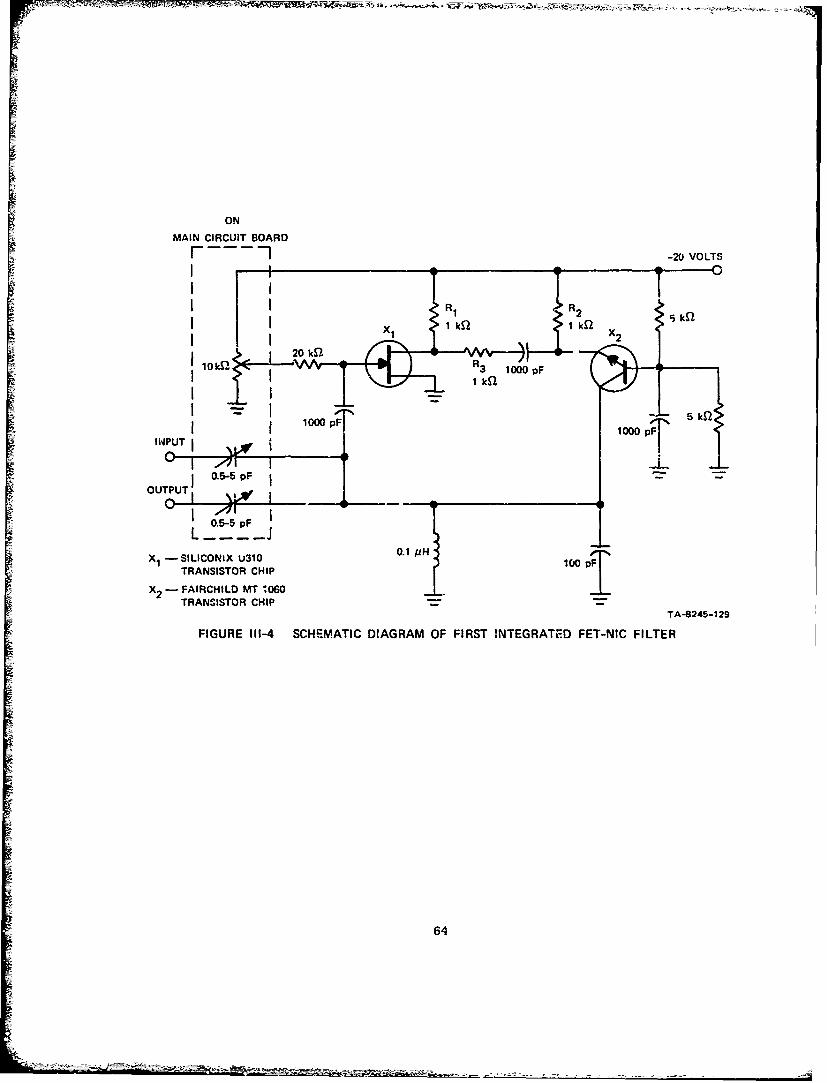
ON
MAIN CIRCUIT BOARD-20 VOLTS
fl~IP TII~j~ iST~ 2 9,~~: kS2
TRNSORP CHIP j -;S
FIGURE~~~~~~ ~~~~ 100-4 pCFAI !GA FFRT NERT FTNCFLE
1649

Rqproduced From01/8 btest available co py.
SCALE - inches
-FIGURE 111-5 PHOTOGRAPH OF MIC REALIZATION OF FET-NIC FILTER
65

PIN diodes have been replaced by a iixed resistor R3, and the variable-
coupling trimmer capacitors are located on the main circuit board
(Duroid material). The 0.1-PH tuned-circuit inductor was initially
implemented as a spiral inductor etched on the substrate. The Q of
this inductor was so low (about 8) that it was decided to replace it
with a ferrite-core toroidal 'Irductor of much higher Q and smaller area.
The only disadvantage o! the ferrite toroid is ' .t the particular
material on hand limited the experimental filter to an operating fre-
quency of 37 MHz because of the rapidly decreasing inductor Q at high
frequencies. However, materials suitable for higher-frequency op3ration
are available. The potentiometer on the main circuit board was an
unnecessary frill, but it was useful for setting the bias on the FET.
The elimination of the RF chokes should have a harmful effect
on the power-handling ability and the noise figure of the active filter.
This can be deduced from the low-frequency equivalent circuit of the
FET-NIC filter as shown in Figure 111-6. The Kirchoff equations for
the loops in this circuit are:
I 2[R + (I - )R = (I - I2)R2
(II - I3)R1 = 3R3 + (I3 - 12)R 2
~1 V = -+ (I 1 - I)R 1gate 11 1 3 1
gm
V : I Rgate 2 p
I2
Solving for , one obtains
1
I RIR2 12
1 [R+ R +R [R + (1 - a)R + R R2
1 2 3 e b 2 2
66

0
GATE
gm SOURCE R3 EMITTER Re COLLECTOR
I13 12 e le
J loss)DRAIN
TA-8245-131
FIGURE 111-6 EQUIVALENT CIRCUIT OF FET-NIC
However, since R1, R2, and R3 are about 1 kilohm, while R and Rb are3 e b
about 5 ohns, one may make the approximation that R2 + Re + (1 - c?)R b -
R2. TherEof oro,
I R2 * 1II RI +R *3 1-5
Thus, a large fra.ction of the current I is shunted to ground by the
1P
decoupling resistor RI, unless R1 can be made much larger than R3
This is impractical because of power dissipation. In the first inte-
grated FET-YIC, R1 and R3 were about equal; therefore, only half of the
RF source current from the FET flows into the emitter of the bipolar
transistor. ;n this case the current swing of the FET will liwit the
power output of the active filter, because the FET and the bipolar
transistors are biased to draw about 8 niA each.
In ..ddition, the noise figure of the filter will suffer because
only half of the signal current from the FET will reach the emitter of
the bipolar transistor. Therefore, some way of eliminating the decoupling
loss was essential for the second integrated FET-NIC.
-67
RANBS

The integrated FET-NIC operated at a slightly higher current
than the first non-integrated FET-NIC, which would have increased the
power handling capability of the FET-NIC filter by 1.5 dB. However,
the decoupling loss of 6.7 dB resulted in a calculated net decrease
in power-handling ability of 5.2 dB. The measured power-handling
capability of the integrated FET-NIC was only 4 5 dB less than that of
the non-integrated FET-NIC. Thus, the first integrated FET-NIC
performed close to expectations.
2. Circuit Redesign
The relatively large microminiature coupling trimmer capacitors
were replaced by tiny Siliconix B7140 varactor chips. The NPN bipolar
transistor was replaced by a PNP device, which made possible the complete
elimination of the coupling loss previously experienced in resistors R1
and R . This PNP device was a Fairchild 2N4957 chip designed for small-2
signal 450 MHz RF amplifier applications. The circuit was made rather
compact, so that a realistic eslimate could be made of the degree of
miniaturization possible with tLese techniques. Figure III-7(a) shows
a schematic of the redesigned FhT-NIC filter and Figure III-7(b) shows
the substrate layout.
The measured performan.,e of the redesigned integrated FET-NIC
indicated that no electrical sacriL -s necessary for miniaturization.
At a comparable percentage bandwidth the newest integrated FET-NIC was
esscntially identical in performance to the lumped-circuit FET-NIC
reported previously (see Section TII-D). In addition, the bandwidth
of the integrated filter could be electrically varied from 0.2 to 1.4
percent.
* See Ref. 16, r 48.
68

Xi - SILICONIX U310TRANSISTOR CHIP
X2 FAIRCHILD 2N4957
TRANSISTOR CHIP
V1 , V2 -SILICONIX BVI40VARACTOR CHIP +28 VOLTS
5.3 kp001 T8.2 kS2
850 2 X
8.8 kl?t 0 S
51
. S
:E T 5-7 klj
IN U V1 V2
INda I " L w OUTPUT
1000 pF
BANDWIDTHCONTROLVOLTAGE
(a) SCHEMATIC TA-8245-13?
FIGURE 111-7 SCHEMATIC DIAGRAM AND SUBSTRATE LAYOUT OF SECOND INTEGRATEDFET-NIC FILTER
69

> I
700

D. Final Results
In Table 111-3 the new integrated FET-NIC and the high-power NUNIC
are compared with the first FET-NIC circuits and the trial NIC of 1970.
Table 111-3
NIC FILTER PEPx'ORAIANCE
Bandwidth TotalPower Outputjand Noise Third-Order Variationl-dB
Center Figure Intercept in Gain,
Frequency (dB) Compression (dBm) 250C to 60PC
(M{z) I (dB)
Trial
NIC (1970)* 0.6 and 50 17 -20 -1' 5.2
1st FET-NICT 0.6 and 50 7 - 10 +9 +20 0.9
Improved
2nd FET-NICt 0.6 and 50 7 - 10 +12 +23
Ist Inte-
grated FET-
NIC 0.6 and 50 9 - 12 +5 +15 0.9
2nd Inte-
grated FET-
NIC 0.6 and 50 6 - 7 +12 +23 0.9
High-Power
NUNIC Filter 2.7 and 230 >21 +29 +35 0.8
* Source: Ref. 17, p. 51.
Source: Ref. 16.
" Not yet measured.
71

- -F-- -1
IV SLOT LINE
A. General
The idea of using slot line to realize transmission and resonator
elements in microwave integrated circuits was originally described in an
earlier report in this series,l a.d has been treated theoretically in
a sequence of reports since then ,.7,is2. This study has now been
brought to a close, and its last topics are contained in the following
section.
Numerous additional papers and reports on slot-line subjects have
22-27263been published by SRI and USAECOM personnel, as well as by others. 2b- 3
These cover many theoretical, experimental, and application aspects of
slot line. Practical use of slot line appears particularly promising for
ferrite phase shifters, hybrid junctions, mixers, frequency multipli,:Ls,
amplifiers, etc. In most of these applications, slot line would be used
in conjunction with microstrip line to achieve results not possible with
the latter alone.
The basic slot-line configuration is shown in Figure IV-l, and a
sandwich-slot-line cross section is shown in Figure IV-2. Their wave-
length and impedance parameters have been analyzed with parallel electric
or magnetic wall boundaries1 7'19'2 2 and with rectangular shields.1 '1 7
Formulas for their E- and H-field distributions have been derived.ll 20,z,
Wideband transitions to coaxial line and microstrip have been analyzed
and shown to bc practical.21
Preceding page blank
AA
• '- 73
-4*'-

w
I-"
SLOT METAL COATING
d
DIELECTRICSUBSTRATE TA-6884-2R
FIGURE IV-1 SLOT LINE ON A DIELECTRIC SUBSTRATE
I IELECTRIC
ORMAGNETIC
WALL d
'r = /Ur
1
TA-8245-27
FIGURE IV-2 SANDWICH-SLOT-LINE CROSS SECTION WITH A PAIR OF ELECTRICOR MAGNETIC WALLS
74

In this section, two additional aspects of slot lines are treated.
These are four-layer symmetrical sandwich slot line, and coupling between
a parallel pair of slot lines. Because the former is especially intcrest-
ing for ferrite phase shifters, the analysis allows the scalar relative
permeabilities to differ from unity. In addition to obtaining formulas
for Z 1 v/v , and XI/X, the magne'ic-field-strength components in theoe g
various layers are evaluated. Graphs of these allow the choice of
favorable iets of parameters for best phase-shifter performance. A
method of computirg coupling between parallel slot lines is given, and
several curves of coupling and directivity versus frequency are shown.
B. Multilayer Sandwich Slot Line
Figure IV-3 shows the multilayer slot-line configuration that will
be treated in this report. For the computations, b was selected large
enough so that wall proximity effects would be negligible. (Generally,
b > 1.5X is sufficient.) In that case, either electric or magnetic
walls at y = ±b/2 would yield the same results. Magnetic walls were
chosen for the analysis because they lead to simpler formulas and compu-
tation. If electric walls are desired, the approaches of earlier
reports s '192 may be used to make the necessary changes in the
formulas. Electric walls may also be added at z = x(d + d2 + V2 to
surround the multilayer sandwich slot line by a rectangulir electric-
wall shield. This modification can a carried out as in earlier cases
of shields around singlL-substrate slot line and double-substrate
sandwich line. 16 1 7 In addition, the same principles may be used to
treat any number of substrate layers beyond thc total of four considered
in this report.1 7
75
%-------

CC,.
~ N
.. . I..... ....
i X .1*Y
. . ... . .z
-j <. . . ....w N r
- v-
.j .........
X . . .. .. .
. ...................
%%4 ... ......
... .. ......w. . ... ... ..LLI ... ... .... .... .U.
0
76

Formulas for the configuration in Figure IV-3 were obtained by a1I6-2,2
straightforward extension of the previous analyses. The total
normalized susceptance at z = 0 looking toward the right and left must
be zero, as follows:
2u11 1 80 = t p - - + (IV-l)
tp 2 F
22pF 1nl
6rl tanh r n coth qn
ra r1 2 sin 2 n6
n=1/2,3/2,... [i (- i 1 (rn6)
Notation for dimensions, permeabilities, and permittivities are indicated
in Figure IV-3, while X' = slot-line wavelength, 1 = 376.7 ohms per
square, and 6 = w/b. (Note that r and pr are scalar quantities.rl r2
Nonisotropic and nonreciprocal effects are neglected.) The value of
p satisfying B = 0 is p = X/I . Other parameters are:t
r = y nld 1+ rtan lFn 2 tanh n2d2 + tanh rFn (IV-2)
q = Yn d 1 + coth " {Irn12 coth d + cothl Fn'r2) (IV- 3)
v = , u = V rr 2
1 rl rl(IV- 4)
u 2¢ 2
u 2 r2r2
77

-' --¢d %- = o - -- =
F n , F = -
\nX'p/\X'p
(IV-5)
n22n2V\:, -"/
2iun 2,tn 2mnS -bF y = - F ,2ym F . (IV-6)n b n nl b nl n2 b n2
In evaluating Eqs. (IV-1) through (IV-6), care must be taken to make the
correct changes in the various functions when their arguments are
imaginary. 17,1 ), 2
A oimilar extension of the earlier analyses 1 - 22 was carried out
by W. Mohuchi of Sedco Systems; Inc., differing in that p rl = I and
electric walls were used in place of magnetic valls.3 3 The two sets
of equations agree when these minor differences are reconciled.
The characteristic impedance defined in terms of power flow and
voltage V0 across the slot is given by'9 ,22
X, v ApS376.7 ohms (IV-7)Z0 767 k g - t
where LAT is computed from Eq. (IV-l) with X' held constant and p
incremented slightly about the vqlue p = X'/X at Tt = 0. The ratio
of phase velocity to group velocity v/v isg
v f A(X/X')v- 1+ (IV-8)g X/X' d
- -~ -- -7;

In this case L(X/X') and 6f are computed from two separate solutions of
Bt = 0 for two slightly different values of X' incremented about the
desired X'. The value f may be assumed to lie midway in the Af interval.
A time-shared computer program in BASIC language was prepared to
compute X'/X, v/v , and Z0 versus the various parameters at specifiedg0
frequencies. This program was used to evaluate values of X'/X needed
in the field-component computations.
Formulas for field computation have been derived for the multi-
layer sandwich-slot-line cross section of Figure IV-3. These apply in
the z 0 region; however, in the z < 0 region tht-y also apply when the
sign of H is reversed. If the sandwich is symmetrical, H is ne..essarilyx x
zero at z = 0. The field components are expressed as infinite summations
of the individual TE- and TM-mode components with respect to z-axis
propagation.
Formulas for the complete set of six E and 11 components were given
in Refs. 21 and 22 for single-substrate slot lirie and a double-substrate
sandwich. The work has now been extended to the case of multilayer
configurations. The H and H components are as follows, wih thej(wt-2 "tx/X') x Z •
factor e suppressed:
* rhis factor implies wave propagation in the +x direction.
79

* First substrate, 0 z d,
J 2V 0 2.F\ Fni sin m6 2 miyHxTEn TI ~,Prn gnl b
(IV- 9)
1 + (b/nX')2
T -.j2V0 ri sin m6S 2miyH b -cs
xThn T X nF nl mb
(IV- 10)
jtanh rn cosh Y~z-sinh 'Ynll
L1 + (b/nX) 2
oD 2V0 X sin n6 2myH - -Cos -zTEn T bp rlX miS b
[cosh yl z-coth q nsinh y lzi
*Second substrate, di f. z :5- dl + d2
02r 01H - ~HxEn LxEnJ
1-d (IV- 12)
[coshy zdl)-tanh q sinh y 2(z-d,)]Yn2( 1a n
80
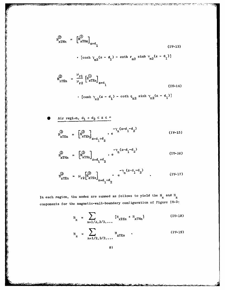
0 [cosh '2(z - dl ) - coth r n2 sinh v n2(z d dl)
H T~n LH T~in1z(I- 3
. [cosh Nn2(z - d ) - coth qn2 sinh n2(Z - )
Air regiun, dl + d2 -z<
-Y(Z-dl-d 2 1[llx T n ] .e(IV-5
HTEn r En 1d+d2
jn = 2) e-yn(z-dl-d 2)-61n] • e (IV-14)* xAT xri zind, +d2
-yn (z-dl-d2 (IV-17)H TEn = TEJ z=d+d 2
r12
In each region, the modes are summed as follows to yield the H xand H
components for the magnetic-wall-boundary configuration of Figure IV-3:
H = E [H xTEn + It xTN-1n ] (V-IS)
Sn=1/2,3/2,.•.•.
[ 0 1n 12(IV-19)
HI = 2:zTEn •Z n=1/2,3/2,...•
81

The variables r n , q n Fnl, etc., are defined by Eqs. (IV-2) through
(IV-6), while rn2 and qn2 are:
rn2 = y, d2 + tanh-l( )2 (IV-20)
= y 2 d2 + coth -- 2) . (IV-21)qn22
A computer program in BASIC language was prepared yielding H and H inx z
all regions. The P , E , Ey: and E components can be obtained fromy x y z
Eqs. (IV-9) through (IV-19) by straightforward use of Maxwell's equationb;
however, for ferrite-substrate devices, H and H in the principal planex z
y = 0 are of primary interest.
Derivation of the mode-summation formulas, Eqs. (IV-9) through
(IV-19), was based on the simplifying assumption of constant E fieldy
across the slot. When w is small compared to b, disregarding the true
variation of E causes negligible amplitude error for low-order modes,Y
but eypreciable error for high-order modes. As a result, the field
.ponents are predicted with excellent accuracy at distances from the
,lot greater than about one slot width, while very near the slot the
error is quite large. In an earlier report1 6 quasi-static formulas
were introduced that yield good accuracy in the vicinity of the slot.
For symmetrical sandwich slot line these are as follows, on the z axis
between z = -d and z = d:
12 01 2H sinh, j] d
0 Ti_ rdl l (IV1-22)
HS _t z -I dl (IV-23)
82
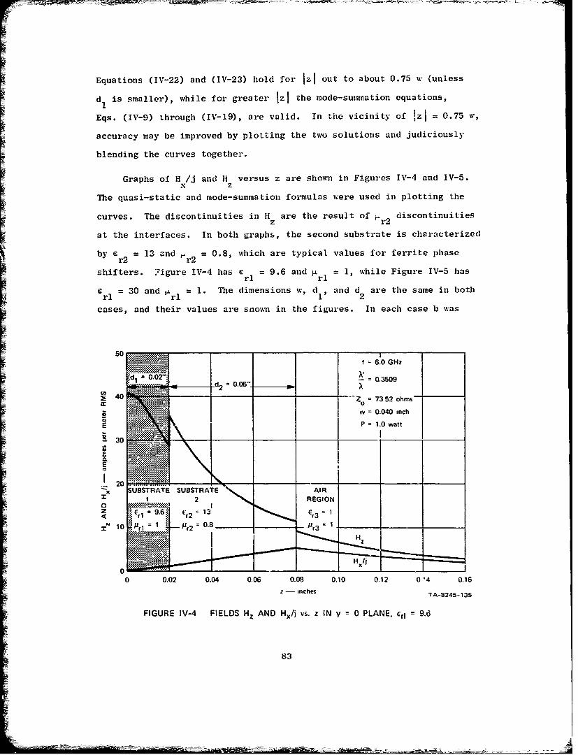
Equations (IV-22) and (IV-23) hold for Iz1 out to about 0.75 w (unless
d1 is smaller), while for greater Jzj the mode-summation equations,
Eqs. (IV-9) through (IV-19), are valid. In the vicinity of 1zJ = 0.75 w,
accuracy may be improved by plotting the two solutions and judiciously
blending the curves together.
Graphs of H /j and H versus z are shown in Figures IV-4 and IV-5.x z
The quasi-static and mode-summation formulas were used in plotting the
curves. The discontinuities in If are the result of. discontinuitiesz r
at the interfaces. In both graphs, the second substrate is characterized
by er2 = 13 and .r2 = 0.8, which are typical values for ferrite phase
shifters. igure IV-4 has e =9.6 and ii 1, while Figure IV-5 hasrl rl
30 and l = 1. The dimensions w, dl, and d are the same in both
cases, and their values are snown in the figures. In each case b was
550 f = 6.0 GHz
- = 0.3509. . .......... d2 =0.06". X '
40 '.. = 73 52 ohms
w - 0.040 inch
E P = 1.0 watt
a30E
x SUBSTRATE SUBSTRATEZ1 2 REGION
S32r 1
1 0 ./ l = 1 P- / , 2
= 0 -8 / r 3 1 .
0 0.02 0.04 0.06 0.08 0.10 0.12 0 '4 0.16
z - inches TA-8245-135
FIGURE IV-4 FIELDS Hz AND Hx/j vs. z MN y = 0 PLANE. crl 9.6
83

60 0.06=02d. f = 6.0 GHz2I
- = 0.2372
Z° = 62.00 ohm
w = 0.040 inch
SP = 1.0 watt
40
E i
'SUBSTRATE SUBSTRATE AIRx 1 2 REGION
o 2 0 E . -Cr = 13' 6r3 - 1
j 1 Pr2 -0.8 r3 =
H
0 ' I
0 0.02 004 0.06 0.08 0.10 0.12 0.14 0.16
z - inches TA-8245-136
FIGURE IV-5 FIELDS Hz AND Hx/ vs. z IN y 0 PLANE, Cr1 = 30
about 1.5 t", which is large engh so that the magnetic walls have
negligible effect on the computed data. Values of X /X and Z0 obtained
from Eqs. (IV-l) through (IV-8) are also given in the figures. The
frequency is 6.0 GHz, and the field strengths are in amperes per meter
rms for one watt of power ilow. This power normalization was obtained
by letting V0 = /27 volts rms across the slot.0 0
Inspection of Figures IV-4 and IV-5 shows that C has a majorrl
effect on the magnitude of H /j in the substrates. A large value ofx
Cr1 yields a relatively large If /j in Substrate 2, which is a favorable
condition f.)r ferrite reciprocal phase shifters. The case of C = 9.6rl
84

Equations (IV-22) and (IV-23) hold for 1z1 out to about 0.75 w (unless
d 1 is smaller), while for greater JzJ the rrode-summation equations,
Eqs. (IV-9) through (IV-19), are valid. In the vicinity of IzI = 0.75 w,
accuracy may be improved by plotting the two solutions and judiciously
blending the curves together.
Graphs of H i'j and If versus z are shown in Figures IV-4 and 111-5.x z
The quasi-static and mode-summation formulas were used in plotting the
curves. The discontinuities in H are the result of discontinuities
at the interfaces. In both graphs, the second substrate is characterized
by 4- = 13 and " = 0.8, which are typical values for ferrite phaser2 r2
shifters. Figure IV-4 has . 9.6 and 1, while Figure IV-5 hasrl rl
= 30 and - = 1. The dimensions w, el and d are the same in bothrl rl 1' 2
cases, and their values are shown in the figures. In each case b was
50 . I - 6.0 GH;a
d1 =0.02" = 03509............._ d2 0 006"- X
40 . -.. .Z = 73.52 ohms
vv = OC. 3 inch
E r = 1.o wat
30 &I.-MA
.44
0E " .... . ..
20S UBSTRATE SUSRTE
0 0.02 0')d 0.06 008 010 0 12 04 0.16
- inches TA-824-135
FIGURE IV4 FIELDS H2 AND Hx/J VS. Z IN y : 0 PLANE, ri 9.6
83

yields almost zero H /j in Substrate 1. In fact, Eq. (IV-22) shows thatx
I /j will be negative in Substrate 1 when 6 t < (X/X )2 . Examples inx rl rl
which this occurs were computed, showing that H /j versus z crossesx
zero at a point within Substrate 2 and is positive thereafter. Tventy-
seven sets of H and H /j versus z were computed with i.r = 1,r2 =Z x
= 13, w = 0.040 inch, and f 6.0 Giz, and with all combinations ofr2
r = 9.6, 13, and 30; d = 0.02, 0.03, and 0.04 inches; and d = 0.02,rl 12
0.06, and 0.10 inches. The computer printouts were furnished to Sedco
Systems, Inc. to aid their USAECOM-supported program on slot-line phase
shifters. Plots of the 27 cases are included in their latest report. 3
These substantiate that a large value of e in the dielectric substrate
1 is needed to vchieve high H /j in the ferrite substrate 2.
x
C. Coupling Between Slot Lines
Coupling between a pair of parallel slot lines on the same substrate
will be treated in terms of even- and odd-mode characteristic impedances
Z , Zo, and wavelengths Xe, X. For weak to moderate coupling, theseoe 00e
can be computed from solutions already available.
Figure IV-6(a) shows the single-substrate slot-line cross section
previously analyzed.1 9 The configuration is bounded by a pair of
parallel electric or magnetic walls with spacing b. For b about 1.5 X'
or greater, these walls have negligible effect on slot line Z and0
while for smaller b these values are increasingly perturbed as b is
decreased.
Images in a pair of electric walls yield the equivalent even-mode
infinite array of Figure IV-6(b), while a pair of magnetic walls yields
the odd-mode infinite array of Figure IV-6(c). Note that the slot voltages
are codirected for the even mode and alternately directed for the odd mode.
We will define Z and ' for the electric-wall, even-mode cases as Z
0 E
85
I !4

ELECTRIC OR -w- -MAGNETIC WAL--,. "
(a) SLOT-LINE CROSS SECTION SOLVED IN REF. 19
lb) INFINITE ARRAY OF SLOTS, EVEN-MODE CASE
-bl
(c) INFINITE ARRAY OF SLOTS, ODD-MODE CASE
(d) PAIR OF COUPLED SLOTSTA-8245-137
FIGURE IV-6 BASIC SLOT-LINE CROSS SECTION, EQUIVALENT INFINITE ARRAYS,AND COUPLED SLOT PAIR
86

and E' and for the magnetic-wall odd-mode case as Z and TheseE At At
may be computed by the formulas of Ref. 19. The symbols Z and X' will0
be applied to the limiting case Z -4 Z Z and V - V as bE At 0 E At
When b is chosen such that ZE, Zh1, and XE, XA are perturbed by relatively
small amounts from Z and V', computation shows these perturbations to0
be opposite pairs:
Z Z +2AZ , Z Z -26Z (IV-24)E 0 M 0
. ' +2AX' , V V -2AN' (IV-25)E At
where
1AZ = -(Z Z) (IV-26)
4 E At
4 ( (IV-27)4 E A
The case of a pair of coupled slots with center-to-center spacing b
is shown in Figure IV-6(d). Each slot has close proximity to one adjacent
slot, while in the infinite arrays each slot has close proximity to two
adjacent slots. Therefore, when b is sufficiently large that the perturba-
tions are small, the even and odd parameters of the pair of slots (Zoe
Z X' X') are perturbed by half the amounts of the infinite array:00 e 3
Z Z +AZ Z Z -AZ (IV-28)oe 0 00 0
X ' + A,' , X V - AX' (IV-29)e o
where AZ and AX' are given by Eqs. (IV-26) and (IV-27).
87
M

= 1q
For an input-wave amplitude of unity, the various output-wave
amplitudes are as follows for Figure IV-7:
C = (t -t (IV-30)2 e o
t (t t (IV-31)2 e o
i (p - p (IV-32)2 e 0
PP+p ) (IV-33)p 2 e o
where p eand t are the voltage reflection and transmiission coefficients
of a length of transmission line with parameters Z oeand cpwhile poe e o
and t are the same but with Z and c0 00 T
* ~ ~'e ~o
zo4--Cz
-t 1
Pz 0
oe 00o TA 245-138
FIGURE IV-7 EQUIVALENT CIRCUIT OF COUPLED SLOT LINES
881

The ineq~uality of cp and cp for a pair of coupled sliots causes
predominant forward coupling. Let coupling and directivity be defined
as followf9:
C =20 log Icj dB (IV-34)10
D =20 log dB .(IV-35)10 i
CArves of C and D versus f were computed and plotted in Figure IV-8 for
=16, d 0.050 inchi, w =0.020 inch, i=1 inch, and b =0.25, 0.35,r m
and 0.5 inch. Junction effects are ignored, and will strongly affect the
mleasured directivity of a practical coupler.
40
30b -O.M."
0
-10
F -20
CL-30
02 ~~~ 33556 "
f -30A-25-3
FIUR V- CULIG N DRETVIY s FEQECYFO05PIRO CUPESLOTS20
-40 1.0
-5089

V CONCLUSIONS
A. Meander-Line ard Hybrid Meander-Line Transformers
A table of meander-line transformers having 2 to 6 turns, impedance
transformation ratios of from 1.1 to 20, ond bandwidth ratios of from
?.5:1 to 10:1 was presented. The transformer responses are, for all
practical purposes, equal-ripple responses. For a given ripple, the
bandwidth of meander-line transformers is less than what can be obtained
with stepped-impedance transformers of the same degree of complexity.
However, the p,'incipal advantage of meander-line transformers is their
compactness.
The concept of hybrid meander-line transformers was introduced.
Hybrid meander-line transformers permit circuit designers considerable
flexibility in choosing the geometrical shape of the transformer design.
The bandwidth of hybrid transformers lies between that of meander-line
and stepped-impedance designs for the same passband VSIR. Several
examples of hybrid transformers were illustrated in the text.
Experimental three-turn meander-line and N = 4 hybrid meander-line
transformers were designed and constructed in stripline. The experi-
mental data agreed extremely well with the theoretically computed
responses.
B. Negative-Impedance Converters
It has been shown that active filters can be built to operate at
power levels above 1 watt at UHF frequencies. In addition, negative
feedback can be used to stabilize these filters so that changes in
Preceding page blank91
operating conditions have little effect on the filter performance.
Although care must be taken with large transistors to prevent spurious
oscillations, one-watt active filters are now practical for operation
up to 1 or 2 GHz.
The FET-NIC can be used to make filters that are stable, low-noise,
3and tiny (less than 0.2 cm3). These filters can be made variable in
both bandwidth and center frequency. A 1.2-percent-bandwidth, one-pole
filter would have typically a 7-- to l0-dB noise figure, +12 dBm power-
handling capability, and a +23 d3nm third-order intercept.
C. Slot Line
Symmetrical four-layer sandwich slot line appears bette. suited
for ferrite-phase-shifter use than a two-layer all-ferrite covfiguration.
The outer layers should be ferrite material, and the inner layers
dielectric material. The use of high- rather than low-permittivity
dielectric material results in far more favorable magnetic-field dis-
tributions in the ferrite layers.
Two parallel slots couple to each other predominantly in the for-
ward direction. The formulas in this report are valid for moderate and
weak couplings. The curves show that good directivity may be achieved
in certain frequency bands.
92

REFERENCES
1. G.L. Matthaei, L. Young, and E.M.T. Jones, Design of Microwave
Filters, Impedance-Matching Networks, and Coupling Structures
(McGraw Hill Book Co., New York, N.Y., 1964).
2. R.E. Collin, "Theory and Design of Wide-Band Multisection Quarter-
Wave Transformers," Proc. IRE, Vol. 43, pp. 179-185 (February 1955).
3. H.o. Riblet, "General Synthesis of Quarter-Wave Impedance
Transformers," IRE Trans. on Microwave Theory and Techniques,
Vol. MTT-5, pp. 36-43 (January 1957).
4. L. Young, "Tables for Cascaded Homogeneous Quarter-Wave Transformers,"
IRE Trans. on Microwave Theory and Techriques, Vol. MTT-7, pp. 233-237
(April 1959).
5. H. Ozaki and J. Ishii, "Synthesis of Transmission-Line Networks
and the Design of UHF Filters," IEEE Trans. on Circuit Theory,
Vol. CT-2, pp. 325-335 (December 1955).
6. G.L. Matthaei, "Short-Step Chebyshev Impedance Transformers,"IEEE Trans. on Microwave Theory and Techniques, Vol. MTT-14,
pp. 372-384 (August 1966).
7. P.N. Butcher, "The Coupling Impedance of Tape Structures," Proc.
IEE, Vol. 104, Pt. 8, pp. 177-187 (March 1957).
8. J.T. Bolljahn and G.L. Matthaei, "A Study of the Phase and Filter
Properties of Arrays of Parallel Conductors Between Ground Planes,"
Proc. !RE, Vol. 50, pp. 299-311 (March 1962).
9. H.S. Hewitt, "A Computer D igned 720 to 1 Microwave CompressionFilter," IEEE Trans. on Microwave Theory and Techniques, Vol. MTT-15,
pp. 687-694 (December 1967).
10. R. Sato, "A Design Method for Meander-Line Networks Using Equivalent
Circuit Transformations," IEEE Trans. on Microwave Theory and
Techniques, Vol. MTT-19, pp. 431-442 (May 1971).
93
L4
11. P.I. Richards, "Resistor Transmission-Line Circuits," Proc. IRE,
Vol. 36, pp. 2i7-220 (February 1948).
12. J.A. Bandler, "Optimization Methods for Computer-Aided Design,"
IEEE Trans. on Microwave Theory and Techniques, Vol. MTT-17,
pp. 533-552 (August 1969).
13. W.J. Getsinger, "Coupled Rectangular Bars Between Parallel Plates,"
IRE Trans. on Microwave Theory -nd Techniques, Vol. MTT-lO,
pp. 65-73 (January 1962).
14. R. J. Wenzel, "Small Elliptic-Function Low-Pass Filters and Other
Applications of Microwave C Sections," IEEE Trans. on Microwave
Theory and Techniques, Vol. MTT-18, pp. 1150-1158 (December 1970).
15. G.I. Zysman and A. Matsumoto, "Properties of Microwave C-Sections,"
IEEE Trans. on Circuit Theory, Vol. CT-12, pp. 74-82 (March 1965).
16. E.G. Cristal, A. Podell, and S.B. Cohn, "Microwave Active Network
Synthesis," Semiannual Report 1, SRI Project 8245, Contract DAAB07-
70-C-0044, Stanford Research Institute, Menlo Park, California
(October 1971).
17. E.G. Cristal, D. Chamber, S.B. Cohn, and A. Podell, "Microwave
Active Network Synthesis," Interim Report, SRI Project 8245,Contract DAAB07-70-C-0044, Stanford Research Institute, Menlo
Park, California (November 1970).
18. E.G. Cristal, D.K. Adams, R.Y.C. Ho, and S.B. Cohn, "Microwave
Synthesis Techniques," Annual Report, Contract DAAB07-68-C-0088,
SRI Project 6884, Stanford Research Institute, Menlo Park,
California (September 19"8).
19. R.Y.C. Ho, D.K. Adams, S.B. Cohn, and E.G. Cristal, "Microwave
Synthesis Techniques," Semi-Annual Report 1, Contract DAAB07-68-C-
0088, SRI Project 6884, Stanford Research Institute, Menlo Park,
California (May 1969).
20. E.G. Cristal, R.Y.C. Ho, D.K. Adams, S.B. Cohn, L.A. Robinson, and
L. Young, "Microwave Synthesis Techniques," Final Report, ContractDAAB07-68-C-0088, SRI Project 6884, Stanford Research Institute,
Menlo Park, California (November 1969).
94
21. D. Chambers, S.B. Cohn, E.G. Cristal, and L. Young, "Microwave
Active Network Synthesis, "Semi-Annual Report, Contract DAAB07-70-C-0044, SRI Project 8245, Stanford Research Institute, Menlo
Park, California (June 1970).
22. S.B. Cohn, "Slot Line on a Dielectric Substrate,' IEEE Trans. on
Microwave Theory and Techniques, Vol. MTT-17, pp. 768-778 (October
1969).
23. E.A. Mariani, C.P. Heinzman, J.P. Agrios, and S.B. Cohn, "Slot
Line Characteristics," IEEE Trans. on Microwave Theory and Techniques,
Vol. MTT-17, pp. 1091-1096 (December 1969).
24. E.A. Mariani and J.P. Agrios, "Slot Line Filters and Couplers,"
IEEE Trans. on Microwave Theory and Techniques, Vol. MTT-18,
pp. 1089-1095 (December 1970).
25. S.B. Cohn, "Sandwich Slot Line," IEEE Trans. on Microwave Theory
and Techniques, Vol. MTT-19, pp. 773-774 (September 1971).
26. S.B. Cohn, "Slot-Line Field Components," to be published in the
IEEE Trans. on Microwave Theory and Techniques, February 1972.
27. E.A. Mariani, Evaluation of Slot Line Bends at S-band Frequencies,
R&D Technical Report ECOM-3491, USAECOM, Fort Monmouth, N. J.=(October 1971).
28. G.H. Robinson and J.L. Allen, "Slot Line Applied to Miniature
Ferrite Devices," IEEE Trans. on Microwave Theory and Techniques,
Vol. MTT-17. pp. 1097-1101 (December 1969).
29. F.C. de Ronde, "A New Class of Microstrip Directional Couplers,"
1970 G-MTT International Symposium Digest, pp. 181-189 (May 11-14,
1970).
30. J.K. Hunton and J.S. Takeuchi, "Recent Developments in Microwave
Slot-Line MI.ers and Frequency Multipliers," 1970 G-Mi'r InternationalSymposium Digest, pp. 196-199 (May 11-14, 1970).
31. H.J. Schmitt, "Fundamentals of Microwave Integrated Circuits,"
Proc. of Swedish Seminar on New Microwave Components, Stockholm,
September 14-16, 1970.
95

32. J.A. Garcia, "A Wide-Band Quadrature Hybrid Coupler," IEEE Trans.an Microwave Theory and Techniques, Vol. MTT-19, pp. 660-661
(July 1971).
33. 1. Bardash, 'Slot Line Digital.Ferrite Phase Shifter," SemiannualI Report, Contract DAABO7-71-C-0056, Sedco Systems Corp., Farmingdale,
N.Y. (January 1972).
96

UNCTARS ITED
DOCUMENT CONTROL DATA.- R St D.criattvf it*..,fialson at rifle 1.h .4 .b- ft.# 1.. -*I ~ ~ ~ ~ J~~ 4 ff-.. il. 1 .. ~'al t- r. I if.teb.,
I Ohi1ZINA VING AC TIVITVr tCorpotjW .athotj.ICL -- A
Stanford Rlesearch Institute UNCLASS IF TEDMenlo Park, California 94025
N/AI REPIORT TTI
MICROWAVE ACTIVE NETWORK SYNTH.ESIS
A- OZClP T v~ tNo T ES (T'ypte of report iuad inchu.ste. dats p
Final Report Covering the Period 13 October 1969 to 27 December 19715 Au Ti.Olist (Fart na,,w. asddle inittArl, lost n"nw)
Edward G. Cristal Allen F. Podell Seymour B. Cohn
C REPORT D&TIL 7.. TO!'AL NaO 0. AU h .0 or A.Ur
February 1972 18335.CONTRACT OR GRAN' NO Qs. O5R.Ca.A TOWS .aC- .. a~N~
Contract DAAB7-70-C-0044 FnlRprb. POOJECT NO ialRpr
SRI Project 8245
C. it.~~ OT-E-1 REPORT '.O0 fArn ,, h"ffme,. ff1. rfut f- 0-1ft
d. ECOM-0044-F10 CISTR#CUTION STATrE*AEPT
Approved for public release; distribution unlimited.
If- SUPPLE..IENTARY NIOTES *A-
U.S. Army Electronics CommandFort Monmouth, N.J. 07703
__________________________ Attn: AMSE-Th- W
Trhis report describes the application of meander lines to impedance trans-formers, and discusses two types of negative-impedance circuits and two slot-linetopics.
It is demonstrated that meander lines constitute a class of impedance trans-formers of which stepped-impedance transformers are a special case. A design tableis presented for nearly-equal-ripple meander-line transformers of from 2 to 6 turns,incorporating a wide range of bandwidths and impedance transformations. Experi-mental confirmation of the design table is given.
4Two types of negative-impedance-converter (NIC) circuits were designed and'constructed: (1) a high-power NUX1IC, and (2) a FET-NIC filter. A high-power NIJNIC -circuit intended for operation at 200 to 500 M~fz was built and produced negativeresistance from below 80 Mz tr% above 680 M~z. A lossless one-pole filter
=incorporating the NUNIC was built for operation at 230 MHz and exhibited a 3-dB-filter bandwidth of 2.7 Mz. The 1-dB compr_,ssion point occurred at 1I watt of
input powe +30 dBm) and the third-order intermodulation intercept measured+34.5 d13. A FET-NIC filter has been constructed in microwave integrated circuit(MIC) form. It was possible to vary the bandwidth of this filter electrically over
a 7:1 range. The size of the complete MIC FEr-NIC filter is comparable with a smallDower-transistor packaige, approximately 1/2 inch sguare by 1/16 inch high. (conting
DO~~.,14 73 (PAGE 1) UCASI E- S/N 0b1-07.6801 Setvntv Classicatioi

UNI CASS IFIlEDSecurity Classification
4 LINK A LINK & LINK CKEY WOT.OS-
ROLE WT ROLEI WT ROLE WT
Meander-line transformers
Negative-impedance convq rters
Slot line
ABSTRACT continued
The slot-line topics treated are, symietric 1 four-layer-sandivich slat
line, which is discussed for ferrite-phase-ahifter tpplic tions. Fornulas are givenI for Anvelength, characteristic impedar~ce, and magne ic-f i id-strength distributioaCurves of the latter are helpful for phase-shifter )ptimisation, Sec ndly, couplingbetweev two parallel slot lines is analyzed, and a ew ty ical ,urves of coipling
and directivity versus frequency are shown.
OD ~ 7 (~CK)UNCLASSIFIED - -(PAG Security Classification