faculty presentation: double-patterning impacts...
TRANSCRIPT

IMPACT • DMI• 1 5/19/2008 Kahng
Faculty Presentation: Double-Patterning Impacts on Layout and AnalysisBy Andrew B. Kahng, ECE and CSE Depts., UCSD
Mail: [email protected] Web: http://vlsicad.ucsd.edu/
Your Photo Here
2008 IMPACT Seminar

IMPACT • DMI• 2 5/19/2008 Kahng
Goals for TodayDescribe potential research directions related to double-patterning within the Design-Manufacturing Interface thrust of the IMPACT CenterFocus on: – Automated layout decomposition for overlay robustness (with
implications for layout practices, design rules, etc.)– Analysis implications of having two exposures
Feedback, guidance from IMPACT colleagues
Telephone (audio) backup if there is a problem: – Dial-in Number: 1-605-475-6300– Access Code: 966916– We will use this backup ONLY if the normal bridge becomes unusable

IMPACT • DMI• 3 5/19/2008 Kahng
First Mask Second Mask
+
Combined exposure
Desired pattern
Double Patterning Lithography (DPL)
ORAMEX (Ordinary Resist And Multiple Exposure), M. Neisser and A. Molless, IBM 1998Challenges: both equipment (e.g., overlay margin) and design (e.g., layout decomposition, DRC, new OPC for DPL)

IMPACT • DMI• 4 5/19/2008 Kahng
Design-Side Issues of DPL (1)Layout Decomposition– Pattern features within the color spacing lower bound cannot be
assigned different colors one feature is divided into two parts– Shortening and Rounding Awareness
– Decomposition results in more line-end shortening (LES) and corner rounding at edges of decomposed polygons
– Guidelines for decomposition: (1) avoid creating jogging line-ends; (2) prefer cuts on landing pads and junctions; (3) ensure enough overlap at stitching points
– Overlay Awareness– Objective function for polygon splitting should maximize overlay robustness
Hotspot detection and fixingDesign compliance for DPL (DPL-aware, grid-based, …)Improvements to OPC (topography, process type aware…)Analysis (“the bimodal problem”)
IMPACT • DMI• 5 5/19/2008 Kahng
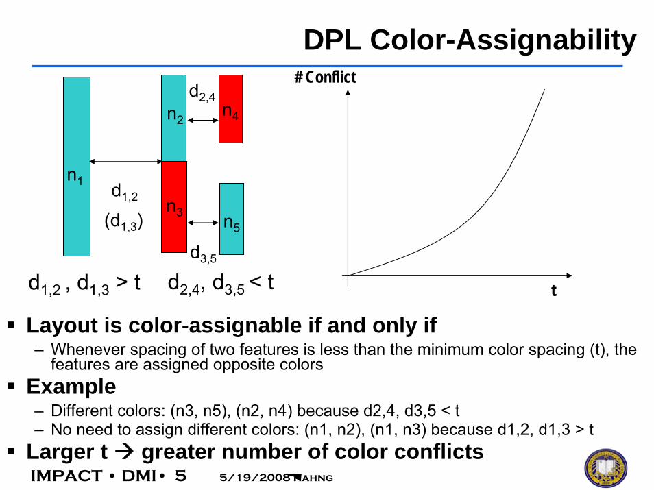
DPL Color-Assignability
d1,2
d1,2 , d1,3 > t d2,4, d3,5 < t
n1
n2n4
d2,4
n3 n5
d3,5
(d1,3)
t
# Conflict
Layout is color-assignable if and only if– Whenever spacing of two features is less than the minimum color spacing (t), the
features are assigned opposite colors Example– Different colors: (n3, n5), (n2, n4) because d2,4, d3,5 < t – No need to assign different colors: (n1, n2), (n1, n3) because d1,2, d1,3 > t
Larger t greater number of color conflicts

IMPACT • DMI• 6 5/19/2008 Kahng
M. Drapeau (SPIE 2007)
Conflict: Two features with < minimum color spacing have been assigned the same colorLike AltPSM phase conflict
Could solve by spacing (“decompaction”), but layout iteration is undesirable
Coloring Conflict

IMPACT • DMI• 7 5/19/2008 Kahng
Layout Decomposition and ColoringLayout Fracturing
Conflict Graph Construction
Conflict Cycle Detection
Node Splitting forConflict Cycle Removal
ILP based or heuristic Graph Coloring
Conflict Cycle?
Layout Partitioning
Yes
No
Find min-cost color assignment– Non-touching features with 0 < d(i,j) < t
different colors– Touching features assigned different colors
incur cost cij
IMPACT • DMI• 8 5/19/2008 Kahng
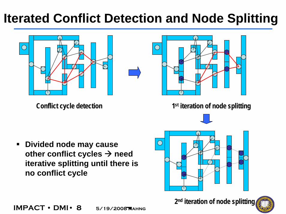
Iterated Conflict Detection and Node Splitting
Conflict cycle detection 1st iteration of node splitting
2nd iteration of node splitting
Divided node may cause other conflict cycles need iterative splitting until there is no conflict cycle
IMPACT • DMI• 9 5/19/2008 Kahng
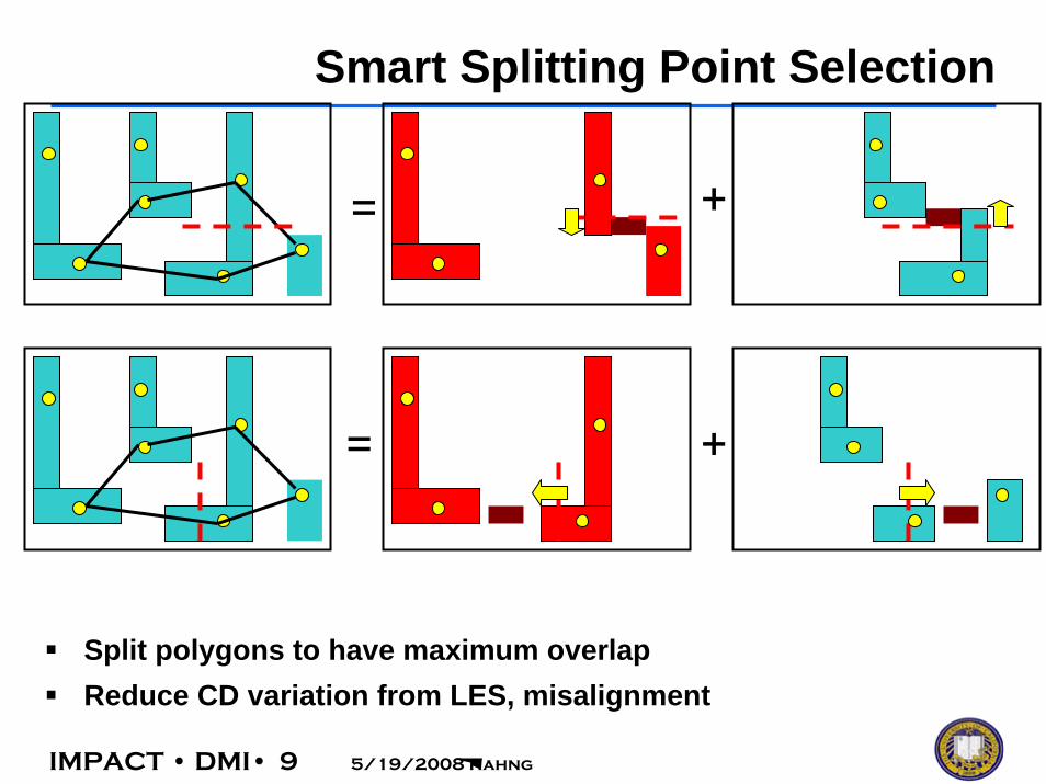
Smart Splitting Point Selection
Split polygons to have maximum overlapReduce CD variation from LES, misalignment
= +
= +

IMPACT • DMI• 10 5/19/2008 Kahng
Limits of Layout Decomposition
Require DPL-compliant design
o1o2
= +
Layout Decomposition Two Masks with Extended Overlap Design Change(Increase space)
Decomposition (1) Decomposition (2) Design Change(Increase space)
Design Change(Reduce size)
IMPACT • DMI• 11 5/19/2008 Kahng
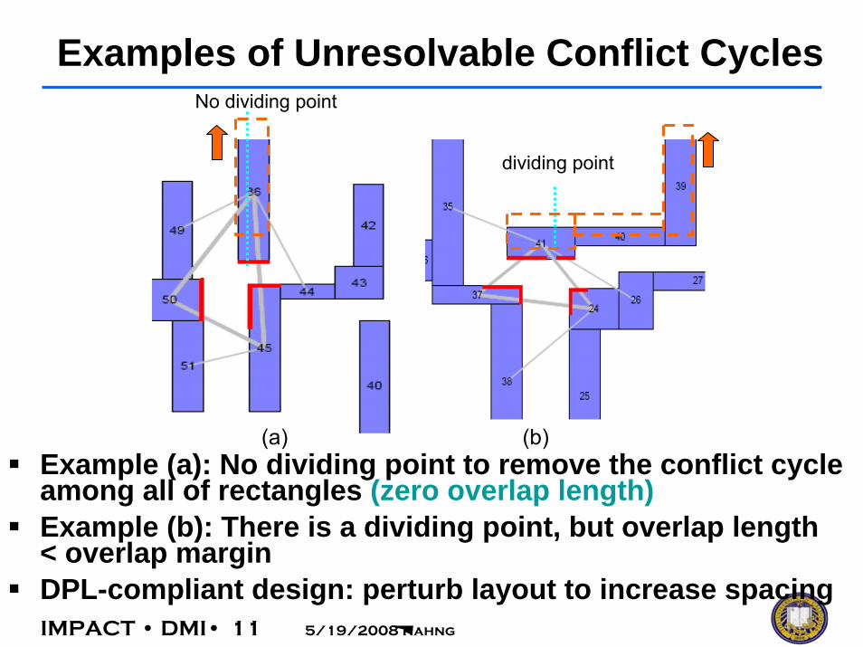
Examples of Unresolvable Conflict Cycles
Example (a): No dividing point to remove the conflict cycle among all of rectangles (zero overlap length)Example (b): There is a dividing point, but overlap length < overlap marginDPL-compliant design: perturb layout to increase spacing
(a) (b)
dividing point
No dividing point

IMPACT • DMI• 12 5/19/2008 Kahng
Min-Cost Color Assignment ProblemGiven:– A list of rectangles R which is color assignable, and maximum distance
between two features, t, at which the color assignment is constrainedFind:– A color assignment of rectangles to minimize the total cost
Subject to: – For any two adjacent non-touching features with 0 < d(i,j) < t, assign
different colors– For any two touching features (i.e., d(i; j) = 0), if they are assigned
different colors, there is a corresponding cost cij
– d(i,j): distance between features of ni and nj
– xi, xj: binary variables of features ni and nj
– t: minimum color spacing between features of ni and nj
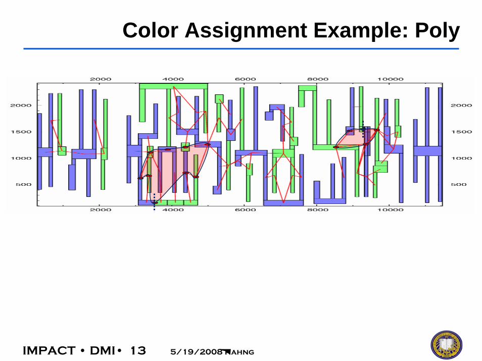
IMPACT • DMI• 13 5/19/2008 Kahng
Color Assignment Example: Poly

IMPACT • DMI• 14 5/19/2008 Kahng
Color Assignment Example: Metal

IMPACT • DMI• 15 5/19/2008 Kahng
Layout Decomposition SummaryColor-assignment– Successful color-assignment for design decomposition – Smart splitting point selection to maximize overlap length
(e.g., 8nm at 45nm) – ILP color assignment algorithm minimizes #cuts and design
rule violations– Layout partitioning to improve runtime
Ongoing works– Variability-aware DPL decomposition
– Hierarchical layout decomposition for DPL– Minimize difference between the pitch distributions of two masks– Minimize #distinct DPL solutions across all instances of a given
master cell– Local, global density balance between two masks
IMPACT • DMI• 16 5/19/2008 Kahng
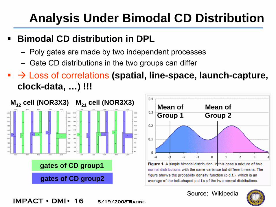
Analysis Under Bimodal CD DistributionBimodal CD distribution in DPL– Poly gates are made by two independent processes– Gate CD distributions in the two groups can differ
Loss of correlations (spatial, line-space, launch-capture, clock-data, …) !!!
Mean ofGroup 1
Mean ofGroup 2
Source: Wikipedia
gates of CD group1
M12 cell (NOR3X3) M21 cell (NOR3X3)
gates of CD group2

IMPACT • DMI• 17 5/19/2008 Kahng
Unimodal Modeling Is Too Pessimistic
Conventional unimodal representation (cf. Dusa et al. 2007) does not capture bimodal process variation
Key message: Our analysis and simulation studies (2008) suggest that DPL modeling, analysis, and yield optimization require close understanding of bimodal CD distribution
BC of G1
BC of G2 WC of G1WC of G2
G1G2

IMPACT • DMI• 18 5/19/2008 Kahng
MC Gate Delay, Leakage: Simulation Setup
SPICE model
– 65nm, Typical corner (TT), 1.0V, 25°C
SPICE circuit
– 65nm NVT: Nominal CD is “60nm”
CD variation model
– Assumption: small mean difference
– group1: N(meanM1=59nm, 3σ=5)
– group2: N(meanM2=61nm, 3σ=5)
Comparison:
– {Rise/Fall Delay, Leakage} of unimodal and bimodal distribution
605954 61
Bimodalgroup1
Bimodalgroup2
Worst CDBest CD
Unimodal
56 64 66
nmσnmMeannmσnm, Meannmσnm, Mean
uniuni
GG
GG
63 ,6053 6153 59
22
11
======
2n

IMPACT • DMI• 19 5/19/2008 Kahng
Simulation Results (MC iterations = 10,000)For bimodal distribution, two simulations are required.
– DPL1 : (2i-1)-th gate is group1 and 2i-th gate is group2– DPL2: 2i-th gate is group1 and (2i-1)-th gate is group2
Characteristics of DPL1 and DPL2 are different; unimodal too pessimistic
Delay (mean)
4.65E-11
4.70E-11
4.75E-11
4.80E-11
4.85E-11
4.90E-11
4.95E-11
5.00E-11
DPL1 DPL2 DPL1 DPL2
Bimodal Unimodal Bimodal Unimodal
Delay (sigma)
0
5E-13
1E-12
1.5E-12
2E-12
2.5E-12
DPL1 DPL2 DPL1 DPL2
Bimodal Unimodal Bimodal Unimodal
Leakage (mean)
0.00E+00
1.00E-08
2.00E-08
3.00E-08
4.00E-08
5.00E-08
DPL1 DPL2 DPL1 DPL2
Bimodal Unimodal Bimodal Unimodal
Leakage (sigma)
0.00E+00
5.00E-07
1.00E-06
1.50E-06
2.00E-06
DPL1 DPL2 DPL1 DPL2
Bimodal Unimodal Bimodal Unimodal
risefall
risefall
Input 1Input 0
Input 1Input 0
IMPACT • DMI• 20 5/19/2008 Kahng
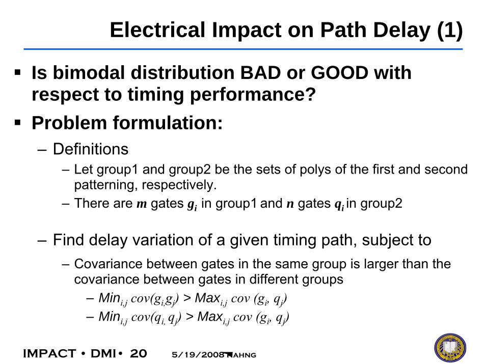
Electrical Impact on Path Delay (1)
Is bimodal distribution BAD or GOOD with respect to timing performance?Problem formulation:– Definitions
– Let group1 and group2 be the sets of polys of the first and second patterning, respectively.
– There are m gates gi in group1 and n gates qi in group2
– Find delay variation of a given timing path, subject to – Covariance between gates in the same group is larger than the
covariance between gates in different groups– Mini,j cov(gi,gj) > Maxi,j cov (gi, qj)– Mini,j cov(qi, qj) > Maxi,j cov (gi, qj)

IMPACT • DMI• 21 5/19/2008 Kahng
Electrical Impact on Path Delay (2)
By definition:σ2(x+y) = σ2(x)+ σ2(y) + 2 cov (x,y)
Delay variation of a timing path:
Path delay variation will be reducedHowever, reduced variation does not necessarily imply good behavior from the design and signoff perspective
( ) ( )
( ) ( ) ( )∑∑∑
∑∑
∑∑
+++
+=
⎟⎟⎠
⎞⎜⎜⎝
⎛+=
jiji
jiji
jiji
ii
ii
ji
ii
qdgdqdqdgdgd
qdgd
qdgdpathd
,,,
22
22
)(),(cov2)(),(cov2)(),(cov2
)()(
)()())((
σσ
σσ
( ) ( ) ( )on.distributi unimodalan smaller th ison distributi bimodal ofvariation
,)(),(covor )(),(covan smaller th is )(),(cov Since jijiji qdqdgdgdqdgd

IMPACT • DMI• 22 5/19/2008 Kahng
Simulation Setup for Corner Cases (1)Test cases– Exhaustive simulation on both min and max corners of each CD group
requires exponential number of simulations to the number of stages.
– Simple 4-stage delay chain: 2 (corners for CD group 1) x 2 (corners for CD group 2)
x 24 (combinations of CD groups 1, 2 for 4 gates) = 64 cases
SPICE model– 45nm PTM, Typical corner (TT), 1.0V, 25 °C
SPICE circuit– 45nm INVX4 and BUFX4 from Nangate Open Cell Library
N-stage
2-types 2-types 2-types 2-types
M1 M2WW Max MaxBB Min MinBW Min MaxWB Max Min
Process corners

IMPACT • DMI• 23 5/19/2008 Kahng
Simulation Setup for Corner Cases (2)CD variation model
– Realistic bimodal with mean difference
– Pooled unimodal: – CD model can account for
physical CD distribution of entire population
– CD variation increases with increasing mean difference.
Path sequences
M1 M2
Mean 3s Mean 3s
MeanDiff Uni-modal 50.00 2.00 - -
Pooled 50.00 2.00 - -
Bimodal 50.00 2.00 50.00 2.00
Pooled 50.00 2.50 - -
Bimodal 49.50 2.00 50.50 2.00
Pooled 50.00 3.61 - -
Bimodal 49.00 2.00 51.00 2.00
Pooled 50.00 4.92 - -
Bimodal 48.50 2.00 51.50 2.00
Pooled 50.00 6.32 - -
Bimodal 48.00 2.00 52.00 2.00
Pooled 50.00 7.76 - -
Bimodal 47.50 2.00 52.50 2.00
Pooled 50.00 9.22 - -
Bimodal 47.00 2.00 53.00 2.00 6nm
5nm
4nm
3nm
2nm
1nm
0nm
Inverter chain Buffer chainCase1 M1_M1_M1_M1 M12_M12_M12_M12Case2 M1_M1_M1_M2 M12_M12_M12_M21Case3 M1_M1_M2_M1 M12_M12_M21_M12Case4 M1_M1_M2_M2 M12_M12_M21_M21Case5 M1_M2_M1_M1 M12_M21_M12_M12Case6 M1_M2_M1_M2 M12_M21_M12_M21Case7 M1_M2_M2_M1 M12_M21_M21_M12Case8 M1_M2_M2_M2 M12_M21_M21_M21Case9 M2_M1_M1_M1 M21_M12_M12_M12
Case10 M2_M1_M1_M2 M21_M12_M12_M21Case11 M2_M1_M2_M1 M21_M12_M21_M12Case12 M2_M1_M2_M2 M21_M12_M21_M21Case13 M2_M2_M1_M1 M21_M21_M12_M12Case14 M2_M2_M1_M2 M21_M21_M12_M21Case15 M2_M2_M2_M1 M21_M21_M21_M12Case16 M2_M2_M2_M2 M21_M21_M21_M21
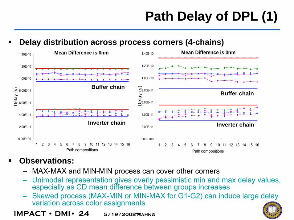
IMPACT • DMI• 24 5/19/2008 Kahng
0.00E+00
2.00E-11
4.00E-11
6.00E-11
8.00E-11
1.00E-10
1.20E-10
1.40E-10
1 2 3 4 5 6 7 8 9 10 11 12 13 14 15 16Path compositions
Del
ay (s
)
0.00E+00
2.00E-11
4.00E-11
6.00E-11
8.00E-11
1.00E-10
1.20E-10
1.40E-10
1 2 3 4 5 6 7 8 9 10 11 12 13 14 15 16Path compositions
Del
ay (s
)
Mean Difference is 0nm Mean Difference is 3nm
Inverter chain
Buffer chain
Inverter chain
Buffer chain
Delay distribution across process corners (4-chains)
Observations: – MAX-MAX and MIN-MIN process can cover other corners– Unimodal representation gives overly pessimistic min and max delay values,
especially as CD mean difference between groups increases– Skewed process (MAX-MIN or MIN-MAX for G1-G2) can induce large delay
variation across color assignments
Path Delay of DPL (1)

IMPACT • DMI• 25 5/19/2008 Kahng
Path Delay of DPL (2)Normalized delay variations ( Sigma / Mean )– Mean and sigma of a long inverter chain (16 stages) over all process
corners (Min and Max combinations)– Alternatively colored paths have smaller delay variation
this is a design optimization!
6.0
8.0
10.0
12.0
14.0
16.0
18.0
M1-M1-… M1-M2-… M2-M1-… M2-M2-…
Path composition
Sig
ma
/ Mea
n (%
)
0n 1n 2n3n 4n 5n6n

IMPACT • DMI• 26 5/19/2008 Kahng
Electrical Impact on Timing Slack
Timing slack
Timing slack variation
– I.e., uncorrelated clock and data path creates large slack variationClock skew– Especially, clock skew from uncorrelated launching and capturing clock
paths are a major source of timing slack variation.
pathdatacyclepathclockslack TTTT __ −+=
( )pathdatapathclockTTT TTpathdatapathclockslack __
222 ,cov2__
−+= σσσLarge correlation is better
for the timing slack

IMPACT • DMI• 27 5/19/2008 Kahng
Illustration of Timing Analysis
DPLPath delay variation is smallNo spatial correlation assumedExample circuit:– Clock path delay and data path
delay is same– Mean delay is 10ns
– Variation of the path delays:– ±2ns
– Worst slack calculation without spatial correlation
Single exposure casePath delay variation is largePerfect spatial correlation assumedExample circuit:
– Clock path delay and data path delay is same,
– Mean delay is 10ns
– Variation of the path delays:– ±5ns
– Worst slack calculation with perfect spatial correlation
Data(8~12ns)
Clock(8~12ns)
Data(5ns)
Clock(5ns)
Data(15ns)
Clock(15ns)
orWorst slack = 5-5=0ns
Worst slack = 15-15=0ns
Worst slack = min(clock) – max(data)= 8 – 12 = 4ns
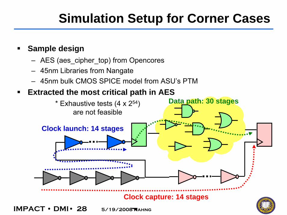
IMPACT • DMI• 28 5/19/2008 Kahng
Simulation Setup for Corner Cases
Sample design– AES (aes_cipher_top) from Opencores– 45nm Libraries from Nangate– 45nm bulk CMOS SPICE model from ASU’s PTM
Extracted the most critical path in AES
Clock launch: 14 stages
Clock capture: 14 stages
Data path: 30 stages* Exhaustive tests (4 x 254)are not feasible

IMPACT • DMI• 29 5/19/2008 Kahng
Clock Skew of DPL
Assumption: Data path coloring is fixedClock path configuration
Even for the zero mean difference case, clock skew exists and increases with mean difference– Pooled unimodal can not distinguish this clock skew
Implication for clock network design– Use the same colored cells for both clock paths– Alternatively colored path can further reduce variation
Case Launch Capture1 M12+M12…
M21+M21…M12+M12…M21+M21…M12+M21…
M12+M12…2 M21+M21…3 M21+M21…4 M12+M12…5 M12+M21…
0.00E+00
1.00E-11
2.00E-11
3.00E-11
4.00E-11
5.00E-11
6.00E-11
0nm 1nm 2nm 3nm 4nm 5nm 6nm
Mean difference (nm)
Clo
ck s
kew
(s)
Case1
Case2
Case3Case4Case5
Max: 53.4 ps@ 6nm difference
Max: 22.7 ps@ 0nm difference
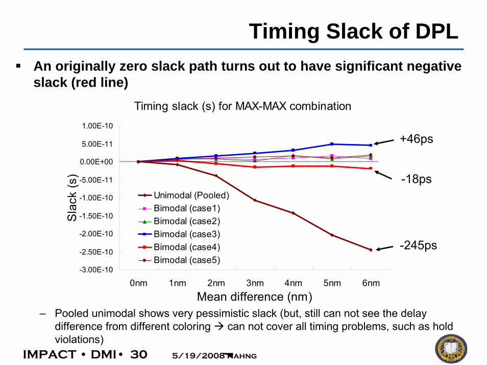
IMPACT • DMI• 30 5/19/2008 Kahng
Timing Slack of DPLAn originally zero slack path turns out to have significant negative slack (red line)
– Pooled unimodal shows very pessimistic slack (but, still can not see the delay difference from different coloring can not cover all timing problems, such as hold violations)
Timing slack (s) for MAX-MAX combination
-3.00E-10
-2.50E-10
-2.00E-10
-1.50E-10
-1.00E-10
-5.00E-11
0.00E+00
5.00E-11
1.00E-10
0nm 1nm 2nm 3nm 4nm 5nm 6nmMean difference (nm)
Sla
ck (s
)
Unimodal (Pooled)Bimodal (case1)Bimodal (case2)Bimodal (case3)Bimodal (case4)Bimodal (case5)
-18ps
+46ps
-245ps

IMPACT • DMI• 31 5/19/2008 Kahng
DPL Analysis Implications Summary
Observations– Bimodal CD distribution in DPL increases within-die
variation Increases design difficulty– Bimodal-aware timing analysis and optimization are
necessary
Research directions– Clock path design to reduce clock skew variation– Data path design to reduce worst-case delay and
delay variation– Flip-flop design to improve robustness over the
bimodal process corners

IMPACT • DMI• 32 5/19/2008 Kahng
Conclusion
Research performed by:– Kwangok Jeong– Chul-Hong Park– Dr. Hailong Yao
IMPACT member company feedback– When we start IMPACT research at UCSD, will DPL
enablement (e.g., as scoped here) be of interest?– What particular directions (cell layout, auto-placement,
timing model characterization, variability-minimizing optimizations, …) are of greatest interest?
– What collaboration and validation mechanisms?
IMPACT • DMI• 33 5/19/2008 Kahng
Thank You!