f26 32gb mlc nand flash memory tsop legacy - olimex · pdf filepreliminary h27ubg8t2btr-bc...
TRANSCRIPT

Preliminary
H27UBG8T2BTR-BC Series
32Gb(4096M x 8bit) Legacy MLC NAND Flash
Rev 0.7 / Jan. 2011 1
F26 32Gb MLC NAND Flash Memory
TSOP Legacy
H27UBG8T2BTR-BCH27UCG8U5BTR-BC
This document is a general product description and is subject to change without notice. Hynix does not assume any responsibilityfor use of circuits described. No patent licenses are implied.

Preliminary
H27UBG8T2BTR-BC Series
32Gb(4096M x 8bit) Legacy MLC NAND Flash
Rev 0.7 / Jan. 2011 2
Document Title
32Gbit(4096M x 8bit) Legacy NAND Flash Memory
Revision History
Revision No. History Draft Date Remark
0.0 Initial Draft Oct. 13. 2010 Preliminary
0.1 ~ 0.6 1st ~ 6th internal release Dec. 20. 2010 Preliminary
0.7 Correct Figure4.Array Organization(Page10) Jan. 03. 2011 Preliminary

Preliminary
H27UBG8T2BTR-BC Series
32Gb(4096M x 8bit) Legacy MLC NAND Flash
Rev 0.7 / Jan. 2011 3
■ Multi Level Cell(MLC) Technology
■ NAND Interface- x8 bus width- Multiplexed address/ Data-Pin-out compatibility for all densities
■ Power Supply Voltage- VCC = 2.7 V ~ 3.6 V- VCCQ = 2.7 V ~ 3.6 V / 1.7 V ~ 1.95 V
■ Organization- Page size : (8K+640spare)bytes- Block size : (2048K+160K)bytes- Plane size : 1024blocks- Device size : 2048blocks
■ Page Read/Program Time- Random Read Time(tR): 90us(MLC), 40us(SLC)- Sequential Access: 20 ns (min.)- Page Program Time: 1300us(MLC), 500us(SLC)- Parallel operations on both planes available,effectively halving program, read and erase time
■ Block Erase-Block Erase Time: 3.5ms(Typ.)
■ Multi-Plane Architecture- Two independent planes architecture- Parallel operations on both planes available, effectively halving program, read and erase time
■ Command Set- ONFI 2.2 Compliant Command Set- Interleaved Copyback Program - Read Unique IDs
■ Package- Package type : TSOP- Chip count : SDP(1CE, Single) = 1stack
DDP(2CE, Dual) = 2stack- Pin Count : 48- Size : 12mm x 20mm x 1.2mm
■ Electronic Signature- 1st cycle: Manufacturer Code- 2nd cycle: Device Code- 3rd cycle: Internal chip number, Cell Type, Number of
Simultaneously Programmed Pages.- 4th cycle: Page size, Block size, Organization,
Spare size- 5th cycle: Multi-plane information- 6th cycle: Technology, EDO, Interface
■ Chip Enable Don’t Care- Simple interface with microcontroller
■ Hardware Data Protection- Program/Erase locked during Power transitions
■ Reliability- TBD
Product Feature

Preliminary
H27UBG8T2BTR-BC Series
32Gb(4096M x 8bit) Legacy MLC NAND Flash
Rev 0.7 / Jan. 2011 4
1. SUMMARY DESCRIPTION………………………………………………………………………………………..
1.1. Product List…………………………………………………………………………..………………………….….1.2. Pin Descriptions……………………………………………………………………..…………………..…….....1.3. Pin Diagram................................................................................................................................1.4. Pin Assignments………………………………………………………………………..…………………..……..1.5. Block Diagram.............................................................................................................................1.6. Array Organization......................................................................................................................1.7. Addressing..................................................................................................................................
1.7.1. Addressing (MLC mode) …………………………………………………………………………………..1.7.2. Addressing (SLC mode) ……………………………………………………………………………………
1.8. Command Set……………………………………………………………………………….………………………1.9. Mode Selection…………………………………………………………………………….……………………….1.10. Bad Block Management ………………………………………………………………….…………………….1.11. Bad Block Replacement…………………………………………………………………….…………………..
2. Electrical Characteristics……………………………………………………………………...…………………
2.1. Valid Blocks…………………………………………………………………………………………….……………2.2. Absolute Maximum Rating………………………………………………………………………….…………..2.3. DC and Operating Characteristics ……………………………………………………………….……………2.4. AC Test Conditions…………………………………………………………………………………….…………..2.5. Pin Capacitance (TA=25℃, F=1.0㎒) ..........................................................................................2.6. Program/ Read / Erase Characteristics .....................................................................................2.7. AC Timing Characteristics………………………………………………………………………….……………2.8. Status Register Coding……………………………………………………………………………………….….
2.8.1. Status Register Coding For 70h/78h command ………….…………………………………….…..2.8.2. Status Register Coding For 75h command……………………….……………………………….….
2.9. Device Identifier Coding…………………………………………………………………………………….…..2.10. Read ID Data Table………………………………………………………………………………………….….
2.10.1. 3rd Byte of Device Identifier Description…………………………………………………………….2.10.2. 4th Byte of Device Identifier Description…………………………………………………………....2.10.3. 5th Byte of Device Identifier Description…………………………………………………………….2.10.4. 6th Byte of Device Identifier Description…………………………………………………………….
3. Timing Diagram………………………………………………………………………………………….………..…
3.1. Command Latch Cycle Timings……………………………………………………………………….………..3.2. Address Latch Cycle Timings.………………………………………………………………………….……….3.3. Input Data Latch Cycle Timings…………………………………………………………………….………….3.4. Data Output Cycle Timings …………………………………………………………………………….……….3.5. Data Output Cycle Timings (EDO type)……………………………………………………………….……….3.6. Read Status Cycle Timings…………………………………………………………………………….………..3.7. Multi Plane Read Status Timings…………………………………………………………………….………..3.8. Page Read Operation Timings.……………………………………………………………………….………..3.9. Page Read Operation Timings (Intercepted by CE#)………………………………………………….…….3.10. Page Read Operation Timings with CE# don’t care…………………………………………….……….3.11. Random Data Output Timings………………………………………………………………………….…….3.12. Multi Plane Page Read Operation with Random Data output Timings……………………….…….3.13. Cache Read Operation Timings……………………………………………………………………….………3.14. Multi Plane Cache Read Operation Timings……………………………………………………….………3.15. Read ID Operation Timings……………………………………………………………………………….…..3.16. Page Program Operation Timings……………………………………………………………………….…..3.17. Page Program Operation Timings with CE# don’t care………………………………………………..
667891010111111121314151616161717181819202021212222222323242424252526262727282829293031323233
Table of Contents

Preliminary
H27UBG8T2BTR-BC Series
32Gb(4096M x 8bit) Legacy MLC NAND Flash
Rev 0.7 / Jan. 2011 5
3.18. Random Data Input Timings…………………………………………………………………………………3.19. Multi Plane Page Program Operation Timings…………………………………………………………..3.20. Copy-Back Program Operation Timings with Random Date Input.………………………………..3.21. Cache Program Operation Timings…………………………………………………………………………3.22. Multi Plane Cache Program Operation Timings………………………………………………………….3.23. Block Erase Operation Timings………………………………………………………………………………3.24. Multi Plane Erase Operation Timings......................................................................................3.25. Reset Timings……………………………………………………………………………………………………
4. DEVICE OPERATION………………………………………………………………………………………………
4.1. Page Read…………………………………………………………………………………………………………..4.2. Cache Read…………………………………………………………………………………………………………4.3. Cache Read Enhanced …………………………………………………………………………………………..4.4. Multi Plane Page Read…………………………………………………………………………………………..4.5. Multi Plane Cache Read ………………………………………………………………………………………..4.6. Multi Plane Cache Read Enhanced …………………………………………………………………………..4.7. Read ID……………………………………………………………………………………………………………..4.8. Read Status Register…………………………………………………………………………………………….4.9. Page Program……………………………………………………………………………………………………..4.10. Multi Plane Program……………………………………………………………………………………………4.11. Cache Program.………………………………………………………………………………………………….4.12. Multi Plane Cache Program.………………………………………………………………………………….4.13. Copy-Back Program…………………………………………………………………………………………….4.14. Multi-Plane Copy-Back Program…………………………………………………………………………….4.15. Block Erase………………………………………………………………………………………………………..4.16. Multi Plane Block Erase………………………………………………………………………………………..4.17. Reset……………………………………………………………………………………………………………….
5. OTHER FEATURES…………………………………………………………………………………………………..
5.1. Data Protection & Power on/off Sequence…………………………………………………………………5.2. Ready / Busy.………………………………………………………………………………………………………5.3. Write Protect Operation…………………………………………………………………………………………
6. Application Notes and Comments…………………………………………………………………………….
6.1. Paired Page Address Information.……………………………………………………………………………6.2. Acceptable Command after 80h………………………………………………………………………………6.3. Acceptable Command between Start command and Confirm command…………………………...6.4. Restriction of Read Status Value in Multi Plane Operation…………………………………………….6.5. Page Program Failure……………………………………………………………………………………………6.6. Restriction Multi Plane Operation.……………………………………………………………………………
33343535363637373838393940414142434445464849505152525353545556565757575757

Preliminary
H27UBG8T2BTR-BC Series
32Gb(4096M x 8bit) Legacy MLC NAND Flash
Rev 0.7 / Jan. 2011 6
Table 1 : List of supported versions / packages
PART NUMBER ORGANIZATION OPERATING RANGE PACKAGE
H27UBG8T2BTR-BC X8 2.7 to 3.6V TSOP-48/SDP
H27UCG8U5BTR-BC X8 2.7 to 3.6V TSOP-48/DDP
1. Summary Description
The product part NO. H27UBG8T2BTR-BC is a single 3.3V 32Gbit NAND flash memory. The Device contains 2 planes in a single die. Each plane is made up of the 1,024 blocks. Each block consists of 256 programmable pages. Each page contains 8,832bytes. The pages are subdivided into an 8,192byte main data storage area with a spare 640byte district.
Page program operation can be performed in typical 1300us, and a single block can be erased in typical 3.5ms.
1.1. Product List

Preliminary
H27UBG8T2BTR-BC Series
32Gb(4096M x 8bit) Legacy MLC NAND Flash
Rev 0.7 / Jan. 2011 7
Pin Name Description
I/O 0―I/O 7
DATA INPUTS/OUTPUTSThe I/O pins is used to COMMAND LATCH cycle, ADDRESS INPUT cycle, and DATA in-outcycles during read / write operations. The I/O pins float to High-Z when the device isdeselected or the outputs are disabled.
CLECOMMAND LATCH ENABLEThis input activates the latching of the I/O inputs inside the Command Register on the Risingedge of Write Enable (WE#).
ALEADDRESS LATCH ENABLEThis input activates the latching of the I/O inputs inside the Address Register on the Risingedge of Write Enable (WE#).
CE#
CHIP ENABLEThis input controls the selection of the device. When the device is busy, CE# low does notdeselect the memory. The device goes into Stand-by mode when CE# goes High during thedevice is in Ready state. The CE# signal is ignored when device is in Busy state, and will notenter Standby mode even if the CE# goes high.
WE#WRITE ENABLEThis input acts as clock to latch Command, Address and Data. The I/O inputs are latched onthe rise edge of WE#.
RE#
READ ENABLEThe RE# input is the serial data-out control, and when active drives the data onto the I/O bus. Data is valid tREA after the falling edge of RE# which also increments the internal column address counter by one.
WP#
WRITE PROTECTThe WP# pin, when Low, provides a hardware protection against undesired write operations.Hardware Write Protection is activated when the Write Protect pin is low. In this conditionmodify operation do not start and the content of the memory is not altered. Write Protect pinis not latched by Write Enable to ensure the protection even during the power up phases.
R/B#READY / BUSYThe Ready/Busy output is an Open Drain pin that signals the state of the memory.
VCCQ SUPPLY VOLTAGE FOR I/O BUFFER
VSSQ GROUND FOR I/O BUFFER
VCC
SUPPLY VOLTAGEThe VCC supplies the power for all the operations. (Read, Write, and Erase).
VSS GROUND
NC NO CONNECTED
NOTE: A 0.1uF capacitor should be connected between the Vcc Supply Voltage pin and the Vss Ground pin to decouple the current surges from the power supply. The PCB track widths must be sufficient to carry the currents required during program and erase operations.
Table 2 : Signal descriptions
1.2. Pin Descriptions

Preliminary
H27UBG8T2BTR-BC Series
32Gb(4096M x 8bit) Legacy MLC NAND Flash
Rev 0.7 / Jan. 2011 8
Figure 1 : Pin diagram(SDP)
VCC
ALE
CLE
VSS
R/B#
IO0~IO7CE#
WE#
RE#
WP#
VSSQ
VCCQ
1.3. Pin Diagram
Preliminary
H27UBG8T2BTR-BC Series
32Gb(4096M x 8bit) Legacy MLC NAND Flash
Rev 0.7 / Jan. 2011 9
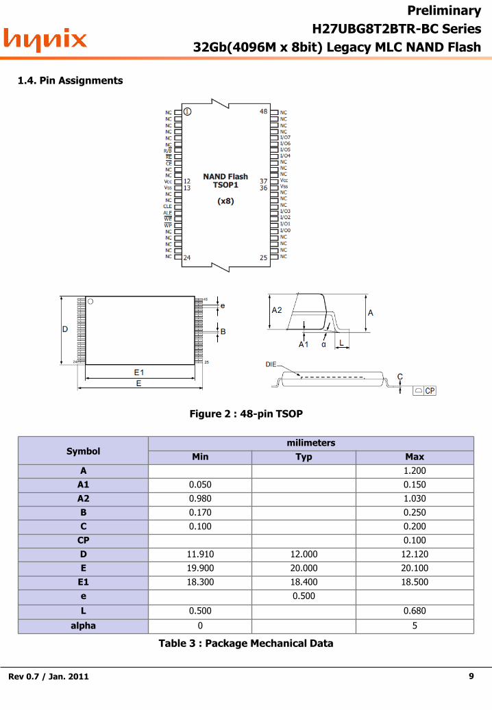
Symbolmilimeters
Min Typ Max
A 1.200
A1 0.050 0.150
A2 0.980 1.030
B 0.170 0.250
C 0.100 0.200
CP 0.100
D 11.910 12.000 12.120
E 19.900 20.000 20.100
E1 18.300 18.400 18.500
e 0.500
L 0.500 0.680
alpha 0 5
Figure 2 : 48-pin TSOP
Table 3 : Package Mechanical Data
1.4. Pin Assignments

Preliminary
H27UBG8T2BTR-BC Series
32Gb(4096M x 8bit) Legacy MLC NAND Flash
Rev 0.7 / Jan. 2011 10
Figure 3 : Block diagram(SDP)
Figure 4 : Array organization
1.5. Block Diagram
1.6. Array Organization

Preliminary
H27UBG8T2BTR-BC Series
32Gb(4096M x 8bit) Legacy MLC NAND Flash
Rev 0.7 / Jan. 2011 11
Bus cycle I/O0 I/O1 I/O2 I/O3 I/O4 I/O5 I/O6 I/O7
1st Cycle A0 A1 A2 A3 A4 A5 A6 A7
2nd Cycle A8 A9 A10 A11 A12 A13 L(1) L(1)
3rd Cycle A14 A15 A16 A17 A18 A19 A20 A21
4th Cycle A22 A23 A24 A25 A26 A27 A28 A29
5th Cycle A30 A31 A32 L(1) L(1) L(1) L(1) L(1)
Notes: 1. L must be set to Low. 2. The device ignores any additional address input cycle than required. 3. The Address consists of column address (A0~A13), page address (A14 ~ A21), plane address (A22),
and block address (A23 ~ the last address).
Bus cycle I/O0 I/O1 I/O2 I/O3 I/O4 I/O5 I/O6 I/O7
1st Cycle A0 A1 A2 A3 A4 A5 A6 A7
2nd Cycle A8 A9 A10 A11 A12 A13 L(1) L(1)
3rd Cycle A14 A15 A16 A17 A18 A19 A20 A21
4th Cycle A22 A23 A24 A25 A26 A27 A28 A29
5th Cycle A30 A31 L(1) L(1) L(1) L(1) L(1) L(1)
Notes: 1. L must be set to Low. 2. The device ignores any additional address input cycle than required. 3. The Address consists of column address (A0~A13), page address (A14 ~ A20), plane address (A21),
and block address (A22 ~ the last address).
1.7. Addressing
1.7.1. Addressing(MLC mode)
1.7.2. Addressing(SLC mode)

Preliminary
H27UBG8T2BTR-BC Series
32Gb(4096M x 8bit) Legacy MLC NAND Flash
Rev 0.7 / Jan. 2011 12
FUNCTION1st
Cycle
Number of
Addresscycles
DataInput cycles
2nd
Cycle
Numberof
Addresscycles
Datainput cycles
3rd
Cycle
Acceptable command
Duringbusy
PAGE READ 00h 5 - 30h - - - No
READ FOR COPY-BACK 00h 5 - 35h - - - No
RANDOM DATA OUTPUT1) 05h 2 - E0h - - - No
SINGLE/MULTI-PLANECACHE READ 5) 31h - - - - - - No
SINGLE/MULTI-PLANECACHE READ END 5) 3Fh - - - - - - No
READ ID 90h 1 - - - - - No
READ STATUS REGISTER 70h - - - - - - Yes
PAGE PGM (start)/CACHE PGM 5) (end)
80h 5 Yes 10h - - - No
RANDOM DATA INPUT1) 85h 2 Yes - - - - No
COPY-BACK PGM 85h 5 option 10h - - - No
CACHE PGM (start)5) 80h 5 Yes 15h - - - No
BLOCK ERASE 60h 3 - D0h - - - No
RESET FFh - - - - - - Yes
MULTI-PLANE PAGE READ 60h 3 - 60h 3 - 30h No
MULTI-PLANE CACHE READSTART 5) 6) 60h 3 - 60h 3 - 33h No
MULTI-PLANE READ FORCOPY-BACK
60h 3 - 60h 3 - 35h No
MULTI-PLANE BLOCK ERASE 60h 3 - 60h 3 - D0h No
MULTI-PLANE RANDOMDATA OUTPUT 1) 3) 00h 5 - 05h 2 - E0h No
MULTI-PLANE READSTATUS REGISTER
78h 3 - - - - - Yes
MULTI-PLANE READSTATUS REGISTER (legacy)
75h - - - - - - Yes
MULTI-PLANE PAGE PGM/MULTI-PLANE CACHE PGM(end)
80h 5 Yes 11h-81h 2) 5 Yes 10h No
MULTI-PLANE COPY-BACKPGM
85h 5 option 11h-81h 2) 5 option 10h No
MULTI-PLANE CACHE PGM(start) 5) 80h 5 Yes 11h-81h 2) 5 Yes 15h No
CACHE READ ENHANCED 00h 5 - 31h - - - No
MULTI-PLANE CACHE READENHANCED
60h 3 - 60h 3 - 31h No
1.8. Command Set

Preliminary
H27UBG8T2BTR-BC Series
32Gb(4096M x 8bit) Legacy MLC NAND Flash
Rev 0.7 / Jan. 2011 13
Notes: 1. Random Data Input/Output must be performed in a selected page.2. Any command between 11h and 81h is prohibited except 70h, 78h, 75h and FFh. 3. Multi-plane Random data-out must be used after multi plane read operations
(Multi Plane Page Read, Multi Plane Cache Read and Multi Plane Read for Copy Back). 4. Do not change plane address order when using all MULTI-PLANE operations.5. All cache operation (cache program, cache read) is available only within a block.6. It‟s possible to confirm the multi-plane cache read first step using both 30h and 33h.
Caution: 1. Any undefined command inputs are prohibited except for above command set. 2. Multi plane page read, multi plane cache read, and multi plane read for copy-back must be used
after Multi plane programmed page, multi plane cache program, and multi plane copy-back program.
CLE ALE CE# WE# RE# WP# MODE
H L L H XRead Mode
Command Input
L H L H X Address Input ( 5 Cycles )
H L L H HWrite Mode
Command Input
L H L H H Address Input ( 5 Cycles )
L L L H H Data Input
L L L H X Sequential Read and Data Output
X X X H H X During Read (Busy)
X X X X X H During Program (Busy)
X X X X X H During Erase (Busy)
X X X X X L Write Protect
X X H X X 0V/Vcc Stand-By
Notes:1. X can be VIL or VIH. H = Logic level HIGH. L = Logic level LOW.2. WP# should be biased to CMOS high or CMOS low for stand-by mode.3. WE# and RE# during Read Busy must be keep on high to prevent unplanned
command/address/data input or to avert unintended data out. In this time, only Reset, Read Status, and Multi Plane Read Status can be inputted to the device.
1)
1)
1)
3) 3)
2)
1.9. Mode Selection

Preliminary
H27UBG8T2BTR-BC Series
32Gb(4096M x 8bit) Legacy MLC NAND Flash
Rev 0.7 / Jan. 2011 14
Figure 5 : Bad block management flow chart
Notes:1. Do not try to erase the detected bad blocks, because the bad bock information will be lost.2. Do not perform program and erase operation in invalid block, it is impossible to guarantee the
Input data and to ensure that the function is normal.
1.10. Bad Block Management
Devices with Bad Blocks have the same quality level and the same AC and DC characteristics as devices where all the blocks are valid. A Bad Block does not affect the performance of valid blocks because it is isolated from the bit line and common source line by a select transistor. The devices are supplied with all the locations inside valid blocks erased (FFh). The Bad Block Information is written prior to shipping. Any block where the 1st Byte in the spare area of the First and Last page does not contain FFh is a Bad Block. The Bad Block Information must be read before any erase is attempted as the Bad Block Information may be erased. For the system to be able to recognize the Bad Blocks based on the original information it is recommended to create a Bad Block table following the flowchart shown in Figure 5. The 1st block, which is placed on 00h block address, is guaranteed to be a valid block at the time of shipment.

Preliminary
H27UBG8T2BTR-BC Series
32Gb(4096M x 8bit) Legacy MLC NAND Flash
Rev 0.7 / Jan. 2011 15
Table 4 : Block failure
Figure 6 : Block replacement
Notes:1. An error occurs on nth page of the Block A during Program or Erase operation.2. Data in Block A is copied to same location in Block B which is valid block.3. Nth page of block A which is in controller buffer memory is copied into nth page of Block B4. Bad block table should be updated to prevent from erasing or programming Block A.
1.11. Bad Block Replacement
This device may have the invalid blocks when shipped from factory. An invalid block is one that contains one or more bad bits. Over the lifetime of the device additional Bad Blocks may develop. In this case, the block has to be replaced by copying the data to a valid block. These additional Bad Blocks can be identified as attempts to program or erase them will give errors in the Status Register.The failure of a page program operation does not affect the data in other pages in the same block. Bad block can be replaced by re-programming the current data and copying the rest of the replaced block to an available valid block. Refer to Table 4 and Figure 6 for the recommended procedure to follow if an error occurs during an operation.
Operation Recommanded Procedure
Erase Block Replacement
Program Block Replacement
Read ECC

Preliminary
H27UBG8T2BTR-BC Series
32Gb(4096M x 8bit) Legacy MLC NAND Flash
Rev 0.7 / Jan. 2011 16
Symbol Min Typ Max Unit
Valid Block Number NVB 2000 2048 Blocks
Notes:1. The 1st block is guaranteed to be a valid block at the time of shipment.2. This single device has a maximum of 48 invalid blocks.3. Invalid blocks are one that contains one or more bad bits. The device may contain bad blocks
upon shipment.
Symbol ParameterValue
UnitMin
TA
Ambient Operating Temperature(Commercial Temperature Range)
0 to 70 ℃
Ambient Operating Temperature(Extended Temperature Range)
-25 to 85 ℃
Ambient Operating Temperature(Industrial Temperature Range)
-40 to 85 ℃
TBIAS Temperature Under Bias -50 to 125 ℃
TSTG Storage Temperature -65 to 150 ℃
VIO Input or Output Voltage -0.6 to 4.6 V
VCC Supply Voltage -0.6 to 4.6 V
Notes:1. Except for the rating “Operating Temperature Range”, stresses above those listed in the Table
“Absolute Maximum Ratings” may cause permanent damage to the device. These are stress ratings only and operation of the device at these or any other conditions above those indicated in theOperating sections of this specification is not implied. Exposure to Absolute Maximum Rating conditions for extended periods may affect device reliability.Refer also to the Hynix SURE Program and other relevant quality documents.
2. Minimum Voltage may undershoot to -2V during transition and for less than 20ns during transitions.
2. Electrical Characteristics
2.1. Valid Blocks
2.2. Absolute Maximum Rating

Preliminary
H27UBG8T2BTR-BC Series
32Gb(4096M x 8bit) Legacy MLC NAND Flash
Rev 0.7 / Jan. 2011 17
Parameter SymbolTest
Conditions
3.3VUnits
Min Typ Max
Power on reset current ICC0
FFh command input after power on
- -50 per device
mA
OperatingCurrent
Read ICC1
tRC= tRC(min),CE#=VIL, IOUT=0 ㎃
- - 50 mA
Program ICC2 - - 50 mA
Erase ICC3 - - 50 mA
Stand-by Current(TTL)
ICC4
CE#=VIH, WP#=0V/VCC
-- 1 mA
Stand-by Current (CMOS)
ICC5
CE#=VCC-0.2, WP#=0V/VCC -
10 50 uA
Input Leakage Current VIN=0 to VCC(MAX)
-- ±10 uA
Output Leakage Current ILO VOUT=0 to VCC(MAX)
-- ±10 uA
Input High Voltage VIH - Vccx0.8 - Vcc+0.3 V
Input Low Voltage VIL - -0.3 - 0.2xVcc V
Output High Voltage Level VOH IOH=-400 ㎂ 2.4 - - V
Output Low Voltage Level VOL IOL=2.1 ㎃ - - 0.4 V
Output Low Current (R/B#) IOL (R/B#) VOL=0.4V 8 10 - mA
ParameterValue
2.7V ≤ VccQ ≤ 3.6V
Input Pulse Levels 0 V to VCC
Input Rise and Fall Times 5 ㎱
Input and Output Timing Levels VCC / 2
Output Load (2.7V-3.6V) 1 TTL GATE and CL=50㎊
Note: These parameters are verified device characterization and are not 100% tested.
2.3. DC and Operating Characteristics
2.4. AC Test Conditions

Preliminary
H27UBG8T2BTR-BC Series
32Gb(4096M x 8bit) Legacy MLC NAND Flash
Rev 0.7 / Jan. 2011 18
Symbol Parameter Test Condition Min Max Unit
CIN Input Capacitance VIN = 0V - 10 pF
CI/O Input/Output Capacitance VIL = 0V - 10 pF
Parameter Symbol Min Typ Max Unit
Program (following 10h) tPROG - 1300 3500 us
Cache Program (following 15h) tCBSYW - 3500 us
Multi-Plane Program / Multi-Plane Cache Program /Multi-Plane Copy-Back Program (following 11h)
tDBSY - 3 5 us
Cache Read / Multi-Plane Cache Read(following 31h/3Fh)
tCBSYR 3 200 us
Block Erase / Multi-Plane Block Erase tBERS - 3.5 10 ms
Number of partial Program Cyclesin the same page
NOP - - 1 cycles
Notes:Typical value is measured at VCC=3.3V, TA=25℃. Not 100% tested.
2.5. Pin Capacitance (TA=25℃, F=1.0㎒)
2.6. Program/ Read / Erase Characteristics

Preliminary
H27UBG8T2BTR-BC Series
32Gb(4096M x 8bit) Legacy MLC NAND Flash
Rev 0.7 / Jan. 2011 19
Parameter Symbol3.3V
UnitMin Max
CLE setup time tCLS 10 ns
CLE Hold time tCLH 5 ns
CE# setup time tCS 20 ns
CE# hold time tCH 5 ns
WE# pulse width tWP 8 ns
ALE setup time tALS 10 ns
ALE hold time tALH 5 ns
Data setup time tDS 10 ns
Data hold time tDH 5 ns
Write cycle time tWC 20 ns
WE# high hold time tWH 10 ns
Data transfer from cell to register tR 90 us
ALE to RE# delay tAR 10 ns
CLE to RE# delay tCLR 10 ns
Ready to RE# low tRR 20 ns
RE# pulse width tRP 10 ns
WE# high to busy tWB 100 ns
Read cycle time tRC 20 ns
RE# access time tREA 16 ns
RE# high to output high Z tRHZ 100 ns
CE# high to output high Z tCHZ 50 ns
RE# high to output hold tRHOH 15 ns
RE# low to output hold tRLOH 5 ns
RE# or CE# high to output hold tCOH 15 ns
RE# high hold time tREH 8 ns
WE# high to RE# low tWHR 80 ns
WE# high to RE# low for Random data out tWHR2 200 ns
RE# high to WE# low tRHW 100 ns
Output high Z to RE# low tIR 0 ns
CE# low to RE# low tCR 10 ns
Address to data loading time tADL 200 ns
Device resetting time (Read/Program/Erase) tRST 20/30/500 us
Write protection time tWW 100 ns
2.7. AC Timing Characteristics

Preliminary
H27UBG8T2BTR-BC Series
32Gb(4096M x 8bit) Legacy MLC NAND Flash
Rev 0.7 / Jan. 2011 20
Notes:1. If Reset Command (FFh) is written at Ready state, the device goes into Busy for maximum 5us.2. Program / Erase Enable Operation: WP# high to WE# High.
Program / Erase Disable Operation: WP# Low to WE# High.3. The transition of the corresponding control pins must occur only while WE# is held low. 4. tADL is the time from the WE# rising edge of final address cycle to the WE# rising edge of first
data cycle.
I/OPage
ProgramBlock Erase
ReadCache Read
Cache Program
Coding
70h / 78h
0 Pass / Fail Pass / Fail N/A N/APass / Fail (N)
N page Pass : „0‟ Fail : „1‟
1 N/A N/A N/A N/APass /
Fail (N-1)N -1 page
Pass : „0‟ Fail : „1‟
2 N/A N/A N/A N/A N/A „0‟
3 N/A N/A N/A N/A N/A „0‟
4 N/A N/A N/A N/A N/A „0‟
5 N/A N/A N/AReady /
BusyReady /
BusyReady / Busy
Busy : „0‟ Ready : „1‟
6Ready /
BusyReady /
BusyReady /
BusyReady /
BusyReady /
BusyData Cache Ready / Busy
Busy : „0‟ Ready : „1‟
7Write
ProtectWriteProtect
Write Protect
Write Protect
Write Protect
Protected : „0‟Not Protected : „1‟
Notes: 1. I/O0: This bit is only valid for Program and Erase operations. During Cache Program operations, this
bit is only valid when I/O5 is set to one. 2. I/O1: This bit is only valid for cache program operations. This bit is not valid until after the second
15h command or the 10h command has been transferred in a Cache program sequence. When Cache program is not supported, this bit is not used.
3. I/O5: If set to one, then there is no array operation in progress. If cleared to zero, then there is acommand being processed (I/O6 is cleared to zero) or an array operation in progress. When overlapped interleaved operations or cache commands are not supported, this bit is not used.
4. I/O6: If set to one, then the device or interleaved address is ready for another command and allother bits in the status value are valid. If cleared to zero, then the last command issued is notyet complete and Status Register bits<5:0> are invalid value. When cache operations are in use, then this bit indicates whether another command can be accepted, and I/O5 indicateswhether the last operation is complete.
2.8. Status Register Coding
2.8.1. Status Register Coding For 70h/78h command

Preliminary
H27UBG8T2BTR-BC Series
32Gb(4096M x 8bit) Legacy MLC NAND Flash
Rev 0.7 / Jan. 2011 21
I/OPage
ProgramBlock Erase
ReadCache Read
Cache Program
Coding
75h
0 / Fail / Fail N/A N/AChip
Pass / Fail (N)
N page Pass : „0‟ Fail : „1‟
1Plane 0
Pass / FailPlane 0
Pass / FailN/A N/A
Plane 0Pass /
Fail (N)
N page Pass : „0‟ Fail : „1‟
2Plane 1
Pass / FailPlane 1
Pass / FailN/A N/A
Plane 1 Pass / Fail (N)
N page Pass : „0‟ Fail : „1‟
3 N/A N/A N/A N/APlane 0 Pass /
Fail (N-1)
N -1 page Pass : „0‟ Fail : „1‟
4 N/A N/A N/A N/APlane 1 Pass /
Fail (N-1)
N -1 page Pass : „0‟ Fail : „1‟
5 N/A N/A N/AReady /
BusyReady /
BusyReady / Busy
Busy : „0‟ Ready : „1‟
6Ready /
BusyReady /
BusyReady /
BusyReady /
BusyReady /
Busy
Data Cache Ready / Busy
Busy : „0‟ Ready : „1‟
7Write
ProtectWrite
ProtectWrite
ProtectWriteProtect
WriteProtect
Protected : „0‟Not Protected : „1‟
Parameter Symbol
Device Identifier Byte Description
1st Manufacturer Code
2nd Device Identifier
3rd Internal chip number, cell Type, Number of Simultaneously Programmed Pages, Interleaved Program, Write Cache.
4th Page size, Block size, Redundant area size
5th Plane Number, ECC Level
6th Technology (Design Rule), , Interface
2.8.2. Status Register Coding For 75h command
2.9. Device Identifier Coding

Preliminary
H27UBG8T2BTR-BC Series
32Gb(4096M x 8bit) Legacy MLC NAND Flash
Rev 0.7 / Jan. 2011 22
Part NumberVoltage (Vcc)
Voltage (Vccq)
BusWidth
ManufactureCode
Device Code
3rd 4th 5th 6th
H27UBG8T2BTR-BC 3.3V 3.3V X8 ADh D7h 94h DAh 74h C3h
3rd cycle Description I/O7 I/O6 I/O5 I/O4 I/O3 I/O2 I/O1 I/O0
Internal Chip Number
1248
0011
0101
Cell Type
2 Level Cell 4 Level Cell8 Level Cell16 Level Cell
0011
0101
Number of Simultaneously Programmed Pages
1248
0011
0101
Interleaved Program Between Multiple die
Not Supported
01
Write CacheNot
Supported01
2.10. Read ID Data Table
2.10.1. 3rd Byte of Device Identifier Description
2.10.2. 4th Byte of Device Identifier Description
4th cycle Description I/O7 I/O6 I/O5 I/O4 I/O3 I/O2 I/O1 I/O0
Page Size(Without Spare Area)
2KB4KB8KB
Reserved
0011
0101
Block Size(Without Spare area)
128KB256KB512KB768KB1MB2MB
ReservedReserved
00001111
00110011
01010101
Redundant Area Size
640Bytes448Bytes224Bytes128Bytes64Byte32Byte16Byte
Reserved
10000111
11001001
00101011

Preliminary
H27UBG8T2BTR-BC Series
32Gb(4096M x 8bit) Legacy MLC NAND Flash
Rev 0.7 / Jan. 2011 23
5th cycle Description I/O7 I/O6 I/O5 I/O4 I/O3 I/O2 I/O1 I/O0
Plane Number
1248
0011
0101
ECC Level
None1bit/512Bytes2bit/512Bytes4bit/512Bytes8bit/512Bytes24bit/1KBytes32bit/1KBytes40bit/1KBytes
00001111
00110011
01010101
Reserved 0 0 0
2.10.3. 5th Byte of Device Identifier Description
2.10.4. 6th Byte of Device Identifier Description
6th cycle Description I/O7 I/O6 I/O5 I/O4 I/O3 I/O2 I/O1 I/O0
NAND Technology
48nm41nm32nm26nm
ReservedReservedReservedReserved
00001111
00110011
01010101
EDO Support Not Support
Support 01
NAND Interface Async. Only
Async. & Sync. Interface01
Reserved 0 0 0

Preliminary
H27UBG8T2BTR-BC Series
32Gb(4096M x 8bit) Legacy MLC NAND Flash
Rev 0.7 / Jan. 2011 24
3. Timing Diagram
Bus OperationThere are six standard bus operations that control the device. These are Command Input, Address Input, Data Input, Data Output, Write Protect, and Standby.
3.1. Command Latch Cycle Timings
3.2. Address Latch Cycle Timings
Figure 7 : Command latch timings
Note:All command except Reset, Read Status, and Multi Plane Read Status is issued to command register on the rising edge of WE#, when CLE is high, CE# and ALE is low, and device is notbusy state
Figure 8 : Address latch timings

Preliminary
H27UBG8T2BTR-BC Series
32Gb(4096M x 8bit) Legacy MLC NAND Flash
Rev 0.7 / Jan. 2011 25
Figure 9 : Input data cycle timings
Note:Data Input cycle is accepted to data register on the rising edge of WE#, when CLE and CE# and ALE are low, and device is not Busy state.
Figure 10 : Data output cycle timings
Notes: 1. Transition is measured +/-200mV from steady state voltage with load.
This parameter is sampled and not 100% tested. ( tCHZ, tRHZ)2. tRLOH is valid when frequency is higher than 10 MHz .
tRHOH starts to be valid when frequency is lower than 10 MHz.
3.3. Input Data Latch Cycle Timings
3.4. Data Output Cycle Timings (CLE=L, WE#=H, ALE=L, WP#=H)

Preliminary
H27UBG8T2BTR-BC Series
32Gb(4096M x 8bit) Legacy MLC NAND Flash
Rev 0.7 / Jan. 2011 26
3.5. Data Output Cycle Timings (EDO type, CLE=L, WE#=H, ALE=L)
Figure 11 : Data output cycle timings (EDO)
Notes: 1. Transition is measured +/-200mV from steady state voltage with load.
This parameter is sampled and not 100% tested. (tCHZ, tRHZ) 2. tRLOH is valid when frequency is higher than 10 MHz.
tRHOH starts to be valid when frequency is lower than 10 MHz.
3.6. Read Status Cycle Timings
Figure 12 : Read status timings

Preliminary
H27UBG8T2BTR-BC Series
32Gb(4096M x 8bit) Legacy MLC NAND Flash
Rev 0.7 / Jan. 2011 27
Figure 13 : Multi plane read status timings
Figure 14 : Page read operation timings
3.7. Multi Plane Read Status Timings
3.8. Page Read Operation Timings (Read One Page)

Preliminary
H27UBG8T2BTR-BC Series
32Gb(4096M x 8bit) Legacy MLC NAND Flash
Rev 0.7 / Jan. 2011 28
3.9. Page Read Operation Timings (Intercepted by CE#)
Figure 15 : Page read operation timings
3.10. Page Read Operation Timings with CE# don’t care
Figure 16 : Page read operation timings with CE# don’t care

Preliminary
H27UBG8T2BTR-BC Series
32Gb(4096M x 8bit) Legacy MLC NAND Flash
Rev 0.7 / Jan. 2011 29
3.11. Random Data Output Timings
Figure 17 : Random data output timings
3.12. Multi Plane Page Read Operation with Random Data output Timings
Figure 18 : Multi plane page read operation timings with random data output
Notes: 1. Multi Plane Page addresses are required to be the same.2. Multi-plane Random data-out must be used after multi plane read operations. 3. Multi plane page read must be used after Multi plane programmed page,
multi plane cache program, and multi plane copy-back program.
Preliminary
H27UBG8T2BTR-BC Series
32Gb(4096M x 8bit) Legacy MLC NAND Flash
Rev 0.7 / Jan. 2011 30
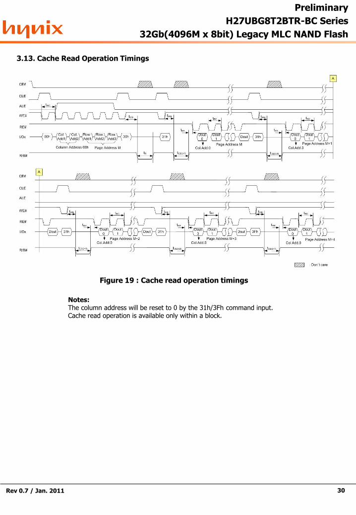
3.13. Cache Read Operation Timings
Figure 19 : Cache read operation timings
Notes: The column address will be reset to 0 by the 31h/3Fh command input.Cache read operation is available only within a block.

Preliminary
H27UBG8T2BTR-BC Series
32Gb(4096M x 8bit) Legacy MLC NAND Flash
Rev 0.7 / Jan. 2011 31
3.14. Multi Plane Cache Read Operation Timings
Figure 20 : Multi plane cache read operation Timings
Notes: 1. The column address will be reset to 0 by the 31h/3Fh command input.2. Cache read operation is available only within a block.3. Make sure to terminate the operation with 3Fh command. If the page read
operation is completed, issue FFh reset before next operation.4. Multi Plane Page addresses are required to be the same.5. Multi plane cache read must be used after Multi plane programmed page,
multi plane cache program, and multi plane copy-back program
Preliminary
H27UBG8T2BTR-BC Series
32Gb(4096M x 8bit) Legacy MLC NAND Flash
Rev 0.7 / Jan. 2011 32
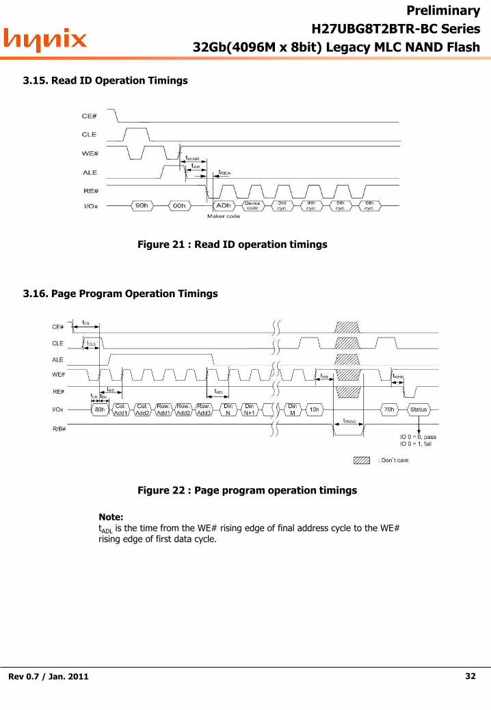
3.15. Read ID Operation Timings
Figure 21 : Read ID operation timings
3.16. Page Program Operation Timings
Figure 22 : Page program operation timings
Note:tADL is the time from the WE# rising edge of final address cycle to the WE# rising edge of first data cycle.

Preliminary
H27UBG8T2BTR-BC Series
32Gb(4096M x 8bit) Legacy MLC NAND Flash
Rev 0.7 / Jan. 2011 33
3.17. Page Program Operation Timings with CE# don’t care
Figure 23 : Page program operation timings with CE# don’t care
Note:tADL is the time from the WE# rising edge of final address cycle to the WE# rising edge of first data cycle.
3.18. Random Data Input Timings
Figure 24 : Random data input timings
Notes:1. tADL is the time from the WE# rising edge of final address cycle to the WE# rising
edge of first data cycle.2. Random data input can be performed in a page.

Preliminary
H27UBG8T2BTR-BC Series
32Gb(4096M x 8bit) Legacy MLC NAND Flash
Rev 0.7 / Jan. 2011 34
3.19. Multi Plane Page Program Operation Timings
Figure 25 : Multi plane page program operation timing
Notes: 1. Any command between 11h and 81h is prohibited except 70h, 78h, 75h and FFh2. tADL is the time from the WE# rising edge of final address cycle to the WE# rising edge
of first data cycle. 3. Multi Plane Page addresses are required to be the same.
CLE
WE#
ALE
R/B#
Col.
Add180h
Col.
Add2
Row.
Add1
Row.
Add2
Row.
Add3
Din
N
Din
N+1
Din
M11hI/Ox
CE#A
tDBSYtWB
CLE
WE#
ALE
R/B#
Col.
Add181h
Col.
Add2
Row.
Add1
Row.
Add2
Row.
Add3
Din
N
Din
N+1
Din
M10hI/Ox
CE#
A
tPROGtWB
70h Status
tWHR
RE#
tWC
A0-A13 : Valid
A14-A21 : Valid( Page M)
A22 : Fixed ‘Low’A23 ~ A33 : Valid (Block J)
A0-A13 : Valid
A14-A21 : Valid( Page M)
A22 : Fixed ‘High’A23 ~ A33 : Valid (Block K)
IO 0 = 0, pass
IO 0 = 1, fail
Don’t care
tADL
tADL

Preliminary
H27UBG8T2BTR-BC Series
32Gb(4096M x 8bit) Legacy MLC NAND Flash
Rev 0.7 / Jan. 2011 35
3.20. Copy-Back Program Operation Timings with Random Date Input
Figure 26 : Copyback program operation timing with random data input
Note: Copy back operation is allowed only within the same memory plane.
3.21. Cache Program Operation Timings
Figure 27 : Cache program operation timings
Note:tPROG = Program time for the last page + Program time for the (last -1)th page
- (command input cycle time + address input cycle time + Last page data loading time)

Preliminary
H27UBG8T2BTR-BC Series
32Gb(4096M x 8bit) Legacy MLC NAND Flash
Rev 0.7 / Jan. 2011 36
3.22. Multi Plane Cache Program Operation Timings
CLE
WE#
ALE
R/B#
Col.
Add180h
Col.
Add2
Row.
Add1
Row.
Add2
Row.
Add3
DIN
N
DIN
MI/Ox
CE#
tWC
tDBSY
11hCol.
Add181h
Col.
Add2
Row.
Add1
Row.
Add2
Row.
Add3
DIN
N
DIN
M
tWC
15h
A
tCBSYW
tWB
tADLtADL
: Don’t care
CLE
WE#
ALE
R/B#
Col.
Add180h
Col.
Add2
Row.
Add1
Row.
Add2
Row.
Add3
DIN
N
DIN
MI/Ox
CE#
tWC
tDBSY
11hCol.
Add181h
Col.
Add2
Row.
Add1
Row.
Add2
Row.
Add3
DIN
N
DIN
M
tWC
10h
A
tPROG
tWB
tADLtADL
A0-A13 : Valid
A14-A21 : Valid (Page M)
A22 : Fixed ‘Low’A23 ~ A33 : Valid (Block J)
A0-A13 : Valid
A14-A21 : Valid( Page M)
A22 : Fixed ‘High’A23 ~ A33 : Valid (Block K)
A0-A13 : Valid
A14-A21 : Valid( Page M+n)
A22 : Fixed ‘Low’A23 ~ A33 : Valid (Block J)
A0-A13 : Valid
A14-A21 : Valid( Page M+n)
A22 : Fixed ‘High’A23 ~ A33 : Valid (Block K)
Figure 28 : Multi plane cache program operation timings
Notes:1. tPROG = Program time for the last page + Program time for the (last -1)th page –
(command input cycle time + address input cycle time + Last page data loading time)2. Make sure to terminate the operation with 80h-10h- command sequence. If the operation is
terminated by 80h-15h command sequences, monitor I/O5 (Ready/Busy) and I/O6 (Data CacheReady/Busy) by issuing Read Status Command (70h) and make sure the previous and currentCache Page Program operation is completed. If the page program operation is completed, issueFFh reset before next operation.
3. Selected Page address except A22 within two blocks must be same.
3.23. Block Erase Operation Timings
Figure 29 : Block erase operation timings

Preliminary
H27UBG8T2BTR-BC Series
32Gb(4096M x 8bit) Legacy MLC NAND Flash
Rev 0.7 / Jan. 2011 37
3.24. Multi Plane Erase Operation Timings
CLE
WE#
ALE
R/B#
Row.
Add160h
Row.
Add2
Row.
Add360h
Row.
Add1
Row.
Add2
Row.
Add3D0hI/Ox
CE#
tWC
A14-A21 : Fixed ‘Low”
A22 : Fixed ‘Low’A23 ~ A33 : Valid (Block N)
70h Status
tBERS
A14-A21 : Fixed ‘Low”
A22 : Fixed ‘High’A23 ~ A33 : Valid (Block M)
RE#
tWB tWHR
IO 0 = 0, pass
IO 0 = 1, fail
: Don’t care
Figure 30 : Multi plane erase operation timings
3.25. Reset Timings
Figure 31 : Reset timings
Preliminary
H27UBG8T2BTR-BC Series
32Gb(4096M x 8bit) Legacy MLC NAND Flash
Rev 0.7 / Jan. 2011 38
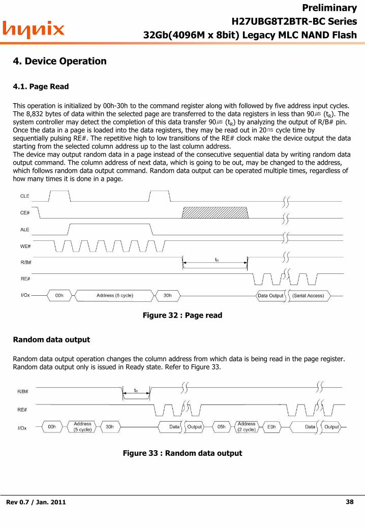
Figure 32 : Page read
Figure 33 : Random data output
4. Device Operation
4.1. Page Read
This operation is initialized by 00h-30h to the command register along with followed by five address input cycles. The 8,832 bytes of data within the selected page are transferred to the data registers in less than 90㎲ (tR). The system controller may detect the completion of this data transfer 90㎲ (tR) by analyzing the output of R/B# pin. Once the data in a page is loaded into the data registers, they may be read out in 20㎱ cycle time by sequentially pulsing RE#. The repetitive high to low transitions of the RE# clock make the device output the data starting from the selected column address up to the last column address.The device may output random data in a page instead of the consecutive sequential data by writing random data output command. The column address of next data, which is going to be out, may be changed to the address, which follows random data output command. Random data output can be operated multiple times, regardless of how many times it is done in a page.
Random data output
Random data output operation changes the column address from which data is being read in the page register. Random data output only is issued in Ready state. Refer to Figure 33.
Preliminary
H27UBG8T2BTR-BC Series
32Gb(4096M x 8bit) Legacy MLC NAND Flash
Rev 0.7 / Jan. 2011 39
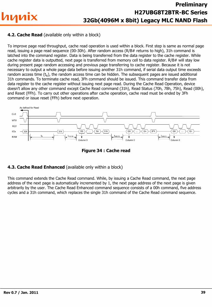
4.2. Cache Read (available only within a block)
To improve page read throughput, cache read operation is used within a block. First step is same as normal page read, issuing a page read sequence (00-30h). After random access (R/B# returns to high), 31h command is latched into the command register. Data is being transferred from the data register to the cache register. While cache register data is outputted, next page is transferred from memory cell to data register. R/B# will stay low during present page random accessing and previous page transferring to cache register. Because it is not necessary to output a whole page data before issuing another 31h command, if serial data output time exceeds random access time (tR), the random access time can be hidden. The subsequent pages are issued additional 31h commands. To terminate cache read, 3Fh command should be issued. This command transfer data from data register to the cache register without issuing next page read. During the Cache Read Operation, device doesn‟t allow any other command except Cache Read command (31h), Read Status (70h, 78h, 75h), Read (00h), and Reset (FFh). To carry out other operations after cache operation, cache read must be ended by 3Fh command or issue reset (FFh) before next operation.
Figure 34 : Cache read
4.3. Cache Read Enhanced (available only within a block)
This command extends the Cache Read command. While, by issuing a Cache Read command, the next page address of the next page is automatically incremented by 1, the next page address of the next page is given arbitrarily by the user. The Cache Read Enhanced command sequence consists of a 00h command, five address cycles and a 31h command, which replaces the single 31h command of the Cache Read command sequence.
Preliminary
H27UBG8T2BTR-BC Series
32Gb(4096M x 8bit) Legacy MLC NAND Flash
Rev 0.7 / Jan. 2011 40
Figure 35 : Multi plane page read
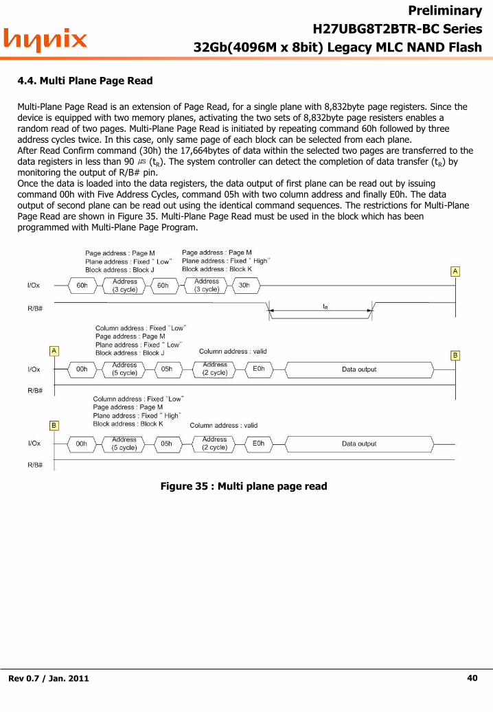
4.4. Multi Plane Page Read
Multi-Plane Page Read is an extension of Page Read, for a single plane with 8,832byte page registers. Since the device is equipped with two memory planes, activating the two sets of 8,832byte page resisters enables a random read of two pages. Multi-Plane Page Read is initiated by repeating command 60h followed by three address cycles twice. In this case, only same page of each block can be selected from each plane.After Read Confirm command (30h) the 17,664bytes of data within the selected two pages are transferred to the data registers in less than 90 ㎲ (tR). The system controller can detect the completion of data transfer (tR) by monitoring the output of R/B# pin.Once the data is loaded into the data registers, the data output of first plane can be read out by issuing command 00h with Five Address Cycles, command 05h with two column address and finally E0h. The data output of second plane can be read out using the identical command sequences. The restrictions for Multi-Plane Page Read are shown in Figure 35. Multi-Plane Page Read must be used in the block which has been programmed with Multi-Plane Page Program.
Preliminary
H27UBG8T2BTR-BC Series
32Gb(4096M x 8bit) Legacy MLC NAND Flash
Rev 0.7 / Jan. 2011 41
Figure 36 : Multi plane cache read
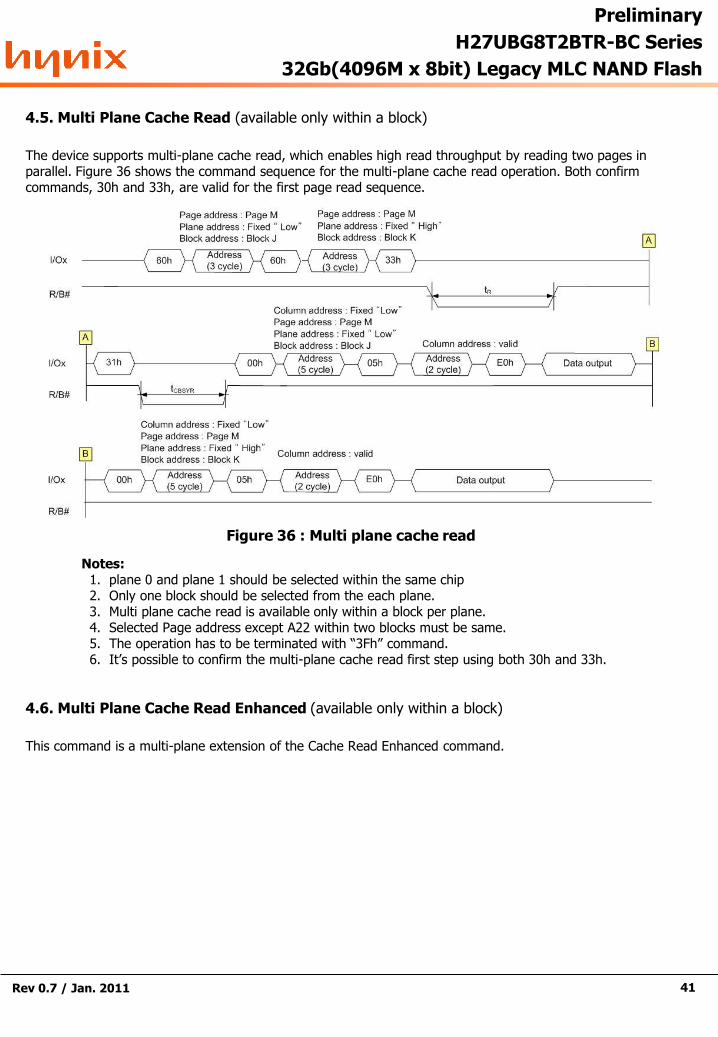
Notes:1. plane 0 and plane 1 should be selected within the same chip 2. Only one block should be selected from the each plane. 3. Multi plane cache read is available only within a block per plane. 4. Selected Page address except A22 within two blocks must be same.5. The operation has to be terminated with “3Fh” command.6. It‟s possible to confirm the multi-plane cache read first step using both 30h and 33h.
4.5. Multi Plane Cache Read (available only within a block)
The device supports multi-plane cache read, which enables high read throughput by reading two pages in parallel. Figure 36 shows the command sequence for the multi-plane cache read operation. Both confirm commands, 30h and 33h, are valid for the first page read sequence.
4.6. Multi Plane Cache Read Enhanced (available only within a block)
This command is a multi-plane extension of the Cache Read Enhanced command.

Preliminary
H27UBG8T2BTR-BC Series
32Gb(4096M x 8bit) Legacy MLC NAND Flash
Rev 0.7 / Jan. 2011 42
I/Ox 90h
CLE
WE#
RE#
ADh00h
ALE
DEh 94h D2h 04h 43h
tWHR
Figure 37 : Read ID
4.7. Read ID
The device contains a product identification mode, initiated by writing 90h to the command register, followed by an address input of 00h. Six read cycles sequentially output the manufacturer code (ADh), and the device code and 3rd, 4th, 5th, 6th cycle ID, respectively. The command register remains in Read ID mode until further commands are issued to it. Figure 37 shows the operation sequence, while 2.10 READ ID data tables explain the byte meaning.

Preliminary
H27UBG8T2BTR-BC Series
32Gb(4096M x 8bit) Legacy MLC NAND Flash
Rev 0.7 / Jan. 2011 43
4.8. Read Status Register
The device contains a Status Register which may be read to find out whether read, program or erase operation is completed, and whether the program or erase operation is completed successfully. After writing Read Status (70h) or Multi Plane Read Status (78h,75h) command to the command register, a read cycle outputs the content of the Status Register to the I/O pins only if CE# and RE# are low, whichever occurs last. This two line control allows the system to poll the progress of each device in multiple memory connections even when R/B# pins are common-wired. Refer to 2.8. STATUS REGISTER CODINGS for specific Status Register definitions and Figure 38, Figure 39 for Read Status. The command register remains in Read Status mode until further commands are issued to it. Therefore, if the status register is read during a random read cycle, the read command (00h) should be given before starting read cycles.
Figure 38 : Read status
Figure 39 : Multi plane read status

Preliminary
H27UBG8T2BTR-BC Series
32Gb(4096M x 8bit) Legacy MLC NAND Flash
Rev 0.7 / Jan. 2011 44
4.9. Page Program
The device is programmed as a page unit. The number of consecutive partial page programming operation within the same page without an intervening erase operation must not exceed 1 times. The program addressing should be done in sequential order in a block. A page program cycle consists of a serial data loading period in which up to 8,832 bytes of data may be loaded into the data register, followed by a non-volatile programming period where the loaded data is programmed into the appropriate cell. The serial data-loading period begins by inputting the Serial Data Input command (80h), followed by the five cycle address inputs and then serial data. The words other than those to be programmed do not need to be loaded. The device supports random data input in a page. The column address of next data, which will be entered, may be changed to the address which follows random data input command (85h). Random data input may be operated multiple times, regardless of how many times it is done in a page. The Page Program Confirm command (10h) initiates the programming process. Writing 10h alone without previously entering the serial data will not initiate the programming process. The internal write state controller automatically executes the algorithms and timings necessary for program and verify, thereby freeing the system controller for other tasks. Once the program process starts, the Read Status Register command may be entered to read the status register.The system controller can detect the completion of a program cycle by monitoring the R/B# output, or the Status bit (I/O 6) of the Status Register. Only the Read Status command and Reset command are valid while programming is in progress. The Write Status Bit (I/O 0) is valid, when all internal operations are complete (status bit I/O 6 = high).The internal write verify detects only errors for "1"s that are not successfully programmed to "0"s.The command register remains in Read Status command mode until another valid command is written to the command register. Figure 40 and Figure 41 details the sequence.
Figure 40 : Page Program
Figure 41 : Random data input

Preliminary
H27UBG8T2BTR-BC Series
32Gb(4096M x 8bit) Legacy MLC NAND Flash
Rev 0.7 / Jan. 2011 45
4.10. Multi Plane Program
Device supports multiple plane program. It is possible to program in parallel 2 pages, one per each plane.A multiple plane program cycle consists of a double serial data loading period in which up to 17,664bytes of data may be loaded into the data register, followed by a non-volatile programming period where the loaded data is programmed into the appropriate cell. The serial data loading period begins by inputting the Serial Data Input command (80h), followed by the five cycle address inputs and then serial data for the 1st page. Address for this page must be within first plane (A<22>=0). The data of first page other than those to be programmed do not need to be loaded. The device supports random data input exactly like page program operation. The Dummy Page Program Confirm command (11h) stops 1st page data input and the device becomes busy for a short time (tDBSY). Once it has become ready again, 81h command must be issued, followed by second page address (5 cycles) and its serial data input. Address for this page must be within second plane (A<22>=1). The data of second page other than those to be programmed do not need to be loaded. Program Confirm command (10h) makes parallel programming of both pages start. User can check operation status by R/B# pin or read status register command, as if it were a normal page program; status register command is also available during Dummy Busy time (tDBSY). In case of fail in first plane or second plane page program, fail bit of status register will be set: Pass/Fail status of each plane can be checked by Multi Plane Read Status. Figure 42 details the sequence.
Figure 42 : Multi plane page program
Notes: 1. plane 0 and plane 1 should be selected within the same chip 2. Only one block should be selected from the each plane. 3. Selected Page address except A22 within two blocks must be same.4. Any command between 11h and 81h is prohibited except 70h/78h/75h and FFh. 5. Read Status command can be 70h or 78h or 75h.

Preliminary
H27UBG8T2BTR-BC Series
32Gb(4096M x 8bit) Legacy MLC NAND Flash
Rev 0.7 / Jan. 2011 46
4.11. Cache Program (available only within a block)
Cache Program is an extension of the standard page program, which is executed with 8,832 bytes cache registers and same bytes data register. After the serial data input command (80h) is loaded to the command register, followed by 5 cycles of address, a full or partial page of data is latched into the cache register, and then the cache write command (15h) is loaded to the command register. After that sequence, the data in the cache register is transferred into the data register for cell programming. At this time, the device remains in busy state. After all data of the cache register is transferred into the data register, the device goes to the Ready state to load the next data into the cache register by issuing another cache program command sequence (80h-15h).There are some restrictions for cache program operation.1. The cache program command is available only within a block.2. User must give address and data after 80h command.The Busy time of first sequence equals the time it takes to transfer the data of cache register to the data register. Cell programming of the data of data register and loading of the next data into the cache register is consequently processed as a pipeline method. On the second and cascading sequence, transfer from the cache register to the data register is held off until cell programming of current data register contents has been done.Read Status command (70h) may be issued to find out when the cache register is ready by polling the Cache-Busy status bit (I/O 6). In addition, the status bit (I/O 5) can be used to determine when the cell programming of the current data register contents is complete. Pass/fail status of only the previous page (I/O 1) is available upon the return to Ready state.If the system monitors the progress of programming only with R/B#, the last page of the target programming sequence must be programmed with actual Page Program command (10h). If the Cache Program command (15h) is used instead, status bit (I/O5) must be polled to find out when the last programming is actually finished before starting other operations such as read. Pass/fail status is available in two steps. I/O 1 returns with the status of the previous page upon Ready or I/O6 status bit changing to "1", and later I/O 0 with the status of current page upon true Ready (returning from internal programming) or I/O 5 status bit changing to "1". I/O 1 may be read together when I/O 0 is checked. Refer to 2.8. Status Register Coding and Figure 43 for more details.

Preliminary
H27UBG8T2BTR-BC Series
32Gb(4096M x 8bit) Legacy MLC NAND Flash
Rev 0.7 / Jan. 2011 47
Figure 43 : Cache program

Preliminary
H27UBG8T2BTR-BC Series
32Gb(4096M x 8bit) Legacy MLC NAND Flash
Rev 0.7 / Jan. 2011 48
4.12. Multi Plane Cache Program (available only within a block)
The device supports multi-plane cache program, which enables high program throughput by programming two pages. The serial data-loading period begins by inputting the Serial Data Input command (80h), followed by the five cycle address inputs and then serial data for the first page. Address for this page must be within first plane (A<22>=0). The data of first page other than those to be programmed do not need to be loaded. The device supports random data input exactly like page program operation. The Dummy Page Program Confirm command (11h) stops 1st page data input and the device becomes busy for a short time (tDBSY). Once it has become ready again, 81h command must be issued, followed by 2nd page address (5 cycles) and its serial data input. Address for this page must be within second plane (A<22>=1). The data of second page other than those to be programmed do not need to be loaded. Cache Program Confirm command (15h) makes parallel programming of both pages start. And last page inputs Program confirm command (10h). Figure 44 shows the command sequence for Multi Plane Cache Program operation. After the “15h” or “10h” command, the result per plane of the operation is shown through the “78h” Multi Plane Read Status command.
Figure 44 : Multi plane cache program
Notes:1. plane 0 and plane 1 should be selected within the same chip 2. Only one block should be selected from the each plane. 3. Multi plane cache program is available only within a block per plane. 4. Selected Page address except A22 within two blocks must be same.5. The operation has to be terminated with “10h” command.6. Any command between 11h and 81h is prohibited except 70h/78h/75h and FFh.7. Read Status command can be 70h or 78h or 75h. Reading the Status per plane
is available only 78h.

Preliminary
H27UBG8T2BTR-BC Series
32Gb(4096M x 8bit) Legacy MLC NAND Flash
Rev 0.7 / Jan. 2011 49
4.13. Copy-Back Program
Copy-Back program with Read for Copy-Back is configured to quickly and efficiently rewrite data stored in one page without data reloading when the bit error is not in data stored. Since the time-consuming re-loading cycles are removed, the system performance is improved. The benefit is especially obvious when a portion of a block is updated and the rest of the block needs to be copied to the newly assigned free block. Copy-Back operation is a sequential execution of Read for Copy-Back and of copy-back program with the destination page address. A read operation with "35h" command and the address of the source page moves the whole 8,832byte data into the internal data buffer. A bit error is checked by sequential reading the data output. In the case where there is no bit error, the data do not need to be reloaded. Therefore, Copy-Back program operation is initiated by issuing Page-Copy Data-Input command (85h) with destination page address. Actual programming operation begins after Program Confirm command (10h) is issued. Once the program process starts, the Read Status Register command (70h) may be entered to read the status register. The system controller can detect the completion of a program cycle by monitoring the R/B# output, or the Status bit (I/O 6) of the Status Register. When the Copy-Back Program is complete, the Write Status Bit (I/O 0) may be checked. The command register remains in Read Status command mode until another valid command is written to the command register. During copy-back program, data modification is possible using random data input command (85h) as shown in Figure 45.
Figure 45 : Copy-back program

Preliminary
H27UBG8T2BTR-BC Series
32Gb(4096M x 8bit) Legacy MLC NAND Flash
Rev 0.7 / Jan. 2011 50
Figure 46 : Multi plane Copyback program
4.14. Multi-Plane Copy-Back Program
Multi-Plane Copy-Back Program is an extension of Copy-Back Program, for a single plane with 8,832byte page registers. Since the device is equipped with two memory planes, activating the two sets of 8,832byte page registers enables a simultaneous programming of two pages. Figure 46 and Figure 47 show command sequence for the multi-plane copy-back operation. First case, Figure 46, shows random data input of two planes that started right after finishing random data output of previous two planes. Second case, Figure 47, shows the random data input of each plane which started right after finishing the random data output of each plane

Preliminary
H27UBG8T2BTR-BC Series
32Gb(4096M x 8bit) Legacy MLC NAND Flash
Rev 0.7 / Jan. 2011 51
Figure 47 : Multi plane Copyback program
Figure 48 : Block Erase
4.15. Block Erase
The Erase operation is done on a block basis. Block address loading is accomplished in two cycles initiated by an Erase Setup command (60h). Only address A22 to A33 is valid while A14 to A21 is ignored. The Erase Confirm command (D0h) following the block address loading initiates the internal erasing process. This two-step sequence of setup followed by execution command ensures that memory contents are not accidentally erased due to external noise conditions.At the rising edge of WE# after the erase confirm command input, the internal write controller handles erase and erase verify.Once the erase process starts, the Read Status Register command may be entered to read the status register. The system controller can detect the completion of an erase by monitoring the R/B# output, or the Status bit (I/O 6) of the Status Register. Only the Read Status command and Reset command are valid while erasing is in progress. When the erase operation is completed, the Write Status Bit (I/O 0) may be checked. Figure 46 details the sequence.

Preliminary
H27UBG8T2BTR-BC Series
32Gb(4096M x 8bit) Legacy MLC NAND Flash
Rev 0.7 / Jan. 2011 52
Figure 49 : Multi plane Block Erase
Figure 50 : Reset
4.16. Multi Plane Block Erase
Multiple plane erase, allows parallel erase of two blocks, one per each memory plane.Block erase setup command (60h) must be repeated two times, each time followed by first block and second block address respectively (3 cycles each). As for block erase, D0h command makes embedded operation start. Multi plane erase does not need any Dummy Busy Time between first and second block address insertion. Address limitation required for Multiple Plane Program applies also to multiple plane erase, as well as operation progress can be checked like for Multiple Plane Program. Refer to the detail sequence as shown below.
4.17. Reset
The device offers a reset feature, executed by writing FFh to the command register. When the device is in Busy state during random read, program or erase mode, the reset operation will abort these operations. The contents of memory cells being altered are no longer valid, as the data will be partially programmed or erased. The command register is cleared to wait for the next command, and the Status Register is cleared to value E0h when WP# is high. Refer to 2.8. Status Register Coding for device status after reset operation. If the device is already in reset state, the command register will not accept a new reset command. The R/B# pin goes low for tRST after the Reset command is written. Refer to Figure 50.

Preliminary
H27UBG8T2BTR-BC Series
32Gb(4096M x 8bit) Legacy MLC NAND Flash
Rev 0.7 / Jan. 2011 53
5. Other Features
5.1. Data Protection & Power on/off Sequence
The device is designed to offer protection from any involuntary program/erase during power-transitions. An internal voltage detector disables all functions whenever VCC is below about 2.0V (3.3V device). WP# pin provides hardware protection and is recommended to be kept at VIL during power-up and power-down. The reset command (FFh) must be issued to all dies as the first command after device is power up. Each R/B# will be busy for maximum of 2ms after reset command is issued. In this time, the acceptable command is 70h or 78h or 75h.
Figure 51 : Data protection and power on / off

Preliminary
H27UBG8T2BTR-BC Series
32Gb(4096M x 8bit) Legacy MLC NAND Flash
Rev 0.7 / Jan. 2011 54
Figure 52 : Ready / Busy
5.2. Ready / Busy
The device has a Ready/Busy output that provides method of indicating the completion of a page program, erase, copy-back and random read completion. The R/B# pin is normally high and goes to low when the device is busy (after a reset, read, program, and erase operation). It returns to high when the internal controller has finished the operation. The pin is an open-drain driver thereby allowing two or more R/B# outputs to be Or-tied. Because pull-up resistor value is related to tR (R/B#) and current drain during busy (Ibusy), an appropriate value can be obtained with the following reference chart (Figure 52). Its value can be determined by the following guidance.

Preliminary
H27UBG8T2BTR-BC Series
32Gb(4096M x 8bit) Legacy MLC NAND Flash
Rev 0.7 / Jan. 2011 55
Figure 53 : Enable Programming
Figure 55 : Enable Erasing Figure 56 : Disable Erasing
Figure 54 : Disable Programming
5.3. Write Protect Operation
The Erase and Program Operations are automatically reset when WP# goes Low (tWW = 100ns, min). The operations are enabled and disabled as follows (Figure 53 ~ 56).

Preliminary
H27UBG8T2BTR-BC Series
32Gb(4096M x 8bit) Legacy MLC NAND Flash
Rev 0.7 / Jan. 2011 56
6. Application Notes and Comments
6.1. Paired Page Address Information

Preliminary
H27UBG8T2BTR-BC Series
32Gb(4096M x 8bit) Legacy MLC NAND Flash
Rev 0.7 / Jan. 2011 57
When program operation is abnormally aborted (ex. power-down, reset), not only page data under program but also a coupled row paired page data may be damaged. For example, during Page Program operation of page address 05h is aborted by reset or power down, the data of 00h, 01h, 04h, and 05h page address may be spoiled.
6.2. Acceptable Command after 80h
After Program Start Command (80h) is inputted, do not input any command except 85h, 10h, 11h, 15h, and FFh. If a command is inputted except these commands, the program operation cannot be executed.
6.3. Acceptable Command between Start command and Confirm command
Only Reset Command is available between start commands and confirm commands set (start command-address-confirm command style) that is mentioned in 1.7 Command Set. If other command is inputted, the operation cannot be executed. Do not input any commands except FFh. For instance, it is impossible to perform a normal Page Read operation, if any command is inputted between Page Read Command Set (00h - 5 address cycle - 30h).
6.4. Restriction of Read Status Value in Multi Plane Operation
During Multi plane operation, only 70h, 78h,75h and FFh are available between 11h-81h. But, the pass/fail output information of 70h and 78h and 75h is not valid. During this time, only ready / busy (I/O6 and I/O5) state can be checked. Refer to Figure 57.
Figure 57 : Restriction read status in multi plane operation
6.5. Page Program Failure
If the Page Program operation for page address N is fail, remain data in data register may be different to input data by host. Therefore, do not attempt to program the page address M in another block without the data input sequence. The same input sequence of 80h command, address and data is necessary.
6.6. Restriction Multi Plane Operation
To prevent abnormal multi plane operation, do not input bad block address to all Multi Plane Operation. Otherwise, the input data of valid block could be lost and the operation could be abnormally stopped.