data retention in mlc nand flash memory:...
TRANSCRIPT
1
Data Retention in MLC NAND Flash Memory:
Characterization, Optimization, and Recovery
Yu Cai, Yixin Luo, Erich F. Haratsch*, Ken Mai, Onur Mutlu Carnegie Mellon University, *LSI Corporation
[email protected], [email protected], [email protected], {kenmai, omutlu}@ece.cmu.edu
Abstract—Retention errors, caused by charge leakage over
time, are the dominant source of flash memory errors. Under-
standing, characterizing, and reducing retention errors can sig-
nificantly improve NAND flash memory reliability and endur-
ance. In this paper, we first characterize, with real 2y-nm MLC
NAND flash chips, how the threshold voltage distribution of flash
memory changes with different retention age – the length of time
since a flash cell was programmed. We observe from our charac-
terization results that 1) the optimal read reference voltage of a
flash cell, using which the data can be read with the lowest raw
bit error rate (RBER), systematically changes with its retention
age, and 2) different regions of flash memory can have different
retention ages, and hence different optimal read reference volt-
ages. Based on our findings, we propose two new techniques.
First, Retention Optimized Reading (ROR) adaptively learns and
applies the optimal read reference voltage for each flash memory
block online. The key idea of ROR is to periodically learn a tight
upper bound, and from there approach the optimal read refer-
ence voltage. Our evaluations show that ROR can extend flash
memory lifetime by 64% and reduce average error correction
latency by 10.1%, with only 768 KB storage overhead in flash
memory for a 512 GB flash-based SSD. Second, Retention Failure
Recovery (RFR) recovers data with uncorrectable errors offline
by identifying and probabilistically correcting flash cells with
retention errors. Our evaluation shows that RFR reduces RBER
by 50%, which essentially doubles the error correction capabil-
ity, and thus can effectively recover data from otherwise uncor-
rectable flash errors.
Keywords—NAND Flash Memory; Retention; Threshold Volt-
age Distribution; ECC; Fault Tolerance; Reliability;
1. Introduction
Over the past decade, the capacity of NAND flash memory has been increasing continuously, as a result of aggressive pro-cess scaling and the advent of multi-level cell (MLC) technol-ogy. This trend has enabled NAND flash memory to replace spinning disks for a wide range of applications – from high performance clusters and large-scale data centers to consumer PCs, laptops, and mobile devices. Unfortunately, as flash den-sity increases, flash memory cells become more vulnerable to various types of device and circuit level noise [1][2] – e.g., retention noise [2][3][4][5][6], read disturbance noise [5], cell-to-cell program interference noise [2][7][8], and program/erase (P/E) cycling noise [2][9]. These are sources of errors that can significantly degrade NAND flash reliability.
A traditional solution to overcome flash errors, regardless of their source, is to use error-correcting codes (ECC) [10][11]. By storing a certain amount of redundant bits per unit data, ECC can detect and correct a limited number of raw bit errors. With the help of ECC, flash memory can hide these errors from
the users until the number of errors per unit data exceeds the correction capability of the ECC. Flash memory designers have been relying on stronger ECC to compensate for lifetime re-ductions due to technology scaling. However, stronger ECC, which has higher capacity and implementation overhead, has diminishing returns on the amount of flash lifetime improve-ment [3][4]. As such, we intend to look for more efficient ways of reducing flash errors.
Retention errors, caused by charge leakage over time after a flash cell is programmed, are the dominant source of flash memory errors [2][3][4][12]. The amount of charge stored in a flash memory cell determines the threshold voltage level of the cell, which in turn represents the logical data value stored in the cell. The flash controller reads data from each cell by ap-plying several read reference voltages to the cell to identify its threshold voltage. As flash memory process technology scales to smaller feature sizes, the capacitance of a flash cell, and the number of electrons stored on it, decreases. State-of-the-art MLC flash memory cells can only store ~100 electrons. Gain-ing or losing several electrons on a flash cell can significantly change the cell’s voltage level and eventually alter the state of the cell. In addition, MLC technology reduces the size of the threshold voltage window [9], i.e., the span of threshold volt-age values corresponding to each logical state, in order to store more states in a single cell. This also makes the state of a cell more likely to shift due to charge loss caused by retention noise. As such, for flash memory, retention errors are one of the most important limiting factors of more aggressive process scaling and MLC technology.
One way to reduce retention errors is to periodically read, correct, and reprogram the flash memory before the number of errors accumulated over time exceed the error correction capa-bility of ECC [3][4][13][14]. However, this flash correct and refresh (FCR) technique has two major limitations: 1) FCR uses a fixed read reference voltage to read data under different retention ages, which is suboptimal (as we show in Sec. 3), and 2) FCR requires the flash controller to be consistently powered on so that errors can be corrected, limiting its applicability to enterprise deployments that have always-on power supplies.
In this paper, we pursue a better understanding of retention error behavior to improve NAND flash reliability and lifetime, and find better ways to mitigate flash retention errors. We characterize 1) the distortion of threshold voltage distribution at different retention ages for state-of-the-art 2y-nm (20- to 24-nm) NAND flash memory chips at room temperature, and 2) the retention age distribution of flash pages using disk traces taken from real workloads. Our key findings are: 1) Due to threshold voltage distribution distortion, the optimal read refer-ence voltages of flash cells, at which the minimum raw bit er-
2
ror rate (RBER) can be achieved, systematically shift to lower values as retention age increases. 2) Pages within the same flash block (the granularity at which flash memory can be erased) tend to have similar retention ages and hence similar optimal read reference voltages, whereas pages across different flash blocks have different optimal read reference voltages.
The key ideas of our approach leverage these findings to 1) optimize flash reliability, lifetime, and performance by learning and applying the optimal read reference voltage for each flash block online, and 2) recover uncorrectable flash errors that exceed the correction capability of ECC by identifying and correcting fast- and slow-leaking cells offline (by comparing the distortion of threshold voltages of different flash cells over different retention ages). Toward this end, we make the follow-ing three key contributions:
We are the first to characterize the distortion of threshold voltage distribution over different retention ages for 2y-nm NAND flash memory. We extensively analyze the correlation of this distortion with retention age and its implication on the optimal read reference voltage, raw bit error rate, and P/E cy-cles (Sec. 3).
We propose Retention Optimized Reading (ROR), a new online technique that reduces raw bit error rate by adaptively learning and applying the optimal read reference voltage for each flash block. Our evaluations show that ROR can extend flash lifetime by 64% and reduce average error correction la-tency by 10.1%, with only 768 KB storage overhead for a 512 GB flash-based SSD (Sec. 4).
We propose Retention Failure Recovery (RFR), a new offline error recovery technique that identifies fast- and slow-leaking cells and determines the original value of an erroneous cell based on its leakage-speed property and its threshold voltage. Our evaluations show that RFR can effectively reduce average RBER by 50%, essentially doubling the error correc-tion capability, which allows for the recovery of data other-wise uncorrectable by ECC (Sec. 5).
2. Background and Motivation
2.1. Basics of NAND Flash Memory
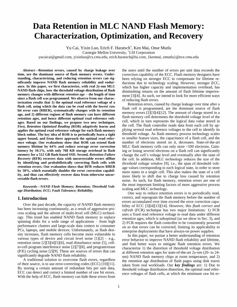
Fig. 1(a) shows the cross-sectional view of a flash cell. On top of a flash cell is the control gate (CG) and below is the floating gate (FG). The FG is insulated on both sides, on top by an inter-poly oxide layer and below by a tunnel oxide layer. As a result, the electrons programmed on the floating gate will not discharge even when flash memory is powered off.
Fig. 1. (a) Cross-sectional view of a flash cell, (b) retention loss mechanisms.
The voltage applied on the CG generates and controls the conductivity of the conductive channel between the source and the drain electrodes. The minimum voltage that can turn on the channel is called the threshold voltage. The threshold voltage
of a flash cell can be changed by injecting different amounts of charge onto the FG, whose generated electric field will partially cancel the electric field from the CG. Thus, the threshold voltage (Vth) of a flash cell can be formulated as [15]:
ppFGthith CQVV /)( (1)
In Eqn. 1, Vthi and Cpp are process-dependent constants. While QFG, the amount of charge that is programmed on the FG, is a variable. As Eqn. 1 shows, with more electrons (which carry negative charge) injected into the floating gate, the threshold voltage of the flash cell increases.
The threshold voltage range of a flash memory cell is divided into separate regions, with each of the regions representing a predefined binary n-bit value. As an example, for a 2-bit MLC NAND flash memory, the threshold voltage range is divided into four regions (erased, P1, P2, and P3 states), each of which corresponds to a unique 2-bit binary value. In MLC flash memory, the least significant bits are typi-cally organized together to form LSB pages, while the most significant bits form MSB pages.
Fowler-Nordheim (FN) tunneling. During a program op-eration, electrons are injected into the FG from the substrate when applying a high positive voltage (e.g., +10V) to the CG. During an erase operation, electrons are ejected from the FG into the substrate when applying a high negative voltage (e.g., ‒20V) to the CG. The injection and ejection of electrons through the tunnel oxide are enabled by the well-known Fowler-Nordheim (FN) tunneling effect [16], whose resulting tunneling current (JFN) [15] can be modeled as:
oxFN E
oxFNFN eEJ/2
(2)
In Eqn. 2, JFN is the tunneling current density, αFN and βFN
are constants, and Eox is the electric field strength in the tunnel oxide. As Eqn. 2 shows, the tunneling current (JFN) exponentially correlates with the oxide electric field strength (Eox).
When no external voltage is applied to any of the electrodes (i.e., CG, source, and drain) of a flash cell, an electric field still exists between the FG and the substrate, generated by the charge present in the FG. This is called the intrinsic electric field [15] (illustrated in Fig. 1a), and is expressed as:
oxthithoxonoonoox TVVCCCE /)()}/({ (3)
In Eqn. 3, Tox and Vthi are process-dependent constants. This intrinsic electric field generates stress-induced leakage current (SILC) [17][18], a weak tunneling current that leaks charge away from the FG.
2.2. Retention Loss Mechanisms
Retention loss is the phenomenon that the threshold voltage changes over time without external stimulation. It is caused by the unavoidable trapping of charge within the tunnel oxide [19]. The amount of trapped charge increases with the electri-cal stress induced by repeated program and erase operations, which degrade the insulating property of the tunnel oxide. We next explain two failure mechanisms (illustrated in Fig. 1b), which directly lead to retention loss.
Trap-assisted tunneling (TAT). The electric charge trapped in the tunnel oxide forms an electrical tunnel, which exacerbates the weak tunneling current, SILC. As a result of this TAT effect, the electrons present in the FG leak away
3
much faster through the intrinsic electric field. Hence, the threshold voltage of the flash cell decreases over time. As the flash cell wears out with increasing P/E cycles, the amount of trapped charge also increases [19], and so does the TAT effect. At high P/E cycles, the amount of trapped charge is large enough to form percolation paths that will significantly hamper the insulating properties of the gate dielectric [18], resulting in retention failure.
Charge de-trapping. The electric charge trapped in the tunnel oxide can also be spontaneously de-trapped over time [19][20][21]. Note that the polarity of the trapped charge can be either negative (i.e., electrons) or positive (i.e., holes). Hence, charge de-trapping can either decrease or increase the threshold voltage of a flash cell, depending on the polarity of the de-trapped charge.
2.3. Our Goal
The goal of this paper is threefold. First, we would like to build a strong understanding, characterization, and analysis of how the threshold voltage distribution of flash memory distorts over retention age, via experiments on and measurements of real NAND flash memory chips. Second, based on this under-standing, we aim to devise a new technique that optimizes the read reference voltage for data under different retention ages to minimize the raw bit error rate, and thus improve both the lifetime and system performance of flash memory. Third, we aim to devise a new mechanism that takes advantage of the unique charge-leakage properties of each individual flash cell, to recover the data that otherwise cannot be corrected by ECC due to the accumulated retention errors.
3. Retention Loss Characterization
In this section, we use the methodology described in Sec. 3.1 to characterize the effect of retention age on the threshold voltage distribution (Sec. 3.2), and its implications for the optimal read reference voltage (Sec. 3.3), RBER (Sec. 3.4), and P/E-cycle lifetime (Sec. 3.5). We make eight findings through-out our analysis, which motivate and inspire two new techniques proposed in Sec. 4 and Sec. 5.
3.1. Methodology
Testing platform. We use an FPGA-based flash memory testing platform [22] that allows us to issue commands to raw flash chips without ECC. We test 2-bit MLC NAND flash memory devices manufactured in 2y-nm technology. We use the read-retry feature present in these devices to accurately measure the threshold voltage of each cell [9]. Our previous works describe our testing platform in detail [2][3][4][7][8][9][22].
Temperature. We characterize the threshold voltage distributions over different retention ages and different P/E cycles at room temperature (20°C) to mimic real-world scenarios. While it is possible to accelerate retention tests under high temperature and compute the equivalent retention age under room temperature with the Arrhenius Law [22] (as done in [6]), we believe this method does not accurately represent how NAND flash memories are typically used, as it may exaggerate some causes of retention loss over others [24].
Tests. To characterize the threshold voltage distribution over different P/E cycles, we form multiple groups of flash
blocks, and repeatedly erase and program them with random data1 to different predefined P/E-cycle targets. Note that each group is set to a different P/E-cycle target to cover a collective range of 0 to 50,000 P/E cycles. To characterize the threshold voltage distribution over different retention ages, we first program predefined data to each block. Then, using the read reference voltage sweeping methodology [7][9][22], we read and record the threshold voltage distribution of all flash blocks after a certain retention age (i.e., a range of times from 1 day to 40 days) at room temperature. We use a 5-second dwell time2 for all tests.
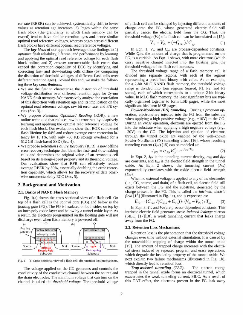
We first use the characterization results from a single repre-sentative group at 8k P/E cycles to demonstrate several trends and findings related to the threshold voltage distribution (Figs. 2-4), the optimal read reference voltage (Fig. 5), and RBER (Fig. 6). Note that similar trends and findings hold at different P/E cycles. Then, we use the characterization results from all of the groups to show trends and findings related to flash lifetime (Fig. 7).
3.2. Threshold Voltage Distribution under Retention Loss
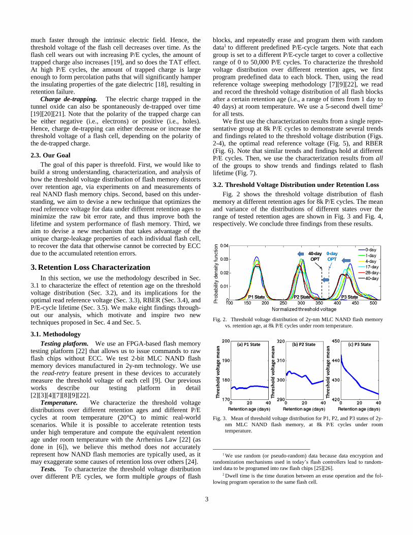
Fig. 2 shows the threshold voltage distribution of flash memory at different retention ages for 8k P/E cycles. The mean and variance of the distributions of different states over the range of tested retention ages are shown in Fig. 3 and Fig. 4, respectively. We conclude three findings from these results.
Fig. 2. Threshold voltage distribution of 2y-nm MLC NAND flash memory
vs. retention age, at 8k P/E cycles under room temperature.
Fig. 3. Mean of threshold voltage distribution for P1, P2, and P3 states of 2y-
nm MLC NAND flash memory, at 8k P/E cycles under room
temperature.
1 We use random (or pseudo-random) data because data encryption and
randomization mechanisms used in today’s flash controllers lead to random-
ized data to be programed into raw flash chips [25][26]. 2 Dwell time is the time duration between an erase operation and the fol-
lowing program operation to the same flash cell.
4
Fig. 4. Variance of threshold voltage distribution for P1, P2, and P3 states of
2y-nm MLC NAND flash memory, at 8k P/E cycles under room
temperature.
Finding 1: The threshold voltage distributions of the P2 and P3 states systematically shift to lower voltages with retention age.
In Fig. 2, we observe that the peaks of the P2 and P3 threshold voltage distributions shift to the left as retention age increases. Fig. 3 further verifies this observation quantitatively – the mean values of the P2 and P3 threshold voltage distributions decrease as retention age increases. However, the same observation does not apply to the P1 state. Fig. 3 shows that for the P1 state, the mean of the threshold voltage distribu-tion remains almost constant.
As discussed in Sec. 2.2, flash retention loss is caused by a combination of two mechanisms, TAT and charge de-trapping. Charge de-trapping can either increase or decrease the threshold voltage, depending on the polarity of the de-trapped charge. In contrast, TAT can only decrease the threshold voltage, as the resulting SILC can flow only in the direction of the intrinsic electric field generated by the electrons in the FG. In the P2 and P3 states, the intrinsic electric field strength is higher, making TAT the dominant source of retention loss. This explains why we observe the systematic decrease of threshold voltage with retention age.
Finding 2: The threshold voltage distribution of each state becomes wider with higher retention age.
In Fig. 2, the threshold voltage distribution of each state becomes wider as retention age increases. Fig. 4 further shows this observation quantitatively – the variance of all three threshold voltage distributions increases with retention age. 3
This trend can be caused by two reasons. First, charge de-trapping can either increase or decrease the threshold voltage. Some flash cells with higher threshold voltages (relative to the mean threshold voltage of the corresponding state) might gain charge over time, while some others with lower threshold voltages might lose charge. Second, process variation can cause TAT to decrease threshold voltages at different rates. Some flash cells with higher threshold voltages might leak charge slower due to TAT, while some others with lower threshold voltages might leak charge faster. As a result of both reasons, the threshold voltage distributions become wider and flatter over time.
3 Note that the P3 state experiences a downward spike of threshold volt-
age variance at low retention ages. This is because a significant number of
fast-leaking cells are initially programmed to higher voltages than the mean,
and thus move closer to the mean at low retention ages.
Finding 3: The threshold voltage distribution of a higher-voltage state shifts faster than that of a lower-voltage state.
In Fig. 3, the slope of the mean threshold voltage change with retention age is steeper for a higher-voltage state than that for a lower-voltage state (ΔP3>ΔP2>ΔP1). We have observed in Finding 1 that the threshold voltage distributions of the P2 and P3 states systematically shift to lower voltages with retention age, and that this slope indicates the speed of the observed shift with retention age.4
As discussed earlier, the systematic decrease of threshold voltage is caused by TAT, which exacerbates the tunneling current, SILC. SILC flows in the direction of the intrinsic electric field, and its magnitude exponentially correlates with the intensity of the intrinsic electric field (as shown in Eqn. 2). Furthermore, the intrinsic electric field intensity is proportional to the threshold voltage of the cell (as shown in Eqn. 3). As a result, a higher-voltage cell experiences a greater amount of SILC, and hence a faster drop in its threshold voltage.
3.3. Optimal Read Reference Voltage
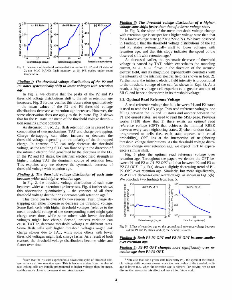
A read reference voltage that falls between P1 and P2 states is used to read the LSB page. Two read reference voltages, one falling between the P2 and P3 states and another between the P1 and erased states, are used to read the MSB page. Previous works [7][8] show that 1) there exists an optimal read reference voltage (OPT) that achieves the minimal RBER between every two neighboring states, 2) when random data is programmed to cells (i.e., each state appears with equal probability), OPT lies at the intersection of neighboring threshold voltage distributions. As the threshold voltage distri-butions change over retention age, we expect OPT to experi-ence a similar shift.
Fig. 5 plots the optimal read reference voltage over retention age. Throughout the paper, we denote the OPT be-tween P1 and P2 as P1-P2 OPT and that between P2 and P3 as P2-P3 OPT. Fig. 5(a) shows a slightly decreasing trend of P1-P2 OPT over retention age. Similarly, but more significantly, P2-P3 OPT decreases over retention age, as shown in Fig. 5(b). We conclude two findings from Fig. 5.
Fig. 5. Effect of retention age on the optimal read reference voltage between
(a) the P1 and P2 states, and (b) the P2 and P3 states.
Finding 4: Both P1-P2 OPT and P2-P3 OPT become smaller over retention age.
Finding 5: P2-P3 OPT changes more significantly over re-tention age than P1-P2 OPT.
4 Note also that, for a given state (especially P3), the speed of the thresh-
old voltage shift becomes slower when the mean value of the threshold volt-
age is lower (i.e., when the retention age is higher). For brevity, we do not
discuss the reasons for this effect and leave it for future work.

5
Since the distribution of the P1 state becomes wider without systematic shifts, the intersection of the P1 and P2 states tends to move to the right (assuming that the distribution of the P2 state does not change). On the other hand, since the threshold voltage distribution of the P2 state shifts to the left, the intersection between the P1 and P2 state distributions tends to shift to the left (assuming the distribution of the P1 state does not change). These two trends counteract each other, and thus P1-P2 OPT shifts only slightly to the left.
On the other hand, the distributions of the P2 and P3 states both shift to the left, and the amount of the distribution shift for the P3 state is larger than that of the P2 state (as can be seen in Fig. 3). Therefore, the intersection of the P2 and P3 states systematically shifts to the left. As such, P2-P3 OPT becomes smaller with retention age.
3.4. RBER for Suboptimal Read Reference Voltages
We have shown in Finding 4 that the optimal read reference voltages can be significantly different for different retention ages. Traditionally, the flash controller uses a fixed read refer-ence voltage for the entire flash memory, and is unaware of the distribution distortion caused by retention age. Such a fixed read reference voltage cannot be optimal for all blocks in flash memory due to two reasons. First, the retention age of an indi-vidual block varies over time due to both environmental factors that might change rapidly (e.g., temperature), causing varying amounts of retention loss, and the changing pattern of accesses the block receives. Second, different blocks are likely to be programmed at different times, and thus are likely to have dif-ferent retention ages.
To quantify how the choice of read reference voltage af-fects RBER, we apply the optimal read reference voltages (OPTs) determined for {0, 1, 2, 6, 9, 17, 21, 28}-day retention ages to read 28-day-old data. Fig. 6 shows the RBER obtained when reading the 28-day-old data with different OPTs, normal-ized to the RBER obtained when reading the data with the 28-day OPT. We conclude two major findings from Fig. 6.
Fig. 6. Normalized RBER when reading 28-day-old data with different
optimal read reference voltages (normalized to 28-day OPT).
Finding 6: The optimal read reference voltage corresponding to one retention age is suboptimal (i.e., it results in a higher RBER) for reading data with a different retention age.
For example, the RBER obtained when reading with 0-day OPT is 4.6 times higher than the RBER obtained when reading with the actual optimal read reference voltage (28-day OPT) for a retention age of 28 days.
Finding 7: RBER becomes lower when the retention age for which the used read reference voltage is optimized becomes closer to the actual retention age of the data.
Fig. 6 shows that RBER decreases when the applied OPT (as a function of retention age) becomes closer to the actual OPT for the data. Our previous work [8] shows that RBER reduces as we apply a read reference voltage closer to the OPT. For example, the RBER of 28-day-old data when reading it
with the 17-day OPT is only about 50% of that when reading it with the 6-day OPT. Combining this Finding 7 with Finding 4, which implies a monotonic relationship between OPT and re-tention age, we conclude that one can reduce RBER by esti-mating and applying the OPT that corresponds to the actual retention age of the data.
3.5. Lifetime vs. RBER
As RBER is affected by the applied read reference voltage,
flash memory lifetime also changes correspondingly with the
applied read reference voltage. In Fig. 7, we show RBER over
P/E cycles and the corresponding impact on flash lifetime, as-
suming all data has a 7-day retention age and is read with the
OPT for {0-7}-day retention ages. A typical flash device is
considered to be error-free if it guarantees an uncorrectable
error rate of less than 10-15, which corresponds to traditional
data storage reliability requirements [27]. For an ECC that can
correct up to 40 erroneous bits for every 1 KB of data, the ac-
ceptable RBER to meet this reliability requirement is 10-3
(shown by the horizontal dashed line in Fig. 7). We conclude
one finding from Fig. 7.
Fig. 7. RBER for 7-day-old data read using the optimal read reference
voltages of different retention ages, over P/E cycles.
Finding 8: The P/E-cycle lifetime of flash memory can be extended if the optimal read reference voltage that corre-sponds to the retention age of the data is used.
Fig. 7 divides the P/E-cycle lifetime of flash memory into
three stages, according to whether or not the RBER can be
tolerated by ECC when different read reference voltages are
applied. In Stage-0, all the errors are correctable by ECC when
any read reference voltage (i.e., 0-day OPT to 7-day OPT) is
applied. In Stage-1, the 7-day OPT yields an RBER that is cor-
rectable by ECC, while all other read reference voltages result
in unacceptable RBERs. In Stage-2, all read reference voltages
fail to guarantee an RBER that is correctable by ECC, and
hence flash memory comes to the end of its lifetime.
Note that, similar to Finding 7, as the retention age for
which the used read reference voltage is optimized gets closer
to the actual retention age of the data, RBER decreases (at any
given P/E cycle). Hence, the resulting flash lifetime also im-
proves correspondingly as the applied read reference voltage
approaches the actual OPT of the data (7-day OPT).
We conclude that if we actually apply the 7-day OPT when
reading data with 7-day retention age (i.e., when we apply the
OPT corresponding to the retention age of the data), RBER
reduces in Stage-0 (Finding 7) and flash lifetime improves in
Stage-1 (Finding 8). In Sec. 4, we will show that, when RBER
becomes lower, flash read latency also reduces (in both stages).
This strongly motivates us to estimate the actual OPT of the
6
Read flash memory
Error Correction
Corrected?Yes
Success
No
Select next VREF
Next VREF? NoYes
Fail
1
2
3
4
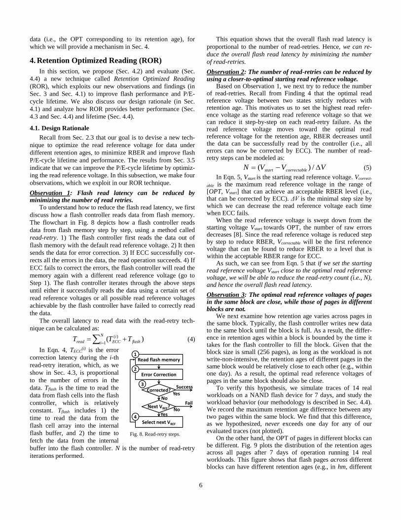
Fig. 8. Read-retry steps.
data (i.e., the OPT corresponding to its retention age), for
which we will provide a mechanism in Sec. 4.
4. Retention Optimized Reading (ROR)
In this section, we propose (Sec. 4.2) and evaluate (Sec.
4.4) a new technique called Retention Optimized Reading
(ROR), which exploits our new observations and findings (in
Sec. 3 and Sec. 4.1) to improve flash performance and P/E-
cycle lifetime. We also discuss our design rationale (in Sec.
4.1) and analyze how ROR provides better performance (Sec.
4.3 and Sec. 4.4) and lifetime (Sec. 4.4).
4.1. Design Rationale
Recall from Sec. 2.3 that our goal is to devise a new tech-
nique to optimize the read reference voltage for data under
different retention ages, to minimize RBER and improve flash
P/E-cycle lifetime and performance. The results from Sec. 3.5
indicate that we can improve the P/E-cycle lifetime by optimiz-
ing the read reference voltage. In this subsection, we make four
observations, which we exploit in our ROR technique.
Observation 1: Flash read latency can be reduced by minimizing the number of read retries.
To understand how to reduce the flash read latency, we first
discuss how a flash controller reads data from flash memory.
The flowchart in Fig. 8 depicts how a flash controller reads
data from flash memory step by step, using a method called
read-retry. 1) The flash controller first reads the data out of
flash memory with the default read reference voltage. 2) It then
sends the data for error correction. 3) If ECC successfully cor-
rects all the errors in the data, the read operation succeeds. 4) If
ECC fails to correct the errors, the flash controller will read the
memory again with a different read reference voltage (go to
Step 1). The flash controller iterates through the above steps
until either it successfully reads the data using a certain set of
read reference voltages or all possible read reference voltages
achievable by the flash controller have failed to correctly read
the data.
The overall latency to read data with the read-retry tech-
nique can be calculated as:
N
i flash
i
ECCread TTT1
)( )( (4)
In Eqn. 4, TECC(i) is the error
correction latency during the i-th
read-retry iteration, which, as we
show in Sec. 4.3, is proportional
to the number of errors in the
data. Tflash is the time to read the
data from flash cells into the flash
controller, which is relatively
constant. Tflash includes 1) the
time to read the data from the
flash cell array into the internal
flash buffer, and 2) the time to
fetch the data from the internal
buffer into the flash controller. N is the number of read-retry
iterations performed.
This equation shows that the overall flash read latency is
proportional to the number of read-retries. Hence, we can re-
duce the overall flash read latency by minimizing the number
of read-retries.
Observation 2: The number of read-retries can be reduced by using a closer-to-optimal starting read reference voltage.
Based on Observation 1, we next try to reduce the number of read-retries. Recall from Finding 4 that the optimal read reference voltage between two states strictly reduces with retention age. This motivates us to set the highest read refer-ence voltage as the starting read reference voltage so that we can reduce it step-by-step on each read-retry failure. As the read reference voltage moves toward the optimal read reference voltage for the retention age, RBER decreases until the data can be successfully read by the controller (i.e., all errors can now be corrected by ECC). The number of read-retry steps can be modeled as:
VVVN ecorrectablstart /)( (5)
In Eqn. 5, Vstart is the starting read reference voltage. Vcorrect-
able is the maximum read reference voltage in the range of [OPT, Vstart] that can achieve an acceptable RBER level (i.e., that can be corrected by ECC). ΔV is the minimal step size by which we can decrease the read reference voltage each time when ECC fails.
When the read reference voltage is swept down from the starting voltage Vstart
towards OPT, the number of raw errors decreases [8]. Since the read reference voltage is reduced step by step to reduce RBER, Vcorrectable will be the first reference voltage that can be found to reduce RBER to a level that is within the acceptable RBER range for ECC.
As such, we can see from Eqn. 5 that if we set the starting read reference voltage Vstart close to the optimal read reference voltage, we will be able to reduce the read-retry count (i.e., N), and hence the overall flash read latency.
Observation 3: The optimal read reference voltages of pages in the same block are close, while those of pages in different blocks are not.
We next examine how retention age varies across pages in the same block. Typically, the flash controller writes new data to the same block until the block is full. As a result, the differ-ence in retention ages within a block is bounded by the time it takes for the flash controller to fill the block. Given that the block size is small (256 pages), as long as the workload is not write-non-intensive, the retention ages of different pages in the same block would be relatively close to each other (e.g., within one day). As a result, the optimal read reference voltages of pages in the same block should also be close.
To verify this hypothesis, we simulate traces of 14 real workloads on a NAND flash device for 7 days, and study the workload behavior (our methodology is described in Sec. 4.4). We record the maximum retention age difference between any two pages within the same block. We find that this difference, as we hypothesized, never exceeds one day for any of our evaluated traces (not plotted).
On the other hand, the OPT of pages in different blocks can be different. Fig. 9 plots the distribution of the retention ages across all pages after 7 days of operation running 14 real workloads. This figure shows that flash pages across different blocks can have different retention ages (e.g., in hm, different
7
pages have retention ages ranging from 1 to 6 days), even though pages within the same block have similar retention ages. Recall from Finding 6 that data with different retention ages have different optimal read reference voltages. As such, this observation motivates us to record the optimal read reference voltages at a flash block (instead of a smaller page or a larger region) granularity.
Fig. 9. Retention age distribution across all pages after 7 days of operation.
Observation 4: The optimal read reference voltage of pages in a block is upper-bounded by the optimal read reference volt-age of the last-programmed page.
Within a page, the data in a flash block is programmed in page order (i.e., sequentially from page 0 to page 255, assum-ing 256 pages per block) to minimize inter-page program inter-ference [7]. Therefore, according to Finding 4, the optimal read reference voltage for page 255 is no less than that of any other page within the same block (because page 255 is programmed last and thus has the largest retention age). Hence, if we record the optimal read reference voltage of the last-programmed page (page 255), we can get the upper bound of the optimal read reference voltages of all pages in a given block.5
4.2. Retention Optimized Reading Mechanism
Next, we propose the Retention Optimized Reading (ROR) technique, which aims to reduce RBER by finding and using OPT for each block. ROR consists of two components: 1) an online pre-optimization algorithm triggered daily and after power-on to learn the starting read reference voltage for each block, and 2) an improved read-retry technique that uses the starting read reference voltage to approach OPT for the block.
Online pre-optimization algorithm. Motivated by our findings and observations in Sec. 3 and Sec. 4.1, we propose an online pre-optimization algorithm to learn and record OPT for the last-programmed page (i.e., page 255) in each block. As discussed earlier, this recorded reference voltage is a tight up-per bound of OPT for the block and hence can be used as the starting read reference voltage. The proposed algorithm con-sists of the following four steps.
Step 1 – Initialization. The flash controller first reads page 255 with any default read reference voltage Vdefault, and at-tempts to correct the errors in the raw data read from the page. Next, we record the number of raw bit errors as the currently lowest error count NERR, and the applied read reference voltage as Vref = Vdefault. If we cannot find the error count (i.e., the error is uncorrectable), we record the maximum number of errors correctable by ECC as NERR.
Step 2 – Try with a lower read reference voltage. Since we want to find the optimal read reference voltage for page 255 (Observation 4), we approach it from the current starting read
5 Note that even if a page is read in the future after it is programmed, its
optimal read reference voltage will decrease over time until it is read and thus
will never exceed this upper bound.
reference voltage step by step. Since OPT typically decreases over retention age (Finding 4), we first attempt to lower the read reference voltage. We decrease the read reference voltage to (Vref − ΔV) and read page 255. If the number of corrected errors in the new data is less than or equal to the old NERR, we update NERR and Vref with the new values. We repeat Step 2 until the number of corrected errors in the new data is greater than the old NERR or the lowest possible read reference voltage is reached.
Step 3 – Try with a higher read reference voltage. Since the optimal threshold voltage might increase in rare cases, we also attempt to increase the read reference voltage. We increase the read reference voltage to (Vref + ΔV) and read page 255. Again, if the number of corrected errors in the new data is less than or equal to NERR, we update NERR and Vref with the new values. We repeat Step 3 until the number of corrected errors in the new data is greater than the old NERR or the highest possible read reference voltage is reached.
Step 4 – Record the optimal read reference voltage. After Step 3, the currently used Vref is the optimal read reference voltage for page 255. Thus, we record this voltage as the upper bound of the optimal read reference voltages for the block.
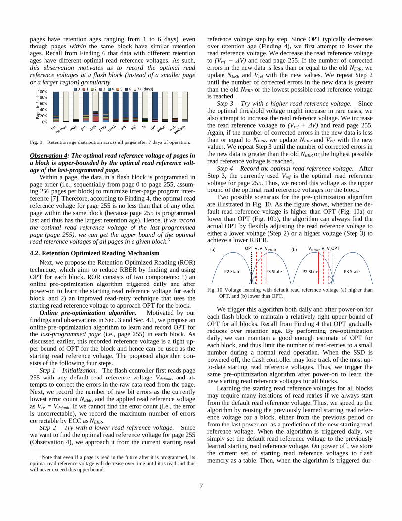
Two possible scenarios for the pre-optimization algorithm are illustrated in Fig. 10. As the figure shows, whether the de-fault read reference voltage is higher than OPT (Fig. 10a) or lower than OPT (Fig. 10b), the algorithm can always find the actual OPT by flexibly adjusting the read reference voltage to either a lower voltage (Step 2) or a higher voltage (Step 3) to achieve a lower RBER.
Fig. 10. Voltage learning with default read reference voltage (a) higher than
OPT, and (b) lower than OPT.
We trigger this algorithm both daily and after power-on for each flash block to maintain a relatively tight upper bound of OPT for all blocks. Recall from Finding 4 that OPT gradually reduces over retention age. By performing pre-optimization daily, we can maintain a good enough estimate of OPT for each block, and thus limit the number of read-retries to a small number during a normal read operation. When the SSD is powered off, the flash controller may lose track of the most up-to-date starting read reference voltages. Thus, we trigger the same pre-optimization algorithm after power-on to learn the new starting read reference voltages for all blocks.
Learning the starting read reference voltages for all blocks may require many iterations of read-retries if we always start from the default read reference voltage. Thus, we speed up the algorithm by reusing the previously learned starting read refer-ence voltage for a block, either from the previous period or from the last power-on, as a prediction of the new starting read reference voltage. When the algorithm is triggered daily, we simply set the default read reference voltage to the previously learned starting read reference voltage. On power off, we store the current set of starting read reference voltages to flash memory as a table. Then, when the algorithm is triggered dur-
8
ing power-on, we use the stored read reference voltages as the default read reference voltages.
Improved read-retry technique. During a normal read op-eration, we apply an improved read-retry technique that takes advantage of the recorded starting read reference voltage and Observation 4. First, the flash controller attempts to read the data with the recorded starting read reference voltage. Then, since the recorded starting read reference voltage is the upper bound of the OPTs within the block, we iteratively decrease the read reference voltage until the read operation succeeds. Note that the starting read reference voltages are accessed frequently (on each read operation) by the flash controller, so we store them in the SSD’s DRAM buffer to allow fast access. Com-pared with the original read-retry technique (Sec. 4.1), our technique is faster due to two reasons as it uses more infor-mation based on our findings: 1) it starts the read-retry process at an already close-to-optimal starting read reference voltage that is estimated and recorded daily and upon power-on, 2) it approaches OPT in a known, informed direction from this starting read reference voltage.
4.3. Minimizing the Error Correction Latency
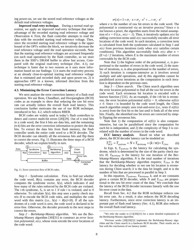
We next analyze the error correction latency of a flash read operation. We use Bose, Chaudhuri, and Hocquenghem (BCH) codes as an example to show that reducing the raw bit error rate can actually reduce the overall flash read latency. This conclusion further motivates the use of our ROR technique, introduced in Sec. 4.2, which reduces RBER.
BCH codes are widely used in today’s flash controllers to detect and correct multi-bit errors [28][29]. Out of n total bits in a code word, the first k bits are data bits, and the remaining (n-k) bits are the error correction information to protect the data bits. To extract the data bits from flash memory, the flash controller sends the entire code word to a BCH decoder. The BCH decoder can identify all the erroneous bits and flip them to correct the errors. Fig. 11 illustrates the three steps of a BCH decoder, which we explain briefly in turn.
Fig. 11. Error correction flow of BCH codes.
Step 1 – Syndrome calculation. First, to find out whether the code word, R(x), contains any error, the BCH decoder computes the syndrome vector, S(x), which indicates if and how many of the rules enforced by the BCH code are violated. The i-th syndrome, Si, is set to 1 if rule i is violated, and to 0 otherwise. To calculate S(x), this step uses a parity check ma-trix H to encode the BCH code rules, and multiplies the code word with this matrix (i.e., S(x) = R(x)×H). If all the syn-dromes of a code word is zero, the code word is declared to be error-free. Otherwise, the decoder proceeds to the next steps to correct the errors.
Step 2 – Berlekamp-Massey algorithm. We use the Ber-lekamp-Massey algorithm [30][31] to construct an error loca-tion polynomial, σ(x), whose roots encode the error locations of the code word:
e
e xxxx ...1)( 2
21
where e is the number of raw bit errors in the code word. The polynomial is constructed via an iterative process.6 Since e is not known a priori, the algorithm starts from the initial assump-tion of e = 0 (i.e., σ(x) = 1). Then, it iteratively updates σ(x) by adding correction terms until σ(x) successfully encodes all error locations of the code word. In each iteration, a correction term is calculated from both the syndromes calculated in Step 1 and σ(x) from previous iterations (only when σ(x) satisfies certain conditions). This algorithm successfully finds σ(x) after n = (E+e) / 2 iterations, where E is the maximum number of errors correctable by the BCH code.
Note that 1) the highest order of the polynomial, e, is pro-portional to the number of errors in the code word, 2) the num-ber of iterations, n, is also proportional to the number of errors, 3) each iteration is compute-intensive as it involves several multiply and add operations, and 4) this algorithm cannot be parallelized across iterations as the computation in each itera-tion is dependent on the previous ones.
Step 3 – Chien search. The Chien search algorithm uses the error location polynomial to find all the raw bit errors in the code word. Each erroneous bit location is encoded with a known function f [31]. As an example, if the i-th bit is errone-ous, the error location polynomial σ(f(i)) = 0, otherwise σ(f(i)) ≠ 0. Since i is bounded by the code word length, the Chien search algorithm simply uses trial-and-error (i.e., tests if σ(f(i)) is zero) from the first bit to the last until it finds all of the error bits. Finally, the identified raw bit errors are corrected by simp-ly flipping the erroneous bits.
Note that 1) the computation of σ(f(i)) is also compute-intensive, but can be parallelized since the computation for each bit is independent, and 2) the complexity of Step 3 is cor-related with the number of errors in the code word.
ECC latency analysis. Based on what we described above, the BCH decoder latency can be modeled as:
ChienBerlekampsyndrome
dec
BCH TmkTNTT )/( (6)
In Eqn. 6, TSyndrome is the latency for calculating the syn-drome, which is determined by the size of the parity check ma-trix H; TBerlekamp is the latency for one iteration of the Ber-lekamp-Massey algorithm; N is the total number of iterations that the Berlekamp-Massey algorithm requires; TChien is the latency for deciding whether or not one bit location is errone-ous during Chien search; k is the data bit length; and m is the number of bits that are processed in parallel in Step 3.
In this equation, TSyndrome, TBerlekamp, k, and m are constants given a certain BCH decoder, while N and TChien are propor-tional to the raw bit error count of the data.7 We conclude that the latency of the BCH decoder increases linearly with the raw bit error count in the data.
Recall from Sec. 4.2 that the ROR technique reduces raw bit error rate. As a result, it also reduces the BCH decoding latency. Furthermore, since error correction latency is an im-portant part of flash read latency (Sec. 4.1), ROR also reduces the overall flash read latency.
6 We refer the reader to [11][30][31] for a more detailed explanation of
the Berlekamp-Massey algorithm. 7 Previous works [28][29][32] implement the Berlekamp-Massey algo-
rithm and the Chien search in a hardware BCH decoder. Their results are in
line with the conclusions of our latency model.
9
4.4. Evaluation
We show the benefits of the ROR technique, compared to a conventional design that uses a fixed read reference voltage, in terms of P/E-cycle lifetime improvement and read latency reduction. Note that ROR can be applied either alone or together with flash refresh techniques [3][4].
Methodology. We model a 512 GB flash-based SSD (composed of sixteen 256 Gbit flash memory chips) with an 8 KB page size, 256-page block size, and 100 μs read latency. We model a flash controller with a BCH decoder that can correct 40 bit errors for every 1 KB of data [11] (i.e., it can tolerate an RBER of 10-3 during the flash lifetime). We assume that the BCH decoder is designed with balanced latencies in each stage. In other words, Stages 1-3 have equal latency when the maximum number of errors (i.e., 40 bit errors per 1 KB of data) is corrected.
We use a combination of 1) experimental characterization of real flash chips, and 2) SSD simulations with real application traces to support our observations. We assume that all data is refreshed every 7 days [3], so the retention age never exceeds 7 days. We run 14 traces from FIU [33] and MSR-Cambridge [34] for 7 days using DiskSim 4.0 [35] with SSD extensions [36] to simulate the performance of our proposed ROR technique with a 7-day refresh period. We evaluate three configurations: baseline (the conventional read technique), naive read-retry (Sec. 4.1), and ROR (our proposed technique).
P/E-cycle lifetime. We use the RBER curve in Fig. 7 to estimate P/E-cycle lifetime. Baseline uses a traditional read technique that applies a fixed read reference voltage and thus cannot guarantee an ECC-correctable RBER in Stage-1. In contrast, naive read-retry and ROR apply an adaptive read ref-erence voltage and are thus still functional in Stage-1. As such, both naive read-retry and ROR, with 25.5k P/E-cycle lifetimes, provide a 64% flash lifetime improvement over baseline, with a 15.5k P/E-cycle lifetime.
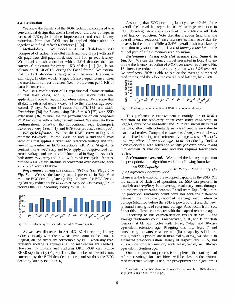
Performance during the nominal lifetime (i.e., Stage-0 in Fig. 7). We use the latency model presented in Eqn. 6 to estimate ECC decoding latency. Fig. 12 shows the ECC decod-ing latency reduction for ROR over baseline. On average, ROR reduces the ECC decoding latency by 10.1%.
Fig. 12. ECC decoding latency reduction of ROR over baseline.
As we have discussed in Sec. 4.3, BCH decoding latency reduces linearly with the raw bit error count in the data. In Stage-0, all the errors are correctable by ECC when any read reference voltage is applied (i.e., no read-retries are needed). However, by finding and applying OPT, ROR can reduce RBER significantly (Fig. 6). Thus, the number of raw bit errors corrected by the BCH decoder reduces, and so does the ECC decoding latency (see Eqn. 6).
Assuming that ECC decoding latency takes ~24% of the overall flash read latency, 8 the 10.1% average reduction in ECC decoding latency is equivalent to a 2.4% overall flash read latency reduction. Note that this fraction (and thus the overall latency reduction) may increase as flash page size in-creases in the future. While a 2.4% overall flash read latency reduction may sound small, it is a real latency reduction on the critical path of a flash memory read operation.
Performance during extended lifetime (i.e., Stage-1 in Fig. 7). We use the latency model presented in Eqn. 4 to es-timate the latency reduction of ROR over naive read-retry. Fig. 13 shows the reduction in read-retry count with ROR over na-ive read-retry. ROR is able to reduce the average number of read-retries, and therefore the overall read latency, by 70.4%.
Fig. 13. Read-retry count reduction of ROR over naive read-retry.
This performance improvement is mainly due to ROR’s reduction of the read-retry count over naive read-retry. In Stage-1, only naive read-retry and ROR can successfully read the data, albeit with potentially increased read latency due to extra read-retries. Compared to naive read-retry, which always uses a fixed starting read reference voltage across all blocks and regardless of retention age, ROR periodically finds a close-to-optimal read reference voltage for each block taking into account its retention age, and thus requires fewer read-retries.
Performance overhead. We model the latency to perform the pre-optimization algorithm with the following formula:
yReadLatencAvgRetryockPagesPerBlPageSizeβ
ySSDCapacitα
(7)
where α is the fraction of the occupied capacity in the SSD; β is the number of flash read operations the SSD can perform in parallel; and AvgRetry is the average read-retry count through-out the pre-optimization process. Recall from Eqn. 5 that, dur-ing power-on, read-retry count correlates with the difference between the previously-recorded starting read reference voltage (obtained before the SSD is powered off) and the new-ly-found starting read reference voltage. Also recall from Sec. 3 that this difference correlates with the elapsed retention age.
According to our characterization results in Sec. 3, the average ready-retry count is respectively 2, 10, and 15 for flash memory at 8k P/E cycles with 1-day, 7-day, and 30-day-equivalent retention age. Plugging this into Eqn. 7 and considering the worst-case scenario (flash capacity is full, i.e., α is 1, which is pessimistic in most real systems), we obtain an estimated pre-optimization latency of respectively 3, 15, and 23 seconds for flash memory with 1-day, 7-day, and 30-day-equivalent retention age.
Once the power-on process is completed, the starting read reference voltage for each block will be close to the optimal read reference voltage. Then, the pre-optimization algorithm is
8 We estimate the ECC decoding latency for a conventional BCH decoder
as (4 μs/8 Kbit) × 8 KB = 32 μs [28].
10
triggered daily to ensure the starting read reference voltages to catch up with the shifting of the threshold voltage distribution due to flash retention. As such, the flash controller can minimize read-retry count by reusing the previously-recorded read reference voltages. In this case, the latency for the pre-optimization algorithm is as low as 3 seconds, which can be largely hidden by executing the algorithm only when the SSD is idle or in the background at a lower priority.
Storage Overhead. We store the starting read reference voltages learned by ROR at a flash block granularity, leverag-ing our Observations 3 and 4 (Sec. 4.1). This greatly reduces the overhead compared to the alternative of recording the voltage at a page granularity. As a result, for our evaluated NAND flash device, the total storage overhead is 768 KB.9 This allows the flash controller to manage the ROR read reference voltage table completely within its DRAM buffer.
Summary. We conclude that our ROR technique is able to improve the P/E-cycle lifetime as well as the read performance of flash memory with only moderate latency overhead during the pre-optimization process and modest storage and logic overheads in the SSD controller.
5. Retention Failure Recovery (RFR)
In this section, we introduce another technique, Retention Failure Recovery (RFR), that allows us to recover data from flash memory offline after an ECC-uncorrectable retention failure happens (i.e., when the flash controller fails to read some data due to the inability to correct retention errors). We show in Sec. 5.1, that data loss, resulting from retention failure under various circumstances, can happen. In Sec. 5.2, we study the charge-leakage property of a flash memory cell, and de-scribe a technique to classify fast- and slow-leaking cells. This classification method enables the RFR technique, which we describe in Sec. 5.3, to recover an otherwise-uncorrectable retention error. In Sec. 5.4, we evaluate the raw bit error rate reduction benefit of the RFR technique.
5.1. Motivation for Offline Retention Error Recovery
The RFR technique is motivated by two major shortcom-ings of previously proposed flash refresh techniques [3][4][13][14]. First, these refresh techniques require the sys-tem to be consistently powered on; otherwise, uncorrectable errors may occur, resulting in data loss. Some use cases of flash memory, such as those in removable media and mobile devices, do not satisfy this requirement as these devices are not always powered-on. Even some always-on use cases of flash memory, such as those in some enterprise environments, may not always satisfy this requirement, as they may not always have an uninterrupted power supply to keep the SSDs pow-ered-on with zero downtime.
Second, the refresh period needs to be maintained conser-vatively (i.e., in a way that guarantees error correction with a
9 We store one byte per block for each starting read reference voltage
learned for the erased-P1 OPT, the P1-P2 OPT, and the P2-P3 OPT, which together consume a storage overhead of 3 B * 218 blocks = 768 KB. Note that
it is possible to further reduce this overhead by grouping flash blocks with
similar retention ages and storing a single set of read reference voltages for them or by storing only those read reference voltages that cause the most
retention errors (e.g., leveraging the observation in Finding 5 that retention
loss may affect the P2-P3 OPT much more significantly).
certain margin) by the flash controller to avoid unexpected data loss. However, this is difficult to guarantee in cases where temperature of flash memory increases very quickly. Increased temperature exponentially increases retention loss due to in-creased leakage and therefore increases the effective retention age of a flash memory block (i.e., the equivalent retention age of the block under room temperature10). This phenomenon can be modeled by Arrhenius Law [22]:
)/1/1()/(exp/ 2121 TTkEttAF a (8)
In Eqn. 8, AF is the aging factor, which is defined as the ra-tio between the effective retention age t1 under temperature T1 and the effective retention age t2 under temperature T2; Ea is the activation energy, which is a process-dependent constant, and k is the Boltzmann constant.
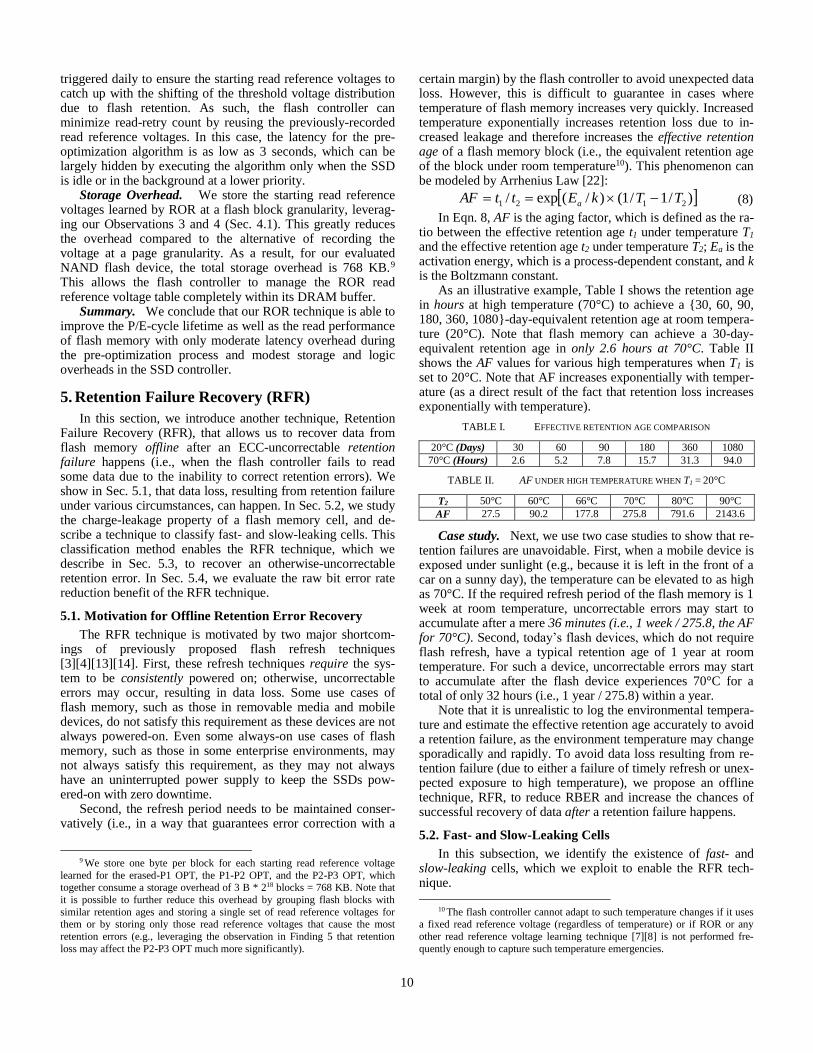
As an illustrative example, Table I shows the retention age in hours at high temperature (70°C) to achieve a {30, 60, 90, 180, 360, 1080}-day-equivalent retention age at room tempera-ture (20°C). Note that flash memory can achieve a 30-day-equivalent retention age in only 2.6 hours at 70°C. Table II shows the AF values for various high temperatures when T1 is set to 20°C. Note that AF increases exponentially with temper-ature (as a direct result of the fact that retention loss increases exponentially with temperature).
TABLE I. EFFECTIVE RETENTION AGE COMPARISON
20°C (Days) 30 60 90 180 360 1080
70°C (Hours) 2.6 5.2 7.8 15.7 31.3 94.0
TABLE II. AF UNDER HIGH TEMPERATURE WHEN T1 = 20°C
T2 50°C 60°C 66°C 70°C 80°C 90°C
AF 27.5 90.2 177.8 275.8 791.6 2143.6
Case study. Next, we use two case studies to show that re-tention failures are unavoidable. First, when a mobile device is exposed under sunlight (e.g., because it is left in the front of a car on a sunny day), the temperature can be elevated to as high as 70°C. If the required refresh period of the flash memory is 1 week at room temperature, uncorrectable errors may start to accumulate after a mere 36 minutes (i.e., 1 week / 275.8, the AF for 70°C). Second, today’s flash devices, which do not require flash refresh, have a typical retention age of 1 year at room temperature. For such a device, uncorrectable errors may start to accumulate after the flash device experiences 70°C for a total of only 32 hours (i.e., 1 year / 275.8) within a year.
Note that it is unrealistic to log the environmental tempera-ture and estimate the effective retention age accurately to avoid a retention failure, as the environment temperature may change sporadically and rapidly. To avoid data loss resulting from re-tention failure (due to either a failure of timely refresh or unex-pected exposure to high temperature), we propose an offline technique, RFR, to reduce RBER and increase the chances of successful recovery of data after a retention failure happens.
5.2. Fast- and Slow-Leaking Cells
In this subsection, we identify the existence of fast- and slow-leaking cells, which we exploit to enable the RFR tech-nique.
10 The flash controller cannot adapt to such temperature changes if it uses
a fixed read reference voltage (regardless of temperature) or if ROR or any
other read reference voltage learning technique [7][8] is not performed fre-
quently enough to capture such temperature emergencies.
11
At low retention age, the threshold voltage distributions of two neighboring states are far away from each other (Sec. 3.2). Hence, the data is likely to be read with a low and correctable error rate as long as a close-to-optimal read reference voltage is applied (Sec. 3.4). However, at a high retention age, the neigh-boring threshold voltage distributions become flatter and closer to each other (Sec. 3.2), and thus retention error count increas-es and a retention failure can appear. Also, recall from Finding 3 that the threshold voltage distribution shifts faster in higher-voltage states, such as P2 and P3. As a result, retention errors are more likely to happen in cells that are between the P2 and P3 states (i.e., in MSB pages). We use the P2 and P3 states as an example to illustrate our new findings.
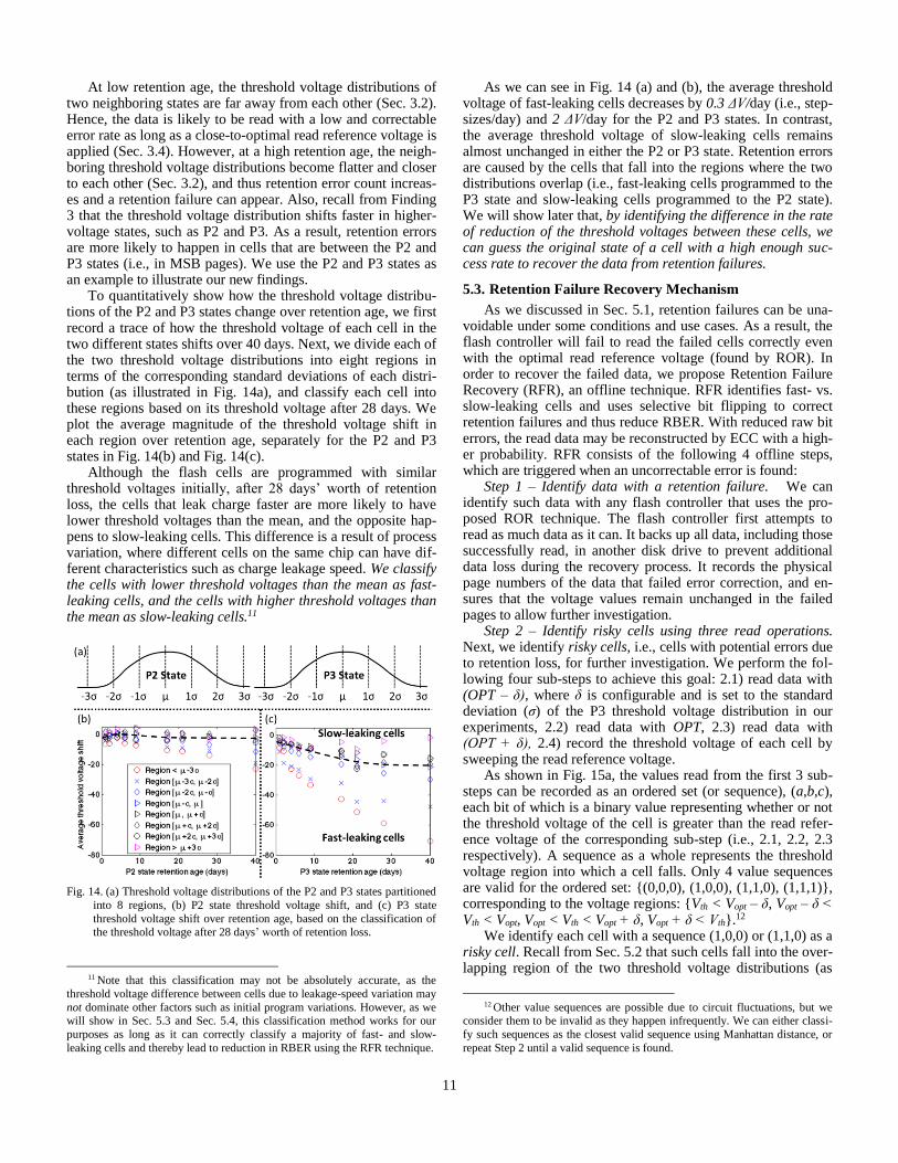
To quantitatively show how the threshold voltage distribu-tions of the P2 and P3 states change over retention age, we first record a trace of how the threshold voltage of each cell in the two different states shifts over 40 days. Next, we divide each of the two threshold voltage distributions into eight regions in terms of the corresponding standard deviations of each distri-bution (as illustrated in Fig. 14a), and classify each cell into these regions based on its threshold voltage after 28 days. We plot the average magnitude of the threshold voltage shift in each region over retention age, separately for the P2 and P3 states in Fig. 14(b) and Fig. 14(c).
Although the flash cells are programmed with similar threshold voltages initially, after 28 days’ worth of retention loss, the cells that leak charge faster are more likely to have lower threshold voltages than the mean, and the opposite hap-pens to slow-leaking cells. This difference is a result of process variation, where different cells on the same chip can have dif-ferent characteristics such as charge leakage speed. We classify the cells with lower threshold voltages than the mean as fast-leaking cells, and the cells with higher threshold voltages than the mean as slow-leaking cells.11
Fig. 14. (a) Threshold voltage distributions of the P2 and P3 states partitioned
into 8 regions, (b) P2 state threshold voltage shift, and (c) P3 state
threshold voltage shift over retention age, based on the classification of the threshold voltage after 28 days’ worth of retention loss.
11 Note that this classification may not be absolutely accurate, as the
threshold voltage difference between cells due to leakage-speed variation may
not dominate other factors such as initial program variations. However, as we will show in Sec. 5.3 and Sec. 5.4, this classification method works for our
purposes as long as it can correctly classify a majority of fast- and slow-
leaking cells and thereby lead to reduction in RBER using the RFR technique.
As we can see in Fig. 14 (a) and (b), the average threshold voltage of fast-leaking cells decreases by 0.3 ΔV/day (i.e., step-sizes/day) and 2 ΔV/day for the P2 and P3 states. In contrast, the average threshold voltage of slow-leaking cells remains almost unchanged in either the P2 or P3 state. Retention errors are caused by the cells that fall into the regions where the two distributions overlap (i.e., fast-leaking cells programmed to the P3 state and slow-leaking cells programmed to the P2 state). We will show later that, by identifying the difference in the rate of reduction of the threshold voltages between these cells, we can guess the original state of a cell with a high enough suc-cess rate to recover the data from retention failures.
5.3. Retention Failure Recovery Mechanism
As we discussed in Sec. 5.1, retention failures can be una-voidable under some conditions and use cases. As a result, the flash controller will fail to read the failed cells correctly even with the optimal read reference voltage (found by ROR). In order to recover the failed data, we propose Retention Failure Recovery (RFR), an offline technique. RFR identifies fast- vs. slow-leaking cells and uses selective bit flipping to correct retention failures and thus reduce RBER. With reduced raw bit errors, the read data may be reconstructed by ECC with a high-er probability. RFR consists of the following 4 offline steps, which are triggered when an uncorrectable error is found:
Step 1 – Identify data with a retention failure. We can identify such data with any flash controller that uses the pro-posed ROR technique. The flash controller first attempts to read as much data as it can. It backs up all data, including those successfully read, in another disk drive to prevent additional data loss during the recovery process. It records the physical page numbers of the data that failed error correction, and en-sures that the voltage values remain unchanged in the failed pages to allow further investigation.
Step 2 – Identify risky cells using three read operations. Next, we identify risky cells, i.e., cells with potential errors due to retention loss, for further investigation. We perform the fol-lowing four sub-steps to achieve this goal: 2.1) read data with (OPT – δ), where δ is configurable and is set to the standard deviation (σ) of the P3 threshold voltage distribution in our experiments, 2.2) read data with OPT, 2.3) read data with (OPT + δ), 2.4) record the threshold voltage of each cell by sweeping the read reference voltage.
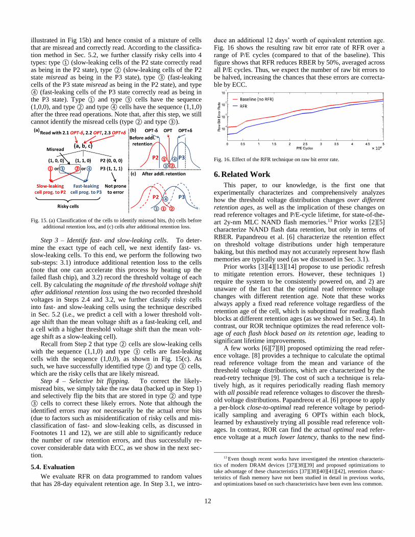
As shown in Fig. 15a, the values read from the first 3 sub-steps can be recorded as an ordered set (or sequence), (a,b,c), each bit of which is a binary value representing whether or not the threshold voltage of the cell is greater than the read refer-ence voltage of the corresponding sub-step (i.e., 2.1, 2.2, 2.3 respectively). A sequence as a whole represents the threshold voltage region into which a cell falls. Only 4 value sequences are valid for the ordered set: {(0,0,0), (1,0,0), (1,1,0), (1,1,1)}, corresponding to the voltage regions: {Vth < Vopt – δ, Vopt – δ < Vth < Vopt, Vopt < Vth < Vopt + δ, Vopt + δ < Vth}.12
We identify each cell with a sequence (1,0,0) or (1,1,0) as a risky cell. Recall from Sec. 5.2 that such cells fall into the over-lapping region of the two threshold voltage distributions (as
12 Other value sequences are possible due to circuit fluctuations, but we
consider them to be invalid as they happen infrequently. We can either classi-
fy such sequences as the closest valid sequence using Manhattan distance, or
repeat Step 2 until a valid sequence is found.
12
illustrated in Fig 15b) and hence consist of a mixture of cells that are misread and correctly read. According to the classifica-tion method in Sec. 5.2, we further classify risky cells into 4 types: type ① (slow-leaking cells of the P2 state correctly read as being in the P2 state), type ② (slow-leaking cells of the P2 state misread as being in the P3 state), type ③ (fast-leaking cells of the P3 state misread as being in the P2 state), and type ④ (fast-leaking cells of the P3 state correctly read as being in the P3 state). Type ① and type ③ cells have the sequence (1,0,0), and type ② and type ④ cells have the sequence (1,1,0) after the three read operations. Note that, after this step, we still cannot identify the misread cells (type ② and type ③).
Fig. 15. (a) Classification of the cells to identify misread bits, (b) cells before
additional retention loss, and (c) cells after additional retention loss.
Step 3 – Identify fast- and slow-leaking cells. To deter-mine the exact type of each cell, we next identify fast- vs. slow-leaking cells. To this end, we perform the following two sub-steps: 3.1) introduce additional retention loss to the cells (note that one can accelerate this process by heating up the failed flash chip), and 3.2) record the threshold voltage of each cell. By calculating the magnitude of the threshold voltage shift after additional retention loss using the two recorded threshold voltages in Steps 2.4 and 3.2, we further classify risky cells into fast- and slow-leaking cells using the technique described in Sec. 5.2 (i.e., we predict a cell with a lower threshold volt-age shift than the mean voltage shift as a fast-leaking cell, and a cell with a higher threshold voltage shift than the mean volt-age shift as a slow-leaking cell).
Recall from Step 2 that type ② cells are slow-leaking cells with the sequence (1,1,0) and type ③ cells are fast-leaking cells with the sequence (1,0,0), as shown in Fig. 15(c). As such, we have successfully identified type ② and type ③ cells, which are the risky cells that are likely misread.
Step 4 – Selective bit flipping. To correct the likely-misread bits, we simply take the raw data (backed up in Step 1) and selectively flip the bits that are stored in type ② and type ③ cells to correct these likely errors. Note that although the identified errors may not necessarily be the actual error bits (due to factors such as misidentification of risky cells and mis-classification of fast- and slow-leaking cells, as discussed in Footnotes 11 and 12), we are still able to significantly reduce the number of raw retention errors, and thus successfully re-cover considerable data with ECC, as we show in the next sec-tion.
5.4. Evaluation
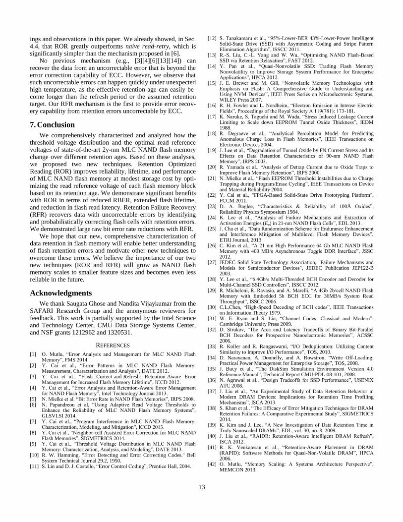
We evaluate RFR on data programmed to random values that has 28-day equivalent retention age. In Step 3.1, we intro-
duce an additional 12 days’ worth of equivalent retention age. Fig. 16 shows the resulting raw bit error rate of RFR over a range of P/E cycles (compared to that of the baseline). This figure shows that RFR reduces RBER by 50%, averaged across all P/E cycles. Thus, we expect the number of raw bit errors to be halved, increasing the chances that these errors are correcta-ble by ECC.
Fig. 16. Effect of the RFR technique on raw bit error rate.
6. Related Work
This paper, to our knowledge, is the first one that experimentally characterizes and comprehensively analyzes how the threshold voltage distribution changes over different retention ages, as well as the implication of these changes on read reference voltages and P/E-cycle lifetime, for state-of-the-art 2y-nm MLC NAND flash memories.13 Prior works [2][5] characterize NAND flash data retention, but only in terms of RBER. Papandreou et al. [6] characterize the retention effect on threshold voltage distributions under high temperature baking, but this method may not accurately represent how flash memories are typically used (as we discussed in Sec. 3.1).
Prior works [3][4][13][14] propose to use periodic refresh to mitigate retention errors. However, these techniques 1) require the system to be consistently powered on, and 2) are unaware of the fact that the optimal read reference voltage changes with different retention age. Note that these works always apply a fixed read reference voltage regardless of the retention age of the cell, which is suboptimal for reading flash blocks at different retention ages (as we showed in Sec. 3.4). In contrast, our ROR technique optimizes the read reference volt-age of each flash block based on its retention age, leading to significant lifetime improvements.
A few works [6][7][8] proposed optimizing the read refer-ence voltage. [8] provides a technique to calculate the optimal read reference voltage from the mean and variance of the threshold voltage distributions, which are characterized by the read-retry technique [9]. The cost of such a technique is rela-tively high, as it requires periodically reading flash memory with all possible read reference voltages to discover the thresh-old voltage distributions. Papandreou et al. [6] propose to apply a per-block close-to-optimal read reference voltage by period-ically sampling and averaging 6 OPTs within each block, learned by exhaustively trying all possible read reference volt-ages. In contrast, ROR can find the actual optimal read refer-ence voltage at a much lower latency, thanks to the new find-
13 Even though recent works have investigated the retention characteris-
tics of modern DRAM devices [37][38][39] and proposed optimizations to take advantage of these characteristics [37][38][40][41][42], retention charac-
teristics of flash memory have not been studied in detail in previous works,
and optimizations based on such characteristics have been even less common.
13
ings and observations in this paper. We already showed, in Sec. 4.4, that ROR greatly outperforms naive read-retry, which is significantly simpler than the mechanism proposed in [6].
No previous mechanism (e.g., [3][4][6][13][14]) can recover the data from an uncorrectable error that is beyond the error correction capability of ECC. However, we observe that such uncorrectable errors can happen quickly under unexpected high temperature, as the effective retention age can easily be-come longer than the refresh period or the assumed retention target. Our RFR mechanism is the first to provide error recov-ery capability from retention errors uncorrectable by ECC.
7. Conclusion
We comprehensively characterized and analyzed how the threshold voltage distribution and the optimal read reference voltages of state-of-the-art 2y-nm MLC NAND flash memory change over different retention ages. Based on these analyses, we proposed two new techniques. Retention Optimized Reading (ROR) improves reliability, lifetime, and performance of MLC NAND flash memory at modest storage cost by opti-mizing the read reference voltage of each flash memory block based on its retention age. We demonstrate significant benefits with ROR in terms of reduced RBER, extended flash lifetime, and reduction in flash read latency. Retention Failure Recovery (RFR) recovers data with uncorrectable errors by identifying and probabilistically correcting flash cells with retention errors. We demonstrated large raw bit error rate reductions with RFR.
We hope that our new, comprehensive characterization of data retention in flash memory will enable better understanding of flash retention errors and motivate other new techniques to overcome these errors. We believe the importance of our two new techniques (ROR and RFR) will grow as NAND flash memory scales to smaller feature sizes and becomes even less reliable in the future.
Acknowledgments
We thank Saugata Ghose and Nandita Vijaykumar from the SAFARI Research Group and the anonymous reviewers for feedback. This work is partially supported by the Intel Science and Technology Center, CMU Data Storage Systems Center, and NSF grants 1212962 and 1320531.
REFERENCES
[1] O. Mutlu, “Error Analysis and Management for MLC NAND Flash Memory”, FMS 2014.
[2] Y. Cai et al., “Error Patterns in MLC NAND Flash Memory: Measurement, Characterization and Analysis”, DATE 2012.
[3] Y. Cai et al., “Flash Correct-and-Refresh: Retention-Aware Error Management for Increased Flash Memory Lifetime”, ICCD 2012.
[4] Y. Cai et al., “Error Analysis and Retention-Aware Error Management for NAND Flash Memory”, Intel Technology Journal 2013.
[5] N. Mielke et al. “Bit Error Rate in NAND Flash Memories”, IRPS 2008. [6] N. Papandreou et al, “Using Adaptive Read Voltage Thresholds to
Enhance the Reliability of MLC NAND Flash Memory Systems”, GLSVLSI 2014.
[7] Y. Cai et al., “Program Interference in MLC NAND Flash Memory: Characterization, Modeling, and Mitigation”, ICCD 2013.
[8] Y. Cai et al., “Neighbor-cell Assisted Error Correction for MLC NAND Flash Memories”, SIGMETRICS 2014.
[9] Y. Cai et al., “Threshold Voltage Distribution in MLC NAND Flash Memory: Characterization, Analysis, and Modeling”, DATE 2013.
[10] R. W. Hamming, "Error Detecting and Error Correcting Codes." Bell System Technical Journal 29.2, 1950.
[11] S. Lin and D. J. Costello, “Error Control Coding”, Prentice Hall, 2004.
[12] S. Tanakamaru et al., “95%-Lower-BER 43%-Lower-Power Intelligent Solid-State Drive (SSD) with Asymmetric Coding and Stripe Pattern Elimination Algorithm”, ISSCC 2011.
[13] R.-S. Liu, C.-L. Yang and W. Wu, “Optimizing NAND Flash-Based SSD via Retention Relaxation”, FAST 2012.
[14] Y. Pan et al., “Quasi-Nonvolatile SSD: Trading Flash Memory Nonvolatility to Improve Storage System Performance for Enterprise Applications”, HPCA 2012.
[15] J. E. Brewer and M. Gill, “Nonvolatile Memory Technologies with Emphasis on Flash: A Comprehensive Guide to Understanding and Using NVM Devices”, IEEE Press Series on Microelectronic Systems, WILEY Press 2007.
[16] R. H. Fowler and L. Nordheim, “Electron Emission in Intense Electric Fields”, Proceedings of the Royal Society A 119(781): 173-181.
[17] K. Naruke, S. Taguchi and M. Wada, “Stress Induced Leakage Current Limiting to Scale down EEPROM Tunnel Oxide Thickness”, IEDM 1988.
[18] R. Degraeve et al., “Analytical Percolation Model for Predicting Anomalous Charge Loss in Flash Memories”, IEEE Transactions on Electronic Devices 2004.
[19] J. Lee et al., “Degradation of Tunnel Oxide by FN Current Stress and Its Effects on Data Retention Characteristics of 90-nm NAND Flash Memory”, IRPS 2003.
[20] R. Yamada et al., “Analysis of Detrap Current due to Oxide Traps to Improve Flash Memory Retention”, IRPS 2000.
[21] N. Mielke et al., “Flash EEPROM Threshold Instabilities due to Charge Trapping during Program/Erase Cycling”, IEEE Transactions on Device and Material Reliability 2004.
[22] Y. Cai et al., "FPGA-Based Solid-State Drive Prototyping Platform", FCCM 2011.
[23] D. A. Baglee, “Characteristics & Reliability of 100Å Oxides”, Reliability Physics Symposium 1984.
[24] K. Lee et al., “Analysis of Failure Mechanisms and Extraction of Activation Energies (Ea) in 21-nm NAND Flash Cells”, EDL 2013.
[25] J. Cha et al., “Data Randomization Scheme for Endurance Enhancement and Interference Mitigation of Multilevel Flash Memory Devices”, ETRI Journal, 2013.
[26] C. Kim et al., “A 21 nm High Performance 64 Gb MLC NAND Flash Memory with 400 MB/s Asynchronous Toggle DDR Interface”, JSSC 2012.
[27] JEDEC Solid State Technology Association, "Failure Mechanisms and Models for Semiconductor Devices", JEDEC Publication JEP122-B 2003.
[28] Y. Lee et al., “6.4Gb/s Multi-Threaded BCH Encoder and Decoder for Multi-Channel SSD Controllers”, ISSCC 2012.
[29] R. Micheloni, R. Ravasio, and A. Marelli, “A 4Gb 2b/cell NAND Flash Memory with Embedded 5b BCH ECC for 36MB/s System Read Throughput”, ISSCC 2006.
[30] C.L.Chen, “High-Speed Decoding of BCH codes”, IEEE Transactions on Information Theory 1979.
[31] W. E. Ryan and S. Lin, “Channel Codes: Classical and Modern”, Cambridge University Press 2009.
[32] D. Strukov, “The Area and Latency Tradeoffs of Binary Bit-Parallel BCH Decoders for Prospective Nanoelectronic Memories”, ACSSC 2006.
[33] R. Koller and R. Rangaswami, “I/O Deduplication: Utilizing Content Similarity to Improve I/O Performance”, TOS, 2010.
[34] D. Narayanan, A. Donnelly, and A. Rowstron, “Write Off-Loading: Practical Power Management for Enterprise Storage”, TOS, 2008.
[35] J. Bucy et al., “The DiskSim Simulation Environment Version 4.0 Reference Manual”, Technical Report CMU-PDL-08-101, 2008.
[36] N. Agrawal et al., “Design Tradeoffs for SSD Performance”, USENIX ATC 2008.
[37] J. Liu et al., “An Experimental Study of Data Retention Behavior in Modern DRAM Devices: Implications for Retention Time Profiling Mechanisms”, ISCA 2013.
[38] S. Khan et al., “The Efficacy of Error Mitigation Techniques for DRAM Retention Failures: A Comparative Experimental Study”, SIGMETRICS 2014.
[39] K. Kim and J. Lee, “A New Investigation of Data Retention Time in Truly Nanoscaled DRAMs”, EDL, vol. 30, no. 8, 2009.
[40] J. Liu et al., “RAIDR: Retention-Aware Intelligent DRAM Refresh”, ISCA 2012.
[41] R. K. Venkatesan et al., “Retention-Aware Placement in DRAM (RAPID): Software Methods for Quasi-Non-Volatile DRAM”, HPCA 2006.
[42] O. Mutlu, “Memory Scaling: A Systems Architecture Perspective”, MEMCON 2013.