escapee - tayloredge
TRANSCRIPT

SiC Workshop. EPE 2005, September 12 ESCAPEE Project
1
ESCAPEE
EPE 2005 DresdenEPE 2005 Dresden

SiC Workshop. EPE 2005, September 12 ESCAPEE Project
2
The achievements of the EC funded project "EstablishSilicon Carbide Applications for Power Electronics in
Europe" (ESCAPEE)
J. Millan1, P. Godignon1, D. Tournier1, P.A. Mawby2, S. Wilks2, O.J. Guy2,and L. Chen2, R. Bassett3, A. Hyde3, N. Martin4, M. Mermet-Guyennet4, S.Pasugcio4, S. P M. Syväjärvi5, R.R. Ciechonski5, R. Yakimova5, L. Roux6,
F. Torregrosa6, T. Bouchet6, J-M. Bluet7, G. Guillot7, D. Hinchley8, S.Jones8, J. Rhodes8, P. Taylor9 and P. Waind9
1Centro Nacional de Microelectrónica, Campus Universidad Autónoma deBarcelona, 2School of Engineering, University of Wales Swansea,
3ALSTOM Research & Technology Centre, 4ALSTOM Transport SA,5Department of Physics and Measurement Technology, Linköping
University, Sweden, 6Ion Beam Services, 7Institut National des SciencesAppliquées de Lyon, Laboratoire de Physique de la Matiere CNRS,
8Semelab Plc, 9Dynex Semiconductor Ltd.

SiC Workshop. EPE 2005, September 12 ESCAPEE Project
3
Overview
• Overview of recent results from the ESCAPEE project.• Update to the information originally presented at EPE 2003 in
Toulouse.• Key targets• Significant scientific progresses• Final achievements and successes.
SiC Workshop. EPE 2005, September 12 ESCAPEE Project
4
Key research targets(creation and introduction of SiC technology, from fundamentalscience through to real applications.)
• Produce improved quality of thick (>10μm) SiC epi-layermaterial suitable for high power devices.
• Develop device processing and fabrication technology(implantation, passivation, etching, metallization).
• Establish edge termination to enable high voltage applications.• Develop high temperature device packaging suitable for SiC• Use the created technology in a module introduction and end-
user application in traction systems

SiC Workshop. EPE 2005, September 12 ESCAPEE Project
5
Important scientific progressesSignificant results from the ESCAPEE project include:
• Development of new sublimation epitaxial growth technique - produces epi-layers at growth rates up to 20 times faster than standard CVD growth.
• Development of high temperature implantation equipment for SiC and thesubsequent commercialisation.
• Development of surface cleaning processes and reduction of surfacedamage produced by high temperature annealing, for implant activation.
• Development of low resistance n-type and p-type ohmic contacts and highquality Schottky diodes.
• Design of edge termination and fabrication of thermally stable Schottkydiodes with blocking voltages of up to 4.7kV and reverse leakage currentsof less than 2e-7 A/cm2 at 3.5kV.
• Increased device yield of 1.6mm ×1.6mm diodes from 12% to 43% using anovel polishing technique.

SiC Workshop. EPE 2005, September 12 ESCAPEE Project
6
Significant results from the ESCAPEE project continued…
• Development of 1.2 kV MOSFETs.
• Record Field-effect mobility and drain current as a function of gatevoltage for transistors with a PVT grown epilayer and a reference CVDgrown epilayer.
• Design and production of specialized high temperature thermally stablepackaging for high voltage SiC devices.
• Production of a demonstrator module using SiC diodes and Si IGBTs.

SiC Workshop. EPE 2005, September 12 ESCAPEE Project
7
ESCAPEE Technological developments

SiC Workshop. EPE 2005, September 12 ESCAPEE Project
8
•Sublimation of a solid source and transport of vapor to a substrate•ideas based on the sublimation growth process to produce wafers butsmaller distance between source and substrate
•Benefit of high growth rate from intrinsic sublimation to yield thick layers
•Develop growth conditions to achieve smooth surfaces and low doping
Fast epitaxy by PVT
ESCAPEE’s results – Material

SiC Workshop. EPE 2005, September 12 ESCAPEE Project
9
0
0,01
0,02
0,03
0,04
0
50
100
150
200
250
-5 0 5 10 15 20 25 30Gate voltage [V]
PVT
CVD
tox
= 1550 Å,
L = 20 μm, W= 100 μm
CVD, ID
PVT, ID
• Low doping in the E15 range has beenachieved
• Causes for the background doping areknown and even lower doping isexpected
• Higher field-effect mobility and draincurrent for transistors with a PVT grownepilayer than on reference CVD grownepilayer.
• A patent on the fast PVT epitaxytechnology has been filed
• Discussions with partners forcommercialization are in progress
Achievements

SiC Workshop. EPE 2005, September 12 ESCAPEE Project
10
ESCAPEE’s results – Implantation
High temperature implanterHigh temp chucks : - Several versions available and already sold (Univ. Madrid, INRS Canada, LETI.)
V2 : Installed in Madrid Proto of V3 : Installed at INRS (Canada)

SiC Workshop. EPE 2005, September 12 ESCAPEE Project
11
• Results using Graphite cap – surface protection process arepromising.
SiC
Photoresist
SiC
Carbon
SiC
RIE
750°C Anneal (Ar)
• Carbon cap produced by annealing photoresistunder argon (750°C)
• Anneal sample as before (1600° for 30 min)
• Remove Carbon Cap (RIE with O2)
Novel process technological step

SiC Workshop. EPE 2005, September 12 ESCAPEE Project
12
Carbon cap experiment
Surface roughness reduced by up to a factor of 10Improved forward I(V) characteristicsImproved reverse leakage currents
(a) (b)
C-cap protectedNot protected

SiC Workshop. EPE 2005, September 12 ESCAPEE Project
13
1.2 kV SCHOTTKY DIODES

SiC Workshop. EPE 2005, September 12 ESCAPEE Project
14
1.2 kV Schottky Diodes – Area dependence and wafer uniformity
Forward mode I(V) curves at 350ºC for various device area
I(V) uniformity: Thickness and doping OK
0,0 0,5 1,0 1,5 2,0 2,5 3,0 3,5 4,00,00
0,25
0,50
0,75
1,00
0.4 x 0.4 mm2
0.8 x 0.8 mm2
1.6 x 1.6 mm2
0,0 0,5 1,0 1,5 2,0 2,5 3,0 3,5 4,01E-8
1E-7
1E-6
1E-5
1E-4
1E-3
0,01
0,1
1
For
war
d cu
rren
t (A
)
Forward voltage (V)
ESC12 - AsDep
Forw
ard
curr
ent (
A)
Forward voltage (V)ESC12 - AsDep

SiC Workshop. EPE 2005, September 12 ESCAPEE Project
15
Manufacturing yield versus Chip size and wafermicropipes density
0,5 1,0 1,5 2,0 2,540
50
60
70
80
90
100
Chip size (mm x mm)
Yiel
d (%
) = e
xp (A
rea
* D)
1/cm2
5/cm2
2/cm2
16/cm2
30/cm2
Unpolished Polished ESC12_UnPolished
1.2 kV SCHOTTKY DIODES - Yield
Escapee samples
Escapee samples
Escapee samples

SiC Workshop. EPE 2005, September 12 ESCAPEE Project
16
Discrete Package
• New package uses DBC baseplate,eliminating separate copperbaseplate and DBC substrate used inthe conventional isolated TO-257.
• Offers reduction in weight, improvedreliability and the potential to operateat elevated temperatures.
• Package successfully used tocharacterise 1000V ESCAPEEdiodes at 225°C.
• Limited VR to 800V during hot test toavoid destroying devices.
DBC TO-257 Package

SiC Workshop. EPE 2005, September 12 ESCAPEE Project
17
Diode Characterisation
Packaged devices show little area dependence and better stability andduring device testing
Diode Forward Characteristics Diode Reverse Characteristics

SiC Workshop. EPE 2005, September 12 ESCAPEE Project
18
High-Temperature Operation
0
2
4
6
8
10
12
0 1 2 3 4 5VF (V)
IF (A
)
25°C125°C225°C
1E-06
1E-05
1E-04
1E-03
1E-02
25 75 125 175 225TJ (°C)
IR (A
)
Diode Reverse Characteristics (at 800V)Diode Forward Characteristics

SiC Workshop. EPE 2005, September 12 ESCAPEE Project
19
Temperature dependence on the dynamic behavior
of the 2.16 mm2 SiC SBD
1.2 kV SCHOTTKY DIODES – switching T dependence
No significant impact of temperature on switchingcharacteristics

SiC Workshop. EPE 2005, September 12 ESCAPEE Project
20
ESCAPEE’s resultsCompact modelling
-4
-2
0
2
4
6
8
0.0E+00 5.0E-08 1.0E-07 1.5E-07 2.0E-07 2.5E-07
Time (s)I (
A)
Ultra-fast Si PiN diode
ESCAPEE SiC Schottky
ESCAPEE model
0.00E+00
5.00E+01
1.00E+02
1.50E+02
2.00E+02
2.50E+02
3.00E+02
0 0.5 1 1.5 2 2.5 3 3.5 4 4.5 5
Temperature (K)
J (A
/cm
2 )
SM d34 T=300K
SM d34 T=473
SM d34 T=573K
JA d34fb25
JA d34fb 473
JA d34fb 573
DC Switching

SiC Workshop. EPE 2005, September 12 ESCAPEE Project
21
1.2KV Hybrid Module
• Aerospace IGBT/diode half-bridge module.
• 150A 1200V Infineon SiliconIGBT.
• Four 1.6x1.6mm 1000VESCAPEE SiC Schottky Diodesin parallel.
• AlSiC Baseplate, Al/AlNsubstrate, Cu lead-frame, PBTring-frame and lid.
• PbSnAg solder and vacuumfurnace die-attach.
• 5mil/12 mil Al wire-bonds. Si IGBT/SiC diode hybridmodule with lid removed

SiC Workshop. EPE 2005, September 12 ESCAPEE Project
22
Hybrid Module Characterisation
• Three IGBT/diode substratesexhibited IR<300uA at 1000V.
• One IGBT/diode substratesuffered fractured breakdowncharacteristic above 600V.
• VF < 3V at 50A, 25°C.• Module successfully switched
25°C, 50A, 600V, 500A/us.
0
10
20
30
40
50
60
0 0.5 1 1.5 2 2.5 3VF (V)
IF (A
)
Hybrid Module SiC Diode ForwardCharacteristics

SiC Workshop. EPE 2005, September 12 ESCAPEE Project
23
ESCAPEE’s results
Si IGBT/SiC diode hybrid module inductive-loadswitching at 25°C, 50A, 600V, 500A/us.
Hybrid Module Switching

SiC Workshop. EPE 2005, September 12 ESCAPEE Project
24
3.5 kV SCHOTTKY DIODES

SiC Workshop. EPE 2005, September 12 ESCAPEE Project
25
Diodes fabrication for module• 4.5 kV ESCAPEE Schottky diodes fabricatedat CNM for hybrid module
• Good current density uniformity vs diodes size• RON= 40mΩ.cm2 close to theoretical expectedvalue (31mΩ.cm2).
• Ni used as Schottky contact - stabilitydemonstrated up to 200°C
•Very low reverse leakage current density(JR<10 µA/cm2 @ 3.5kV)
• No breakdown differences betweenmeasurements made in the air and insidegalden on polyimide passivated devices.
4.7kV Breakdown voltage measured =termination efficiency of at least 80%
0,0 0,5 1,0 1,5 2,0 2,5 3,00
10
20
30
40
50
RON = 40 mΩ.cm2
ΦB = 0,74ev Cur
rent
den
sity
(A/c
m2 )
Voltage (V)
0.4x0.4 0.8x0.8 1.2x1.2 1.6x1.6
Schottky diode forwardcharacteristics versus size.
-4000 -3000 -2000 -1000 01E-11
1E-10
1E-9
1E-8
1E-7
1E-6
1E-51,6 x 1,6 mm2
Rev
erse
Cur
rent
(A)
Reverse voltage (V)
Id
Schottky diode reverse characteristics

SiC Workshop. EPE 2005, September 12 ESCAPEE Project
26
4.5 kV- 8A Module fabrication
High voltage packagingtechnology successfully applied toSi/SiC hybrid module fabrication
• Power Modules have been constructedintegrating Si IGBTs and SiC Schottky diodesin chopper configuration
• High voltage 4.5 kV SiC diodes have beensuccessfully assembled with high-voltage SiIGBTs into modules and characterized byDynex Semiconductor.
3D-High voltagemodule CAD view.
Arm electrical equivalentcircuit, packaged diodes

SiC Workshop. EPE 2005, September 12 ESCAPEE Project
27
Module characterisation
• The measured on-resistance of thediode is lower and nearer to thetheoretical value when measured onpackaged devices.
• SiC Schottky diodes show excellentbehaviour in forward mode up to125ºC1 2 3 4 5 6
0
4
8
12
16
0
26
52
78
104
J F(A) (
per d
ie)
I F(A
) (m
odul
e)
VF(V)
IF (20ºC) IF (125ºC)
Schottky diode forward characteristics.Module I(V) left, Die J(V) right, at 20ºCand 125ºC

SiC Workshop. EPE 2005, September 12 ESCAPEE Project
28
Module characterisation
SiC Schottky diode leakage current levelcompatible with Si-IGBT
• very low leakage currentvalues have been measured at3.1kV (curve tracer limit) in thereverse mode.• diode arm leakage current(8µA @ 3.1kV) is in the samerange than that of the Si-IGBTarm.
Experimental SiC-Schottky diode and Si-IGBTmodules forward characteristics and reverseleakage current at 3.1kV reverse bias.
3µA8µ[email protected] kV, 20°C
26A/cm2@ VF=3V
Forward 125 °C
50A/cm2@ VF=3V
Forward 20 °C
IGBT armDiode arm
SiC Workshop. EPE 2005, September 12 ESCAPEE Project
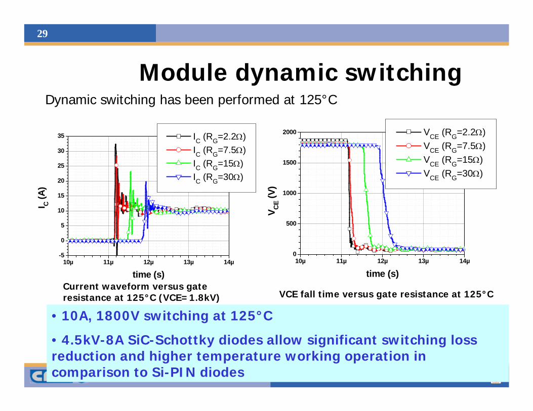
29
Module dynamic switchingDynamic switching has been performed at 125°C
10µ 11µ 12µ 13µ 14µ-5
0
5
10
15
20
25
30
35
I C (A
)
time (s)
IC (RG=2.2Ω) IC (RG=7.5Ω) IC (RG=15Ω) IC (RG=30Ω)
10µ 11µ 12µ 13µ 14µ0
500
1000
1500
2000
V CE
(V)
time (s)
VCE (RG=2.2Ω) VCE (RG=7.5Ω) VCE (RG=15Ω) VCE (RG=30Ω)
Current waveform versus gateresistance at 125°C (VCE=1.8kV) VCE fall time versus gate resistance at 125°C
• 10A, 1800V switching at 125°C
• 4.5kV-8A SiC-Schottky diodes allow significant switching lossreduction and higher temperature working operation incomparison to Si-PIN diodes

SiC Workshop. EPE 2005, September 12 ESCAPEE Project
30
Power MOSFET Fabrication

SiC Workshop. EPE 2005, September 12 ESCAPEE Project
31
Interface density state in the SiC gap near the conduction band
Gate oxide capacitances
0.15 0.20 0.25 0.30 0.35 0.40
1011
1012
1013
TEOS + RTA N2O
TEOS + N2
O2 + TEOS +O2
O2 + TEOS + Ar
100 nm TEOS
Inte
rfac
e D
ensi
ty S
tate
s [c
m-2eV
-1]
EC-ET [eV]
N2O + TEOS

SiC Workshop. EPE 2005, September 12 ESCAPEE Project
32
Lateral N-MOSFET test structureN-MOSFET on 4H-SiC: Thermal N2O /100nm TEOS / 950ºC O2
• Current higher than usual (x4 compared to LiU S230)• Threshold voltage: in the range –1V / 0.5V ( short/long channel)• Channel mobility: 40- 45 cm2/Vs (on epilayer layer annealed at 1600ºC)• Stable up to 15V
0 1 2 3 4 50,0
0,5
1,0
1,5
Vg=2V
Vg=4V
Vg=6V
Vg=8V
Dra
in C
urre
nt [m
A]
Drain-Source Bias [V]
Vg=10V
-4 -2 0 2 4 6 8 10 12 140
10
20
30
40
50
60
Thermal Oxide
Effe
ctiv
e M
obili
ty μ
eff [c
m2 /V
s]
Gate Bias [V]
N2O + TEOS
Channel mobility vs gate bias

SiC Workshop. EPE 2005, September 12 ESCAPEE Project
33
ESCAPEE CURRENT STATUS:
1.2 kV Schottky diodes process stable with good yield
3.5 kV Schottky diodes process repetitive: yield depends on wafer quality
Gate dielectric with channel mobility on implanted layer: 50 cm2/Vs
1.2 kV and 3.5 kV Power MOSFETs in processing

SiC Workshop. EPE 2005, September 12 ESCAPEE Project
34
Si/SiC hybride modulesSi/SiC hybride modules