energy-e–cient analog-to-digital conversion for ultra ... control logic, a new capacitive ......
TRANSCRIPT
Energy-Efficient Analog-to-Digital Conversion for
Ultra-Wideband Radio
by
Brian P. Ginsburg
Submitted to the Department of Electrical Engineering and ComputerScience
in partial fulfillment of the requirements for the degree of
Doctor of Philosophy
at the
MASSACHUSETTS INSTITUTE OF TECHNOLOGY
July 2007
c© Massachusetts Institute of Technology 2007. All rights reserved.
Author . . . . . . . . . . . . . . . . . . . . . . . . . . . . . . . . . . . . . . . . . . . . . . . . . . . . . . . . . . . . . . . . . . . .Department of Electrical Engineering and Computer Science
July 25, 2007
Certified by . . . . . . . . . . . . . . . . . . . . . . . . . . . . . . . . . . . . . . . . . . . . . . . . . . . . . . . . . . . . . . .Anantha P. Chandrakasan
Professor of Electrical Engineering and Computer ScienceThesis Supervisor
Accepted by . . . . . . . . . . . . . . . . . . . . . . . . . . . . . . . . . . . . . . . . . . . . . . . . . . . . . . . . . . . . . . .Arthur C. Smith
Chairman, Department Committee on Graduate Students

2

Energy-Efficient Analog-to-Digital Conversion for
Ultra-Wideband Radio
by
Brian P. Ginsburg
Submitted to the Department of Electrical Engineering and Computer Scienceon July 25, 2007, in partial fulfillment of the
requirements for the degree ofDoctor of Philosophy
Abstract
In energy constrained signal processing and communication systems, a focus on the analog ordigital circuits in isolation cannot achieve the minimum power consumption. Furthermore, inadvanced technologies with significant variation, yield is traditionally achieved only throughconservative design and a sacrifice of energy efficiency. In this thesis, these limitations areaddressed with both a comprehensive mixed-signal design methodology and new circuitsand architectures, as presented in the context of an analog-to-digital converter (ADC) forultra-wideband (UWB) radio.
UWB is an emerging technology capable of high-data-rate wireless communication andprecise locationing, and it requires high-speed (>500MS/s), low-resolution ADCs. Thesuccessive approximation register (SAR) topology exhibits significantly reduced complex-ity compared to the traditional flash architecture. Three time-interleaved SAR ADCs havebeen implemented. At the mixed-signal optimum energy point, parallelism and reduced volt-age supplies provide more than 3× energy savings. Custom control logic, a new capacitiveDAC, and a hierarchical sampling network enable the high-speed operation. Finally, only asmall amount of redundancy, with negligible power penalty, dramatically improves the yieldof the highly parallel ADC in deep sub-micron CMOS.
Thesis Supervisor: Anantha P. ChandrakasanTitle: Professor of Electrical Engineering and Computer Science
3

4

Acknowledgments
This thesis is the culmination of four years of dedicated study, and many have assisted and
encouraged me along the way, without whom this project and document would never have
gotten off the ground.
I would first like to thank my advisor, Professor Anantha Chandrakasan. He was my
undergraduate academic advisor, and I joined his research group because he offered me the
opportunity to define my own project directions. He has been incredibly supportive through-
out, keeping me on track with the big picture and tapeout and paper goals but allowing me
to continually evolve this project towards my final chip. His support was instrumental in
helping me, first, identify the problems that I wanted to solve and then going off to solve
them. Anantha has such a prominent presence throughout the circuits community, and he
has given me many invaluable opportunities to share his connections.
I am grateful to Professors Harry Lee and Jim Roberge for serving on my thesis committee
and reading my thesis. Harry has forgotten more about the SAR architecture than I will
ever remember and is one of the leading authorities anywhere on ADCs, but he was always
willing to sit down and talk with me about my progress and offer encouragement along the
way.
For financial support, I would like to acknowledge NSF, the HP-MIT Alliance, the ND-
SEG Fellowship, and DARPA. I also thank National Semiconductors and Texas Instruments
for generously donating fabrication runs to produce my three testchips. Alice Wang, on of
Anantha’s former students and now at TI, was extremely helpful at getting our runs set up
and quickly resolving any of our questions and problems.
It has been my pleasure to work with the great students in Anantha’s group and through-
out MTL and the MIT circuits community. As a tribute to the high-data-rate UWB team,
initially consisting of Dave, Fred, Johnna, and Raul, and later Vivienne, Kyle, Nathan, and
Mike, here is my poem describing our combined efforts, initially presented at the 2006 MTL
Annual Research Conference:
5

Once there was only narrowband radioIt uses lots of power and goes kind of slowAlong came UWB with speed and positioning for freeAnd soon it will control the dataflowIf you come to our poster, I trust you will findOur group’s research will truly blow your mindA discrete RF prototype that has two horn antennaeAnd a digital backend implemented in an FPGAWith this flexible platform we were able to showWireless transmission of Nathan’s dancing videoFrom this experience knowledge we did takeAnd a custom chipset we did makeWith built-in pulse shaping sidebands keep awayAlso, it has a WLAN notch filter and an unmatched LNATwo parallel SAR ADCs deserve some looksAnd a baseband processor that reconfigures with many hooksThroughout our research we have made much progressTo put these chips together at 100MegabpsNow we ask, if it’s not too boldWhether the baseband can operate in the sub-thresholdIn the future our challenge will beA new transceiver running off the power of a small batteryAnd while I do not want to be a big boasterTo learn more you must come see our awesome poster
I would especially like to thank Naveen for the many fruitful discussions along the way.
For a while, we were the only two people at MIT pushing for the resurgence of the SAR archi-
tecture, and he pointed me in the correct direction many times, from Promitzer’s self-timed
bit-cycling to the hierarchical top-plate sampling network. He independently formulated the
latter as a solution to my sampling problem, and I only afterwards discovered that it (along
with many great ideas) had been previous published.
I am lucky to have joined such a group with such diverse academic and life interests.
I will never forget the great lunchtime conversations with Alex, Ben, Daniel, Dave, Denis,
Fred, Joyce, Mahmut, Manish, Nathan, Naveen, Patrick, Payam, Raul, and Vivienne, among
others. Graduate school is about much more than one’s focused research.
6

My family and friends have been a constant supportive presence. To Chris, Tresi, Kate,
and Stan, I could not find a better group of people to feel accepted and enjoy spending time
with. You have allowed me to be nerdy (games are fine) but not too nerdy (no circuits talk
after 5).
Mom and Dad, you have been very encouraging and checking up often, but not too often,
to make sure that I am still on track. Dan, I probably got into the Ph.D, program partially to
chase you, and you have been a great role model throughout in your own research endeavors.
Finally, I would like to thank my wife Theresa. You are a great companion and my
best friend. You are there to set me straight when I am panicking, cheer me up when I am
frustrated, and celebrate my successes. You are a constant and terrific reminder that there
are more important things in life than research, and I am forever in your debt.
In memoriam, Douglas C. Baker, 11/25/1980–10/1/2006.
7

8

Contents
1 Introduction 23
1.1 ADC Architecture Overview . . . . . . . . . . . . . . . . . . . . . . . . . . . 25
1.2 Thesis Contributions . . . . . . . . . . . . . . . . . . . . . . . . . . . . . . . 30
2 Parallelism in Voltage or Parallelism in Time 33
2.1 Component Energy Models . . . . . . . . . . . . . . . . . . . . . . . . . . . . 36
2.1.1 SAR Control Logic . . . . . . . . . . . . . . . . . . . . . . . . . . . . 36
2.1.2 Capacitor Array DAC . . . . . . . . . . . . . . . . . . . . . . . . . . 37
2.1.3 Comparator . . . . . . . . . . . . . . . . . . . . . . . . . . . . . . . . 38
2.1.4 Resistor Ladder . . . . . . . . . . . . . . . . . . . . . . . . . . . . . . 42
2.1.5 Thermometer-to-Binary Encoder . . . . . . . . . . . . . . . . . . . . 43
2.2 Composite Energy . . . . . . . . . . . . . . . . . . . . . . . . . . . . . . . . 45
2.3 Flash Variants . . . . . . . . . . . . . . . . . . . . . . . . . . . . . . . . . . . 45
2.4 Architecture Comparison . . . . . . . . . . . . . . . . . . . . . . . . . . . . . 48
3 Initial Foray into Time-Interleaved SAR Design: Digital Challenges 51
3.1 Top-Level Implementation . . . . . . . . . . . . . . . . . . . . . . . . . . . . 51
3.2 Channel Circuits . . . . . . . . . . . . . . . . . . . . . . . . . . . . . . . . . 53
3.2.1 Self-Timing . . . . . . . . . . . . . . . . . . . . . . . . . . . . . . . . 53
3.2.2 SAR Logic . . . . . . . . . . . . . . . . . . . . . . . . . . . . . . . . . 55
3.2.3 Comparator Design . . . . . . . . . . . . . . . . . . . . . . . . . . . . 56
3.2.4 Bit-scaling and I/O Circuits . . . . . . . . . . . . . . . . . . . . . . . 59
9

3.3 Measured Results . . . . . . . . . . . . . . . . . . . . . . . . . . . . . . . . . 60
4 Prototype Featuring Split Capacitor Array in Deep Sub-Micron CMOS 65
4.1 A Foray into Charge Conservation: The SAR Capacitive DAC . . . . . . . . 66
4.1.1 Capacitor Switching Methods . . . . . . . . . . . . . . . . . . . . . . 68
4.1.2 Conventional One Step Switching . . . . . . . . . . . . . . . . . . . . 69
4.1.3 Two Step Switching . . . . . . . . . . . . . . . . . . . . . . . . . . . 70
4.1.4 Charge Sharing (CS) . . . . . . . . . . . . . . . . . . . . . . . . . . . 71
4.1.5 Split Capacitor Array . . . . . . . . . . . . . . . . . . . . . . . . . . . 72
4.2 Energy Simulation Results . . . . . . . . . . . . . . . . . . . . . . . . . . . . 74
4.2.1 Switching Speed . . . . . . . . . . . . . . . . . . . . . . . . . . . . . . 76
4.2.2 Linearity Performance . . . . . . . . . . . . . . . . . . . . . . . . . . 77
4.2.3 Comparator With Adjustable Strobing . . . . . . . . . . . . . . . . . 81
4.2.4 Technology Considerations . . . . . . . . . . . . . . . . . . . . . . . . 83
4.3 Measurements . . . . . . . . . . . . . . . . . . . . . . . . . . . . . . . . . . . 85
5 Mixed-Signal Optimum Energy Point 89
5.1 Overview of Traditional Circuit Optimization . . . . . . . . . . . . . . . . . 90
5.2 Modeling Methodology . . . . . . . . . . . . . . . . . . . . . . . . . . . . . . 92
5.3 Block Descriptions . . . . . . . . . . . . . . . . . . . . . . . . . . . . . . . . 96
5.3.1 Digital Logic . . . . . . . . . . . . . . . . . . . . . . . . . . . . . . . 96
5.3.2 Capacitor Array . . . . . . . . . . . . . . . . . . . . . . . . . . . . . . 97
5.3.3 Comparator . . . . . . . . . . . . . . . . . . . . . . . . . . . . . . . . 100
5.3.4 Digital Offset Correction . . . . . . . . . . . . . . . . . . . . . . . . . 100
5.3.5 Channel . . . . . . . . . . . . . . . . . . . . . . . . . . . . . . . . . . 102
5.3.6 Clock Distribution . . . . . . . . . . . . . . . . . . . . . . . . . . . . 104
5.3.7 Output Mux . . . . . . . . . . . . . . . . . . . . . . . . . . . . . . . . 105
5.3.8 Input Buffer . . . . . . . . . . . . . . . . . . . . . . . . . . . . . . . . 106
5.3.9 Charge Pump . . . . . . . . . . . . . . . . . . . . . . . . . . . . . . . 107
10
5.4 Model Results . . . . . . . . . . . . . . . . . . . . . . . . . . . . . . . . . . . 107
5.4.1 Optimum Energy Point Variations . . . . . . . . . . . . . . . . . . . 109
5.4.2 Resolution Scaling . . . . . . . . . . . . . . . . . . . . . . . . . . . . 111
5.4.3 Architectural Tradeoffs: the VDL . . . . . . . . . . . . . . . . . . . . 113
5.4.4 Conclusion . . . . . . . . . . . . . . . . . . . . . . . . . . . . . . . . . 113
6 Highly-Parallel ADC With Channel Redundancy 115
6.1 Redundancy for Yield Enhancement . . . . . . . . . . . . . . . . . . . . . . . 116
6.2 Block Details . . . . . . . . . . . . . . . . . . . . . . . . . . . . . . . . . . . 123
6.2.1 Clock Generation and Block Redundancy . . . . . . . . . . . . . . . . 123
6.2.2 Clock Partitioning . . . . . . . . . . . . . . . . . . . . . . . . . . . . 126
6.2.3 Output Mux . . . . . . . . . . . . . . . . . . . . . . . . . . . . . . . . 126
6.3 Error Sources in Interleaved ADCs . . . . . . . . . . . . . . . . . . . . . . . 128
6.3.1 Hierarchical Top-Plate Multi-Sampling Network . . . . . . . . . . . . 129
6.4 Channel Circuit Details . . . . . . . . . . . . . . . . . . . . . . . . . . . . . . 137
6.4.1 DAC-biased Preamplifiers . . . . . . . . . . . . . . . . . . . . . . . . 137
6.4.2 Digital Logic . . . . . . . . . . . . . . . . . . . . . . . . . . . . . . . 138
6.5 Testchip Implementation . . . . . . . . . . . . . . . . . . . . . . . . . . . . . 139
6.6 Measurements . . . . . . . . . . . . . . . . . . . . . . . . . . . . . . . . . . . 141
6.6.1 Basic Measurements . . . . . . . . . . . . . . . . . . . . . . . . . . . 141
6.6.2 Local Variation . . . . . . . . . . . . . . . . . . . . . . . . . . . . . . 148
6.6.3 Redundant Channel Selection and Yield . . . . . . . . . . . . . . . . 155
6.6.4 BIST Extension . . . . . . . . . . . . . . . . . . . . . . . . . . . . . . 159
6.7 Chip Summary . . . . . . . . . . . . . . . . . . . . . . . . . . . . . . . . . . 161
7 Conclusion 163
7.1 Summary of Contributions . . . . . . . . . . . . . . . . . . . . . . . . . . . . 163
7.2 Conclusions . . . . . . . . . . . . . . . . . . . . . . . . . . . . . . . . . . . . 165
7.3 Future Directions . . . . . . . . . . . . . . . . . . . . . . . . . . . . . . . . . 167
11

A SAR Behavioral Model 169
A.1 Block Descriptions . . . . . . . . . . . . . . . . . . . . . . . . . . . . . . . . 170
A.2 Behavioral Model Results . . . . . . . . . . . . . . . . . . . . . . . . . . . . 173
B Closed-Form Expression for SAR INL 175
C Energy Model Block Equations 179
C.1 Digital Logic . . . . . . . . . . . . . . . . . . . . . . . . . . . . . . . . . . . 179
C.2 Capacitor Array . . . . . . . . . . . . . . . . . . . . . . . . . . . . . . . . . . 182
C.2.1 Sampling . . . . . . . . . . . . . . . . . . . . . . . . . . . . . . . . . 183
C.2.2 Bit Cycling . . . . . . . . . . . . . . . . . . . . . . . . . . . . . . . . 186
C.3 Comparator . . . . . . . . . . . . . . . . . . . . . . . . . . . . . . . . . . . . 188
C.3.1 Preamplifier . . . . . . . . . . . . . . . . . . . . . . . . . . . . . . . . 188
C.3.2 Latch . . . . . . . . . . . . . . . . . . . . . . . . . . . . . . . . . . . 190
C.3.3 Comparator Equations . . . . . . . . . . . . . . . . . . . . . . . . . . 191
C.4 Digital Offset Correction . . . . . . . . . . . . . . . . . . . . . . . . . . . . . 192
C.5 Channel . . . . . . . . . . . . . . . . . . . . . . . . . . . . . . . . . . . . . . 194
C.6 Clock Distribution . . . . . . . . . . . . . . . . . . . . . . . . . . . . . . . . 195
C.7 Output Mux . . . . . . . . . . . . . . . . . . . . . . . . . . . . . . . . . . . . 195
C.8 Input Buffer . . . . . . . . . . . . . . . . . . . . . . . . . . . . . . . . . . . . 196
C.9 Charge Pump . . . . . . . . . . . . . . . . . . . . . . . . . . . . . . . . . . . 197
C.10 Summary of Process Parameters . . . . . . . . . . . . . . . . . . . . . . . . . 197
D Transmission Gate Sampling Energy Model 201
12

List of Figures
1-1 FCC UWB spectral mask and MIT transceiver frequency plan. . . . . . . . . 24
1-2 Scatter plot showing the distribution of the major ADC architectures across
resolution and sampling rate. . . . . . . . . . . . . . . . . . . . . . . . . . . 26
1-3 Plot of the ADC energy efficiency figure of merit (1.1) versus (a) resolution
and (b) sampling frequency. . . . . . . . . . . . . . . . . . . . . . . . . . . . 29
2-1 SAR ADC block diagram (a) with an explicit sample and hold circuit. (b)
A single charge redistribution capacitive array combines the DAC, S/H and
differencing circuit. . . . . . . . . . . . . . . . . . . . . . . . . . . . . . . . . 34
2-2 Flash ADC block diagram. . . . . . . . . . . . . . . . . . . . . . . . . . . . . 35
2-3 Comparator with a two-stage preamplifier and regenerative latch. . . . . . . 38
2-4 Behavioral simulation showing degradation in SNDR for the 5-bit time-interleaved
SAR and flash architectures versus (a) input referred offset and (b) allowed
settling time. . . . . . . . . . . . . . . . . . . . . . . . . . . . . . . . . . . . 40
2-5 Basic preamplifier schematic. . . . . . . . . . . . . . . . . . . . . . . . . . . . 40
2-6 Theoretical SAR energy versus resolution, along with the individual compara-
tor, array, and logic components, all normalized to the 1-bit level. . . . . . . 44
2-7 Theoretical normalized flash energy versus resolution, including the individual
contributions of the comparator, resistor ladder, and thermometer-to-binary
encoder. . . . . . . . . . . . . . . . . . . . . . . . . . . . . . . . . . . . . . . 46
2-8 Diagram showing interpolation by 2 between outputs of neighboring pream-
plifiers. . . . . . . . . . . . . . . . . . . . . . . . . . . . . . . . . . . . . . . . 47
13

2-9 (a) Schematic of an amplifier with folding factor of n. (b) The simulated
output of a fold-by-4 block. . . . . . . . . . . . . . . . . . . . . . . . . . . . 47
2-10 Modeled SAR and flash ADC energies versus resolution. The folding ADC
uses a folding factor of 2. . . . . . . . . . . . . . . . . . . . . . . . . . . . . . 49
3-1 Simplified chip block diagram. . . . . . . . . . . . . . . . . . . . . . . . . . . 52
3-2 Top-level block diagram of a 6-way time-interleaved SAR ADC . . . . . . . . 53
3-3 Channel block diagram with self-timing feedback loop and time-interleaving
synchronization signals. . . . . . . . . . . . . . . . . . . . . . . . . . . . . . . 54
3-4 Timing diagram showing sampling and the first three periods of bit-cycling. . 55
3-5 SAR logic implementation. . . . . . . . . . . . . . . . . . . . . . . . . . . . . 56
3-6 Resettable shift register built on C2MOS latch. . . . . . . . . . . . . . . . . . 57
3-7 Schematic of the switch drive registers. . . . . . . . . . . . . . . . . . . . . . 57
3-8 (a) Comparator diagram with (b) duty-cycling preamplifier schematic. . . . 58
3-9 Simulated (a) gain and (b) phase of the preamplifiers. . . . . . . . . . . . . . 59
3-10 Table of states for all channels operating under (a) 5-bit and (b) 3-bit resolution. 60
3-11 Die photograph of dual-ADC chip in 0.18-µm CMOS. Total active area is
1.1 mm2. . . . . . . . . . . . . . . . . . . . . . . . . . . . . . . . . . . . . . . 61
3-12 Plot of the (a) INL and (b) DNL versus output code at 500MS/s. . . . . . . 61
3-13 Plot of SNDR versus input frequency at (a) 500 MS/s and (b) 125 MS/s. . . 62
3-14 FFT of a 170.56 MHz input signal sampled at 500 MS/s. . . . . . . . . . . . 62
3-15 Analog and digital power consumption versus resolution for 500MS/s operation. 63
4-1 Conventional b-bit binary weighted capacitor array. . . . . . . . . . . . . . . 67
4-2 2-bit capacitor array for 1 step and 2 step switching methods. . . . . . . . . 68
4-3 A “down” transition for the 1 step switching method. . . . . . . . . . . . . . 69
4-4 A “down” transition for the 2 step switching method. . . . . . . . . . . . . . 70
4-5 Capacitor (a) array and (b) equivalent circuits for the charge sharing method. 71
4-6 The (a) modified array and (b) switching method for a two-bit capacitor array
where C2 has been split into two sub-capacitors, C2,1 and C2,0. . . . . . . . . 73
14
4-7 b-bit split capacitor array, with the main subarray on top and the MSB sub-
array below. . . . . . . . . . . . . . . . . . . . . . . . . . . . . . . . . . . . . 74
4-8 Switching procedure for split capacitor array. . . . . . . . . . . . . . . . . . . 75
4-9 Plot showing the energy versus output code required for the switching of the
capacitor array. . . . . . . . . . . . . . . . . . . . . . . . . . . . . . . . . . . 76
4-10 Simulation of the settling time of the split and conventional capacitor arrays
under the presence of digital timing skew. . . . . . . . . . . . . . . . . . . . 77
4-11 Behavioral simulation comparing the linearity of the split and conventional
capacitor arrays. . . . . . . . . . . . . . . . . . . . . . . . . . . . . . . . . . 80
4-12 Comparator schematic showing preamplifier chain, latch, and VDL inserted
in series with the latch strobe signal. . . . . . . . . . . . . . . . . . . . . . . 81
4-13 Latch delay detection circuit to calibrate the VDL. . . . . . . . . . . . . . . 82
4-14 Measured probability of setup time violation of the replica latch delay circuit,
plotted versus delay step. . . . . . . . . . . . . . . . . . . . . . . . . . . . . . 82
4-15 Photograph of 1.9 × 1.4 mm2 die. . . . . . . . . . . . . . . . . . . . . . . . . 84
4-16 Static linearity of ADC versus output code. . . . . . . . . . . . . . . . . . . 85
4-17 Comparison of the static linearity for the (a) conventional capacitor array and
(b) the worst case split capacitor array channel on the same die. . . . . . . . 85
4-18 Dynamic performance versus input frequency. . . . . . . . . . . . . . . . . . 86
4-19 FFT of 239.04-MHz sine wave sampled at 500 MS/s; dominant spurs are labeled. 87
5-1 Relative digital power for published Nyquist ADCs that explicitly separate
the analog and digital power consumptions. . . . . . . . . . . . . . . . . . . 90
5-2 Blocks included in the comprehensive energy model. The blocks within the
channel are replicated M times. . . . . . . . . . . . . . . . . . . . . . . . . . 93
5-3 Basic block structure for the energy model. . . . . . . . . . . . . . . . . . . . 94
5-4 Data dependencies and solution order for the energy model blocks. . . . . . . 95
5-5 Basic sampling network and bottom plate switch implementations. . . . . . . 98
15

5-6 Behavioral simulations showing the performance degradation of the ADC ver-
sus the analog offset voltage for increasing degrees of digital offset correction. 102
5-7 Timing division of the (a) sample and (b) bit decision clock periods. . . . . . 103
5-8 Mux tree to combine M channel outputs into a single ADC output, where
each line in the figure is a b-bit bus. . . . . . . . . . . . . . . . . . . . . . . . 105
5-9 Results of the SAR energy optimization. (a) Energy per conversion is plotted
versus the number of parallel channels, M . (b) Optimum voltages for each
level of parallelism. . . . . . . . . . . . . . . . . . . . . . . . . . . . . . . . . 108
5-10 Predicted energy breakdown of optimized 36-channel SAR ADC. . . . . . . . 108
5-11 Modeled energy per conversion versus number of parallel channels with vary-
ing source impedances. . . . . . . . . . . . . . . . . . . . . . . . . . . . . . . 110
5-12 Model results comparing the energy versus supply voltage for the nominal,
ideal, and no charge pump cases. . . . . . . . . . . . . . . . . . . . . . . . . 111
5-13 Optimum energy point as a function of resolution. The energy per conversion
step (a) is the energy per conversion normalized to 2b. In (b) the optimum
amount of interleaving and voltage supply are plotted. . . . . . . . . . . . . 112
6-1 Architecture of the final testchip, which consists of 3 blocks of 12 nominal and
2 redundant channels. . . . . . . . . . . . . . . . . . . . . . . . . . . . . . . 117
6-2 Yield versus capacitor array matching as number of channels increases. . . . 119
6-3 Comparison of sizing and redundancy to improve yield when the area of a
comparator is doubled. . . . . . . . . . . . . . . . . . . . . . . . . . . . . . . 121
6-4 Yield versus capacitor array matching as number of redundant channels in-
creases. . . . . . . . . . . . . . . . . . . . . . . . . . . . . . . . . . . . . . . . 122
6-5 The required value of the per-channel yield YL to meet a target overall yield
Yred as a function of the number of redundant channels. . . . . . . . . . . . . 123
6-6 Comparison of global and block redundancy. Plotted is the required channel
yield for a 36-way interleaved ADC with a target yield of 95%. . . . . . . . . 125
6-7 Synchronization circuitry of the channels within a block. . . . . . . . . . . . 126
16

6-8 Diagram of the block output mux. . . . . . . . . . . . . . . . . . . . . . . . . 127
6-9 Hierarchical top-plate sampling network. . . . . . . . . . . . . . . . . . . . . 131
6-10 Hierarchical sampling network timing diagram. . . . . . . . . . . . . . . . . . 131
6-11 Hierarchical bottom-plate sampling network with no residual skew. . . . . . 132
6-12 Implemented multi-sampling network for use with overlapped sampling windows.133
6-13 Timing diagram of the hierarchical sampling network with slow turn-on bot-
tom plate switch drive and overlapped sampling windows with minimal crosstalk.133
6-14 Simulation showing the current injected into the input node from the turn-
on of the bottom switch when it is driven quickly to VDDS and with the
implemented slow turn-on gate drive. . . . . . . . . . . . . . . . . . . . . . . 134
6-15 The channel sampling logic to drive the bottom plate switch SB, and the
pre-sampling and main sampling switches STP and ST . . . . . . . . . . . . . 135
6-16 Simplified schematic of the per-block master sampling network. . . . . . . . 136
6-17 Half rate clock architecture for the SAR logic. . . . . . . . . . . . . . . . . . 139
6-18 Channel output mux driver. . . . . . . . . . . . . . . . . . . . . . . . . . . . 139
6-19 Schematic of the reconfigurable output pad. . . . . . . . . . . . . . . . . . . 140
6-20 Layout of a single block. Not to scale. . . . . . . . . . . . . . . . . . . . . . . 141
6-21 Die photograph of final testchip. . . . . . . . . . . . . . . . . . . . . . . . . . 142
6-22 ADC performance as the level of offset correction is varied. . . . . . . . . . . 143
6-23 Individual channel performance for low frequency and Nyquist inputs. . . . . 144
6-24 Schematic of the path from the output of a single channel to the pad drivers. 144
6-25 Dynamic performance of the ADC at 250 MS/s, showing (a) the SNDR versus
input frequency and (b) an FFT of a near Nyquist input. . . . . . . . . . . . 145
6-26 Comparison of the measured ADC energy at 250 MS/s with the results from
the energy model. . . . . . . . . . . . . . . . . . . . . . . . . . . . . . . . . . 146
6-27 Dynamic performance of the ADC at 400 MS/s, showing (a) the SNDR versus
input frequency and (b) an FFT of a 190 MHz input. . . . . . . . . . . . . . 147
17
6-28 Measured channel (a) offsets and (b) SNDR as a function of the programmable
preamplifier bias current. Curves for 36 channels are overlayed. . . . . . . . . 148
6-29 Variation of INL, offset, and skew across the 42 channels on a die. . . . . . . 149
6-30 Average of the static parameters (INL, offset, gain) for each channel across
all measured dies. . . . . . . . . . . . . . . . . . . . . . . . . . . . . . . . . . 150
6-31 Average of the dynamic parameters for each channel across all measured dies. 151
6-32 Systematic variation of SNDR and THD with the debug bus turned off. . . . 152
6-33 Dependence of the timing skew on the sampling voltage VDDS . . . . . . . . . 153
6-34 Histogram showing yield improvement as a function of the number of re-
dundant channels per block for the ADC operating at (a) 250 MS/s and (b)
125 MS/s. . . . . . . . . . . . . . . . . . . . . . . . . . . . . . . . . . . . . . 157
6-35 Number of times the given channel was chosen as “good” out of the 24 dies. 158
6-36 Number of times the given channel was selected for active operation, where
measurements were performed on a single die at 6 different temperature set-
tings from 0 to 80 C. . . . . . . . . . . . . . . . . . . . . . . . . . . . . . . . 160
7-1 Comparison of energy efficiency figure of merit for state-of-the-art converters
with a resolution ≤8 bits and sampling rates exceeding 100 MHz. . . . . . . . 165
A-1 Block diagram of the behavioral model. The analysis and digital control block
are ideal, while the remaining blocks can model non-idealities. . . . . . . . . 170
A-2 Behavioral simulation showing the effect of systematic errors of differential
capacitor arrays on INL. . . . . . . . . . . . . . . . . . . . . . . . . . . . . . 171
A-3 Static linearity of the ADC with insufficient comparator settling time of
tsettle = 2τ . . . . . . . . . . . . . . . . . . . . . . . . . . . . . . . . . . . . . . 173
A-4 Scatter plot showing correlation between ENOB and INL under the presence
of capacitor mismatch (σC0/C0 = 0.1). . . . . . . . . . . . . . . . . . . . . . 173
A-5 Behavioral model results showing the degradation in SNDR due to non-ideal
sampling. . . . . . . . . . . . . . . . . . . . . . . . . . . . . . . . . . . . . . 174
18
B-1 Comparison of the behavioral model and the closed form expression derived
for the INL of the SAR ADC with binary weighted or split capacitor arrays. 177
C-1 Buffering chain used to drive the large capacitor array switches from the out-
put of the control logic block. The total number of inverters inserted is L. . 180
C-2 Normalized conductance, gds, of the NFET and transmission gate bottom
plate switch versus the input voltage. . . . . . . . . . . . . . . . . . . . . . . 183
C-3 NFET sampling network with associated parasitic capacitances Cpar,B ∝ WB
and Cpar,T ∝ WT . . . . . . . . . . . . . . . . . . . . . . . . . . . . . . . . . . 184
C-4 Outputs of the comparator model as the required input referred offset voltage
is varied. . . . . . . . . . . . . . . . . . . . . . . . . . . . . . . . . . . . . . . 193
C-5 The modeled digital propagation delay as the channel block iterates the logic
and capacitor array block solutions. The timing converges at iteration 4. . . 195
D-1 Transmission gate sampling network with parasitics. . . . . . . . . . . . . . . 201
D-2 Transmission gate sampling time constant as a function of the N/PFET ratio. 203
19

20

List of Tables
3.1 Summary of measurements per ADC . . . . . . . . . . . . . . . . . . . . . . 64
4.1 Switching methodology energy comparison . . . . . . . . . . . . . . . . . . . 76
4.2 Performance summary of chip 2 . . . . . . . . . . . . . . . . . . . . . . . . . 88
5.1 Global optimization parameters . . . . . . . . . . . . . . . . . . . . . . . . . 95
5.2 Summary of optimum and 36 channel operating points . . . . . . . . . . . . 109
6.1 Comparison of interleaved sampling methods . . . . . . . . . . . . . . . . . . 133
6.2 Power breakdown of ADC . . . . . . . . . . . . . . . . . . . . . . . . . . . . 147
6.3 Summary of channel variations . . . . . . . . . . . . . . . . . . . . . . . . . 154
6.4 Weighting coefficients and target parameters for channel selection . . . . . . 157
6.5 Yielding chips (out of 24) as a function of the number of redundant channels 159
6.6 Performance summary of 36+6-way interleaved ADC . . . . . . . . . . . . . 161
7.1 Comparison of state-of-the-art ADCs. . . . . . . . . . . . . . . . . . . . . . . 166
C.1 Energy model parameters for the digital logic . . . . . . . . . . . . . . . . . 182
C.2 Energy model parameters for the capacitor array . . . . . . . . . . . . . . . 187
C.3 Energy model parameters for the preamplifier . . . . . . . . . . . . . . . . . 190
C.4 Energy model parameters for the latch . . . . . . . . . . . . . . . . . . . . . 191
C.5 Energy model parameters for the comparator . . . . . . . . . . . . . . . . . . 193
C.6 Energy model parameters for the digital offset correction . . . . . . . . . . . 194
C.7 Energy model parameters for the channel . . . . . . . . . . . . . . . . . . . . 194
21

C.8 Energy model parameters for the clock distribution . . . . . . . . . . . . . . 195
C.9 Energy model parameters for the output mux . . . . . . . . . . . . . . . . . 196
C.10 Energy model parameters for the input buffer . . . . . . . . . . . . . . . . . 197
C.11 Energy model parameters for the charge pump . . . . . . . . . . . . . . . . . 197
C.12 Process parameters required for energy model . . . . . . . . . . . . . . . . . 198
D.1 Energy model parameters for the transmission gate sampling switch . . . . . 205
22

Chapter 1
Introduction
In February 2002, the Federal Communications Commission (FCC) approved the use of
digital ultra-wideband (UWB) communication in the 3.1–10.6 GHz band [1]. UWB signals
are defined by the FCC as having a 10 dB bandwidth that either exceeds 500 MHz or is
greater than 20% of the center frequency (for center frequencies within 3.1–10.6 GHz, only
the former constraint is meaningful, as any transmission that satisfies the latter must have
a bandwidth greater than 500 MHz). UWB is a technology that is overlayed on spectrum
allocated to other services, and the FCC therefore limits the average transmitted power
density to less than −41.3 dBm/MHz, making only short distance communication feasible.
To utilize this spectrum for high-data-rate communications, the IEEE formed the 802.15.3a
Task Group, which engaged in an ultimately futile effort to produce a single standard. By
early 2004, the 802.15.3a Task Group had narrowed down its selection to two competing
proposals.
The Multi-Band OFDM Alliance (MBOA), now part of the WiMedia Alliance, proposed
transmitting the data using orthogonal frequency division multiplexing (OFDM) symbols [2],
the same technique already commonplace in 802.11g and 802.11a devices. Data is transmitted
in 528 MHz wide symbols consisting of 122 evenly spaced subcarriers, 100 of which carry the
data. Consecutive OFDM symbols are modulated to one of two or three center frequencies,
dependent on the mode, with only 9.47 ns to switch channels. MB-OFDM supports data
23

0 2 4 6 8 10 12−80
−70
−60
−50
−40
EIR
P (
dBm
/MH
z)
Frequency (GHz)
Figure 1-1: FCC UWB spectral mask and MIT transceiver frequency plan.
rates up to 480 Mb/s.
The UWB Forum proposed Direct Sequence UWB (DS-UWB), which transmits the data
as closely spaced, narrow pulses that are modulated using binary phase shift keying (BPSK)
or quaternary bi-orthogonal keying (4-BOK) [3]. These pulses are transmitted in one of two
frequency bands (3.25 − 4.6 GHz or 6.6 − 9.3 GHz), with different spreading codes to further
subdivide these two bands. The maximum supported data rate is 1.32 Gb/s.
In the end, the 802.15.3a Task Group deadlocked and disbanded in January without
promulgating a standard. The WiMedia Alliance and UWB Forum both pledged to bring
high-data-rate UWB devices to market.
The MIT Ultra-Wideband Project uses its own, pulse-based UWB architecture [4, 5].
500 MHz wide Gaussian pulses are generated at baseband and upconverted to one of 14
channels in the 3.1–10.6 GHz band, shown fitting under the FCC spectral mask in Fig. 1-1.
While the center frequencies chosen are identical to the MB-OFDM plan, frequency hopping
is not employed. The pulses themselves are transmitted at a pulse repetition frequency (PRF)
of 100 MHz, with each pulse BPSK-modulated, for a maximum data rate of 100 Mb/s.
Due to the strict radiated power limits, all of the proposed UWB systems use mod-
ulation schemes that can operate in low-signal-to-noise ratio (SNR) environments (e.g.,
QPSK/BPSK as opposed to 256-QAM). The large data rates are achieved through the wide
24
bandwidth, which should lead to better transceiver energy efficiencies compared to a system
that simply scaled the bandwidth of existing narrowband (e.g., 802.11g/a) systems [6]. Thus,
even though high-speed analog-to-digital converters (ADCs) are required (500 MS/s for the
MIT system), only 4 to 5 bits of resolution are needed for proper reception of both pulses
and OFDM symbols [7–9].
The newly allocated spectrum is not being exclusively considered for high-data-rate ap-
plications. Several low-data-rate systems (up to around 20 Mb/s) with longer range and/or
lower power consumption have been proposed, and a low-data-rate solution for personal area
networks (PANs) has been standardized through the IEEE 802.15.4a Task Group [10]. In
general, these systems use modulations, such as pulse position modulation (PPM) [11–14],
transmitted reference (TR) [15], or on-off keying (OOK) [16] that do not require a coher-
ent receiver. Analog techniques (e.g., correlation) are performed in order to significantly
reduce the ADC sampling rate and power requirements. The large discrepancy between
signal bandwidth and data rate implies that energy efficient solutions will avoid a Nyquist
converter operating at the RF signal bandwidth.
1.1 ADC Architecture Overview
Figure 1-2 shows resolution and sampling frequency (or twice the signal bandwidth for over-
sampling converters) of recently published ADCs. This plot shows the trend of decreasing
resolution at higher sampling rates described in Walden’s seminal ADC survey [17]. Of the
prominent ADC architectures, Σ∆ and successive approximation register (SAR) converters
are typically used for low-speed, high-resolution applications. Pipelined converters dominate
at medium speeds and resolutions, and folding and flash ADCs achieve the highest sampling
rates but with low resolution.
The flash topology, along with its interpolating and folding variants, has been the con-
ventional choice [18–22] for the high-speed, low-resolution ADCs considered in this thesis.
While flash can provide the highest throughput, it requires an exponential growth in the
number of comparisons with the resolution. The ensuing complexity motivates the use of
25

104
106
108
1010
2
4
6
8
10
12
14
16
18
Equivalent sampling frequency (Hz)
Res
olut
ion
(bits
)
SARFlashPipelinedΣ∆FoldingSubranging
Figure 1-2: Scatter plot showing the distribution of the major ADC architectures acrossresolution and sampling rate. For oversampling converters, the resolution is plotted againsttwice the signal bandwidth of the converter.
other architectures.
Pipelined ADCs are used for high-speed, medium-resolution applications [23, 24]. They
can achieve one conversion per clock period throughput and only a linear scaling in com-
plexity with resolution; however, they rely on operational amplifiers at the heart of the
multiplying digital-to-analog converter (MDAC) in each pipelined stage. Because it must be
closed loop stable, this amplifier typically uses one or two high gain stages. Unfortunately,
in deep sub-micron CMOS, the achievable gain per stage is limited because short-channel
effects lower gmro for a single transistor, and reduced voltage supplies restrict circuit tech-
niques such as cascoding. Recent work has replaced the operational amplifier with open
loop amplifiers [25] or current sources and comparators [26, 27], but this thesis explores
other architectures with fewer scaling challenges than pipelined converters.
The charge redistribution SAR architecture was created in the 1970s at Berkeley [28,29]
and has been used extensively since then. A conventional SAR ADC consists of a digital-
to-analog converter (DAC) driving a comparator, whose output is processed by control logic
(called the SAR itself) that in turn drives the capacitor array. The SAR algorithm is a
26

binary search that minimizes the difference between the analog input and digital output,
calculating one bit at a time. The DAC is usually a binary-weighted capacitor array that also
serves as the input sampling capacitor. Its linearity is insensitive to parasitic capacitance to
ground. To make higher resolutions feasible, sub-DACs reduce the size of the main capacitor
array [30], and calibration algorithms compensate for offset and linearity errors [31]. SAR
is now the most common architecture for Nyquist conversion at low speeds and medium to
high resolutions [31–41]; however, the fastest commercially available SAR converters sample
at less than 5 MHz [40,41], and the speed is limited due to the long latency of a conversion,
which requires at least one clock cycle for each of the bit decisions. Using a non-binary
SAR can be used for accurate conversion in the presence of incomplete comparator settling,
decreasing the time for each bit decision; however, extra bit decisions are required. This
technique has increased the sampling frequency to 20 MHz [35] and even 40 MHz without
Nyquist performance [33].
Early on, the complexity advantage of the SAR architecture versus flash was identified,
and the first monolithic time-interleaved converter was designed in 1980 using multiple SAR
ADCs with less area than a 7-bit flash converter [42]. Time-interleaving uses multiple slower
ADCs sampling at equally spaced instants, which combine to form a higher rate ADC [21,
33,42–62]. The next use of a time-interleaved or parallel SAR ADC was for reduced energy
consumption. In 1994, a simple analysis of comparator power showed the SAR should
be superior to both flash and pipelined ADCs [62]. This advantage over flash follows the
reduction of the number of comparisons from an exponential to a linear function of resolution.
The time for comparator autozeroing justified the SAR over the pipelined architecture. A
SAR converter only needs to autozero once per conversion (b comparisons), whereas a 1-
bit/stage pipelined converter must autozero for every bit decision. This analysis holds for
higher resolutions but fails to take into account some of the additional overhead of a SAR
ADC. In particular, based solely on comparator complexity, a SAR ADC is more energy
efficient than flash down to the 2-bit level, but when the digital logic energy is included, this
is no longer the case.
27

Very recently, the time-interleaved SAR architecture has re-emerged as a low power al-
ternative to flash and pipelined ADCs for the high-speed, low resolution converters necessary
for UWB [46, 63]. For these specifications, a major limitation is digital power; a SAR con-
verter includes digital feedback in the critical path, which must operate at high speed and
can be power hungry. Fortunately, the digital power and speed improves with the scaling of
CMOS technology, making SAR a viable alternative to flash even at very low resolutions in
advanced technologies. Many of the scaling issues associated with the pipelined ADC are not
present in the SAR ADC. The only active analog component, the comparator, still requires
large gain and bandwidth, but because it has no closed loop stability requirement, this gain
can be achieved through cascaded stages and positive feedback.
A widely used metric to compare ADCs across resolutions and speeds is the Figure of
Merit [46]
FoM =P
2ENOB2fin
, (1.1)
where P is the power dissipated, and ENOB is the effective number of bits of the converter,
as defined in (1.2), at the input frequency fin. Power tends to scale directly with the sampling
rate and input bandwidth in an ADC, and exponentially with the resolution, making this
FoM useful for comparing ADCs with different operating points. Superior energy efficiency
corresponds to smaller FoM . In this thesis, the figure of merit is defined with fin not to
exceed the Nyquist frequency, fS/2. The ENOB is the number of bits that would make
an ideal ADC’s signal-to-quantization-noise ratio (SQNR) equal to the measured ADC’s
signal-to-noise-plus-distortion ratio (SNDR), as in
SNDR = 6.02 · ENOB + 1.76, (1.2)
where SNDR is in decibels.
Other figures of merit, similar to (1.1), are also used. For instance, in [64], Scholtens and
Vertregt use
FOMScholtens =P
2ENOBDC2ERBW. (1.3)
28
4 6 8 10 12 14 16
10−1
100
101
102
Resolution (bits)
Fig
ure
of M
erit
(pJ/
conv
. ste
p)
SARFlashPipelinedΣ∆FoldingSubranging
(a)
104
106
108
1010
10−1
100
101
102
Equivalent sampling frequency (Hz)
Fig
ure
of M
erit
(pJ/
conv
. ste
p)
SARFlashPipelinedΣ∆FoldingSubranging
(b)
Figure 1-3: Plot of the ADC energy efficiency figure of merit (1.1) versus (a) resolution and(b) sampling frequency.
Here, the ENOB is determined at DC, and the effective resolution bandwidth (ERBW) is the
frequency at which the ENOB drops by 0.5 bits from its low frequency value. By definition,
(1.1), with fin = ERBW , gives a√
2 larger figure of merit than (1.3). Other variants
29

replace 2fin with the sampling rate fS [17], or ENOB with b, the nominal resolution [65],
but these fail to reflect actual ADC performance. Finally, for high resolution circuit-noise-
limited ADCs, replacing 2ENOB with 22ENOB more accurately reflects the power scaling with
resolution. This figure of merit has not gained widespread acceptance and would not apply
for the low resolution ADCs that are the main study herein.
Figure 1-3 shows the values of (1.1) plotted against resolution and sampling frequency.
The best converters have figures of merit lower than 100 fJ/conversion step and tend to be
at lower resolutions. The rise in figure of merit on the right-side of Fig. 1-3(a) reflects the
true power scaling of high-resolution ADCs as reflected in the 22ENOB FoM . In addition,
the figure of merit is relatively independent of sampling frequency up until 1 GHz, although
it should be noted that at the higher sampling frequencies, the resolution drops for the most
energy-efficient converters. While the numbers of high frequency SAR converters is small
(Fig. 1-2), Fig. 1-3(b) shows that they offer competitive energy efficiency at sampling rates
in the hundreds of megahertz.
1.2 Thesis Contributions
This work focuses on the design of high-speed, low-resolution ADCs, with a particular em-
phasis on their implementation in deep sub-micron CMOS. As the target application is
ultra-wideband radio, the particular specifications are 500 MS/s with 5 bits of resolution;
thus, the ADC could be used in a receiver that uses the MIT pulse-based architecture, or
any architecture that uses the minimum FCC bandwidth. The main contributions are inves-
tigation of the use of the SAR architecture for energy-efficient high-speed applications, joint
design of the analog and digital circuits, techniques to facilitate highly parallel ADCs, and
the mitigation of random fluctuations that are expected to get worse in advanced processes.
While flash is the typical architecture chosen to meet the target specifications, the energy-
efficient performance of the SAR architecture in high-speed applications has previously been
demonstrated [46]. Chapter 2 presents a comprehensive energy model to compare the power
consumption of the time-interleaved SAR versus flash architectures. Chapters 3 and 4 present
30

two testchips that explore the benefits and limitations of high-speed SAR ADCs and the
scaling of both the digital and analog circuitry into deep sub-micron CMOS. These chips
feature a full custom digital controller and a new split capacitor array structure, respectively.
A commonly overlooked problem in high-speed mixed-signal circuits is the power con-
sumption and latency of digital circuits, particularly those in series with the critical settling
of analog signals. Joint timing design of the analog and digital sections can lead to increased
settling time available for analog circuits and ultimately lower power consumption. Fur-
thermore, an optimum mixed-signal voltage supply can be found where the overall energy
per conversion is minimized. Chapter 5 defines the mixed-signal optimum energy point and
describes the model used to fully optimize the ADC. For this joint analog/digital design, the
SAR architecture is an excellent test case, as it uses comparable digital and analog power
consumption, even in 65 nm CMOS technology, and digital logic is directly in the critical
path of feedback between individual bit decisions.
The design of a near-optimally interleaved ADC is presented in chapter 6. For medium
numbers of parallel channels (6–8), both the energy overhead of time-interleaving and perfor-
mance degradation are minimal; however, to operate closer to the optimum supply voltage,
significantly more channels are needed and many problems become evident. Clocking is one
of the main sources of overhead because multiple phase-shifted low frequency clocks are re-
quired. In addition, the timing skew begins to limit high frequency performance and must
be mitigated.
As feature sizes shrink, certain effects that are statistical in nature, such as threshold
voltage mismatch from random dopant fluctuations, are increasing. To design a single 5-bit
SAR converter channel in 65 nm technology is straightforward and well within the process
limitations, but as increasing numbers of channels are integrated, they must be all designed
for much more stringent specifications to ensure adequate overall yield. By characterizing
these yield effects and using channel-level redundancy, significant yield improvements are
achieved with minimal area and/or power cost.
31

32

Chapter 2
Parallelism in Voltage or Parallelism
in Time
A quantitative energy model is developed to select between the SAR and flash architectures.
This model is centered around the target 5-bit resolution, although it is valid over a small
range of resolutions around it. This model significantly extends the simple comparator-
centric model in [62] by including the remaining blocks in both architectures. One of the
critical assumptions of this model is that any circuit noise is negligible in comparison to the
quantization noise power, and the performance is therefore limited by static quantities, such
as linearity and offset.
A generic SAR ADC, shown in Fig. 2-1(a), consists of a sample-and-hold circuit (S/H), a
digital-to-analog converter (DAC), a comparator, and the successive approximation register
control logic. The SAR algorithm determines each output bit sequentially from most signifi-
cant bit (MSB) to least significant bit (LSB) in order to minimize the difference between the
held analog input voltage and the output of the DAC. In the prevalent charge redistribution
SAR ADC, the function of the S/H, DAC, and subtraction circuit is combined into a capac-
itor array, as shown in Fig. 2-1(b). For a charge redistribution SAR ADC, the comparator is
the primary contributor to offset. The static nonlinearity is dominated by matching of the
capacitor array and finite settling time of preamplifiers in the comparator. Signal-dependent
33
DA
C
SAR logic
S/HVIN
VREF
COMP
(a)
and controlSAR logic
clkautozero
VREF
COMP
SAMPS0 − S5
VIN
CLK
(b)
Figure 2-1: SAR ADC block diagram (a) with an explicit sample and hold circuit. (b) Asingle charge redistribution capacitive array combines the DAC, S/H and differencing circuit.
charge injection in the S/H can also contribute to static nonlinearity, but this is sufficiently
cancelled at this low resolution with a differential implementation and the use of dummy
switches. The dynamic linearity is dominated by the settling of the S/H network.
The b-bit flash ADC is shown in Fig. 2-2. A resistive ladder drives a bank of 2b −1 comparators, whose thermometer encoded output is converted to a binary code with a
thermometer-to-binary encoder. Technically, a S/H is not required in a flash ADC, but the
dynamic linearity is then limited by matching of the timing paths to all of the comparators,
and, in practice, a S/H is frequently used. Static nonlinearity in a flash ADC is dominated
by offsets in the comparators and matching in the resistive ladder. Dynamic nonlinearity
34

−
+
−
+
−
+
VREF
The
rmom
eter
to B
inar
y E
ncod
er
VIN
Yb
R
R
R
C1
C2
C2b-1
Figure 2-2: Flash ADC block diagram.
has a component from the S/H network and from finite settling time of the comparators.
In the discussion below, the contribution of the sampling network to dynamic (and static)
nonlinearity is assumed identical in both the SAR and flash ADCs and is therefore neglected.
This assumption is reasonable if the required sampling capacitance is the same in both
architectures. The sampling capacitance in the SAR ADC is set by the total size of the
capacitor array, and the sampling capacitance of the flash ADC is limited by the total input
capacitance of the comparators. A separate sampling capacitor can be used to significantly
reduce the input loading of the SAR ADC [38], but this is not suitable for a differential
implementation. At the 5-bit level, the sampling capacitance of the SAR ADC is 320 fF, and
the sum of the flash comparators’ input capacitance is 400 fF. The total sampling network
power is less than 10% of the overall power (cf. Fig. 5-10), and its difference between the
two architectures is less than 2%, sufficiently small to ignore.
The SAR energy model assumes that converters are time-interleaved to equal the flash
ADC’s throughput. The number of parallel SAR converters, M , is constrained to be M =
b + U , where b is the resolution and U is the number of clock periods used to sample the
input and autozero the comparators. This constraint simplifies implementation and clock
35
distribution as discussed in Section 3.1. In particular, with this constraint, only one clock
at the sampling frequency is required; thus, the clock generation requirements are the same
for both a flash and a SAR ADC.
2.1 Component Energy Models
The energy requirements of each of the blocks used in a SAR and flash ADC is presented
below. The constants are derived from simulations in a 0.18-µm CMOS technology.
2.1.1 SAR Control Logic
The control logic for a SAR converter is based on a shift register of width b and consumes
energy that grows approximately with b. For a given logic style that does not draw static
current (e.g., static CMOS, dynamic, etc.), the total energy consumed by the switching of
the control logic over one conversion is
ESARlogic ≈ bCSAR
SWeqV2DD (2.1)
where CSARSWeq is the total switched capacitance normalized to the 1-bit level.
In a practical implementation, the total energy is expected to grow faster than b. The
digital logic directly drives the switches in the capacitor array, the sizes of which must increase
with the resolution to ensure sufficient settling time of the larger capacitor array. Thus, the
total digital energy is the sum of the internal switching energy, which grows linearly with
resolution, and the fanout energy to drive the switches. This fanout is relatively small and
neglected here for the sake of keeping this energy comparison simple, but it is analyzed in
more detail in Section 5.3.1.
36
2.1.2 Capacitor Array DAC
The capacitor array is a set of b binary-scaled capacitors and an extra unit capacitor. The
well-known procedure to switch the array can be found in [66]. During the bit-cycling, an
amount of charge proportional to the size of the array and the full-scale input voltage is
switched onto the array. Assuming that this charge is supplied by a linear regulator or
buffer connected to the analog voltage supply VDDA, the total array energy per conversion is
Earray = 2η2bC0VDDAVFS. (2.2)
The total energy drawn is input-signal dependent, which can be modeled using η(VIN) (cf.,
Fig. 4-9). Choosing η = 0.7 gives the average current draw for a uniform input distribution
across the full scale input range. The initial factor of 2 arises from the use of a fully differential
capacitor array.
The unit capacitor size C0 is chosen to meet the linearity specification. The expected
worst case linearity error occurs during the first bit-cycle, with a ratio error of
∆C
C=
1√2b−1
∆C0
C0
, (2.3)
where ∆C0 representing the standard deviation of the unit capacitance. In order to maintain
this error below the level of the least significant bit (LSB), ∆C0/C0 scales in proportion to
1/2b/2. Noting that ∆C0/C0 ∝ C−ζ0 with ζ equal to 3/4 or 1/2 if the capacitance mismatch
is dominated by edge effects or oxide variation, respectively, [67] the total array energy for
one conversion is
ESARarray = 2η2(1+1/2ζ)b C ′
0
2b′/2ζVDDVFS (2.4)
where C ′0 is the process-dependent capacitance required for matching to the b′-bit level.
37

fromDAC Pre1 Pre2
COMP
COMP
CLK
CC
SAMP
VB
Figure 2-3: Comparator with a two-stage preamplifier and regenerative latch. Autozeroing ofthe first preamplifier occurs while the input is being sampled on the capacitor array (SAMPhigh).
2.1.3 Comparator
The comparator is characterized by its offset, noise, and speed, which includes both its total
delay and the speed at which it can recover from from a step change in input. Regenerative
amplifiers have the best power delay product for a required amount of gain [68], but they
are characterized by relatively large input referred offsets and are not well suited to simple
offset cancellation methods. Typically, preamplifiers are inserted in series with the latch to
amplify the comparator’s input beyond the offset of the latch, VOL. The preamplifiers’ offset
can be cancelled using output offset storage (OOS), as shown in the comparator schematic
in Fig. 2-3. Here, two stages have been chosen in order to provide sufficient gain (9− 25) for
the expected VOL and full scale input voltage, VFS. Low gain per stage eases implementation
in deep sub-micron CMOS. The preamplifiers also insulate the input of the comparator from
kickback noise associated with the large swings at the output of the latch.
The preamplifier biases are chosen to satisfy four specifications: offset, noise, gain, and
speed. The offset and flicker noise of the first preamplifier are eliminated by OOS, and it
is assumed that the first preamplifier provides sufficient gain to compensate for the offset of
the second preamplifier. For the high-speeds and low resolution required for this ADC, the
currents required to meet the gain and settling time specifications are sufficient to meet the
thermal noise requirements, and therefore only gain and speed are considered. Assuming
that the minimum signal that must be reliably compared is one half of the LSB step size,
38

then the required gain is
AV = AV 1AV 2CC
CC + Cin2
= νAV 1AV 2 =VOL
VOSin
≈ 2b+1VOL
VFS
. (2.5)
Here, CC is the OOS capacitor and Cin2 is the input capacitance of the second preamplifier.
The preamplifiers are conservatively assumed to settle as a first order system, and must
settle from the largest (VFS) to smallest input (VFS/2b+1) in one half the clock period; the
other half is used for latch resolution in a SAR ADC, or for autozeroing the preamplifiers
between conversions in a flash ADC [62]. The settling time of the preamplifiers is
τ = τ1 + τ2 = RL1CL1 + RL2CL2 =1
Nτ · (2fS)≈ 1
(b + 1)fS · 2 ln 2, (2.6)
with Nτ the number of time constants required for complete settling of the preamplifiers.
The approximate requirements for the the input referred offset and settling time of the
preamplifiers, (2.5)–(2.6), are verified through behavioral simulations. Appendix A describes
the setup for the behavioral simulations that are used throughout this thesis. Figure 2-4
compares the degradation in SNDR versus offset and settling time for the two architectures.
The input referred offset requirement is slightly more stringent for a SAR ADC, but for a 1 dB
drop in SNDR, the input referred offset standard deviation is approximately VLSB/10 (or 3σ
offset close to VLSB/4), smaller than the hand approximation. Figure 2-4(b) shows that, for
a similar 1 dB drop in SNDR, the preamplifiers must settle for about 3 time constants in
half a clock period, with close correlation between the two architectures; the theory behind
(2.6) requires roughly 4 time constants.
Now, the individual current requirements can be calculated. Each of the preamplifiers
has a differential NMOS input pair with resistive loads, as shown in Fig. 2-5, assumed to be
loaded only by the input capacitance of the following stage. Using an approach similar to [69],
both preamplifiers are biased at the same current density assumed fixed in this model1. Thus,
there is a linear relationship between transconductance, input capacitance, and bias current
1The actual current density is chosen as discussed in Section 3.2.3
39

0 0.1 0.2 0.3 0.4−8
−7
−6
−5
−4
−3
−2
−1
0
σV
OS
(LSB)
∆ S
ND
R (
dB)
FlashSAR
(a)
0 2 4 6−12
−10
−8
−6
−4
−2
0
2
tsettle
/τ∆
SN
DR
(dB
)
FlashSAR
(b)
Figure 2-4: Behavioral simulation showing degradation in SNDR for the 5-bit time-interleaved SAR and flash architectures versus (a) input referred offset and (b) allowedsettling time.
Vi-Vi+
Vo- Vo+
RLi
IBi=2IDi
M1
VDDA
M2
Figure 2-5: Basic preamplifier schematic.
40

(αgm = ID = IB/2, Cin = βID), set by process and current density dependent parameters α
and β. Using AV i = gmiRLi, each preamplifier’s bias current is
IBi = 2IDi = 2αgmi = 2αAV iCLi
τi
i = 1, 2 (2.7)
The load capacitances for the two preamplifiers are CL1 = Cin2CC/(Cin2 + CC) = νCin2 and
CL2 = Cilatch, the latch’s input capacitance. The total preamplifier current is
Ipre = 2αAV 2Cilatch
τ2
(
1 + αβνAV 1
τ1
)
. (2.8)
Note that αβ = Cini/gmi ≈ 1/(2πfT ), where fT is the cutoff frequency of the transistor, and
AV 1/τ1 represents the unity gain bandwidth of the first preamplifier. Thus, the second ad-
dend within the parentheses in (2.8) represents how close the required unity gain bandwidth
of the preamplifier is to the fT of the device. The current rises rapidly as the operating
frequencies approach the device fT . For lower power consumption, it is desired to operate
well below fT (αβνAV 1 ¿ τ1), in which case (2.8) simplifies to
Ipre ≈ 2αAV 2Cilatch
τ2
. (2.9)
To minimize the current, AV 2 should be minimized and τ2 should be maximized; however,
that would cause the constraint αβνAV 1 ¿ τ1 to be violated. In addition using low gain
stages was necessary to implement the preamplifiers in deep sub-micron processes with lim-
ited output resistance and low voltage supplies. Therefore, a near optimal result is to fix
AV 1 = AV 2 and τ1 = τ2. Substituting (2.5) and (2.6) into (2.9) produces
Ipre = 2α
√
VOL
νVOSin
· 4NτfSCilatch
≈ α23 ln 2
ν1/2V1/2FS
· b2b/2fS
√
VOLCilatch
= ξb2b/2fS
√
VOLCilatch.
(2.10)
41

The approximation in the second line assumes that VOSin = VLSB/4 and Nτ = b ln 2, similar
to the values derived by the behavioral simulations (Fig. 2-4).
The last two terms in (2.10) represent the preamplifier current dependence upon the
latch. The offset and input capacitance of the latch is related by the matching properties of
transistors. When threshold voltage variation is the dominant source of mismatch, VOL ∝1/√
Alatch ∝ 1/√
Cilatch, where Alatch is the area of the latch transistors [70]. Thus, the
product term√
VOLCilatch, and correspondingly the preamplifier current, can be minimized
by designing a latch with smaller transistors and larger input referred offsets. This tradeoff
is limited by the maximum gain available from the two-stage preamplifier.
The total comparator energy per conversion, including the contribution of the latch, is
ESARcomp =
b + U
fS
IpreVDDA + bClatchV2DD (2.11)
for a SAR ADC, and it is
Eflashcomp =
(
2b − 1)
(
IpreVDDA
fS
+ ClatchV2DD
)
(2.12)
for flash. In both, VDDA and VDD are the analog and digital voltage supplies, respectively,
and Clatch represents the total switched capacitance in the latch, which scales in proportion
with its input capacitance. Conveniently, increasing the latch offset to reduce comparator
bias currents also reduces the latch energy.
2.1.4 Resistor Ladder
Mismatch in the resistor ladder directly adds to any offset in the comparator to introduce
static nonlinearity. Unlike capacitors, however, resistors do not have a direct relationship
between resistor value and matching. For a given sheet resistance R¤ the resistor’s value
is determined only on its aspect ratio (R = (WR/LR)R¤), but the matching is related to
only total area and perimeter. Thus, matching of a fixed resistor can be improved simply by
scaling up both its width and length, keeping the aspect ratio constant. Dynamic linearity
42

requirements dictate the actual resistance value because the outputs of the resistance ladder
must be sufficiently stable against kickback and input feedthrough. The kickback from the
latch is made negligible with the two stage cascaded preamplifiers, and the maximum value
of the resistor ladder is then set by input feedthrough, whose maximum value at the middle
point of the resistor ladder is [71]
Verr
VFS
=π
4finRladderCfeedthrough. (2.13)
Here, Cfeedthrough is the total feedthrough from the input through all of the comparators to
the reference ladder and is roughly 2bCin1/2. The total resistance in the resistor ladder is
R, and fin is the maximum input frequency. Assuming that a maximum error of 1/2VLSB is
acceptable at a Nyquist input frequency, the total reference ladder power is
Pres−ladder =V 2
REF
Rladder
= 2b+1 π
42b−1Cin1V
2FS. (2.14)
2.1.5 Thermometer-to-Binary Encoder
The outputs of the comparators ideally form a thermometer encoded number, where, for a
digital output code d, the bottom d comparators’ outputs are all 1, and the upper 2b − d
comparators all output 0. When offsets and dynamic effects are taken into account, the out-
put of the comparators can exhibit bubble codes, where a 0 is inserted within the sequence of
1s, giving an ambiguous digital output. Thermometer-to-binary encoder design thus entails
minimizing the digital output error in the presence of typical bubble errors. At the limit,
the encoder can be built using a adder tree, adding up all of the 1’s, independent of location,
to determine the digital output. Any single bubble error then produces a maximum 1-bit
error on the output. The principal disadvantage of this “ideal” encoder is that its complex-
ity scales faster than exponentially with resolution. A Wallace tree adder implementation
scales as roughly O(b2b) [72]. Other implementations trade off robustness to arbitrary bub-
ble errors with complexity [73–76]. At a minimum, the size and power dissipation of the
thermometer-to-binary encoder must scale with the number of comparators, leading to an
43

2 4 6 8 10 1210
−6
10−4
10−2
100
102
104
Resolution
Ene
rgy/
conv
ersi
on (
norm
aliz
ed)
TotalCompArrayLogic
Figure 2-6: Theoretical SAR energy versus resolution, along with the individual comparator,array, and logic components, all normalized to the 1-bit level.
energy of
ET→B ≈ 2bCT→B,0V2DD, (2.15)
where CT→B,0 is the basic thermometer-to-binary encoder element’s switched capacitance.
To be fair to the flash architecture, the comparison included herein only equates the
throughput of the flash and SAR topologies, but the flash latency is still shorter. There-
fore, pipelining and reduced supply voltage can be used to further reduce the power of the
thermometer-to-binary encoder. At 5-bits, the thermometer decoder energy at the full VDD
is less than 10% of the overall flash power (cf. Fig. 2-7), much less than the energy difference
between the SAR and the flash topologies, so any energy improvement obtained by pipelin-
ing the thermometer-to-binary encoder would not change the final architectural selection of
the model.
44

2.2 Composite Energy
Summing (2.11), (2.4), and (2.1), the total SAR energy per conversion is
ESAR =ξb(b + U)2b/2√
VOLCilatchVDDA
+ 2η2(1+1/2ζ)b C ′0
2b′/2ζVDDVFS
+ b(Clatch + CSARSWeq)V
2DD.
(2.16)
A plot of (2.16) versus resolution is shown in Fig. 2-6, where three different regions are
clearly seen. At low resolutions, the digital energy dominates, and the energy grows linearly
with b. At some point, the comparator begins to dominate, with energy growing as b22b/2.
Finally, at high resolutions, the growing size and matching requirements of the capacitor
array dominate, and the energy grows as 2(1+1/2ζ)b; however, the model is valid for at most 7
bits of resolution due to the gain limitation in the preamplifier and the neglect of noise and
other non-idealities.
The total flash energy per conversion, calculated using (2.12), (2.14), and (2.15), is
Eflash = 2b
(
ξb2b/2√
VOLCilatchVDDA
+ (Clatch + CT→B,0) V 2DD
+π
42bCin1V
2FS
)
,
. (2.17)
and it is plotted in Fig. 2-7.
2.3 Flash Variants
Two variants of the flash architecture, interpolating [22, 77–80] and folding [59, 71, 81, 82]
reduce the number of preamplifiers and latches, respectively. The former uses resistors con-
nected between the outputs of neighboring preamplifiers to interpolate outputs that are
between the two preamplifier trip points (Fig. 2-8), reducing the number of preamplifiers
45

2 4 6 8 10 1210
−5
100
105
1010
Resolution
Ene
rgy/
conv
ersi
on (
norm
aliz
ed)
TotalCompResistor ladderT→B decoder
Figure 2-7: Theoretical normalized flash energy versus resolution, including the individualcontributions of the comparator, resistor ladder, and thermometer-to-binary encoder.
needed to drive the latches. In addition, the same resistors can average the offsets of neigh-
boring preamplifiers, improving differential nonlinearity [78, 83]. As shown, if the resistors
are to be effective for averaging, they also act to lower the gain of the preamplifiers, thereby
increasing the input referred offset of the latches; however, this limitation has been circum-
vented by replacing the resistors connected to the supply with high impedance current source
loads [78]. In addition, the capacitive load of the preamplifiers is increased because of the
load of multiple latches. Because the preamplifier current is linear with the latch’s capaci-
tive load (see (2.10)), the increase in load capacitance directly counterbalances the savings
in the number of preamplifiers, and the overall energy per conversion would be identical. In
practice, when effects such as parasitics and noise are considered, resistive interpolation can
lower overall flash energy.
The folding technique reduces the number of latches required by generating a signal with
multiple zero crossings at the output of the preamplifiers. Figure 2-9 shows a generalized
folding amplifier, and the output of a fold by 4 block. The output currents of differential
pairs are connected alternatively to the positive and negative outputs. Combined with a
coarse quantizer to determine which of the regions (I–IV) the input is in, a single latch can
46

VO,i+2VO,i+1
VO,i
Vin VRef,i VRef,i+2Vin
Figure 2-8: Diagram showing interpolation by 2 between outputs of neighboring pream-plifiers. Additional taps can be placed between the outputs of successive preamplifiers tofurther reduce their total number.
Vin VR1 Vin VR2 Vin VRn
Vfold
(a)
0 0.2 0.4 0.6 0.8 1
0
I II III IV
Vin
Vfo
ld
(b)
Figure 2-9: (a) Schematic of an amplifier with folding factor of n. (b) The simulated outputof a fold-by-4 block.
now resolve four trip points. The tradeoff with folding is that the speed of the preamplifier
block is now increased by the folding factor. Assuming a folding factor of mfold, the total
energy per conversion for a folding flash ADC is
Efolding = 2b
[
ξmfoldb2b/2√
VOLCilatch
mfold
VDDA
+
(
Clatch + CT→B,0
mfold
)
V 2DD
+π
42bCin1V
2FS
]
.
(2.18)
47
Once again, due to the simple preamplifier current equation’s linear dependence on the latch
input capacitance, the increased speed requirement cancels the decreased load capacitance,
leading to no change in preamplifier energy, but latch energy is reduced.
2.4 Architecture Comparison
A comparison of the theoretical SAR flash, and folding energies is plotted versus resolution
in Fig. 2-10. Above 4 bits, the SAR ADC has the better energy efficiency than a flash ADC,
whereas its digital overhead limits its performance at the lowest resolutions; however, the
savings at 5-bit are slim (approximately 30%) and could disappear entirely without sufficient
control of the digital power consumption. In addition, the folding flash ADC offers the best
energy efficiency at very low resolutions, but at higher resolutions it is less energy efficient
than both SAR and flash. The latter may be somewhat surprising because (2.18) is strictly
less than (2.17). These equations, however, used the approximation αβνAV 1 ¿ τ1, but for
increased resolutions, τ decreases, AV increases, and the folding ADC with a required speed
twice that of the conventional flash ADC, operates too close to the fT of the devices, and
the preamplifier current starts to increase quickly. By time-interleaving folding ADCs, the
preamplifier requirements could remain well below the device limitations, and the slope of
the folding energy would follow that of the flash and remain lower in energy up to higher
resolutions, but, for the sake of clarity, this was not shown in the figure.
Finally, this energy model can be used to provide some insight into expected energy
advantages of different design choices and process generations. The principal advantage that
SAR has over flash is that it requires only b instead of 2b comparators. As the energy of
an individual comparison decreases relative to the SAR digital power, flash will be more
attractive. Conversely, as the digital power decreases, SAR will outperform flash. In deep
sub-micron CMOS, the digital energy experiences the greatest benefit (both VDD and CSARSWeq
shrink). The comparator energy also improves, as VDDA and Cilatch decrease but not at the
same rate as the digital. One potential limitation is the reduction of VFS, which increases
preamplifier current (2.10).
48

2 3 4 5 6 7 810
−1
100
101
102
103
Resolution (bits)
Ene
rgy/
conv
ersi
on (
norm
aliz
ed)
SARFlashFolding
Figure 2-10: Modeled SAR and flash ADC energies versus resolution. The folding ADC usesa folding factor of 2.
At the 5-bit level, the time-interleaved SAR ADC is expected to outperform both flash
and folding topologies. The remainder of this thesis presents the design and measurements
of three test chips that demonstrate this architecture. A more comprehensive energy model
is developed in Chapter 5, but the analysis presented above is the basic foundation behind
the design of the first two test chips, with ideas presented as to how to lower the energy
consumption of all three components: capacitor array, comparator, and logic.
49

50

Chapter 3
Initial Foray into Time-Interleaved
SAR Design: Digital Challenges
The first prototype serves to explore the challenges in high speed implementations of the
time-interleaved SAR architecture. As this prototype is the one actually used in the UWB
high-data-rate system, two converters suitable for sampling of I/Q signals are incorporated,
and a resolution scaling mechanism is included, whereby signal processing accuracy can be
reduced to achieve overall system power savings under favorable wireless channel conditions.
The principle challenge in the chosen technology, 0.18-µm CMOS, is the integration of the
digital logic controller, and a custom logic block with dynamic registers is developed that
consumes only 20% of the power of a corresponding static CMOS implementation. This chip
also features self-timed bit-cycling, an example of joint timing design between the analog
and digital blocks. These features, as well a duty cycled comparator, are discussed in depth
below, followed by measurements of the ADC.
3.1 Top-Level Implementation
Time-interleaved SAR has been chosen here because it is expected to be lower power than
flash at 5 bits. The prototype contains two identical ADCs, a start signal generator, a
51

StartGenGen
CLK
Q ADC
I ADC
ADC Chip
VREF
INQ
INI
CLK500
Figure 3-1: Simplified chip block diagram.
reference voltage buffer, and a clock generation block, as shown in Fig. 3-1. The reference
voltage buffer is used to drive the bottom plate of the capacitor arrays with a reference
voltage that is externally set between 100–500 mV. It must have sufficiently low output
impedance to supply the roughly 500 µA average current drawn by the capacitor arrays. An
external 0.1 µF decoupling capacitor is used to filter out the high frequency current pulses
that are drawn at the sampling frequency. The clock generation unit contains a high-speed
amplifier chain for use with a low-swing external clock.
To make the channel internal clock synchronous with the sampling clock, thereby min-
imizing clock distribution overhead, six time-interleaved channels are used for the 5-b con-
verter (one of the assumptions in Chapter 2 with U = 1). Therefore, only a single global
clock is shared by all the channels, eliminating complex circuitry to produce multiple phase
shifted clocks. A second benefit of this choice is that all critical sampling edges are aligned
to the same shared clock; timing skew is minimized by careful layout matching of the input
and clock paths. Each of the channels begins a conversion upon receiving a start signal
generated by the previous channel. A global start signal triggers the first channel in both
the I and Q ADCs on the chip. The top-level block diagram of one ADC is shown in Fig. 3-2;
all channels share the same input, reference, and clock signals. A full clock period is devoted
to the generation and propagation of the start path between channels, so time-interleaving
52

Figure 3-2: Top-level block diagram of a 6-way time-interleaved SAR ADC
and synchronization are achieved with minimal overhead.
Each channel, as shown in Fig. 3-3, is similar to the generic SAR ADC of Fig. 2-1(b),
with the addition of signals for synchronization between channels and a DONE feedback
signal from the comparator needed for self-timed bit-cycling, described below. The figure
shows a single-ended path, but the actual implementation is fully differential. The circuit
details of the channel sub-blocks are described in the next section.
3.2 Channel Circuits
3.2.1 Self-Timing
One disadvantage of the SAR architecture is the feedback required between successive clock
periods. Specifically, the result of the previous comparison is necessary to generate an
improved estimate for determining the next bit. While this feedback path is entirely digital,
its latency must be minimized to allow maximum time for analog signals to settle in the
DAC capacitor array and preamplifiers.
To decrease the latency during bit-cycling, self-timing is used [37], wherein the latch
triggers the start of the next bit-cycle when it has resolved a value. In effect, after the latch
53
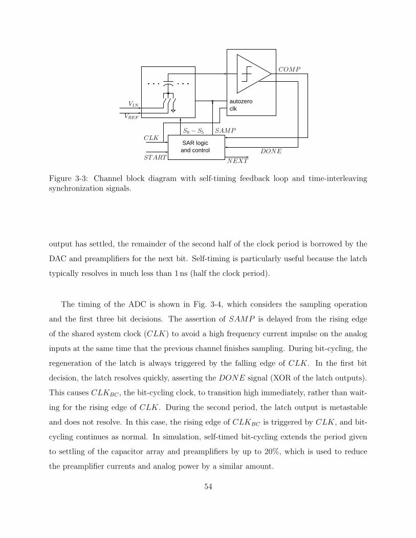
and controlSAR logic
clkautozero
VREF
CLK
START
COMP
SAMPS0 − S5
VIN
DONE
NEXT
Figure 3-3: Channel block diagram with self-timing feedback loop and time-interleavingsynchronization signals.
output has settled, the remainder of the second half of the clock period is borrowed by the
DAC and preamplifiers for the next bit. Self-timing is particularly useful because the latch
typically resolves in much less than 1 ns (half the clock period).
The timing of the ADC is shown in Fig. 3-4, which considers the sampling operation
and the first three bit decisions. The assertion of SAMP is delayed from the rising edge
of the shared system clock (CLK) to avoid a high frequency current impulse on the analog
inputs at the same time that the previous channel finishes sampling. During bit-cycling, the
regeneration of the latch is always triggered by the falling edge of CLK. In the first bit
decision, the latch resolves quickly, asserting the DONE signal (XOR of the latch outputs).
This causes CLKBC , the bit-cycling clock, to transition high immediately, rather than wait-
ing for the rising edge of CLK. During the second period, the latch output is metastable
and does not resolve. In this case, the rising edge of CLKBC is triggered by CLK, and bit-
cycling continues as normal. In simulation, self-timed bit-cycling extends the period given
to settling of the capacitor array and preamplifiers by up to 20%, which is used to reduce
the preamplifier currents and analog power by a similar amount.
54

Figure 3-4: Timing diagram showing sampling and the first three periods of bit-cycling. Inthe first bit-cycle, the DONE signal triggers CLKBC to start the next bit-cycle, whereasthe second period shows that bit-cycling is triggered by CLK when the latch is metastable.
3.2.2 SAR Logic
To implement a fast SAR controller, the logic, shown in Fig. 3-5, consists of a shift register
(SR0−SR5) and a set of switch drive registers (SW0−SW4). This topology allows the larger
switch drive registers to be clocked only once per conversion as opposed to every clock period
like the smaller shift registers, while keeping the critical path delay to only 2tc−q, where tc−q
is the delay from the rising clock edge to valid outputs of a register. The current bit being
resolved is determined by L4 − L0, only one of which is high every period. Si asserts on the
rising edge of Li at the start of the decision period for bit i. When Li falls, the decision for
that bit is made, bringing Si back low only if COMP is high.
Both the shift registers and the switch drive registers are implemented using full custom
dynamic logic. The shift registers SR0 − SR1 are conventional C2MOS registers, while
SR2 − SR5 have been modified as shown in Fig. 3-6. Transistors M1 − M4 and M9 − M12
form two C2MOS latches, with M13 − M14 producing the complementary output. M5 − M6
provide a reset operation, ending bit-cycling whenever START is received by the channel.
When this channel is not enabled (e.g., due to bit scaling, see Section 3.2.4), M7 −M8 force
Li low.
The switch drive logic function is implemented in the single register shown in Fig. 3-7.
Transistor M1 provides a fast charge path for Si upon the rising edge of Li. M4 − M7 form
55

D Q D Q D Q
D
RS
T
Q D
RS
T
Q
D Q
D
RS
T
Q D
RS
T
QD
RS
T
Q
D QD Q D Q
SampleGen
SR1 SR3 SR4 SR5
L4 L3 L2 L1 L0
CLKBC
SW1 SW2 SW3 SW4
S4 S3 S0S1S2
SW0
SAMP
START
SR0 SR′0CLK
NEXT
COMP
SR2
Figure 3-5: SAR logic implementation. The shift registers SR0−SR5 clock one of the switchdrive registers SW0 − SW4 during every phase of bit-cycling. The outputs S0 − S4 controlthe DAC capacitor array.
a C2MOS latch that holds the value of COMP after the falling edge of Li and discharges
Si through M2 − M3. During sampling, M12 − M14 reset Si low. Transistors M8 − M10 are
used to precharge node a to avoid charge sharing effects when M2 turns on. Finally, M11
puts the register in a known state when disabled.
Using this custom logic allows a faster and lower power SAR implementation. In sim-
ulations, the custom logic was 58% faster while consuming only 20% of the power of an
equivalent SAR built using static CMOS and transmission gate feedback flip-flops.
3.2.3 Comparator Design
The comparator of Fig. 2-3 has been modified as seen in Fig. 3-8(a) by adding preamplifier
enable signals and switches Sp2. The preamplifiers, shown in Fig. 3-8(b), have been designed
using the equations presented in Sec. 2.1.3, with M5 added to enable duty cycling. PMOS
transistors M3 − M4 operate in the linear region and function as the loads RL. The bias
current density has been set by considering (2.8). Ignoring the second term, minimum energy
corresponds to operating at low α (high gm/ID), which suggests operating in moderate to
weak inversion. Unfortunately, the fT of the transistors drops in moderate inversion, and
a suitable current density in strong inversion has been chosen to enable the high operating
56
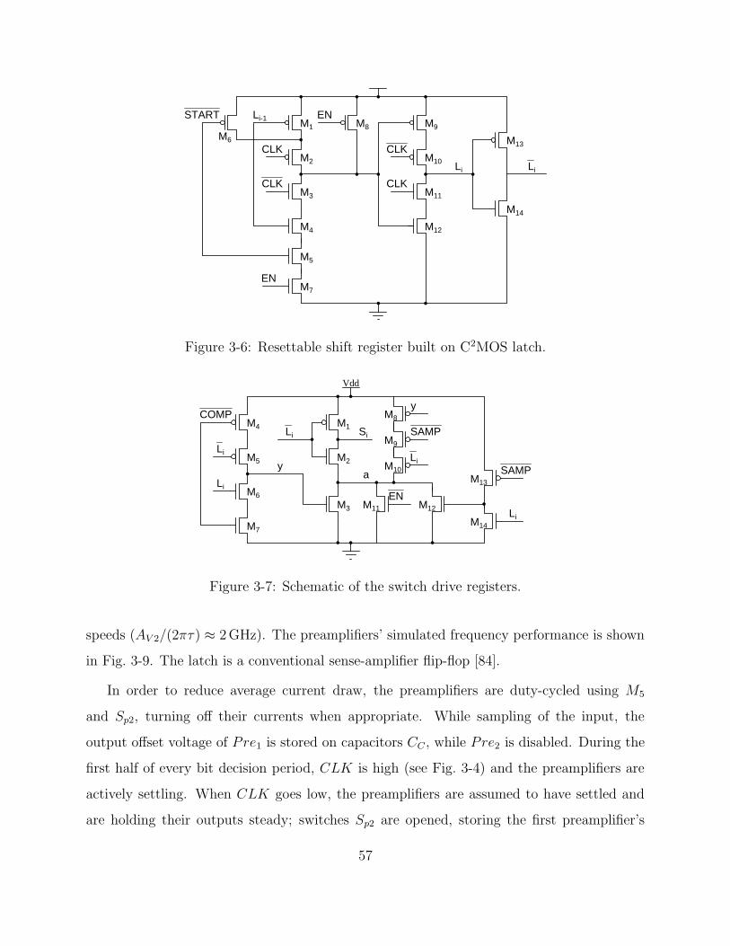
M11
CLK
Li-1
CLK
START
EN
EN
CLK
CLK
Li Li
M1
M2
M3
M4
M5
M7
M8 M9
M10
M12
M13
M14
M6
Figure 3-6: Resettable shift register built on C2MOS latch.
M4
M5
M6
M7
M1
M2
M3 M12
M14
M13
Li
Li
Li
Li
Si
COMP
SAMPya
Vdd
EN
SAMP
y
Li
M11
M10
M9
M8
Figure 3-7: Schematic of the switch drive registers.
speeds (AV 2/(2πτ) ≈ 2 GHz). The preamplifiers’ simulated frequency performance is shown
in Fig. 3-9. The latch is a conventional sense-amplifier flip-flop [84].
In order to reduce average current draw, the preamplifiers are duty-cycled using M5
and Sp2, turning off their currents when appropriate. While sampling of the input, the
output offset voltage of Pre1 is stored on capacitors CC , while Pre2 is disabled. During the
first half of every bit decision period, CLK is high (see Fig. 3-4) and the preamplifiers are
actively settling. When CLK goes low, the preamplifiers are assumed to have settled and
are holding their outputs steady; switches Sp2 are opened, storing the first preamplifier’s
57
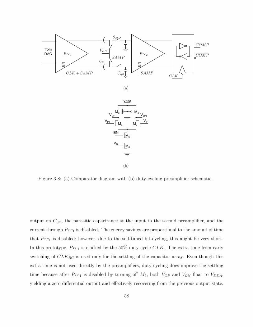
EN
EN
fromDAC Pre1 Pre2
COMP
COMP
CLKCip2
Sp2
CC
SAMP
VDD
SAMPCLK + SAMP
(a)
Vdda
VON
VIP
VOP
VIN
EN
VBM6
M5
M3 M4
M1 M2
(b)
Figure 3-8: (a) Comparator diagram with (b) duty-cycling preamplifier schematic.
output on Cip2, the parasitic capacitance at the input to the second preamplifier, and the
current through Pre1 is disabled. The energy savings are proportional to the amount of time
that Pre1 is disabled; however, due to the self-timed bit-cycling, this might be very short.
In this prototype, Pre1 is clocked by the 50% duty cycle CLK. The extra time from early
switching of CLKBC is used only for the settling of the capacitor array. Even though this
extra time is not used directly by the preamplifiers, duty cycling does improve the settling
time because after Pre1 is disabled by turning off M5, both VOP and VON float to VDDA,
yielding a zero differential output and effectively recovering from the previous output state.
58

108
109
1010
−20
−15
−10
−5
0
5
10
15
20
Gai
n (d
B)
Frequency (Hz)
TotalPre1Pre2
(a)
108
109
1010
−250
−200
−150
−100
−50
0
Pha
se (
degr
ees)
Frequency (Hz)
(b)
Figure 3-9: Simulated (a) gain and (b) phase of the preamplifiers.
3.2.4 Bit-scaling and I/O Circuits
For flexibility in response to varying system requirements, the ADC is capable of scaling its
resolution b from 1 to 5 bits at a constant sampling rate. Since each channel takes b + 1
periods to perform a conversion, fewer channels are needed to maintain the same throughput;
the unused 5 − b channels are disabled by stopping the propagation of the START signal,
gating the clocks, and shutting off all bias currents. The start generation block triggers the
first channel at a higher rate. When a channel receives the START signal, it samples during
the next clock period, and the sampling operation automatically ends bit decisions at the
correct, lower resolution.
To reduce circuit board requirements between the ADC and the digital back-end of the
UWB transceiver, the outputs of the channels are not serialized, yielding an output frequency
of 83 MHz. When not operating in the full 5-bit mode, some of the channels are deactivated.
Rather than placing the burden on the back-end chip to sort the ADC outputs, a mux tree
(see Fig. 3-1) is implemented to maintain a constant 83 MHz output rate independent of the
resolution, with the unused LSBs of each word forced to 0. Level conversion circuits are
placed between the core ADC and the I/O circuits to allow an internal digital supply lower
59

Time Per. Ch 1 Ch 2 Ch 3 Ch 4 Ch 5 Ch 61 S BD 0 BD 1 BD 2 BD 3 BD 42 BD 4 S BD 0 BD 1 BD 2 BD 33 BD 3 BD 4 S BD 0 BD 1 BD 24 BD 2 BD 3 BD 4 S BD 0 BD 15 BD 1 BD 2 BD 3 BD 4 S BD 06 BD 0 BD 1 BD 2 BD 3 BD 4 S
(a)
Time Per. Ch 1 Ch 2 Ch 3 Ch 4 Ch 5 Ch 61 S BD 2 BD 3 BD 4 OFF OFF2 BD 4 S BD 2 BD 3 OFF OFF3 BD 3 BD 4 S BD 2 OFF OFF4 BD 2 BD 3 BD 4 S OFF OFF5 S BD 2 BD 3 BD 4 OFF OFF6 BD 4 S BD 2 BD 3 OFF OFF
(b)
Figure 3-10: Table of states for all channels operating under (a) 5-bit and (b) 3-bit resolution.In the tables, S represents sampling, and BD is the bit decision phase for bit i. For thelower resolution modes, OFF means that the clocks are gated and all bias currents are shutdown.
than 1.8 V while still maintaining the proper voltage for inter-chip communication.
3.3 Measured Results
The dual ADC chip was fabricated in a 0.18-µm CMOS process with poly-poly capacitors.
The photograph of the 5.5 mm2 die is shown in Fig. 3-11. The active area of each ADC is
1 mm x 0.5 mm. With a 500 MHz sampling clock, the ADC exhibits an INL and DNL of
−0.26/0.42 and −0.39/0.33 LSBs, respectively, as shown in Fig. 3-12 and measured using a
code density test with a full swing sinusoidal input [85].
For dynamic testing, the Tektronix AWG710 arbitrary waveform generator was used to
generate the sinusoidal input using an 8-bit 4 GS/s DAC. The AWG710 also provided the
60

Figure 3-11: Die photograph of dual-ADC chip in 0.18-µm CMOS. Total active area is1.1 mm2.
0 10 20 30−0.5
−0.25
0
0.25
0.5
INL
(LS
B)
Code
(a)
0 10 20 30−0.5
−0.25
0
0.25
0.5
DN
L (L
SB
)
Code
(b)
Figure 3-12: Plot of the (a) INL and (b) DNL versus output code at 500MS/s.
500 MHz system clock; this clock source provides <5 ps rms jitter. The dynamic performance
at 500 MS/s is shown in Fig. 3-13(a). The periodic behavior of the SNDR is due to the
time-interleaving. At the peaks of the SNDR curve, the input frequency is aliased, with
reference to the channel sampling rate, to low frequencies. The low ERBW is a result of
insufficient settling time in the input sampling network. This is verified with the SNDR
plot of Fig. 3-13(b) measured at 125 MS/s, where the ERBW exceeds Nyquist with much
61
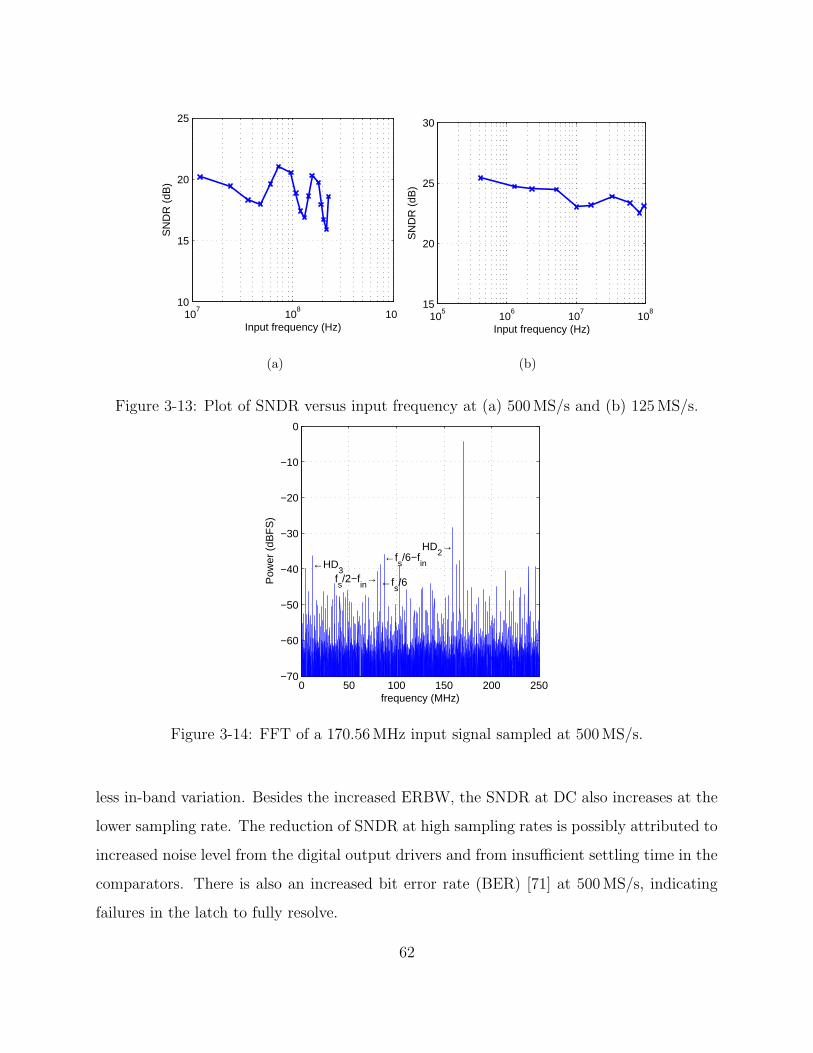
107
108
109
10
15
20
25
SN
DR
(dB
)
Input frequency (Hz)
(a)
105
106
107
108
15
20
25
30
SN
DR
(dB
)
Input frequency (Hz)
(b)
Figure 3-13: Plot of SNDR versus input frequency at (a) 500 MS/s and (b) 125 MS/s.
0 50 100 150 200 250−70
−60
−50
−40
−30
−20
−10
0
frequency (MHz)
Pow
er (
dBF
S)
HD2→
←HD3
fs/2−f
in→
←fs/6−f
in
←fs/6
Figure 3-14: FFT of a 170.56 MHz input signal sampled at 500 MS/s.
less in-band variation. Besides the increased ERBW, the SNDR at DC also increases at the
lower sampling rate. The reduction of SNDR at high sampling rates is possibly attributed to
increased noise level from the digital output drivers and from insufficient settling time in the
comparators. There is also an increased bit error rate (BER) [71] at 500 MS/s, indicating
failures in the latch to fully resolve.
62

1 2 3 4 50
1
2
3
4
5
6
7
8
Pow
er (
mW
)
Resolution (bits)
Analog powerDigital power
Figure 3-15: Analog and digital power consumption versus resolution for 500MS/s operation.
The FFT of a 170.56 MHz input sampled at 500 MS/s is shown in Fig. 3-14. The dominant
harmonics are labeled. The spurs from offset between channels at multiples of fs/6 and from
timing skew at fs/6 ± fin are comparable to those of the third harmonic at -38 dBFS. The
spurious free dynamic range (SFDR) is better than 24 dB, and the total harmonic distortion
(THD) is better than -15 dB for input frequencies up to over 300 MHz.
Each ADC draws 810µA from a 1.2-V analog supply and 3.6 mA from a 1.8-V digital
supply, for a total I/Q power consumption of 14.9 mW. Separating out the power for the
comparators’ latches (1.25 mW) from the total digital power, the logic consumes roughly 2.4
times the power of the comparators (the power drawn by the capacitor array is negligible).
The energy model in Chapter 2 predicts that this ratio should be 3.7 (see Fig. 2-6). The
difference is a result of optimization of the digital logic compared to the first model and the
preamplifiers operating at a non-optimum bias point; as the ratio is lower than predicted,
this further supports the original choice of SAR over flash.
The prototype includes an optional mode to disable the duty cycling of the preamplifiers.
Duty cycling reduces the analog power by 15% at 500 MS/s and by 26% at 125 MS/s. At
lower clock frequencies, the savings are greater because the overhead to charge and discharge
the output capacitances of the preamplifiers is reduced in comparison to the energy savings
over the longer time period that currents are disabled. Power dissipation versus resolution is
63
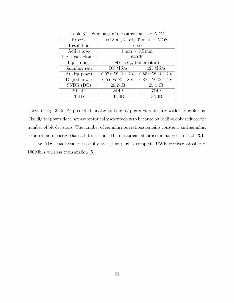
Table 3.1: Summary of measurements per ADC
Process 0.18µm, 2 poly, 5 metal CMOSResolution 5 bitsActive area 1 mm × 0.5 mm
Input capacitance 640 fFInput range 800 mVpp (differential)
Sampling rate 500 MS/s 125 MS/sAnalog power 0.97 mW @ 1.2 V 0.85 mW @ 1.2 VDigital power 6.5 mW @ 1.8 V 0.82 mW @ 1.4 VSNDR (DC) 20.2 dB 25.4 dB
SFDR 24 dB 39 dBTHD -16 dB -36 dB
shown in Fig. 3-15. As predicted, analog and digital power vary linearly with the resolution.
The digital power does not asymptotically approach zero because bit scaling only reduces the
number of bit decisions. The number of sampling operations remains constant, and sampling
requires more energy than a bit decision. The measurements are summarized in Table 3.1.
The ADC has been successfully tested as part a complete UWB receiver capable of
100 Mb/s wireless transmission [5].
64
Chapter 4
Prototype Featuring Split Capacitor
Array in Deep Sub-Micron CMOS
While the dynamic performance was not as strong as originally targeted, the first chip
still achieved low overall power numbers. Looking at the results, the power is completely
dominated by the switching power of digital circuitry, a problem that is usually not mentioned
in the ADC literature (although see Chapter 5 to realize how common this problem is).
In addition, while one of the primary challenges in porting analog designs to advanced
technologies is designing for operation at the reduced voltage supplies, the analog supply
voltage in the first testchip is at 1.2 V, already near or within the maximum voltage limits of
deep sub-micron CMOS processes. The comparator achieves its gain through cascading and
positive feedback, and it does not require cascoding or other techniques that increase the
minimum supply voltage. Also, the performance of the passive capacitor array is determined
primarily by matching and the speed of the switches. Thus, the SAR architecture, with its
medium digital complexity, passive capacitor array, and comparator, seems better suited for
implementation in more advanced technologies than an operational-amplifier based pipelined
converter.
This chapter presents the design of a second ADC prototype, which is implemented in
a low leakage 65-nm CMOS technology. Reduced feature sizes directly benefit the digital
65

logic controller, the block that limited the speed and power of the first prototype, but
it introduces new challenges for analog circuitry, which suffer from reduced intrinsic gain
and voltage headroom. This prototype implements a new capacitor array DAC structure,
termed the split capacitor array, that maximally conserves charge during a conversion while
exhibiting superior linearity than the binary weighted capacitive DAC without an increase
in area. The self-timed bit-cycling used in the first chip is replaced with a delay-line based
approach to adjust the latch strobing instant for increased preamplifier settling time in every
bit decision, including the first. These features are described below, followed by measurement
results demonstrating state-of-the-art performance.
4.1 A Foray into Charge Conservation: The SAR Ca-
pacitive DAC
The DAC serves two purposes in a SAR converter; it samples the input charge, and it gen-
erates an error voltage between the input and current digital estimate. The conventional
DAC choice is a binary-weighted capacitor array [28], as shown in Fig. 4-1. Unlike the alter-
native serial DAC [86] or C−2C ladder [87] structures, the linearity of this binary weighted
capacitor array is insensitive to parasitic capacitance between any of its nodes and ground.
This array, however, uses charge inefficiently during a conversion. This section begins with
an energy analysis of the conventional array structure and three different switching methods
with successively improved energy efficiencies. Then, the split capacitor array is introduced,
which is a new structure that retains all the benefits of the conventional array, but has
reduced switching energy, improved linearity, and faster switching speed.
All the array structures share common functionality to implement the SAR algorithm.
At the start of a conversion, Ssample is high, and the entire capacitor array stores the voltage
VMID − VIN . Then, at time 0, the MSB cap, Cb is connected to VREF , causing VX to settle
to
VX [1] = −VIN +VREF
2. (4.1)
66

Sb-1
Ssample
S1-S1
+
Ssample
S0-S0
+
Ssample
C0C1=C0Cb-1=2b-2C0
VX
Sb+
Ssample
Sb-
VREFVIN
...Cb=2b-1C0
+Sb-1
-
Sj-=Ssample+Sj
+ Ssample
Figure 4-1: Conventional b-bit binary weighted capacitor array.
The comparator’s output is then
D1 =
1 VIN < VREF /2
0 VIN > VREF /2(4.2)
The comparator’s output controls the next switch transition. If D1 is low, the second largest
capacitor is connected to VREF (S+b−1 = 1), raising the voltage at VX (I will call this an “up”
transition). If, on the other hand, D1 is high, Cb is returned to ground and Cb−1 is connected
to VREF (a “down” transition).
The above process is repeated for successive capacitors in the array. At each stage, the
value of VX , after switching transients have settled, is
VX = −VIN +CT
CT + CB
VREF (4.3)
where CT is the sum of all capacitors connected to the reference voltage, and CB is the sum
of all capacitors connected to ground:
CT =∑
i
2i−1C0 for i such that S+i = 1 (4.4)
CB =∑
i
2i−1C0 for i such that S+i = 0 (4.5)
67
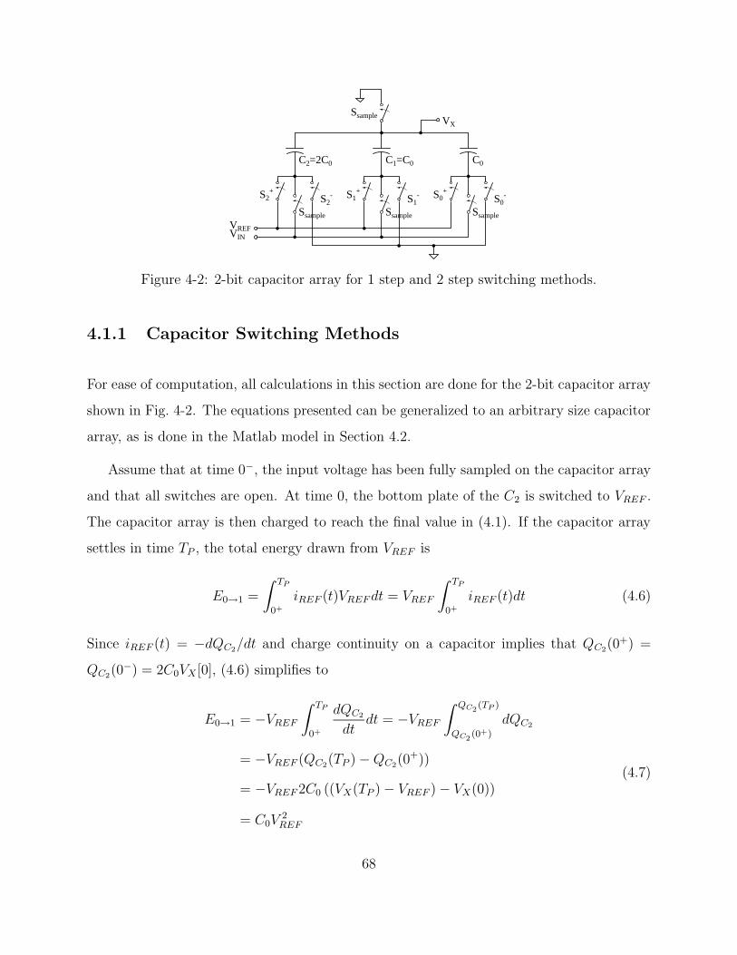
S2-S2
+
Ssample
S1-S1
+
Ssample
S0-S0
+
Ssample
C0C1=C0C2=2C0
VX
VREFVIN
Ssample
Figure 4-2: 2-bit capacitor array for 1 step and 2 step switching methods.
4.1.1 Capacitor Switching Methods
For ease of computation, all calculations in this section are done for the 2-bit capacitor array
shown in Fig. 4-2. The equations presented can be generalized to an arbitrary size capacitor
array, as is done in the Matlab model in Section 4.2.
Assume that at time 0−, the input voltage has been fully sampled on the capacitor array
and that all switches are open. At time 0, the bottom plate of the C2 is switched to VREF .
The capacitor array is then charged to reach the final value in (4.1). If the capacitor array
settles in time TP , the total energy drawn from VREF is
E0→1 =
∫ TP
0+
iREF (t)VREF dt = VREF
∫ TP
0+
iREF (t)dt (4.6)
Since iREF (t) = −dQC2/dt and charge continuity on a capacitor implies that QC2
(0+) =
QC2(0−) = 2C0VX [0], (4.6) simplifies to
E0→1 = −VREF
∫ TP
0+
dQC2
dtdt = −VREF
∫ QC2(TP )
QC2(0+)
dQC2
= −VREF (QC2(TP ) − QC2
(0+))
= −VREF 2C0 ((VX(TP ) − VREF ) − VX(0))(4.7)
= C0V2REF
68

VX
VREF
C0
C2=2C0
C1=C0
VX
VREF
C0
C1
C2
Figure 4-3: A “down” transition for the 1 step switching method.
This result matches the intuition that the effective series capacitance of the array, C0, must
be charged from 0 to VREF . The notation VX [i] will be used in the following calculations
to indicate the value of (4.3) after all transients have died out for the i’th transition, or,
equivalently, VX [i] = VX(i · TP ).
At the end of the first bit decision period, the sign of the voltage at the top plate of the
capacitor array is compared to VMID, producing D1. If D1 is 0, C1 in Fig. 4-2 is connected
to VREF , which is termed an “up” transition; all four switching methods behave identically
in this case. The total energy drawn from VREF for an “up” transition can be computed as
follows:
VX [2] = −VIN +3
4VREF (4.8)
E1→2 = −VREF [2C0 ((VX [2] − VREF ) − (VX [1] − VREF ))
+ C0 ((VX [2] − VREF ) − VX [1])] (4.9)
=C0V
2REF
4
The following subsections present four different methods of performing the “down” tran-
sition if D1 is 1 instead of 0.
4.1.2 Conventional One Step Switching
For a “down” transition, C2 is switched down to ground and C1 is connected to VREF .
The most straightforward method to perform this transition is to switch the two capacitors
simultaneously as shown in Fig. 4-3. The energy drawn from VREF while the capacitor array
69
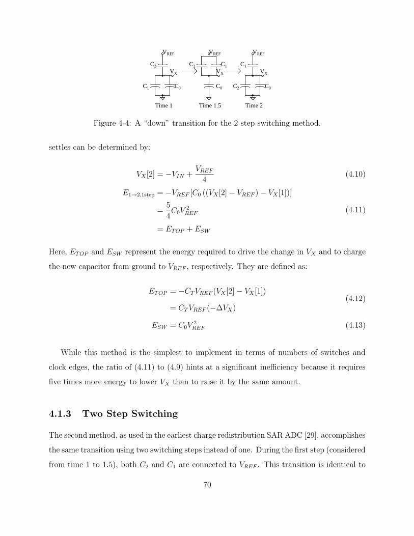
VX
VREF
C0
C2
C1
VX
C0
C1C2
VX
VREF
C0
C1
C2
Time 1 Time 1.5 Time 2
VREF
Figure 4-4: A “down” transition for the 2 step switching method.
settles can be determined by:
VX [2] = −VIN +VREF
4(4.10)
E1→2,1step = −VREF [C0 ((VX [2] − VREF ) − VX [1])]
=5
4C0V
2REF
= ETOP + ESW
(4.11)
Here, ETOP and ESW represent the energy required to drive the change in VX and to charge
the new capacitor from ground to VREF , respectively. They are defined as:
ETOP = −CT VREF (VX [2] − VX [1])
= CT VREF (−∆VX)(4.12)
ESW = C0V2REF (4.13)
While this method is the simplest to implement in terms of numbers of switches and
clock edges, the ratio of (4.11) to (4.9) hints at a significant inefficiency because it requires
five times more energy to lower VX than to raise it by the same amount.
4.1.3 Two Step Switching
The second method, as used in the earliest charge redistribution SAR ADC [29], accomplishes
the same transition using two switching steps instead of one. During the first step (considered
from time 1 to 1.5), both C2 and C1 are connected to VREF . This transition is identical to
70

S2-S2
+
Ssample
S1-S1
+
Ssample
S0-S0
+
Ssample
C0C1=C0C2=2C0
VX
VREFVIN
SCS
Ssample
(a)
VX
VREF
C0
C2
C1
VX
VC
C0
C1C2
VX
VREF
C0
C1
C2
Time 1 Time 1.5 Time 2
(b)
Figure 4-5: Capacitor (a) array and (b) equivalent circuits for the charge sharing method.When S+
2 = S+1 = 0 and SCS = 1, C1 is charged up from C2 with no energy drawn from the
supply.
that in (4.8)–(4.9). Then, at time 1.5, the largest capacitor is disconnected from VREF and
connected to ground, as seen in Fig. 4-4, drawing energy
E1.5→2 = −C0VREF (VX [2] − VX [1.5])
=C0V
2REF
2.
(4.14)
The total switching energy is thus
E1→2,2step = E1→1.5 + E1.5→2 =3
4C0V
2REF
= ETOP + ESW + 2C0VREF ∆VX
(4.15)
Since VX [2] < VX [1], the last term above is negative and (4.15) is less than (4.11).
Qualitatively, some of the charge transferred to C1 is reused from C2, similar to a charge
recovery scheme in switching of large data buses [88].
4.1.4 Charge Sharing (CS)
The previous subsection shows that energy savings can be achieved by using some of the
charge from the largest capacitor to charge up the second capacitor. An extension of this
71

method can be used for additional savings. Fig. 4-5(a) shows a modified capacitor array,
with an additional switch SCS. As in the above subsection, the switching is done in two
phases, as seen in Fig. 4-5(b). In the first phase, the first two capacitors are disconnected
from VREF and ground and connected to each other through the new switch. During this
phase, no energy is drawn from VREF . Using charge conservation, the voltage at node VC at
the end of the first phase is
VC [1.5] =2
3VREF
Therefore, the MSB/2 capacitor is effectively charged to two-thirds of the reference voltage
with zero energy expenditure.
During the second phase, the MSB capacitor is connected to ground and the MSB/2
capacitor is connected to VREF . The total energy dissipated is therefore
E1→2,CS = −C0VREF ((VX [2] − VREF ) − (VX [1] − VC))
=7
12C0V
2REF = ETOP +
1
3ESW . (4.16)
4.1.5 Split Capacitor Array
Even though charge sharing can save much of the energy in a “down” transition, some energy
must still be spent charging up C1 to VREF (namely, the total energy includes a contribution
from ESW ). To avoid charging any capacitor to VREF during a “down” transition, the final
method splits the MSB capacitor into two capacitors of value C0, and then switches down
one of them. This capacitor splitting results in the capacitor array shown in Fig. 4-6(a).
During the first bit decision, C2,1 and C2,0 are both connected to VREF , dissipating the
energy (4.7). After time 1, instead of connecting C1 to VREF , C2,1 is simply connected
directly to ground, as in Fig. 4-6(b). This requires the energy
E1→2,split = −VREF C0(VX [2] − VX [1])
=1
4C0V
2REF = ETOP
(4.17)
72

S2,0
Ssample
S1-
Ssample
S0-S0
+
Ssample
C0C1=C0C2,0=C0
VX
Ssample
C2,1=C0
VREFVIN
-S2,0+
S2,1-S2,1
+S1
+
Ssample
(a)
VX
VREF
C0
C2,1=C0
C1=C0
VX
VREF
C0
C2,0
C2,1
C2,0=C0
C1
(b)
Figure 4-6: The (a) modified array and (b) switching method for a two-bit capacitor arraywhere C2 has been split into two sub-capacitors, C2,1 and C2,0.
Thus, the capacitor splitting approach requires no energy spent to charge up a capacitor
from ground to VREF during a “down” transition and has achieved the same energy for an
“up” and a “down” transition.
The generalized b-bit split capacitor array is shown in Fig. 4-7; the MSB capacitor of the
conventional array has been split into an identical copy (MSB subarray) of the rest of the
array (main subarray). These arrays are placed in parallel (common top plate), not to be
confused with the series connected capacitor arrays used in the sub-DAC approach.1 The
total capacitance of the split capacitor array is 2bC0 and identical to the conventional array.
Because the capacitor array is usually arranged using a common centroid layout of multiple
unit capacitors, no extra area is required. This approach requires twice as many switches;
however, switches are generally small, so the area penalty is minimal.
The complete switching procedure is shown in Fig. 4-8. During the first bit cycle, all
capacitors Cb,0 . . . Cb,b−1 in the MSB subarray are connected to VREF . For subsequent “up”
transitions, the Ci in the main subarray is connected to VREF , while for any “down” transi-
tion, the MSB subarray capacitor Cb,i is connected to ground.
1Historically, the combination of capacitive main- and sub-DACs had been called a “ ‘split’ array” [42],but this has not become common usage, and I have co-opted the term for the new structure.
73

Sb-1
Ssample
S1-S1
+
Ssample
S0-S0
+
Ssample
C0C1=C0Cb-1=2b-2C0
VX
VREFVIN
...+
Sb-1-
Sb,b-1
Ssample Ssample Ssample
Cb,0=C0Cb,1=C0Cb,b-1=2b-2C0
...+
Sb,b-1- Sb,1
+ Sb,0+
Sb,0- Sb,0
-
Ssample
Figure 4-7: b-bit split capacitor array, with the main subarray on top and the MSB subarraybelow.
4.2 Energy Simulation Results
The above four switching methods have been applied to a 10-bit capacitor array. A Matlab
model using generalized forms of (4.9), (4.11)-(4.13), and (4.15)-(4.17) has been developed.
Fig. 4-9 compares this model to an HSPICE simulation of a 10-bit capacitor array in a
CMOS 0.18 µm process.
As can be seen in the figure, neglecting parasitics on the bottom plate of the capacitors
causes the model to greatly underestimate the energy. The best capacitors available on
the process are poly-poly capacitors with a 20fF parasitic bottom plate capacitance for
C0 = 100fF.
The simulations show clearly the energy savings that can be achieved using the different
methodologies. At the highest output code, all transitions are “up,” so all of the switching
methodologies require the same energy. At lower output codes, more “down” transitions
occur in the array, and the split capacitor array exhibits its greatest energy savings.
The average overall switching energy for a uniformly distributed input signal as well as
74

Start Bit-CyclingSsample = 0
Sb−1 = · · · = S0 = 0Sb,b−1 = · · · = Sb,0 = 1
i = b − 1
SamplingSsample = 1
Sb−1 = · · · = S0 = 0Sb,b−1 = · · · = Sb,0 = 0
Is VX > 0
“up”
i = i − 1Si = 1Sb,i = 1
“down”
i = i − 1Si = 0Sb,i = 0
Done
y = Sb−1Sb−2 . . . S0
Is i ≥ 0
yesno
yes
no
Figure 4-8: Switching procedure for split capacitor array. i represents the bit currently beingdecided.
for a full swing sinusoidal input can be calculated from the simulated data. The capacitor
splitting method saves 37% of the switching energy compared to the conventional one step
switching scheme. A comparison of the four switching methods is presented in Table 4.1.
The split capacitor array also draws current more evenly from a reference voltage buffer, if
used. Both the overall current requirement is reduced, and any signal-dependent even-order
nonlinearities of this current draw are eliminated.
75

0 200 400 600 800 10005
10
15
20
25
30
Output code
Sw
itchi
ng e
nerg
y (p
J)
1−Step2−StepCharge sharingSplit CapacitorSplit (no parasitics)
Figure 4-9: Plot showing the energy versus output code required for the switching of thecapacitor array. The HSPICE data points are plotted against the Matlab models (solidlines). The bottom curve shows the effect of parasitics on the Matlab model.
Table 4.1: Switching methodology energy comparison
Method EUP EDOW N# of # of
Euniform EsineSwitches Phases
1 step ETOP + ESW ETOP + ESW b + 1 1 1.000 1.000
2 step ETOP + ESWETOP + ESW
−2iC0VREF ∆VXb + 1 2 0.897 0.893
CS ETOP + ESW ETOP + ESW /3 2b 2 0.760 0.749
Splitting ETOP + ESW ETOP 2b 1 0.635 0.623
4.2.1 Switching Speed
For this high-speed implementation, an additional advantage of considerable significance
is related to the array’s settling time. During a “down” transition, two capacitors are
required to switch for the conventional capacitor array; any mismatch, whether random
or deterministic, in the digital logic driving these switches can cause the capacitor array to
initially transition in the wrong direction, potentially exacerbating an overdrive condition for
the preamplifiers. Only one capacitor in the split capacitor array transitions during any bit
decision, providing inherent immunity to the skew of the switch signals. Simulation results
comparing the settling times of the two arrays are shown in Fig. 4-10. For the simulations,
the total width of the switches is identical for the split and conventional arrays. The split
76

0 0.2 0.4 0.6 0.8 1−0.1
0
0.1
0.2
0.3
0.4
0.5
Time (normalized)
Diff
eren
tial v
olta
ge (
V)
SplitConv.
Figure 4-10: Simulation of the settling time of the split and conventional capacitor arraysunder the presence of digital timing skew.
capacitor array settles up to 10% faster, which is used to reduce the bias currents in the
preamplifiers by a similar amount.
4.2.2 Linearity Performance
To compare the theoretical static linearity of the binary-weighted and split DACs, each of
the capacitors is modeled as the sum of the nominal capacitance value and some error term:
Cn = 2n−1C0 + δn
Cb,n = 2n−1C0 + δb,n.(4.18)
Initially, consider only the case where all the errors are in the unit capacitors, whose values are
independent identically-distributed (i.i.d.) Gaussian random variables; later in this section,
other non-idealities will be considered. Then the error terms δn and δb,n have zero mean, are
independent, and have variance
E[
δ2n
]
= E[
δ2b,n
]
= 2n−1σ20, (4.19)
where σ0 is the standard deviation of the unit capacitor.
77
The linearity of a SAR ADC is limited by the accuracy of the DAC outputs, which are
calculated here for the case of no initial charge on the array (VIN = 0). For a given DAC
digital input y =∑b
n=1 Sn2n−1, with Sn equals 0 or 1 represents the ADC decision for bit n,
the analog output for the conventional binary-weighted array is
VX,conv(y) =
∑bn=1 (2n−1C0 + δn) Sn
2bC0 + ∆CVREF . (4.20)
The second term in the denominator ∆C =∑b
n=0 δn will be neglected for this discussion.
This will make the analysis simpler but will prevent a complete closed form solution for
the integral nonlinearity (INL); see Appendix B for an analysis without this approximation.
Subtracting the nominal value yields the error term
Verr(y) ≈∑b
n=1 δnSn
2bC0
VREF (4.21)
with variance
E[
V 2err(y)
]
=
∑bn=1 2n−1σ2
0Sn
22bC20
V 2REF
=y
22b
σ20
C20
V 2REF .
(4.22)
The voltage error in (4.21) and (4.22) is the sum of the errors from y unit capacitors connected
to VREF . Because the errors in the unit capacitors are assumed to be i.i.d., it does not matter
which unit capacitors are connected to VREF but only the total number. Thus (4.22) holds
for the case of the split capacitor array as well. This error is also directly related to the INL
of the ADC, and thus there should be no difference between the maximum INLs of the two
arrays.
The differential nonlinearity (DNL) of the capacitive DAC is, neglecting gain errors, the
difference between the voltage errors at two consecutive DAC outputs, as in
DNL(y) ≈ ∆Verr(y) = Verr(y) − Verr(y − 1). (4.23)
78

The worst case DNL for the binary weighted capacitor array is expected to occur at the step
below the MSB transition, where its variance is
E[
∆V 2err
(
2b−1)]
= E
(
δb −∑b−1
n=1 δn
2bC0
VREF
)2
≈ σ20
2bC20
V 2REF .
(4.24)
For the split capacitor array, the worst case DNL also occurs at the step below the MSB
transition, but its value is
∆Verr
(
2b−1)
=
∑b−1n=0 δb,n −
(
∑b−2n=0 δb,n +
∑b−2n=1 δn
)
2bC0
VREF
=δb,b−1 −
∑b−2n=1 δn
2bC0
VREF .
(4.25)
This error has a variance of
E[
∆V 2err
(
2b−1)]
≈ 1
2
σ20
2bC20
V 2REF . (4.26)
Comparing (4.24) and (4.26) shows that the standard deviation of the worst-case DNL is√
2
lower for the split capacitor array. Conceptually, this occurs because the errors at y = 2b−1
and y = 2b−1−1 are partially correlated for the split capacitor array, causing the cancellation
of δb,0, . . . , δb,b−2 in (4.25). This can be also be seen in the energy example above. In Fig. 4-
3, the errors of the top capacitors are completely uncorrelated for the two bit decisions;
however, in Fig. 4-6(b), the error of C2,0 contributes equally to both bit decisions.
A behavioral simulation of the SAR ADC, with both the binary weighted and split
capacitor arrays, was performed. The values of the unit capacitors are taken to be Gaussian
random variables with standard deviation of 3% (σ0/C0 = 0.03), and the ADC is otherwise
ideal. Fig. 4-11 shows the results of 10000 Monte Carlo runs, where the standard deviation
of the INL and DNL are plotted versus output code at the 5-bit level. As expected, the
conventional and split arrays have identical INL characteristics, and the split capacitor array
79
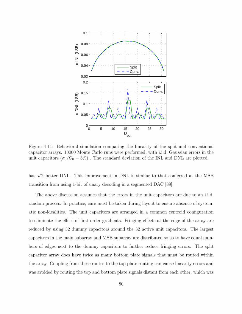
0.02
0.04
0.06
0.08
0.1
σ IN
L (L
SB
)
SplitConv.
0 5 10 15 20 25 300
0.05
0.1
0.15
0.2
σ D
NL
(LS
B)
Dout
SplitConv.
Figure 4-11: Behavioral simulation comparing the linearity of the split and conventionalcapacitor arrays. 10000 Monte Carlo runs were performed, with i.i.d. Gaussian errors in theunit capacitors (σ0/C0 = 3%) . The standard deviation of the INL and DNL are plotted.
has√
2 better DNL. This improvement in DNL is similar to that conferred at the MSB
transition from using 1-bit of unary decoding in a segmented DAC [89].
The above discussion assumes that the errors in the unit capacitors are due to an i.i.d.
random process. In practice, care must be taken during layout to ensure absence of system-
atic non-idealities. The unit capacitors are arranged in a common centroid configuration
to eliminate the effect of first order gradients. Fringing effects at the edge of the array are
reduced by using 32 dummy capacitors around the 32 active unit capacitors. The largest
capacitors in the main subarray and MSB subarray are distributed so as to have equal num-
bers of edges next to the dummy capacitors to further reduce fringing errors. The split
capacitor array does have twice as many bottom plate signals that must be routed within
the array. Coupling from these routes to the top plate routing can cause linearity errors and
was avoided by routing the top and bottom plate signals distant from each other, which was
80
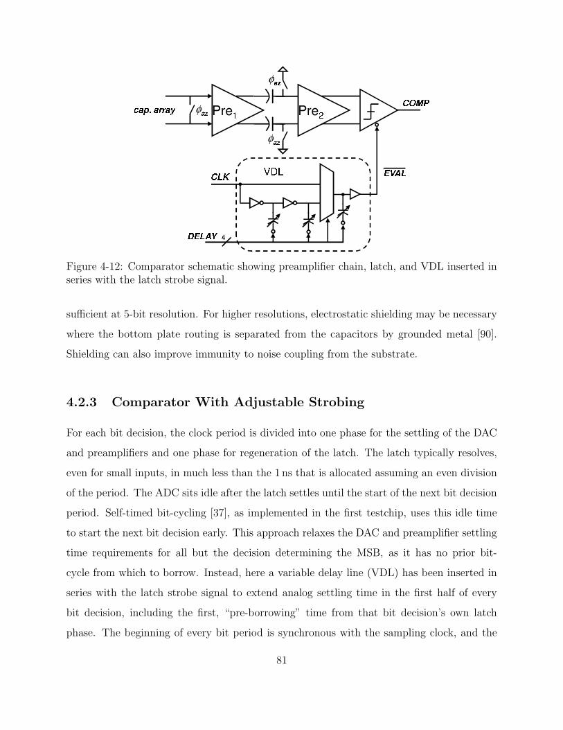
Figure 4-12: Comparator schematic showing preamplifier chain, latch, and VDL inserted inseries with the latch strobe signal.
sufficient at 5-bit resolution. For higher resolutions, electrostatic shielding may be necessary
where the bottom plate routing is separated from the capacitors by grounded metal [90].
Shielding can also improve immunity to noise coupling from the substrate.
4.2.3 Comparator With Adjustable Strobing
For each bit decision, the clock period is divided into one phase for the settling of the DAC
and preamplifiers and one phase for regeneration of the latch. The latch typically resolves,
even for small inputs, in much less than the 1 ns that is allocated assuming an even division
of the period. The ADC sits idle after the latch settles until the start of the next bit decision
period. Self-timed bit-cycling [37], as implemented in the first testchip, uses this idle time
to start the next bit decision early. This approach relaxes the DAC and preamplifier settling
time requirements for all but the decision determining the MSB, as it has no prior bit-
cycle from which to borrow. Instead, here a variable delay line (VDL) has been inserted in
series with the latch strobe signal to extend analog settling time in the first half of every
bit decision, including the first, “pre-borrowing” time from that bit decision’s own latch
phase. The beginning of every bit period is synchronous with the sampling clock, and the
81
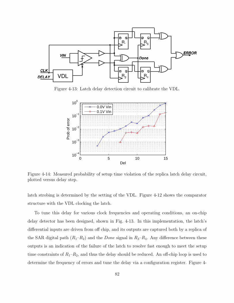
Figure 4-13: Latch delay detection circuit to calibrate the VDL.
0 5 10 1510
−4
10−3
10−2
10−1
100
Pro
b of
err
or
Del
0.0V Vin0.1V Vin
Figure 4-14: Measured probability of setup time violation of the replica latch delay circuit,plotted versus delay step.
latch strobing is determined by the setting of the VDL. Figure 4-12 shows the comparator
structure with the VDL clocking the latch.
To tune this delay for various clock frequencies and operating conditions, an on-chip
delay detector has been designed, shown in Fig. 4-13. In this implementation, the latch’s
differential inputs are driven from off chip, and its outputs are captured both by a replica of
the SAR digital path (R1–R2) and the Done signal in R3–R4. Any difference between these
outputs is an indication of the failure of the latch to resolve fast enough to meet the setup
time constraints of R1–R2, and thus the delay should be reduced. An off-chip loop is used to
determine the frequency of errors and tune the delay via a configuration register. Figure 4-
82

14 plots the probability of a setup time violation versus the delay step for two differential
input voltages. As expected, for a larger input voltage or shorter delay step, fewer setup
time violations occur. The reduced error at delay step 10 is due to non-monotonicity in the
VDL at this step. While the control loop’s function is simple enough to implement on chip
with a counter and simple finite state machine, this circuit exhibits a very high sensitivity
to the input referred offset voltage of the replica latch. For a fixed differential input voltage,
chosen to be zero for convenience, the delay of the replica latch to reach an output differential
voltage of Vlatch is [91]
tdlatch ≈ to + τ ln
[
kVlatch
VOS
]
. (4.27)
Here, τ = C/Gm is the time constant of regeneration, and k and to are topology and process
dependent. As VOS approaches zero, the second term in (4.27) increases without bound.
Thus, this replica delay circuit can only be used to set the delay of the in-channel latches if
the differential input voltage can be adjusted. An alternative approach is to directly embed
the latch delay detection circuit within each channel. Busy input signals would exercise the
entire input range of the latch, and actual latch errors can be detected and the delay step
backed off accordingly. The delay calibration could be done continuously or shut down once
a sufficiently low error rate is achieved. In the implemented prototype, the replica delay
detection circuit was used, with its differential input controlled manually.
4.2.4 Technology Considerations
In 65-nm CMOS, The SAR architecture’s digital complexity directly benefits from the re-
duced feature sizes. Even though this ADC uses a fully static CMOS logic style, it still
consumes less power than the highly customized logic, including dynamic registers, used
in the first testchip. Care was taken throughout the digital logic to provide the maximum
robustness in presence of delay variations.
The two analog blocks are well suited for integration in deep sub-micron CMOS with
the following design considerations. For the same absolute device size, transistor matching
improves in successive technology generations, allowing smaller total device area and capac-
83

Figure 4-15: Photograph of 1.9 × 1.4 mm2 die.
itance in the comparators [92]; however, the matching is not improved for minimum size
devices. Also, due to the reduced power supplies and decreased gmro of the short channel
devices, it is difficult to get high gain in a single analog stage. The preamplifiers and latch
use non-minimum length transistors to improve both the matching and output impedance.
While this does increase device capacitance for the same gm, there is only a small power
impact because the extracted wiring parasitics, which do not scale with the gate length, are
65% of the total load capacitance for the first preamplifier.
The capacitor array is entirely passive, and its switching speed is improved with the
shorter gate lengths. Because no analog-specific processing steps (e.g., a thin oxide for
high density MiM capacitors) were used in fabrication the capacitors are formed using in-
terdigitated metal comb capacitors. The capacitance is determined by fringing between
adjacent metal lines, structures that have been shown to achieve similar densities to MiM
capacitors with matching limits at greater than the 7-bit level [93]. The capacitance size is
chosen according to the matching requirements discussed in Section 4.1. The input voltage
is constrained to between 0 and 400 mV to allow sampling with a single standard-VT NFET
transistor without exceeding the process voltage limit of 1.2 V.
84

0 10 20 30
−0.2
−0.1
0
0.1
0.2
0.3
INL
(LS
B)
Output code0 10 20 30
−0.2
−0.1
0
0.1
0.2
0.3
DN
L (L
SB
)
Output code
Figure 4-16: Static linearity of ADC versus output code.
−0.5
0
0.5
INL
(LS
B)
0 10 20 30
−0.5
0
0.5
DN
L (L
SB
)
Output code
(a)
−0.5
0
0.5IN
L (L
SB
)
0 10 20 30
−0.5
0
0.5
DN
L (L
SB
)
Output code
(b)
Figure 4-17: Comparison of the static linearity for the (a) conventional capacitor array and(b) the worst case split capacitor array channel on the same die.
4.3 Measurements
The ADC has been fabricated in a 65-nm CMOS technology; a die photograph is shown
in Fig. 4-15. With a 91-kHz input sampled at 500 MS/s, the INL and DNL are -0.16/0.15
and -0.25/0.26 LSBs, respectively (Fig. 4-16). A separate test channel with the conventional
85

105
10
15
20
25
30
35
40
45
50
fin
(Hz)
dB
SNDRSFDRTHD
Figure 4-18: Dynamic performance versus input frequency.
capacitor array and one-step switching method is located on the upper right corner of the die.
A direct comparison indicates that the split capacitor array uses 31% less power from the
400 mV reference voltage supply; the difference in energy savings from the theory presented
above is due to the increased bottom-plate routing. The static linearity of the reference
channel is plotted in Fig. 4-17(a) and has a peak DNL/INL of 0.76/0.56 LSBs. This is
significantly higher than the overall ADC nonlinearity; however, the statistical measures
used to calculate linearity [85] average any uncorrelated errors between channels, producing
up to a√
6 improvement in static linearity for the interleaved results. A more suitable
comparison is with a single channel. Figure 4-17(b) plots the static linearity of the worst
case split capacitor channel on the same die as the conventional channel. While a direct
comparison favors the split capacitor array, these results may be skewed by less diligent
layout of the conventional array, leading to increased nonlinear coupling of the bottom plate
to top plate routing.
The delay line was tested using the on-chip delay detection circuit and varying the input
differential voltage, as shown in Fig. 4-14. Due to an underestimation of parasitics in the
delay line, only the first 2 delay steps out of 16 provided sufficient time for latch regeneration,
and these extended the period available to the preamplifiers by about 10%. At 250 MS/s, a
86

0 50 100 150 200 250−90
−80
−70
−60
−50
−40
−30
−20
−10
0
Frequency (MHz)
dBF
S hg
Spurs
(a) fs/2−f
in
(b) fs/3−f
in
(c) fs/6−f
in
(d) fs/6+f
in
(e) fs/6
(f) fs/3
(g) HD5
(h) HD3
e
fb
ad
c
Figure 4-19: FFT of 239.04-MHz sine wave sampled at 500 MS/s; dominant spurs are labeled.
0.5-1 dB improvement in SNDR was achieved by properly tuning the delay.
The dynamic performance of the ADC is shown in Fig. 4-18 with the input frequency
swept from DC to beyond Nyquist. The SNDR does not drop by 3 dB until past the Nyquist
frequency. An FFT of a 239.04-MHz input is shown in Fig. 4-19. Spurs (a)-(d) result from
gain errors and skew between channels, and spurs (e)-(f) are due to offset mismatch. All of
these spurs are below -39 dBFS, and their combined power is still less than the total noise
power (excluding the spurs) at this near-Nyquist input. The gain mismatch between channels
is 0.9%. The individual channels have a low frequency effective number of bits (ENOB)
between 4.65 and 4.75 that drops by 0.4 bits at Nyquist.
The ADC consumes 2.86 mW and 3.06 mW, respectively, from 1.2 V analog and digital
supplies at the maximum sampling frequency. The ADC was also tested at lower sampling
frequencies. At 250 MS/s, the ADC consumes a total of 1.58 mW from a 1 V digital and
0.8 V analog supply, while still maintaining Nyquist performance. A summary of the ADC
is listed in Table 4.2.
87
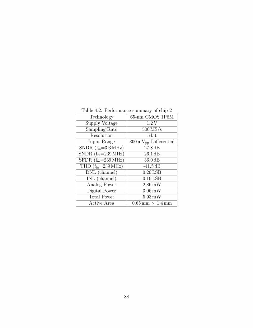
Table 4.2: Performance summary of chip 2
Technology 65-nm CMOS 1P6MSupply Voltage 1.2 VSampling Rate 500 MS/s
Resolution 5 bitInput Range 800 mVpp Differential
SNDR (fin=3.3 MHz) 27.8 dBSNDR (fin=239 MHz) 26.1 dBSFDR (fin=239 MHz) 36.0 dBTHD (fin=239 MHz) -41.5 dB
DNL (channel) 0.26 LSBINL (channel) 0.16 LSBAnalog Power 2.86 mWDigital Power 3.06 mWTotal Power 5.93 mWActive Area 0.65 mm × 1.4 mm
88

Chapter 5
Mixed-Signal Optimum Energy Point
The two ADC prototypes presented previously demonstrated both the potential for high-
speed SAR ADCs, and the energy-efficiency of this architecture. To further reduce the power,
an optimization is performed to find the operating point with minimum energy for this inter-
leaved SAR architecture. This chapter begins with a discussion of prior work in optimization
of analog and digital circuits. It is noted that the class of ADCs with both significant analog
and digital energy contributions cannot be optimized by focusing on the analog or digital
components separately, but a systematic joint design and optimization of both parts and
their interaction, must be performed. While optimization of the comparator energy was
performed based on the equations in Section 2.1.3, and joint timing design of the analog and
digital circuits was presented as part of the self-timing (Sec. 3.2.1) and VDL-based latch
strobe point adjustment (Sec. 4.2.3), this chapter presents a far more comprehensive joint
design of the analog and digital circuits. Timing is included in the model, including specific
interactions and feedbacks (e.g., loading), and additional independent variables are added.
In particular, the model is created to determine the optimum mixed-signal operating point,
as specified by supply voltage and level of parallelism. This operating point achieves roughly
3× energy savings in the same technology as compared to the ADC presented in the previous
chapter.
89

4 6 8 10 12 14 16 180
10
20
30
40
50
60
70
80
90
100
Nominal resolution (bits)
Dig
ital p
erce
ntag
e of
tota
l pow
er
SARFlashPipelinedFoldingSubranging
Figure 5-1: Relative digital power for published Nyquist ADCs that explicitly separate theanalog and digital power consumptions.
5.1 Overview of Traditional Circuit Optimization
Over time, most ADC research has focused on architectures and techniques to reduce analog
power. This has been encouraged by the scaling associated with Moore’s law that reduces
digital power in comparison with analog and enables greater digital integration on chip.
As a result of this trend, digital power is now a significant portion of the total dissipation
in many ADCs, particularly those operating at low resolutions and high speeds. Figure 5-1
shows the percentage of digital power contribution in recent papers that differentiate between
analog and digital power consumptions. While digital power can be significant across all the
resolutions, it is particularly so at low resolutions and cannot be ignored, even though it is
rarely mentioned in the literature.
SAR is an excellent architecture to demonstrate the advantage of joint analog and digital
design because digital logic limits the critical feedback path, and at low-to-medium resolu-
90
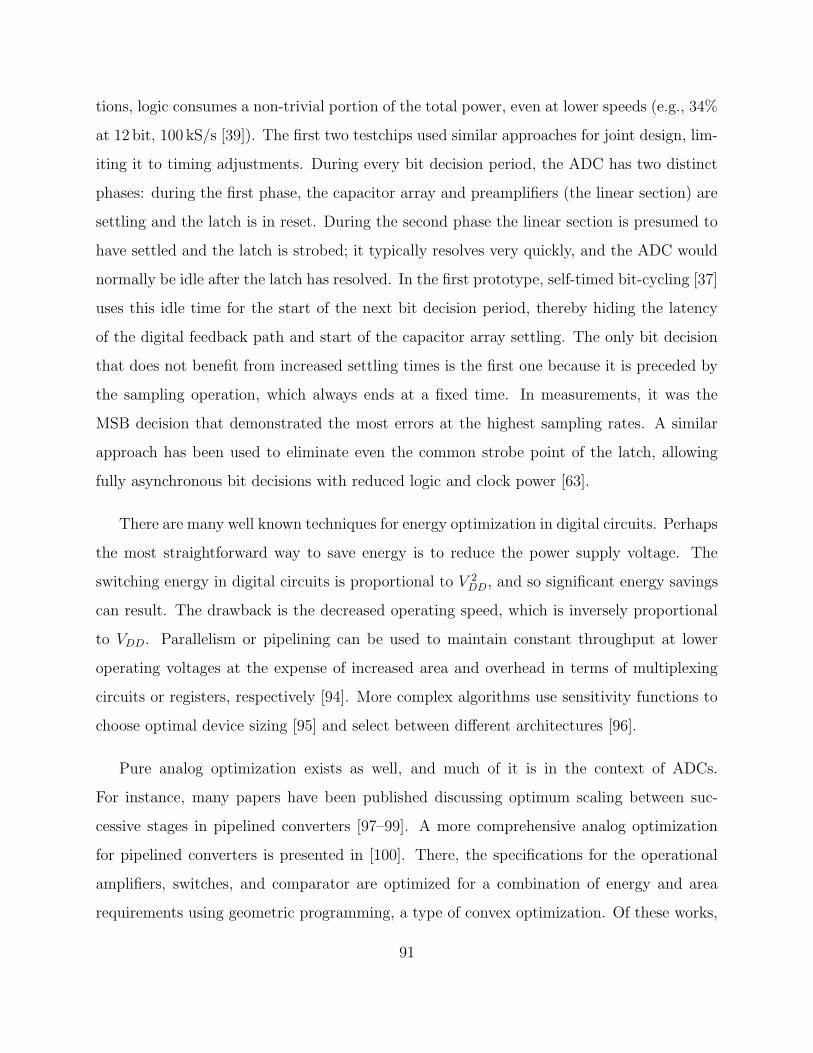
tions, logic consumes a non-trivial portion of the total power, even at lower speeds (e.g., 34%
at 12 bit, 100 kS/s [39]). The first two testchips used similar approaches for joint design, lim-
iting it to timing adjustments. During every bit decision period, the ADC has two distinct
phases: during the first phase, the capacitor array and preamplifiers (the linear section) are
settling and the latch is in reset. During the second phase the linear section is presumed to
have settled and the latch is strobed; it typically resolves very quickly, and the ADC would
normally be idle after the latch has resolved. In the first prototype, self-timed bit-cycling [37]
uses this idle time for the start of the next bit decision period, thereby hiding the latency
of the digital feedback path and start of the capacitor array settling. The only bit decision
that does not benefit from increased settling times is the first one because it is preceded by
the sampling operation, which always ends at a fixed time. In measurements, it was the
MSB decision that demonstrated the most errors at the highest sampling rates. A similar
approach has been used to eliminate even the common strobe point of the latch, allowing
fully asynchronous bit decisions with reduced logic and clock power [63].
There are many well known techniques for energy optimization in digital circuits. Perhaps
the most straightforward way to save energy is to reduce the power supply voltage. The
switching energy in digital circuits is proportional to V 2DD, and so significant energy savings
can result. The drawback is the decreased operating speed, which is inversely proportional
to VDD. Parallelism or pipelining can be used to maintain constant throughput at lower
operating voltages at the expense of increased area and overhead in terms of multiplexing
circuits or registers, respectively [94]. More complex algorithms use sensitivity functions to
choose optimal device sizing [95] and select between different architectures [96].
Pure analog optimization exists as well, and much of it is in the context of ADCs.
For instance, many papers have been published discussing optimum scaling between suc-
cessive stages in pipelined converters [97–99]. A more comprehensive analog optimization
for pipelined converters is presented in [100]. There, the specifications for the operational
amplifiers, switches, and comparator are optimized for a combination of energy and area
requirements using geometric programming, a type of convex optimization. Of these works,
91

only [97] addresses the digital circuitry, and only in a limited fashion. This chapter describes
a framework and model for comprehensive analog/digital optimization.
One challenge of optimization not addressed by this thesis is the speed that the opti-
mization can be solved. Discrete optimization is the broadest class of optimizations and the
most straightforward to formulate. Any problem can be written as a discrete optimization.
Unfortunately, without a lengthy exhaustive search of the design space, solutions may get
trapped in local minima without ever visiting the global optimum, and failure to find a solu-
tion does not guarantee that one does not exist. Del mar Hershenson has published several
papers describing setting up convex optimizations for analog circuitry and solving them using
geometric programming. Formulations have been presented for operational amplifiers [101],
inductors [102], LC-oscillators [103], phase-locked loops [104], amplifier chains [105], and
pipelined ADCs [100]. The major challenge is formulating the problem as a convex opti-
mization. Some constraints require significant manipulation to be made convex, and others
simply cannot be included. In particular, only simple transistor models are amenable to
convex formulations [101], and these models do not accurately characterize the behavior of
advanced short-channel devices. Once set up, however, geometric programming led to so-
lutions of complex design problems in much less than one minute, which would be almost
instantaneous on a modern microprocessor. In comparison, the discrete optimization formu-
lated in this chapter is solved in 20–30 minutes, making it less applicable for repeated design
iterations, but it is able to handle a much wider range of problem definitions with a shorter
setup time.
5.2 Modeling Methodology
This section describes the setup of the energy model and its simulation methodology. The
speed of solving the energy model is not a primary concern for this work. Instead, the model
emphasizes modularity for evaluating architectural changes and process independence. The
process parameters can be calculated and entered into the architecture-based model after the
fact. The formulated model ends up being a discrete optimization, the least efficient class of
92
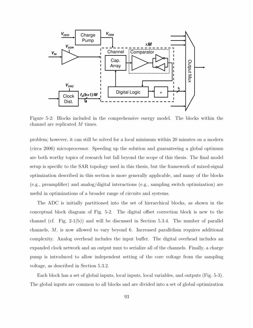
Figure 5-2: Blocks included in the comprehensive energy model. The blocks within thechannel are replicated M times.
problem; however, it can still be solved for a local minimum within 20 minutes on a modern
(circa 2006) microprocessor. Speeding up the solution and guaranteeing a global optimum
are both worthy topics of research but fall beyond the scope of this thesis. The final model
setup is specific to the SAR topology used in this thesis, but the framework of mixed-signal
optimization described in this section is more generally applicable, and many of the blocks
(e.g., preamplifier) and analog/digital interactions (e.g., sampling switch optimization) are
useful in optimizations of a broader range of circuits and systems.
The ADC is initially partitioned into the set of hierarchical blocks, as shown in the
conceptual block diagram of Fig. 5-2. The digital offset correction block is new to the
channel (cf. Fig. 2-1(b)) and will be discussed in Section 5.3.4. The number of parallel
channels, M , is now allowed to vary beyond 6. Increased parallelism requires additional
complexity. Analog overhead includes the input buffer. The digital overhead includes an
expanded clock network and an output mux to serialize all of the channels. Finally, a charge
pump is introduced to allow independent setting of the core voltage from the sampling
voltage, as described in Section 5.3.2.
Each block has a set of global inputs, local inputs, local variables, and outputs (Fig. 5-3).
The global inputs are common to all blocks and are divided into a set of global optimization
93

Sub−block2
Sub−block1GlobalParams
Block A
OA
G/A/P
I2L2
O2
G/A/P
I1L1
O1
IA
PAG LA (local vars)
Figure 5-3: Basic block structure for the energy model. There are three sets of inputs com-mon to all the blocks (G = global optimization parameters (e.g., VDDD), A = architecturalparameters (e.g., timing partition variables), and P = process-specific parameters (e.g., gm)).In addition, each block has its own specific inputs I, local variables L, and outputs O. Anyof these parameters may be passed to a sub-block contained within.
parameters, such as the voltage supplies, a set of architectural parameters that describe
some switches in the block structure, and a set of process parameters. Thus, in a different
technology, only the process parameters would have to change with an otherwise identical
optimization setup. The line between the global optimization parameters and the global
architectural parameters is arbitrary, as some of the global optimization parameters do re-
quire changes in the circuit topology, as in the sampling switch configuration described in
Appendix C.2.1. A list of the global parameters is listed in Table 5.1, along with the default
values and/or optimization ranges, as appropriate. These ranges are for the primary opti-
mization that directly leads to the design in the following chapter. Different sets of global
constraints are discussed at the end of this chapter.
The local inputs are determined by the enclosing block, or the top-level ADC if there is
no enclosing block, and they are often outputs of another block. For instance, the energy
required for the charge pump is determined by the total current drawn by the sampling
switches in the digital block. Thus, the outputs of the blocks include the energy per conver-
sion consumed as well as inputs for other blocks. This leads to the set of dependencies as
shown in Fig. 5-4. The arrow ⇒ indicates that output parameters of one block are required
to calculate the energy of another block. Because the actual number of connections between
blocks (i.e., the circuit’s signal path) is small, there are only a limited number of these model
94
Table 5.1: Global optimization parameters
Parameter Description Value/Range
b Converter resolution 5
fS Sampling frequency 500 MHz
M Number of time-interleaved channels ≥ 1
VDDD Core digital supply voltage 0.5–1.2 V
VDDA Core analog supply voltage VDDD
VFS Full scale input voltage 0.1 V–VDDD
VDDS Boosted sampling voltage VDDD–1.2 V
SWSAMP Sampling switch configuration (see App. C.2.1) N, TGSWREF Reference voltage switch configuration (see App. C.2.1) N, P
tconv Total conversion time for a channel M/fS
Figure 5-4: Data dependencies and solution order for the energy model blocks.
dependencies. The solution order (numbers in Fig. 5-4) is chosen such that each block’s en-
ergy is computed after all of its inputs are available. Two special cases can be seen where
there are bidirectional dependencies, and these require special consideration in the model
setup.
The first is within the comparator, where tradeoffs can be made between the size of
the latch and the power of the preamplifiers. Specifically, a larger latch increases its input
capacitance and switching energy but reduces the required preamplifier gain for a fixed
input referred offset voltage. The second complicated dependency involves the digital buffers
95

driving the switches in the capacitor array, where additional buffering stages are inserted
to drive the large fanout of the array. The added buffers decrease the time available for
settling within the array, requiring an increased switch size and potentially more buffering.
The methods to resolve these dependencies are discussed in the comparator and the channel
block descriptions.
For a fixed set of optimization parameter values, the SAR energy model returns the
energy per conversion, as well as the local variables that specify, among others, transistor
sizing throughout the comparator and buffering required between the logic block and the
capacitor array. There are some sets of optimization parameters, however, for which the
model fails to find a solution, mostly because no solution is possible. For instance, the
specification M = 1 and VDDD = 0.5 means a single 500 mV channel operating at 500 MS/s,
requiring an internal clock rate of 3 GHz. As the delay through a single digital gate at 500 mV
is much greater than 300 ps, no possible solution exists. The block descriptions below specify
under what conditions failures can arise. A failure in any block will cause a failure of the
entire SAR model. The optimization then searches the design space (Table 5.1) for the set
of global inputs that yield a functioning design with the minimum modeled energy.
5.3 Block Descriptions
This section describes the blocks of the energy model. The order of the block descriptions is
the same as the solution order in Fig. 5-4. Only the highlights and limitations of the block
models are presented here; detailed descriptions and equations are included in Appendix C,
along with a summary of the required process data.
5.3.1 Digital Logic
The energy of the digital logic within the channel is composed of the core energy necessary for
the logical function of the successive approximation register plus the fanout energy necessary
to drive the potentially large switches of the capacitor array. The former is fixed once
96

the resolution and supply voltage are set, and it is modeled identically to the model in
Section 2.1.1 (Edig,core ∝ bV 2DDD). The latter is dependent on and must be jointly optimized
with the capacitor array sizing. As the capacitive load of the capacitor array switches can
be large, buffering is automatically inserted to maintain a minimum size core controller with
no gate having a fanout exceeding 4.
The model, detailed in Appendix C.1, includes the effect of leakage currents and the
overhead for level shifting if a separate sampling supply voltage is used. In addition to the
energy in (C.6), the digital block also calculates the setup and propagation delays in (C.8)–
(C.10), which are required for the timing of the other blocks in the channel (see below). The
delays include the effect of the buffer insertion.
The energy and delay of digital logic vary across process corners, and delay in particular
can be significantly affected by local variations at lower voltages. The energy model only
handles a single corner and is not variation aware. While the optimum energy point will
change at different corners (e.g., more parallelism at higher digital energies), there will still
be a broad minimum (cf. Fig. 5-9(a)) and therefore a wide range of reasonable levels of
parallelism.
5.3.2 Capacitor Array
The capacitor array model from Section 2.1.2 is extended here to address the energy required
to sample a high frequency signal and switch the array to meet a settling time constraint.
The times available for sampling and switching are set by the channel block as described
below, and they are considered fixed within the capacitor array model.
During the sampling operation, all of the capacitors in the array are connected in parallel,
forming the basic sampling network shown in Fig. 5-5(a). The sampling network must
meet two basic requirements. When the sampling switches first close, the charge across the
capacitor must step from the previous stored value to the now, potentially different input
voltage. The transient from this step response must settle within the sampling window, and
this limits the maximum equivalent resistance of the two switches. Second, the network
97
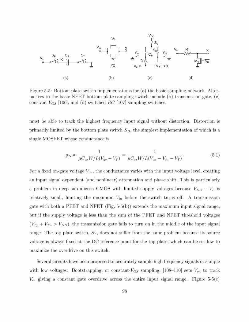
Vin
SB STCS
X
(a)
X
SB
Vin
SB
(b)
VDD
SB
SB
SB
SBSB
Vin X
CB
MS
(c)
Vin R1
MS SB
X
(d)
Figure 5-5: Bottom plate switch implementations for (a) the basic sampling network. Alter-natives to the basic NFET bottom plate sampling switch include (b) transmission gate, (c)constant-VGS [106], and (d) switched-RC [107] sampling switches.
must be able to track the highest frequency input signal without distortion. Distortion is
primarily limited by the bottom plate switch SB, the simplest implementation of which is a
single MOSFET whose conductance is
gds ≈1
µCoxW/L(Vgs − VT )=
1
µCoxW/L(Von − Vin − VT ). (5.1)
For a fixed on-gate voltage Von, the conductance varies with the input voltage level, creating
an input signal dependent (and nonlinear) attenuation and phase shift. This is particularly
a problem in deep sub-micron CMOS with limited supply voltages because VDD − VT is
relatively small, limiting the maximum Vin before the switch turns off. A transmission
gate with both a PFET and NFET (Fig. 5-5(b)) extends the maximum input signal range,
but if the supply voltage is less than the sum of the PFET and NFET threshold voltages
(VTp + VTn > VDD), the transmission gate fails to turn on in the middle of the input signal
range. The top plate switch, ST , does not suffer from the same problem because its source
voltage is always fixed at the DC reference point for the top plate, which can be set low to
maximize the overdrive on this switch.
Several circuits have been proposed to accurately sample high frequency signals or sample
with low voltages. Bootstrapping, or constant-VGS sampling, [108–110] sets Von to track
Vin giving a constant gate overdrive across the entire input signal range. Figure 5-5(c)
98

shows a simplified diagram of a bootstrapping network. Before sampling, during phase SB,
the sampling switch MS is turned off with its gate grounded. The boost capacitor CB is
precharged with a voltage VDD across it. Then, during the sampling period, CB is placed
between the input voltage and the gate of the sampling switch, setting the latter to VDD+Vin,
which makes the VGS of MS independent of the input signal voltage. The backgate effect
causes some residual input-signal conductance variation because of the dependence of VT on
VSB = Vin if the bulk is grounded. If a triple well process is available or PFET sampling is
used [111], VSB can be set to zero, eliminating this residual error, and more sophisticated
bootstrapping techniques have been proposed to adjust Von to track Vin + VT [112]. These
bootstrapping techniques add complexity and power to the channel design, and care must
be taken to avoid transients that can lead to voltages beyond the reliability limits of the
process.
Several papers use closed-loop sampling networks and switched opamps [113, 114] to
eliminate the floating series bottom plate switch, but these are not considered further here
because the use of an operational amplifier violates one of the key principles motivating this
thesis for design in deep sub-micron CMOS. Another approach, switched-RC sampling [107],
eliminates the series bottom plate switch without requiring an opamp. The bottom plate
switch is replaced with a series linear resistor and shunt switch, as shown in Fig. 5-5(d).
During the track phase, the series resistance is linear, and during the hold phase, the shunt
transistor MS with a maximum overdrive voltage, strongly connects the bottom plate of CS
to ground, attenuating the input at node X. The linearity is limited only by the residual
input signal at node X during the hold phase, but it leads to a DC current draw during the
hold phase. For higher input frequencies, R1 must be small to sample accurately, but the
hold current increases proportionately. Because of the very high maximum input frequencies,
the switched-RC network is not appropriate for the ADC considered in this thesis.
To simplify the design and minimize complexity within the channel, this model only
considers the simple NFET or transmission gate sampling networks but with an extra degree
of freedom, which allows the voltage VDDS driving the NFET gate to be higher than the core
99

digital voltage VDDD. This higher voltage can be generated using a charge pump, as discussed
in Section 5.3.9. VDDS is constrained to be within the process limit of 1.2 V, but this extra
degree of freedom allows the core voltage to be driven lower and provides overall energy
savings for the ADC (cf. Fig. 5-12). Appendix C.2.1 details the NFET sampling network.
The transmission gate requires a more complicated model setup and is described in its own
Appendix D. Appendix C.2.2 analyzes the switching of the array during the bit decision
periods, which is similar to the sampling setup but with only the settling time constraint
(i.e., no tracking requirements).
5.3.3 Comparator
The comparator model is designed to be more accurate and flexible than the model presented
in Chapter 2. The topology uses a cascade of low gain preamplifiers, each with OOS, followed
by a regenerative latch, but now the number of preamplifiers is variable. In addition, the
tradeoff between latch sizing, offset, capacitance, and energy is made explicitly, and effects
such as slewing and fixed wiring capacitances are included. Equations for the comparator,
preamplifier, and latch are given in Appendix C.3.
The model does not include any effect of circuit noise, which is not significant at 5 bits,
but it limits the applicability at higher resolutions. The direct effect of offset from local
variation is considered for the latch and completely eliminated by OOS for the preamplifiers;
however, mismatch can also reduce the effective gain of the preamplifiers below the model’s
output, particularly if the nominal gain is above 5.
5.3.4 Digital Offset Correction
Offset has two deleterious effects in interleaved ADCs. The first can be seen by considering
the digital output of an ADC
y[n] = Q (vIN [n] + vOS[n mod M ]) , (5.2)
100

where Q(·) represents the quantization function and vIN [n] is the sampled analog input
signal. For an interleaved ADC, the offset voltage vOS is periodic with the number of
channels, producing spurs in the output spectrum at multiples of fS/M , the channel sampling
frequency.
Offset produces a second effect, namely clipping of large input signals. The maximum
input dynamic range of an ADC is thereby reduced by the peak-to-peak offsets across the
channels. The first two testchips set the offset requirement of the comparator (i.e., the analog
offset) to make the power of the periodic term in (5.2) smaller than the quantization noise
power, namely
E[v2OS] = σ2
vOS<
V 2LSB
12. (5.3)
This condition forces the offset of every channel to be small (< VLSB), and the reduction in
dynamic range due to clipping is negligible.
Another approach to reducing the power of the periodic term in (5.2) is to correct it
digitally, which simply requires an adder1 [50,53]. Then, the analog offset requirements can
be set only to keep clipping within an acceptable limit. The effect of digital offset correction
is quantified using a coupling of the behavioral (see Appendix A) and energy models.
Figure 5-6 shows the SNDR of an interleaved ADC versus the analog offset voltage for
varying degrees of digital offset correction. The lower plot, with no offset correction, tails
off directly due to the effect of the periodic offset term in (5.2), while the upper curves, with
digital offset correction, only drop when clipping becomes significant. For the same 1 dB
degradation in SNDR, digitally correcting the offset to within a half an LSB permits using
a 6× larger analog offset voltage, although 3× is used to be conservative in this design.
The results of the behavioral model can then be fed back to the energy model. Specifically,
1While medium complexity calibration circuitry is required to determine the proper offset correction value,once calculated, the continual correction only requires an adder at the output of the channel. Section 6.3further explores the contrast between calibration and correction.
101
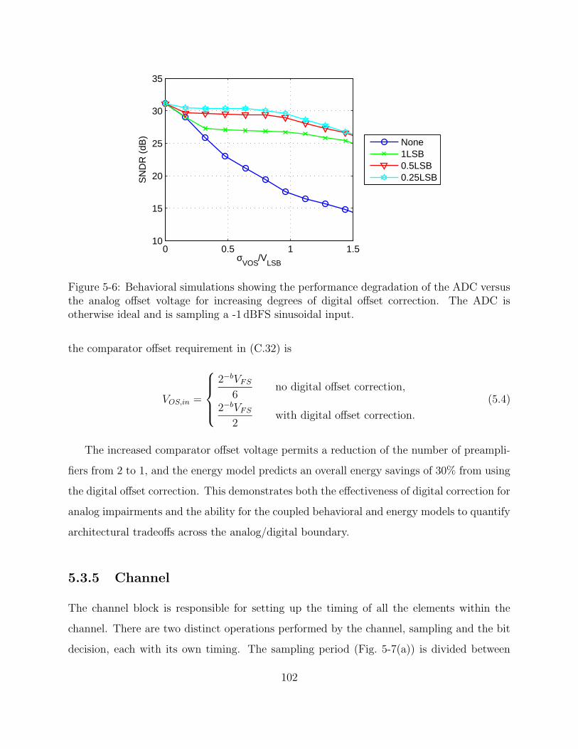
0 0.5 1 1.510
15
20
25
30
35
σVOS
/VLSB
SN
DR
(dB
)
None1LSB0.5LSB0.25LSB
Figure 5-6: Behavioral simulations showing the performance degradation of the ADC versusthe analog offset voltage for increasing degrees of digital offset correction. The ADC isotherwise ideal and is sampling a -1 dBFS sinusoidal input.
the comparator offset requirement in (C.32) is
VOS,in =
2−bVFS
6no digital offset correction,
2−bVFS
2with digital offset correction.
(5.4)
The increased comparator offset voltage permits a reduction of the number of preampli-
fiers from 2 to 1, and the energy model predicts an overall energy savings of 30% from using
the digital offset correction. This demonstrates both the effectiveness of digital correction for
analog impairments and the ability for the coupled behavioral and energy models to quantify
architectural tradeoffs across the analog/digital boundary.
5.3.5 Channel
The channel block is responsible for setting up the timing of all the elements within the
channel. There are two distinct operations performed by the channel, sampling and the bit
decision, each with its own timing. The sampling period (Fig. 5-7(a)) is divided between
102

tsample
tper = M/(fS(b + 1))
δtsamptper
tpd,samp
(a)
tper = M/(fS(b + 1))
tsetuptd,latch
tper/2
tpd,bc
1 − δtcapδtcap
tsettle,pre
(b)
Figure 5-7: Timing division of the (a) sample and (b) bit decision clock periods.
the digital logic and the capacitor array, with the total sampling window set as a fraction,
δtsamp, of a channel clock period (tconv/(b + 1)), as specified in (5.5). This fractional term
can be used to model architectural limitations to the length of the sampling window, such
as avoiding overlapped sampling windows between the parallel channels.
tsample =δtsamptconv
b + 1− tpd,samp (5.5)
The bit decision clock periods are split into two half clock periods. The first half clock
period consists of the propagation delay through the digital logic and the linear settling of the
capacitor array and preamplifiers. The rest of the clock period is used for the regeneration
time of the latch and the setup time of the digital logic, as shown in Fig. 5-7(b). The bit
decision period does not need to be split evenly between these two phases; the VDL of
Section 4.2.3 explicitly changes the timing between the two, which will be further examined
in the context of the energy model in Section 5.4.3. For the purposes of this section and the
final chip, the two phases will be of equal length. The linear analog settling time is split
between the array and preamplifiers with architectural parameter δtcap. This parameter can
itself be determined by adding it to the global optimization setup (Table 5.1), and the value
of 0.25 has been determined as optimal for the final results.
103

Appendix C.5 discusses the simulation setup to solve these timing constraints and focuses
on the interplay between the timing of the digital and capacitor array blocks.
5.3.6 Clock Distribution
Clock distribution is one of the principle overheads of highly interleaved ADCs because both
the number of clocks must increase and the die area across which the clocks are distributed
is increased. For the proposed energy model, the clock distribution is implemented using a
simple clock tree model. Generation (i.e., a PLL and dividers) is assumed to be handled at
a higher level of the system hierarchy. To minimize timing skew, the clock paths to every
channel should be balanced, which means that the paths to the closest and farthest channels
should have the same length. This can be accomplished by an H-tree [115] or similar network.
The length of the clock path to any channel therefore grows as the length from the center of
the die (presumed to be the origin of clock distribution) to the corner of the die (the location
of the farthest channel). If the die area grows with M , then the length of the clock path to
a single channel grows with√
M , making the per-channel clock capacitance
Cclk = Cclk0
√
M/M0, (5.6)
where measurements or parasitic extraction can be used to determine the capacitance Cclk0
for distributing the clock to one out of M0 channels. This equation, simple in form, is very
similar to the expected scaling of an H-tree’s capacitance, Cclkwire, with the number of gates,
Ng, in a digital circuit, which scales as Cclkwire ∝√
Ng [116].
The total energy per conversion is
Eclk = C ′clkV
2DDD(b + 1), (5.7)
where C ′clk is modified to include the energy required for buffering as in (C.3)–(C.5), and
a single conversion requires (b + 1) clock periods. This additional buffering will add to the
overall jitter of the sampling network but can be minimized with a sufficiently precise initial
104

1
2
kmux
M
Lmux
Figure 5-8: Mux tree to combine M channel outputs into a single ADC output, where eachline in the figure is a b-bit bus. Each stage reduces the number of outputs by kmux.
clock and using a quiet voltage supply for the clock buffer chain, which was the approach
chosen in the final testchip.
It is important to note that (5.7) only applies if the minimum frequency clock is dis-
tributed to every channel. If, instead, the sampling clock is distributed in a balanced path
to every channel, then (5.6) still applies for the path length, but the number of clock edges
per conversion increases from b + 1 to M , giving a total clock energy that grows as M 3/2
instead of M 1/2. Clearly, minimizing the frequency of the clock distribution is critical in
interleaved ADCs.
The final clock distribution described in Section 6.2.1 does not scale exactly with this
model because the clock paths to different channels vary in length and delay, but it is only
applicable to values of M that are multiples of (b+1), and this simple model with C ∝√
M
is still a reasonable, slightly conservative approximation.
5.3.7 Output Mux
For a typical application, the outputs of the individual channels must be combined into a
single output stream for the ADC. A scalable solution for this sorting is to use a tree of
105
multiplexers as shown in Fig. 5-8, where each stage in the tree reduces the number of outputs
by kmux. The total number of stages that the output of a single channel passes through is
Lmux = logkmuxM, (5.8)
and the total energy of the output mux is
Emux = bLmuxCsw,muxV2DDD. (5.9)
The prefactor b accounts for the b digital bits output by each channel, and Csw,mux includes
the switched capacitance of the mux itself plus the relatively large wiring capacitance in
between successive stages.
5.3.8 Input Buffer
The most significant analog overhead for increasing the number of interleaved channels is the
input capacitance that grows with increased routing and parasitic capacitance of the sampling
switches. If the input capacitance Cin of the ADC cannot be driven by the preceding stage
in the system, an input buffer is required. For the UWB system considered in this work,
the final baseband amplifier has an output impedance of RS = 50 Ω, and therefore an input
buffer is necessary only if
Cin ≥ 1
2πRSfS/2. (5.10)
If this condition is met exactly, the input will be attenuated by 3 dB at Nyquist, which is too
much attenuation for many applications. In practice, this condition should be exceeded by
a fair margin (4 to 10), which can be modeled by adding a factor of 1/kbackoff on the right
side of (5.10) to designate the target ratio of the input bandwidth to the Nyquist frequency.
Appendix C.8 includes the equations when an input buffer is necessary.
The model for the input buffer is simple, neglecting such effects as noise and linearity.
Because the final level of parallelism is below the point where an input buffer is necessary, a
106

more accurate or detailed model is not included.
5.3.9 Charge Pump
A charge pump is introduced to allow a decoupling of the sampling voltage from the core
supply voltage, as discussed above in Section 5.3.2. In the model, the energy of the charge
pump is directly related to the current of the sampling switch drivers and an efficiency
parameter, ηCP . The efficiency has been set to 70%, which is reasonable based on published
charge pumps [117,118]. The charge pump equations are given in Appendix C.9.
5.4 Model Results
The energy model has been implemented using Matlab with the global optimization parame-
ters defined in Table 5.1. Figure 5-9 plots the predicted energy per conversion and operating
voltages versus the number of parallel channels. The optimum energy point occurs with 60
channels at a 0.65-V core voltage, and the rapid increase in the right side of the curve corre-
sponds to the input capacitance when an input buffer becomes necessary (see Section 5.3.8).
The kink in the curve for small values of M occurs because of the overhead of the charge
pump. When M < 13, the core voltage is sufficiently high that the charge pump, with its
non-ideal efficiency ηCP , is not necessary.
One important observation from Fig. 5-9(a) is that the energy curve is fairly shallow,
with a broad minimum below the optimum energy point. The broadness of this minimum
can be understood by considering the breakdown of the energy among the various ADC
blocks, as shown in Fig. 5-10 for M=36. As VDDD is reduced, the dominant digital portion
of the energy decreases, but M increases significantly (see the flattening of the VDDD curve
at the right of Fig. 5-9(b)). This increases the clock and mux energies, but since they are
still a relatively small percentage of the overall power, their significant increase effectively
balances the decrease in core digital energy, making the minimum fairly broad.
Instead of trying to operate at the optimum energy point, using 24 or 36 parallel channels
107
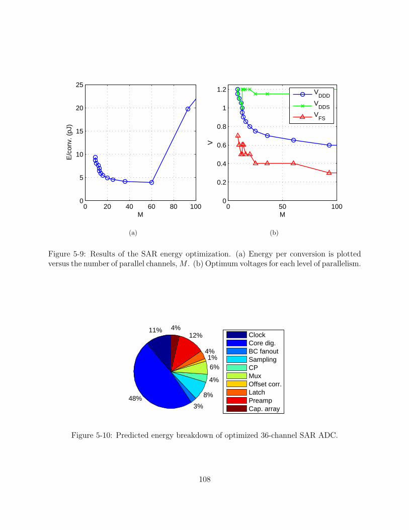
0 20 40 60 80 1000
5
10
15
20
25
M
E/c
onv.
(pJ
)
(a)
0 50 1000
0.2
0.4
0.6
0.8
1
1.2
MV
V
DDD
VDDS
VFS
(b)
Figure 5-9: Results of the SAR energy optimization. (a) Energy per conversion is plottedversus the number of parallel channels, M . (b) Optimum voltages for each level of parallelism.
11%
48%3%
8%
4%
6%1%
4%
12%4%
ClockCore dig.BC fanoutSamplingCPMuxOffset corr.LatchPreampCap. array
Figure 5-10: Predicted energy breakdown of optimized 36-channel SAR ADC.
108
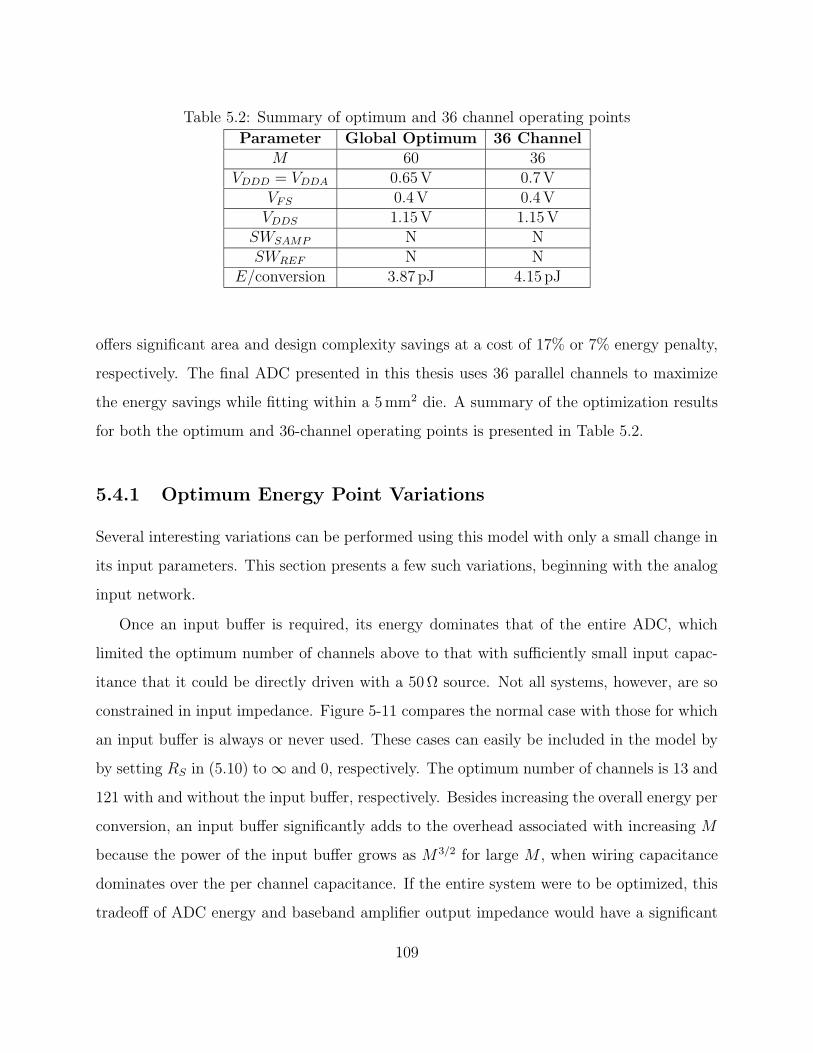
Table 5.2: Summary of optimum and 36 channel operating points
Parameter Global Optimum 36 ChannelM 60 36
VDDD = VDDA 0.65 V 0.7 VVFS 0.4 V 0.4 VVDDS 1.15 V 1.15 V
SWSAMP N NSWREF N N
E/conversion 3.87 pJ 4.15 pJ
offers significant area and design complexity savings at a cost of 17% or 7% energy penalty,
respectively. The final ADC presented in this thesis uses 36 parallel channels to maximize
the energy savings while fitting within a 5 mm2 die. A summary of the optimization results
for both the optimum and 36-channel operating points is presented in Table 5.2.
5.4.1 Optimum Energy Point Variations
Several interesting variations can be performed using this model with only a small change in
its input parameters. This section presents a few such variations, beginning with the analog
input network.
Once an input buffer is required, its energy dominates that of the entire ADC, which
limited the optimum number of channels above to that with sufficiently small input capac-
itance that it could be directly driven with a 50 Ω source. Not all systems, however, are so
constrained in input impedance. Figure 5-11 compares the normal case with those for which
an input buffer is always or never used. These cases can easily be included in the model by
by setting RS in (5.10) to ∞ and 0, respectively. The optimum number of channels is 13 and
121 with and without the input buffer, respectively. Besides increasing the overall energy per
conversion, an input buffer significantly adds to the overhead associated with increasing M
because the power of the input buffer grows as M 3/2 for large M , when wiring capacitance
dominates over the per channel capacitance. If the entire system were to be optimized, this
tradeoff of ADC energy and baseband amplifier output impedance would have a significant
109

0 20 40 60 80 1000
5
10
15
20
25
M
E/c
onv.
(pJ
)
Nominal (R
S=50Ω)
RS=0Ω
RS=∞
Figure 5-11: Modeled energy versus per conversion versus parallelism with varying sourceimpedances. With an ideal source, an input buffer is never necessary, leading to lowerenergy and higher optimum value of M than the case with infinite source impedance, alwaysrequiring an input buffer.
impact on the ADC optimum energy point.
Another input signal variant is related to the sampling supply. As mentioned above,
for small values of M , the overhead from the charge pump makes the use of a separate
sampling supply voltage inefficient. If a separate sampling supply is not desired or possible,
the optimization can be run with VDDD = VDDS , as compared with both the nominal case
and the case with no charge pump overhead in Fig. 5-12. As the supply voltage drops, the
sampling switches must rapidly increase in size to be able to track the constant frequency
input signal, and at 700 mV this causes a 22% energy penalty for the entire ADC. Below
600 mV, the ADC fails to operate for any value of M because τsw0 = Cpar0,B/gds0,B, the
inherent switch time constant is too large, making (C.15) negative.
The optimization parameter setup given in Table 5.1 constrains the analog and digital
supplies to operate at the same voltage. This is beneficial from a system complexity stand-
point because fewer voltage domains are required, but this constraint is not fundamental
to the model. An optimization has been performed allowing VDDA and VDDD to vary inde-
pendently. For the 36 channel operating point, the optimum analog voltage is only 50 mV
110
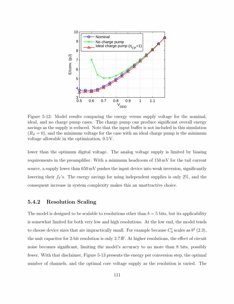
0.5 0.6 0.7 0.8 0.9 1 1.13
4
5
6
7
8
9
10
VDDD
E/c
onv.
(pJ
)
NominalNo charge pumpIdeal charge pump (η
CP=1)
Figure 5-12: Model results comparing the energy versus supply voltage for the nominal,ideal, and no charge pump cases. The charge pump can produce significant overall energysavings as the supply is reduced. Note that the input buffer is not included in this simulation(RS = 0), and the minimum voltage for the case with an ideal charge pump is the minimumvoltage allowable in the optimization, 0.5 V.
lower than the optimum digital voltage. The analog voltage supply is limited by biasing
requirements in the preamplifier. With a minimum headroom of 150 mV for the tail current
source, a supply lower than 650 mV pushes the input device into weak inversion, significantly
lowering their fT ’s. The energy savings for using independent supplies is only 2%, and the
consequent increase in system complexity makes this an unattractive choice.
5.4.2 Resolution Scaling
The model is designed to be scalable to resolutions other than b = 5 bits, but its applicability
is somewhat limited for both very low and high resolutions. At the low end, the model tends
to choose device sizes that are impractically small. For example because C ′0 scales as b2 (2.3),
the unit capacitor for 2-bit resolution is only 2.7 fF. At higher resolutions, the effect of circuit
noise becomes significant, limiting the model’s accuracy to no more than 8 bits, possibly
fewer. With that disclaimer, Figure 5-13 presents the energy per conversion step, the optimal
number of channels, and the optimal core voltage supply as the resolution is varied. The
111

2 4 6 80
500
1000
1500
2000
2500
Resolution
E/c
onve
rsio
n st
ep (
fJ)
(a)
2 4 6 80
100
Mop
t (o)
Resolution
0.5
0.75
1
1.2
Vdd
d (x)
(b)
Figure 5-13: Optimum energy point as a function of resolution. The energy per conversionstep (a) is the energy per conversion normalized to 2b. In (b) the optimum amount ofinterleaving and voltage supply are plotted.
energy per conversion step is the energy per conversion normalized to the ideal quantization
step (E/conv./2b). This is similar to the figure of merit (1.1) but using b instead of ENOB.
The energy per conversion step is not a monotonic function of resolution; instead, the linear
increase in core digital power with the resolution causes an overall decrease in the energy per
conversion step at medium resolutions, but at higher resolutions, the matching requirements
on the capacitor array and comparator produce an overall increase this metric. As shown
in Fig. 5-13(b), as the core digital percentage of power decreases at higher resolutions, the
optimal voltage supply increases, along with a corresponding decrease in the amount of
interleaving. The jump in M between 6 and 7 bits corresponds to the resolution when an
input buffer is always necessary due to the increase in capacitor sizing. If the input source
is ideal, then the optimal supply voltage still increases with the resolution, but the optimum
number of channels is far greater (200–300).
112

5.4.3 Architectural Tradeoffs: the VDL
Section 5.3.4 already presented how architectural tradeoffs can be quantified using the energy
model presented in this chapter, in that case demonstrating the significant energy savings
from adding digital offset correction at the output of every channel. Here, another example
will be presented, namely an examination of the energy savings for the VDL-based latch
strobe adjustment circuitry presented in Section 4.2.3.
The VDL was inserted to pre-borrow the idle time after the latch has resolved to extend
the preamplifier settling time. Considering Fig. 5-7(b), the idle time is the unused time in
the second half of the clock period,
tidle = tper/2 − td,latch − tsetup. (5.11)
Ideally, the VDL uses this idle time to extend the first half of the period, which can be
implemented by appropriately modifying the channel block.
At the chosen 36-channel operating point, the VDL increases the length of the first phase
of the bit decision period by 21%, but produces an overall energy savings of only 3%. The
savings are primarily due to reduced preamplifier current, which is not one of the dominant
contributors to power consumption. If the switching energy of the VDL is considered, there
are no net savings for using this approach.
5.4.4 Conclusion
This chapter has presented a comprehensive mixed signal energy model for use in opti-
mization and evaluation of architectural tradeoffs across the analog/digital boundary. The
primary optimization parameters are the amount of interleaving and the supply voltages.
Several architectural tradeoffs were analyzed, including digital offset correction, the use of a
separate sampling supply voltage, and the VDL-based latch strobe adjustment. The model
is set up to facilitate scaling to different technologies, requiring only simulations of the basic
building blocks and knowledge of the parasitics and matching. The chosen operating point
113

of 36 channels is within 10% of the optimal energy point of 93 channels but with significantly
less area and design complexity. The next chapter presents the implementation details of
this highly-interleaved ADC, with a specific emphasis of the challenges of highly parallel
mixed-signal design and the pronounced effects of local variation.
114

Chapter 6
Highly-Parallel ADC With Channel
Redundancy
This chapter describes the design, implementation, and measurements of a highly parallel
ADC, the final testchip of this thesis. The ADC nominally has 36 channels, which as
described in the previous chapter, has energy close to the optimum operating point (60
channels) but with significant area and design complexity savings. In addition, 36 has been
chosen because it is a multiple of 12, the value of which will become clear later in this chapter.
Even at 36 channels, the design is significantly more complex than the earlier six channel
testchips. Primary emphasis is on the mismatch between channels, yield loss due to local
variation, and the challenge of synchronization and clocking across the chip. The solutions
employed in the testchip for these problems include a hierarchical top plate sampling network
with overlapped sampling, redundant channels, and a block structure with strict partitioning
of precise and and low power clock domains.
The channels are partitioned into three blocks, as shown in the architectural block dia-
gram of Fig. 6-1. Each block contains twelve nominal and two redundant channels, along
with a clock generation unit, a block sampling network, and an output mux. From a black
box perspective, each block can be considered its own ADC operating at fS/3, and therefore
the top-level ADC is actually three time-interleaved blocks, each of which consists of 12 time-
115
interleaved channels. The channels within a block all share the same fS/6 clock, CLKBLKi,
to drive their internal state transitions. As in the previous two testchips, synchronization
between channels is achieved by passing along a start token and the blocks synchronize in
the same manner. The start token for the first channel is the same as the start token for
the block. The signals in bold are at high speeds and require precise timing. These are
only distributed to the block sampling network and dividers to generate the lower frequency
clocks. The remaining clock distribution is done at the lower core digital voltage. The dis-
tance between the block sampling networks is minimized to reduce the wiring capacitance
that must be driven at the higher voltage, as described in Section 6.5.
The details of the blocks and channels follow. In Section 6.1, yield loss in parallel circuits
and channel redundancy is discussed. The block-level circuits for synchronization between
channels (clocking and output mux) are presented in Section 6.2. Section 6.3 examines the
error sources from channel mismatch in interleaved converters and presents the sampling
network used to counteract timing skew. The channel details are presented in Section 6.4.
Finally, Section 6.5 gives the implementation details, and the measurement results are given
in Section 6.6.
6.1 Redundancy for Yield Enhancement
The energy model in the preceding chapter was designed to give a constant channel and
overall ADC performance (distortion, offset, etc.) at every operating point. Many of the
constraints, however, such as capacitor matching in (C.11), are statistical in nature and
are only meaningful when considered in conjunction with yield for a given specification.
This section explores in more detail the yield of parallel systems. For the purposes of this
discussion, a conservative definition of yield is used: a chip is considered functioning if the
interleaved outputs meet a set of specifications SG = SNDRG, ERBWG, SFDRG, . . . and
every channel meets a set of specifications SC = INLC, SNDRC, OSC, . . .. These two sets
of specifications can be, but do not have to be, identical. The per-channel specifications
are necessary to ensure that every sample is accurately converted and avoids some of the
116
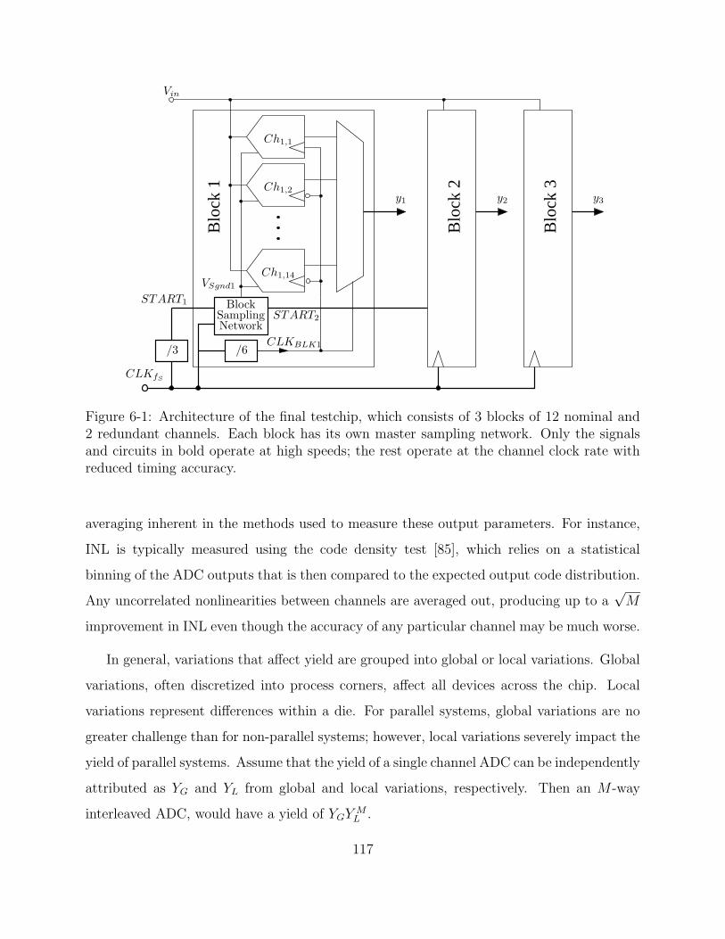
Blo
ck 2
Blo
ck 3
Blo
ck 1
y2 y3
SamplingNetwork
Block
/3 /6
Ch1,1
Ch1,2
CLKBLK1
VSgnd1
Vin
y1
START2
CLKfS
Ch1,14
START1
Figure 6-1: Architecture of the final testchip, which consists of 3 blocks of 12 nominal and2 redundant channels. Each block has its own master sampling network. Only the signalsand circuits in bold operate at high speeds; the rest operate at the channel clock rate withreduced timing accuracy.
averaging inherent in the methods used to measure these output parameters. For instance,
INL is typically measured using the code density test [85], which relies on a statistical
binning of the ADC outputs that is then compared to the expected output code distribution.
Any uncorrelated nonlinearities between channels are averaged out, producing up to a√
M
improvement in INL even though the accuracy of any particular channel may be much worse.
In general, variations that affect yield are grouped into global or local variations. Global
variations, often discretized into process corners, affect all devices across the chip. Local
variations represent differences within a die. For parallel systems, global variations are no
greater challenge than for non-parallel systems; however, local variations severely impact the
yield of parallel systems. Assume that the yield of a single channel ADC can be independently
attributed as YG and YL from global and local variations, respectively. Then an M -way
interleaved ADC, would have a yield of YGY ML .
117
Several ADC parameters are limited by local variation in any technology. For instance,
offset and static linearity are usually related to the matching of transistors, resistors, and/or
capacitors, where the matching is degraded by local variation between the active or passive
devices. In deep sub-micron CMOS, however, random dopant fluctuations have increased
local variations for transistors sized relative to the minimum feature size1 [119], meaning
that local variations are a greater concern, influencing not only the traditional parameters
but also digital delays, and preamplifier gain/bandwidth products.
Most local variations can be reduced at design time by increased area and/or power. The
variance of the threshold voltage in transistors, which impacts comparator offset and digital
propagation skews, is inversely proportional to the area [70]. The ratio error in capacitors,
which limits the static linearity, is also reduced with increasing capacitor size [67]. The
penalty for maintaining yield is significantly increased channel area and the power needed to
drive the greater capacitance, which negates much of the benefit from increasing parallelism.
This tradeoff of yield, matching, area, and power can be examined for the case of capacitor
array matching, which directly impacts the static linearity of a channel. Figure 6-2 plots
a set of waterfall curves of the yield for a given INL specification versus matching of the
unit capacitors within the array. To the right, matching degrades and the yield falls off
accordingly. In addition, as the number of parallel channels increases, the overall yield drops
rapidly for the same capacitor matching. To maintain the same yield level Y0 as the number
of channels increases from 1 to 36, the capacitor matching must improve from x1 to x36. This
corresponds to a 2.5× increase in capacitor area. Not only does this lead to a significant
increase in an already large die because the capacitors are the plurality of the channel area,
but it also leads to an increase in power consumption as larger capacitors require larger
switches and higher digital power consumption.
Another technique to improve linearity is to use calibration. The well known SAR cali-
bration procedure [31, 120] introduces a resistive calibration DAC coupled to the output of
the main DAC through a capacitor. This technique can fully calibrate any static linearity
1This does not only refer to minimum sized devices; instead, it refers to scaling a potentially larger devicebetween successive technology generations in proportion to the change in minimum feature size.
118

0.03 0.035 0.04 0.045 0.05 0.055 0.060
20
40
60
80
100
Yie
ld (
INL
<=
0.3
50)
(%)
σ0/C
0
3624
12
6
1
x36
x1
Num
ber
of c
hann
els
Figure 6-2: Yield versus capacitor array matching as number of channels increases. σ0/C0 isthe relative variation of the unit capacitors within the array. Yield is every channel havingan INL better than a 0.35 LSB specification.
and offset errors of the DAC and comparator, but it introduces a complexity and energy
overhead to every channel. In addition, some of the local variations that are more significant
in deep sub-micron CMOS, including digital propagation delays and timing skew, cannot
be fixed with this procedure. Calibration techniques can be designed for each of these error
sources, but this leads to rapidly increasing channel complexity with associated implications
on the design and test time of the ADC.
Instead, this work proposes the use of redundancy to mitigate yield loss from local vari-
ation in this parallel ADC. Memories have long used redundancy to correct failures in large
arrays [121] and, more recently, for column sense amplifier offset reduction [122]. Redun-
dancy is also not new to ADCs; redundant comparators have improved linearity in the flash
architecture [123, 124], but nothing as extensive as redundant channels. A simple example
demonstrates the advantage of redundancy. Assume a comparator occupying area A has an
offset that is normally distributed with standard deviation VOS0, and the yield constraint
119

requires the offset to be less than VOSmax (Fig. 6-3(a)). Then the total yield will be
YA = 1 − 2Φ
(
−VOSmax
VOS0
)
, (6.1)
where Φ(x) is the cumulative distribution function (CDF) of normal random variable x.
If now the available area is increased to 2A, both sizing and redundancy can be used
improve the yield. By doubling the transistors’ areas, the offset standard deviation decreases
by√
2 (the narrower curve in Fig. 6-3(a)) and the yield is
Ysizing = 1 − 2Φ
(
−√
2VOSmax
VOS0
)
. (6.2)
If instead there are two comparators of size A, and the one with the lowest absolute offset
is selected, the expected yield is
Yredundancy = 1 − 4Φ2
(
−VOSmax
VOS0
)
. (6.3)
These yields are plotted in Fig. 6-3(b) for various VOSmax/VOS0 ratios. As expected, both
sizing and redundancy improve yield compared to to the original comparator, but redundancy
always produces the higher yield.
Redundancy is most effective when it is applied at the highest level of parallelism of a
circuit or system. In this thesis, redundancy is applied at the level of the channel. This
does not require complete a priori knowledge of the impairments that will reduce yield;
instead, any of offset, digital timing delays, static linearity, dynamic linearity, or skew can
be measured during initial chip testing, and the best channels chosen. Redundancy is applied
to maintain the per channel requirements on par with those of the initial two prototypes.
While the offset requirements can be easily described with closed form solutions, as shown
above, other specifications (e.g., timing constraints or static linearity), have more complex
distributions that are not representable by simple equations. Instead, Monte Carlo behav-
ioral simulations are used to determine the effect of redundancy on these other parameters.
120
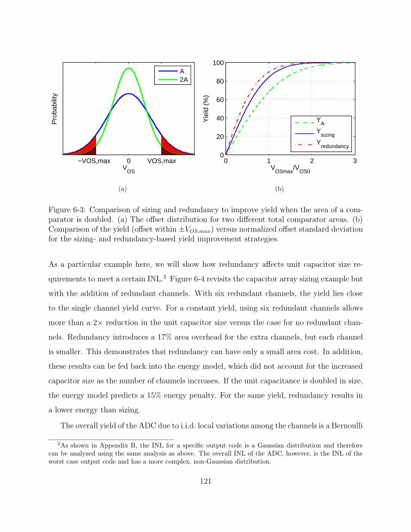
−VOS,max 0 VOS,max
Pro
babi
lity
VOS
A2A
(a)
0 1 2 30
20
40
60
80
100
VOSmax
/VOS0
Yie
ld (
%)
YA
Ysizing
Yredundancy
(b)
Figure 6-3: Comparison of sizing and redundancy to improve yield when the area of a com-parator is doubled. (a) The offset distribution for two different total comparator areas. (b)Comparison of the yield (offset within ±VOS,max) versus normalized offset standard deviationfor the sizing- and redundancy-based yield improvement strategies.
As a particular example here, we will show how redundancy affects unit capacitor size re-
quirements to meet a certain INL.2 Figure 6-4 revisits the capacitor array sizing example but
with the addition of redundant channels. With six redundant channels, the yield lies close
to the single channel yield curve. For a constant yield, using six redundant channels allows
more than a 2× reduction in the unit capacitor size versus the case for no redundant chan-
nels. Redundancy introduces a 17% area overhead for the extra channels, but each channel
is smaller. This demonstrates that redundancy can have only a small area cost. In addition,
these results can be fed back into the energy model, which did not account for the increased
capacitor size as the number of channels increases. If the unit capacitance is doubled in size,
the energy model predicts a 15% energy penalty. For the same yield, redundancy results in
a lower energy than sizing.
The overall yield of the ADC due to i.i.d. local variations among the channels is a Bernoulli
2As shown in Appendix B, the INL for a specific output code is a Gaussian distribution and thereforecan be analyzed using the same analysis as above. The overall INL of the ADC, however, is the INL of theworst case output code and has a more complex, non-Gaussian distribution.
121

0.03 0.04 0.05 0.06 0.070
20
40
60
80
100
σ0/C
0
Yie
ld (
INL
<=
0.3
50)
(%)
1 channel36 chs.36+136+336+6
Figure 6-4: Yield versus capacitor array matching as number of redundant channels increases.Also shown is the case for a single SAR ADC.
random process. If the probability of a single channel working is YL, then the probability of
at least M out of Mtotal = M + Mred channels is
Yred =
M+Mred∑
j=M
(
Mtotal
j
)
Y jL(1 − YL)Mtotal−j. (6.4)
Figure 6-5 shows the required channel yield YL as a function of the number of redundant
channels with 36 nominal channels. For a target yield of 95%, using six redundant channels
lowers the required per-channel yield from the stringent specification of 99.86% to the much
more relaxed 91.9%.
The translation of this relaxed specification into the channel design is heavily dependent
on the particular metrics that are important. If area is the primary concern, the capacitor
arrays, as the plurality of the channel area, are the appropriate choice for downsizing in
response to the relaxed yield, as described above. In the design of this chip, the capacitors
were made as small as permitted by the DRC and LVS tools but still achieved sufficient
matching that they are not the primary limitation on yield. Instead, the relaxed yield was
reserved for faults, such as residual timing skew and digital propagation delay errors, that
are both not as correctable and not fully modeled during the design phase.
122

0 2 4 6 8 10 120.8
0.85
0.9
0.95
1
Mred
Min
imum
YL
Yred
= 90%
95%99%99.9%
Figure 6-5: The required value of the per-channel yield YL to meet a target overall yield Yred
as a function of the number of redundant channels. The nominal number of channels M is36.
6.2 Block Details
6.2.1 Clock Generation and Block Redundancy
As discussed in Section 5.3.6, it is critical to distribute the minimum frequency clock to every
channel. As every channel requires (b + 1) internal clock periods for a conversion, M clocks
of frequency fch = (b + 1)fS/M separated in phase by
∆φ = 2π(b + 1)/M (6.5)
radians are required. Generating M phase shifted clocks leads to significant complexity in
the clock generation network; however, if k · (b + 1)/M = 1 for some integer k < M , then
channels i and i + k share the same clock phases. In particular, if M mod 6 ≡ 0, as in the
first two prototypes, then six channels share the same clock phase, and only six clocks must
be generated for the 36-way interleaved prototype. In general, for a b-bit time-interleaved
SAR ADC, clock generation requirements are minimized if M mod (b + 1) ≡ 0.
The redundancy analysis in the preceding section made the assumption that any M
channels could be chosen out of the total pool of M +Mred available channels; in this thesis,
123

this is called global redundancy. This is opposed, however, to each channel receiving a
single low frequency clock. One solution is to locate the redundant channels nearest to the
clock generation block so that they can receive, with minimal routing distance, either a full
speed fS clock or all 6 of the phase shifted fS/6 clocks. Still, this approach does not scale
well with larger numbers of redundant channels, and synchronization using the simple start
token passing scheme remains challenging. More sophisticated and potentially power hungry
synchronization methods would have to be developed for the redundant channels.
Another approach is to use block-level redundancy, where the channels are initially
grouped into blocks sharing common clock phases, and then redundant channels are al-
located to each block. Assume that each block has Mblock nominal channels and there are
Nblock = M/Mblock blocks. By allocating redundancy on a per block basis, instead of globally,
the yield is degraded for the same total number of redundant channels. The yield for a single
block is given by substituting the appropriate number of nominal and redundant channels
within a block into (6.4), which produces
Ysingle block =
Mblock+r∑
j=Mblock
(
Mblock+r
j
)
Y jL(1 − YL)Mblock+r−j. (6.6)
Here, Mblock+r = Mblock + Mred/Nblock is the total number of channels in a block. The total
number of redundant channels is now constrained to be a multiple of the number of blocks.
The total yield for block level redundancy is the product of (6.6) for each of the blocks
Yblock,red =
[
Mblock+r∑
j=Mblock
(
Mblock+r
j
)
Y jL(1 − YL)Mblock+r−j
]Nblock
, (6.7)
Redundancy is most effective when the block size is maximized (i.e., global redundancy).
Reconsidering (6.5) with M = 36 and b = 5, channels i and i + 6 share the same clock
phase as mentioned above, but channels i and i + 3 differ in clock phase by π radians. The
clock for channel i + 3 can therefore be derived from the clock for channel i using a digital
inverter. The fS/6 clock distributed to the channels should have a 50% duty cycle, which is
124
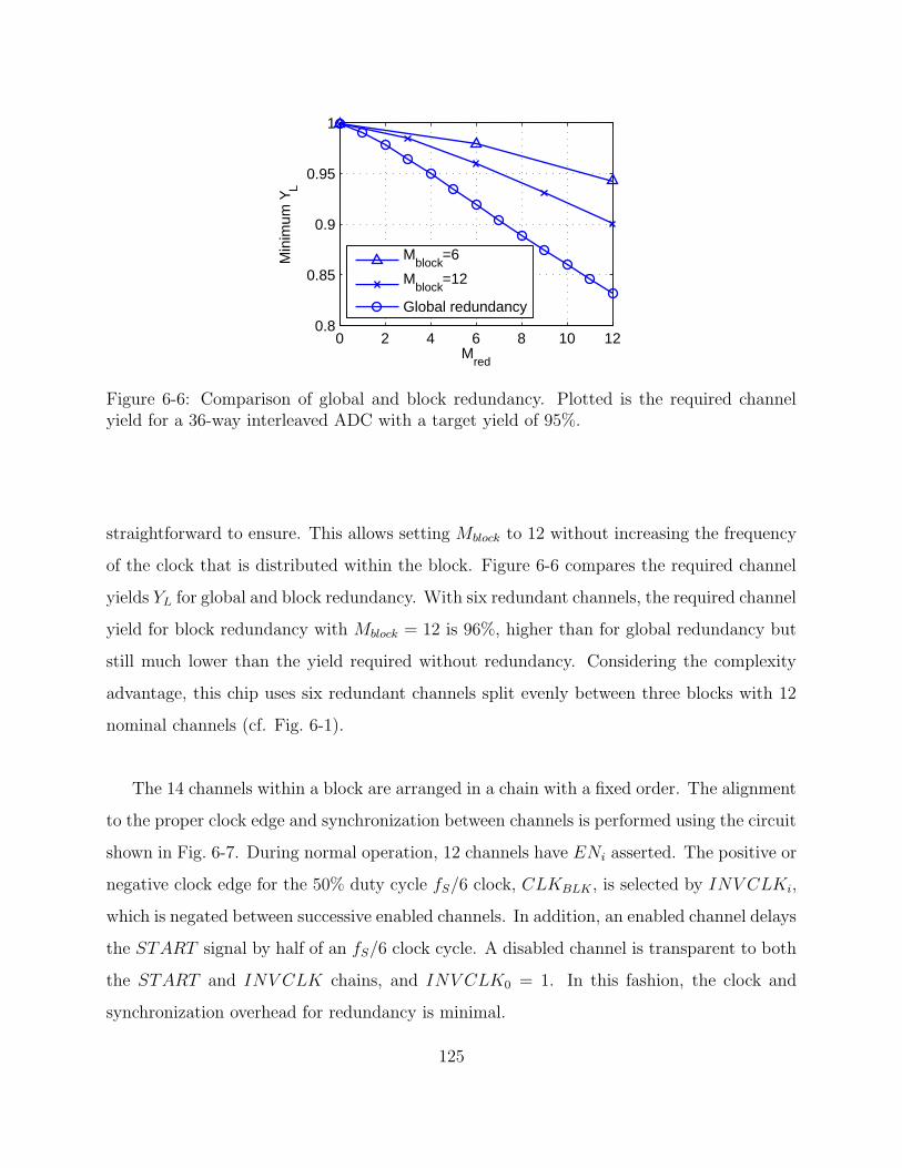
0 2 4 6 8 10 120.8
0.85
0.9
0.95
1
Mred
Min
imum
YL
Mblock
=6
Mblock
=12
Global redundancy
Figure 6-6: Comparison of global and block redundancy. Plotted is the required channelyield for a 36-way interleaved ADC with a target yield of 95%.
straightforward to ensure. This allows setting Mblock to 12 without increasing the frequency
of the clock that is distributed within the block. Figure 6-6 compares the required channel
yields YL for global and block redundancy. With six redundant channels, the required channel
yield for block redundancy with Mblock = 12 is 96%, higher than for global redundancy but
still much lower than the yield required without redundancy. Considering the complexity
advantage, this chip uses six redundant channels split evenly between three blocks with 12
nominal channels (cf. Fig. 6-1).
The 14 channels within a block are arranged in a chain with a fixed order. The alignment
to the proper clock edge and synchronization between channels is performed using the circuit
shown in Fig. 6-7. During normal operation, 12 channels have ENi asserted. The positive or
negative clock edge for the 50% duty cycle fS/6 clock, CLKBLK , is selected by INV CLKi,
which is negated between successive enabled channels. In addition, an enabled channel delays
the START signal by half of an fS/6 clock cycle. A disabled channel is transparent to both
the START and INV CLK chains, and INV CLK0 = 1. In this fashion, the clock and
synchronization overhead for redundancy is minimal.
125

1
0
1
01
0
D Q 1
0
D Q
1
0
1
0
STARTi+1
CLKi+1
STARTi+2
CLKBLK
STARTi
CLKi
EN
i
EN
i+1
ENi+1
INV CLKi INV CLKi+1
ENi
INV CLKi−1
Figure 6-7: Synchronization circuitry of the channels within a block. Successive enabledchannels align their clock, CLKi, to opposite edges of the fS/6 clock, CLKBLK , and delaythe START token by half a clock period.
6.2.2 Clock Partitioning
The fS/6 block clocks are designed to be distributed at the low core digital voltage in order to
further save clock distribution power. It is not possible to maintain precise timing alignments
with regards to skew and jitter at these lower voltages. Fortunately, the hierarchical top-
plate sampling network described below obviates the need for the channel clocks to have
precise timing. The precise clock is available at the master sampling switch (see Fig. 6-1),
and only one precise clock edge is sent from the master sampling network to a channel to
indicate the end of sampling. Sending one precise edge per conversion to each channel is
more efficient then distributing the precise clock to every channel; however, every channel
needs its own balanced path to the master sampling switch to receive this edge.
6.2.3 Output Mux
The output mux is the last major overhead for highly parallel ADCs. To ease PCB design
and speed of test equipment, the outputs of the three blocks are kept separate. The output
126

D Q
D Q1
01
0BUSR
BUSL
S Q
OEN1
OEN5
OEN8
OEN12
OEN10
OEN14
OEN2
OEN6
OEN3
OEN7
OEN9
OEN13
y<6:0>M2
R1
R2
CLKBLK
BUS
RL1
MUXL
MUXR
M1
Figure 6-8: Diagram of the block output mux. BUSL is shared by channels 1–7, and BUSR
is shared by channels 8–14. All datapath signals are 7 bits wide. Left/right select signalsMUXL and MUXR are dynamic nodes charge and discharged by the appropriate channeloutput enable signals, OENi.
mux combines the outputs of the 12 active channels within a block to a single bus operating
at fS/3. Within a block, the output mux is implemented as a shared bus. At the end of a
conversion, the channel drives its digital output onto the mux bus for one half of the fS/6
CLKBLK clock period. The mux bus driver is high impedance during the rest of a conversion.
The bus is sampled on both the rising and falling edges of CLKBLK . As each channel outputs
only when its data is ready, channels disabled due to redundancy are automatically skipped.
Routing the mux bus to all 14 channels within a block increases the parasitic capacitance
that must be driven by each channel. The bus is partitioned into two separate buses, serving
channels 1–7 and 8–14, respectively, as shown in the output mux schematic in Fig. 6-8. The
datapath within the mux is 7 bits wide to allow for digital offset correction down to 1/4
LSB. The set-reset latch L1 controls whether the left half of the mux (channels 1–7) or the
right half of the mux (8–14) is being sampled by the double edge triggered flip flop, formed
from the two single edge triggered flip flops R1 −R2 and two-input mux M2. L1 is set when
the output enable OENi of channels 1–3 is high, and it is reset when the output enable of
channels 8–10 is high. The output enables from channels 3 and 10 are required because it is
possible that channels 1–2 or 8–9 are disabled due to redundancy. The signals MUXL and
MUXR are routed along with the entire bus, which allows MN1–MN6 and MP1–MP6 to be
placed near the outputs of the appropriate channels, minimizing the capacitance that must
127

be driven by OENi. Partitioning of the output mux beyond the two halves is possible to
further reduce the bus capacitance but at increased depth of the mux tree.
6.3 Error Sources in Interleaved ADCs
Time-interleaved converters are subject to impairments not present in single-channel ADCs.
Mismatches in the offset, gain, and sampling instants produce distortion; an analysis of the
reduced SNDR and spurious tones can be found in [125]. A number of calibration procedures
have been proposed to reduce these mismatches. In [47], each of the channels is calibrated
to have equivalent gain and offset to a reference ADC. To enable background operation,
therefore not interrupting conversion, an extra high-speed channel is included. The digital
background calibration in [50] injects a pseudo-random sequence into the input of the ADC,
and then correlates to the same sequence to calibrate the gain and offset of the two time-
interleaved ADCs to each other. This technique increases the required input dynamic range
of the ADC to handle the dither signal added to the maximum analog input.
By using pseudo-random chopping (swapping the differential paths) of the input, the
calibration in [53] does not restrict the input dynamic range. This work further calibrates
for timing skew, as well as gain and offset mismatches. The skew compensation circuit uses
a 21-tap FIR filter that was implemented off chip.
When considering the low resolution of the ADC for this thesis, any calibration algorithm
must be carefully considered for its impact on the overall power consumption. For this pur-
pose, I will differentiate between correction and calibration circuits. The former necessarily
run continuously, actually correcting the digital outputs. These would be an adder, a mul-
tiplier, and a filter for offset, gain, and timing mismatches, respectively. The calibration
circuits determine the proper values for correction and can be run at a much reduced duty
cycle, sleeping after the values have been chosen. The minimal duty cycle limits the average
power consumption of the calibration loops, whereas the correction circuits directly impact
runtime power.
128

6.3.1 Hierarchical Top-Plate Multi-Sampling Network
Considering the above distinction, it is clear that offset is the cheapest impairment to correct
for digitally, with gain and timing mismatches each more power hungry. Thus, only digital
offset correction will be included as part of this thesis, as described in the previous chapter.
The gain mismatch is not a serious issue for this ADC as all channels share an identical
reference voltage, and the error due to capacitor mismatch, as confirmed by measurements,
is minimal. Timing mismatch, however, remains a pernicious problem. In the first two
implemented prototypes, it was demonstrated that by sharing a common sampling clock,
distortion from skew between six channels could be kept beneath the total noise power. This
is not expected to scale well to 36 channels. The die area is much larger, corresponding to
longer clock paths that are difficult to match. Also, as discussed in Section 5.3.6, distributing
the sampling clock to every channel in a balanced clock tree is very power hungry, with clock
distribution energy growing as M 3/2. A related problem to timing skew is phase variation in
the sampling networks between channels. Variation in the resistance and capacitance values
produces phase mismatch between channels, which for a single frequency input manifests
itself similarly to timing skew.
The combined effect of phase mismatch and timing skew is often modeled as adding
a timing offset tskew,i to every channel’s sampling ideal sampling point. Without better
knowledge of the timing skew a priori, tskew,i is chosen as a Gaussian random variable of
zero mean and standard deviation σskew. For the case of an M -way interleaved ADC the
maximum SNDR due to this timing skew is [126]
SNDR = 20 log
(
1
σskew2πfin
)
− 10 log
(
M − 1
M
)
. (6.8)
This second term is negligible for large M . The skew should be less than 16 psrms for a 5-bit
ADC sampling a 250 MHz input. This is difficult to achieve, particularly as routing length
and variation increase across a large die.
One approach that completely eliminates timing skew and phase mismatch is to precede
129

the time-interleaved ADC with a single high-speed active sample and hold, sampling at the
maximum sampling rate [57, 127]. Each channel only sees a held signal, and timing skew
does not produce any voltage error if sufficient settling time is used. The active S/H would
consume at least as much power as an input buffer, which as mentioned in Section 5.3.8
would significantly increase the overall ADC power consumption.
Gustavsson and Tan proposed a global passive sampling technique that can reduce the
skew related distortion by 10–20 dB [128,129], extending the technique introduced for double
sampling ADCs in [130]. They use a hierarchical top-plate sampling network, as shown in
Fig. 6-9. This sampling network is similar to earlier hierarchical sampling networks used
in multi-step ADC converters that sampled the input onto multiple capacitors at the same
time [131, 132]; the network in [128] makes two significant changes: placing the hierarchi-
cal network on the top-plate (signal-independent side) of the capacitor and separating the
sampling points of the capacitors for use in an interleaved ADC. Compared to the simple
sampling network in Fig. 5-5(a), the bottom plate switch connected to Vin is unchanged, but
the top plate switch is split into two series switches, a master switch SG shared among all the
channels, and a per-channel slave switch ST i. The timing diagram of the switches is shown
in Fig. 6-10. The sampling period for channel i occurs when both SG and ST i are closed,
with only one channel sampling at a time. The master switch SG opens first, defining the
sampling instant common to all channels, eliminating timing skew.
The presence of the parasitic capacitor Cpar, however, leads to some residual voltage error
due to timing skew between the per-channel slave switches. Defining the capacitor divider
ratio
a =Cpar
Cpar + CS
, (6.9)
the timing-skew related SNDR is [128]
SNDR = 20 log
(
1
σskew2πfin
)
− 10 log
(
M − 1
M
)
− 20 log(a). (6.10)
Compared to (6.8), the SNDR improves by 20 log(a).
130
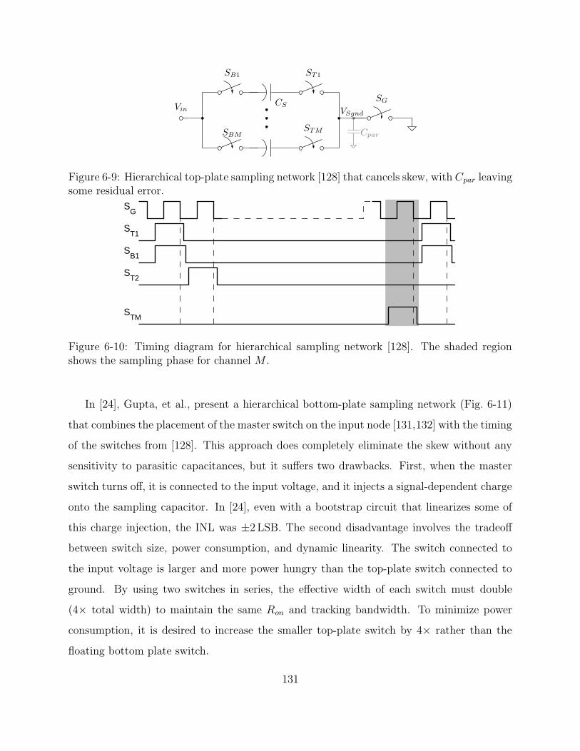
CS
Cpar
Vin VSgnd
SB1 ST1
SG
SBMSTM
Figure 6-9: Hierarchical top-plate sampling network [128] that cancels skew, with Cpar leavingsome residual error.
SG
ST1
SB1
ST2
STM
Figure 6-10: Timing diagram for hierarchical sampling network [128]. The shaded regionshows the sampling phase for channel M .
In [24], Gupta, et al., present a hierarchical bottom-plate sampling network (Fig. 6-11)
that combines the placement of the master switch on the input node [131,132] with the timing
of the switches from [128]. This approach does completely eliminate the skew without any
sensitivity to parasitic capacitances, but it suffers two drawbacks. First, when the master
switch turns off, it is connected to the input voltage, and it injects a signal-dependent charge
onto the sampling capacitor. In [24], even with a bootstrap circuit that linearizes some of
this charge injection, the INL was ±2 LSB. The second disadvantage involves the tradeoff
between switch size, power consumption, and dynamic linearity. The switch connected to
the input voltage is larger and more power hungry than the top-plate switch connected to
ground. By using two switches in series, the effective width of each switch must double
(4× total width) to maintain the same Ron and tracking bandwidth. To minimize power
consumption, it is desired to increase the smaller top-plate switch by 4× rather than the
floating bottom plate switch.
131
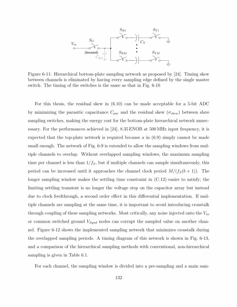
(boosted)
SB1 ST1
CS
SBM STM
Vin
SG
Cpar
Figure 6-11: Hierarchical bottom-plate sampling network as proposed by [24]. Timing skewbetween channels is eliminated by having every sampling edge defined by the single masterswitch. The timing of the switches is the same as that in Fig. 6-10
For this thesis, the residual skew in (6.10) can be made acceptable for a 5-bit ADC
by minimizing the parasitic capacitance Cpar and the residual skew (σskew) between slave
sampling switches, making the energy cost for the bottom-plate hierarchical network unnec-
essary. For the performances achieved in [24], 8.35 ENOB at 500 MHz input frequency, it is
expected that the top-plate network is required because a in (6.9) simply cannot be made
small enough. The network of Fig. 6-9 is extended to allow the sampling windows from mul-
tiple channels to overlap. Without overlapped sampling windows, the maximum sampling
time per channel is less than 1/fS, but if multiple channels can sample simultaneously, this
period can be increased until it approaches the channel clock period M/(fS(b + 1)). The
longer sampling window makes the settling time constraint in (C.12) easier to satisfy; the
limiting settling transient is no longer the voltage step on the capacitor array but instead
due to clock feedthrough, a second order effect in this differential implementation. If mul-
tiple channels are sampling at the same time, it is important to avoid introducing crosstalk
through coupling of these sampling networks. Most critically, any noise injected onto the Vin
or common switched ground VSgnd nodes can corrupt the sampled value on another chan-
nel. Figure 6-12 shows the implemented sampling network that minimizes crosstalk during
the overlapped sampling periods. A timing diagram of this network is shown in Fig. 6-13,
and a comparison of the hierarchical sampling methods with conventional, non-hierarchical
sampling is given in Table 6.1.
For each channel, the sampling window is divided into a pre-sampling and a main sam-
132

Cpar
VSgnd
SGVin
STi
STPi
SBi
Channel i
Figure 6-12: Implemented multi-sampling network for use with overlapped sampling win-dows. The additional top-plate pre-sampling switch, STPi avoids crosstalk on VSgnd, and SBi
is turned on with a slow ramp signal.
SG
STPi
STi
SBi
Figure 6-13: Timing diagram of the hierarchical sampling network with slow turn-on bottomplate switch drive and overlapped sampling windows with minimal crosstalk.
Table 6.1: Comparison of interleaved sampling methods
Method
Globalsamplingswitch
location
SkewSwitchload
Signaldependent
chargeinjection
Overlappedsamplingwindows
Conventional None Large Small No No[128] Top-plate Small Medium No No[24] Bottom-plate None Large Yes No
Proposed Top-plate Small Medium No Yes
pling phase. An additional top plate switch STPi is added to every channel that is closed
during pre-sampling, connecting the top-plate to ground directly, as opposed to through SG.
During the main sampling phase for channel i, switch ST i is closed and STPi is open, con-
necting the top-plate to VSgnd. Only one channel at a time is connected to VSgnd, minimizing
133

0 2 4 6 8 10 12−800
−600
−400
−200
0
200
Time (ns)
Inje
cted
cur
rent
(µA
)
Fast turn−onSlow turn−on
Figure 6-14: Simulation showing the current injected into the input node from the turn-on ofthe bottom switch when it is driven quickly to VDDS and with the implemented slow turn-ongate drive. The slow turn-on reduces the peak current by more than 8.5×.
crosstalk on this node, and the sampling instant is still defined by the opening of SG to
reduce skew. The input signal is driven with a 50 Ω source, so any current injected onto
the input node at the onset of sampling will be converted to a voltage by this resistance,
potentially corrupting charge in another channel. The bottom-plate switch SBi is turned
on with a slow ramp (Fig. 6-13) to the core VDDD, and is held there in a weakly on state.
During main sampling, the top-plate switch is connected to VDDS and is strongly turned on.
As shown in the simulations in Fig. 6-14, driving the top-plate switch with this slow turn-on
during pre-sampling reduces the current kickback noise onto the input node by 8.5×, making
the resultant voltage error less than an LSB. The kickback noise is sufficiently low that no
measures are taken to further align the start of sampling away from critical edges of the
other sampling channels. Simulations show that the slow ramp on the bottom plate switch
could continue to VDDS (without stopping at VDDD) without an increase in kickback noise
for a possible simplified implementation.
Figure 6-15 shows the circuit details of the channel sampling logic, used to drive the
switches in Fig. 6-12. The rising edge of LSAMP triggers pre-sampling and strongly turns on
the pre-sampling top-plate switch via STP . The bottom plate switch is driven using the slow
turn-on switch drive composed of MP1–MP3 and MN1–MN2. By making MP1–MP2 relatively
134

CL
R
QDR1
LS1
LS2
ST
ST
STPRESETBC
LSAMP SBMP2
MN2
MP3
MP1
MN1
CHSAMP
CHSAMP
STP
VDDSVDDD
Figure 6-15: The channel sampling logic to drive the bottom plate switch SB, and the pre-sampling and main sampling switches STP and ST . All blocks in bold are powered off of thesampling voltage VDDS , while the remaining blocks are connected to VDDD. Level shiftersLS1–LS2 are used to convert from the lower to higher voltage domains.
weak, output voltage SB is slowly driven to VDDD at the start of pre-sampling. When the
channel receives CHSAMP from the block sampling network (see Fig. 6-16), it turns on the
main top plate switch ST , connects SB to VDDS via MP3, and turns off the pre-sampling top-
plate switch by resetting R1. Finally, on the falling edge of CHSAMP , all sampling switches
are opened. Level shifters are inserted to convert between the core digital voltage VDDD and
the sampling switch voltage VDDS.
The signals that produce the falling edge of ST i and SBi are derived from the falling
edge of the master switch signal SG using logic connected to the higher voltage sampling
supply VDDS. As digital delay variations increase at lower voltages, connecting this signal
path to the higher voltage reduces the skew between the slave switches, σskew, and improves
the SNDR (6.10) at only a small power overhead.
To reduce the distance between the master sampling switch and the channels and to
minimize the parasitic capacitance CPar in Fig. 6-12, three master sampling switches are
used, one for each block. This introduces an extra source of skew between the blocks;
however, the parasitic capacitance is now less than 1/3 of its value with a single master
switch, reducing a in (6.9), and improving the cancellation of intra-block skew. The precise
full speed sampling clock is distributed to all three of these master switches in a balanced
layout.
135

1
0
1
0
D Q
CL
R
D QC
LR
A1A1
SG
BLKSAMP
Gi
EN
i+1
CHSAMP,i+1Gi
EN
i
CHSAMP,i
BLKSAMP BLKSAMP
pGi+2
VSgnd
pGi pGi+1
Figure 6-16: Simplified schematic of the per-block master sampling network. SG is themaster top-plate sampling switch. The sampling clock BLKSAMP is gated by Gi to generatethe per-channel main sampling window CHSAMP,i.
Within each block, the master sampling network includes the master sampling switch
and the logic to distribute the end of sampling signal to each channel. It operates at the
higher sampling voltage VDDS to minimize skew, jitter, and maximize the overdrive of the
sampling switches. A simplified schematic is shown in Fig. 6-16. BLKSAMP is the fS/3
master sampling clock derived from the fS full speed sampling clock distributed to all three
block sampling networks, and it directly drives the global sampling switch SG. The AND
gates A1 mask this signal to generate CHSAMP,i, which is sent only to the one channel that
is in its main sampling phase. The falling edge of CHSAMP,i opens the per-channel top plate
switch (Fig. 6-15). The gating signal Gi is generated with a shift register, similar to that
used for the channel synchronization (cf. Fig. 6-7), that is transparent for disabled (due to
redundancy) channels. The timing of Gi is controlled to ensure that it transitions low while
BLKSAMP is low to avoid any glitches on CHSAMP,i.
136

6.4 Channel Circuit Details
The basic channel structure is similar to the previous two chips but with no analog/digital
timing adjustment, either in the form of self-timing or with a VDL.3 The split capacitor
array is used, with the two differential capacitor arrays having swapped subarrays (see Ap-
pendix A). The sizes of array switches, buffer chains driving the switches, and transistors in
the comparator were initially taken from the outputs of the energy model, with only minor
adjustments made after transistor-level simulations. The following sections discuss differ-
ences in the channel circuitry compared to the prior chips. These include a half-rate SAR
controller, a DAC-biased preamplifier, and the circuits to implement the channel-specific
parts of the output mux.
6.4.1 DAC-biased Preamplifiers
The duty-cycled preamplifier of Fig. 3-8(b) is enhanced by replacing the fixed current source
with a DAC that can be varied on a per-channel basis. This allows post fabrication cor-
rection for mismatch in the bias network or PFET load transistors that bias an individual
preamplifier out of its desired operating region, which in turn leads to severe offset or lin-
earity degradation. In addition, for channels that have a very low latch offset voltage, the
required gain in the preamplifiers is minimal. The bandwidth of the preamplifier is set by
the resistance of the PFET loads and load capacitance, both of which are relatively inde-
pendent of the bias current. By decreasing the preamplifier bias currents in channels with
small offsets, the power savings are achieved without sacrificing preamplifier speed or static
linearity. For highly parallel systems, the average power can be reduced by allocating power
on a per-channel basis; this is an additive effect with redundancy. The price is additional
per-channel complexity and a longer test time. If implemented, the potential built-in self
test (BIST) described in Section 6.6.4 could also dynamically bias the preamplifiers in re-
sponse to measured chip performance. For the majority of testing, every preamplifier was
3Section 5.4.3 presented the energy model analysis of the VDL, showing that it does not produce energysavings for this highly parallel converter
137
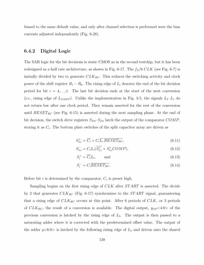
biased to the same default value, and only after channel selection is performed were the bias
currents adjusted independently (Fig. 6-28).
6.4.2 Digital Logic
The SAR logic for the bit decisions is static CMOS as in the second testchip, but it has been
redesigned as a half rate architecture, as shown in Fig. 6-17. The fS/6 CLK (see Fig. 6-7) is
initially divided by two to generate CLKBC . This reduces the switching activity and clock
power of the shift register R1 −R6. The rising edge of Li denotes the end of the bit decision
period for bit i = 4,. . .,1. The last bit decision ends at the start of the next conversion
(i.e., rising edge of LSAMP ). Unlike the implementation in Fig. 3-5, the signals L5–L1 do
not return low after one clock period. They remain asserted for the rest of the conversion
until RESETBC (see Fig. 6-15) is asserted during the next sampling phase. At the end of
bit decision, the switch drive registers SD4–SD1 latch the output of the comparator COMP ,
storing it as Ci. The bottom plate switches of the split capacitor array are driven as
S+5,i = Ci + CiLi RESETBC , (6.11)
S−5,i = CiLi(S
+5,i + S+
5,iCOMP ), (6.12)
S+i = CiLi, and (6.13)
S−i = CiRESETBC . (6.14)
Before bit i is determined by the comparator, Ci is preset high.
Sampling begins on the first rising edge of CLK after START is asserted. The divide
by 2 that generates CLKBC (Fig. 6-17) synchronizes to the START signal, guaranteeing
that a rising edge of CLKBC occurs at this point. After 6 periods of CLK, or 3 periods
of CLKBC , the result of a conversion is available. The digital output, yOS<4:0> of the
previous conversion is latched by the rising edge of L5. The output is then passed to a
saturating adder where it is corrected with the predetermined offset value. The output of
the adder y<6:0> is latched by the following rising edge of L5 and driven onto the shared
138
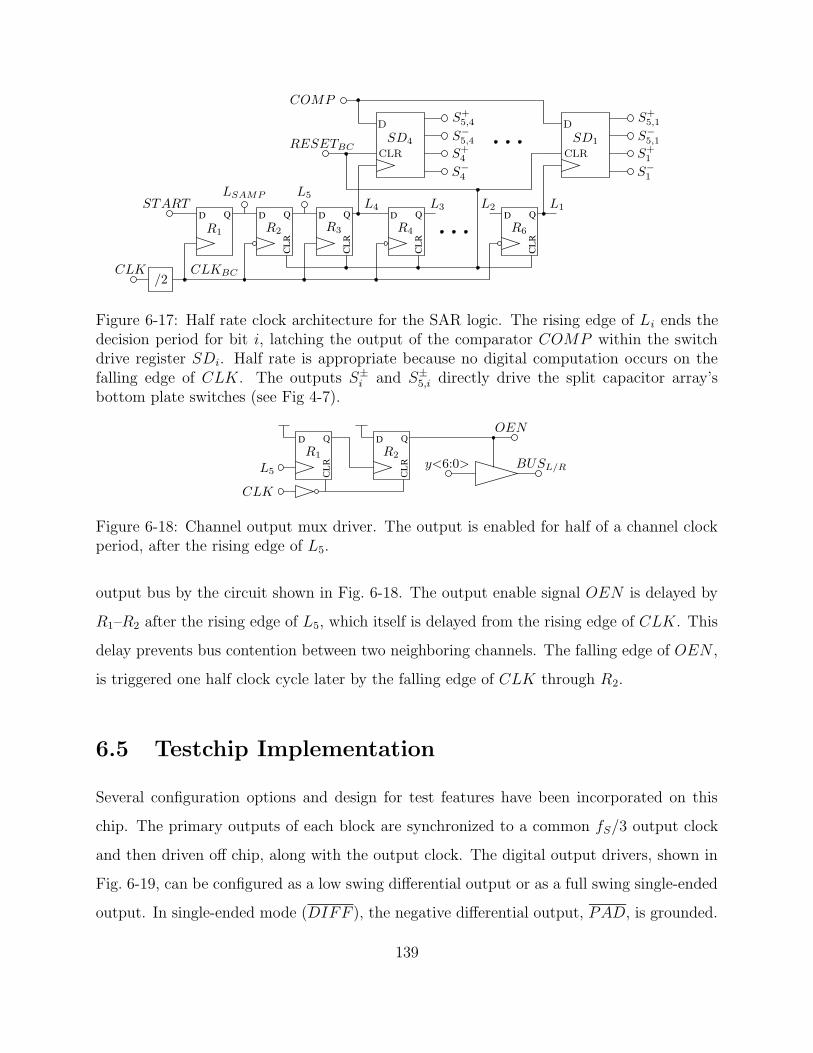
CLR
QD
CLR
QDQD
CLR
QD
CLR
QDR3R2R1 R4 R6
/2
SD4
D
CLR
S−
4
S+4
S−
5,4
S+5,4
SD1
D
CLR
S−
1
S+1
S−
5,1
S+5,1
L4
L5LSAMPL3 L2 L1START
CLK CLKBC
COMP
RESETBC
Figure 6-17: Half rate clock architecture for the SAR logic. The rising edge of Li ends thedecision period for bit i, latching the output of the comparator COMP within the switchdrive register SDi. Half rate is appropriate because no digital computation occurs on thefalling edge of CLK. The outputs S±
i and S±5,i directly drive the split capacitor array’s
bottom plate switches (see Fig 4-7).C
LR
QD
CL
R
QDR2R1
y<6:0>
OEN
CLK
L5BUSL/R
Figure 6-18: Channel output mux driver. The output is enabled for half of a channel clockperiod, after the rising edge of L5.
output bus by the circuit shown in Fig. 6-18. The output enable signal OEN is delayed by
R1–R2 after the rising edge of L5, which itself is delayed from the rising edge of CLK. This
delay prevents bus contention between two neighboring channels. The falling edge of OEN ,
is triggered one half clock cycle later by the falling edge of CLK through R2.
6.5 Testchip Implementation
Several configuration options and design for test features have been incorporated on this
chip. The primary outputs of each block are synchronized to a common fS/3 output clock
and then driven off chip, along with the output clock. The digital output drivers, shown in
Fig. 6-19, can be configured as a low swing differential output or as a full swing single-ended
output. In single-ended mode (DIFF ), the negative differential output, PAD, is grounded.
139
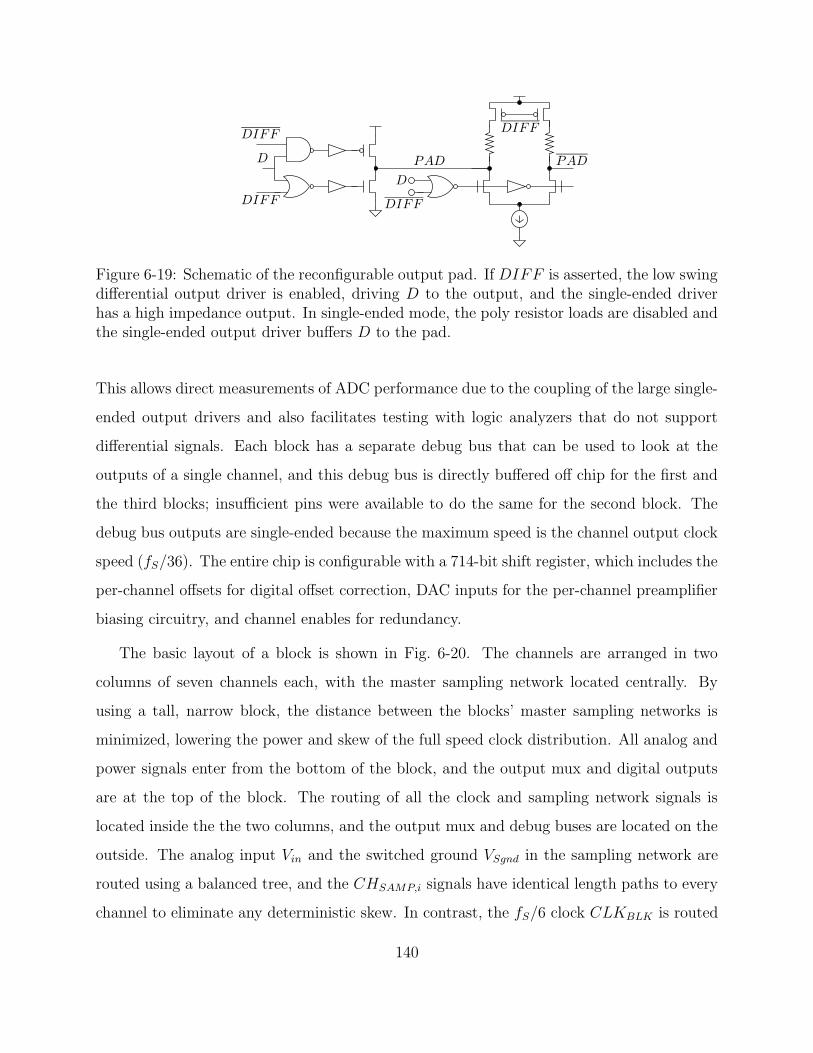
D
DIFF
DIFF
DIFF
DIFF
D
PAD PAD
Figure 6-19: Schematic of the reconfigurable output pad. If DIFF is asserted, the low swingdifferential output driver is enabled, driving D to the output, and the single-ended driverhas a high impedance output. In single-ended mode, the poly resistor loads are disabled andthe single-ended output driver buffers D to the pad.
This allows direct measurements of ADC performance due to the coupling of the large single-
ended output drivers and also facilitates testing with logic analyzers that do not support
differential signals. Each block has a separate debug bus that can be used to look at the
outputs of a single channel, and this debug bus is directly buffered off chip for the first and
the third blocks; insufficient pins were available to do the same for the second block. The
debug bus outputs are single-ended because the maximum speed is the channel output clock
speed (fS/36). The entire chip is configurable with a 714-bit shift register, which includes the
per-channel offsets for digital offset correction, DAC inputs for the per-channel preamplifier
biasing circuitry, and channel enables for redundancy.
The basic layout of a block is shown in Fig. 6-20. The channels are arranged in two
columns of seven channels each, with the master sampling network located centrally. By
using a tall, narrow block, the distance between the blocks’ master sampling networks is
minimized, lowering the power and skew of the full speed clock distribution. All analog and
power signals enter from the bottom of the block, and the output mux and digital outputs
are at the top of the block. The routing of all the clock and sampling network signals is
located inside the the two columns, and the output mux and debug buses are located on the
outside. The analog input Vin and the switched ground VSgnd in the sampling network are
routed using a balanced tree, and the CHSAMP,i signals have identical length paths to every
channel to eliminate any deterministic skew. In contrast, the fS/6 clock CLKBLK is routed
140
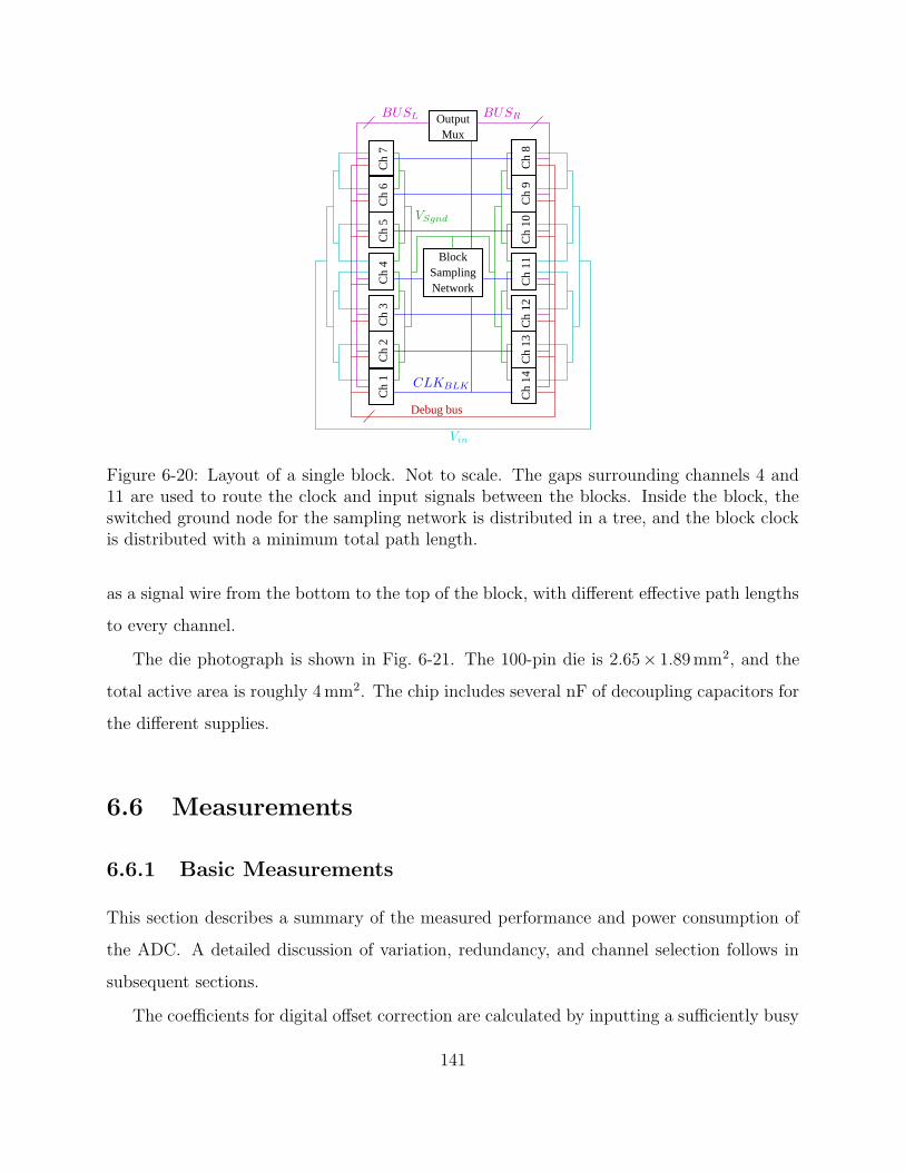
OutputMux
SamplingNetwork
Block
Ch
14C
h 13
Ch
12C
h 11
Ch
10C
h 9
Ch
8
Ch
1C
h 2
Ch
3C
h 4
Ch
5C
h 6
Ch
7
Debug bus
Vin
BUSR
VSgnd
CLKBLK
BUSL
Figure 6-20: Layout of a single block. Not to scale. The gaps surrounding channels 4 and11 are used to route the clock and input signals between the blocks. Inside the block, theswitched ground node for the sampling network is distributed in a tree, and the block clockis distributed with a minimum total path length.
as a signal wire from the bottom to the top of the block, with different effective path lengths
to every channel.
The die photograph is shown in Fig. 6-21. The 100-pin die is 2.65× 1.89 mm2, and the
total active area is roughly 4 mm2. The chip includes several nF of decoupling capacitors for
the different supplies.
6.6 Measurements
6.6.1 Basic Measurements
This section describes a summary of the measured performance and power consumption of
the ADC. A detailed discussion of variation, redundancy, and channel selection follows in
subsequent sections.
The coefficients for digital offset correction are calculated by inputting a sufficiently busy
141
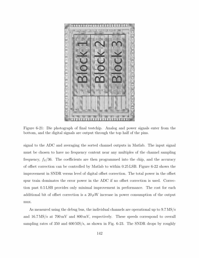
Figure 6-21: Die photograph of final testchip. Analog and power signals enter from thebottom, and the digital signals are output through the top half of the pins.
signal to the ADC and averaging the sorted channel outputs in Matlab. The input signal
must be chosen to have no frequency content near any multiples of the channel sampling
frequency, fS/36. The coefficients are then programmed into the chip, and the accuracy
of offset correction can be controlled by Matlab to within 0.25 LSB. Figure 6-22 shows the
improvement in SNDR versus level of digital offset correction. The total power in the offset
spur train dominates the error power in the ADC if no offset correction is used. Correc-
tion past 0.5 LSB provides only minimal improvement in performance. The cost for each
additional bit of offset correction is a 20µW increase in power consumption of the output
mux.
As measured using the debug bus, the individual channels are operational up to 9.7 MS/s
and 16.7 MS/s at 700 mV and 800 mV, respectively. These speeds correspond to overall
sampling rates of 350 and 600 MS/s, as shown in Fig. 6-23. The SNDR drops by roughly
142

None 1 0.5 0.2525
30
35
40
45
Offset Correction (LSB)
dB
SNDROffset train power
Figure 6-22: ADC performance as the level of offset correction is varied.
4 dB for a Nyquist input (relative to the interleaved sampling rate) as the overall sampling
frequency increases from 100 to 600 MHz.
Interleaved measurements are limited to below 400 MS/s operation because of a failure in
the output mux. The capacitance on the shared bus (BUSL/R in Fig. 6-8) was higher than
the mux bus driver (Fig. 6-18) was designed to drive. This failure can be partially corrected
at test time by adjusting various power supplies to indirectly move clock edges, but this
only extends the operating frequency up to 400 MHz. A schematic showing the critical paths
and relevant supplies is shown in Fig. 6-24. A separate supply, VDDC , was pinned out for
the clock distribution, which allows somewhat independent control of the clock edges. The
channel output registers R1 and R2 are clocked by L5 (Fig. 6-17) and CLKi (Fig. 6-7), both
of which are driven by VDDD powered blocks. The block clock ,CLKBLK , is powered by
VDDC . Register R5 is used to synchronize the outputs of all three blocks to a common fS/3
output clock, OCLK, in order to simplify testing with a logic analyzer. Both R5 and OCLK
are powered by the I/O power supply VDDIO.
In simulations, the bus driver is capable of driving a 200 fF load in 1.6 ns, well below the
approximately 4 ns (at 500 MS/s) available between the rising edges of L5 and CLKBLK .
Parasitic extraction predicted a wiring capacitance of 130 fF, making the design of this
block relatively conservative, but measurements indicate setup time failures of R3/R4 as the
143

0 2 4 6
x 108
0
5
10
15
20
25
30
35
fS (MHz)
SN
DR
(dB
)
0.7 V, low fin
0.8 V, low fin
0.7 V, Nyquist0.8 V, Nyquist
Figure 6-23: Individual channel performance for low frequency and Nyquist inputs. Theplotted sampling rate refers to the interleaved sampling rate; the channel is sampling atfS/36.
CL
R
QD
CL
R
QD
1
0
D Q
D Q
1
0
D Q
per channel
R2R1
BUSR
LS1
R5
L5y
M1
R3
R4
BUS
BUSL
M2
OCLKCLKBLK
CLKi
Figure 6-24: Schematic of the path from the output of a single channel to the pad drivers(output of R5). Signals that are not relevant to the critical paths are omitted. The twopotential errors are a violation of the setup time of R3/4, or a violation of the setup timeof R5. Clocks CLKi, CLKBLK , and OCLK are powered by VDDD, VDDC , and VDDIO,respectively.
144

100
102
10
15
20
25
30
35
40
45
fin
(MHz)
dB
SNDRTHDP
OSG
GS
(a)
0 50 100−80
−60
−40
−20
0
H7
H3
GGGG GGGGG O
frequency (MHz)
dB
(b)
Figure 6-25: Dynamic performance of the ADC at 250 MS/s, showing (a) the SNDR versusinput frequency and (b) an FFT of a near Nyquist input. The labeled dominant spursare harmonic distortion (Hi), multiples of the channel sampling frequency (O), or mixingproducts of the channel sampling frequency and the input (G).
sampling frequency increases beyond 300 MHz for VDDD = 0.8V . By lowering VDDC relative
to VDDD, the clock of R3 and R4 is delayed, but this leads to setup time violations of R5. The
I/O power supply can be lowered to delay the edge of OCLK, but only a limited reduction
in VDDIO is possible before the output drivers operating upwards of 150 MHz begin to fail.
Careful control of VDDD, VDDC , and VDDIO, has extended the operating frequency up to
400 MHz, but beyond that, output mux failures cannot be completely eliminated and the
ADC performance degrades severely.
At 800 mV core voltage, 1.2 V sampling voltage, and 250 MHz sampling frequency, the
dynamic performance is plotted versus input frequency in Fig. 6-25(a). The individual error
contributions from harmonic distortion (THD), total power in the offset train (POS), and
the total power in the mixing products from gain mismatch and skew (PGS) are plotted
separately. The frequency independent part of PGS is from gain mismatch, whereas its
degradation at high frequencies is due to timing skew. An FFT of a Nyquist input tone is
shown in Fig. 6-25(b). The ADC achieves an ENOB of 4.42 at Nyquist while consuming total
145
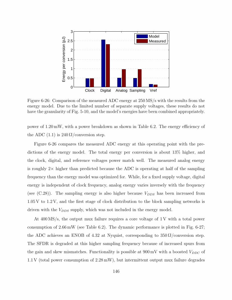
Clock Digital Analog Sampling Vref0
0.5
1
1.5
2
2.5
3
Ene
rgy
per
conv
ersi
on (
pJ)
ModelMeasured
Figure 6-26: Comparison of the measured ADC energy at 250 MS/s with the results from theenergy model. Due to the limited number of separate supply voltages, these results do nothave the granularity of Fig. 5-10, and the model’s energies have been combined appropriately.
power of 1.20 mW, with a power breakdown as shown in Table 6.2. The energy efficiency of
the ADC (1.1) is 240 fJ/conversion step.
Figure 6-26 compares the measured ADC energy at this operating point with the pre-
dictions of the energy model. The total energy per conversion is about 13% higher, and
the clock, digital, and reference voltages power match well. The measured analog energy
is roughly 2× higher than predicted because the ADC is operating at half of the sampling
frequency than the energy model was optimized for. While, for a fixed supply voltage, digital
energy is independent of clock frequency, analog energy varies inversely with the frequency
(see (C.28)). The sampling energy is also higher because VDDS has been increased from
1.05 V to 1.2 V, and the first stage of clock distribution to the block sampling networks is
driven with the VDDS supply, which was not included in the energy model.
At 400 MS/s, the output mux failure requires a core voltage of 1 V with a total power
consumption of 2.66 mW (see Table 6.2). The dynamic performance is plotted in Fig. 6-27;
the ADC achieves an ENOB of 4.32 at Nyquist, corresponding to 350 fJ/conversion step.
The SFDR is degraded at this higher sampling frequency because of increased spurs from
the gain and skew mismatches. Functionality is possible at 900 mV with a boosted VDDC of
1.1 V (total power consumption of 2.28 mW), but intermittent output mux failure degrades
146

100
102
10
15
20
25
30
35
40
45
fin
(MHz)
dB
SNDRTHDP
OSG
GS
(a)
0 50 100 150 200−80
−60
−40
−20
0
H3
GG G GGGG O
frequency (MHz)
dB
(b)
Figure 6-27: Dynamic performance of the ADC at 400 MS/s, showing (a) the SNDR versusinput frequency and (b) an FFT of a 190 MHz input.
Table 6.2: Power breakdown of ADC
Supply DescriptionVoltage Current Voltage Current
fS = 250 MS/s fS = 400 MS/sVDDD Core digital 800 mV 720µA 1.0 V 1.39 mAVDDA Core analog 800 mV 300µA 1.0 V 600µAVDDC Clock 800 mV 145µA 1.0 V 250µAVDDS Sampling 1.2 V 200µA 1.2 V 310µAVREF Reference 350 mV 89µA 350 mV 140µA
the Nyquist ENOB to 3.96. These output mux failures can produce outputs that are off by
several bits and therefore the ADC’s BER [71] increases significantly.
The per-channel preamplifier biasing has also been tested, as shown in Fig. 6-28. As
PREI, the digital code to the DAC, increases, the gains of the preamplifiers also increase,
reducing the measured offset voltage. For small PREI, the channel SNDR degrades because
the preamplifiers are effectively attenuating the input below the offset of the latch. As the
current gets too large, the PFET preamplifier loads enter saturation, and the input devices
enter triode, severely degrading the gain, offset, and SNDR. The preamplifier currents can be
chosen on a per-channel basis to meet the overall offset and SNDR specification. Optimizing
147

0 2 4 6−5
0
5
PREI
OS
(LS
B)
(a)
0 2 4 615
20
25
30
PREI
SN
DR
(dB
)
(b)
Figure 6-28: Measured channel (a) offsets and (b) SNDR as a function of the programmablepreamplifier bias current. Curves for 36 channels are overlayed.
each preamplifier bias current provides current savings at constant overall performance, but
the measured savings is only 80µA. This is roughly 20% of the current drawn from the
analog supply but only a small fraction of the overall power. Per-channel power distribution
may be more effective for systems that have a larger analog power contribution, but it must
be weighed against the additional complexity and test time.
6.6.2 Local Variation
Channel selection for redundancy begins with a measurement of the variation across a chip.
The raw measurements are converted into the set of metrics INL, DNL, SNDRL, SNDRH,
THDH offset, gain, timing skew. The subscript “L” denotes low frequency performance, and
the subscript “H” denotes Nyquist input. This input frequency is based on the overall inter-
leaved sampling rate, not the sampling rate of an individual channel. This set of parameters
requires only two measurements per channel, one with a low frequency sinusoidal input, and
one with a high frequency input. The interleaved outputs of the ADC include measurements
from 36 channels at the same time, and only four total measurements are needed to generate
148

0 5 10 15 20 25 30 35 40
0.2
0.4
INL
(LS
B)
0 5 10 15 20 25 30 35 40−2
0
2
OS
(LS
B)
0 5 10 15 20 25 30 35 40
−100
0
100
Ske
w (
ps)
Channel #
Figure 6-29: Variation of INL, offset, and skew across the 42 channels on a die.
all the data: two for channels 1–36, and two for channels 1–30 and 37–42.
With the exception of timing skew, all of the parameters can be based on looking at
the outputs of a single channel. Timing skew is extracted from the Nyquist input test by
individually sine fitting the output of each channel. The channel phases are unfolded to a
monotonically increasing sequence of phases that are then converted into time delays with
the known input frequency (∆t = ∆φ/(2πfin)). Timing skew is the variation between the
measured and ideal channel sampling instants. Without an accurate timing base, the ideal
sampling instant is set such that the average timing skew of the first 30 channels measured
in that run is 0.
Figure 6-29 shows a typical variation of some of these metrics across the 42 channels on
a single chip. Unless explicitly mentioned otherwise, all channel variation and redundancy
measurements are performed at VDDD = 0.9 V and fS = 250 MS/s. The total level of
variation does limit the yield, but the structure of the variation is critical to the yield
improvement achievable through redundancy. Redundancy is most effective when correcting
149

0 5 10 15 20 25 30 35 40
−0.1
0
0.1
INL
(LS
B)
0 5 10 15 20 25 30 35 40
−1
0
1
VO
S (
LSB
)
0 5 10 15 20 25 30 35 400.95
1
1.05
Channel #
Gai
n (N
orm
aliz
ed)
Figure 6-30: Average of the static parameters (INL, offset, gain) for each channel across allmeasured dies. The dashed lines indicate the 5th and 95th percentiles of the parameters crossall measured channels. The INL measurement at top is the INL of the MSB transition, notthe overall INL for the channel. The measurements on all chips were performed at 250 MS/swith a 0.9 V core voltage.
“white” variations, where every channel is completely independent. If the same channels
are bad on every chip (i.e., systematic variation), it is an implementation-induced error that
can be corrected through improved layout. Alternatively, if the bad channels are clustered
within a single block (e.g., if the block sampling network is defective), then the two redundant
channels will be insufficient to correct all the errors.
Systematic variation is determined by averaging the parameters of each channel across all
the dies, as shown in Figures 6-30 and 6-31. As only 24 chips were available for measurements,
this is only an estimate of systematic variation, and this same caveat applies to any other
general conclusions about variation and yield. Where present, the dashed lines indicate the
5th and 95th percentiles across all channels. The redundant channel selection procedure
presented in Section 6.6.3 typically replaces channels that fall outside of these bounds. In
150

0 5 10 15 20 25 30 35 4020
30
40
50
dB (
low
−f in
)
SNDRTHD
0 5 10 15 20 25 30 35 4020
30
40
50
dB (
Nyq
uist
)
SNDRTHD
0 5 10 15 20 25 30 35 40
−20
0
20
Ske
w (
ps)
Channel #
Figure 6-31: Average of the dynamic parameters for each channel across all measured dies.With the exception of channel 3 at the high input frequency, the SNDR of all channelsexhibits no systematic variation, as is it dominated by quantization noise and, at highfrequencies, jitter.
general, the level of systematic variation is less than the level of random variation. A few of
these plots, however, require further consideration.
The offset voltage displays a clear structure where channels 1, 4, . . . , 40 have a more
negative offset voltage than the rest of the channels. This is a result of systematic block
variation, as all of these channels are in block 1. The first block has an average offset
voltage 0.64 LSB less than the other two blocks. While the layouts of blocks 2 and 3 are
identical, the first block has an added circuit to generate the START signals. This circuit
asymmetrically couples to the differential switched ground nodes in the hierarchical sampling
network, causing the systematic block offset.
The gains show a significant bowing, with increased gain for the channels in the middle
that are located towards the top of the die. The reference voltage supply is routed from the
bottom of the die, and the increased IR drop seen by the upper channels attenuates VREF ,
151

0 5 10 15 20 25 30 35 4020
30
40
50
dB (
Nyq
uist
)
SNDRTHD
Figure 6-32: Systematic variation of SNDR and THD with the debug bus turned off. Asshown, the SNDR drop in channel 4 is eliminated.
which is equivalent to an amplification of the input signal.
While the SNDR and THD for low frequency inputs shows almost no variation, channel 4,
the second channel in block 1, shows clearly degraded THD and SNDR with a Nyquist input.
While not all chips exhibit this degradation, enough do that channel 4 must be replaced with
a redundant channel on a disproportionate number of chips. This error is due to coupling
from the first block’s debug bus onto the input signal. The data on the debug bus transitions
at the sampling instant of the 4th channel. As the amount of switching activity on this bus
is related to the input frequency, it has greater impact with a Nyquist input than a near-DC
input. The source of the error has been confirmed by retaking all of the measurements with
the debug bus disabled, as shown in Fig. 6-32. While in this particular case, the systematic
error is preventable at test time and certainly could be eliminated during the design and
layout, redundancy can effectively correct for this type of systematic error because it is
isolated to a single channel.
Channel redundancy is particularly ineffective at correcting variations confined within
a single block or within the global clock and mux networks. Variation within a block is
estimated by averaging the parameters of all the channels within a block and is dominated
by variation in the master sampling network. Of particular interest is the timing skew,
which motivated the use of the hierarchical sampling network. At the nominal voltage, the
standard deviation of the timing skew across the channels is 22 psrms. According to (6.8),
this produces a maximum of 4.6 ENOB for a 250 MHz input, although redundancy can be
used to improve the timing skew on-chip, as described below. The skew in delivering the
152

1 1.05 1.1 1.15 1.20
20
40
60
80
VDDS
(V)
t skew
,rm
s (ps
)
TotalInter−block
Figure 6-33: Dependence of the timing skew on the sampling voltage VDDS. The overallskew improves at higher voltages because of reduced delay variation of the signals within theblock, but the skew between blocks remains unchanged.
clock to the three master sampling switches is measured by finding the average skew to the
channels within each block, and this inter-block skew is 5.9 psrms. The rest of the skew can
be attributed to the intra-block skew, particularly the delay variation of the turn off signals
of the per-channel slave switches. The voltage dependence of the skew is plotted in Fig. 6-
33. As VDDS, which drives the per-channel slave switches, increases, the skew decreases as
expected. The inter-block skew, dominated by routing variations, is relatively insensitive to
voltage.
Table 6.3 summarizes the variation data. The total variation among all 24×42 channels
tested is split into systematic variation (correlated variations among the same channels on
different chips), global variation (correlated among all the channels on a single chip), block-
correlated variation, and, finally, local channel variation. The values in the table are explicitly
calculated as follows. On die d, within block b, channel c’s metric Z (e.g., INL) is considered
as the sum of separate error sources:
Z(d, b, c) = Zsystematic(b, c) + Zglobal(d) + Zblock(d, b) + Zchannel(d, b, c) (6.15)
The separate error sources are approximated from the measured metrics Z(d, b, c) as shown
153
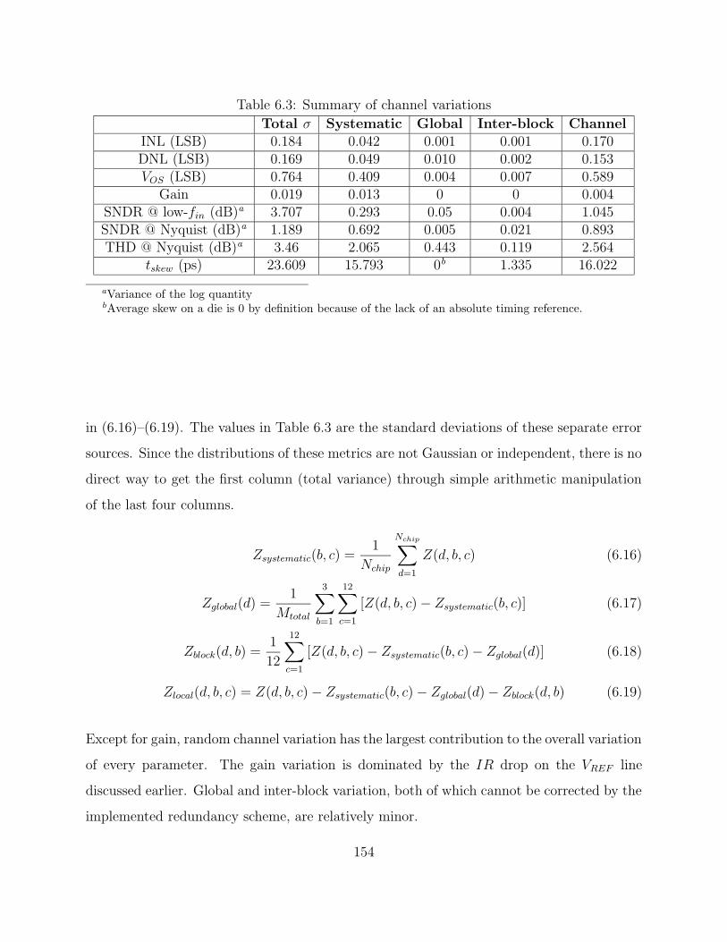
Table 6.3: Summary of channel variations
Total σ Systematic Global Inter-block ChannelINL (LSB) 0.184 0.042 0.001 0.001 0.170DNL (LSB) 0.169 0.049 0.010 0.002 0.153VOS (LSB) 0.764 0.409 0.004 0.007 0.589
Gain 0.019 0.013 0 0 0.004SNDR @ low-fin (dB)a 3.707 0.293 0.05 0.004 1.045SNDR @ Nyquist (dB)a 1.189 0.692 0.005 0.021 0.893THD @ Nyquist (dB)a 3.46 2.065 0.443 0.119 2.564
tskew (ps) 23.609 15.793 0b 1.335 16.022
aVariance of the log quantitybAverage skew on a die is 0 by definition because of the lack of an absolute timing reference.
in (6.16)–(6.19). The values in Table 6.3 are the standard deviations of these separate error
sources. Since the distributions of these metrics are not Gaussian or independent, there is no
direct way to get the first column (total variance) through simple arithmetic manipulation
of the last four columns.
Zsystematic(b, c) =1
Nchip
Nchip∑
d=1
Z(d, b, c) (6.16)
Zglobal(d) =1
Mtotal
3∑
b=1
12∑
c=1
[Z(d, b, c) − Zsystematic(b, c)] (6.17)
Zblock(d, b) =1
12
12∑
c=1
[Z(d, b, c) − Zsystematic(b, c) − Zglobal(d)] (6.18)
Zlocal(d, b, c) = Z(d, b, c) − Zsystematic(b, c) − Zglobal(d) − Zblock(d, b) (6.19)
Except for gain, random channel variation has the largest contribution to the overall variation
of every parameter. The gain variation is dominated by the IR drop on the VREF line
discussed earlier. Global and inter-block variation, both of which cannot be corrected by the
implemented redundancy scheme, are relatively minor.
154
6.6.3 Redundant Channel Selection and Yield
Once all of the channels on a die have been characterized, the “best” 36 are selected. What
constitutes the best channels is a matter of interpretation and depends on the target spec-
ifications. This section discusses selection strategies and proposes a cost function for auto-
mated channel selection. Overall yield improvement is presented as the number of redundant
channels per block is increased from 0 to 2.
First, channel selection is examined through an example, using the measured variation
plotted in Fig. 6-29, which shows relatively constrained distributions with a few outliers.
Channel 24 has the largest INL, channels 2 and 9 have the peak offsets, and channels 30 and
32 exhibit the worst timing skews. If global redundancy had been implemented, these five
channels could be replaced, improving the worst-case INL (0.50→ 0.31 LSB), peak-to-peak
offset (2.8→ 2.0 LSB), and rms timing skew (28.5→ 18.8 ps) by more than 30% at the same
time, with one channel left over. With the implemented block redundancy, however, channels
9, 24, and 30 are all located in the third block and cannot be replaced simultaneously.
Keeping channel 9 gives the same improvement in INL and skew but the peak-to-peak offset
is improved to only 2.5 LSB.
Before defining a strategy for automated channel selection, the effect of each of the
metrics must be considered. INL gives an indication of the worst case error for a slowly
varying input signal, whereas THD is the best characterization of the linearity error of a
high frequency input. As offset is corrected digitally, the analog offset, VOS, only limits the
peak signal before clipping occurs. The largest absolute offset voltage of the active channels
limits the peak input signal; the offsets of the other active channels have no effect. Gain
shows little random variation and is not used as one of the inputs for channel selection. The
overall SNDR has contributions from every channels’ SNDR plus the degradation of any of
the mismatch effects. While the low frequency SNDR does exhibit variation, it is highly
correlated with the offset due to the measurement setup where channels with the largest
offsets will clip the -1 dBFS input signal; it is therefore ignored for this selection procedure.
At high input frequencies, SNDR is often correlated with THD (cf. channel 4 in Fig. 6-
155

31); severe high frequency SNDR degradation that is uncorrelated with THD is usually a
sign of output mux failure and can lead to significant degradation of overall performance.
Finally, timing skew can lead to voltage errors for high frequency input and a corresponding
degradation in overall SNDR according to (6.8).
The selection process proposed here first eliminates the channels that are outliers of global
criteria. Then, if too many channels remain, the worst channels on the chip, relative only to
each other, are removed. For the global specification selection, every channel i is assigned a
total penalty Pi that is the sum of penalties from the individual parameters of that channel
(6.20). Each individual penalty is nonnegative, and the parameters kj weight the penalties
to normalize the different scales and impact of the penalties.
Pi =∑
j
kjpj,i j ∈ INL, VOS, SNDRH, THD, tskew (6.20)
The individual penalties are calculated as in (6.21)–(6.25), where (x)∗ is x for x > 0, and 0
otherwise.
pINL,i = (INLi − TINL)∗ (6.21)
pVOS,i =
(|VOS,i| − TVOS)∗ |VOS,i| = max
k|VOS,k|
0 o.w.(6.22)
pSNDRH,i = (TSNDRH− SNDRH,i)
∗ (6.23)
pTHD,i = (TTHD − |THDi|)∗ (6.24)
ptskew,i = (|tskew,i| − Ttskew)∗ (6.25)
For the global channel selection, the targets TINL, TVOS, TSNDRH
, TTHD, and Ttskeware fixed
for all chips. The offset penalty (6.22) is nonzero only for the channel with the largest
absolute offset of the non-eliminated channels. Initially, the penalties of all 42 channels
are calculated, and then the channel with the largest penalty is eliminated. The penalties
are then recalculated for the remaining 41 channels (only pVOS ,i might change), and the
156

Table 6.4: Weighting coefficients and target parameters for channel selection
Weighting Coefficient TargetkINL 1 TINL 0.4 LSBkVOS
0.5 TVOS1 LSB
kSNDRH3 TSNDRH
28 dBkTHD 1 TTHD 36 dBktskew
(1/30) ps−1 Ttskew30 ps
16 18 20 22 24 26 28 300
5
10
15
20
25
SNDRH
(dB)
Cou
nt
012
(a)
16 18 20 22 24 26 28 300
5
10
15
20
SNDRH
(dB)
Cou
nt
012
(b)
Figure 6-34: Histogram showing yield improvement as a function of the number of redundantchannels per block for the ADC operating at (a) 250 MS/s and (b) 125 MS/s.
remaining channel with largest penalty is eliminated. No more than two channels per block
can be eliminated. This process terminates when each block has two channels eliminated,
or no channels with nonzero penalties remain for blocks that have fewer than two channels
eliminated. If the latter case holds, the process is repeated but with the global targets Tj
replaced with the average of those parameters across the remaining channels. Although this
has not happened on any of the tested chips, it is conceivable that a block will still not have
eliminated 2 channels after this second step. This corresponds to the case where the channels
in this block are all very good, exceeding the averages of the other blocks. In this case, the
targets can be re-evaluated to the averages of this block, or channels can be eliminated at
random. The remaining 12 channels per block are chosen for operation.
157

0 10 20 30 4010
12
14
16
18
20
22
24
# tim
es c
hose
n
Channel #
Figure 6-35: Number of times the given channel was chosen as “good” out of the 24 dies.
This selection process is implemented using the weighting and target parameters in Ta-
ble 6.4. The high frequency SNDR is given the greatest weight as measurements have
demonstrated that it has the greatest impact on overall SNDR, and it is a good indicator
for a range of failures (e.g., noise, digital failures) that are not well captured by the other
metrics. Figure 6-34 shows the worst case SNDRH of active channels as a function of the
number of redundant channels per block. The number of redundant channels is varied by
the selection mechanism by forcing the last two or one channels to be eliminated first to
mimic the effect of zero or only one redundant channel per block. The number of chips with
a worst case SNDR of less than 28 dB decreases from 5 to 2 (Fig. 6-34(a)). Also shown is the
improvement at a slower sampling frequency of 125 MHz (Fig. 6-34(b)), which is measured
at 125 MS/s, where practically all timing related non-idealities are eliminated.
The results of the selection process can be compared with the systematic variation data
presented earlier by plotting the number of times a channel was selected (or, equivalently,
eliminated) over the 24 tested dies, as shown in Fig. 6-35. The worst channels are those
selected the fewest number of times. Channels 40 and 42 have the worst systematic timing
skews (Fig. 6-31), and channel 2 tends to have a higher INL and offset. The systematic
variation serves as a predisposition for a bad channel, but since none of the channels were
eliminated for every chip, random local variation can trump systematic variation for channel
158

Table 6.5: Yielding chips (out of 24) as a function of the number of redundant channels
Metric SpecificationRedundant Channels/block0 1 2
INL ≤0.6 LSB 14 21 21VOS ≤2 LSB 19 23 24
SNDRH ≥27 dB 19 22 22THD ≥33 dB 21 23 24
tskew (rms) ≤15 ps 24 24 24SNDRH
a ≥27 dB 17 23 23All specs 10 21 21
aSNDR of interleaved ADC
selection.
A summary of the improvement in these parameters with redundancy is shown in Ta-
ble 6.5. For best results, the target for channel selection (Table 6.4) should be at least as
conservative as the specifications listed in this table. Also included in the table is the yield of
the overall SNDR for the interleaved chip, which also shows improvement with redundancy.
6.6.4 BIST Extension
The channel selection procedure described in this chapter is offline and suitable for initial
die testing but is not directly useful for dynamic channel selection after system deployment.
For some applications, it is desirable to change the active channels in response to changing
environmental conditions, such as voltage, temperature, or in response to process aging. To
highlight the usefulness of BIST, Figure 6-36 presents the correlation of selected channels
on a chip for six different temperature settings from 0 to 80 C. While channels 36 and 42,
with the highest timing skews, are least used, the dominant failure mechanisms change at
high temperatures from skew to linearity, meaning that no channel is the worst across the
entire temperature range. This section briefly describes BIST procedures that could lead to
automatic, dynamic channel selection. A BIST operates at a very low duty cycle, and its
energy overhead during normal operation would be confined to leakage power only.
The actual channel selection procedure (6.20)–(6.25) is implementable using a finite state
159

0 10 20 30 400
1
2
3
4
5
6
# tim
es c
hose
n
Channel #
Figure 6-36: Number of times the given channel was selected for active operation, wheremeasurements were performed on a single die at 6 different temperature settings from 0 to80 C. While some channels performed well across all temperatures, no channel was the worstat every setting.
machine (FSM) and simple adder/comparator. The difficult part is measuring the perfor-
mance metrics directly on-chip. One advantage of having redundant channels is that fore-
ground characterization/calibration of the channels can be done while still leaving 36 active
channels. This is similar to the approach proposed in [47] where an extra channel is included
specifically to allow foreground calibration of channels without disturbing overall ADC per-
formance. There may be some performance degradation because the “best” 36 channels
cannot be selected while channel calibration is being performed, but 36 channels are always
available.
The static linearity and offset can be directly measured using the SAR calibration pro-
cedure in [31], where the calibration engine and resistive sub-DAC can be shared among all
channels. Gain errors can be measured using the technique in [47].
Dynamic errors are more difficult to measure. A signal generator can be included on-chip
for foreground calibration/characterization. Another possibility is to measure the channels
with the actual input signal. Jamal, et al., proposed adding chopping switches at the input
of each channel, thereby creating a mechanism to calibrate offset, gain, and timing skew
errors with arbitrary input signals [53].
160

Table 6.6: Performance summary of 36+6-way interleaved ADC
Technology 65-nm CMOS 1P6MResolution 5 bit
Input Range 700 mVpp DifferentialSampling Rate 250 MS/s 400 MS/s
Core Supply Voltage 800 mV 1.0 VSampling Supply Voltage 1.2 V 1.2 V
SNDR (DC) 29.2 dB 28.8 dBInput frequency 117 MHz 188 MHz
SNDR 28.4 dB 27.8 dBSFDR 47.5 dB 43.7 dBTHD -44.6 dB -45.7 dB
Analog Power 270µW 650µWDigital Power 930µW 2.01 mWTotal Power 1.20 mW 2.66 mW
Figure of Merit (1.1) 240 fJ/conv. step 350 fJ/conv. stepActive Area 2.10 mm × 1.45 mm
Another method to measure dynamic errors is to directly compare the outputs of multiple
channels sampling at the same time. With two redundant channels per block, up to three
channels can sample the same input (assuming an appropriate modification of the channel
synchronization circuitry, Fig. 6-7), and directly comparing the outputs gives the relative
errors of the channels. This method can be combined with chopping to give meaningful
dynamic results even for stationary inputs. Sampling multiple channels at the same time does
introduce extra potential for coupling errors, which must be considered when determining
the effectiveness of this scheme.
6.7 Chip Summary
This chapter has presented the design of a robust highly-parallel ADC designed to operate
near the minimum mixed-signal energy point. The ADC is composed of three blocks with
fourteen channels each, two of which are redundant. Clock distribution power is kept in check
by distributing a single low frequency/voltage clock to the channels within a block; only one
161

sampling switch per block receives the precise full speed sampling clock. This master switch
defines the sampling instant per block, reducing timing skew, a pernicious problem to correct
digitally. Finally, redundant channels counteract yield loss due to local variations in parallel
circuits. The redundancy implementation requires minimal overhead and allows for a highly
energy efficient final design. The ADC performance is summarized in Table 6.6.
162
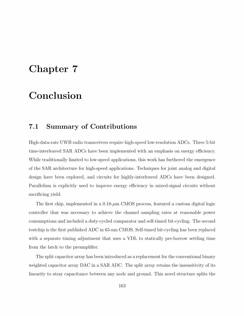
Chapter 7
Conclusion
7.1 Summary of Contributions
High-data-rate UWB radio transceivers require high-speed low-resolution ADCs. Three 5-bit
time-interleaved SAR ADCs have been implemented with an emphasis on energy efficiency.
While traditionally limited to low-speed applications, this work has furthered the emergence
of the SAR architecture for high-speed applications. Techniques for joint analog and digital
design have been explored, and circuits for highly-interleaved ADCs have been designed.
Parallelism is explicitly used to improve energy efficiency in mixed-signal circuits without
sacrificing yield.
The first chip, implemented in a 0.18-µm CMOS process, featured a custom digital logic
controller that was necessary to achieve the channel sampling rates at reasonable power
consumptions and included a duty-cycled comparator and self-timed bit-cycling. The second
testchip is the first published ADC in 65-nm CMOS. Self-timed bit-cycling has been replaced
with a separate timing adjustment that uses a VDL to statically pre-borrow settling time
from the latch to the preamplifier.
The split capacitor array has been introduced as a replacement for the conventional binary
weighted capacitor array DAC in a SAR ADC. The split array retains the insensitivity of its
linearity to stray capacitance between any node and ground. This novel structure splits the
163

MSB capacitor into an identical copy of the rest of the array; it does not require an increase
in the total capacitance or area of the array. Then, during every bit decision after the first,
only one capacitor from the MSB or main subarray is switched, reducing the total switching
energy by 37%. In addition, the total current drawn for a conversion is made symmetric
with the input signal, removing any even order harmonics from the input-signal dependent
current drawn from a reference voltage buffer. Finally, correlations in unit capacitors for
neighboring bit decisions reduce the DNL by√
2 with the same INL.
To address the total power consumption of an ADC, a mixed-signal energy model has been
developed that can find the genuine optimum energy point, considering both the analog and
digital circuits and their interactions. The model’s framework has been designed to allow
flexibility in analyzing tradeoffs across the analog/digital boundary; a coupled behavioral
model shows the response of the ADC to non-idealities, variations, and digital correction
schemes. The optimization was performed to find the best combination of operating voltages
and number of parallel channels, which is limited by clock and input buffer
While the optimum number of channels is 60, the minimum is sufficiently broad that 36
channels suffers less than a 10% energy penalty and was chosen as the level of parallelism in
the final testchip. This chip is the first demonstration of the use of parallelism in mixed-signal
circuits specifically to drive down the voltage for energy savings. Offset mismatch between
channels is corrected digitally. Timing skew is minimized using a hierarchical top-plate
sampling network that has been extended to permit overlapped sampling periods with a slow
turn-on input switch drive for reduced crosstalk between channels. The channels have been
partitioned into three blocks, and the clock distribution has a precise domain connected only
to the master sampling networks and an imprecise domain, at lower voltages, distributed to
the channels. Finally, this work is the first implementation of channel redundancy to combat
yield loss in parallel ADCs.
A comparison of the three ADCs presented within this thesis with state-of-the-art high-
speed low-resolution converters is shown in Fig. 7-1 and Table 7.1, using the figure of merit
defined in (1.1) for comparison. The final two testchips show performance similar to the
164

200 400 600 800 1000 12000.1
0.2
0.3
0.4
0.5
0.6
0.7
0.8
0.9
G2
G2
G3
G3
A
B
C
D
E
F
Sampling Frequency (MHz)
FO
M (
pJ/c
onv.
ste
p)
SARFlashPipelinedSubrangingThis work
Figure 7-1: Comparison of energy efficiency figure of merit for state-of-the-art converterswith a resolution ≤8 bits and sampling rates exceeding 100 MHz.
best published converters to date. In addition, the SAR ADC is clearly shown as being
competitive with the more traditional high-speed architectures.
7.2 Conclusions
A unifying theme throughout this thesis has been the use of parallelism specifically to improve
the energy efficiency of mixed-signal circuits, in contrast to its conventional role of only
increasing maximum operating speeds. Time-interleaving allows the energy efficient slow
SAR architecture to operate at speeds comparable to non-interleaved flash converters but at
reduced power. Furthermore, increased levels of parallelism slow individual channel operation
and permit lower voltage supplies and additional improvement in energy efficiency. While
the beneficial relationship between parallelism and energy is not new [94], it has been mainly
confined to digital circuits.
Perhaps it is not surprising, because of the significant digital power consumption in
the three chips, but many of the ideas in this thesis are similar to or inspired by digital
circuit techniques. Clearly, the dynamic logic controller is a direct implementation of high-
165
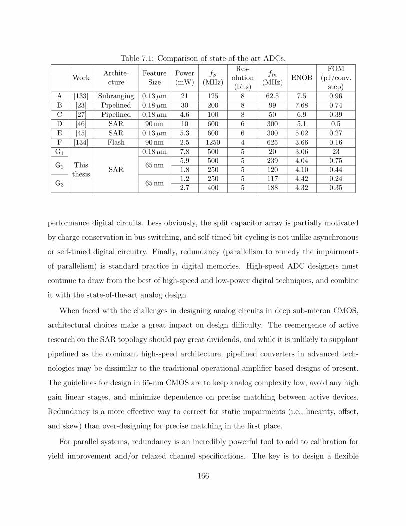
Table 7.1: Comparison of state-of-the-art ADCs.
WorkArchite-
ctureFeature
SizePower(mW)
fS
(MHz)
Res-olution(bits)
fin
(MHz)ENOB
FOM(pJ/conv.
step)
A [133] Subranging 0.13 µm 21 125 8 62.5 7.5 0.96
B [23] Pipelined 0.18 µm 30 200 8 99 7.68 0.74
C [27] Pipelined 0.18 µm 4.6 100 8 50 6.9 0.39
D [46] SAR 90 nm 10 600 6 300 5.1 0.5
E [45] SAR 0.13 µm 5.3 600 6 300 5.02 0.27
F [134] Flash 90 nm 2.5 1250 4 625 3.66 0.16
G1
Thisthesis
SAR
0.18 µm 7.8 500 5 20 3.06 23
G2 65 nm5.9 500 5 239 4.04 0.751.8 250 5 120 4.10 0.44
G3 65 nm1.2 250 5 117 4.42 0.242.7 400 5 188 4.32 0.35
performance digital circuits. Less obviously, the split capacitor array is partially motivated
by charge conservation in bus switching, and self-timed bit-cycling is not unlike asynchronous
or self-timed digital circuitry. Finally, redundancy (parallelism to remedy the impairments
of parallelism) is standard practice in digital memories. High-speed ADC designers must
continue to draw from the best of high-speed and low-power digital techniques, and combine
it with the state-of-the-art analog design.
When faced with the challenges in designing analog circuits in deep sub-micron CMOS,
architectural choices make a great impact on design difficulty. The reemergence of active
research on the SAR topology should pay great dividends, and while it is unlikely to supplant
pipelined as the dominant high-speed architecture, pipelined converters in advanced tech-
nologies may be dissimilar to the traditional operational amplifier based designs of present.
The guidelines for design in 65-nm CMOS are to keep analog complexity low, avoid any high
gain linear stages, and minimize dependence on precise matching between active devices.
Redundancy is a more effective way to correct for static impairments (i.e., linearity, offset,
and skew) than over-designing for precise matching in the first place.
For parallel systems, redundancy is an incredibly powerful tool to add to calibration for
yield improvement and/or relaxed channel specifications. The key is to design a flexible
166

enough architecture that the overhead for enabling and disabling parts is small (in the final
testchip, it was only a few gates per channel). By using redundancy at a higher level of the
hierarchy, more faults can be corrected, particularly if fault models are not known a priori.
Unfortunately, redundancy is not a panacea: it cannot correct for errors above the level
where redundancy is applied (e.g., the output mux failure at the block level), but significant
yield improvement is achievable by applying redundancy and calibration at multiple levels
of the hierarchy, and reserving the most conservative design for the non-correctable portions
of the circuit.
7.3 Future Directions
While the mixed-signal energy optimization was set up for a SAR ADC, the design method-
ology is directly applicable to other ADC topologies, many of which have significant digital
power (cf. Fig. 5-1) and opportunities for moving analog complexity to the digital domain.
In addition, many larger systems, from radios to sensor interfaces, span the analog/digital
boundary and can also be optimized using such a model. A single tool that can integrate
the behavioral model and energy model could make this optimization methodology more
practical. In addition, different levels of abstraction should be added to this model, from
transistor level to digital synthesis. Ultimately, such a tool could lead to automated design
of mixed-signal circuits.
Redundancy is still an underused technique, particularly in the analog and mixed-signal
domains. This work showed the advantage of redundancy over sizing for yield improvement in
parallel circuits, but additional research is necessary to explore the comparative advantages
of redundancy and calibration. If the overhead of redundancy is sufficiently small, it may
have an energy advantage over calibration or other correction methods because, once the
“bad” blocks have been eliminated, the remaining “good” blocks operate without the added
correction complexity and power. For circuits that are not inherently parallel, redundancy
may still be applicable. For instance, as shown in the split ADC (not to be confused with
the split capacitor array), a high accuracy block can be split into two lower accuracy blocks
167

without an overall increase in power or decrease in resolution [135]. This introduction of
parallelism was used to speed up background calibration, but redundancy could be applied
to the lower accuracy sub-blocks, improving the overall yield. Redundancy is certainly not a
panacea, as it cannot get around certain circuit limitations, such as noise, but its potential
has certainly not been fully explored.
For all of these yield improvement techniques, there needs to be a better understanding of
variation and fault models. While significant data exists on transistor or capacitor variation
and mismatch, easily incorporating this information into large mixed-signal circuits remains
a challenge. Monte Carlo simulations are simply not practical for a large system, particularly
when local variation requires statistical models of thousands of elements varying indepen-
dently. For this thesis, Monte Carlo simulations were done only for very small circuit blocks
(e.g., comparator, sampling switch, etc.), and the variations of these blocks were considered
independent. Unfortunately, not every block, such as the clock distribution, or SAR digital
controller were able to be fully simulated for local variation, and therefore no comprehen-
sive fault model could be generated a priori. A simulation or design methodology that can
translate the available process variation data into overall fault models of complex circuits
would be an invaluable asset, particularly for advanced and still emerging technologies.
168

Appendix A
SAR Behavioral Model
As an aide during the design process, a behavioral model of the SAR ADC is presented in
this chapter. During the early design period, the behavioral model is used to determine
the response to the ADC to various design tradeoffs. Even after design has begun, the be-
havioral model is used for variation analysis. For global variation, corner models are often
available. These offer a limited number of discrete simulations that must be performed to
cover the outer reaches of the process space. Corner models, however, can be too conserva-
tive in some cases and do not give predictions about the distribution of the resultant chips.
In addition, corner models do not apply to local variation. Thus, Monte Carlo simulations
are used to handle statistical variations, but they require hundreds to thousands of runs. A
transistor-level simulation of a single conversion of a channel takes on the order of minutes,
making Monte Carlo simulations extremely time consuming at best. For longer simulations,
such as timing skew between neighboring channels on a long sinusoid, transistor-level Monte
Carlo simulations are completely impractical at present. Behavioral simulations offer an
alternative to transistor-level simulations, where accuracy of the final results is traded for
speed. Several behavioral simulation tools are available [136, 137] that can provide various
schematic capture, netlisting, and simulation capabilities. In this work, a behavioral model
was implemented directly in Matlab. This appendix describes the general setup of the be-
havioral model and its capabilities. The results of the behavioral model are used throughout
169

Si
Sampling
Block
VX
Digital
Logic
DT SAR
Array
Capacitor
Signal
AnalysisINL/DNLSNDR
THD/SFDRDout
Vin[n]
SE/Diff.Conv./Split
Figure A-1: Block diagram of the behavioral model. The analysis and digital control blockare ideal, while the remaining blocks can model non-idealities.
the thesis.
Figure A-1 shows the structure of the behavioral model. At its core is a discrete time
SAR ADC that takes sampled analog values as input and produces the corresponding digital
outputs. This discrete time SAR includes as sub-blocks a capacitive DAC, a comparator,
and digital control logic. The discrete time inputs are generated by the sampling block,
which can create arbitrary ramp and sinusoidal inputs. The outputs are processed by an
analysis block that computes SNR, SNDR, THD, SFDR, offset, and INL/DNL. All of the
blocks behave ideally by default. With the exception of the digital logic and signal analysis
block, they also model various non-idealities, as described below. Unless specified below, the
positive and negative references are 1 and 0, respectively.
A.1 Block Descriptions
The DAC can be switched between the binary weighted or split capacitor arrays and be
single-ended or differential. Each capacitor within the array includes the sum of i.i.d. errors
from its unit capacitors plus a systematic error that models the layout induced errors from
nonlinear coupling between top and bottom plate routing. For instance, the MSB capacitor
in the conventional array has total capacitance
CMSB =2b−1
∑
i=1
(
C0 + N(0, σC0))
+ ∆CMSB. (A.1)
170

0 0.05 0.1 0.15 0.20
0.2
0.4
0.6
0.8
INL
(LS
B)
σdet
/C0
Binary arraySplit arraySplit array flipped
Figure A-2: Behavioral simulation showing the effect of systematic errors of differentialcapacitor arrays on INL. The model uses ∆Ck ∼ N(0, kσdet). The bottom curve flips thesubarrays of the differential split capacitor arrays.
The output of the array is defined by (4.3)–(4.5) where CT and CB are appropriately modified
to include the effect of capacitor variation.
The systematic error can be used to predict the INL and DNL if ∆Ci are extracted
from the layout. In addition, it can be used to compare the sensitivity of the different
arrays’ linearities to layout induced errors. Without extracted parasitics, a simplistic error
model can be used where, for a capacitor consisting of k unit capacitors, the systematic
error from routing is ∆Ck ∼ N(0, kσdet). This error model is not expected to correspond to
most layout induced errors, but without knowledge of the actual layout, this is a reasonable
model for early in the design cycle. While it may seem that this definition means that σC0
in (A.1) can be replaced with√
σ2C0
+ σ2det, that only holds for a single-ended array of a
non-time-interleaved converter. Assuming that an identical layout is used for both halves
of a differential array and for every channel in an interleaved ADC, then systematic errors
are correlated between arrays and channels, whereas the random variation from σC0will be
independent.
Figure A-2 compares the impact of systematic errors on the linearity of differential ADCs
with different capacitor array configurations. The upper two curves are for the binary
weighted and split capacitor arrays where both of the arrays in the converter have iden-
171

tical errors. The lower curve is for an ADC where the two split capacitor arrays have flipped
subarrays. For an identical layout of the bottom plate routing within the array, the digital
signals to the switches are interchanged between C5,k and Ck between the two arrays. This
is possible because the two subarrays are symmetric. For this type of systematic error, the
overall linearity is improved by flipping the subarrays for the two differential split capacitor
arrays.
The ideal comparator outputs a 1 if the input VX > 0 and 0 otherwise. Non-idealities
that can be modeled include the offset VOS ∼ N(0, σOS) and finite settling time constant τ .
The comparator output is
COMP [i] =
1 VX [i] + (VX [i − 1] − Vx[i])e−1/τ > VOS
0 otherwise,(A.2)
where i represents the current bit decision period, and VX [0] = 0 because the comparator is
autozeroed during the sampling period at the start of every conversion.
The digital logic generates the appropriate switch signals for the capacitor array using
the conventional 1-step switching method [66] or the split capacitor array switch method
from Fig. 4-8. No non-idealities are modeled.
The sampling block can pass along arbitrary input signals, or it can generate ramps and
sine waves for static and dynamic testing, respectively. While sine waves can be used to
determine INL and DNL [85], it is a statistical method and requires many more samples
that are unnecessary when an ideal ramp can be generated. The generated sine wave has
the form
Vin[n] = 0.5 + VOS +A
2sin(
2πfin(n/fS + ∆tskew[n] + δtjitter[n]))
. (A.3)
The jitter is assumed to be Gaussian and independent from sample to sample, so that
δtjitter[n] ∼ N(0, σjitter). The timing skew between channels in an interleaved ADC is mod-
eled by ∆tskew, which is periodic with M , the number of channels.
172

−1
0
1IN
L
0 10 20 30−1
0
1
2
DN
L
Dout
Figure A-3: Static linearity of the ADCwith insufficient comparator settling time oftsettle = 2τ .
0 0.5 13.8
4
4.2
4.4
4.6
4.8
5
EN
OB
INL (LSB)
Figure A-4: Scatter plot showing correlationbetween ENOB and INL under the presenceof capacitor mismatch (σC0
/C0 = 0.1).
A.2 Behavioral Model Results
Several of the results from the behavioral model are included elsewhere (cf. Figs. 2-4, 4-11, 5-
6, and 6-2). Presented here is a quick summary of some of the other result highlights. These
are included to demonstrate some of the capabilities of the behavioral model. Figure A-3
shows the static linearity when the comparator is too slow. In this case, the comparator is
only settling for 2τ , which leads to severely degraded linearity, particularly at the MSB/2
transitions, when the worst case settling behavior of the comparator is exercised.
Figure A-4 is a scatter plot of the ENOB and INL for the case of only random capacitor
errors. In this still relatively ideal case, the INL effectively sets a lower bound on the ENOB;
however, when noise and other non-idealities are included, the ENOB will be lower.
Finally, non-ideal sampling is presented in Fig. A-5, which plots the SNDR dependence
on the the skew and jitter standard deviations as well as its dependence on input frequency
for fixed variation. These results were used to determine the design specifications of the
testchips presented in this thesis.
173
0 2 4 6
x 10−3
26
27
28
29
30
31
32
SN
DR
(dB
)
σ/TS
σ
jitter
σskew
(a)
0 0.1 0.2 0.3 0.4 0.522
24
26
28
30
32
SN
DR
(dB
)
fin
/fS
σjitter
/TS = 0.01
σskew
/TS = 0.02
(b)
Figure A-5: Behavioral model results showing the degradation in SNDR due to non-idealsampling. On the left, the degradation due to sampling and skew are compared for a twiceNyquist input. On the right, frequency dependence of the sampling error is plotted.
174

Appendix B
Closed-Form Expression for SAR INL
This section presents the closed-form expression for the INL of a SAR ADC under the case
of i.i.d. Gaussian errors in the unit capacitors in the array. In Chapter 4, the variance of the
error voltage grows linearly with the output code y (4.22), but as shown in Fig. 4-11, the
INL is maximized for y = 2b−1 and then decreases for larger y. This analysis begins with
(4.20), repeated here for clarity.
VX(y)
VREF
=
b∑
n=1
(
2n−1C0 + δn
)
Sn
2bC0 + ∆C=
b∑
n=1
(
2n−1C0 + δn
)
Sn
2bC0 +b∑
n=1
δn
. (B.1)
Here ∆C will not be ignored for now. In addition, rather than grouping the errors into the
constituent capacitors, the δn will be expanded into the explicit errors of the unit capacitors,
δn =∑n
j=1 εj, where the ordering of εj is ignored, as the specific ordering is only needed for
the DNL calculation (cf. (4.25)). Splitting δn and substituting y =∑b
n=1 Sn2n−1, (B.1) can
be written as
VX(y)
VREF
=
yC0 +
y∑
j=1
εj
2bC0 +2b∑
l=1
εl
. (B.2)
175

The error is the deviation of this voltage from the ideal steps that are placed along a line
from 0 to 1, giving
Verr(y)
VREF
=
yC0 +
y∑
j=1
εj
2bC0 +2b∑
l=1
εl
− y
2b
=
y2bC0 +
y∑
j=1
(2bεj) − y2bC0 −2b∑
k=1
yεk
2b(2bC0 +2b∑
l=1
εl)
.
(B.3)
At this point, it is safe to make the approximation that∑2b
l=1 ¿ 2bC0, which simplifies (B.3)
to
Verr(y)
VREF
=
y∑
j=1
(2b − y)εj −2b∑
k=y+1
yεk
22bC0
. (B.4)
This error is the sum of independent zero-mean Gaussian random variables and thus is also
Gaussian with a zero mean. The variance can be calculated by noting that all of the errors
in the unit capacitors are independent with E[ε2j ] = σ2
0.
E[V 2err(y)]
V 2REF
=(2b − y)2y + y2(2b − y)
24bC20
σ20 =
y(2b − y)
23b· σ2
0
C20
(B.5)
The standard deviation of the INL, in terms of LSBs is
σINL(y) =
(
E[V 2err(y)]
V 2REF
)1/2
· 2b = 2−b/2√
y(2b − y)σ0
C0
LSB. (B.6)
Figure B-1 shows that the behavioral model results from Fig. 4-11 match (B.6) for b = 5
and σ0/C0=3%.
176
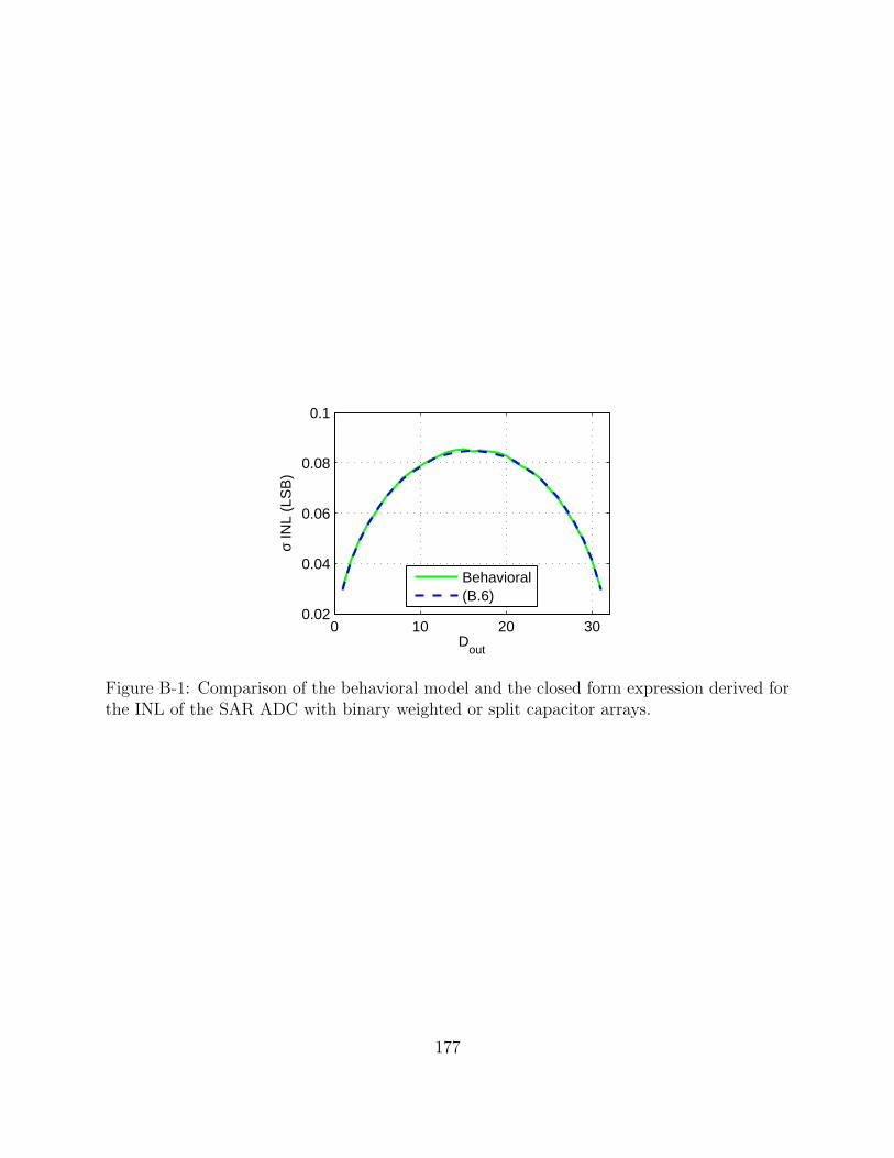
0 10 20 300.02
0.04
0.06
0.08
0.1
σ IN
L (L
SB
)
Dout
Behavioral(B.6)
Figure B-1: Comparison of the behavioral model and the closed form expression derived forthe INL of the SAR ADC with binary weighted or split capacitor arrays.
177

178

Appendix C
Energy Model Block Equations
Chapter 5 described the framework of the mixed-signal energy optimization, and it included
highlights of the block energy models. Below are the details of these models, including the
equations that determine the energy and output variables of the block. This appendix is very
detailed and not for the faint of heart. For each block description, there is listed a table with
the parameters required for that block (not including the global optimization parameters
of Table 5.1). The parameter type is one of: A = global architectural parameters; P =
process specific parameter; I = block input parameter; or, O = block output parameter.
Any parameters listed in the equations that are not in the tables are local parameters (L in
Fig. 5-3). After all the blocks are detailed, there is a summary of the required process data
and set of simulations used to generate that data.
C.1 Digital Logic
The core logic is simply the switching and leakage contributions from the SAR controller.
Edig,core =b
b0
(
Cdig0V2DDD + Ileak0VDDDtconv
)
(C.1)
Here, Cdig0 is an effective switched capacitance for the entire digital block and was taken
from measurements of the first 65-nm testchip, with b0 = 5. For ease of technology scaling,
179

41 16 MSW
L
4L
Figure C-1: Buffering chain used to drive the large capacitor array switches from the outputof the control logic block. The total number of inverters inserted is L.
the digital energy can be referenced to a simple logic gate (e.g., an inverter with fan-out of
4 (FO-4)) times some architecture-dependent but process-independent multiplicative factor.
Ileak0 is the measured leakage current from the previous chip.
The second digital energy component is for driving the switches of the capacitor array,
which are separated into the sampling switch and then bit-cycling switches. Buffering is
automatically inserted to drive the large capacitive load of the switches as seen in Fig. C-1.
The buffer chain assumes a scaling factor of 4 between successive inverters. Therefore, from
the output of a minimum size inverter to the switch input, the number of stages that must
be inserted is
Lk = log4
Csw,k
CFO4,1
(C.2)
where k is samp or bc to represent the sampling or bit-cycling switch capacitive load. The
capacitive load that can be driven by a single minimum size inverter is CFO4,1. The number
of buffers must be an integer, and a floor or ceiling function could be applied to (C.2), but
the model is simpler if it is treated as a real number, and the error from not rounding is
negligible. Then the total switched capacitance in the buffer chain, normalized to that of
the minimum size inverter Csw,FO4, is
Cbuf,k
Csw,FO4
=1 − 4Lk+1
1 − 4. (C.3)
Finally, the energy of the buffer chains is the sum of the switching energy and, for the
sampling switch drive when VDDS 6= VDDD, the energy of inserted level shifters, which is
relatively small and could be neglected. Leakage power integrated over a conversion is also
180

included for all of these blocks, but it is omitted from the equations for the sake of brevity.
Ebuf,samp = Cbuf,sampV2DDS + Csw,levelshiftV
2DDS (C.4)
Ebuf,bc =3
4Cbuf,bcV
2DDS (C.5)
The buffer energies and delays are referenced to that of a single minimum size FO-4 inverter.
The coefficient 3/4 in (C.5) reflects the expected number of transitions for the bottom plate
switches in the split capacitor array. The total energy is
Edigital = Edig,core + Ebuf,samp + Ebuf,bc. (C.6)
The charge pump supplies the current for the sampling buffer chain, which is
Iload,cp =Ebuf,samp
tconvVDDS
. (C.7)
The setup and propagation delays through the digital logic are used to verify functionality
and determine the amount of time available for the capacitor array and preamplifier settling.
tsetup = ts,DFF + Nsetuptd,FO4 (C.8)
tpd,samp = tc→q(VDDD) + Nsamptd,FO4(VDDD) + td,levelshift + Lsamptd,FO4(VDDS) (C.9)
tpd,bc = tc→q + Nbctd,FO4 + Lbctd,FO4 (C.10)
The terms Nsetup, Nsamp, and Nbc represent the logic depths of the core digital logic that
correspond to the setup time and sampling and bit decision propagation delays, respectively.
These are architecture dependent and are 3, 4, and 1, respectively, for the logic controller
described in Section 6.4.2.
The many parameters used in the digital logic block energy model are listed in Table C.1
181
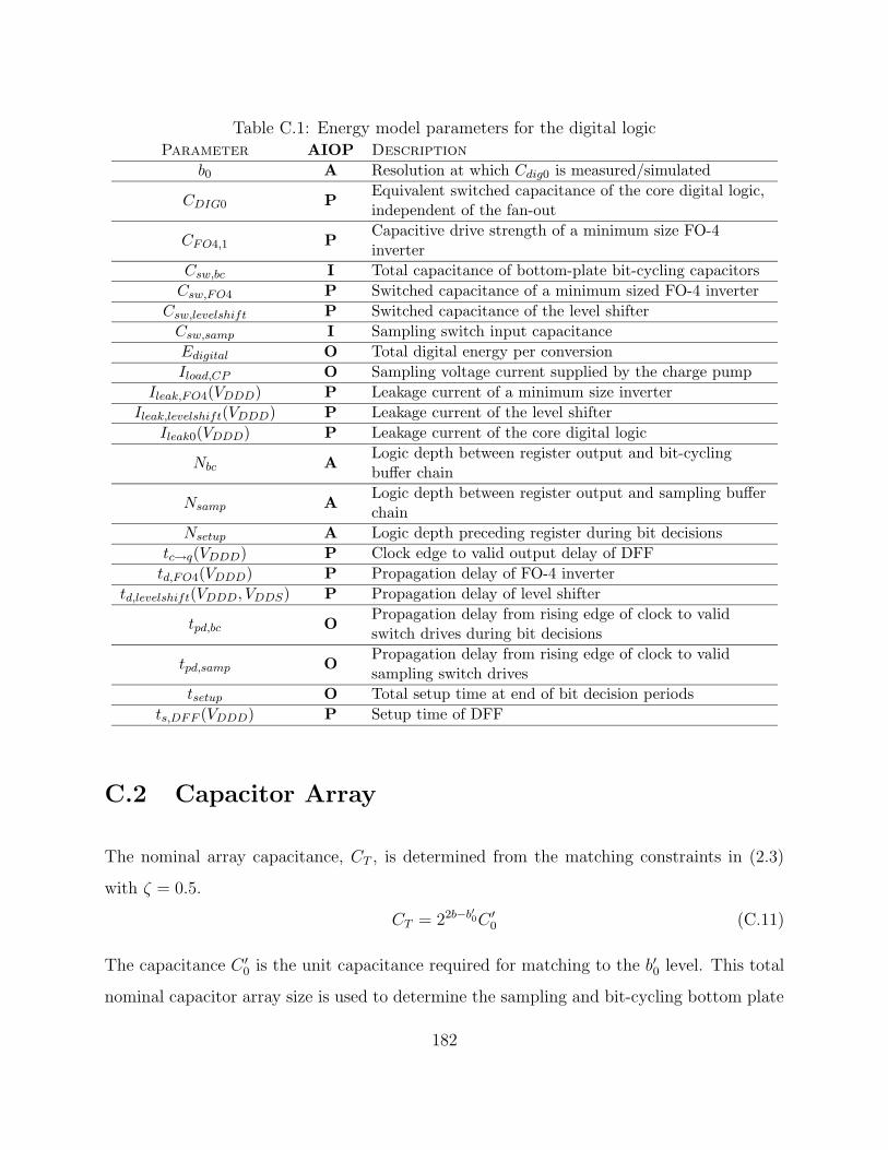
Table C.1: Energy model parameters for the digital logicParameter AIOP Description
b0 A Resolution at which Cdig0 is measured/simulated
CDIG0 PEquivalent switched capacitance of the core digital logic,independent of the fan-out
CFO4,1 PCapacitive drive strength of a minimum size FO-4inverter
Csw,bc I Total capacitance of bottom-plate bit-cycling capacitors
Csw,FO4 P Switched capacitance of a minimum sized FO-4 inverter
Csw,levelshift P Switched capacitance of the level shifter
Csw,samp I Sampling switch input capacitance
Edigital O Total digital energy per conversion
Iload,CP O Sampling voltage current supplied by the charge pump
Ileak,FO4(VDDD) P Leakage current of a minimum size inverter
Ileak,levelshift(VDDD) P Leakage current of the level shifter
Ileak0(VDDD) P Leakage current of the core digital logic
Nbc ALogic depth between register output and bit-cyclingbuffer chain
Nsamp ALogic depth between register output and sampling bufferchain
Nsetup A Logic depth preceding register during bit decisions
tc→q(VDDD) P Clock edge to valid output delay of DFF
td,FO4(VDDD) P Propagation delay of FO-4 inverter
td,levelshift(VDDD, VDDS) P Propagation delay of level shifter
tpd,bc OPropagation delay from rising edge of clock to validswitch drives during bit decisions
tpd,samp OPropagation delay from rising edge of clock to validsampling switch drives
tsetup O Total setup time at end of bit decision periods
ts,DFF (VDDD) P Setup time of DFF
C.2 Capacitor Array
The nominal array capacitance, CT , is determined from the matching constraints in (2.3)
with ζ = 0.5.
CT = 22b−b′0C ′0 (C.11)
The capacitance C ′0 is the unit capacitance required for matching to the b′0 level. This total
nominal capacitor array size is used to determine the sampling and bit-cycling bottom plate
182

0 0.2 0.4 0.6 0.8 10
0.2
0.4
0.6
0.8
1
Vin
g ds (
Nor
mal
ized
)
NFETTransmission Gate
Figure C-2: Normalized conductance, gds, of the NFET and transmission gate bottom plateswitch versus the input voltage.
switch sizes.
C.2.1 Sampling
The conductances of the NFET and TG sampling networks are plotted in Fig. C-2 versus
the input voltage. As shown in the figure, NFET sampling can only be used if the reference
voltage is confined to be low. The step response portion of sampling requires that
tsample > kslew(b + 1) ln(2)τsamp. (C.12)
The factor kslew is used to model the nonlinear slewing portion at the onset of sampling and
is determined from simulations to be 1.9. The time constant for sampling is approximately
τsamp = CS/gds,min, where gds,min is the minimum conductance of the switch (from Fig. C-2)
between 0 and VREF .
Accurately tracking a high frequency input signal is more complicated because the non-
linearity arises only from the variation of the conductance across the input range. A flat
conductance, independent of its value, will not produce any harmonic distortion. Volterra
analysis [138] could be used to formulate a closed form expression for the distortion, which
183

MB
WB/Lmin
VDDS
0
VDDS
0
MT
WT/Lmin
CS
Cpar,TCpar,B
X
Figure C-3: NFET sampling network with associated parasitic capacitances Cpar,B ∝ WB
and Cpar,T ∝ WT .
can then lead to proper sizing of the switches; however, this approach is highly dependent
upon the particular device characteristics and makes the model much more difficult to setup
and transition to new process nodes. Instead, this work uses a much simpler model that
produces a conservatively sized sampling switch. The most attenuation of an input signal
across SB occurs at the maximum frequency and at the voltage where the switch conduc-
tance is minimum. By restraining the attenuation at this point to less than half an LSB, the
attenuation across the entire input signal range will be no more than this, and the input will
be accurately tracked across the bottom plate switch. This condition is quantified in (C.13)
and has been verified by simulations to produce a conservatively sized sampling network.
The simulations predict that the network has a total harmonic distortion (THD) < −43 dBc
across the entire range of VDDS and VREF values, sufficient for a 5-bit ADC.
1√
1 + (fSτsamp/2)2> 1 − 2−(b+1) (C.13)
The stricter bound of (C.12) and (C.13) sets the maximum τsamp. The sizing of the NFET
sampling network to meet this bound is discussed here. The optimization of the transmission
gate network follows a similar process but is more complex because of an added free variable;
it is discussed in Appendix D. For a fixed VREF , VDDS , and τmax, the two remaining free
variables are the widths of the bottom and top plate switches, WB and WT , respectively.
The effect of the parasitic capacitance of the switches is added, as shown in Fig. C-3, where
Cpar,k ∝ Wk for k ∈ B, T. For the bandwidth constraint (C.13), the total time constant
184
of the sampling network is determined using open circuit time constants (OCTC) as
τsamp = CS
(
1
gds,T
+1
gds,B
)
+Cpar,T
gds,T
+Cpar,B
gds,B
. (C.14)
The bottom plate switch conductance is gds,B = minVS
gds(VG, VS) = gds(VDDS, VREF ) because
the minimum conductance always occurs at the largest input signal for the NFET switch.
The top plate switch conductance is simply gds,T = gds(VDDS, 0). The last two terms in (C.14)
are independent of the switch widths and are only dependent upon the relevant voltages in
the circuit. Thus, to determine WT and WB, an effective time constant
τeff = τsamp −Cpar0,T
gds0,T
− Cpar0,B
gds0,B
(C.15)
is used. The sampling network model fails if τeff < 0. It should be noted that OCTC is only
useful to find a conservative lower bound on the 3 dB bandwidth and is not directly related
to settling time of a non-first-order system; however, for most designs, including the optimal
one, CS À Cpar,T + Cpar,B and the sampling network is effectively first order, making the
error from using τeff in both the tracking and settling time constraints negligible.1 Using
(C.14), (C.15), and gds,k = (W/W0)gds0,k, WB can be expressed in terms of WT as
WB =1
(
τeff
CSW0− 1
WT gds0,T
)
gds0,B
. (C.16)
The energy driving the sampling switch is proportional to the total width of the sampling
switch, which is WB + 4WT . The factor 4 is specific to the hierarchical top plate sampling
network described in Section 6.3.1. The energy is minimized when
WT =CSW0
τeff
[
1
gds0,T
+ (4gds0,Bgds0,T )−1/2
]
, (C.17)
and WB is calculated from (C.16).
1For the optimization without a charge pump (top curve in Fig. 5-12), the capacitive self-loading of theswitches becomes significant, making this approximation less accurate.
185

Finally, the parasitic capacitance seen by Vin when the array is not sampling is
Coff =WB
W0
Coff0, (C.18)
which is used for the input buffer model (Section C.8).
C.2.2 Bit Cycling
The bottom plate switches connected to VREF and ground are sized such that the capacitor
array settles within the available time at the beginning of every bit decision period. The
settling time requirement is
tsettle,bc = (kslew(b + 1) ln 2)τbc. (C.19)
The time constant τbc = CT /gds depends on the specific switch configuration and voltages
used for the bottom plate switches and is modified to include the self-loading of the switch,
as in (C.15). The switch to ground is always a simple NFET with gds,gnd = gds0(VG =
VDDD, VS = 0)Wgnd/W0. The switch connected to the reference voltage can be either an
NFET or PFET with conductance gds,ref = gds0(VG = VDDD, VS = VREF , VB = 0)Wref/W0
or gds,ref = gds0p(VG = 0, VS = VB = VREF )Wref/W0 respectively. Depending on the appro-
priate supply and reference voltages, the switch with the larger gds per unit width is chosen.
These widths are the total widths of all the bottom plate switches. This analysis assumes
the total switch width is divided among the capacitors in the array inversely proportional
to the capacitor size (i.e., the switch connected to the MSB capacitor is twice the size of the
MSB-1 capacitor).
The total switch load is calculated in (C.20), which is used by the digital logic to appro-
priately buffer the switch signals.
Csw,samp =WB + 4WT
W0
Cgs0
Csw,bc =Wgnd + Wref
W0
Cgs0
(C.20)
186

Table C.2: Energy model parameters for the capacitor arrayParameter AIOP Description
b′0 P Resolution at which C ′0 is determined
C ′0 P Capacitance required for matching to the b′0 level
Cgs0 P Equivalent gate capacitance of unit FET switch
Coff OParasitic capacitance connected to Vin when samplingswitches are open
Coff0 P Parasitic capacitance of the unit NFET switch while off
Cpar0 PParasitic capacitance of the unit NFET switch whileturned on
Csw,samp O Sampling switch load capacitance
Csw,bc O Total bit-cycling bottom plate switch load capacitance
Ecaparray O Switching energy of the array from the VREF supply
gds0(VG, VS , VB) P On conductance of unit NFET switch
gds0p(VG, VS , VB) P On conductance of unit PFET switch
kslew P Fitting parameter for nonlinear settling
tsettle,bc ITime available for capacitor array settling during bitdecision periods
tsample I Time available for sampling
W0 P Width of the unit FET used for rest of process data
The total energy drawn from VREF required to switch the capacitor array is
Ecaparray = 2η(CT + Cpar,B + Cpar,T + Cpar,gnd + Cpar,ref )VDDAVref , (C.21)
similar to (2.2) with the addition of the switch parasitic capacitances.
The parameters for the capacitor array energy model described here are listed in Ta-
ble C.2. The additional parameters required for the transmission gate bottom plate sampling
switch are listed separately within Appendix D.
187

C.3 Comparator
C.3.1 Preamplifier
The preamplifier model in Chapter 2 (Fig. 2-5) is expanded here to include the effects
of parasitic wiring capacitances, optimization of the bias settings, and the self-loading of
the input differential pair’s drain capacitance and output resistance. The inputs to the
preamplifier block are the gain, settling time, and load capacitance (from the following
preamplifier or regenerative latch). The effective load capacitance is modified to include a
fixed wiring capacitance, C ′L = CL + Cwire. The total gain of the preamplifier is
AV = gm (RL‖ro) , (C.22)
where ro is the output resistance of M1–M2. The speed is
τ = (RL‖ro) · (C ′L + Cdb1 + Cgd1) . (C.23)
In addition to the load capacitance, there is the self-loading effect from the parasitic capac-
itance at the drain of M1. For a given current density, the device parameters scale with the
width as gm, Cgs, Cdb, Cgd ∝ W and ro ∝ 1/W . Thus, if all of the process specific device
parameters are extracted with a nominal device width of W0, the required device width to
meet the settling time and gain specifications is
W =C ′
LW0τ
AVgm0 − Cd0
. (C.24)
The total drain capacitance is Cd = Cdb +Cgd. The “0” index above indicates the parameter
value at width W0.
Finally, the load resistance, input capacitance, bias current, and power can be calculated
188
as
RL =AV ro0
W/W0(gm0ro0 − AV ), (C.25)
Cin =W
W0
Cin0, (C.26)
Ibias = 2kbiasW
W0
ID0, and (C.27)
Epreamp = IbiasVDDAtconv. (C.28)
Because the gain of the preamplifier is low, the Miller effect can be neglected, and Cin0 ≈ Cgs0.
The scaling factor kbias is used to model any extra current cost due to a biasing network and
is typically between 1 and 2.
First, it should be noted that not all input specifications are achievable with this preampli-
fier topology. If the denominators of (C.24) or (C.25) go to zero or negative, the preamplifier
model fails. The former indicates that the gain bandwidth product is too high. Note that un-
like in the model in Section 2.1.3, the high frequency limit is based on gm/Cd À fT ≈ gm/Cgs.
In practice, however, the chosen operating point is still well below either of these frequencies.
The second failure condition relates to the the maximum intrinsic gain of a transistor. If
length were added as a separate free variable, the intrinsic gain could be increased at the
cost of increased capacitance and power.
Finally, the bias point of the preamplifier can be chosen to minimize Ibias subject to
the failure constraint. All of the transistor-dependent parameters (gm0, Cgs0, Cd0, ro0) are
extracted for different gate, body, and drain voltages. Three bias optimization scenarios
are supported in this model. The first is that the input common mode voltage, Vin,cm,
and common source voltage, VCS, are fixed, as would be necessitated if the input common
mode level is fixed by an available reference voltage, and the preamplifier is configured in
a grounded-source pseudo-differential configuration. The second bias configuration fixes the
source voltage (e.g., pseudo-differential) but allows the input common mode voltage to vary.
The final bias option varies both the input common mode and common source voltage, but
leaving a minimum amount of headroom for a tail current source transistor, VCS > VCS,min.
189

Table C.3: Energy model parameters for the preamplifierParameter AIOP Description
AV I Required preamplifier gain
Cd0(VG, VD) P Unit drain capacitance, Cgd0 + Cdb0
Cin O Input capacitance (load for previous stage)
Cin0(VG, VS) P Unit input capacitance (≈ Cgs0)
CL I Load capacitance from following preamplifier or latch
Cwire P Fixed parasitic wiring capacitance
Epreamp O Preamplifier energy per conversion
gm0(VG, VS) P Unit transconductance
ID0(VG, VS) P Drain current of unit transistor
kbias A Current scaling factor for bias network overhead
ro0(VG, VS) P Unit transistor small signal output resistance
τ I Required preamplifier time constant
VCS AFixed or minimum common source voltage of the inputdifferential pair
VCM,in A/OInput common mode voltage, either fixed or selectedduring bias optimization
W0 P Unit width at which device parameters were extracted
When possible, particularly at large levels of parallelism, the optimization moves the bias
point from strong inversion to moderate inversion for improved transconductance and energy
efficiencies [139].
The parameters for the preamplifier model are listed in Table C.3.
C.3.2 Latch
The latch model implements the matching model from [70] wherein matching can be traded
off directly with device size, with σOS ∝ 1/√
WL. The input capacitance and switching
energy are directly proportional to the device size.
Elatch =W
W0
bCsw0V2DDD (C.29)
Cin =W
W0
Cin0 (C.30)
VOS =
(
W
W0
)−1/2
VOS0 (C.31)
190

Table C.4: Energy model parameters for the latchParameter AIOP Description
Cin O Latch input capacitance
Cin0 P Input capacitance for width W0
Csw0 (VDDD) P Switched capacitance for width W0
Elatch O Total latch energy per conversion
td O Latch delay
td0 (VDDD) P Total regeneration time of the latch
VOS0 (VDDD) P Input offset voltage for width W0
W I Width, input from the comparator block
W0 P Nominal width for process data
The latch also has an unbounded delay associated with it, dependent on both the supply
voltage and the differential input voltage (see (4.27)); however, a worst case delay for a given
bit error rate is obtained from simulations (td = td0(VDDD)).
Table C.4 lists the parameters for the latch model. With the exception of W0, all of the
process parameters have some voltage supply dependence. Of these, only td0 has a strong
supply dependence; the remainder could be modeled as voltage independent with only a
small degradation in the accuracy of the model. Further, to facilitate scaling across process
technologies, the parameters td0, Ileak0, and Csw0 can all be referenced to that of a standard
digital gate (see Section 5.3.1) with process-independent scaling factors.
C.3.3 Comparator Equations
The entire comparator chain is formed from a cascade of preamplifiers, each with its own
OOS, followed by a regenerative latch. At the comparator level, an optimization is performed
to choose the number of preamplifiers and latch width (or equivalently its offset voltage).
For a given latch offset voltage, VOS,latch, the preamplifiers are solved working backwards,
from the last preamplifier to the first. The load capacitance of preamplifier i is CL,i =
(1 + kccbp)νCin,i+1, which includes the capacitor divider from the autozeroing capacitor CC
and input capacitance of the following stage. ν = CCi/(CCi + Cin,i+1) is the same as defined
in Section 2.1.3. The parasitic bottom plate capacitance of CC , which scales with both CC
191

(and therefore Cin,i+1 for a fixed ν) is modeled with kccbp. Each preamplifier is assigned
the same gain and time constant, although the individual sizes and bias conditions may be
different due to the changing load capacitance down the chain. The required gain and time
constant of each preamplifier in the chain are
AV =1
ν
(
VOS,latch
VOS,in
)1/Npreamp
(C.32)
τ =tsettle
kslew(b + 1) ln(2)Npreamp
. (C.33)
The required comparator input offset voltage, VOSin, is set relative to the LSB voltage as
discussed in Section 5.3.4. The settling time is divided evenly among the preamplifiers. In
(C.33), the term kslew models any nonlinear settling behavior; its value is set to be 1.9, as
determined with simulations.
The total comparator energy is
Ecomparator = Elatch(VOS,latch) +
Npreamp∑
i=1
Epreamp,i. (C.34)
The outputs of the comparator model are shown in Fig. C-4. While a relatively simple
model, it still captures the expected behavior that it is more energy efficient to get gain from
cascaded stages as opposed to a single high gain stage. The model limits the gain per stage
to within 3 to 10. Table C.5 lists the comparator model parameters.
C.4 Digital Offset Correction
The energy cost of the digital offset correction is added as
Eoffset = bCsw,fulladdV2DDD. (C.35)
For increased process independence, the switched capacitance of the full adder, Csw,fulladd,
can be referenced to that of the standard inverter, CSW,FO4. In addition, if the offset is being
192

0 0.5 1 1.5 2 2.5 30
2
4
6
8
10
VOS,in
(mV)
Energy (pJ)A
V1N
preamp
Figure C-4: Outputs of the comparator model as the required input referred offset voltageis varied. Shown are the number of preamplifiers Npreamp, gain per preamplifier AV 1, andtotal comparator energy Ecomp.
Table C.5: Energy model parameters for the comparatorParameter AIOP Description
AV O Gain of a single preamplifier
Ecomparator O Comparator energy per conversion
kccbp PCoupling capacitor parasitic bottom plate capacitanceratio
kslew P Nonlinear settling scaling coefficient for preamplifiers
ν AVoltage loss across autozeroing capacitor, chosen to be5/6 for implementation purposes
tsettle I Settling time available for the preamplifiers
VOS,in I Required comparator input offset voltage
corrected to a sub-LSB level, the width of the output mux needs to be increased (i.e., for
correcting to an LSB/2, b in (5.9) increases to b + 1).
Table C.6 lists the parameters for the offset correction model.
193

Table C.6: Energy model parameters for the digital offset correctionParameter AIOP Description
Csw,fulladd P Switched capacitance of a full adder
Eoffset O Digital offset correction energy per conversion
Table C.7: Energy model parameters for the channelParameter AIOP Description
δtcap AFractional portion of period dedicated to capacitor arraysettling
δtsamp A Fraction of sampling period used for active sampling
tsample OWindow for settling of the capacitor array duringsampling
tsettle,bc O Capacitor array settling time during bit decisions
tsettle,pre O Available preamplifier settling time
C.5 Channel
The channel block itself does not consume any energy, and for modeling purposes, it simply
enforces the timing of the channel sub-blocks, as described in Section 5.3.5.
When setting up the timing constraints (i.e., tsettle,bc = δtcap(tper/2 − tpd,bc)), there is a
positive feedback loop between the digital logic and the capacitor array. The propagation
delay through the logic grows with the size of the capacitor array switches (Lk in (C.9)–
(C.10) increases with Csw,k; see (C.2)), but this reduces the amount of time available for the
settling of the capacitor array. With less settling time, the switch time constant decreases
(see (C.12) and (C.19)), and its width must increase, further increasing the load capacitance
seen by the buffers at the output of the digital block. This feedback loop may not be closed
for the sampling operation if (C.13) is a stricter bound than (C.12), but it is always present
for the bit decision timing. The digital logic and capacitor array blocks are solved iteratively
until the total timing converges, as shown in Fig. C-5. If this loop does not converge, then
the model fails for that input condition. In addition, the model fails if td,latch+tsetup > tper/2,
when there is not enough time in the second half of the clock period to meet the latch delay
and setup time constraints.
194

1 2 3 4 5 60.7
0.75
0.8
0.85
0.9
0.95
1
t pd,b
c (ns
)
Iteration #
Figure C-5: The modeled digital propagation delay as the channel block iterates the logicand capacitor array block solutions. The timing converges at iteration 4.
Table C.8: Energy model parameters for the clock distributionParameter AIOP Description
Cclk0 P Clock wiring capacitance to a single channel
Eclk O Energy per conversion of the clock distribution
M0 P # of channels where Cclk0 was determined
The timing parameters local to the channel model are listed in Table C.7.
C.6 Clock Distribution
The clock’s energy model equations are presented in Section 5.3.6. Table C.8 lists the clock
distribution parameters.
C.7 Output Mux
The output mux parameters are listed in Table C.9
195

Table C.9: Energy model parameters for the output muxParameter AIOP Description
Csw,mux P Switched and wiring capacitance of a single mux stage
Emux O Energy per conversion of the output mux
kmux A Muxing factor of each stage in the output mux tree
C.8 Input Buffer
The total input capacitance is
Cin = M ·[
C ′T
tsample
tconv
+ Coff
(
1 − tsample
tconv
)
+ Cwire,in
]
, (C.36)
which is the sum of the total array capacitance and bottom plate capacitance (C ′T ) for the
channels actively sampling plus the off capacitance of all channels that are not actively sam-
pling. In (C.36), the average input capacitance of a single channel over a conversion is first
calculated and then multiplied by the total number of channels. The routing capacitance
to a single channel is denoted as Cwire,in. To minimize skew between channels, the rout-
ing network for Vin must be balanced to every channel, similar to the clock distribution
requirements (5.6), and Cwire,in = Cwire,in0(M/M0)1/2
There are many possible topologies that can serve as input buffers. The source follower
is a simple open loop topology with an output impedance 1/gm that must be set such that
gm/Cin ≥ 2πfS/2.
The input buffer energy is
Einbuf =
0 Cin small
kbufID0
gm0Cin2πfS/2kbackoff o.w.,
(C.37)
where kbuf is a topology-specific constant, which can be 1 for the source follower. All of the
transistor specific parameters, (gm0, ID0, etc.) are identical to those used in the preamplifier
model. The model is further extended to include the parasitic capacitance of the buffer itself.
If an input buffer is necessary, the power of the input buffer is actually larger than the rest
196

Table C.10: Energy model parameters for the input bufferParameter AIOP Description
Cwire,in0 P Routing capacitance of input network to a channel
Einbuf O Input buffer energy per conversion
kbackoff AAmount of backoff between input buffer speed andNyquist input frequency
kbuf A Input buffer topology-specific current scaling factor
M0 P Number of channels at which Cwire,in0 is determined
RS A Source resistance of circuit driving the ADC
tsample I Total sampling time
Table C.11: Energy model parameters for the charge pumpParameter AIOP Description
ECP O Charge pump energy per conversion
ηCP A Charge pump efficiency
Iloadcp I Charge pump load current per channel
of the ADC, making the condition (5.10), combined with (C.36), a hard upper bound on M .
Table C.10 lists the parameters for the input buffer model.
C.9 Charge Pump
The charge pump energy is
ECP =
(
1
ηCP
− 1
)
MIloadcpVDDS
fS
. (C.38)
The charge pump model parameters are listed in Table C.11.
C.10 Summary of Process Parameters
The energy model requires 35 process parameters, marked P in the tables above. These
are summarized in Table C.12, along with the simulation that can be used to generate
these parameters. While the number of parameters is large, most can be obtained from
197

Table C.12: Process parameters required for energy model
Parameter Block Simulation Parameter Block Simulationb′0 Array Matching gds0 Array NFETC ′
0 Array Matching gds0p Array PFETCclk0 Clock Parasitics gm0 Preamp NFETCd0 Preamp NFET ID0 Preamp NFET
CDIG0 Digital See below Ileak0 Latch LatchCFO4,1 Digital Inverter Ileak,FO4 Digital InverterCgs0 Array NFET Ileak0 Digital See belowCin0 Latch Latch kccbp Comparator ParasiticsCin0 Preamp NFET kslew Array/Preamp See belowCoff0 Array NFET M0 Clock ParasiticsCpar0 Array NFET ro0 Preamp NFETCsw0 Array NFET tc→q Digital DFF
Csw,FO4 Digital Inverter td0 Latch LatchCsw,fulladd Offset Adder td,FO4 Digital Inverter
Csw,levelshift Digital Level shift td,levelshift Digital Level shiftCsw,mux Mux Mux/Par. VOS0 Latch MatchingCwire Preamp Parasitics W0 NFET
Cwire,in0 Buffer Parasitics
simulations or measurements of a single NFET or PFET, or a simple digital gate (inverter,
DFF, adder, level shifter, mux, latch). Process variation data is necessary to properly size
the capacitor array and the latch. The technology vendor provided transistor variation data,
and the capacitor matching was extracted from measurements of the earlier 65-nm testchip.
Several parameters require some knowledge of wiring parasitics, which for this work were
taken from extracted parasitics and measurements from the first 65-nm testchip. Parasitics
critically affect both the energy and speed of circuits in deep sub-micron CMOS. Even local
wiring parasitics within a digital gate can have a significant effect. All of the capacitance
and delay parameters were either derived from simulations with extracted parasitics, or were
multiplied by a constant scaling factor that was determined by comparing simulations of the
basic preamplifier and inverter with and without extracted parasitics.
Finally, a few parameters merit special consideration. All of the step response transient
equations, (C.12), and (C.19), and (C.33), use the constant kslew to model any nonlinear
198

or slewing effects that lengthen the settling time. This can be separately determined by
simulations of the relevant blocks (i.e., capacitor array switches and preamplifier); however,
all of these simulations indicate that a value between 1.5 and 2 is appropriate. The exact
number will vary somewhat depending on device nonlinearities and the specific voltages of the
transient, but choosing a value within this range is appropriate and should hold reasonably
well across technology generations. The core digital switching energy and leakage current
density, CDIG0 and Ileak0, are the only parameters that require simulation or measurement of
a complex block. For the implemented model, this was not a limitation because a complete
logic controller had already been implemented in the same technology for the earlier testchip;
however, these parameters can be referenced to those of a simple inverter, reducing the
complexity of the model setup and simulation for a new technology. Specifically, for the
implemented model CDIG0 = 1100Csw,FO4, and Ileak0 = 655Ileak,FO4.
199

200

Appendix D
Transmission Gate Sampling Energy
Model
Appendix C.2.1 analyzed the sampling network with a boosted NFET bottom plate switch
(Fig. C-3). The transmission gate (Fig. 5-5(b)) is an alternative bottom plate switch imple-
mentation that can be used with larger full scale input voltages. Unfortunately, the addition
of the PFET introduces an extra free variable in the optimization, as there are three widths
to jointly optimize to the meet the sampling time constraint. This appendix presents the
optimization of the transmission gate sampling network, including the energy model setup
and the techniques that were used for solving this model in Matlab.
Referring to Fig. D-1, the parasitic capacitances, conductances, and switch self-sampling
time constants are specified in (D.1)–(D.6). The effective time constant of the top plate
switch, τT , is dependent only on the voltage settings, but the bottom plate time constant,
MBN
MT
CS
Cpar,TCpar,TG
X
0
VDDS
VDDD
0
0
VDDS
MBP
Vin
Coff,TG
Figure D-1: Transmission gate sampling network with parasitics.
201

τTG, depends on the widths of the two transistors in the transmission gate.
Cpar,T =WT
W0
Cpar0n (D.1)
Cpar,TG = Cpar,BN + Cpar,BP =WBN
W0
Cpar0n +WBP
W0
Cpar0p (D.2)
gds,T =WT
W0
gds0n(VDDS , 0) (D.3)
gds,TG = gds,BN + gds,BP =Wbngds0n(VDDS, Vin) + WBP gds0p(0, Vin)
W0
(D.4)
τT =Cpar,T
gds,T
=Cpar0n
gds0n(VDDS, 0)(D.5)
τTG =Cpar,TG
gds,TG
=Cpar,BN + Cpar,BP
gds,BN + gds,BP
(D.6)
Looking more closely at (D.6), the bottom plate time constant is dependent only on the ratio
of the widths. Defining x as the ratio of the PFET width to the NFET width, x = Wbp/Wbn,
the transmission gate inherent sampling time constant is
τTG(Vin) =Cpar0nWbn + Cpar0pWbp
gds0nWbn + gds0pWbp
=Cpar0n + xCpar0p
gds0p + xgds0n
. (D.7)
This time constant depends on Vin because gds0 is voltage dependent (Fig. C-2). Consistent
with the analysis presented in Appendix C.2.1, the relevant conductance and time constant
used in computing the widths of the devices is
gds0,TG = min0<Vin≤VREF
gds0n + xgds0p
τTG = max0<Vin≤VREF
τTG(Vin).(D.8)
Both of these limits occur at roughly the same value of Vin because Cpar0 is, to first order,
independent of the relevant voltages.
The effective time constant (C.15) is
τeff,TG = τsamp − τTG − τT (D.9)
202

10−1
100
101
0.5
1
1.5
2
2.5
xmin
xmax
τsamp
−τT
x = WBN
/WBP
τ TG
(N
orm
aliz
ed)
Figure D-2: Transmission gate sampling time constant as a function of the N/PFET ratio.The horizontal dashed line corresponds to (D.9) going to 0.
.
for the transmission gate switch. Figure D-2 plots the transmission gate switch time constant
versus x, along with τsamp − τT , the maximum allowable time constant before this switch
fails. The minimum and maximum values of x that satisfy this limit are xmin and xmax,
respectively.
Given the widths of any two of the switches, the third can be calculated to meet the
settling time constraint. Specifically, if WBP and WBN or, equivalently, WBN and x are
specified, then WT can be calculated as
WT =W0
gds0n(VDDS, 0)[
τeff
CT− 1
WBNgds0,TG
] . (D.10)
The cost function (D.11) for the transmission gate switch is more complicated than the
NFET case because the top and bottom plate NFETs are driven by VDDS to maximize their
overdrive voltage, while the PFET is driven by VDDD to minimize its energy, and the unit
gate capacitance may be different for the two switches. All three widths can be determined
by minimizing (D.11) with (D.10) substituted for WT .
COSTTG = V 2DDDxWBN
Cgs0p
Cgs0n
+V 2
DDS
ηCP
(WBN + 4WT ). (D.11)
203

In Matlab, fminsearch(@f, Y) finds a local minimum of function f that takes an input
vector Y. Unfortunately, directly using (D.11) as f, with inputs WBN and x, does not work
as desired. There is a local minimum at the desired operating point, which fminsearch(·)will find given sufficiently close starting conditions, but (D.10) experiences a singularity
whenever WBNτeffgds0,TG(x) = CT . Past this singularity, WT becomes negative and (D.11)
is unbounded and negative. fminsearch(·) will follow this curve, producing a non-physical
solution.
A separate Matlab function, fminbnd(·), can find the minimum of a function with a
scalar input, but this optimization requires two independent variables. The approach used
in this work is to distort the inputs using a well behaved function (i.e., smooth, mono-
tonic, etc.) such that any value of the input vector Y produces a physically realizable (i.e.,
WBN ,WBT ,WT > 0) switch, and then use fminsearch(·) with these distorted inputs. As
shown in Fig. D-2, x is limited to the range where τeff > 0. One well behaved function
that takes any real number x and maps it into the bounded range xmin < x < xmax is the
arctangent,
x =[
tan−1(x′) + π/2]
· xmax − xmin
π+ xmin. (D.12)
For a fixed x and gds0,TG(x), the minimum value of WBN is set by (D.10) as
WBN > WBN,min =CT
τeffgds0,TG
. (D.13)
There is no upper bound on WBN for a physically realizable switch, leading to the distortion
function
WBN = WBN,min + eW ′
BN . (D.14)
Any real value of W ′BN leads to a physically realizable switch.
The optimized switch sizes are determined using fminsearch(@f, Y), where f(x′,W ′BN)
first calculates x and WBN using (D.12) and (D.14) and returns the total switch cost (D.11).
The result of fminsearch is the optimum values of x and WBN , from which WT is calculated
using (D.10). The output capacitances necessary for the input buffer and digital logic fanout
204

Table D.1: Energy model parameters for the transmission gate sampling switchParameter AIOP Description
Cgs0 P Equivalent gate capacitance of unit FET switch
Coff OParasitic capacitance connected to Vin when samplingswitches are open
Coff0 P Parasitic capacitance of unit switch when off
Cpar0 P Parasitic capacitance of unit switch when on
Csw,sampN O Sampling switch load capacitance connected to VDDS
Csw,sampP O Sampling switch load capacitance connected to VDDD
gds0n(VG, VS) P On conductance of unit FET switch
W0 P Width of unit FET
calculations are
Coff =Coff0nWBN + Coff0pWBP
W0
, (D.15)
Csw,sampN =WBN + 4WT
W0
Cgs0n, and (D.16)
Csw,sampP =WBP
W0
Cgs0p. (D.17)
This approach to force convergence using Matlab’s built-in functions may seem rather
roundabout, but it produces good results and is presented here as only one possible solution
to this multiply constrained nonlinear optimization problem. Table D.1 lists the parameters
used in the transmission gate sampling model. While not specified in the table, the relevant
process parameters are extracted for P and NFETs separately.
205

206

Bibliography
[1] Federal Communications Commission, “Ultra-wideband first report and order,” FCC
02-48, Feb. 2002.
[2] A. Batra et al., “Multi-band OFDM physical layer proposal for IEEE
802.15 Task Group 3a,” IEEE P802.15-04/0493r0, Sept. 2004. [Online]. Avail-
able: http://grouper.ieee.org/groups/802/15/pub/04/15-04-0493-00-003a-multi-band-
ofdm-cfp-document-update.zip
[3] R. Fisher, R. Kohno, Y. Ogawa, H. Zhang, K. Takizawa, M. McLaugh-
lin, and M. Welborn, “DS-UWB physical layer submission to 802.15
Task Group 3a,” IEEE P802.15-04/0137r3, July 2004. [Online]. Avail-
able: http://grouper.ieee.org/groups/802/15/pub/04/15-04-0137-04-003a-merger2-
proposal-ds-uwb-update.doc
[4] D. D. Wentzloff, R. Blaquez, F. S. Lee, B. P. Ginsburg, J. Powell, and A. P. Chan-
drakasan, “System design considerations for ultra-wideband communication,” IEEE
Commun. Mag., vol. 43, no. 8, pp. 114–121, Aug. 2005.
[5] F. S. Lee, R. Blazquez, B. P. Ginsburg, J. D. Powell, M. Scharfstein, D. D. Wentzloff,
and A. P. Chandrakasan, “A 3.1 to 10.6 GHz 100 Mb/s pulse-based ultra-wideband
radio receiver chipset,” in Proc. IEEE Int. Conf. on Ultra-Wideband, Waltham, MA,
Sept. 2006, pp. 185–190.
207
[6] B. Razavi, T. Aytur, C. Lam, Y. Fei-Ran, Y. Ran-Hong, K. Han-Chang, and H. Cheng-
Chung, “Multiband UWB transceivers,” in Proc. of the IEEE Custom Integrated Cir-
cuits Conf., Sept. 2005, pp. 141–148.
[7] P. P. Newaskar, R. Blazquez, and A. P. Chandrakasan, “A/D precision requirements for
an ultra-wideband radio receiver,” in IEEE Workshop on Signal Processing Systems,
Oct. 2002, pp. 270–275.
[8] M. Romdhane and P. Loumeau, “Analog to digital conversion specifications for ultra
wide band reception,” in Proc. of IEEE Int. Symp. on Signal Processing and Informa-
tion Technology, Dec. 2004, pp. 157–160.
[9] E. Saberinia, A. H. Twefik, K.-C. Chang, and G. E. Sobelman, “Analog to digital
converter resolution of multi-band OFDM and pulsed-OFDM ultra wideband systems,”
in First Int. Symp. on Control, Communications, and Signal Processing, 2004, pp. 787–
790.
[10] “Approved draft amendment to IEEE standard for information technology—
telecommunications and information exchange between systems—part 15.4: Wireless
medium access control (MAC) and physical layer (PHY) specifications for low-rate
wireless personal area networks (LR-WPANs): Amendment to add alternate PHY
(amendment of IEEE std 802.15.4),” Jan. 2007, IEEE 802.15.4a/D7.
[11] L. Stoica, A. Rabbachin, H. Repo, T. Tiuraniemi, and I. Oppermann, “An ultrawide-
band system architecture for tag based wireless sensor networks,” IEEE Trans. Veh.
Technol., vol. 54, no. 5, pp. 1632–1645, Sept. 2005.
[12] J. Ryckaert, M. Badaroglu, V. De Heyn, G. Van der Plas, P. Nuzzo, A. Baschirotto,
S. D’Amico, C. Desset, H. Suys, M. Libois, B. Van Poucke, P. Wambacq, and B. Gy-
selinckx, “A 16mA UWB 3-to-5GHz 20Mpulses/s quadrature analog correlation re-
ceiver in 0.18µm CMOS,” in IEEE Int. Solid-State Circuits Conf. Dig. of Tech. Papers,
vol. 49, Feb. 2006, pp. 114–115.
208

[13] F. S. Lee and A. P. Chandrakasan, “A 2.5nJ/b 0.65V 3-to-5GHz subbanded UWB
receiver in 90nm CMOS,” in IEEE Int. Solid-State Circuits Conf. Dig. of Tech. Papers,
vol. 50, Feb. 2007, pp. 116–117.
[14] D. D. Wentzloff and A. P. Chandrakasan, “A 47pJ/pulse 3.1-to-5GHz all-digital UWB
transmitter in 90nm CMOS,” in IEEE Int. Solid-State Circuits Conf. Dig. of Tech.
Papers, vol. 50, Feb. 2007, pp. 118–119.
[15] R. Hoctor and H. Tomlinson, “Delay-hopped transmitted-reference RF communica-
tions,” in IEEE Conf. on Ultra Wideband Systems and Technologies Dig. of Papers,
May 2002, pp. 265–269.
[16] T. Terada, S. Yoshizumi, M. Muqsith, Y. Sanada, and T. Kuroda, “A CMOS ultra-
wideband impulse radio transceiver for 1-Mb/s data communications and ±2.5-cm
range finding,” IEEE J. Solid-State Circuits, vol. 41, no. 4, pp. 891–898, Apr. 2006.
[17] R. Walden, “Analog-to-digital converter survey and analysis,” IEEE J. Select. Areas
Commun., vol. 17, no. 4, pp. 539–550, Apr. 1999.
[18] G. Geelen, “A 6 b 1.1 GSample/s CMOS A/D converter,” in IEEE Int. Solid-State
Circuits Conf. Dig. of Tech. Papers, Feb. 2001, pp. 128–129.
[19] K. Sushihara and A. Matsuzawa, “A 7b 450MSample/s 50mW CMOS ADC in
0.3mm2,” in IEEE Int. Solid-State Circuits Conf. Dig. of Tech. Papers, vol. 1, Feb.
2002, pp. 170–171.
[20] P. Scholtens and M. Vertregt, “A 6-b 1.6-GSample/s flash ADC in 0.18-µm CMOS
using averaging termination,” IEEE J. Solid-State Circuits, vol. 37, no. 12, pp. 1599–
1609, Dec. 2002.
[21] X. Jiang and M.-C. F. Chang, “A 1-GHz signal bandwidth 6-bit CMOS ADC with
power-efficient averaging,” IEEE J. Solid-State Circuits, vol. 40, no. 2, pp. 532–535,
Feb. 2005.
209
[22] C. Sandner, M. Clara, A. Hartig, and F. Kuttner, “A 6-bit 1.2-GS/s low-power flash-
ADC in 0.13-µm digital CMOS,” IEEE J. Solid-State Circuits, vol. 40, no. 7, pp.
1499–1505, July 2005.
[23] H.-C. Kim, D.-K. Jeng, and W. Kim, “A 30mW 8b 200MS/s pipelined CMOS ADC
using a switched-opamp technique,” in IEEE Int. Solid-State Circuits Conf. Dig. of
Tech. Papers, vol. 48, Feb. 2005, pp. 284–285.
[24] S. Gupta, M. Choi, M. Inerfield, and J. Wang, “A 1GS/s 11b time-interleaved ADC in
0.13µm CMOS,” in IEEE Int. Solid-State Circuits Conf. Dig. of Tech. Papers, vol. 49,
Feb. 2006, pp. 576–577.
[25] B. Murmann and B. Boser, “A 12-bit 75-MS/s pipelined ADC using open-loop residue
amplification,” IEEE J. Solid-State Circuits, vol. 38, no. 12, pp. 2040–2050, Dec. 2003.
[26] J. K. Fiorenza, T. Sepke, P. Holloway, C. G. Sodini, and H.-S. Lee, “Comparator-
based switched-capacitor circuits for scaled CMOS technologies,” IEEE J. Solid-State
Circuits, vol. 41, no. 12, pp. 2658–2668, Dec. 2006.
[27] L. Brooks and H.-S. Lee, “A zero-crossing-based 8b 200MS/s pipelined ADC,” in IEEE
Int. Solid-State Circuits Conf. Dig. of Tech. Papers, no. 50, Feb. 2007, pp. 460–461.
[28] J. McCreary and P. Gray, “All-MOS charge redistribution analog-to-digital conversion
techniques. I,” IEEE J. Solid-State Circuits, vol. 10, no. 6, pp. 371–379, Dec 1975.
[29] P. R. Gray, J. L. McCreary, and D. A. Hodges, “Weighted capacitor analog/digital
converting apparatus and method,” U.S. Patent 4 129 863, Dec. 12, 1978.
[30] K. Ohri and M. Callahan, “Integrated PCM codec,” IEEE J. Solid-State Circuits,
vol. 14, no. 1, pp. 38–46, Feb. 1979.
[31] H.-S. Lee, D. Hodges, and P. Gray, “A self-calibrating 15 bit CMOS A/D converter,”
IEEE J. Solid-State Circuits, vol. 19, no. 6, pp. 813–819, Dec 1984.
210

[32] J. Craninckx and G. V. der Plas, “A 65fJ/conversion-step 0-to-50MS/s 0-to-0.7mW 9b
charge-sharing SAR ADC in 90nm digital CMOS,” in IEEE Int. Solid-State Circuits
Conf. Dig. of Tech. Papers, vol. 50, Feb. 2007, pp. 246–247.
[33] M. Hesener, T. Eichler, A. Hanneberg, D. Herbison, F. Kuttner, and H. Wenske, “A
14b 40MS/s redundant SAR ADC with 480MHz clock in 0.13µm CMOS,” in IEEE
Int. Solid-State Circuits Conf. Dig. of Tech. Papers, vol. 50, Feb. 2007, pp. 248–249.
[34] J. Park, H.-J. Park, J.-W. Kim, S. Seo, and P. Chung, “A 1 mW 10-bit 500KSPS SAR
A/D converter,” in Proc. of the IEEE Int. Symp. on Circuits and Systems, vol. 5, May
2000, pp. 581–584.
[35] F. Kuttner, “A 1.2V 10b 20MSample/s non-binary successive approximation ADC in
0.13µm CMOS,” in IEEE Int. Solid-State Circuits Conf. Dig. of Tech. Papers, vol. 2,
Feb. 2002, pp. 136–137.
[36] C.-S. Lin and B.-D. Liu, “A new successive approximation architecture for low-power
low-cost CMOS A/D converter,” IEEE J. Solid-State Circuits, vol. 38, no. 1, pp. 54–62,
Jan. 2003.
[37] G. Promitzer, “12-bit low-power fully differential switched capacitor noncalibrating
successive approximation ADC with 1MS/s,” IEEE J. Solid-State Circuits, vol. 36,
no. 7, pp. 1138–1143, July 2001.
[38] J. Sauerbrey, D. Schmitt-Landsiedel, and R. Thewes, “A 0.5-V 1-µW successive ap-
proximation ADC,” IEEE J. Solid-State Circuits, vol. 38, no. 7, pp. 1261–1265, July
2003.
[39] N. Verma and A. P. Chandrakasan, “An ultra low energy 12-bit rate-resolution scalable
SAR ADC for wireless sensor nodes,” IEEE J. Solid-State Circuits, vol. 42, no. 6, pp.
1196–1205, June 2007.
[40] “AD7621 Data Sheet,” Analog Devices, Norwood, MA, May 2005.
211
[41] “ADS7881 Data Sheet,” Texas Instruments, Dallas, TX, Nov. 2005.
[42] W. Black and D. Hodges, “Time interleaved converter arrays,” IEEE J. Solid-State
Circuits, vol. 15, no. 6, pp. 929–938, Dec. 1980.
[43] M. Anderson, J. Elbornsson, J.-E. Eklund, J. Alvbrant, and H. Fredriksson, “Verifi-
cation of a blind mismatch error equalization method for randomly interleaved ADCs
using a 2.5V/12b/30MSs PSAADC,” in Proc. of the European Solid-States Circuits
Conf., Sept. 2003, pp. 473–476.
[44] T. Caldwell and D. Johns, “A time-interleaved continuous-time ∆Σ modulator with
20-MHz signal bandwidth,” IEEE J. Solid-State Circuits, vol. 41, no. 7, pp. 1578–1588,
July 2006.
[45] S.-W. M. Chen and R. W. Brodersen, “A 6-bit 600-MS/s 5.3-mW asynchronous ADC
in 0.13-µm CMOS,” IEEE J. Solid-State Circuits, vol. 41, no. 12, pp. 2669–2680, Dec.
2006.
[46] D. Draxelmayr, “A 6b 600MHz 10mW ADC array in digital 90nm CMOS,” in ISSCC
Dig. Tech. Papers, Feb. 2004, pp. 264–265.
[47] K. Dyer, D. Fu, S. Lewis, and P. Hurst, “An analog background calibration technique
for time-interleaved analog-to-digital converters,” IEEE J. Solid-State Circuits, vol. 33,
no. 12, pp. 1912–1919, Dec. 1998.
[48] J.-E. Eklund, “A 200 MHz cell for a parallel-successive-approximation ADC in 0.8
µm CMOS, using a reference pre-select scheme,” in Proc. of the European Solid-States
Circuits Conf., 16-18 Sept. 1997, pp. 388–391.
[49] K. El-Sankary, A. Assi, and M. Sawan, “A new time-interleaved architecture for high-
speed A/D converters,” in Proc. Third Int. Workshop on Digital and Computational
Video (DCV), Nov. 2002, pp. 93–99.
212
[50] D. Fu, K. Dyer, S. Lewis, and P. Hurst, “A digital background calibration technique
for time-interleaved analog-to-digital converters,” IEEE J. Solid-State Circuits, vol. 33,
no. 12, pp. 1904–1911, Dec. 1998.
[51] S. Gupta, M. Inerfield, and J. Wang, “A 1-GS/s 11-bit ADC with 55-dB SNDR, 250-
mW power realized by a high bandwidth scalable time-interleaved architecture,” IEEE
J. Solid-State Circuits, vol. 41, no. 12, pp. 2650–2657, Dec. 2006.
[52] C.-C. Hsu, F.-C. Huang, C.-Y. Shih, C.-C. Huang, Y.-H. Lin, C.-C. Lee, and B. Razavi,
“An 11b 800MS/s time-interleaved ADC with digital background calibration,” in IEEE
Int. Solid-State Circuits Conf. Dig. of Tech. Papers, no. 50, Feb. 2007, pp. 464–465.
[53] S. Jamal, D. Fu, N.-J. Chang, P. Hurst, and S. Lewis, “A 10-b 120-Msample/s time-
interleaved analog-to-digital converter with digital background calibration,” IEEE J.
Solid-State Circuits, vol. 37, no. 12, pp. 1618–1627, Dec. 2002.
[54] R. Khoini-Poorfard, L. Lim, and D. Johns, “Time-interleaved oversampling A/D con-
verters: theory and practice,” IEEE Trans. Circuits Syst. II, vol. 44, no. 8, pp. 634–645,
Aug. 1997.
[55] S.-C. Lee, K.-D. Kim, J.-K. Kwon, J. Kim, and S.-H. Lee, “A 10-bit 400-MS/s 160-mW
0.13-µm CMOS dual-channel pipeline ADC without channel mismatch calibration,”
IEEE J. Solid-State Circuits, vol. 41, no. 7, pp. 1596–1605, July 2006.
[56] K. Nagaraj, H. Fetterman, J. Anidjar, S. Lewis, and R. Renninger, “A 250-mW, 8-b,
52-Msamples/s parallel-pipelined A/D converter with reduced number of amplifiers,”
IEEE J. Solid-State Circuits, vol. 32, no. 3, pp. 312–320, Mar. 1997.
[57] K. Poulton, J. Corcoran, and T. Hornak, “A 1-GHz 6-bit ADC system,” IEEE J.
Solid-State Circuits, vol. 22, no. 6, pp. 962–970, Dec. 1987.
[58] K. Poulton, R. Neff, B. Setterberg, B. Wuppermann, T. Kopley, R. Jewett, J. Pernillo,
C. Tan, and A. Montijo, “A 20 GS/s 8 b ADC with a 1 MB memory in 0.18 µm
213

CMOS,” in IEEE Int. Solid-State Circuits Conf. Dig. of Tech. Papers, vol. 1, 2003,
pp. 318–496.
[59] R. C. Taft, C. A. Menkus, M. R. Tursi, O. Hidri, and V. Pons, “A 1.8-V 1.6-GSample/s
8-b self-calibrating folding folding ADC with 7.26 ENOB at Nyquist frequency,” IEEE
J. Solid-State Circuits, vol. 39, no. 12, pp. 2107–2115, Dec. 2004.
[60] M. Tamba, A. Shimizu, H. Munakata, and T. Komuro, “A method to improve SFDR
with random interleaved sampling method,” in Proc. Int. Test Conference, 2001, pp.
512–520.
[61] B. Xia, A. Valdes-Garcia, and E. Sanchez-Sinencio, “A 10-bit 44-MS/s 20-mW con-
figurable time-interleaved pipeline ADC for a dual-mode 802.11b/Bluetooth receiver,”
IEEE J. Solid-State Circuits, vol. 41, no. 3, pp. 530–539, Mar. 2006.
[62] J. Yuan and C. Svensson, “A 10-bit 5-MS/s successive approximation ADC cell used in
a 70-MS/s ADC array in 1.2-µm CMOS,” IEEE J. Solid-State Circuits, vol. 29, no. 8,
pp. 866–872, Aug. 1994.
[63] S.-W. M. Chen and R. W. Brodersen, “A 6b 600MS/s 5.3mW asynchronous ADC in
0.13µm CMOS,” in IEEE Int. Solid-State Circuits Conf. Dig. of Tech. Papers, vol. 49,
Feb. 2006, pp. 574–575.
[64] P. Scholtens and M. Vertregt, “A 6b 1.6 Gsample/s flash ADC in 0.18µm CMOS using
averaging termination,” in IEEE Int. Solid-State Circuits Conf. Dig. of Tech. Papers,
vol. 1, 3-7 Feb. 2002, pp. 168–457vol.1.
[65] R. Walden, “Analog-to-digital converter technology comparison,” in Gallium Arsenide
Integrated Circuit Symposium Technical Digest, Oct. 1994, pp. 217–219.
[66] D. Johns and K. Martin, Analog Integrated Circuit Design. New York: John Wiley
& Sons, Inc., 1997.
214

[67] J.-B. Shyu, G. C. Temes, and K. Yao, “Random errors in MOS capacitors,” IEEE J.
Solid-State Circuits, vol. 17, no. 6, pp. 1070–1076, Dec. 1982.
[68] J.-T. Wu and B. Wooley, “A 100-MHz pipelined CMOS comparator,” IEEE J. Solid-
State Circuits, vol. 23, no. 12, pp. 1379–1385, Dec. 1988.
[69] E. Crain and M. H. Perrott, “A numerical design approach for high speed differential,
resistor-loaded CMOS amplifiers,” in Proc. of the IEEE Int. Symp. on Circuits and
Systems, vol. 5, May 2004, pp. V–508–V–511.
[70] M. J. M. Pelgrom, A. C. J. Duinmaijer, and A. P. G. Welbers, “Matching properties
of MOS transistors,” IEEE J. Solid-State Circuits, vol. 24, no. 5, pp. 1433–1440, Oct.
1989.
[71] A. Venes and R. van de Plassche, “An 80-MHz, 80-mW, 8-b CMOS folding A/D
converter with distributed track-and-hold preprocessing,” IEEE J. Solid-State Circuits,
vol. 31, no. 12, pp. 1846–1853, Dec. 1996.
[72] F. Kaess, R. Kanan, B. Hochet, and M. Declercq, “New encoding scheme for high-
speed flash ADC’s,” in Proc. of the IEEE Int. Symp. on Circuits and Systems, vol. 1,
June 1997, pp. 5–8.
[73] J. Peterson, “A monolithic video A/D converter,” IEEE J. Solid-State Circuits, vol. 14,
no. 6, pp. 932–937, Dec. 1979.
[74] Y. Akazawa, A. Iwata, T. Wakimoto, T. Kamato, H. Nakamura, and H. Ikawa, “A
400MSPS 8b flash AD conversion LSI,” in IEEE Int. Solid-State Circuits Conf. Dig.
of Tech. Papers, Feb. 1987, pp. 98–99.
[75] V. Garuts, Y.-C. Yu, E. Traa, and T. Yamaguchi, “A dual 4-bit 2-Gs/s full Nyquist
analog-to-digital converter using a 70-ps silicon bipolar technology with borosenic-poly
process and coupling-base implant,” IEEE J. Solid-State Circuits, vol. 24, no. 2, pp.
216–222, Apr. 1989.
215

[76] C. Mangelsdorf, “A 400-MHz input flash converter with error correction,” IEEE J.
Solid-State Circuits, vol. 25, no. 1, pp. 184–191, Feb. 1990.
[77] M. Steyaert, R. Roovers, and J. Craninckx, “A 100 MHz 8 bit CMOS interpolating
A/D converter,” in Proc. of the IEEE Custom Integrated Circuits Conf., May 1993,
pp. 28.1.1–28.1.4.
[78] K. Bult and A. Buchwald, “An embedded 240-mW 10-b 50-MS/s CMOS ADC in
1-mm2,” IEEE J. Solid-State Circuits, vol. 32, no. 12, pp. 1887–1895, Dec. 1997.
[79] J. Vandenbussche, K. Uyttenhove, E. Lauwers, M. Steyaert, and G. Gielen, “A 8-
bit 200 MS/s interpolating/averaging CMOS A/D converter,” in Proc. of the IEEE
Custom Integrated Circuits Conf., May 2002, pp. 445–448.
[80] K. Uyttenhove, J. Vandenbussche, E. Lauwers, G. Gielen, and M. Steyaert, “Design
techniques and implementation of an 8-bit 200-MS/s interpolating/averaging CMOS
A/D converter,” IEEE J. Solid-State Circuits, vol. 38, no. 3, pp. 483–494, Mar. 2003.
[81] R. Van De Plassche and R. Van Der Grift, “A high-speed 7 bit A/D converter,” IEEE
J. Solid-State Circuits, vol. 14, no. 6, pp. 938–943, Dec. 1979.
[82] R. van de Grift, I. Rutten, and M. van der Veen, “An 8-bit video ADC incorporating
folding and interpolation techniques,” IEEE J. Solid-State Circuits, vol. 22, no. 6, pp.
944–953, Dec. 1987.
[83] K. Kattmann and J. Barrow, “A technique for reducing differential non-linearity errors
in flash A/D converters,” in IEEE Int. Solid-State Circuits Conf. Dig. of Tech. Papers,
Feb. 1991, pp. 170–171.
[84] J. Montanaro, R. T. Witek, K. Anne, A. J. Black, E. M. Cooper, D. W. Dobberpuhl,
P. Donahue, J. Eno, W. Hoeppner, D. Kruckmyer, T. H. Lee, P. C. M. Lin, L. Madden,
D. Murray, M. H. Pearce, S. Santhanam, K. J. Snyder, R. Stehpany, and S. C. Thierauf,
216

“A 160-MHz, 32-b, 0.5-W CMOS RISC microprocessr,” IEEE J. Solid-State Circuits,
vol. 31, no. 11, pp. 1703–1714, Nov. 1996.
[85] J. Doernberg, H.-S. Lee, and D. A. Hodges, “Full-speed testing of A/D converters,”
IEEE J. Solid-State Circuits, vol. 19, no. 6, pp. 820–827, Dec. 1984.
[86] R. Suarez, P. Gray, and D. Hodges, “All-MOS charge-redistribution analog-to-digital
conversion techniques. II,” IEEE J. Solid-State Circuits, vol. 10, no. 6, pp. 379–385,
Dec 1975.
[87] S. P. Singh, A. Prabhakar, and A. B. Bhattacharyya, “C–2C ladder voltage dividers
for application in all-MOS A/D converters,” Electronics Letters, vol. 18, no. 12, pp.
537–538, June 10 1982.
[88] K.-Y. Khoo and A. N. Wilson, “Charge recovery on a databus,” in Proc. of the Int.
Symp. on Low Power Electronics and Design, 1995, pp. 185–189.
[89] C.-H. Lin and K. Bult, “A 10-b, 500-MSample/s CMOS DAC in 0.6 mm,” IEEE J.
Solid-State Circuits, vol. 33, no. 12, pp. 1948–1958, Dec. 1998.
[90] A. Hastings, The Art of Analog Layout. Upper Saddle River, NJ: Prentice Hall, 2001.
[91] B. Wicht, T. Nirschl, and D. Schmitt-Landsiedel, “Yield and speed optimization of a
latch-type voltage sense amplifier,” IEEE J. Solid-State Circuits, vol. 39, no. 7, pp.
1148–1158, July 2004.
[92] M. Pelgrom, H. Tuinhout, and M. Vertregt, “Transistor matching in analog CMOS
applications,” in Int. Electron Devices Meeting Tech. Dig., Dec. 1998, pp. 915–918.
[93] R. Aparicio and A. Hajimiri, “Capacity limits and matching properties of integrated
capacitors,” IEEE J. Solid-State Circuits, vol. 37, no. 3, pp. 384–393, Mar. 2002.
[94] A. Chandrakasan, S. Sheng, and R. Brodersen, “Low-power CMOS digital design,”
IEEE J. Solid-State Circuits, vol. 27, no. 4, pp. 473–484, Apr 1992.
217

[95] D. Markovic, V. Stojanovic, B. Nikolic, M. Horowitz, and R. Brodersen, “Methods for
true energy-performance optimization,” IEEE J. Solid-State Circuits, vol. 39, no. 8,
pp. 1282–1293, Aug. 2004.
[96] V. Zyuban and P. Strenski, “Unified methodology for resolving power-performance
tradeoffs at the microarchitectural and circuit levels,” in Proc. of the Int. Symp. on
Low Power Electronics and Design, 2002, pp. 166–171.
[97] J. Goes, J. Vital, and J. Franca, “Systematic design for optimization of high-speed self-
calibrated pipelined A/D converters,” IEEE Trans. Circuits Syst. II, vol. 45, no. 12,
pp. 1513–1526, Dec. 1998.
[98] P. Kwok and H. Luong, “Power optimization for pipeline analog-to-digital converters,”
IEEE Trans. Circuits Syst. II, vol. 46, no. 5, pp. 549–553, May 1999.
[99] Y. Lin, V. Katyal, R. Geiger, and M. Schlarmann, “kT/C constrained optimization of
power in pipeline ADCs,” in Proc. of the IEEE Int. Symp. on Circuits and Systems,
vol. 3, May 2005, pp. 1968–1971.
[100] M. del Mar Hershenson, “Design of pipeline analog-to-digital converters via geometric
programming,” in IEEE/ACM Int. Conf. on Computer Aided Design, 10-14 Nov. 2002,
pp. 317–324.
[101] M. del Mar Hershenson, S. Boyd, and T. Lee, “Optimal design of a CMOS op-amp
via geometric programming,” IEEE Trans. Computer-Aided Design, vol. 20, no. 1, pp.
1–21, Jan. 2001.
[102] M. del Mar Hershenson, S. Mohan, S. Boyd, and T. Lee, “Optimization of inductor
circuits via geometric programming,” in Design Automation Conference, 1999. Pro-
ceedings. 36th, June 1999, pp. 994–998.
[103] M. del Mar Hershenson, A. Hajimiri, S. Mohan, S. Boyd, and T. Lee, “Design and
optimization of LC oscillators,” in IEEE Int. Conf. on Computer-Aided Design Dig.
of Tech. Papers, Nov. 1999, pp. 65–69.
218

[104] D. Colleran, C. Portmann, A. Hassibi, C. Crusius, S. Mohan, S. Boyd, T. Lee, and
M. del Mar Hershenson, “Optimization of phase-locked loop circuits via geometric
programming,” in Proc. of the IEEE Custom Integrated Circuits Conf., Sept. 2003, pp.
377–380.
[105] J. Dawson, S. Boyd, M. del Mar Hershenson, and T. Lee, “Optimal allocation of local
feedback in multistage amplifiers via geometric programming,” IEEE Trans. Circuits
Syst. I, vol. 48, no. 1, pp. 1–11, Jan. 2001.
[106] M. Dessouky and A. Kaiser, “Very low-voltage digital-audio ∆Σ modulator with 88-
dB dynamic range using local switch bootstrapping,” IEEE J. Solid-State Circuits,
vol. 36, no. 3, pp. 349–355, Mar. 2001.
[107] G.-C. Ahn, D.-Y. Chang, M. Brown, N. Ozaki, H. Youra, K. Yamamura, K. Hamashita,
K. Takasuka, G. Temes, and U.-K. Moon, “A 0.6-V 82-dB delta-sigma audio ADC using
switched-RC integrators,” IEEE J. Solid-State Circuits, vol. 40, no. 12, pp. 2398–2407,
Dec. 2005.
[108] M. de Wit, “Sample and hold circuitry and methods,” U.S. Patent 5,170,075, Dec. 8,
1992.
[109] T. Brooks, D. Robertson, D. Kelly, A. Del Muro, and S. Harston, “A cascaded sigma-
delta pipeline A/D converter with 1.25 MHz signal bandwidth and 89 dB SNR,” IEEE
J. Solid-State Circuits, vol. 32, no. 12, pp. 1896–1906, Dec. 1997.
[110] A. Abo and P. Gray, “A 1.5-V, 10-bit, 14.3-MS/s CMOS pipeline analog-to-digital
converter,” IEEE J. Solid-State Circuits, vol. 34, no. 5, pp. 599–606, May 1999.
[111] J. Steensgaard, “Bootstrapped low-voltage analog switches,” in Proc. of the IEEE Int.
Symp. on Circuits and Systems, vol. 2, 1999, pp. 29–32.
[112] H. Pan, M. Segami, M. Choi, L. Cao, and A. Abidi, “A 3.3-V 12-b 50-MS/s A/D
converter in 0.6-µm CMOS with over 80-dB SFDR,” IEEE J. Solid-State Circuits,
vol. 35, no. 12, pp. 1769–1780, Dec. 2000.
219
[113] J. Crols and M. Steyaert, “Switched-opamp: an approach to realize full CMOS
switched-capacitor circuits at very low power supply voltages,” IEEE J. Solid-State
Circuits, vol. 29, no. 8, pp. 936–942, Aug. 1994.
[114] S. Chatterjee and P. R. Kinget, “A 0.5-V 1-Msps track-and-hold circuit with 60-dB
SNDR,” IEEE J. Solid-State Circuits, vol. 42, no. 4, pp. 722–729, Apr. 2007.
[115] J. M. Rabaey, A. Chandrakasan, and B. Nikolic, Digital Integrated Circuits, 2nd ed.
Prentice-Hall, 2002.
[116] D. Liu and C. Svensson, “Power consumption estimation in CMOS VLSI chips,” IEEE
J. Solid-State Circuits, vol. 29, no. 6, pp. 663–670, June 1994.
[117] C.-C. Wang and J.-C. Wu, “Efficiency improvement in charge pump circuits,” IEEE
J. Solid-State Circuits, vol. 32, no. 6, pp. 852–860, June 1997.
[118] J.-Y. Lee, S.-E. Kim, S.-J. Song, J.-K. Kim, S. Kim, and H.-J. Yoo, “A regulated
charge pump with small ripple voltage and fast start-up,” IEEE J. Solid-State Circuits,
vol. 41, no. 2, pp. 425–432, Feb. 2006.
[119] K. Takeuchi, R. Koh, and T. Mogami, “A study of the threshold voltage variation for
ultra-small bulk and SOI CMOS,” IEEE Trans. Electron Devices, vol. 48, no. 9, pp.
1995–2001, Sept. 2001.
[120] H.-S. Lee and D. Hodges, “Self-calibration technique for A/D converters,” IEEE Trans.
Circuits Syst., vol. 30, no. 3, pp. 188–190, Mar 1983.
[121] S. Schuster, “Multiple word/bit line redundancy for semiconductor memories,” IEEE
J. Solid-State Circuits, vol. 13, no. 5, pp. 698–703, Oct. 1978.
[122] N. Verma and A. P. Chandrakasan, “A 65nm 8T sub-Vt SRAM employing sense-
amplifier redundancy,” in IEEE Int. Solid-State Circuits Conf. Dig. of Tech. Papers,
11-15 Feb. 2007, pp. 328–606.
220

[123] C. Donovan and M. Flynn, “A ‘digital’ 6-bit ADC in 0.25-µm CMOS,” IEEE J. Solid-
State Circuits, vol. 37, no. 3, pp. 432–437, Mar. 2002.
[124] M. Flynn, C. Donovan, and L. Sattler, “Digital calibration incorporating redundancy
of flash ADCs,” IEEE Trans. Circuits Syst. II, vol. 50, no. 5, pp. 205–213, May 2003.
[125] N. Kurosawa, H. Kobayashi, K. Maruyama, H. Sugawara, and K. Kobayashi, “Explicit
analysis of channel mismatch effects in time-interleaved ADC systems,” IEEE Trans.
Circuits Syst. I, vol. 48, no. 3, pp. 261–271, Mar. 2001.
[126] Y.-C. Jenq, “Digital spectra of nonuniformly sampled signals: fundamentals and high-
speed waveform digitizers,” IEEE Trans. Instrum. Meas., vol. 37, no. 2, pp. 245–251,
June 1988.
[127] K. Y. Kim, N. Kusayanagi, and A. Abidi, “A 10-b, 100-MS/s CMOS A/D converter,”
IEEE J. Solid-State Circuits, vol. 32, no. 3, pp. 302–311, Mar. 1997.
[128] M. Gustavsson and N. Tan, “A global passive sampling technique for high-speed
switched-capacitor time-interleaved ADCs,” IEEE Trans. Circuits Syst. II, vol. 47,
no. 9, pp. 821–831, Sept. 2000.
[129] ——, “Method and device for analogue to digital conversion,” U.S. Patent 6,160,508,
Dec. 12, 2000.
[130] M. Waltari and K. Halonen, “Timing skew insensitive switching for double sampled
circuits,” in Proc. of the IEEE Int. Symp. on Circuits and Systems, vol. 2, 1999, pp.
61–64.
[131] M. Kasahara, K. Yahagi, H. Sonoda, S. Ueda, and T. Matsuura, “A CMOS 9 bit
25 MHz 100 mW ADC for mixed analog/digital LSIs,” in Proc. of the IEEE Custom
Integrated Circuits Conf., May 1991, pp. 26.7.1–26.7.4.
[132] K. Yahagi and M. Kasahara, “Analog-to-digital conversion method and apparatus with
a controlled switch for high-speed conversion,” U.S. Patent 5,247,301, Sept. 21, 1993.
221

[133] J. Mulder et al., “A 21mW 8b 125MS/s ADC occupying 0.09mm2 in 0.13µm CMOS,”
in IEEE Int. Solid-State Circuits Conf. Dig. of Tech. Papers, vol. 47, Feb. 2004, pp.
260–261.
[134] G. Van der Plas, S. Decoutere, and Stephane Donnay, “A 0.16pJ/conversion-step
2.5mW 1.25GS/s 4b ADC in a 90nm digital CMOS process,” in IEEE Int. Solid-State
Circuits Conf. Dig. of Tech. Papers, vol. 49, Feb. 2006, pp. 566–567.
[135] J. McNeill, M. Coln, and B. Larivee, “‘Split ADC’ architecture for deterministic digital
background calibration of a 16-bit 1-MS/s ADC,” IEEE J. Solid-State Circuits, vol. 40,
no. 12, pp. 2437–2445, Dec. 2005.
[136] “Simulink 6,” The MathWorks, Inc. [Online]. Available:
http://www.mathworks.com/products/simulink/technicalliterature.html
[137] M. Perrott, “Fast and accurate behavioral simulation of fractional-n frequency synthe-
sizers and other PLL/DLL circuits,” in Proc. of the Design Automation Conference,
June 2002, pp. 498–503.
[138] P. Wambacq and W. Sansen, Distortion Analysis of Analog Integrated Circuits.
Boston: Kluwer Academic, 1998.
[139] M. Spaeth, “IMPACT: Massively parallel ADC calibration test chip,” Center for Inte-
grated Circuits and Systems Research Review, Massachusetts Institute of Technology’s
Microsystems Technology Laboratories, May 2005.
222