electric field sensing near atom chips using cold rydberg ...jddmarti/research/papers/test.pdf ·...
TRANSCRIPT
Electric field sensing near atom chips using cold Rydberg atoms
J. Carter, Jim MartinDepartment of Physics and Astronomy
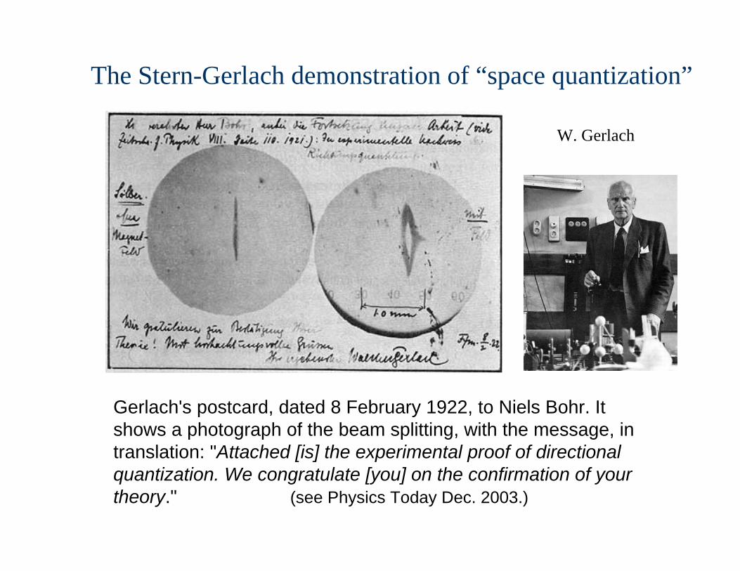
Gerlach's postcard, dated 8 February 1922, to Niels Bohr. It shows a photograph of the beam splitting, with the message, in translation: "Attached [is] the experimental proof of directional quantization. We congratulate [you] on the confirmation of your theory." (see Physics Today Dec. 2003.)
W. Gerlach
The Stern-Gerlach demonstration of “space quantization”
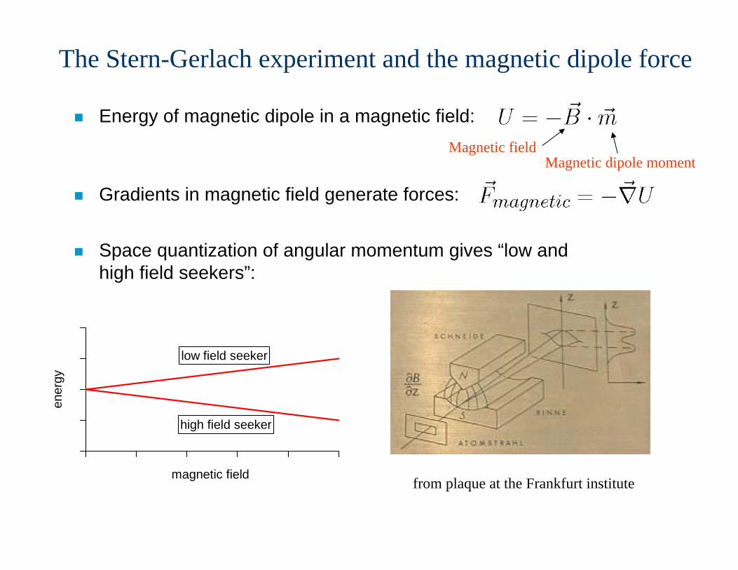
Magnetic dipole moment
The Stern-Gerlach experiment and the magnetic dipole force
Energy of magnetic dipole in a magnetic field:
Gradients in magnetic field generate forces:
Magnetic field
Space quantization of angular momentum gives “low and high field seekers”:
ener
gy
magnetic field
low field seeker
high field seeker
from plaque at the Frankfurt institute
Can the Stern-Gerlach force be used to “trap” atoms?
• review of mechanism of force.
• necessity for laser cooling.
• demonstration.
• miniaturization (atom chips!).
• Rydberg atom surface interactions with atom chips.
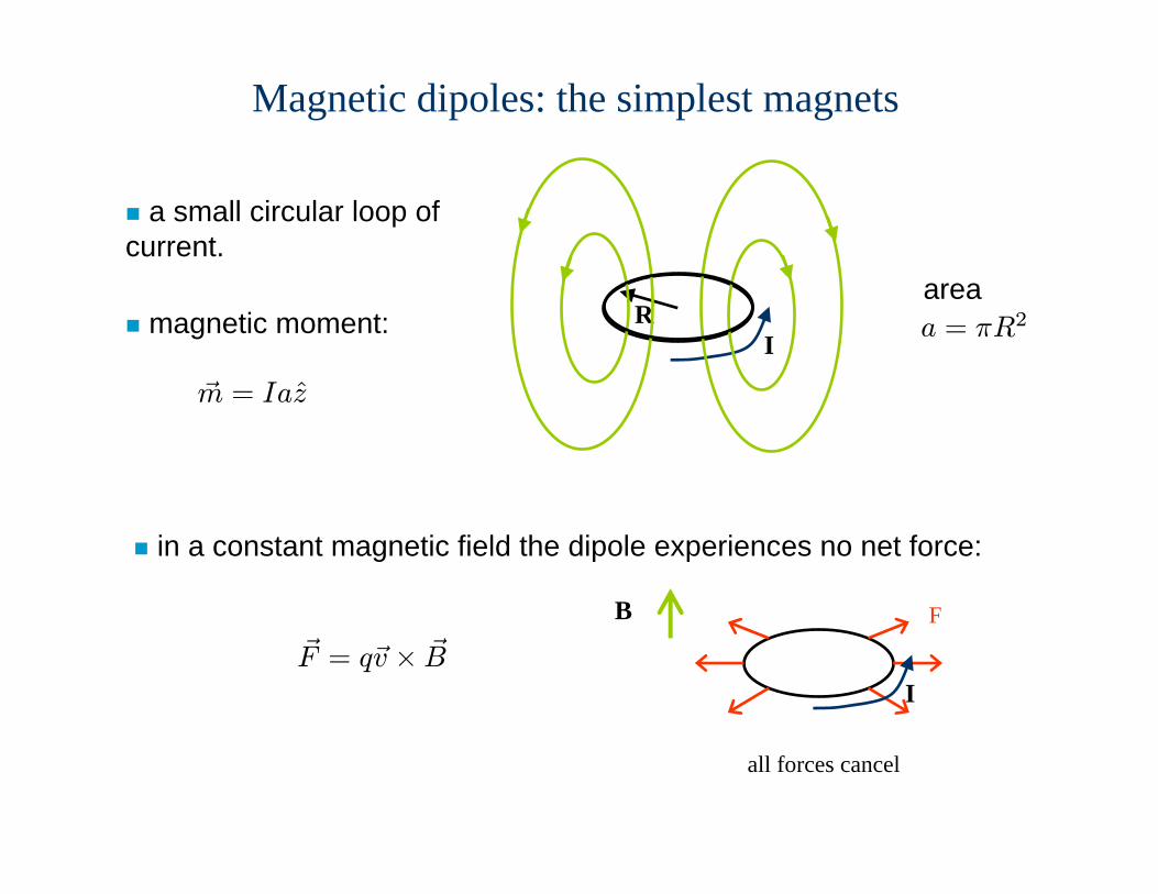
Magnetic dipoles: the simplest magnets
a small circular loop of current.
IR a = πR2
area
in a constant magnetic field the dipole experiences no net force:
~m = Iaz
magnetic moment:
F
all forces cancel
I
B~F = q~v × ~B
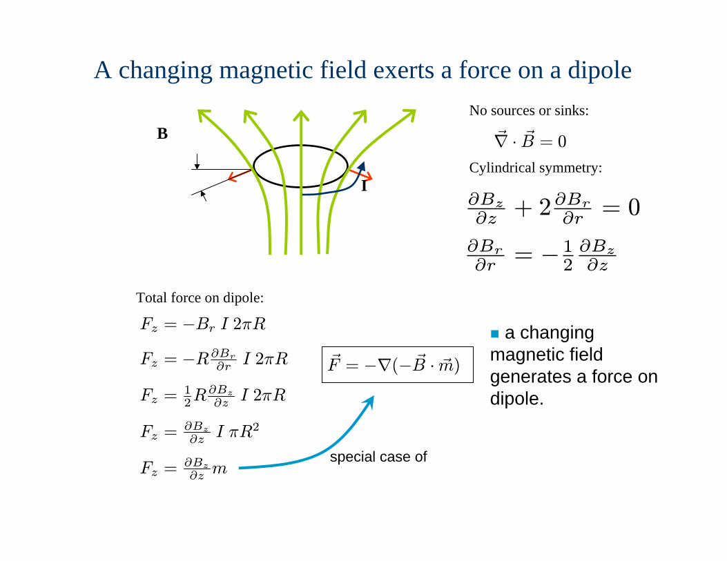
A changing magnetic field exerts a force on a dipole
Cylindrical symmetry:
B
∂Bz∂z
+ 2∂Br∂r
= 0
No sources or sinks:
∂Br∂r
= − 12∂Bz∂z
~∇ · ~B = 0
Total force on dipole:
I
Fz = −Br I 2πR
Fz = −R∂Br
∂r I 2πR
Fz =12R
∂Bz
∂z I 2πR
Fz =∂Bz
∂z I πR2
Fz =∂Bz
∂z m
~F = −∇(− ~B · ~m)a changing
magnetic field generates a force on dipole.
special case of
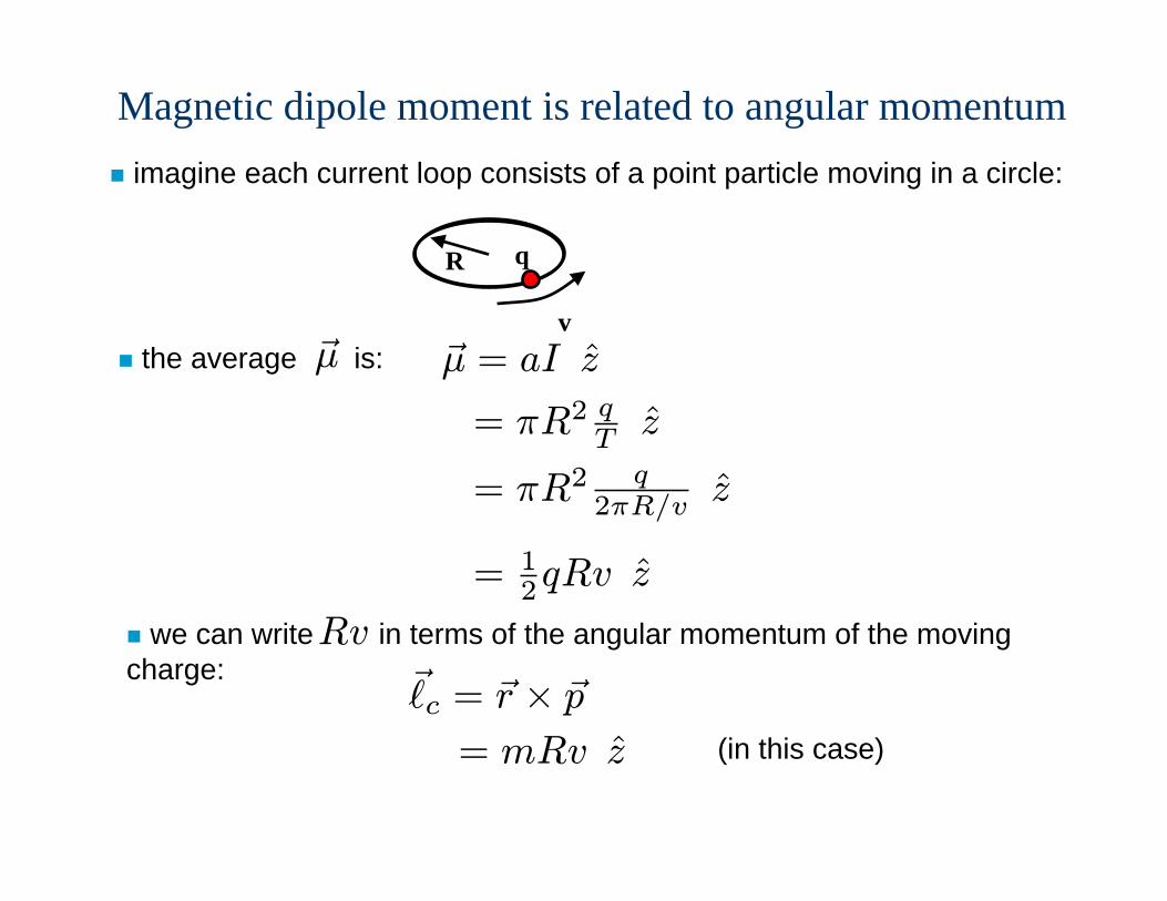
Magnetic dipole moment is related to angular momentumimagine each current loop consists of a point particle moving in a circle:
v
R q
the average is:~μ ~μ = aI z
= πR2 qTz
= πR2 q2πR/v z
= 12qRv z
we can write in terms of the angular momentum of the moving charge:
Rv
~c = ~r × ~p
(in this case)= mRv z
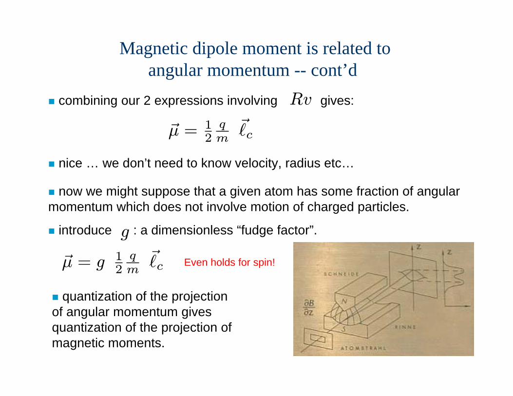
Magnetic dipole moment is related to angular momentum -- cont’d
~μ = 12qm~c
combining our 2 expressions involving gives:Rv
nice … we don’t need to know velocity, radius etc…
now we might suppose that a given atom has some fraction of angular momentum which does not involve motion of charged particles.
introduce : a dimensionless “fudge factor”.
~μ = g 12qm~c
g
quantization of the projection of angular momentum gives quantization of the projection of magnetic moments.
Even holds for spin!
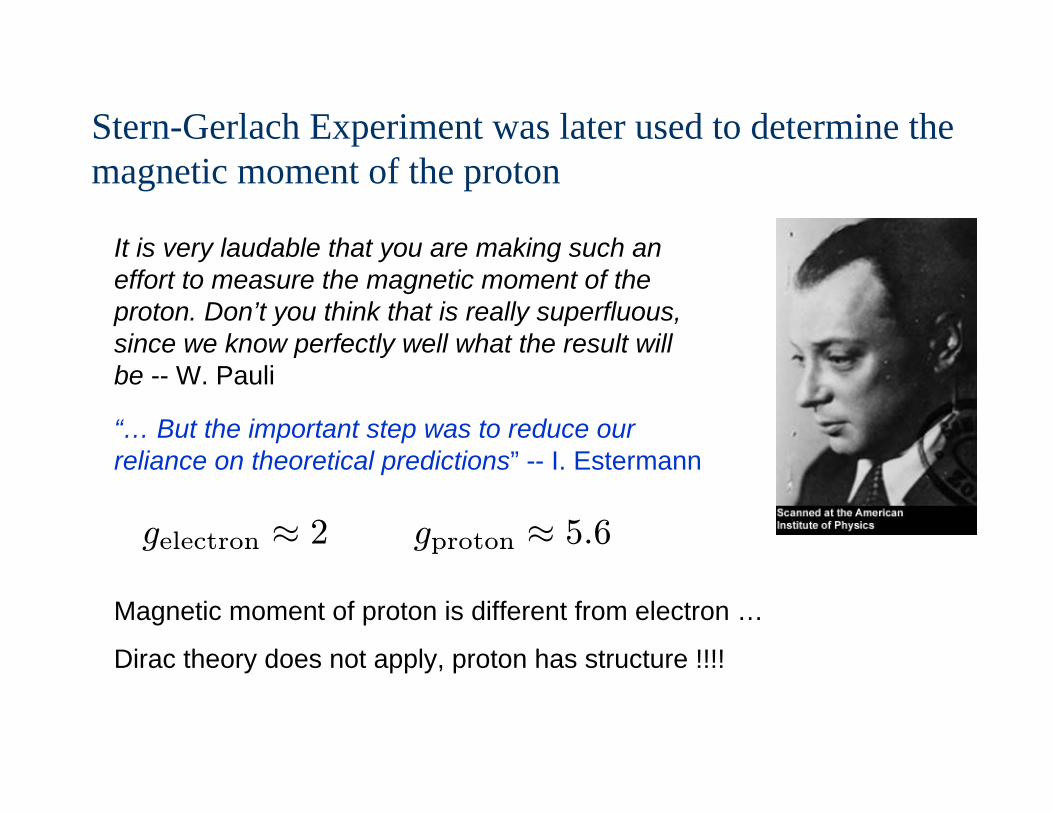
Stern-Gerlach Experiment was later used to determine the magnetic moment of the proton
It is very laudable that you are making such an effort to measure the magnetic moment of the proton. Don’t you think that is really superfluous, since we know perfectly well what the result will be -- W. Pauli
Magnetic moment of proton is different from electron …
Dirac theory does not apply, proton has structure !!!!
“… But the important step was to reduce our reliance on theoretical predictions” -- I. Estermann
gproton ≈ 5.6gelectron ≈ 2
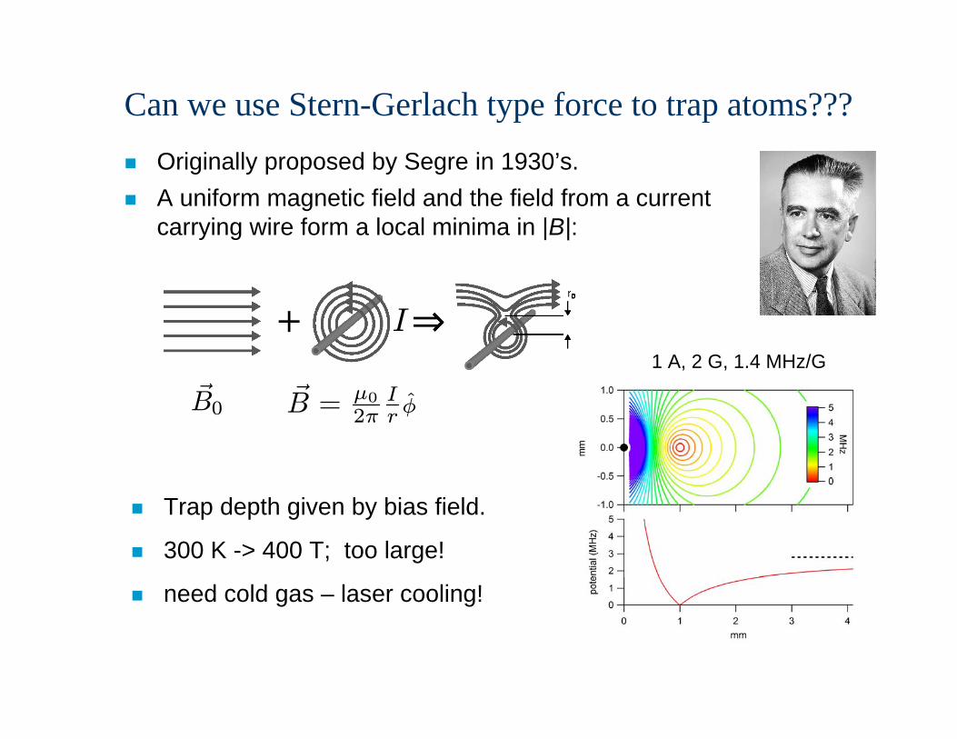
Can we use Stern-Gerlach type force to trap atoms???Originally proposed by Segre in 1930’s.A uniform magnetic field and the field from a current carrying wire form a local minima in |B|:
I
~B0 ~B = μ02π
Ir φ
1 A, 2 G, 1.4 MHz/G
Trap depth given by bias field.
300 K -> 400 T; too large!
need cold gas – laser cooling!
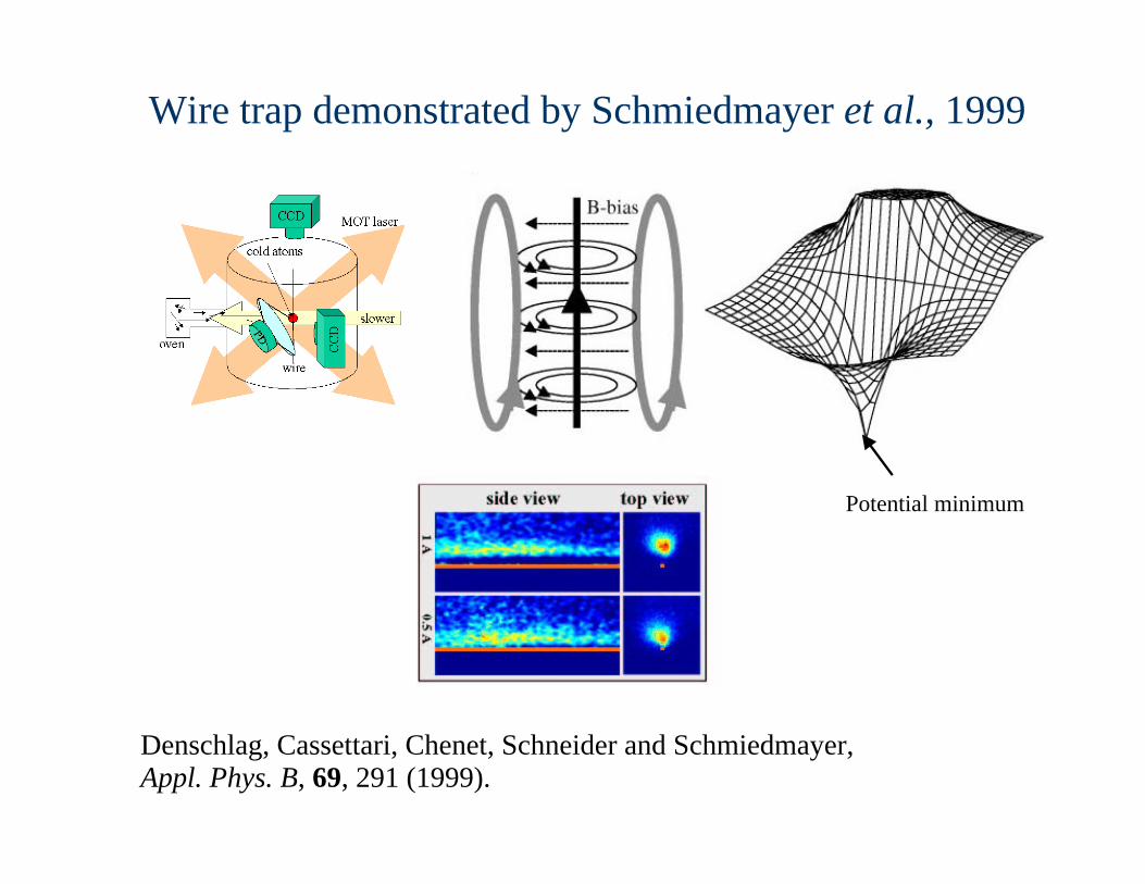
Wire trap demonstrated by Schmiedmayer et al., 1999
Potential minimum
Denschlag, Cassettari, Chenet, Schneider and Schmiedmayer, Appl. Phys. B, 69, 291 (1999).
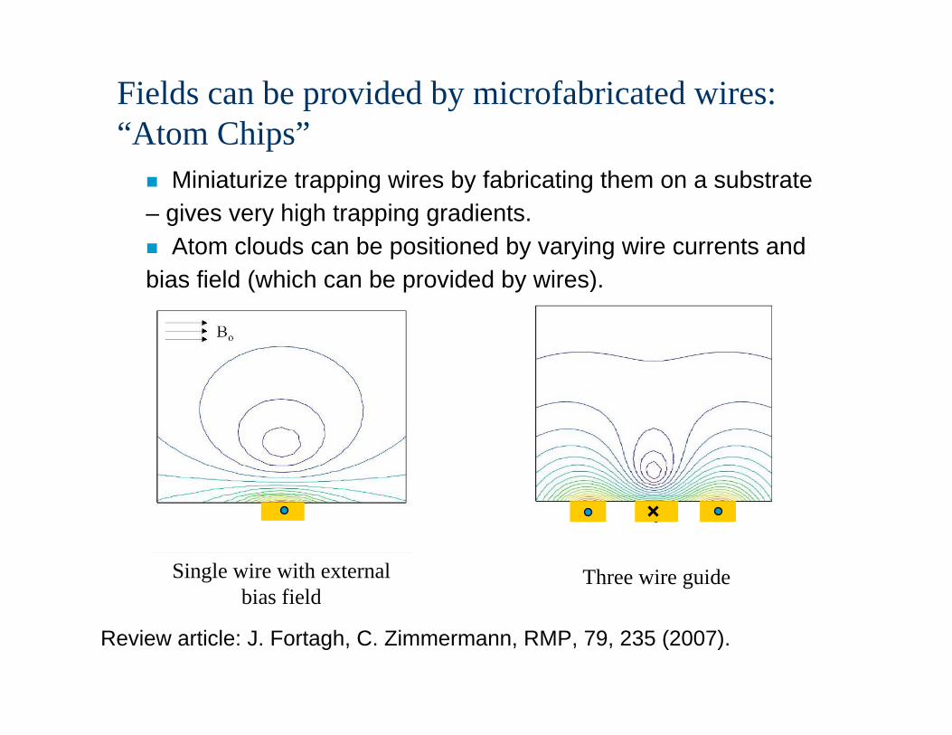
Fields can be provided by microfabricated wires:“Atom Chips”
Single wire with external bias field
Miniaturize trapping wires by fabricating them on a substrate – gives very high trapping gradients.
Atom clouds can be positioned by varying wire currents and bias field (which can be provided by wires).
Three wire guide
Review article: J. Fortagh, C. Zimmermann, RMP, 79, 235 (2007).
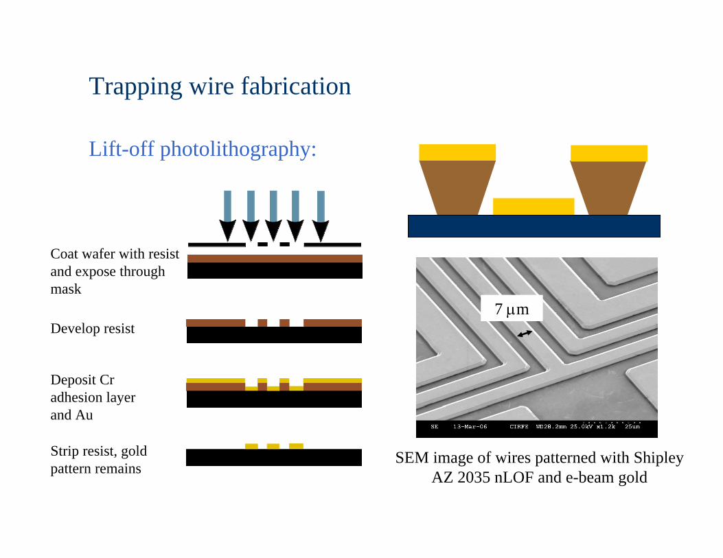
Trapping wire fabrication
Develop resist
Deposit Cr adhesion layer and Au
Strip resist, gold pattern remains
Coat wafer with resist and expose through mask
SEM image of wires patterned with ShipleyAZ 2035 nLOF and e-beam gold
Lift-off photolithography:
7 μm
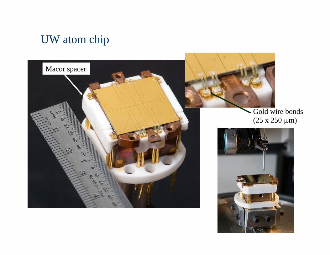
Gold wire bonds (25 x 250 μm)
UW atom chip
Macor spacer
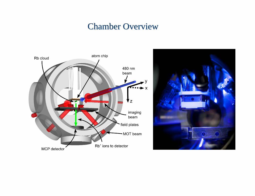
Chamber OverviewChamber Overview
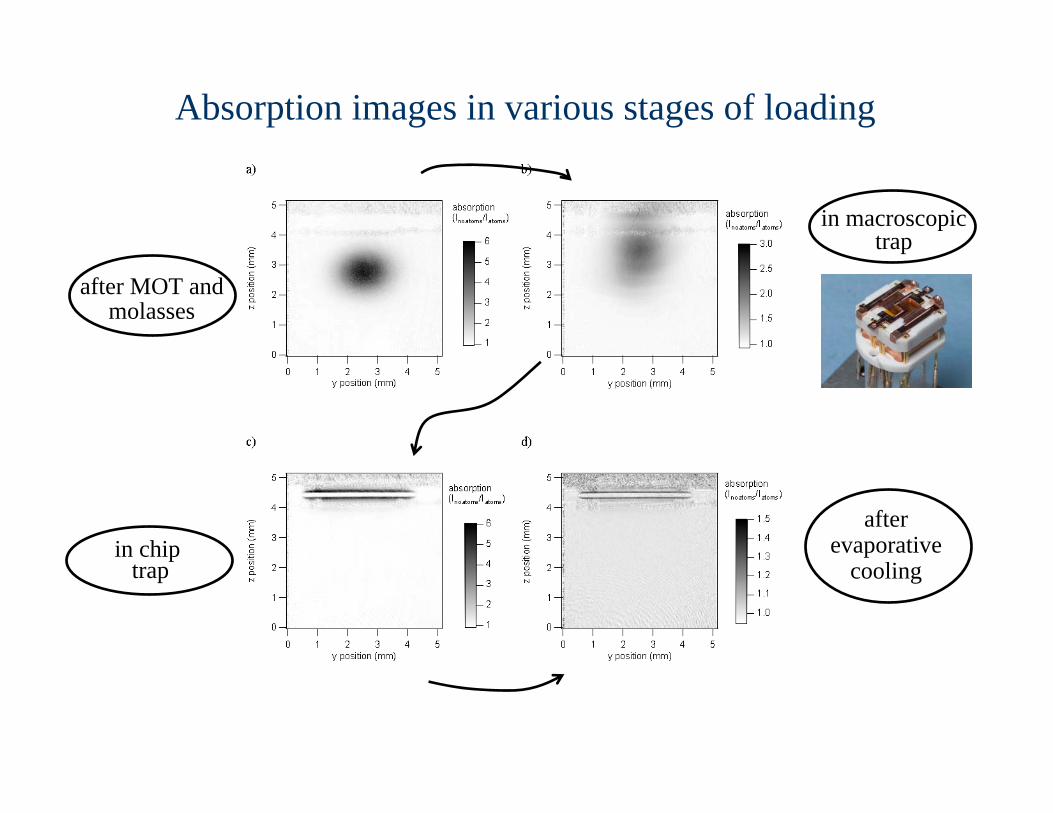
Absorption images in various stages of loading
after MOT andmolasses
in macroscopic trap
in chip trap
afterevaporative
cooling
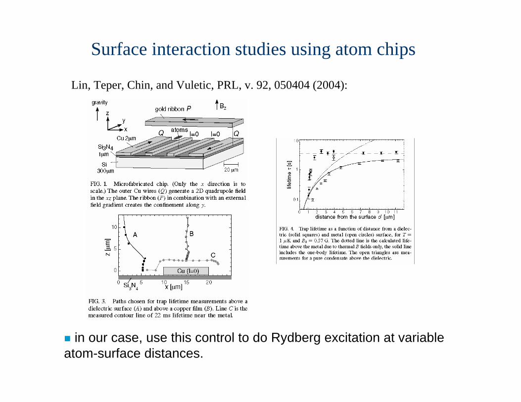
Surface interaction studies using atom chips
Lin, Teper, Chin, and Vuletic, PRL, v. 92, 050404 (2004):
in our case, use this control to do Rydberg excitation at variable atom-surface distances.
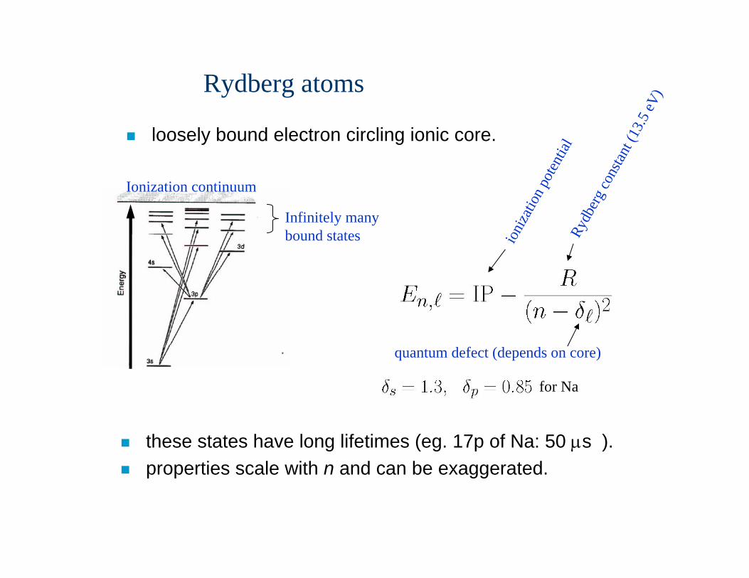
Rydberg atoms
loosely bound electron circling ionic core.
Ionization continuum
Infinitely many bound states
these states have long lifetimes (eg. 17p of Na: 50 μs ).properties scale with n and can be exaggerated.
for Na
ioni
zatio
n pot
entia
l
quantum defect (depends on core)
Rydb
erg c
onsta
nt (1
3.5 eV
)
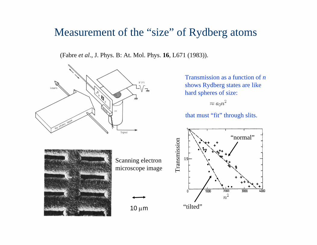
Measurement of the “size” of Rydberg atoms
(Fabre et al., J. Phys. B: At. Mol. Phys. 16, L671 (1983)).
Scanning electron microscope image
“tilted”
“normal”
Transmission as a function of nshows Rydberg states are like hard spheres of size:
that must “fit” through slits.
Tran
smis
sion
10 μm
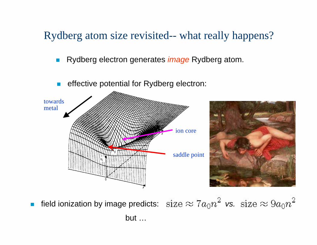
Rydberg atom size revisited-- what really happens?
Rydberg electron generates image Rydberg atom.
towardsmetal
effective potential for Rydberg electron:
ion core
saddle point
field ionization by image predicts: vs.
but …
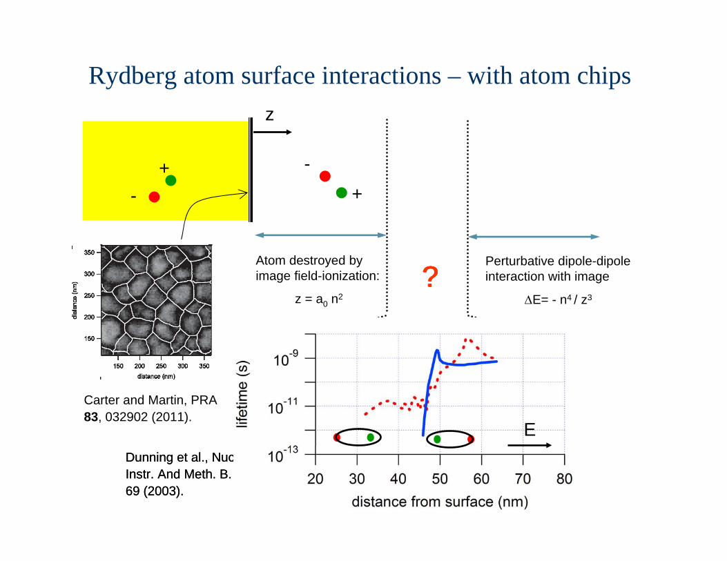
Rydberg atom surface interactions – with atom chipsz
+-
-+
?
Dunning et al., Nucl.Instr. And Meth. B. 203,69 (2003).
Carter and Martin, PRA83, 032902 (2011).
Atom destroyed by image field-ionization:
z = a0 n2
Perturbative dipole-dipole interaction with image
ΔE= - n4 / z3
E
n=14
?
E
?
EDunning et al., Nucl.Instr. And Meth. B. 203,69 (2003).
?
E
O. Cherry, R. Al-Dahleh (CIRFE Group)
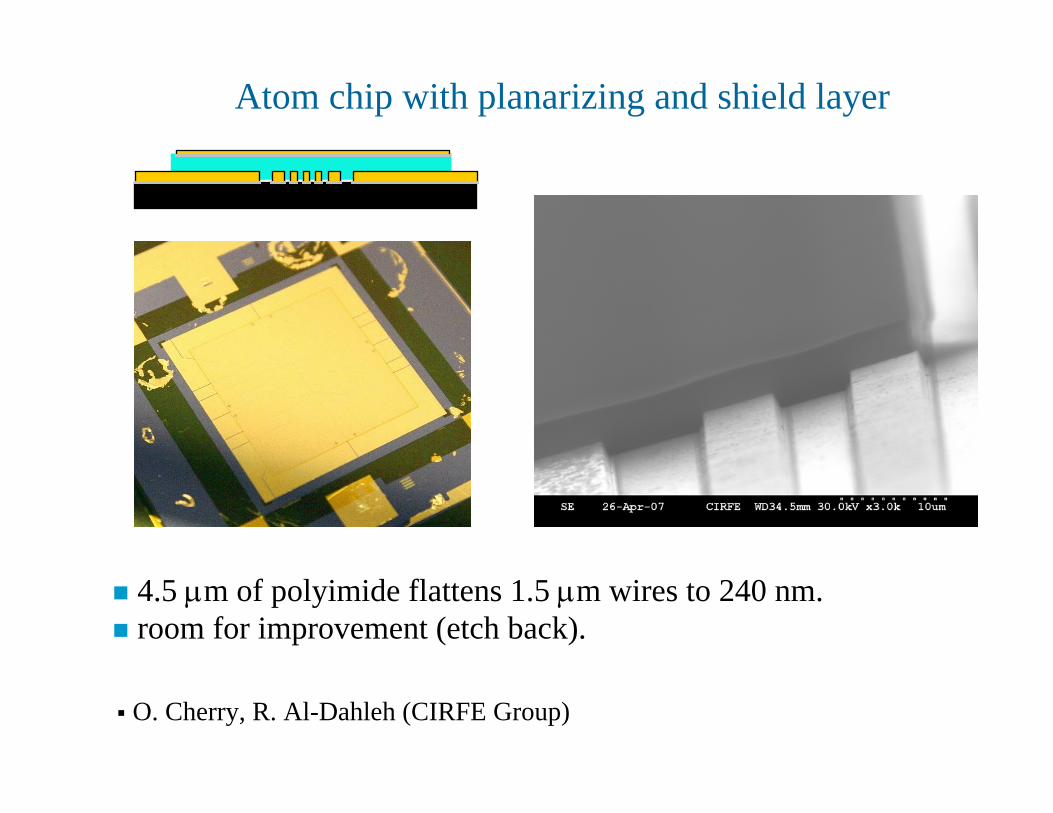
Atom chip with planarizing and shield layer
4.5 μm of polyimide flattens 1.5 μm wires to 240 nm.room for improvement (etch back).
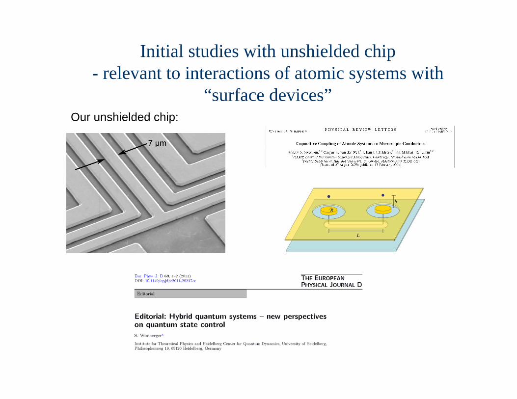
Initial studies with unshielded chip- relevant to interactions of atomic systems with
“surface devices”Our unshielded chip:
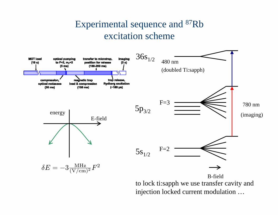
Experimental sequence and 87Rb excitation scheme
5s1/2
5p3/2
36s1/2
F=2
F=3 780 nm
(imaging)
480 nm (doubled Ti:sapph)
B-fieldto lock ti:sapph we use transfer cavity and injection locked current modulation …
E-field
δE = −3 MHz(V/cm)2F
2
energy
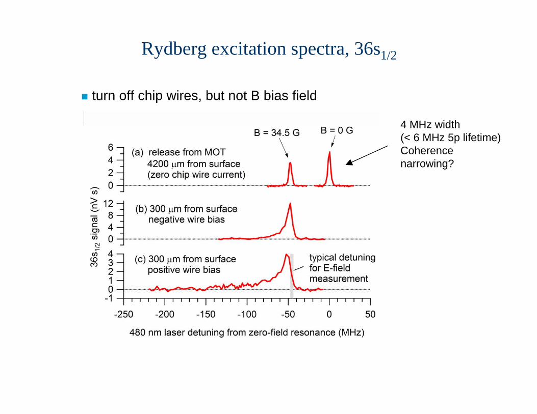
Rydberg excitation spectra, 36s1/2
turn off chip wires, but not B bias field
4 MHz width(< 6 MHz 5p lifetime)Coherence narrowing?
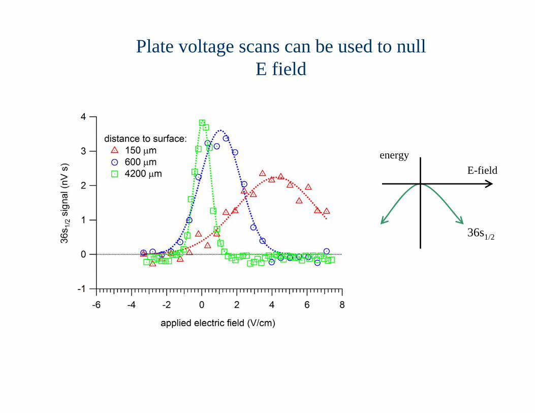
Plate voltage scans can be used to null E field
E-field
36s1/2
energy
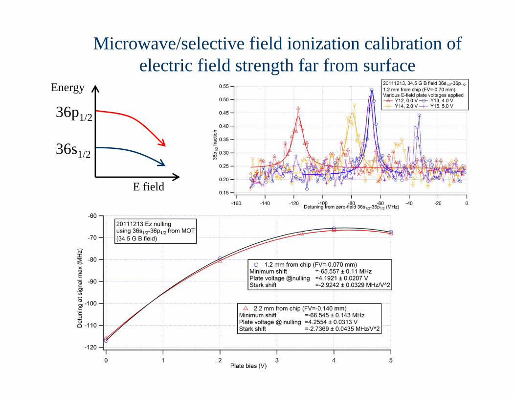
Microwave/selective field ionization calibration of electric field strength far from surface
36s1/2
36p1/2
E field
Energy
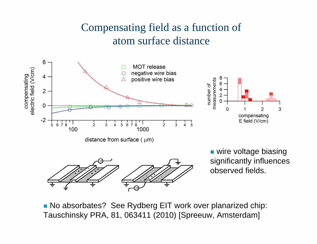
Compensating field as a function of atom surface distance
No absorbates? See Rydberg EIT work over planarized chip: Tauschinsky PRA, 81, 063411 (2010) [Spreeuw, Amsterdam]
wire voltage biasing significantly influences observed fields.
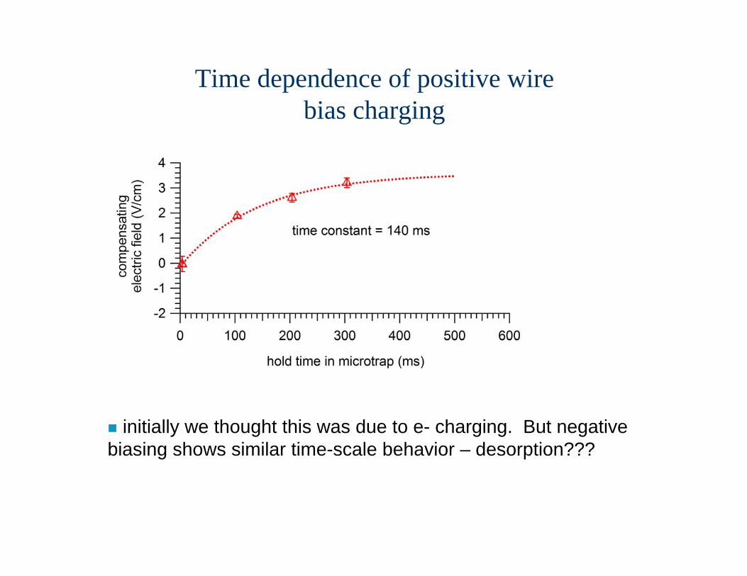
Time dependence of positive wire bias charging
initially we thought this was due to e- charging. But negative biasing shows similar time-scale behavior – desorption???
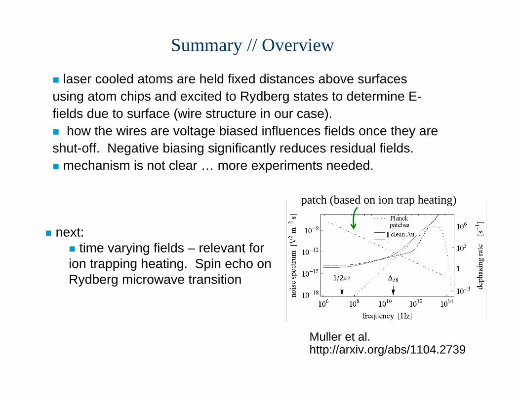
Summary // Overview
laser cooled atoms are held fixed distances above surfaces using atom chips and excited to Rydberg states to determine E-fields due to surface (wire structure in our case).
how the wires are voltage biased influences fields once they are shut-off. Negative biasing significantly reduces residual fields.
mechanism is not clear … more experiments needed.
next: time varying fields – relevant for
ion trapping heating. Spin echo on Rydberg microwave transition
Muller et al.http://arxiv.org/abs/1104.2739
patch (based on ion trap heating)
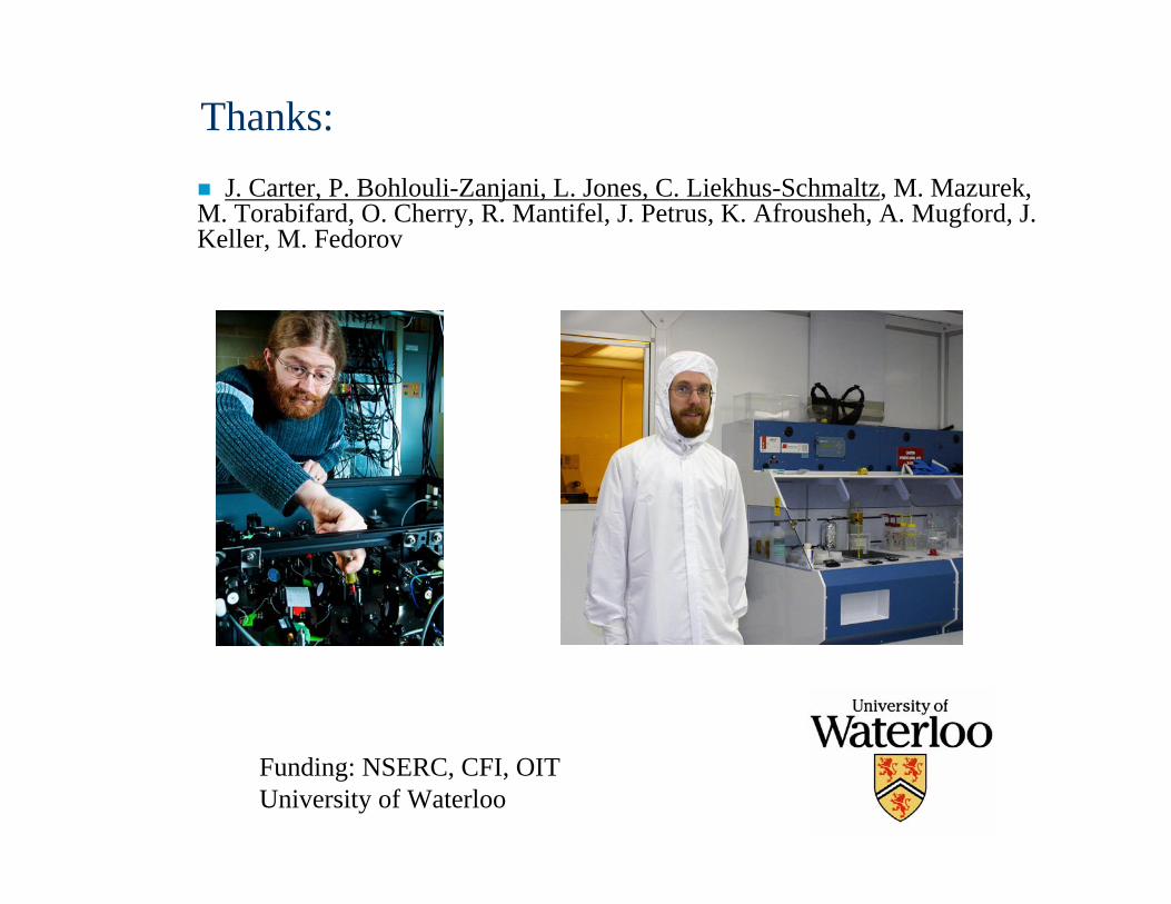
Thanks:J. Carter, P. Bohlouli-Zanjani, L. Jones, C. Liekhus-Schmaltz, M. Mazurek,
M. Torabifard, O. Cherry, R. Mantifel, J. Petrus, K. Afrousheh, A. Mugford, J. Keller, M. Fedorov
Funding: NSERC, CFI, OITUniversity of Waterloo
Apparatus
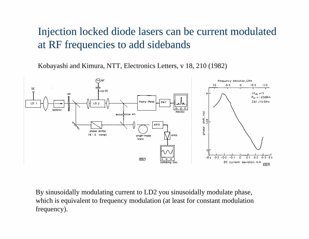
Injection locked diode lasers can be current modulated at RF frequencies to add sidebands
Kobayashi and Kimura, NTT, Electronics Letters, v 18, 210 (1982)
By sinusoidally modulating current to LD2 you sinusoidally modulate phase, which is equivalent to frequency modulation (at least for constant modulation frequency).
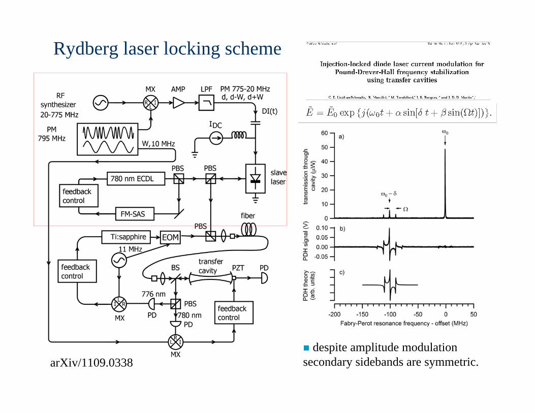
Rydberg laser locking scheme
arXiv/1109.0338despite amplitude modulation
secondary sidebands are symmetric.