eindhoven university of technology bachelor multi-layer ... · preface this report is a part of my...
TRANSCRIPT
Eindhoven University of Technology
BACHELOR
Multi-layer barriers on polymer (PEN) substrate
analysis of thin Al2O3 ALD films on fast deposited SiOx buffer layers
Schalken, J.R.G.
Award date:2012
Link to publication
DisclaimerThis document contains a student thesis (bachelor's or master's), as authored by a student at Eindhoven University of Technology. Studenttheses are made available in the TU/e repository upon obtaining the required degree. The grade received is not published on the documentas presented in the repository. The required complexity or quality of research of student theses may vary by program, and the requiredminimum study period may vary in duration.
General rightsCopyright and moral rights for the publications made accessible in the public portal are retained by the authors and/or other copyright ownersand it is a condition of accessing publications that users recognise and abide by the legal requirements associated with these rights.
• Users may download and print one copy of any publication from the public portal for the purpose of private study or research. • You may not further distribute the material or use it for any profit-making activity or commercial gain
Multi-layer barriers on polymer (PEN) substrate:
Analysis of thin Al2O3 ALD �lms on
fast deposited SiOx bu�er layers
Jean-Paul Schalken (0595457)
Under supervision of:
Hindrik de Vries and
Mariadriana Creatore
November 18, 2012

�
1
Preface
This report is a part of my master's degree program in Applied Physics at Eindhoven
University. An internship at a university abroad or at a company is a part of the master's
program, in order to apply technical en scienti�c knowledge in a research environment,
other than at our university. I'm very glad that Fuji�lm gave me the oppurtunity to do an
internship. In this way, I can experience the di�erences between research in an academic
environment and at a company like Fuji�lm. This can help me with my decisions further in
my career. Therefore, I want to thank Hindrik and Adriana for providing me this option.
Next to that, I want to thank Hindrik, Sergey and Adriana for their discussions and
feedback. Of course I also want to thank Bernadette, Bruno, Marco and Rinie for their
technical support, as well as all their other help. At last, I want to thank the people from
Eindhoven University which technically supported me, thank you Cristian and Wytze.
2

�
3
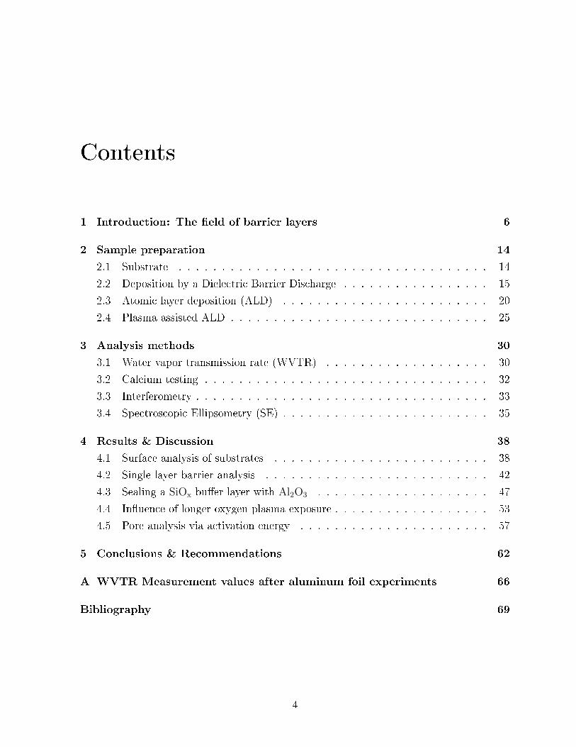
Contents
1 Introduction: The �eld of barrier layers 6
2 Sample preparation 14
2.1 Substrate . . . . . . . . . . . . . . . . . . . . . . . . . . . . . . . . . . . . 14
2.2 Deposition by a Dielectric Barrier Discharge . . . . . . . . . . . . . . . . . 15
2.3 Atomic layer deposition (ALD) . . . . . . . . . . . . . . . . . . . . . . . . 20
2.4 Plasma assisted ALD . . . . . . . . . . . . . . . . . . . . . . . . . . . . . . 25
3 Analysis methods 30
3.1 Water vapor transmission rate (WVTR) . . . . . . . . . . . . . . . . . . . 30
3.2 Calcium testing . . . . . . . . . . . . . . . . . . . . . . . . . . . . . . . . . 32
3.3 Interferometry . . . . . . . . . . . . . . . . . . . . . . . . . . . . . . . . . . 33
3.4 Spectroscopic Ellipsometry (SE) . . . . . . . . . . . . . . . . . . . . . . . . 35
4 Results & Discussion 38
4.1 Surface analysis of substrates . . . . . . . . . . . . . . . . . . . . . . . . . 38
4.2 Single layer barrier analysis . . . . . . . . . . . . . . . . . . . . . . . . . . 42
4.3 Sealing a SiOx bu�er layer with Al2O3 . . . . . . . . . . . . . . . . . . . . 47
4.4 In�uence of longer oxygen plasma exposure . . . . . . . . . . . . . . . . . . 53
4.5 Pore analysis via activation energy . . . . . . . . . . . . . . . . . . . . . . 57
5 Conclusions & Recommendations 62
A WVTR Measurement values after aluminum foil experiments 66
Bibliography 69
4

�
5
Chapter 1
Introduction: The �eld of barrier layers
In the challenge to improve electronic devices, steps are made in trying to produce cheaper
electronics with better properties. A major cost reduction can be achieved by the roll-to-
roll production of organic electronics on polymer substrates. Devices which can be pro-
duced in a roll-to-roll setup are organic solar cells, organic light-emitting diodes (OLED)
as well as inorganic CIGS photovoltaics (thin �lms of copper indium gallium diselenide).
LED technology is an established technology for lighting, as well as that it is often used as
backlight for LCD television screens. Organic LED technology is an emerging technology
that allows the production of �exible displays.[20] A problem when working with organic
material, however, is that devices degrade under the in�uence of water vapor.[21] This sus-
ceptibility to moisture is induced by the metal cathodes, which get oxidized by water vapor
and oxygen, leading to a delamination of the underlying organic layer.[21] Non-emissive
black spots are resulting at the surface of the OLED. This oxidation process should be
counteracted by the deposition of a barrier layer. Where glass or metal substrates have ef-
fective barrier properties themselves, polymer substrates require a barrier for water vapor
and oxygen permeation, which should protect the device from degradation.[20] It is esti-
mated that the maximum permeation through a barrier should be around 1× 10⁻⁶g/m2·day
for water vapor (WVTR) and 10−5−10−3 cm3/m2·day (OTR), resulting in an OLED lifetime
of > 10000 h.[20] This is the time, that is needed to degrade the reactive cathode of the
OLED by water vapor and oxygen.
There are several techniques and materials researched to deposit barrier layers. How-
ever, only a few of them work as e�ective barriers for water vapor and for oxygen. Nowa-
days, lots of research is done in the deposition of barrier layers by atomic layer deposition
(ALD). ALD is known for the ability to deposit dense, conformal layers with a low defect
density.[9] This is a good technique to deposit barrier layers, especially because the per-
6

meation through these kind of barrier layers is mainly driven by defects.[6] The principle
of the ALD technique as well as its advantages and disadvantages will be more extensively
discussed in sect. (2.3).
Since deposition of Al2O3 by ALD is conformal and delivers a dense �lm, there is of-
ten research performed using these layers as barriers layers. Carcia et al. also did some
interesting research depositing Al2O3 barriers, which resulted in an estimated barrier of
6× 10⁻⁶g/m2·day at standard conditions of 23 °C and 50 % relative humidity (RH).[4] This
was derived from experiments at elevated temperatures (38 °C and 60 °C): via these re-
sults, the apparent activation energy (∆Eact) could be determined and the WVTR could
be extrapolated to room temperature. The measurements were done on a 25 nm, by ALD
deposited, barrier layer of Al2O3, deposited on a PEN substrate (polyethylene naphtha-
late), while the ALD process was performed at 120 °C, using trimethylaluminum (TMA)
and water vapor as precursors. In their research, they mention the importance of the
cleaning process: �The cleanliness and surface chemistry of the polymer were critical for
achieving thin, defect free �lms with ultra low permeability.� Therefore they rinsed the
samples before loading them into an ALD reactor via a laminar �ow hood, operating at
class 100 cleanroom conditions.[4] In a later publication, they explained more about their
cleaning procedure.[3]
Also Keuning et al. deposited Al2O3 barrier layers by ALD. In their ALD process,
however, they used an oxygen plasma[12], instead of water vapor to oxidize the Al2O3
�lm, opening the possibility to deposit at lower temperatures: 25 °C. Due to this low
temperature, they used a plasma exposure time of 4 s, to keep the carbon content low.
With these conditions, they obtained an intrinsic barrier performance (WVTR) of ≤2× 10⁻⁶g/m2·day for 20− 40 nm barrier layers at 20 °C and 50 % RH.
Both Carcia et al. and Keuning et al. characterized the barrier performance using a
calcium test (Ca test). This test method o�ers the possibility to measure the intrinsic
WVTR in between the defects, excluding water vapor permeation through pinholes (as
used in this research project and by Keuning et al.), but a Ca test can also be used to
determine the extrinsic WVTR (as used by Carcia et al.). This is shown in �g. (1.1). The
di�erence between the two setups is the epoxy layer, which is used at the setup of Carcia
et al. This epoxy layer allows the water vapor, which has permeated through the barrier
�lm, to di�use all over the di�erent calcium spots. This is in contrast to our own setup
in which the water vapor, after it has permeated through the barrier, directly oxydaizes
the calcium at the speci�c spot of the pores or pinholes. The Ca test is explained more
extensively in sect. (3.2).
The deposition rate of ALD, however, is relatively low. Therefore, until recent, it
7

Figure 1.1: Setup of the Ca test for the determination of the intrinsic WVTR (left) andthe extrinsic WVTR (right, [4] (edited)). The bottom �gures are examples of the speci�cCa tests. White dots are present in our setup due to the direct contact between the barrierlayer and the calcium, while an overal grey area is shown in the results of Carcia et al.[4]
was believed that good barrier �lms at high deposition rate could only be achieved by
a low pressure PECVD process. However, establishing roll-to-roll high volume PECVD
deposition of barrier �lms in vacuum is not a prerequisite. An alternative to low pressure
PECVD is to deposit barrier layers via a dielectric barrier discharge (DBD, sect. (2.2)),
since it can easily be implemented in a roll-to-roll production system. Using the so-called
atmospheric pressure, glow discharge plasma (APGD plasma), SiOx �lms with an extrinsic
barrier of < 5×10⁻³g/m2·day were demonstrated.[25] Fuji�lm and TU/e already gained a lot
of knowledge on this DBD.[1, 2, 25, 26, 29, 30, 31, 32] A remarkable result in this project
was that the barrier layers deposited by the APGD plasma have a WVTR which is strongly
dependent on the barrier thickness according WVTR ∝ t−3.[8] This typical behavior is
shown in �g. (1.2). In this �gure the WVTR measured by Fuji�lm is compared to the
results of ideal laminate theory (ILT,[27])
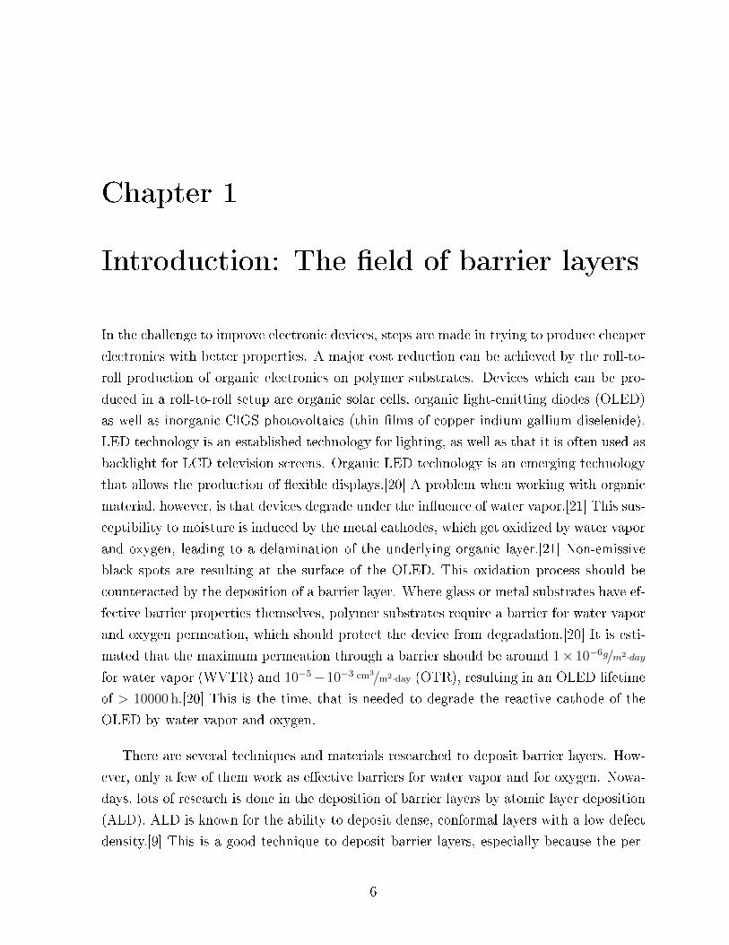
Three types of permeation through the SiOx can be distinguished.[27] Permeation
can take place via macro-defects (md, size> 1 nm), nano-defects (nd, size= 0.3− 1 nm) or
lattice interstices (la, size< 0.3 nm) as shown in �g. (1.3). Since the size of a H2O molecule
is 0.33 nm, it can be assumed that the permeation through lattice interstices is negligible.
8

Figure 1.2: The in�uence of the thickness of the barrier layer on the WVTR. The resultsof research performed at Fuji�lm are shown and compared to results of ILT.
It is shown that some permeation through the lattice is possible, though many orders
of magnitude lower than the permeation via nano-defects.[7] Furthermore, it can be said
that well deposited barriers are characterized by the fact that there are no macro-defects
found, leaving the only transport mechanism to be through nano-scale defects.[6] These
nano-defects form columnar molecular size pathways at the edges of grain boundaries, via
which H2O and O2 can di�use through a SiOx barrier, to reach the polymer.[6]
In principle, the permeation through a barrier can be described by some simple equa-
tions from ILT, depending on the permeation through the individual layers
PILT =
(φpolymerPpolymer
+φSiOx
PSiOx
)−1
using φpolymer = tpolymer/t and φSiOx = tSiOx/t (1.1)
And since PSiOx/φSiOx � Ppolymer/φpolymer, this can be simpli�ed to:
Pbarrier,ILT ≈PSiOx
φSiOx
(1.2)
From this equation, it can be concluded that the WVTR should be proportional to the
inverse of the thickness of the barrier layer (WV TR ∝ t−1) , which is in contrast to the
results found by Fuji�lm, mentioned before (WVTR ∝ t−3). There can be several reasons
for this discrepancy. The most important reason is that ILT assumes a homogeneous
uniform barrier. However - as already shown before - this is not the case. The transport
9
Figure 1.3: Three types of permeation, as proposed by A.P. Roberts et. al.[27]
of water vapor through the barrier is mainly through defects in the material. The average
number and size of these defects, depends on the deposition method and on the process
conditions, but also on the thickness of the layer, as thicker layers have less defects per unit
volume than thinner layers.[27] So the pore structure of the barrier, as well as the surface
roughness can have a large in�uence on the barrier performance. Furthermore, water
vapor will interact with the SiOx surface, forming SiOH groups at dangling Si−O− and
Si− bonds.[6] The H2O molecules can get adsorbed at the surface of the nano-sized pores,
which requires energy to again remove them, as well as that these adsorbed molecules
tend to hinder the permeation through these pores, simply because the pores get thinner.
However, this e�ect of adsorbing water vapor at the edges of the pores is said to be less
important for SiOx, compared to AlOx or SiNx, because the binding energy for SiOx
is much lower.[8] At last, it can be possible that the SiOx barrier is damaged by the
permeation of the water vapor, e.g. cracks can be created or enlarged.[6]
Furthermore, from eq. (1.1) it is also possible to derive a multi-layer model for perme-
ation through a barrier ((1.3),[3]). This is important when producing a barrier consisting
of multiple layers. When using multiple layers a mismatch between the various pores of
these layers can result in a much lower permeability of the barrier, since the permeat-
ing gas is forced to (partly) di�use through the intrinsic material, instead of through the
pores.[33] For a single layer barrier, di�usion through pores would be the main driving
force for permeation. A barrier of intrinsic material - where the permeant should di�use
via lattice interstices - is much better, resulting in a lower permeation.
10
1/Pbarrier = 1/Ppolymer + 1/Player1 + 1/Player2 (1.3)
At last it, it is shown that the type of permeation (via macro-defects, nano-defects
or lattice interstices) can be related to the activation energy of the barrier (∆Eact). For
a speci�c permeant, the activation energy increases if the barrier is deposited with less
defects.[33] For oxygen permeation, ∆Eact can vary from ±30 kJ/mol for a weak barrier with
lots of large defects (same as substrate), up to ±100 kJ/mol for ideal SiOx where permeation
is only possible via lattice interstices.[33] For water vapor permeation on the other hand,
∆Eact varies from 50−55 kJ/mol for poor barriers (same as PET substrate) up to ±84 kJ/mol
for ideal, silica glass barriers.[6, 27] This activation energy relates the permeation (Π in
[mol/m2·s·atm]) to the temperature via:[33]
Π = Π0 exp (−∆Eact/RT) (1.4)
in which Π0 is a constant and R the ideal gas constant. From this the activation energy
can be determined:
∆Eact = −R ∂
∂ (1/T)ln (Π/Π0) (1.5)
Analysis of the pores structure are important in this project. Since in this project
analysis are done to increase the deposition rate of SiOx barriers while sustaining the
barrier quality; the WVTR should remain the same, or even decrease. In general, an
increase of the deposition rate results in worse SiOx barrier �lms. The barrier structure
becomes more porous, which enhance moisture permeation. Since water vapor permeation
is mainly through interconnected nano-pores, the idea is to deposit a thin �lm on top of this
SiOx layer, which is able to seal this percolated structure. Atomic layer deposition (ALD,
sec. (2.3)) is used for this, since it is a conformal and defect free deposition technique.
When depositing a thin layer of Al2O3 (0.5 − 10 nm) by ALD on top of the SiOx layer -
deposited by DBD - a good barrier may be deposited, while the deposition process can
be performed much faster. This research focuses on the option to sustain low moisture
permeation through HDR SiOx layer by sealing this bu�er layer with a thin Al2O3 layer.
This is also depicted in �g. (1.2).
For example the minimum thickness of the Al2O3 layer has been investigated to main-
tain a good barrier quality. Furthermore, the interaction between the layers deposited by
CVD and ALD is analyzed; are the layers intermixing and in what kind of way? Also the
in�uence of the amount of carbon in the layer is researched. If the Al2O3 layer is deposited
11
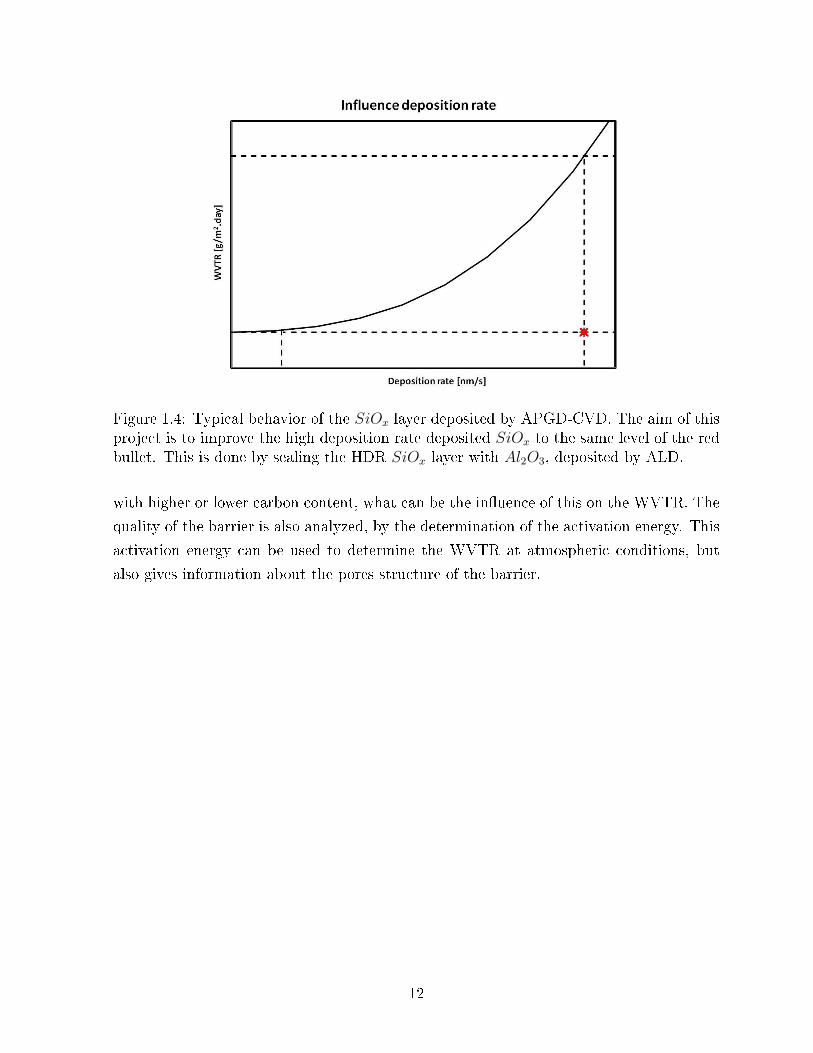
Figure 1.4: Typical behavior of the SiOx layer deposited by APGD-CVD. The aim of thisproject is to improve the high deposition rate deposited SiOx to the same level of the redbullet. This is done by sealing the HDR SiOx layer with Al2O3, deposited by ALD.
with higher or lower carbon content, what can be the in�uence of this on the WVTR. The
quality of the barrier is also analyzed, by the determination of the activation energy. This
activation energy can be used to determine the WVTR at atmospheric conditions, but
also gives information about the pores structure of the barrier.
12

�
13
Chapter 2
Sample preparation
The samples for this research project are prepared on �exible substrates (PEN or PET, see
sec. (2.1)). A SiOx �lm (∼ 70 nm) is deposited on these substrates using chemical vapor
deposition via an atmospheric pressure glow discharge (APGD-CVD), which is also called
dielectric barrier discharge (DBD, sec. (2.2)). Subsequently the SiOx layer is sealed by a
thin layer of Al2O3 (0.5− 10 nm) using plasma assisted atomic layer deposition (PA-ALD,
sec. (2.4)). The APGD-CVD and ALD deposition techniques, as well as background on
the used substrates is provided in this chapter. Furthermore, standard thermal ALD is
explained (see sec. (2.3)), since this is the basic principle of PA-ALD.
2.1 Substrate
The idea is that the barriers are protecting products like �exible electronics against dete-
rioration by water vapor. Therefore, there are several requirements for the substrate. The
most obvious properties are �exibility, transparency and robustness, but next to that, it is
also desired that the substrate has a low coe�cient of thermal expansion (CTE) amongst
others, so that it can be easily processable at di�erent temperatures. A high CTE may
promote cracks in the barrier material, which would drastically increase the water vapor
transmission rate (WVTR).
There are several substrates meeting these requirements. Research in this kind of �eld
is often performed on PEN, poly(ethylene 2,6-naphthalate).[3, 25] The structure formula
for PEN is shown in �g. (2.1). This organic polymer, from DuPont Teijin Films, is heat
stabilized and it has an anti-blocking layer on the back. The anti-blocking layer is desired
when winding up the polymer, taking care that the two sides of the polymer do not stick
to each other, creating cracks already before deposition. The total thickness of the PEN
substrate is 100µm.
14

Figure 2.1: Structure formula of PEN [poly(ethylene 2,6-naphthalate)]
Figure 2.2: Structure formula of PET [poly(ethylene teraphthalate)]
Another optional material, which can be used as a substrate for the analysis of the
barriers is PET, poly(ethylene teraphthalate). This is even more known, because of the
worldwide use in packaging or drinking bottles. It is cheaper than PEN, but the properties
are not as good as for PEN. PET is also be delivered with an anti-blocking layer on the
back.
PEN and PET can also be delivered with a transparent planarizing layer (a TP layer).
With the TP layer the surface becomes smoother and has fewer defects. This PEN/TP (or
PET/TP) surface is protected by a so called inter leaf foil (ILF), in order to protect the
substrate when winding it up or unwinding it later on. The ILF is removed just before the
deposition starts, keeping the substrate surface as clean as possible. In that way, the ILF
reduces the probability of particle contamination during the web handling, otherwise more
defects are generated. Defects are the major permeation mechanism in the permeation of
water vapor or oxygen through the barrier[27], so it is important to prevent the surface
from all kinds of particles, which could create defects.[4]
Since the TP layer is a product of Fuji�lm and it is not exactly known, the surface
properties of this organic planarizing layer are investigated using interferometry. These
results are compared to the bare PEN and bare PET layers (results shown in sec. (4.1)).
This is done by interferometry. The working of interferometry will be explained in sec.
(3.3).
2.2 Deposition by a Dielectric Barrier Discharge
When industrially producing barriers for �exible electronics, it is desired to combine the
production of coatings for large area substrates together with reasonable low production
15

Figure 2.3: a) Standard �lamentary discharge, b) Uniform di�usive atmospheric pressureglow discharge.[32]
costs. In this view , a fast depositing setup is preferred. To keep the production costs
low, a considerable volume of uniform non-thermal plasma is needed, together with an
atmospheric pressure setup. The atmospheric pressure setup o�ers large cost reduction,
because vacuum equipment is not needed anymore. Next to that, when working with at
atmospheric pressure, an in-line, roll-to-roll production becomes possible, which can be
combined with organic processing steps already performed at Fuji�lm. In this way, the
production should be relatively cheap and it could run at high deposition rates and web
speeds.
A good option to perform these kind of depositions is by a dielectric barrier discharge
(DBD).[17] A problem with atmospheric pressure DBD, however, is that the plasma dis-
charge usually splits in several tiny �laments. Though it is possible to create a uniform,
di�use mode DBD, using speci�c gas mixture compositions, a speci�c power and a speci�c
operation frequency. Furthermore, matching and stabilization electronics are needed. This
uniform, di�usive DBD mode is called APGD (atmospheric pressure glow discharge).[32]
The di�erence between the standard �lamentary discharge and an APGD is shown in �g.
(2.3).
The DBD system consists of two rotating metal drums placed ±0.5 mm above each
other. These drums are heated up to 80 ºC by circulating oil through it. By applying a
voltage to the coils, the drums work as two electrodes of a capacitor. The power for these
electrodes is delivered by a SEREN LF2001 generator with a frequency of 200 kHz. The
power can be varied, but is in the range of 600 - 750 W, depending on which type of layer
is deposited. This is explained further in this section. Furthermore, the power is pulsed.
This is important in avoiding the accumulation of negative ions in the discharge region.
16
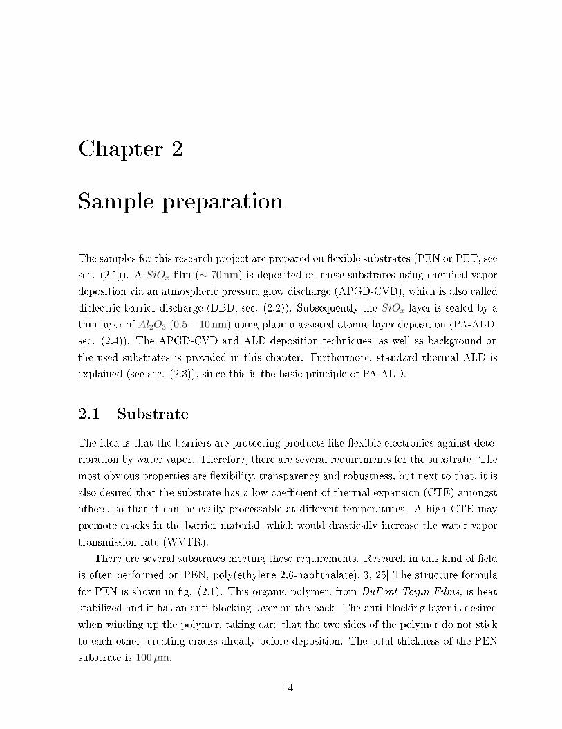
Figure 2.4: Roll-to-roll setup of APGD-CVD. On the left side the polymer substrate isunwinded, while on the right it is winded up again. Also the gas injection system is shownon the left.
The accumulation of negative ions leads to the formation of dust, increasing the pinhole
density in the �lm.[32]
The setup can also be seen in �g. (2.4). This �gure shows two identical webs in between
the electrodes. Both webs work as a dielectric, reducing the conduction current between
the electrodes so that the probability of an arc discharge is reduced. Furthermore, it can
be seen that this is a roll-to-roll setup. On the left the two coils are unwinding, while the
coils on the right are winding up the foil. However, to prevent the samples from winding
induced damage, the samples are cut from the web before any mechanical contact.
The plasma itself is generated between the electrodes by a glow discharge. The elec-
trodes are placed ±0.5 mm from each other so that a gas mixture can �ow in between the
electrodes. That gas is injected by a gas injection system, which is placed just on the left
of these electrodes.
As mentioned in the introduction, the idea is to deposit a SiOx layer with a high
deposition rate (HDR). The resulting SiOx layer is a percolated layer (columnar structures
of interconnecting defects) with a relatively high WVTR, but which can be sealed by
atomic layer deposition (ALD). The gas �ows for this type of layer are set at: 15 slm of
N2, 1.0 slm of Ar, 1.8 slm of O2 and 5.5 g/hr of TEOS. TEOS (tetra-ethyl orthosilicate) is
the precursor, reacting with the oxygen, so that SiOx is deposited. Under these conditions,
17
the thickness of the deposited layers is approximately 70 nm. The growth speed for this
HDR SiOx is:
vgrowth(
HDR SiOx
)= 24.6 nm/s (2.1)
On the other hand (as shown in �g. (1.4), together with the previously explained HDR
deposited SiOx), is it also possible to deposit a low deposition rate SiOx barrier. When
using the correct parameters, a much better barrier can be deposited, but - as said - this
is deposited much slower, resulting in a growth speed as shown in eq. (2.2). Furthermore,
this barrier does not have such an improvement when depositing an ALD layer on top of
it. This will be extensively discussed in sect. (4.3). This LDR barrier is deposited using
gas �ows of 15 slm of N2, 1.0 slm of Ar, 1.0 slm of O2 and just 1.0 g/hr of TEOS. The power
will here be 600 W, while for the HDR barrier, it will be 650 W.
vgrowth(
LDR SiOx
)= 4.90 nm/s (2.2)
Especially the oxygen in the mixtures is important for the plasma chemistry. Of course
for depositing the silicon oxide, promoting the precursor decomposition, but also in the
carbon content of the �lm. For low oxygen concentration, lots of carbon can be found (up
to 60 %), while for higher oxygen concentrations, the carbon content can be reduced to ±
5 %.[32]
Furthermore, to get a better idea of the discharge deposition process, the plasma is
simulated using BOLSIG+. This program is used to determine transport coe�cients and
rate coe�cients, which are calculated from collision cross sections. The exact formulas
used to do this are shown in Hagelaar and Pitchford[11]. It should be mentioned that
this is more like a rough estimation in order to get some idea of the plasma properties.
The determination of the exact properties is behind the scope of this research, which is
more focused on the properties of the deposited �lms, than that it really focuses on the
techniques that are used.
As mentioned, the cross sections for momentum transfer (�elastic� or �momentum�, see
[11]), excitation, ionization and detachment are imported into the BOLSIG+ simulation
program. The cross sections of gasses which are used - Ar, N2 and O2 - are already in the
database of the program. Only the cross sections of TEOS should be added. These are
determined by Morgen et al.[22] and they are shown in �g. (2.5). The ionization cross
sections of the four materials are also shown in �g. (2.6).
In order to correctly simulate the plasma, some parameters should be determined. At
18

Figure 2.5: TEOS cross sections by Morgan et al.[22] These are the cross sections forelastic momentum transfer (Qe), inelastic momentum transfer (Qm), excitation (Qv, fortwo di�erent excitation energies), ionization (Qi) and detachment (Qd).
Figure 2.6: Ionization cross sections (m2) of all four materials in the gas mixture, whichare ionized by the glow discharge, as a function of energy (eV).
19
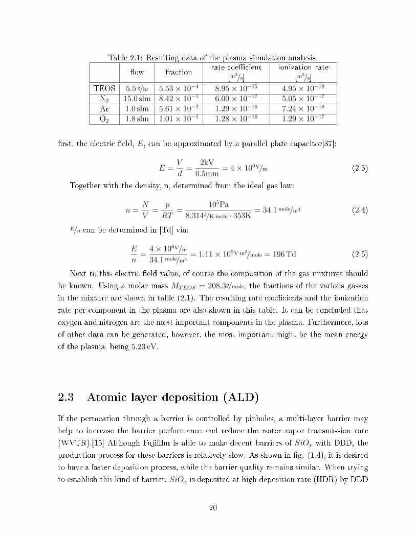
Table 2.1: Resulting data of the plasma simulation analysis.
�ow fractionrate coe�cient
[m3/s]ionization rate
[m3/s]
TEOS 5.5 g/hr 5.53× 10⁻⁴ 8.95× 10⁻¹⁵ 4.95× 10⁻¹⁸
N2 15.0 slm 8.42× 10⁻¹ 6.00× 10⁻¹⁷ 5.05× 10⁻¹⁷
Ar 1.0 slm 5.61× 10⁻² 1.29× 10⁻¹⁶ 7.24× 10⁻¹⁸
O2 1.8 slm 1.01× 10⁻¹ 1.28× 10⁻¹⁶ 1.29× 10⁻¹⁷
�rst, the electric �eld, E, can be approximated by a parallel plate capacitor[37]:
E =V
d=
2kV
0.5mm= 4× 10⁶V/m (2.3)
Together with the density, n, determined from the ideal gas law:
n =N
V=
p
RT=
105Pa
8.314J/K·mole · 353K= 34.1 mole/m3 (2.4)
E/n can be determined in [Td] via:
E
n=
4× 10⁶V/m
34.1 mole/m3= 1.11× 10⁵V·m2/mole = 196 Td (2.5)
Next to this electric �eld value, of course the composition of the gas mixtures should
be known. Using a molar mass MTEOS = 208.3g/mole, the fractions of the various gasses
in the mixture are shown in table (2.1). The resulting rate coe�cients and the ionization
rate per component in the plasma are also shown in this table. It can be concluded that
oxygen and nitrogen are the most important components in the plasma. Furthermore, lots
of other data can be generated, however, the most important might be the mean energy
of the plasma, being 5.23 eV.
2.3 Atomic layer deposition (ALD)
If the permeation through a barrier is controlled by pinholes, a multi-layer barrier may
help to increase the barrier performance and reduce the water vapor transmission rate
(WVTR).[15] Although Fuji�lm is able to make decent barriers of SiOx with DBD, the
production process for these barriers is relatively slow. As shown in �g. (1.4), it is desired
to have a faster deposition process, while the barrier quality remains similar. When trying
to establish this kind of barrier, SiOx is deposited at high deposition rate (HDR) by DBD
20
and covered by a very thin layer (0.5−10 nm) of Al2O3. The deposition of the Al2O3 layer
can be performed by atomic layer deposition (ALD). This can also be deposited relatively
fast - because the Al2O3 layer is very thin - so that the total production process can
be performed fast enough and the production of barrier layers becomes feasible both in
production time and in costs. In this section the basic principle of ALD will be explained,
while in the next section, remarks are made about the di�erences between plasma assisted
ALD (PA-ALD) - the deposition method which is used in this research project - and
standard thermal ALD, as well as that the speci�c conditions and deposition parameters
are explained.
The basic principle of the most common form of ALD - thermal ALD - is a deposition
process which consist of four steps, which are consistently performed when the previous
step is �nished.[9] In the �rst of these steps, the surface is exposed to an aluminum
depositing precursor, being trimethylaluminum (TMA, Al(CH3)3). Second, the ALD
deposition chamber is cleaned from previously used gasses by �ushing it with a non-
reactive gas. This is called purging and in this case, argon is used for this. The purging
step should be included, because TMA and the second precursor, H2O, are heavily reactive
when brought together. After this purging step, the second precursor - water vapor - is
lead into the chamber. This is an oxidizing precursor, depositing oxygen atoms on the
surface, so that the desired AlOx layer is created, as well as it prepares the surface for a
new dose of TMA. At last, the chamber is again purged with argon, after which the next
cycle can start by TMA exposure again.
The actual Al2O3 �lm is grown in the second and fourth step of the ALD cycle by
exposing the surface to the precursors, TMA and H2O. The precursors react with speci�c
surface groups (−OH groups and −CH3 groups respectively) so that TMA deposits alu-
minum on the surface and the water vapor deposits oxygen, leaving speci�c surface groups
behind again for the next step to take place. The actual chemical surface reactions of this
deposition process are shown in eq. (2.6) and (2.7). The molecules which are attached to
the surface are marked with an (*)[9]:
AlOH*+Al(CH3)3 →AlOAl(CH3)2*+CH4 (2.6)
AlCH3*+H2O→AlOH*+CH4 (2.7)
The reactions are graphically shown in �g. (2.7). In the �rst half of the ALD cycle
(eq. (2.6)), the TMA adsorbs at a hydroxide group at the surface, after which CH4
is formed from the hydrogen atom at the surface and one of the methyl groups of the
21

TMA. Immediately after the formation of this CH4 group, the CH4 is reabsorbed from
the surface, leaving aluminum at the surface, together with two methyl groups. So in the
�rst half of the ALD cycle, the hydrogen atom at the surface is replaced by aluminum,
carrying two −CH3 groups. This is also shown in the second (middle) illustration in �g.
(2.7).
For the second growing step, after purging the reactor with Ar, the surface is exposed
to water vapor. The water adsorbs at the Al atom at the surface. Then again CH4 is
formed from one hydrogen atom of the water molecule and a methyl group, which was
deposited at the surface during the �rst step. Almost immediately after formation, the
CH4 is again desorbed from the surface, leaving a hydroxide group at the surface. In this
way an oxygen atom is deposited at the surface, while the surface is ready to interact with
TMA again.[35] This is also shown in bottom part of �g. (2.7).
In principle, when performing both half-cycles together, each containing one of the
deposition steps and a purging step, a full mono-layer of Al2O3 can be deposited. Although
it is shown that it takes more than one cycle to deposit a complete mono-layer (explained
later on in this section), a general equation can be derived for the thermal Al2O3 ALD by
correctly adding up eq. (2.6) and eq. (2.7):
2Al(CH3)3 + 3H2O → Al2O3 + 6CH4 (2.8)
On the left hand side of this equation, both precursors are present: TMA and water,
while on the right the exhausted methane shows up, together with the aluminum oxide,
which is deposited on the surface. This can also be concluded from �g. (2.7). On the
left site of this �gure, the precursors and the exhausted methane are also shown, together
with the amounts of all these substances. The deposited Al2O3 is of course shown in the
layer itself (on the right side of the �gure).
This kind of thermal Al2O3 ALD can be performed because of the high binding energy
of the Al −O bond.[9] Forming this bond brings the system in a lower, preferable energy
state, since it is exothermic. Therefore during the �rst step (eq. (2.6)), the aluminum atom
of the TMA prefers sticking to the surface oxide, causing the formation and desorption of
a CH4 molecule. The same holds for the second step (eq. (2.7)), where the oxygen atom
prefers creating a Al −O bond, which again results in the desorption of a CH4 molecule.
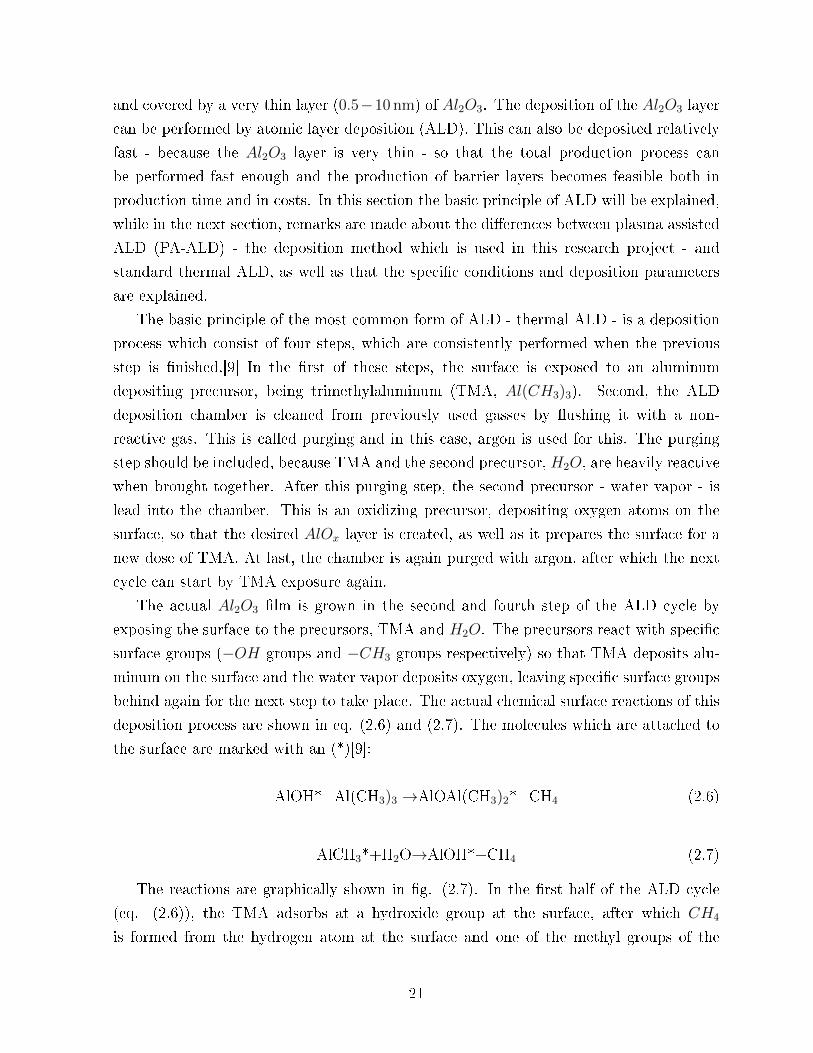
Fig. (2.8) shows the di�erence in energy between the various steps of the ALD process. On
the left side the various energies of the �rst step are shown (the adsorption of TMA), while
on the right side the speci�c energies of the reaction of the changed surface with water are
shown. In the latter, the normal numbers are the reactions of Al(OH)2−CH3 with H2O,
while the numbers in parentheses are the values of the reactions of Al(OH)(CH3)−CH3
22

Figure 2.7: Principle of thermal Al2O3 ALD using TMA and H2O as (metal- and oxide-) precursors. The upper �gure (on the right) shows a −OH terminated surface at thebeginning of an ALD cycle. After purging with Ar, the �rst precursor (TMA) is lead intothe reactor. The TMA adsorbs at the O surface atom via the Al atom. Immediatelyafter that, a CH4 molecule is formed and desorbed from the surface. The Al atom withthe two remaining CH3 groups takes the place of the H atom, as shown in the middle�gure. Now the reactor is again purged with Ar to remove the released methane andthe remaining TMA. Then water vapor is lead into the reaction chamber, so that −OHgroups can replace the methyl groups, while producing CH4 again. The resulting surfaceis shown in the bottom �gure (on the right); it is the same, with the di�erence that anextra layer of Al2O3 was deposited on the surface.
23
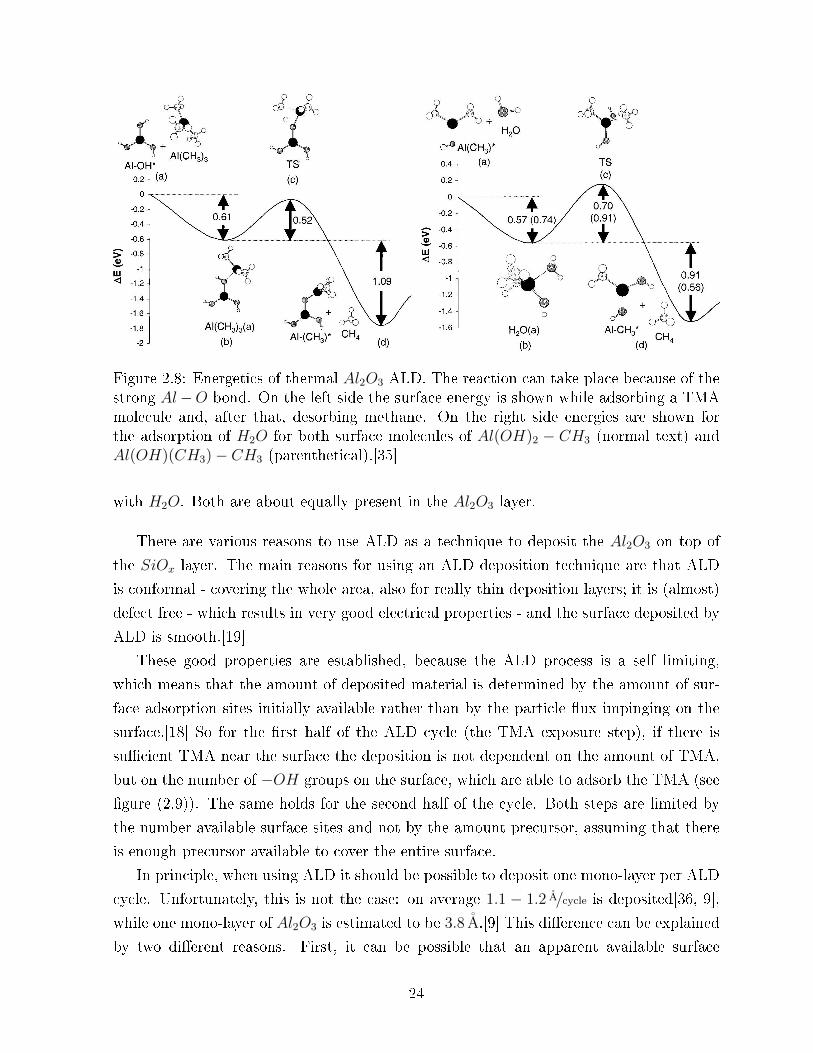
Figure 2.8: Energetics of thermal Al2O3 ALD. The reaction can take place because of thestrong Al−O bond. On the left side the surface energy is shown while adsorbing a TMAmolecule and, after that, desorbing methane. On the right side energies are shown forthe adsorption of H2O for both surface molecules of Al(OH)2 − CH3 (normal text) andAl(OH)(CH3)− CH3 (parenthetical).[35]
with H2O. Both are about equally present in the Al2O3 layer.
There are various reasons to use ALD as a technique to deposit the Al2O3 on top of
the SiOx layer. The main reasons for using an ALD deposition technique are that ALD
is conformal - covering the whole area, also for really thin deposition layers; it is (almost)
defect free - which results in very good electrical properties - and the surface deposited by
ALD is smooth.[19]
These good properties are established, because the ALD process is a self limiting,
which means that the amount of deposited material is determined by the amount of sur-
face adsorption sites initially available rather than by the particle �ux impinging on the
surface.[18] So for the �rst half of the ALD cycle (the TMA exposure step), if there is
su�cient TMA near the surface the deposition is not dependent on the amount of TMA,
but on the number of −OH groups on the surface, which are able to adsorb the TMA (see
�gure (2.9)). The same holds for the second half of the cycle. Both steps are limited by
the number available surface sites and not by the amount precursor, assuming that there
is enough precursor available to cover the entire surface.
In principle, when using ALD it should be possible to deposit one mono-layer per ALD
cycle. Unfortunately, this is not the case: on average 1.1 − 1.2 A/cycle is deposited[36, 9],
while one mono-layer of Al2O3 is estimated to be 3.8 A.[9] This di�erence can be explained
by two di�erent reasons. First, it can be possible that an apparent available surface
24

Figure 2.9: In this �gure, it can be seen that if enough TMA is available near the surface,the growth per cycle is constant.[14]
site is not available. An example of this is steric repulsion; if there is a TMA molecule
adsorbed at a surface site, it can be di�cult for the adjacent surface site to also adsorb
a TMA molecule. The methyl groups which are left at the surface are then screening the
available surface site. Problems with the removal of the reaction byproducts (methane)
can also counteract adsorption at all available surface surface sites. The second problem
limiting the growth is the desorption of adsorbed precursor material. Especially for higher
temperatures (e.g. 300 ºC) an adsorbed molecule can again be desorbed due the high
available thermal energy.[35] Together with problems like decomposition or condensation
of the precursor or incomplete reactions due to the lack of energy, these problems are shown
in �g. (2.10). This �gure also shows that there is only a relatively small temperature
window for which ALD is possible.
2.4 Plasma assisted ALD
As mentioned before, not standard thermal ALD is used, but plasma assisted ALD. Al-
though plasma assisted ALD (PA-ALD) and thermal ALD are quite similar, PA-ALD
has some advantages over thermal ALD. The main advantage is that PA-ALD can be
performed at much lower temperatures; even at room temperature. This is of course
interesting from a production kind of view.
The main di�erence is the use of an oxygen plasma, instead of water vapor, as an
oxidizing precursor. Due to the use of this plasma, reaction mechanisms also change. The
25
Figure 2.10: ALD window. There is a limited range op temperatures at which ALD canbe performed.[9]
�rst half of the ALD cycle (eq. (2.6)) remains the same - using TMA as a precursor and
only exhausting CH4 - but the second part becomes a more combustion type of reaction.
That reaction, however, is not as clearly de�ned as with thermal ALD. The combustion
of the −CH3 groups should result in combustion products, like CO2 and H2O, but due
to the presence the oxygen plasma, CO2 can be decomposed, resulting in CO.[12] The
decomposition possibilities are also shown in the equations below[14]:
e+ CO2 → e+ CO +O (2.9)
e+H2O → e+H +OH (2.10)
Due to these reactions, various reaction products are found. This is also shown in
�g. (2.11): As mentioned before H2O and CO2 will be found during the plasma exposure
step in the ALD cycle, but also CO (due to decomposition of CO2), OH (immediately
adsorbed at the surface, but formed due to decomposition of H2O) and CxHy (formed
out of the reaction of some −CH3 groups (desorbed from the surface due to the presence
of the oxygen plasma) and H (left from the decomposition of H2O)) are detected when
analyzing the various gasses.[12]
The precursors for these reactions can be brought into the deposition chamber of the
Oxford Instruments FlexAl in two ways. After pumping the chamber down to a pressure
of 10−6 bar, the �rst option is to simply lead the precursors directly into the chamber, so
that the reactions can take place. If the one of the reactions is �nished, the remaining
precursor, as well as the reaction products should be pumped o� and the reaction chamber
should be purged. In order to clean the reaction chamber well enough, purging should
26

Figure 2.11: Reaction products after plasma exposure in PA-ALD.[14]
Figure 2.12: Scheme representing the timing of the various gas �ows in the ALD cycle. Itis also shown when power is applied to the RF coil, ionizing the oxygen, so that a plasmais created.
be done for a relatively long time. Therefore the second option is to use a noble, non
reactive, carrier gas (Ar) to lead the precursor to the reaction chamber. In this way, the
ALD reaction remains the same, but purging times can be decreased. In �g. (2.12) a
timing scheme is shown of which gasses are lead into the reaction chamber. The gasses
are continuously pumped o�. This can be seen in �g. (2.13), which shows the reaction
chamber setup. The TMA is lead into the reaction chamber from the side, while the
oxygen is lead into the chamber from above, passing a radio frequent coil (RF), which can
ionize the oxygen to enhance the oxidation step in the ALD cycle. This setup is called a
remote plasma, meaning that the plasma is created further above the sample surface, but
there is a small, low energy, particle �ux going to the surface.[16]
At last, of course the growth speed for this setup is important, since the project is
focusing on the increase of the deposition speed in order to improve the feasibility of the
production of barrier layers. ALD is, however, a relatively slow process, but because of
27

Figure 2.13: Setup of the ALD reaction chamber.
its properties only a very thin layer of Al2O3 is needed. Using the cycle as shown in �g.
(2.12) a growth speed can be determined, in order to compare ALD with deposition by
DBD. This is of course important for the production of these barriers.
vgrowth = 0.029 nm/s (2.11)
It can be concluded that using this setup, thin �lms of Al2O3 can be deposited, sealing
the SiOx layer. PA-ALD is chosen to be the method to deposit the �lms. It is preferred to
use PA-ALD instead of thermal ALD, because the �lms can be deposited at lower temper-
atures, while remaining high �lm quality, such as conformality and a low defect density.[9]
Furthermore, growth rates are higher and the purging steps can be shortened[12], resulting
in a decreased deposition time, attractive for industrial production.
28

�
29
Chapter 3
Analysis methods
3.1 Water vapor transmission rate (WVTR)
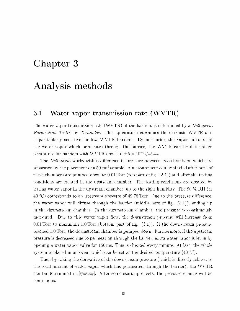
The water vapor transmission rate (WVTR) of the barriers is determined by a Deltaperm
Permeation Tester by Technolox. This apparatus determines the extrinsic WVTR and
is particularly sensitive for low WVTR barriers. By measuring the vapor pressure of
the water vapor which permeates through the barrier, the WVTR can be determined
accurately for barriers with WVTR down to ±5× 10⁻⁴g/m2·day.
The Deltaperm works with a di�erence in pressure between two chambers, which are
separated by the placement of a 50 cm2 sample. A measurement can be started after both of
these chambers are pumped down to 0.01 Torr (top part of �g. (3.1)) and after the testing
conditions are created in the upstream chamber. The testing conditions are created by
letting water vapor in the upstream chamber, up to the right humidity. The 90 % RH (at
40 ºC) corresponds to an upstream pressure of 49.78 Torr. Due to the pressure di�erence,
the water vapor will di�use through the barrier (middle part of �g. (3.1)), ending up
in the downstream chamber. In the downstream chamber, the pressure is continuously
measured. Due to this water vapor �ow, the downstream pressure will increase from
0.01 Torr to maximum 1.0 Torr (bottom part of �g. (3.1)). If the downstream pressure
reached 1.0 Torr, the downstream chamber is pumped down. Furthermore, if the upstream
pressure is decreased due to permeation through the barrier, extra water vapor is let in by
opening a water vapor valve for 150 ms. This is checked every minute. At last, the whole
system is placed in an oven, which can be set at the desired temperature (40 ºC).
Then by taking the derivative of the downstream pressure (which is directly related to
the total amount of water vapor which has permeated through the barrier), the WVTR
can be determined in [g/m2·day]. After some start-up e�ects, the pressure change will be
continuous.
30

Figure 3.1: The working of the Deltaperm.[23]
The barriers should be used at atmospheric conditions (e.g. 20 ºC and 50 % relative
humidity (RH)). Experiments, however, are often performed at other conditions in tem-
perature and relative humidity, e.g. 38 ºC / 85 % RH[4], 20 ºC / 50 % RH[13, 15] or 23 ºC
/ 100 % RH[5]. Also our experiments are not performed at atmospheric conditions, but
at 40 ºC and 90 % RH. When using tougher conditions, measurements can be performed
faster, because the permeation is higher. That is because the permeation (P) depends on
both the solubility (S) of water vapor into the barrier and the di�usion (D) through the
barrier.[27] This is shown in �g. (3.2) and in eq. (3.1).
P = S ×D (3.1)
At last, it should be mentioned that there are some measurements performed on 100µm
aluminum foil. Since this foil can be assumed to be a very good barrier for the water
vapor, this can be used to determine the minimum detection limit of this apparatus. This
minimum detection limit may be controlled by (air) leakage between the two chamber
or via the inlet of water vapor from the outside into the downstream chamber. This
can permeate via the grease and rubber, which are used to place the sample properly.
The average of these measurements (�ve measurements are performed) is (3.6 ± 0.5) ×
31
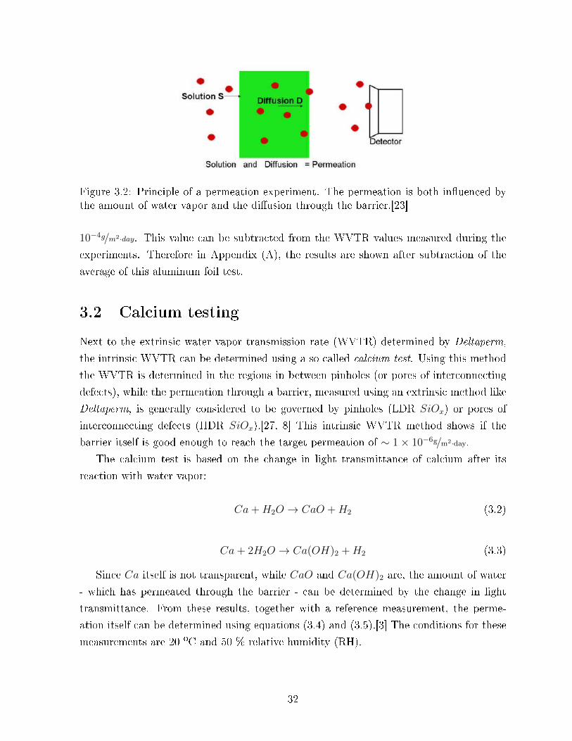
Figure 3.2: Principle of a permeation experiment. The permeation is both in�uenced bythe amount of water vapor and the di�usion through the barrier.[23]
10−4g/m2·day. This value can be subtracted from the WVTR values measured during the
experiments. Therefore in Appendix (A), the results are shown after subtraction of the
average of this aluminum foil test.
3.2 Calcium testing
Next to the extrinsic water vapor transmission rate (WVTR) determined by Deltaperm,
the intrinsic WVTR can be determined using a so called calcium test. Using this method
the WVTR is determined in the regions in between pinholes (or pores of interconnecting
defects), while the permeation through a barrier, measured using an extrinsic method like
Deltaperm, is generally considered to be governed by pinholes (LDR SiOx) or pores of
interconnecting defects (HDR SiOx).[27, 8] This intrinsic WVTR method shows if the
barrier itself is good enough to reach the target permeation of ∼ 1× 10⁻⁶g/m2·day.
The calcium test is based on the change in light transmittance of calcium after its
reaction with water vapor:
Ca+H2O → CaO +H2 (3.2)
Ca+ 2H2O → Ca(OH)2 +H2 (3.3)
Since Ca itself is not transparent, while CaO and Ca(OH)2 are, the amount of water
- which has permeated through the barrier - can be determined by the change in light
transmittance. From these results, together with a reference measurement, the perme-
ation itself can be determined using equations (3.4) and (3.5).[3] The conditions for these
measurements are 20 ºC and 50 % relative humidity (RH).
32

Figure 3.3: The various layers in a Ca test. The substrate, together with the barrier iscovered by several small squares of Ca. The whole is encapsulated by SiNx : H so thatpermeation of water vapor only goes via the barrier. Due to the permeation of water vaporthrough the barrier, the Ca becomes transparent, because of the oxidation to CaO andCa(OH)2.
WV TR =ρ (CaO)D (CaO)
t× m (H2O)
m (CaO)(3.4)
WV TR =ρ (Ca (OH)2)D (Ca (OH)2)
t× 2m (H2O)
m (Ca (OH)2)(3.5)
It is shown that it is both possible to form CaO and Ca(OH)2 (eq. (3.2) and (3.3)).
Therefore the WVTR can also has to be determined for both of these (eq. (3.4) and (3.5))
and they should be used in their correct ratio. However, when working out eq. (3.4)
and (3.5), it can be determined that for the same change in light transmittance, D, the
di�erence between these two options is less than 3 %.[3]
For this kind of WVTR determination, 40 nm of Ca is deposited by thermal evaporation
on top of the barrier. The Ca is prepared in two arrays of 3×3 squares of Ca, each with a
size of ∼ 5× 5mm. The Ca is encapsulated by a 300 nm thick layer of PE-CVD deposited
SiNx : H. According to Philips, the SiNx : H layer has a barrier of ∼ 10−7, so that the
change in transmittance is mainly due to permeation through our barrier. This is also
shown in �g. (3.3). The setup is calibrated by measuring the [Ca]/[O] ratio by Rutherford
backscattering (RBS) and the transparency at the same time.
3.3 Interferometry
Another technique which is used to analyze the samples is interferometry. A Veeco Wyko
NT9100 is used as an optical pro�ler, which is able to determine surface height with an
33

Figure 3.4: Resulting �gure of an interferometry scan. At each position the height of thesurface is determined.
accuracy of ∼ 1 A. When analyzing the surface structure, the surface roughness and the
number of defects can be determined. This is done using a beam splitter, which splits
a laser beam, sending half of the signal to the sample, while the other half is send to a
mirror. Depending on the phase di�erence between both re�ected waves, the distance to
the surface can be determined. This can be done very accurately. From these results a
surface height pro�le can be obtained. To correct for surface tilting and curving of the
substrate an algorithm to �lter the low spatial frequencies was applied. This algorithm is
available in the software package. Results are shown in �g. (3.4). The colors indicate the
surface height as shown in the index.
In this project interferometry is used to determine the surface roughness and the num-
ber of surface defects of the various possible substrates and deposited samples. In order to
determine the surface roughness, a scan of the surface is done using a magni�cation of 100x.
The �eld of view is 47× 63µm, which is digitized with a resolution of (480× 640 pixels).
From the results of the surface height at each spot a 2D plot can be determined, using
colors indicating the surface height. An example of such a �gure is shown in �g. (3.4).
Such a �gure can, therefore, be used to determine the surface roughness. In fact, there are
various numbers related to surface roughness. The most general one, which is applicable
here, is the Ra value. To determine Ra, �rst the average surface height, z, is determined
(see eq. (3.6)). Then the absolute deviation from this average is determined for each
point; this is averaged again (see eq. (3.7)).
34

z =1
A
¨zdA (3.6)
Ra =1
A
¨|z − z| dA (3.7)
Furthermore, the number of defects can be determined using interferometry. This is
important since defects can lead to pinholes, which largely decrease the performance of
the barrier layer. Pinholes, originating from the connection of defects and pores, increase
the WVTR enormously by allowing water vapor to �ow unhindered through a path of
interconnecting defects and pores in the barrier. The defect analysis is done by the de-
termination spots with a certain area, which stand out of the (average) surface a certain
height. The last one is the threshold value and is varied, while the area has been kept
constant. The threshold value can be seen as a measure for the size of the defect, while
the area, is just for excluding very small features and measurement errors (spikes). So
for example, an area of 25 × 25 nm should completely stand out of the surface for 5 nm.
The number of defects (or other features) can be set out in a graph as a function of the
threshold value, in order to compare various surfaces. A single measurement is done using
a magni�cation of 40x over an area of 1.84× 10⁻² mm2, while 12 measurements are done
per sample.
At last, there is also a special method from Fuji�lm to determine the number of pin-
holes. In this method, the pinholes in the barrier layer can be visualized and can be
detected by interferometry. Using a magni�cation of 5x, an area is scanned of 5× 5 mm.
Per sample, �ve measurements were done at �ve di�erent spots. Statistical analysis can
be done on these measurements to determine properties of these pinholes, however, the
most important property is the average number of pinholes per cm2.
3.4 Spectroscopic Ellipsometry (SE)
The thickness of the various layers of the samples is determined using spectroscopic ellip-
sometry (SE). Using this technique, the thickness of the SiOx and the Al2O3 layers can
be determined, as well as possibly present intermix layers due to the possible penetra-
tion of Al2O3 into the SiOx. These measurements are performed using a Woollam M2000
Multi-Angle Ellipsometer.
The principle of SE is shown in �g. (3.5). A linearly polarized light beam is send to the
sample. The polarization of the light is changed as a function of the wavelength due to the
35

Figure 3.5: The basic principle of SE.[28]
electrical and structural properties of the sample layers. The change in the polarization can
be depicted using psi (Y) and delta (D). These are the variables measured as a function of
the wavelength of the light. These can be converted to the complex re�ection coe�cients
rp and rs, parallel (p) and perpendicular (s) to the plane of incidence, via
ρ ≡ tan Ψ exp (i∆) ≡ rprs≡
Erp/Eip
Ers/Eis
(3.8)
An optical model should be used to �t the results found for Ψ and ∆. All refractive
indexes and absorption coe�cients come together in ρ:
tan Ψ exp (i∆) = ρ (N0, N1, N2, d, θ0) (3.9)
In this equation, only the refractive indexes and absorption coe�cients of a model with
a single thin �lm on a substrate are included, as shown in �g. (3.6) (left). The model
which is used in our research is also shown in (3.6) (right). In �g. (3.6) it can also be
seen that the barrier consists of several layers. The model consists of the PEN substrate
(∼ 100µm), together with the SiOx and Al2O3 barrier layers. At the backside, there is a
thin anti-blocking layer (sect. (2.1)), however, to make sure that there is back re�ection,
the backside is scratched. Most of this anti-blocking layer is also remove by this.
At last, it should also be mentioned that the samples are anisotropic. Therefore it
depends in which direction of the sample, the measurements are performed. As is shown
by Roelofs[28] the refractive index of PEN is larger in web roll direction, than in the
direction perpendicular to that. It can be assumed that this di�erence in refractive index
is caused by the tension on the web during the (un-)winding process. Because of the
anisotropy it is important that each time a SE measurement is performed, the sample
is oriented the same way. It is standard that the measurements are performed in the
direction perpendicular to the web roll direction.
36

Figure 3.6: On the left a basic illustration of SE is shown. The incoming light ray isre�ected at the various interfaces, where the refractive index changes. Also part of thelight is transmitted. On the right the SE model for the deposited barriers is shown,containing the substrate (PEN, together with an anti-blocking layer on the backside) andlayers of SiOx and Al2O3. The backside of the samples is scratched, so that only re�ectionof the deposited layers is seen.
37

Chapter 4
Results & Discussion
In this chapter the experimental results are presented and discussed. The results are
discussed starting with the available substrates (sect. (4.1)), followed by single layer
barriers (sect. (4.2)) and subsequently the sealing of HDR SiOx with a thin layer of
Al2O3, both with a standard ALD process (sect. (4.3)) and a longer oxygen plasma
exposure time in the ALD cycle (sect. (4.4)). The last section of this chapter (sect. (4.5))
is dedicated to the determination of the activation energy of the barrier layers prepared
in sect. (4.4).
For each section individually, the results are discussed and explanations for the various
phenomena are proposed after the presentation of the bare results. The explanations are
supported by literature. Everything is brought together in a �nal conclusion in chapter 5.
4.1 Surface analysis of substrates
It is explained in sect. (2.1) that for this project four di�erent substrates are available.
Because of the various requirements of the substrates - like transmittance of visible light,
mechanical �exibility, thermal stability, smoothness of the surface and of course that it
should relatively cheap - there are just a few possible substrates, mainly polymers. PEN
(polyethylene naphthalate) and PET (polyethylene terephthalate) are examples of sub-
strates which meet the requirements. Both substrates can also be provided with a pla-
narizing �lm to make the surface even smoother, this is called a TP-layer. Both PEN and
PET, as well as their potential TP-layer are already more extensively described in sect.
(2.1). Two characteristics of the di�erent possible substrates are investigated using inter-
ferometry. In order to compare PEN, PEN/TP, PET and PET/TP the surface roughness
and the number of surface defects are determined using interferometry. The speci�cations
in determining these properties are stepwise explained in sect. (3.3).
38
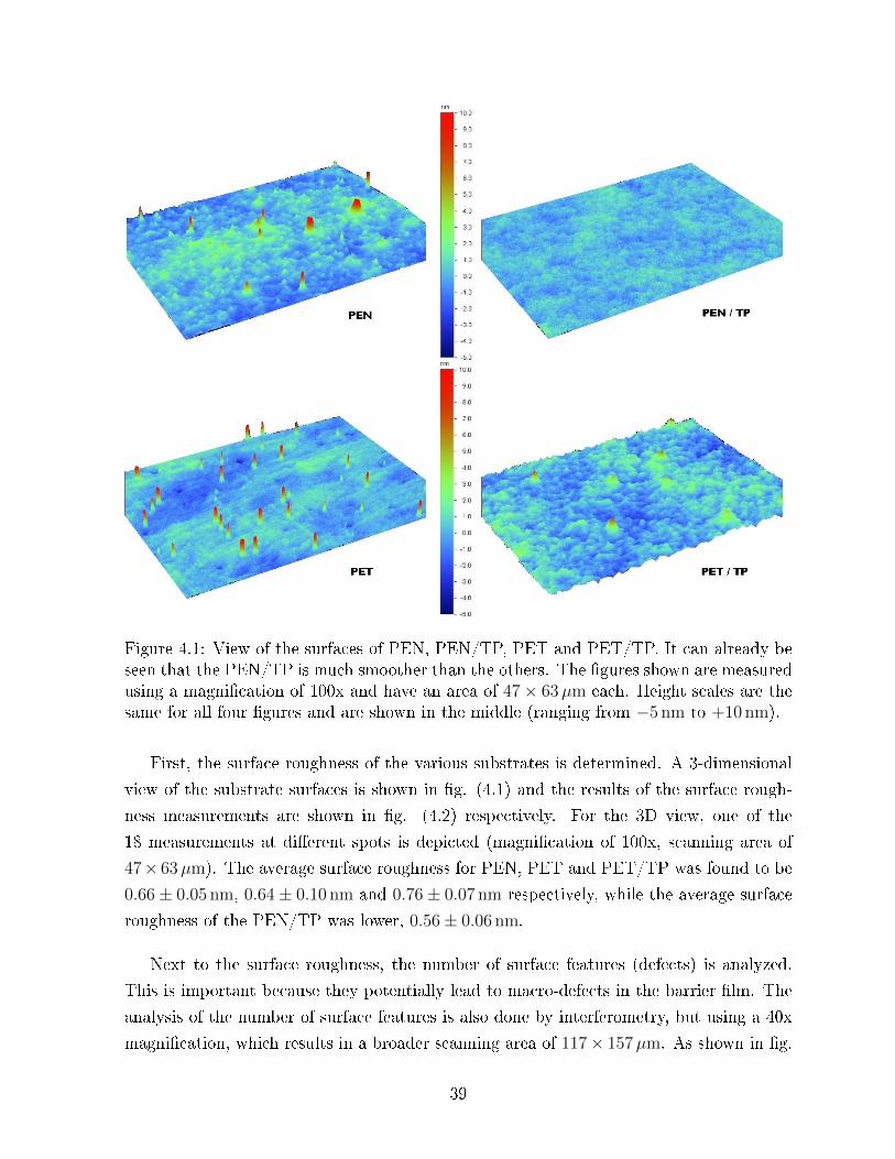
Figure 4.1: View of the surfaces of PEN, PEN/TP, PET and PET/TP. It can already beseen that the PEN/TP is much smoother than the others. The �gures shown are measuredusing a magni�cation of 100x and have an area of 47× 63µm each. Height scales are thesame for all four �gures and are shown in the middle (ranging from −5 nm to +10 nm).
First, the surface roughness of the various substrates is determined. A 3-dimensional
view of the substrate surfaces is shown in �g. (4.1) and the results of the surface rough-
ness measurements are shown in �g. (4.2) respectively. For the 3D view, one of the
18 measurements at di�erent spots is depicted (magni�cation of 100x, scanning area of
47× 63µm). The average surface roughness for PEN, PET and PET/TP was found to be
0.66± 0.05 nm, 0.64± 0.10 nm and 0.76± 0.07 nm respectively, while the average surface
roughness of the PEN/TP was lower, 0.56± 0.06 nm.
Next to the surface roughness, the number of surface features (defects) is analyzed.
This is important because they potentially lead to macro-defects in the barrier �lm. The
analysis of the number of surface features is also done by interferometry, but using a 40x
magni�cation, which results in a broader scanning area of 117× 157µm. As shown in �g.
39

Figure 4.2: Results of the surface roughness analysis of the di�erent substrates. Thesurface roughness of PEN/TP is signi�cantly lower than the roughness of the other sub-strates. The data are averaged over 18 measurements at di�erent spots (magni�cation of100x, scanning area of 47× 63µm).
(4.1) the surface contains several features, which are considered to be a result of defects
near the surface. The number of features can be determined using a minimum spot size
and a threshold value. First the average surface height is determined, which is corrected
for the fact that the surface (and the stage) is tilted and that the surface might be bend.
Then, only the larger features are taken into account, using a threshold value for the height
of the defect. This value is varied in order to determine the size (especially the height) of
the defects. At last, the features should have an area of nine pixels (625 nm2) being higher
than the threshold value. This is to ensure that no measurement errors intermix with the
feature counting. This is a relatively large area, also due to the low lateral resolution of
interferometer (∼ 1× 1µm) compared to the height resolution (up to ∼ 1 A). Due to this
low lateral resolution it might be possible that large thin features (spikes) are spread out
to broader features with a much smaller peak height. Therefore, the size of the features
might be a bit of an under estimate, depending structure of the features near the surface.
Using this procedure, the number of defects on the surface is determined, as well as
an estimation is given for the size of these defects via the threshold value. This is shown
in �g. (4.3). It can be seen that independent of the threshold value, there are less defects
on the PEN/TP substrate than on the other substrates. Finally, it should be mentioned
that, although the density of features is large, the total measured area is relatively small.
Therefore the total number of measured features for threshold values higher than 7−15 nm
40

Figure 4.3: Analysis of the number of surface defects. It is shown that the number ofsurface defects is much lower for the PEN/TP than for the other substrates: bare PEN,PET/TP and bare PET. The data are averaged over 12 measurements, with each an areaof 1.84× 10⁻²mm2.
is, depending on which substrate is analyzed, actually zero.
From �g. (4.1), (4.2) and (4.3) it can be concluded that the surface roughness of the
PEN/TP surface is lower than the surface roughness of the others (Ra = 0.56 nm compared
to 0.66, 0.64 or 0.76 nm for PEN, PET and PET/TP respectively), as well as that
there are less defects found on the PEN/TP substrate. Although there are much more
requirements on the substrate - like �exibility and a low coe�cient of thermal expansion
- at least from these results, PEN/TP looks favorable as a substrate material, because a
smooth substrate with few, small defects, leads to smoothly deposited barrier layers, with
less defects and a lower water vapor permeation, which is better for protecting �exible
organic electronics for oxidation.[4] However, it should be mentioned that the porosity of
the substrate also plays a role in the barrier performance.[36] This will be discussed in
sect. 4.2.
Furthermore it is interesting to see that for PET (0.64± 0.10 nm), the substrate itself
is smoother than that of PET/TP (0.76±0.07 nm), while the TP-layer should increase the
smoothness of the substrate. This can be explained by the overview of the substrate in �g.
(4.1); it can be seen that PET/TP has a bit of a bumpy surface structure, while bare PET
has some big features. Because the surface roughness is determined by the deviation from
the average surface height (eq. (3.6) and eq. (3.7)), the PET/TP has lots of contributions
41

from the bumpy structure, while PET only has a few from its spike-like features. The
measured surface roughness of PET can therefore be lower than that of PET/TP, but
the working as a substrate for depositing a barrier might be better for PET/TP, because
smooth barrier growth on this substrate can be easier, since the features are more �attened
out.
Since PEN and PEN/TP are performing better (especially PEN/TP) research is con-
tinued with these substrates to deposit barriers on for this barrier research. Next to that,
PEN substrates are also included to determine the in�uence of the TP-layer on the barrier
performance. In the next section, PEN and PEN/TP are compared to determine which of
those is a better substrate material for the deposition of single layer barriers. Another rea-
son to choose for PEN and PEN/TP is the knowledge of Fuji�lm from previous research,
that these substrates are outperforming PET and PET/TP as a substrate material.
4.2 Single layer barrier analysis
In the previous section, the available polymer substrates are analyzed on their surface
roughness and the number of surface defects. In this section it will be researched what the
barrier properties will be for a single barrier layer, deposited on the previously analyzed
substrates. It is important to analyze these single barriers to determine whether the ideal
laminate theory holds for our multi-layer barriers. Our barrier will consist of a SiOx
bu�er layer and sealing layer of Al2O3. As shown in sect. (2.2) and (2.4), the SiOx will
be deposited by atmospheric pressure, glow discharge, chemical vapor deposition (APGD-
CVD) and the Al2O3 will be deposited by plasma assisted atomic layer deposition (PA-
ALD). For the SiOx it is possible to quickly deposit a bu�er layer (HDR SiOx), which does
not have a real barrier itself, but which can be used together with a thin Al2O3 layer as a
barrier. However, when slowly depositing a SiOx layer (LDR SiOx) it is also possible to
deposit a moisture barrier, which has barrier in the order of 10−3 g/m2·day. In this section,
three types of single barrier layers on polymer substrate are analyzed. As mentioned in
the previous section, PEN and PEN/TP will be used as substrates, while Al2O3, LDR
SiOx and HDR SiOx will be analyzed as a single barrier layers in this section.
To start with, the water vapor transmission rate (WVTR) of Al2O3 on PEN and
PEN/TP is analyzed. The analysis is performed by depositing layers of varying thickness
on top of the PEN and PEN/TP. This thickness series is created by changing the number
of ALD cycles. In order to determine which Al2O3 layer thickness is desired to obtain
a good quality barrier, a series is deposited using 15, 38, 150 and 375 ALD cycles. The
42

Figure 4.4: Results of the Deltaperm WVTR test of Al2O3 on both PEN (diamonds) andPEN/TP (squares). The test is performed at 40 ºC and 90 % RH.
WVTR of these samples is determined using Deltaperm (sect. (3.1)) and the results are
shown in �g. (4.4).
The layer thickness, obtained by varying the number of ALD cycles, can be estimated
by the growth speed of PA-ALD deposited Al2O3 on silicon wafer, being 0.13 nm/cycle. Using
this growth speed, the thickness of the deposited layers will be around 2, 5, 20 and 50 nm
respectively. However, due to nucleation e�ects - as explained by Wilson et al. [36] -
especially for thin Al2O3 layers, the actual thickness can be less.
Therefore, measurements are performed using spectroscopic ellipsometry (SE, sect.
(3.4)). These are performed, using the really basic model of Al2O3 on PEN; so without
any extra intermixing or planarizing layers. The results of the layer thickness analysis are
shown in �g. (4.5).
If we start by analyzing the numerical values of the WVTR results, then it can be
concluded that a barrier can be deposited with a WV TR = 1.37 × 10⁻³ g/m2·day, using
150 cycles of Al2O3 PA-ALD. This is in close agreement to Groner et al. who found a
barrier of ∼ 1×10⁻³ g/m2·day for 26 nm of Al2O3, deposited by thermal ALD and measured
using an extrinsic HTO test.[10] However, this project focuses on an increase in deposition
rate, while sustaining or increasing the barrier quality. The deposition rate for this barrier
is relatively slow (eq. (2.11)). Although a relatively thin layer is needed, compared
to the SiOx layers we come to later, the deposition time for a layer with a WV TR =
43

Figure 4.5: Results of SE measurements. For Al2O3 on PEN the thickness is shown as afunction of the number of ALD cycles. A linear �t is performed to determine the growthrate of the Al2O3 PA-ALD on PEN.
1.37× 10⁻³ g/m2·day using PA-ALD is 678 s. In order to decrease this deposition time, one
might use spatial ALD[24], in which the TMA exposure and oxygen exposure steps are
not separated in time (by a long purging step) but in spatial position (by areas of inert
gas). However, ALD remains a relatively slow process.
A second interesting conclusion which can be drawn from �g. (4.4) is that PEN is
performing better as a substrate than PEN/TP. Although there is not much known about
the TP-layer, it is shown in the previous section that it is smoother and has less surface
features than the bare PEN substrate. The only way this signi�cant deviation can be
explained is by the porosity of this TP-layer. Polymer substrates are porous from itself,
resulting in Al2O3 nucleation sites inside the surface of the polymer, instead of on top
of the polymer. Therefore much more ALD cycles are needed in order to end up with a
smooth Al2O3 layer. This can also be seen in �g. (4.6) and is more extensively reported
and explained by Wilson et al.[36] So if the TP-layer is more porous than the bare PEN
substrate, Al2O3 nucleation sites will di�use deeper into the substrate, which results in
the fact that it takes more ALD cycles to reach nice layer-by-layer growth and that for
the same amount of ALD cycles the number of defects will be larger, reducing the barrier
quality and increasing the WVTR.
A third interesting point in �g. (4.4) is the increase of the WVTR for the Al2O3 layers
with an estimated thickness of ∼ 50 nm, which were deposited using 375 ALD cycles.
44

Figure 4.6: Nucleation and growth during Al2O3 ALD on polymer.[36]
This increase should be seen together with the pinholes analysis of the samples deposited
on PEN in �g. (4.7). This �gure looks very similar to the �gure on the WVTR. For
the thickest sample, an increase of the WVTR is related to the number of pinholes in
the sample, which are originated by stress in the material (stress results in small cracks).
Therefore it can be concluded that the permeation through the barrier is mainly driven
by permeation through pinholes. This is also con�rmed by the observations of Erlat et
al.[6] and the models of Roberts et al.[27].
As already mentioned in the introduction and the chapter on the sample preparation
(sect. (2.2)), it is also possible to deposit a barrier using only SiOx on a substrate. The
key is that depositing this kind of barriers is quite a slow process. Although it is much
faster than ALD, the deposition rate should still be increased. The barrier performance
of this LDR SiOx is also determined as an average over two measurements: WV TR =
6.21× 10⁻³ g/m2·day. Using the deposition rate as shown in eq. 2.2, the deposition time of
this barrier can be determined: 24 s for a ∼ 118 nm barrier.
Next to the LDR SiOx, also the WVTR of the HDR SiOx is determined. This is done
as a reference for the measurements which combine this fast deposited SiOx layer together
with a thin layer of Al2O3. The HDR SiOx itself, however, has not a real barrier function;
the WVTR is determined to be 8.33× 10⁻¹ g/m2·day for a layer thickness of ∼ 74 nm. This
thickness determined using spectroscopic ellipsometry (SE, (3.4)) as shown in �g. (4.1).
45

Table 4.1: SE results of single layer barriers. Figures are shown for each type of singlelayer barrier, including Ψ and ∆ as measured and as generated by the �t. The thickness,the refractive index and the WVTR (as determined via Deltaperm measurements) are alsopresented, together with the MSE-value of the �t. The lower the MSE-value, the betterthe �t.
46
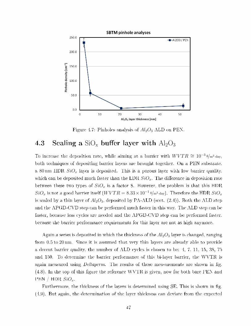
Figure 4.7: Pinholes analysis of Al2O3 ALD on PEN.
4.3 Sealing a SiOx bu�er layer with Al2O3
To increase the deposition rate, while aiming at a barrier with WV TR ∼= 10−3 g/m2·day,
both techniques of depositing barrier layers are brought together. On a PEN substrate,
a 80 nm HDR SiOx layer is deposited. This is a porous layer with low barrier quality,
which can be deposited much faster than the LDR SiOx. The di�erence in deposition rate
between these two types of SiOx is a factor 8. However, the problem is that this HDR
SiOx is not a good barrier itself (WV TR = 8.33×10⁻¹ g/m2·day). Therefore the HDR SiOx
is sealed by a thin layer of Al2O3, deposited by PA-ALD (sect. (2.4)). Both the ALD step
and the APGD-CVD step can be performed much faster in this way. The ALD step can be
faster, because less cycles are needed and the APGD-CVD step can be performed faster,
because the barrier performance requirements for this layer are not as high anymore.
Again a series is deposited in which the thickness of the Al2O3 layer is changed, ranging
from 0.5 to 20 nm. Since it is assumed that very thin layers are already able to provide
a decent barrier quality, the number of ALD cycles is chosen to be: 4, 7, 11, 15, 38, 75
and 150. To determine the barrier performance of this bi-layer barrier, the WVTR is
again measured using Deltaperm. The results of these measurements are shown in �g.
(4.8). In the top of this �gure the reference WVTR is given, now for both bare PEN and
PEN / HDR SiOx.
Furthermore, the thickness of the layers is determined using SE. This is shown in �g.
(4.9). But again, the determination of the layer thickness can deviate from the expected
47

Figure 4.8: Results of the WVTR test of a Al2O3 sealing layer on HDR SiOx. PEN isused as a substrate. The test is performed at 40 ºC and 90 % RH
thickness, estimated by the growth rate of Al2O3 ALD. This deviation is strongest for
the thinnest of the Al2O3 layers and can be caused by nucleation inside the pores of the
SiOx, but also has to do with the way the results are �t. Since the refractive indexes of
the SiOx and Al2O3 layers are close to each other (see table (4.1)), they are di�cult to
separate. Therefore the thickness of the reference sample of PEN / HDR SiOx is used as
the thickness of the other samples, so that the thickness of the SiOx layer is �xed and not
�tted when the thickness of the Al2O3 is determined. The thickness of the Al2O3 layer,
however, can also be estimated by the growth speed of Al2O3 on silicon wafer, because
the growth speed is more or less the same on all kinds of substrates.[36] Using a growth
speed of 0.13 nm/cycle, the thickness of the sealing Al2O3 will be around 0.5, 1, 1.5, 2, 5, 10
and 20 nm, respectively.
The results of the Deltaperm water vapor permeation test show that a decent barrier
can already be deposited using 15 cycles of PA-ALD (∼ 2 nm). When depositing such a
thin sealing layer (WV TR = 2.46× 10⁻³ g/m2·day) it is possible to produce a decent barrier
much faster, as well as that it has a barrier performance, which is a factor 2 − 3 better
than that of a single LDR SiOx layer (WV TR ≈ 6× 10⁻³ g/m2·day).
Next to the Deltaperm measurements, the samples are analyzed by a calcium test (Ca
test, sect. (3.2)). For this Ca test, the WVTR is determined at 20 ºC / 50 % RH by
measuring the change in the transmittance of visible light of the calcium deposited on
48

Figure 4.9: SE results of the thickness of the Al2O3 sealing layer on HDR SiOx. PEN wasused as a substrate.
the barriers. An example of how the samples look in a Ca test is shown in �g. (4.10).
The spots on the calcium layer are due to permeation of water vapor through pores of
interconnecting defects in the barrier. The WVTR is measured at places in between these
spots (intrinsic). The measured WVTR is shown in �g. (4.11) and the results of the
analysis on the defects are shown in �g. (4.12).
From the WVTR results of the Ca test it can be concluded that a layer thickness of
∼ 5 nm of Al2O3 (= 38 ALD cycles) delivers the best result. This still results in a factor
> 2 better barrier performance than for the sample of 15 ALD cycles. This is a larger
improvement than for intrinsic WVTR of the Deltaperm, but it can be seen in the same
range, due to the larger errors in the Ca test, e.g. for the sample which had 15 ALD cycles
WV TR = 1.5 ± 1.1 × 10⁻⁵ g/m2·day, while for sample with 38 ALD cycles it is measured
that WV TR = 4.9± 3.9× 10⁻⁶ g/m2·day.
Another point of interest is that the WVTR of SiNx encapsulation layer itself is close
to the results the barrier layers. Therefore it is reasonable that the calcium on top of the
barriers is also oxidized by permeation through the encapsulation layer. The WVTR of the
barriers might be lower than the WVTR values shown in �g. (4.11). A subtraction of the
reference measurements - which can give a rough estimate of the barrier performance itself
- could then lead to a WVTR of the barrier of ∼ 1×10⁻⁶ g/m2·day. As was mentioned in the
introduction this is the target quality of a barrier, which can be used as a barrier for �exible
electronics. This target value, however, is an extrinsic value of the WVTR of a barrier.
49
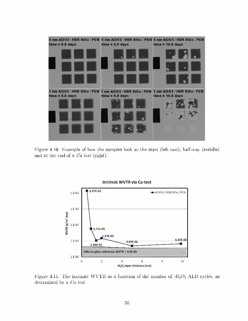
Figure 4.10: Example of how the samples look at the start (left two), half-way (middle)and at the end of a Ca test (right).
Figure 4.11: The intrinsic WVTR as a function of the number of Al2O3 ALD cycles, asdetermined by a Ca test.
50

Figure 4.12: The number of pinholes (structures of interconnecting nano-defects) as afunction of the number of Al2O3 ALD cycles, as determined by a Ca test.
So by comparing the results of the Ca test to the target WVTR of ∼ 1×10⁻⁶ g/m2·day, it is
assumed that the intrinsic quality of the barrier can be deposited over larger areas, without
defects or pinholes. This can be a hard task, but by careful cleaning of the samples and
deposition in ultra clean environments this might be possible. This is shown by Carcia et
al. but also by internal research at Fuji�lm.[4, 8]
When taking a look at the number of defects, this number drops signi�cantly when
sealing the HDR SiOx layer with only ∼ 1.5 nm of Al2O3 (= 11 ALD cycles) and becomes
lower than the SiNx encapsulation layer. This behavior was also seen at the Deltaperm
measurements, although it was not as clear there, the WVTR already started to drop
signi�cantly. The number of defects might even be lower, because of particle contamination
(dust) during the sample transport. The sealing could than be counteracted.
A last important point in �g. (4.11) and �g. (4.12) is about the sample on which
Al2O3 was deposited during 11 ALD cycles (WV TR = 1.1× 10⁻⁵ g/m2·day). This sample is
produced after all other measurements on the extrinsic WVTR were performed, since it
appeared to be in a critical region where the WVTR drops drastically within the range of
a few extra ALD cycles of Al2O3. For the extrinsic WVTR this is no problem, since these
measurements are performed relatively quick after the deposition of the sample. For the
Ca test, however, all measurements are performed at the same time, while this speci�c
sample much later. (The time between the deposition and the actual start of the Ca test
was 45 days for sample with 11 ALD cycles, while for the other samples that time was
51
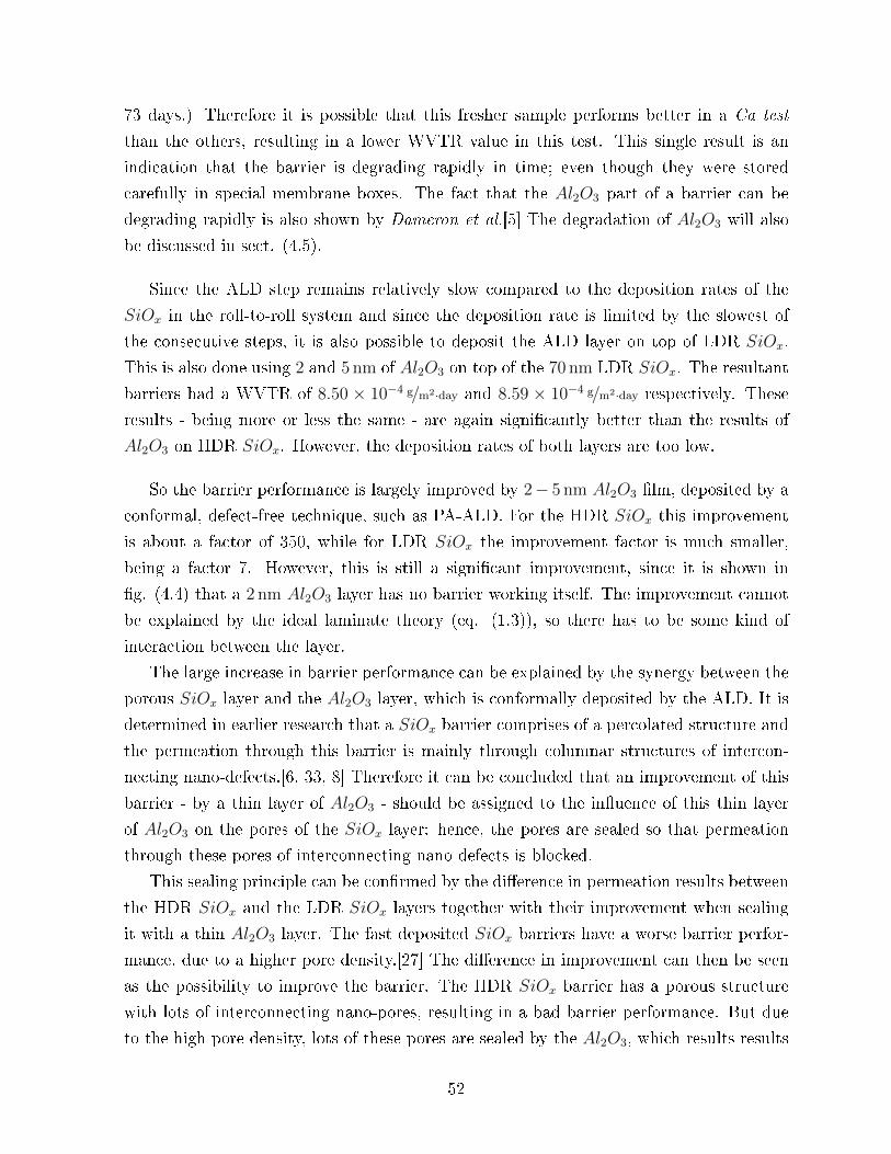
73 days.) Therefore it is possible that this fresher sample performs better in a Ca test
than the others, resulting in a lower WVTR value in this test. This single result is an
indication that the barrier is degrading rapidly in time; even though they were stored
carefully in special membrane boxes. The fact that the Al2O3 part of a barrier can be
degrading rapidly is also shown by Dameron et al.[5] The degradation of Al2O3 will also
be discussed in sect. (4.5).
Since the ALD step remains relatively slow compared to the deposition rates of the
SiOx in the roll-to-roll system and since the deposition rate is limited by the slowest of
the consecutive steps, it is also possible to deposit the ALD layer on top of LDR SiOx.
This is also done using 2 and 5 nm of Al2O3 on top of the 70 nm LDR SiOx. The resultant
barriers had a WVTR of 8.50 × 10⁻⁴ g/m2·day and 8.59 × 10⁻⁴ g/m2·day respectively. These
results - being more or less the same - are again signi�cantly better than the results of
Al2O3 on HDR SiOx. However, the deposition rates of both layers are too low.
So the barrier performance is largely improved by 2− 5 nm Al2O3 �lm, deposited by a
conformal, defect-free technique, such as PA-ALD. For the HDR SiOx this improvement
is about a factor of 350, while for LDR SiOx the improvement factor is much smaller,
being a factor 7. However, this is still a signi�cant improvement, since it is shown in
�g. (4.4) that a 2 nm Al2O3 layer has no barrier working itself. The improvement cannot
be explained by the ideal laminate theory (eq. (1.3)), so there has to be some kind of
interaction between the layer.
The large increase in barrier performance can be explained by the synergy between the
porous SiOx layer and the Al2O3 layer, which is conformally deposited by the ALD. It is
determined in earlier research that a SiOx barrier comprises of a percolated structure and
the permeation through this barrier is mainly through columnar structures of intercon-
necting nano-defects.[6, 33, 8] Therefore it can be concluded that an improvement of this
barrier - by a thin layer of Al2O3 - should be assigned to the in�uence of this thin layer
of Al2O3 on the pores of the SiOx layer: hence, the pores are sealed so that permeation
through these pores of interconnecting nano-defects is blocked.
This sealing principle can be con�rmed by the di�erence in permeation results between
the HDR SiOx and the LDR SiOx layers together with their improvement when sealing
it with a thin Al2O3 layer. The fast deposited SiOx barriers have a worse barrier perfor-
mance, due to a higher pore density.[27] The di�erence in improvement can then be seen
as the possibility to improve the barrier. The HDR SiOx barrier has a porous structure
with lots of interconnecting nano-pores, resulting in a bad barrier performance. But due
to the high pore density, lots of these pores are sealed by the Al2O3, which results results
52
Figure 4.13: Illustration of the sealing of pores by ALD. The porous structure of theSiOx layer (left) is �rst �lled by Al2O3 (middle). When depositing more layers conformallayer-by-layer growth will smoothen the surface. The improvement, however, will not beas large anymore.
in a factor 350 improvement in barrier performance. On the other hand, for the LDR SiOx
layers, there are much less pores - which already results in a decent barrier performance
from the beginning - leaving less pores available for the sealing step of the Al2O3. So in
the case of LDR SiOx, there are less pores present to be sealed, resulting in a smaller
improvement in barrier performance. Next to that, it is assumed that the defects in LDR
SiOx barrier layers are much larger, which makes them harder to seal with a thin layer of
Al2O3.[8]
When looking back to �g. (4.6), the existence of a critical sealing layer thickness can
be explained. Since nucleation of the Al2O3 layer starts inside the pores of the SiOx layer.
It then takes a few ALD cycles before layer by layer growth will start. The pores are
really sealed when the growth process has reached layer by layer growth. As shown in �g.
(4.13), the growth process starts by nucleation inside the pores. After that the pores are
sealed by a process which consequently lowers the pore diameter. After a critical number
of ALD cycles, the pore diameter has become so small that H2O cannot permeate through
it. It appears that most pores have a diameter < 5 nm, since after ∼ 15 cycles of ALD
sealing, the WVTR has dropped drastically. This pore size is con�rmed by Erlat et al.[6]
4.4 In�uence of longer oxygen plasma exposure
In order to further lower the WVTR and to obtain a better insight in the sealing and
nucleation processes, the oxygen plasma exposure time in the ALD cycle is increased up
to 10 s (instead of 2 s). When using a longer oxygen plasma exposure time, the carbon
content in the ALD �lm will decrease, as shown in research done at Eindhoven University.
This is proven by varying the oxygen plasma exposure time and the determination of the
carbon content via RBS (Rutherford Back-scattering spectrometry) measurements. By
lowering the carbon content in the �lm, the structure of the Al2O3 will be more crystalline
and it would contain less defects (lattice defects). Therefore the WVTR can be lower by
53
enlarging the oxygen plasma exposure time.
At Eindhoven University it has been measured that for Al2O3 layers with a thickness
of 100 nm the increase of the oxygen plasma exposure time from 2 s to 10 s resulted in a
lower carbon content, going from 2.5±1.0 at.% for the standard ALD process, to < 1 at.%
for the ALD process in which the oxygen plasma step in enlarged up to 10 s.
In order to determine the in�uence of this longer oxygen plasma exposure step, again
the WVTR is determined and compared to WVTR of the samples of the previous section.
This is both done for the extrinsic WVTR (Deltaperm measurements, sect. (3.1)) and the
intrinsic WVTR (Ca test, (3.2)). From these results, more insight will be gained on the
nucleation process of Al2O3 layers on top of HDR SiOx, deposited by PE-CVD.
First, measurements are performed on the extrinsic WVTR. The results are shown in
�g. (4.14). In this graph, the results of the samples with a 10 s oxygen plasma exposure
time in each ALD cycle are compared to the samples which are deposited by the standard
ALD step times. It can be seen that for thick layers of Al2O3 (5 nm) the barrier of both
series is about the same. The di�erence in carbon content does not lead to a signi�cant
improvement of the barrier quality. However, for thin sealing layers there is a nice im-
provement. Especially for the sample which was exposed to 11 ALD cycles (∼ 1.5 nm).
For the standard deposition process this sample was at the critical thickness, where the
WVTR dropped drastically, but for longer oxygen plasma exposure times, the WVTR
already dropped to the low WVTR regime. With this deposition process, the 11 cycles
of Al2O3 ALD are already enough to seal the pores of the HDR SiOx, while with the
standard deposition process it was not possible.
The second method which is used to analyze the result of enlarging the oxygen plasma
exposure time is a Ca test. In this test, the intrinsic WVTR of the samples is determined
as well as that the number of pores of interconnecting defects can be determined. These
defects are the main pathway of the permeation of water vapor. The results of that are
shown in �g. (4.15) and (4.16). Again these results are compared to the samples which
were deposited at standard ALD conditions.
From �gures (4.14), (4.15) and (4.16) it can be concluded that for thin (1 − 1.5 nm)
Al2O3 layers there is a signi�cant improvement in the barrier performance. Both the
extrinsic WVTR (Deltaperm) and the intrinsic WVTR (Ca test) are decreased, as well as
the number of pathways allowing permeation (pinholes or pores of interconnecting defects).
For the samples which were exposed to more ALD cycles (15 − 38 cycles ∼= 2 − 5 nm),
however, the WVTR values and the number of defects are the same within the error of the
measurements. Since the in�uence of a reduced carbon content would show up especially
54

Figure 4.14: Extrinsic WVTR, as determined by Deltaperm measurements. The results ofthe samples with the enlarged oxygen plasma exposure are shown in light blue (diamonds).As a reference the results of the standard samples are shown (dark blue, squares).
Figure 4.15: Intrinsic WVTR, as determined by Ca test measurements. The results of thesamples with the enlarged oxygen plasma exposure are shown in light blue (diamonds).As a reference the results of the standard samples are shown (dark blue, squares).
55
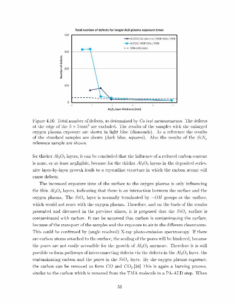
Figure 4.16: Total number of defects, as determined by Ca test measurements. The defectsat the edge of the 5 × 5 mm2 are excluded. The results of the samples with the enlargedoxygen plasma exposure are shown in light blue (diamonds). As a reference the resultsof the standard samples are shown (dark blue, squares). Also the results of the SiNx
reference sample are shown.
for thicker Al2O3 layers, it can be concluded that the in�uence of a reduced carbon content
is none, or at least negligible, because for the thicker Al2O3 layers in the deposited series,
nice layer-by-layer growth leads to a crystalline structure in which the carbon atoms will
cause defects.
The increased exposure time of the surface to the oxygen plasma is only in�uencing
the thin Al2O3 layers, indicating that there is an interaction between the surface and the
oxygen plasma. The SiOx layer is normally terminated by −OH groups at the surface,
which would not react with the oxygen plasma. Therefore, and on the basis of the results
presented and discussed in the previous alinea, it is proposed that the SiOx surface is
contaminated with carbon. It can be assumed that carbon is contaminating the surface,
because of the transport of the samples and the exposure to air in the di�erent cleanrooms.
This could be con�rmed by (angle resolved) X-ray photo-emission spectroscopy. If there
are carbon atoms attached to the surface, the sealing of the pores will be hindered, because
the pores are not easily accessible for the growth of Al2O3 anymore. Therefore it is still
possible to form pathways of interconnecting defects via the defects in the Al2O3 layer, the
contaminating carbon and the pores in the SiOx layer. By the oxygen plasma exposure,
the carbon can be removed to form CO and CO2.[34] This is again a burning process,
similar to the carbon which is removed from the TMA molecule in a PA-ALD step. When
56

the surface is exposed to the oxygen plasma for a longer time, more carbon can be removed,
resulting in a better sealing of the pores.
4.5 Pore analysis via activation energy
In the last section of this chapter on the results of the experiments - and the discussion
about it - the activation energy of the barriers is determined. The activation energy
can provide information on the pore structure of the barrier[6] as well as that it can
be used to determine the barrier performance at ambient conditions - 20 ºC / 50 %
relative humidity (RH) - from the results at elevated temperatures.[4] In order to further
research the barrier structure, together with the determination of the barrier performance
at ambient conditions, these activation energy experiments are performed, using a barrier
of HDR SiOx, sealed with 2 nm of Al2O3, deposited with a longer oxygen plasma exposure
time in the oxidizing step of the ALD cycle, as extensively explained in the previous section.
In the activation energy experiments, the logarithm of the WVTR values is plotted as
a function of the inversed temperature. Such a plot is called an Arrhenius plot, leaving
the slope of this plot linearly related to the activation energy, as shown in eq. (1.5). In the
�rst part of this section, the activation energy is determined, using WVTR measurements
at 40, 50, 60 and 70 ºC, while in the second part the extrapolation to ambient conditions
is done.
In the �rst part of this section, the activation energy is determined via the determina-
tion of the WVTR at 40 to 70 ºC. The results are shown in �g. (4.17), using WVTR values
of 1.83, 5.44, 13.2 and 23.4 ×10⁻³ g/m2·day at temperatures of 40, 50, 60 and 70 ºC.
A linear �t of these results (also shown) and the use of eq. (1.5), then leads to our activa-
tion energy, ∆Eact ≈ 76 kJ/mole. However, it can be seen that for the higher temperature
measurement points, the WVTR value (and their logarithm) is slightly lower than ex-
pected. Unexpected WVTR values at higher temperatures can be a result of the physical
contact between the samples and the box they are placed in. The �lms get deformed due
to the high pressure di�erence between the high pressure and low pressure side of the
Deltaperm (up to 500 Torr).
The apparent activation energy can also be used to determine the water vapor transmis-
sion rate at other conditions, e.g. at 20 ºC. This is done in �g. (4.18). After subtraction
of the aluminum permeation results, the activation energy could again be determined.
Following this procedure, a higher activation energy is determined of ∆Eact ≈ 82 kJ/mole.
This can be used to extrapolate to 20 ºC and 90 % RH, resulting the WVTR to be
WV TR = 1.93 × 10⁻⁴ g/m2·day. Using this results, it is also possible determine the water
57
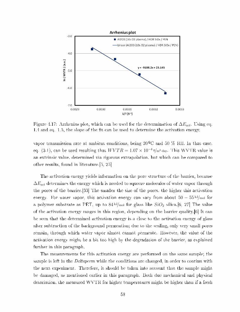
Figure 4.17: Arrhenius plot, which can be used for the determination of ∆Eact. Using eq.1.4 and eq. 1.5, the slope of the �t can be used to determine the activation energy.
vapor transmission rate at ambient conditions, being 20 ºC and 50 % RH. In that case,
eq. (3.1), can be used resulting that WV TR = 1.07× 10⁻⁴ g/m2·day. This WVTR value is
an extrinsic value, determined via rigorous extrapolation, but which can be compared to
other results, found in literature.[5, 25]
The activation energy yields information on the pore structure of the barrier, because
∆Eact determines the energy which is needed to squeeze molecules of water vapor through
the pores of the barrier.[33] The smaller the size of the pores, the higher this activation
energy. For water vapor, this activation energy can vary from about 50 − 55 kJ/mol for
a polymer substrate as PET, up to 84 kJ/mol for glass like SiO2 silica.[6, 27] The value
of the activation energy ranges in this region, depending on the barrier quality.[6] It can
be seen that the determined activation energy is a close to the activation energy of glass
after subtraction of the background permeation; due to the sealing, only very small pores
remain, through which water vapor almost cannot permeate. However, the value of the
activation energy might be a bit too high by the degradation of the barrier, as explained
further in this paragraph.
The measurements for this activation energy are performed on the same sample; the
sample is left in the Deltaperm while the conditions are changed, in order to continu with
the next experiment. Therefore, it should be taken into account that the sample might
be damaged, as mentioned earlier in this paragraph. Both due mechanical and physical
detoriation, the measured WVTR for higher temperatures might be higher than if a fresh
58

Figure 4.18: Using ∆Eact after the subtraction of the aluminum foil tests, the WVTR canbe extrapolated. This results in an activation energy of ∆Eact ≈ 82 kJ/mole and a WVTRof 1.93× 10⁻⁴ g/m2·day at 20 ºC and 90 % RH.
sample would be measured. The possible damaging of the samples is mainly for the higher
tempearture, these values are determined after the measurements at lower temperatures.
Due to the high vapor pressure at these elevated temperatures the sample might bend,
which can cause cracks in the barrier layer, as well as that the sample can physically touch
the setup, damaging the very thin Al2O3 layer (2 nm).
On the other hand it is possible that the Al2O3 layer is deteriorating by the pres-
ence of water vapor.[5] Via an exothermic reaction, Al2O3 + 3H2O → 2Al(OH)3, a more
amorphous structure might be formed, resulting in a higher WVTR. In the experiment
by Dameron et al.[5] this deterioration of the Al2O3 layer only shows up when this layer
is directly exposed to water vapor, while no deterioration is seen when the backside of
the barrier is exposed to water vapor. The latter situation is the same as for the results
presented here. However, barrier performance of the polymer substrate and the HDR
SiOx layer is bad and the Al2O3 layer is very thin. Therefore, this e�ect cannot be fully
excluded and should be researched further. Espescially if one keeps in mind that the
presented barrier should protect devices from water vapour and when doing so, they are
exposed to water vapor.
Due to these to deteriation mechanisms, the barrier will perform worse at higher tem-
peratures. The measured activation energy might therefore be too high. However, it
still stands that the �nal barrier (consisting of both HDR SiOx and Al2O3) has only very
59

narrow pores of permeation, because pores of the HDR SiOx layer are sealed by the Al2O3.
60

�
61

Chapter 5
Conclusions & Recommendations
In this project it is shown that it is possible to increase the deposition rate of SiOx barrier
layers, together with an increase in barrier performance. This is the result of the switch
from LDR SiOx to HDR SiOx. When sealing this HDR SiOx with a thin layer of Al2O3,
the higher deposition rate can be accompanied by a low WVTR.
With this technique, it is shown that only 15 ALD cycles of Al2O3 (∼ 2 nm) are enough
to decrease the WVTR down to 2.46× 10⁻³ g/m2·day. This is an increase in barrier perfor-
mance of a factor 350 compared to bare HDR SiOx on PEN and a factor 2-3 improvement
compared to LDR SiOx (WVTR =6.21× 10⁻³ g/m2·day). The factor 350 improvement can-
not be explained by ideal-laminate-theory.[27]
The switch from LDR SiOx to HDR SiOx also leads to a large improvement in de-
position rate. The SiOx layers can be deposited 8 times faster. The sealing with Al2O3
ALD, however, is a relatively slow deposition technique, which can only be used because
very thin layers of Al2O3 are obtained. The current ALD deposition process is also too
slow, but with the use of spatial ALD, problems with the growth speed of ALD (see eq.
(2.11)) can be overcome.[24]
The large increase in barrier performance by a thin �lm of Al2O3, deposited by ALD,
can be explained by the sealing of the interconnected nano-pores of the HDR SiOx layer.
This sealing is possible because the HDR SiOx consists of grains, while at the edges of these
grains, nano-pores are present. Permeation of water vapor is allowed by the interconnection
of those nano-pores. Blocking of these interconnected nano-pores, prevents water vapor
from permeating through the barrier. Permeation is forced through the intrinsic material,
which results in a drop in the WVTR.
The drop in WVTR after a critical thickness, is observed after ∼ 2 nm for the extrinsic
WVTR, but also for the intrinsic WVTR and the number of macro-defects and intercon-
62
nected nano-pores. It is also shown that the WVTR of the intrinsic material can reach
∼ 1× 10⁻⁶ g/m2·day.
Furthermore, this critical thickness decreases if the oxygen plasma exposure time in
the ALD cycle is increased from 2.0 s to 10.0 s. On the other hand, when more ALD cycles
are used, there is no change observed in the WVTR or the number of macro-defects and
remaining interconnected nano-pores. This indicates that there is carbon present at the
interface between the HDR SiOx bu�er layer and the Al2O3 sealing layer. The oxygen
plasma helps to remove the carbon, which improves the sealing of the interconnected
nano-pores.
The sealing of the pores is also shown by the activation energy of the deposited barriers.
For standard SiOx barriers, deposited by CVD, ∆Eact ranges from 50− 55 kJ/mol for poor
barriers (depending on the substrate) up to 84 kJ/mol for ideal glass-like SiOx barriers.[6]
Although the barriers, as deposited in this research, are not purely SiOx barriers, their
activation energy (∆Eact = 82 kJ/mol) shows that the pores are sealed e�ciently. Because
this ∆Eact is close to the ideal value of SiOx barriers, it can be concluded that the number
of pathways through which di�usion of water vapor is possible is decreased.
At last, this activation energy is used to determined the WVTR at atmospheric con-
ditions (20 ºC and 50 % RH). Using rigorous extrapolations of the WVTR values as mea-
sured by Deltaperm at elevated temperatures, it can be determined that the WVTR at
atmospheric conditions is 1.07× 10⁻⁴ g/m2·day.
Outlook
Further understanding of this sealing principle is important in its application for the de-
position of barriers layers. Therefore, other measurements are proposed to proof and to
understand the sealing of the pores in HDR SiOx. After the deposition of the sealing
layer, Angle-Resolved X-Ray Photo-emission Spectroscopy (AR-XPS) measurements are
proposed, so that the penetration of the Al2O3 into the pores of the SiOx can be deter-
mined and compared to other bu�er layers (e.g. LDR SiOx or silicon wafer). Next to
that, if the Al2O3 is sealing the pores on the inside (as shown in �g. (4.13)), for the �rst
ALD cycles the increase in mass of the samples should be larger. This mass increase could
be measured in-situ by a quartz crystal microbalance (QCM). Various polymer substrates
were already researched, using this method.[36]
On the other hand, as discussed in sect. (4.5), also the degradation of the Al2O3
sealing layers should be taken into account. It is suggested that they degrade relatively
quickly.[5] This should also be researched before a production process of barrier layers can
take place. This can be researched by exposing the barriers to water vapor for longer times
63

or at higher temperatures.
Part of the increase in barrrier performance by a thin Al2O3 layer might also explained
by the fact that the SiOx layer works as a planarizing layer. When depositing Al2O3 by
ALD on polymer substrates, nucleation of the Al2O3 can take place inside the substrate.[36]
Therefore, more cycles are needed to obtain nice layer-by-layer growth with ALD. If the
SiOx layer can work as a planarizing layer, none or much less nucleation can take place
inside the layer, while the conformal, defect-free growth can start directly. In this way
a thin Al2O3 can work much better as a barrier layer. This e�ect will also play a role,
although it is not really likely that just 2 nm of Al2O3 works as such a good barrier.
A better understanding of the sealing principle can lead to an increase in barrier per-
formance. Next to that, it is shown that it is very important to keep the samples clean[4],
especially between the deposition of the bu�er layer and the sealing layer. Particle con-
tamination will lead to worse sealing, which decreases the barrier performance. Therefore
extremely clean transport should be considered or both deposition steps should be per-
formed roll-to-roll, so that particle contamination is reduced largely.
For the carbon contamination by the exposure to air, as discussed is sect. (4.4), it
should be researched if a cleaning process is possible, using an oxygen plasma, in order to
remove all carbon and carbon containing materials. A better sealing of the pores becomes
possible in this way, which increases the barrier performance.
With this research, I hope that Fuji�lm can continue to increase the performance of
their barrier layers, so that they can work as protection layers for �exible electronics in
the future.
64

�
65
Appendix A
WVTR Measurement values after
aluminum foil experiments
It is explained in sec. (3.1) that the WVTR values, as measured by Deltaperm, are
actually lower than the results shown in chap. (4). Experiments are performed using a
100µm aluminum foil, to determine the permeation for an approximately impermeable
foil. The remaining permeation is an estimate for the o�set or leakage of the Deltaperm
setup. In this appendix, the results are shown after subtraction of this o�set. The o�set is
(3.6±0.5)×10−4g/m2·day. Unless it is mentioned otherwise, the measurements are performed
at our standard conditions, 40 ºC and 90 % RH.
The outline of this chapter will be the same as in chap. (4). This means the WVTR
results of the single layer barriers will be discussed �rst. After that, the WVTR results of
the HDR SiOx barriers which are sealed with a thin layer of Al2O3; �rst in the standard
ALD process and later with an enlarged oxygen plasma exposure time. The last part that
will be discussed is the e�ect of this leakage on the determination o the activation energy.
Single layer barrier results In sect. (4.2), three di�erent barriers were discussed: LDR
SiOx, HDR SiOx and Al2O3. Each of them has an optimal thickness and an associated
deposition rate. These properties are shown in �g. (A.1), together with the original
WVTR, as measured by Deltaperm, and WVTR corrected for leakage permeation. Only
the results on PEN substrate are shown. It can be seen that for barriers with a large
permeation the in�uence of this leakage is negligable, while for really good barrier their is
a real in�uence.
Barriers with a sealing layer Further in this research, bi-layer barriers are discussed.
In this case the HDR SiOx is sealed with a thin layer of Al2O3. This sealing process
66

Figure A.1: Original and corrected WVTR results of the single barrriers investigated inthis research. Also their optimal thickness and associated deposition rate is shown.
results in a barrier with good barrier properties, but which can also be deposited much
faster than the standard LDR SiOx (a factor 8). The Al2O3 sealing layer is very thin
(≤ 5 nm), so that this layer can also be deposited relatively fast. ALD is a relatively slow
deposition technique, but since the sealing is very thin, deposition can still be performed
quickly. The sealing procedure of the HDR SiOx layer with Al2O3 results in a barrier
performance of 1.48× 10⁻³ g/m2·day for a ∼ 5 nm sealing layer. When using a sealing layer
of ∼ 20 nm, this can even go down to 8.50× 10⁻⁴ g/m2·day. These results are shown in �g.
(A.2). The results are shown as a function of the number of ALD cycles. The growth rate
per cycle is determined to be 0.13 nm/cycle.
Using looxygen plasma exposure times in ALD cycle Also for the permeation
experiments on the samples which are deposited with a longer oxygen plasma time step
in the ALD cycle the WVTR can be corrected for small leakages is the Deltaperm system.
The results of that are shown in �g. A.3: for a ∼ 5 nm sealing layer, the WVTR is
now improved to 1.35× 10⁻³ g/m2·day. Also the improvement for the sample at the critical
thickness of ∼ 1.5 nm is improved even further.
Activation energy The last measurements which are in�uenced by leakages, measured
by testing the permeation of an impermeable aluminum foil, are the measurements for the
determination of the activation energy. However, in order to make a correct extrapolation
67

Figure A.2: Al2O3 on HDR SiOx on PEN
Figure A.3: longer plasma times
68

of theWVTR results to room temperature, the WVTR results at elavated temperatures are
already corrected for this leakages. Therefore, as shown in �g. (4.18), using this correction,
the WVTR at 20 °C is 1.93× 10⁻⁴ g/m2·day . This is determined with ∆Eact ≈ 82 kJ/mole.
69

Bibliography
[1] E. Aldea, P. Peeters, H. De Vries, and M.C.M Van De Sanden. Atmospheric glow
stabilization. do we need pre-ionization? Surface and Coatings Technology, 200:46�50,
October 2005.
[2] G. Aresta, P. A. Premkumar, S. A. Starostin, H. de Vries, M. C. M. van de Sanden,
and M. Creatore. Optical characterization of plasma-deposited sio(2)-like layers on
anisotropic polymeric substrates. Plasma Processes and Polymers, 7(9-10):766�774,
October 2010.
[3] P. F. Carcia, R. S. McLean, M. D. Groner, A. A. Dameron, and S. M. George. Gas
di�usion ultrabarriers on polymer substrates using al(2)o(3) atomic layer deposition
and sin plasma-enhanced chemical vapor deposition. Journal of Applied Physics,
106(2):023533, July 2009.
[4] P.F. Carcia, R.S. McLean, M.H. Reilly, M.D. Groner, and S.M. George. Ca test of
al2o3 gas di�usion barriers grown by atomic layer deposition on polymers. Applied
Physics Letters, 89(3):031915, July 2006.
[5] A. A. Dameron, S. D. Davidson, B. B. Burton, P. F. Carcia, R. S. McLean, and S. M.
George. Gas di�usion barriers on polymers using multilayers fabricated by al2o3 and
rapid sio2 atomic layer deposition. Journal of Physical Chemistry C, 112(12):4573�
4580, March 2008.
[6] A. G. Erlat, R. J. Spontak, R. P. Clarke, T. C. Robinson, P. D. Haaland, Y. Trop-
sha, N. G. Harvey, and E. A. Vogler. Siox gas barrier coatings on polymer sub-
strates: Morphology and gas transport considerations. Journal of Physical Chemistry
B, 103(29):6047�6055, July 1999.
[7] A. G. Erlat, B. C. Wang, R. J. Spontak, Y. Tropsha, K. D. Mar, D. B. Montgomery,
and E. A. Vogler. Morphology and gas barrier properties of thin siox coatings on poly-
70

carbonate: Correlations with plasma-enhanced chemical vapor deposition conditions.
Journal of Materials Research, 15(3):704�717, March 2000.
[8] Fuji�lm. Private communication.
[9] S.M. George. Atomic layer deposition: An overview. Chemical Reviews, 110(1):111�
131, January 2010.
[10] M. D. Groner, S. M. George, R. S. McLean, and P. F. Carcia. Gas di�usion barriers on
polymers using al2o3 atomic layer deposition. Applied Physics Letters, 88(5):051907,
January 2006.
[11] G.J.M. Hagelaar and L.C. Pitchford. Solving the boltzmann equation to obtain elec-
trond transport coe�ciets and rate coe�cients for �uid models. Plasma Sources Sci-
ence and Technology, 14:722�733, October 2005.
[12] S. B. S. Heil, P. Kudlacek, E. Langereis, R. Engeln, M. C. M. van de Sanden, and
W. M. M. Kessels. In situ reaction mechanism studies of plasma-assisted atomic layer
deposition of al2o3. Applied Physics Letters, 89(13):131505, September 2006.
[13] T. O. Kaariainen, P. Maydannik, D. C. Cameron, K. Lahtinen, P. Johansson, and
J. Kuusipalo. Atomic layer deposition on polymer based �exible packaging materials:
Growth characteristics and di�usion barrier properties rid e-7955-2010. Thin Solid
Films, 519(10):3146�3154, March 2011.
[14] W.M.M. Kessels. Avs 58th international symposium & exhibition. In Plasma-
enhanced CVD & ALD prepared nanolayers for high e�ciency solar cells, November
2011.
[15] W. Keuning, P. van de Weijer, H. Lifka, W.M.M. Kessels, and M. Creatore. Cathode
encapsulation of oleds by atomic layer deposited al2o3 �lms and al2o3/a-sinx:h stacks.
2011.
[16] H. C. M. Knoops, E. Langereis, M. C. M. van de Sanden, and W. M. M. Kessels.
Conformality of plasma-assisted ald: Physical processes and modeling. Journal of the
Electrochemical Society, 157(12):G241�G249, 2010.
[17] Ulrich Kogelschatz. Dielectric-barrier discharges: Their history, discharge physics,
and industrial applications. Plasma Chemistry and Plasma Processing, 23(1):1�46,
March 2003. 10.1023/A:1022470901385.
71

[18] E. Langereis. Plasma-assisted atomic layer deposition. PhD thesis, Eindhoven, Uni-
versity of Technology, 2008.
[19] E. Langereis, M. Creatore, S. B. S. Heil, M. C. M. Van de Sanden, and W. M. M.
Kessels. Plasma-assisted atomic layer deposition of al2o3 moisture permeation barri-
ers on polymers. Applied Physics Letters, 89(8):081915, August 2006.
[20] J. S. Lewis and M. S. Weaver. Thin-�lm permeation-barrier technology for �exible or-
ganic light-emitting devices. Ieee Journal of Selected Topics In Quantum Electronics,
10(1):45�57, January 2004.
[21] Y. F. Liew, H. Aziz, N. X. Hu, H. S. O. Chan, G. Xu, and Z. Popovic. Investigation
of the sites of dark spots in organic light-emitting devices. Applied Physics Letters,
77(17):2650�2652, October 2000.
[22] W.L. Morgan, C. Winstead, and V. McKoy. Electron collision cross sections for
tetraethoxysilane. Journal of Applied Physics, 92(3):1663�1667, August 2002.
[23] Holger Norenberg. Permeation measurements at 0.001 g/m2/day and below for ap-
plications in �exible electronics. Paper. Technolox Ltd.
[24] P. Poodt, A. Lankhorst, F. Roozeboom, K. Spee, D. Maas, and A. Vermeer. High-
speed spatial atomic-layer deposition of aluminum oxide layers for solar cell passiva-
tion. Advanced Materials, 22(32):3564�+, August 2010.
[25] P. A. Premkumar, S. A. Starostin, M. Creatore, H. de Vries, R. M. J. Pa�en, P. M.
Koenraad, and M. C. M. van de Sanden. Smooth and self-similar sio(2)-like �lms
on polymers synthesized in roll-to-roll atmospheric pressure-pecvd for gas di�usion
barrier applications. Plasma Processes and Polymers, 7(8):635�639, August 2010.
[26] P. A. Premkumar, S. A. Starostin, H. de Vries, R. M. J. Pa�en, M. Creatore, T. J.
Eijkemans, P. M. Koenraad, and M. C. M. van de Sanden. High quality sio(2)-like
layers by large area atmospheric pressure plasma enhanced cvd: Deposition process
studies by surface analysis. Plasma Processes and Polymers, 6(10):693�702, October
2009.
[27] A. P. Roberts, B. M. Henry, A. P. Sutton, C. R. M. Grovenor, G. A. D. Briggs,
T. Miyamoto, A. Kano, Y. Tsukahara, and M. Yanaka. Gas permeation in silicon-
oxide/polymer (siox/pet) barrier �lms: role of the oxide lattice, nano-defects and
macro-defects. Journal of Membrane Science, 208(1-2):75�88, October 2002.
72

[28] Robin Roelofs. Optical analysis (se and ftir-atr) of silicon oxide �lms on pen substrates
by atmospheric pressure barrier discharge deposition. Report, Summer 2010.
[29] S. A. Starostin, P. A. Premkumar, M. Creatore, E. M. van Veldhuizen, H. de Vries,
R. M. J. Pa�en, and M. C. M. van de Sanden. On the formation mechanisms of
the di�use atmospheric pressure dielectric barrier discharge in cvd processes of thin
silica-like �lms. Plasma Sources Science & Technology, 18(4):045021, November 2009.
[30] S. A. Starostin, P. Antony Premkumar, M. Creatore, H. de Vries, R. M. J. Pa�en,
and M. C. M. van de Sanden. High current di�use dielectric barrier discharge in
atmospheric pressure air for the deposition of thin silica-like �lms. Applied Physics
Letters, 96(6):061502�061502�3, 2010.
[31] S.A. Starostin, M.A.M. ElSabbagh, E. Aldea, H. de Vries, M. Creatore, and M.C.M.
van de Sanden. Formation and expansion phases of an atmospheric pressure glow
discharge in a pecvd reactor via fast iccd imaging. Plasma Science, IEEE Transactions
on DOI - 10.1109/TPS.2008.924622, 36(4):968�969, 2008.
[32] S. Starostine, E. Aldea, H. de Vries, M. Creatore, and M. C. M. van de Sanden.
Atmospheric pressure barrier discharge deposition of silica-like �lms on polymeric
substrates. Plasma Processes and Polymers, 4:S440�S444, April 2007.
[33] Y. G. Tropsha and N. G. Harvey. Activated rate theory treatment of oxygen and
water transport through silicon oxide poly(ethylene terephthalate) composite barrier
structures. Journal of Physical Chemistry B, 101(13):2259�2266, March 1997.
[34] T. J. VINK, M. M. J. VANZANDVOORT, O. L. J. GIJZEMAN, and J. W. GEUS.
The interaction of oxygen and carbon-monoxide with a carbided ni(111) surface.
Applied Surface Science, 18(3):255�267, 1984.
[35] Y. Widjaja and C.B. Musgrave. Quantum chemical study of the mechanism of alu-
minum oxide atomic layer deposition. Applied Physics Letters, 80(18):3304�3306,
May 2002.
[36] C. A. Wilson, R. K. Grubbs, and S. M. George. Nucleation and growth during
al2o3 atomic layer deposition on polymers. Chemistry of Materials, 17(23):5625�
5634, November 2005.
[37] Hugh D. Young and Roger A. Freedman. University Physics. Addison Wesley, 11th
edition, 2004.
73