effects of aln thickness on structural and transport properties of in-rich...
TRANSCRIPT

Effects of AlN thickness on structural and transport properties of In-rich n-AlInN/AlN/p-Si(0 0 1)
heterojunctions grown by magnetron sputtering
This article has been downloaded from IOPscience. Please scroll down to see the full text article.
2013 J. Phys. D: Appl. Phys. 46 095106
(http://iopscience.iop.org/0022-3727/46/9/095106)
Download details:
IP Address: 129.173.72.87
The article was downloaded on 14/03/2013 at 09:32
Please note that terms and conditions apply.
View the table of contents for this issue, or go to the journal homepage for more
Home Search Collections Journals About Contact us My IOPscience

IOP PUBLISHING JOURNAL OF PHYSICS D: APPLIED PHYSICS
J. Phys. D: Appl. Phys. 46 (2013) 095106 (7pp) doi:10.1088/0022-3727/46/9/095106
Effects of AlN thickness on structuraland transport properties of In-richn-AlInN/AlN/p-Si(0 0 1) heterojunctionsgrown by magnetron sputteringH F Liu, S B Dolmanan, S Tripathy, G K Dalapati, C C Tan and D Z Chi
Institute of Materials Research and Engineering (IMRE), A*STAR (Agency for Science, Technology andResearch), 3 Research Link, Singapore 117602, Singapore
E-mail: [email protected]
Received 31 October 2012, in final form 18 December 2012Published 7 February 2013Online at stacks.iop.org/JPhysD/46/095106
AbstractWe have studied the effect of AlN buffer layers, having variable thicknesses in situ grown byrf-magnetron sputtering, on the structural and vibration dynamic properties of AlInN thin filmsgrown by dc-magnetron sputtering on Si(0 0 1) substrates at 700 ◦C. X-ray diffraction patternsreveal that an increase in thickness of the AlN buffer layer can significantly promote thetextured growth orientation of AlInN(0 0 0 2)//Si(0 0 1) and improve the grain sizes of AlInN.They also reveal that the Al composition in the resultant AlInN thin film increases with thethickness of AlN; however, phase separations, which are usually observed in metal-organicchemical vapour deposition (MOCVD) growth of AlInN with similar Al compositions, are notdetectable. Instead, uniform element distribution profiles along the growth direction of AlInNare detected by secondary ion-mass spectroscopy. Micro-Raman scattering spectra collected atroom temperature exhibit three optical phonon features from the AlInN thin films, which, interms of their evolutions with Al composition, can be assigned to AlInN EH
2 , InN-like A1(LO),and AlN-like A1(LO), respectively, consistent with that recently observed in MOCVD grownIn-rich AlInN. The solar cell based on n-AlInN/AlN/p-Si exhibits a typical diode-like darkI–V curve; however, its photocarrier collection is apparently suppressed due to thepolarization charges at the junction interfaces.
(Some figures may appear in colour only in the online journal)
1. Introduction
Driven by applications in high-electron-mobility transistor(HEMTs) [1], photovoltaic (PV) devices [2], and thermoelec-tric devices [3, 4], growth and investigation of AlInN thin filmshave been attracting more research interest [5–8]. Wang et alhave studied the effect of source flux and growth tempera-ture on indium incorporation behaviour of AlInN alloys bymolecular beam epitaxy (MBE) [9]. Yamamoto’s group hasinvestigated the effect of gas flow on the growth and phase sep-aration of AlInN by metal-organic chemical vapour deposition(MOCVD) [10]. In general, it is quite challenge to obtainhigh-quality AlInN thin films with indium composition larger
than ∼32%. One of the reasons is that the equilibrium vapourpressure of InN is much higher than that of AlN, and AlInNalloys with high indium composition tend to phase separate,resulting in variations of alloy composition in the resultantthin film. To suppress the phase separation of high-indium-content AlInN, physical vapour growth techniques, such asMBE, pulsed laser deposition (PLD) and sputter-deposition,operating under conditions far from equilibrium may haveadvantages over MOCVD.
When compared with MBE and PLD, the sputter-deposition technique is much cheaper, which also has theadvantage in scaling-up, e.g., in thin film PV industry. Ourrecent studies, as well as those reports from different groups
0022-3727/13/095106+07$33.00 1 © 2013 IOP Publishing Ltd Printed in the UK & the USA

J. Phys. D: Appl. Phys. 46 (2013) 095106 H F Liu et al
[5, 6], revealed that in magnetron-sputter deposition of AlInN,radio-frequency (rf), i.e. a power supplying configuration, isover direct current (dc) for achieving higher crystal qualityunder, otherwise, the same growth conditions. However, thegrowth rate of AlInN by rf-magnetron sputtering is much lowerthan that by dc-magnetron sputtering. Both are related tothe variations in voltage–current match for the metal targets.To combine both the advantages, in this work, we havestudied AlInN growth by dc-magnetron sputtering employingAlN buffer layers that were in situ grown by rf-magnetronsputtering, addressing the effect of the AlN thickness. Forthese studies, we have employed x-ray diffraction (XRD),secondary ion mass spectroscopy (SIMS) and micro-Ramanscattering technologies.
2. Experimental
Al (99.999%) and Al/In alloy (50 : 50 wt%, 99.99%) targets,both 4 inch in diameter, were used as the source materials forgrowing AlN and AlInN, respectively. A mixture of nitrogenand argon (both are 99.999% in purity and 5 sccm in flow-rate) was used as the working gas as well as the source ofnitrogen reactive species. The working pressure was kept5.0 mTorr throughout the whole growth stage. Both the rfpower on the Al target and the dc power on the Al/In targetwere set at 100 W, controlled by individual auto-matchingpower units. Under these growth conditions, the growthrate of AlInN, obtained by cross-sectional scanning electronmicroscopy (SEM), is ∼3.5 nm min−1, about 5 times fasterthan that of AlN. Si (0 0 1) substrates, before loading intothe growth chamber, were etched by buffered hydrofluoridesolution, washed by de-ionized water, and dried by nitrogenflow to remove the native oxide skin layer. Four AlInN/AlN/Sithin film samples, having the same AlInN thickness (∼170 nm)but different nominal AlN thicknesses (tAlN = 3.75, 7.5, 15,30 nm labelled samples A, B, C and D, respectively), weregrown for comparisons in this study. Both the AlN bufferlayer and the AlInN thin film were grown at 700 ◦C in thesame sputter chamber without growth interruption.
3. Results and discussion
3.1. Structural characterization
Figure 1(a) presents the XRD spectra collected from samples Ato D, showing that (i) polycrystalline AlInN were grown in thethin film samples, (ii) there is no priority in growth orientationsof AlInN for samples A and B with tAlN � 7.5 nm, (iii) onsetof preferential growth orientation of AlInN (0 0 0 2)//Si (0 0 1)occurred in sample C with tAlN = 15 nm, (iv) the AlInN(0 0 0 2)//Si (0 0 1) orientated growth is further promoted fromsamples C to D by an increase in the AlN thickness (i.e. from15 to 30 nm) and (v) diffractions from the AlN buffer layers arenot detectable due to their small thicknesses as well as Al/Inatoms interdiffusion across the interface of AlInN/AlN (seelatter discussions). XRD pole-figure measurements, shownin figure 1(b), confirm that the AlInN of sample D consistsof fibre-textured grains with AlInN (0 0 0 2)//Si (0 0 1). This
Figure 1. (a) XRD spectra collected from samples A to D, the insetplots the AlInN (0 0 0 2) peak angle and line width as a function ofAlN thickness; (b) XRD pole-figure measurements aiming at AlInN(0 0 0 2) and (1 0 −1 1) atomic planes.
is evidenced by the fact that the pole-figure recorded aroundAlInN (0 0 0 2) atomic planes only exhibits a peak located atϕ = 0◦; meanwhile, the pole-figure recorded around AlInN(1 0 −1 1) atomic planes only exhibit a ring-distribution ataboutϕ = 60◦, corresponding to the angle between the (0 0 0 2)and (1 0 −1 1) atomic planes in hexagonal wurtzite crystals,without any preferential distribution in the φ axis.
In general, thin film growth by magnetron-sputterdeposition starts from crystal nucleation/seeding, which isfollowed by island growth and coalescence driven by reductionof surface and strain energies1. Island growth in thin filmis an orientation selective process, which strongly dependson the deposition temperature, the growth rate, and the filmthickness. In the case of III-nitrides, which have close-packedatomic planes along their c-axis, to minimize the surfaceand grain boundary energies, (0 0 0 2)-textured islands, when
1 Surface energies remain on the island surface and grain boundaries whilethe strain energies are associated with individual islands due to island growth.
2

J. Phys. D: Appl. Phys. 46 (2013) 095106 H F Liu et al
approaching a certain size, tend to dominate over others inthe film growth. This is indeed what we have observed forAlN growth in figure 1(a) since the growth conditions and thethickness of AlInN are exactly the same for samples A–D. Ithas to be noted that direct growths of 90 nm AlInN or AlN on Si(0 0 1) by rf-magnetron sputtering under similar conditions alsoresult in the fibre-textured structure of AlInN(0 0 0 2)//Si(0 0 1)and AlN(0 0 0 2)//Si(0 0 1) [11]. These observations suggestthat the random distribution in grain orientations resulted inthe dc-magnetron sputtering (e.g. for tAlN < 15 nm in thisstudy) is mainly caused by the higher growth rate, whichsuppresses the movement of adatoms on the islands at a certaingrowth temperature, and as a result, the section of island growthorientation is suppressed.
A careful look at the diffraction peaks in figure 1(a)reveals that when tAlN is increased, the AlInN (0 0 0 2) peakshifts to higher angles, accompanied by peak strengtheningand narrowing. The inset in figure 1(a) plots the peak positionand full-width at half-maximum (FWHM) of AlInN (0 0 0 2)as a function of tAlN. The values were derived by peak fittingsusing the Gaussian function. One can see that the AlInN(0 0 0 2) angle (2θ) monotonically increases while its line-width monotonically decreases with the thickness of AlN.The high-angular shift of AlInN (0 0 0 2) manifests itself asan increase in Al composition. The decrease in line-width,together with the increase in peak intensity, indicates theimprovement in crystal quality, typically the increase in grainsize, of the resultant AlInN. Cross-sectional scanning-electronmicroscopy (SEM) (not shown here for the sake of brevity)revealed columnar grains of sample A with the average in-planegrain size of ∼35 nm. With the help of the Scherrer formula,together with the XRD data in figure 1(a), one can estimatethe average in-plane grain size for samples B–D (for whichrecording of a high-quality SEM image is quite a challengedue to the charging effect). The estimation revealed that theaverage in-plane grain sizes of samples A–D increased from35 to 41 nm. The Al compositions derived from the AlInN(0 0 0 2) diffraction angles and Vegard’s law are 46.0%, 51.2%,54.2% and 57.1% for samples A, B, C and D, respectively.It should be noted that these values could be overestimatedsince island coalescence tends to induce tensile strain into thenitride films and the larger the grain sizes resulted in the largerstrain induced. On the other hand, cooling down from thegrowth temperature (i.e. 700 ◦C) also causes tensile strain intothe AlInN thin films due to the thermal expansion coefficientmismatch between nitride and Si. Unfortunately, we are notable to measure the film strain due to the small thicknesses.Nevertheless, the increase in Al composition from samples Ato D has been further confirmed by SIMS measurements andRaman scattering.
The origin of the increase in Al composition is not clearat this stage. It could be caused by, for example, targetcontamination, surface segregation and atoms interdiffusion.During AlN growth, the Al/In alloy target could becontaminated with Al deposited on its surface. An increasein the growth time of AlN will lead to more Al depositedon the Al/In target and thus more Al incorporated into thefollowing AlInN growth. Segregation of In atoms towards the
Figure 2. SIMS depth-profiles of Al, In, N, and Si collected fromAlInN/AlN/Si(0 0 1) thin film samples: (a) sample A, (b) sample B,(c) sample C and (d) sample D. The circles indicate the presence ofthe AlN buffer layer while the arrow in (d) indicates the atominterdiffusions across the interface of AlInN/AlN.
growing surface due to the large size mismatch between In andAl atoms [12], together with the increased grain sizes, and alsothe crystal strain, from samples A to D, might also contribute tothe increase in Al composition. Atoms interdiffusion of In/Alacross the AlInN/AlN interface, driven by the compositionalgradations under a ‘self-annealing’ condition, could transfer Alfrom AlN into AlInN and In backwards during the followinggrowth of AlInN.
Presented in figure 2 are the depth profiles of Al, In,N and Si measured by SIMS from samples A to D. It isseen that Al, In, and N are relatively uniform in distributionsthroughout the AlInN layer, supporting the absence of AlInNphase separations. The remarkable differences among samplesA–D are found at the interface between AlInN and Si (markedby circles in figure 2), where AlN buffer layers were grownwith increased thicknesses from samples A to D. The clearlydeveloped step in the In profile of sample D, indicated by thearrow in figure 2(d), provides evidence for the diffusion of Inatoms from AlInN into the AlN buffer layer. This, togetherwith the small thickness, leads to the fact that diffractionsfrom the AlN buffer layers are undetectable in figure 1(a).Figure 3 presents a detailed analysis of the SIMS results bycomparing the Al-to-In intensity ratios among samples A–D.One can see that the Al-to-In SIMS intensity ratio increasesmonotonically from samples A to D, indicating the increasein Al composition from samples A to D, which is consistentwith the XRD analysis. However, it has to be noted that
3

J. Phys. D: Appl. Phys. 46 (2013) 095106 H F Liu et al
Figure 3. SIMS intensity ratio of Al-to-In obtained from the SIMSdepth profiles, showing the increase in aluminum composition fromsamples A to D.
the absolute composition ratios of Al-to-In are not obtainablefrom the SIMS intensity analysis due to the lack of elementalyield factors of In and Al in the studied AlInN thin filmmaterials [13].
3.2. Raman scattering spectroscopy
Figure 4(a) shows the micro-Raman spectra collected fromsamples A to D at room temperature using a 488 nm laserexcitation in a backscattering configuration. Three Ramanfeatures, originated from the AlInN layers, can be resolvedby spectrum fittings employing the Lorentzian function. Atypical example is shown in the inset in figure 4(a), wherethe spectrum (collected from sample A) is well fitted by threepeaks labelled P1, P2 and P3, respectively. The Raman shifts,derived from the spectrum fittings of samples A–D, are plottedin figure 4(b) as a function of Al composition. The dashed linesin figure 4(b) represent the EH
2 and A1(LO) modes of stress-free InN and AlN. One can clearly see that all the three Ramanmodes of AlInN nearly linearly increase with the increase inAl compositions. This behaviour is the same as those reportedby Kang et al [10]. In terms of the phonon behaviours ofthe widely investigated InGaN and AlGaN ternary alloys, theP1 and P3 features are readily assigned to EH
2 and AlN-likeA1(LO) modes.
For the feature of P2, it increases from smaller to largerthan the stress-free value of AlN-EH
2 with the increase in Alcomposition from 46.0% to 57.1%. This behaviour is mostunlikely of AlN-like EH
2 because both the incorporation of Inand the tensile strain in the AlInN film would decrease P2 to besmaller than the stress-free value of AlN-EH
2 (see figure 4(b)).Alternatively, it can be assigned to InN-like A1(LO) mode andin this case, the alloying of Al into InN significantly increasesP2 while the effect of tensile strain is negligible, which isconsistent with those reported by Kang et al [8, 10]. Thisresult confirms that the mode-splitting behaviour induced byalloying in AlInN is different from those in InGaN and AlGaN,where the A1(LO) exhibits a single-mode behaviour while theEH
2 exhibits a two-mode behaviour.
Figure 4. (a) Micro-Raman spectra collected at room temperaturefrom samples A to D, the inset shows a typical spectrum fitting,from which three Raman features originated from AlInN, labelledP1, P2 and P3, are resolved; (b) Raman shifts of the three Ramanfeatures as a function of aluminum composition, from which theRaman features of P1, P2 and P3 can be assigned to EH
2 , InN-likeA1(LO), and AlN-like A1(LO), respectively.
3.3. Electrical transport characterization
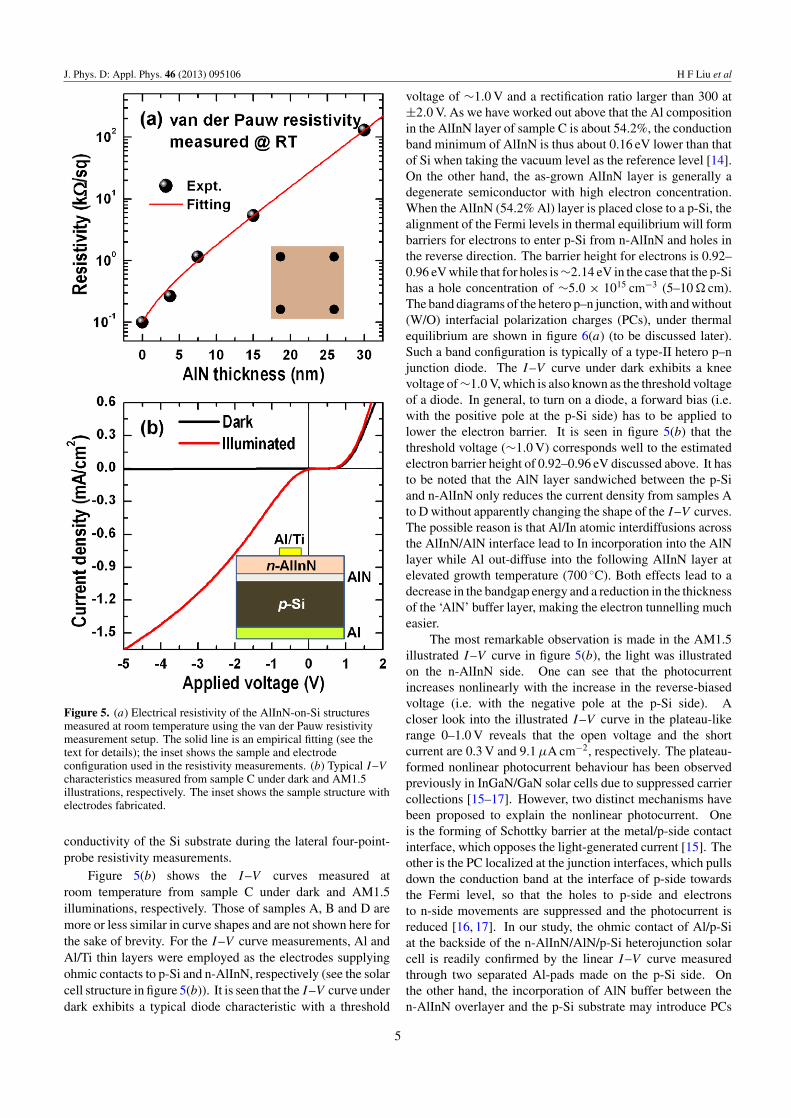
Figure 5(a) presents the electrical resistivity measured from areference n-AlInN/p-Si sample without AlN buffer (see [11])and the n-AlInN/AlN/p-Si samples A–D with various AlNthicknesses. The measurements were carried out at roomtemperature using the van der Pauw resistivity measurementsetup (see the inset in figure 5(a) for the square samplegeometry with contacts inside the perimeter). It is seen thatthe resistivity monotonically increases with the increase in AlNthickness. The solid curve in figure 5(a) is an empirical fittingto the experiment data, which reveals a nearly exponentialbehaviour of the resistivity, i.e. ρ ∝ exp(αt), where t is thethickness of AlN and α is a fitting parameter. For the bestfitting in figure 5(a), α = 0.21 nm−1. Since the AlInN layers,especially those of samples A–D, were grown under exactlythe same conditions and had almost the same thicknesses,the increase in resistivity must be caused by the increase inAlN thickness. The increase in resistivity as a function ofAlN thickness in samples A–D is clearly attributable to theinsulator character of AlN, which tends to decouple the shunt
4
J. Phys. D: Appl. Phys. 46 (2013) 095106 H F Liu et al
Figure 5. (a) Electrical resistivity of the AlInN-on-Si structuresmeasured at room temperature using the van der Pauw resistivitymeasurement setup. The solid line is an empirical fitting (see thetext for details); the inset shows the sample and electrodeconfiguration used in the resistivity measurements. (b) Typical I–Vcharacteristics measured from sample C under dark and AM1.5illustrations, respectively. The inset shows the sample structure withelectrodes fabricated.
conductivity of the Si substrate during the lateral four-point-probe resistivity measurements.
Figure 5(b) shows the I–V curves measured atroom temperature from sample C under dark and AM1.5illuminations, respectively. Those of samples A, B and D aremore or less similar in curve shapes and are not shown here forthe sake of brevity. For the I–V curve measurements, Al andAl/Ti thin layers were employed as the electrodes supplyingohmic contacts to p-Si and n-AlInN, respectively (see the solarcell structure in figure 5(b)). It is seen that the I–V curve underdark exhibits a typical diode characteristic with a threshold
voltage of ∼1.0 V and a rectification ratio larger than 300 at±2.0 V. As we have worked out above that the Al compositionin the AlInN layer of sample C is about 54.2%, the conductionband minimum of AlInN is thus about 0.16 eV lower than thatof Si when taking the vacuum level as the reference level [14].On the other hand, the as-grown AlInN layer is generally adegenerate semiconductor with high electron concentration.When the AlInN (54.2% Al) layer is placed close to a p-Si, thealignment of the Fermi levels in thermal equilibrium will formbarriers for electrons to enter p-Si from n-AlInN and holes inthe reverse direction. The barrier height for electrons is 0.92–0.96 eV while that for holes is ∼2.14 eV in the case that the p-Sihas a hole concentration of ∼5.0 × 1015 cm−3 (5–10 � cm).The band diagrams of the hetero p–n junction, with and without(W/O) interfacial polarization charges (PCs), under thermalequilibrium are shown in figure 6(a) (to be discussed later).Such a band configuration is typically of a type-II hetero p–njunction diode. The I–V curve under dark exhibits a kneevoltage of ∼1.0 V, which is also known as the threshold voltageof a diode. In general, to turn on a diode, a forward bias (i.e.with the positive pole at the p-Si side) has to be applied tolower the electron barrier. It is seen in figure 5(b) that thethreshold voltage (∼1.0 V) corresponds well to the estimatedelectron barrier height of 0.92–0.96 eV discussed above. It hasto be noted that the AlN layer sandwiched between the p-Siand n-AlInN only reduces the current density from samples Ato D without apparently changing the shape of the I–V curves.The possible reason is that Al/In atomic interdiffusions acrossthe AlInN/AlN interface lead to In incorporation into the AlNlayer while Al out-diffuse into the following AlInN layer atelevated growth temperature (700 ◦C). Both effects lead to adecrease in the bandgap energy and a reduction in the thicknessof the ‘AlN’ buffer layer, making the electron tunnelling mucheasier.
The most remarkable observation is made in the AM1.5illustrated I–V curve in figure 5(b), the light was illustratedon the n-AlInN side. One can see that the photocurrentincreases nonlinearly with the increase in the reverse-biasedvoltage (i.e. with the negative pole at the p-Si side). Acloser look into the illustrated I–V curve in the plateau-likerange 0–1.0 V reveals that the open voltage and the shortcurrent are 0.3 V and 9.1 µA cm−2, respectively. The plateau-formed nonlinear photocurrent behaviour has been observedpreviously in InGaN/GaN solar cells due to suppressed carriercollections [15–17]. However, two distinct mechanisms havebeen proposed to explain the nonlinear photocurrent. Oneis the forming of Schottky barrier at the metal/p-side contactinterface, which opposes the light-generated current [15]. Theother is the PC localized at the junction interfaces, which pullsdown the conduction band at the interface of p-side towardsthe Fermi level, so that the holes to p-side and electronsto n-side movements are suppressed and the photocurrent isreduced [16, 17]. In our study, the ohmic contact of Al/p-Siat the backside of the n-AlInN/AlN/p-Si heterojunction solarcell is readily confirmed by the linear I–V curve measuredthrough two separated Al-pads made on the p-Si side. Onthe other hand, the incorporation of AlN buffer between then-AlInN overlayer and the p-Si substrate may introduce PCs
5

J. Phys. D: Appl. Phys. 46 (2013) 095106 H F Liu et al
Figure 6. (a) Band diagram of the n-AlInN/AlN/p-Si heterojunctionwith and without (W/O) polarization charges (PC) at the interfacesand (b) spectral response of the n-AlInN/AlN/p-Si heterojunctionsolar cell under zero and −5 V biases.
at the n-AlInN/AlN and the AlN/p-Si interfaces due to thelarge spontaneous and piezoelectric polarization effects ofAlN. In this case, an energy barrier for holes to reach p-Siside thorough the junction area is induced by the interfacialPCs (see figure 6(a) for the band diagram).
Figure 6(b) shows the spectral responses of then-AlInN/AlN/p-Si heterojunction solar cell under zero- and−5 V biases, respectively. In fact, we could not observe anyapparent spectral responses for small biases, suggesting thatthe collection of photocarriers is ineffective due to the existenceof interfacial PCs. This result is consistent with the I–V curvedunder illumination in figure 5(b). As a comparison, when thebias is increased, e.g., to −5 V, the barrier for photogeneratedholes near the junction area to reach p-Si side can be overcome.In consequence, the spectral response, from both the Si andAlInN of the heterojunction, is significantly increased. Inthis regard, we can make a conclusion that the nonlinear
photocurrent behaviour observed in the n-AlInN/AlN/p-Sisolar cell is mainly due to the effect of PCs localized atthe junction interfaces, which prevent the photocarriers fromeffective collection. As a result, the photocurrent is reduced,especially at lower biases.
4. Conclusion
In conclusion, AlN thin film with various thicknesses,nominally ranging from 3.75 nm to 30 nm, in situ grownby rf-magnetron sputtering at 700 ◦C were used as thebuffer layer for the following growth of AlInN thin filmby dc-magnetron sputtering at the same temperature. It isfound that under certain conditions, the growth of AlInN bydc-magnetron sputtering on Si (0 0 1) with AlN thicknessessmaller than 15 nm resulted in polycrystalline film without anypreferential growth orientations. An increase in AlN thicknessto larger than 15 nm led to the fibre-textured growth ofAlInN(0 0 0 2)//Si(0 0 1). Meanwhile, increases in aluminumcomposition and grain size of the AlInN thin film with theincrease in AlN thickness are observed without any crystalphase separations. Three Raman features are detected from theAlInN thin film, they nearly lineally increase with aluminumcompositions and, in terms of their Raman shifts, can beassigned to EH
2 , InN-like A1(LO), and AlN-like A1(LO),respectively. The alloying induced mode behaviour in AlInNis different from those of the widely investigated InGaN andAlGaN alloys, where EH
2 splits into InN-like and AlN-likemodes while A1(LO) is a single mode. For photovoltaicapplications, the n-AlInN/AlN/p-Si solar cell exhibits a typicaldiode I–V curve under dark with the rectification ratio largerthan 300 at ±2.0 V. However, the photocarrier collection isapparently suppressed when compared with those of the solarcells without employing the AlN buffer layer, which is mainlyattributed to the polarization charges localized at the junctioninterfaces.
References
[1] Kirste L, Lim T, Aidam R, Muller S, Waltereit P andAmbacher O 2010 Phys. Status Solidi a 207 1338
[2] Yamamoto A, Islam Md R, Kang T T and Hashimoto A 2010Phys. Status Solidi c 7 1309
[3] Tong H, Zhang J, Liu G Y, Herbsommer J A, Huang G S andTansu N 2010 Appl. Phys. Lett. 97 112105
[4] Yamaguchi S, Izaki R, Kaiwa N, Sugimura S and Yamamoto A2004 Appl. Phys. Lett. 84 5344
[5] He H, Cao Y, Fu R L, Guo W, Huang Z, Wang M L,Huang C G, Huang J Q and Wang H 2010 Appl. Surf. Sci.256 1812
[6] Han Q F, Duan C G, Du G P, Shi W Z and Ji L C 2010 J.Electron. Mater. 39 489
[7] Aschenbrenner T, Dartsch H, Kruse C, Anastasescu M,Stoica M, Gartner M, Pretourius A, Rosenauer A, Wagner Tand Hommel D 2010 J. Appl. Phys. 108 063533
[8] Kang T T, Hashimoto A and Yamamoto A 2009 Phys. Rev. B79 033301
[9] Wang Z Y, Shi B M, Cai Y, Wang N and Xie M H 2010 J.Appl. Phys. 108 033503
[10] Kang T T, Yamamoto M, Tanaka M, Hashimoto A andYamamoto A 2009 J. Appl. Phys. 106 053525
[11] Liu H F, Tan C C, Dalapati G K and Chi D Z 2012 J. Appl.Phys. 112 063114
6

J. Phys. D: Appl. Phys. 46 (2013) 095106 H F Liu et al
[12] Cosendey G, Carlin J F, Kaufmann N A K, Butte R andGrandjean N 2011 Appl. Phys. Lett. 98 181111
[13] Liu H F, Xiang N and Chua S J 2006 J. Cryst. Growth290 24
[14] Jones R E, Broesler R, Yu K M, Ager J W III, Haller E E,Walukiewicz W, Chen X and Schaff W J 2008 IEEEPhotovoltaic Specialist Conf. (San Diego, CA) 1–4
[15] Jani O, Ferguson I, Honsberg C and Kurtz S 2007 Appl. Phys.Lett. 91 132117
[16] Li Z Q, Lestradet M, Xiao Y G and Li S 2011 Phys. StatusSolidi a 208 928
[17] Neufeld C J, Cruz S C, Farrell R M, Iza M, Lang J R, Keller S,Nakamura S, DenBaars S P, Speck J S and Mishra U K2011 Appl. Phys. Lett. 98 243507
7