eel-4713 ann gordon-ross 1 eel-4713 computer architecture memory hierarchies
TRANSCRIPT

EEL-4713 Ann Gordon-Ross 1
EEL-4713Computer Architecture
Memory hierarchies

EEL-4713 Ann Gordon-Ross 2
The Motivation for Caches
° Motivation:
• Large memories (DRAM) are slow
• Small memories (SRAM) are fast
° Make the average access time small by:
• Servicing most accesses from a small, fast memory.
° Reduce the bandwidth required of the large memory
Processor
Memory System
Cache DRAM

EEL-4713 Ann Gordon-Ross 3
Outline of Today’s Lecture
° Introduction to Memory Hierarchies & caches
° Cache write and replacement policies

EEL-4713 Ann Gordon-Ross 4
*An Expanded View of the Memory System
Control
Datapath
Memory
Processor
Mem
ory
Memory
Memory
Mem
ory
Fastest Slowest
Smallest Biggest
Highest Lowest
Speed:
Size:
Cost:

EEL-4713 Ann Gordon-Ross 5
The Principle of Locality
Address Space0 memsize
Probabilityof reference
What are the principles of Locality?

EEL-4713 Ann Gordon-Ross 6
The Principle of Locality
° The Principle of Locality:
• Program access a relatively small portion of the address space at any instant of time.
• Example: 90% of time in 10% of the code
° Two Different Types of Locality:
• Temporal Locality (Locality in Time): If an item is referenced, it will tend to be referenced again soon.
• Spatial Locality (Locality in Space): If an item is referenced, items whose addresses are close by tend to be referenced soon.
Address Space0 memsize
Probabilityof reference

EEL-4713 Ann Gordon-Ross 7
Memory Hierarchy: Principles of Operation
° 2-level hierarchy example
° At any given time, data is copied between only 2 adjacent levels:
• Upper Level (Cache) : the one closer to the processor
- Smaller, faster, and uses more expensive technology
• Lower Level (Memory): the one further away from the processor
- Bigger, slower, and uses less expensive technology
° Block:
• The minimum unit of information that can either be present or not present in the two-level hierarchy
Lower Level(Memory)Upper Level
(Cache)To Processor
From ProcessorBlk X
Blk Y

EEL-4713 Ann Gordon-Ross 8
Memory Hierarchy: Terminology
° Hit: data appears in some block in the upper level (example: Block X)
• Hit Rate: the fraction of memory accesses found in the upper level
• Hit Time: Time to access the upper level which consists of
RAM access time + Time to determine hit/miss
° Miss: data needs to be retrieved from a block in the lower level (Block Y)
• Miss Rate = 1 - (Hit Rate)
• Miss Penalty = Time to replace a block in the upper level +
Time to deliver the block the processor
° Hit Time << Miss PenaltyLower Level
(Memory)Upper Level(Cache)
To Processor
From ProcessorBlk X
Blk Y

EEL-4713 Ann Gordon-Ross 9
Basic Terminology: Typical Values
Typical Values
Block (line) size 4 - 128 bytes
Hit time 1 - 4 cycles
Miss penalty 10 - 100 cycles (and increasing)
Miss rate 1% - 20%
Cache Size 64 KB - 8 MB
EEL-4713 Ann Gordon-Ross 10
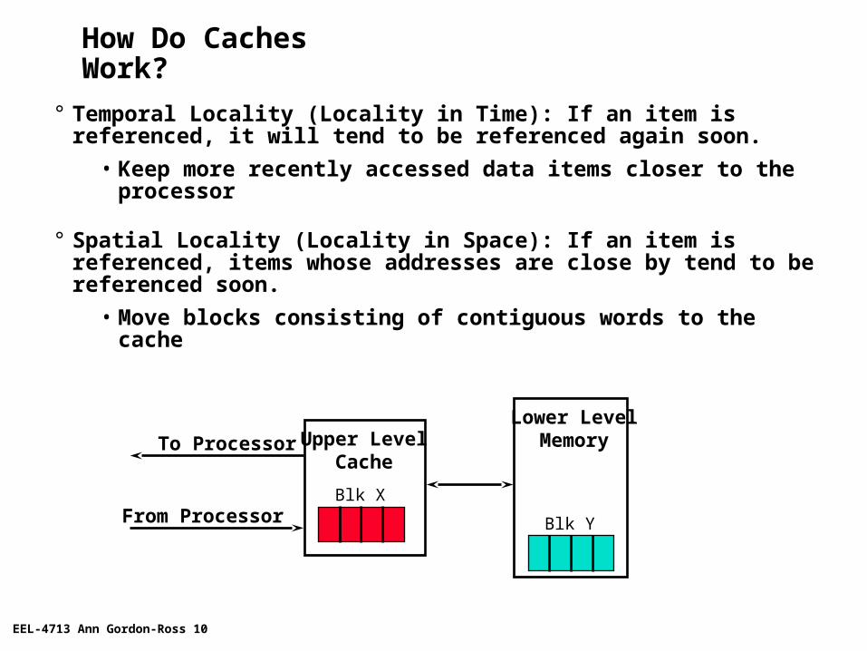
How Do Caches Work?
° Temporal Locality (Locality in Time): If an item is referenced, it will tend to be referenced again soon.
• Keep more recently accessed data items closer to the processor
° Spatial Locality (Locality in Space): If an item is referenced, items whose addresses are close by tend to be referenced soon.
• Move blocks consisting of contiguous words to the cache
Lower LevelMemoryUpper Level
CacheTo Processor
From ProcessorBlk X
Blk Y

EEL-4713 Ann Gordon-Ross 11
The Simplest Cache: Direct-Mapped Cache
Memory
4 Byte Direct Mapped Cache
Memory Address
0
1
2
3
4
5
6
7
8
9
A
B
C
D
E
F
Cache Index
0
1
2
3
° Location 0 can be occupied by data from:
• Memory location 0, 4, 8, ... etc.
• In general: any memory locationwhose 2 LSBs of the address are 0s
• Address<1:0> => cache index
° How can we tell which block is in the cache?
• Valid bit
• Tag

EEL-4713 Ann Gordon-Ross 12
Cache Tag and Cache Index
° Assume a 32-bit memory (byte) address:
• A 2^N bytes direct mapped cache:
- Cache Index: The lower N bits of the memory address
- Cache Tag: The upper (32 - N) bits of the memory address
Cache Index
0
1
2
3
2 - 1N
:
2 N BytesDirect Mapped Cache
Byte 0
Byte 1
Byte 2
Byte 3
Byte 2**N -1
0N31
:
Cache Tag Example: 0x50 Ex: 0x03
0x50
Stored as partof the cache “state”Valid Bit
:

EEL-4713 Ann Gordon-Ross 13
Cache Access Example
Access 000 01
Start Up
000 M [00001]
Access 010 10
(miss)
(miss)
000 M [00001]
010 M [01010]
Tag DataV
000 M [00001]
010 M [01010]
Miss Handling:Load DataWrite Tag & Set V
Load Data
Write Tag & Set V
Access 000 01(HIT)
000 M [00001]
010 M [01010]Access 010 10(HIT)
° Caches begin empty:
• A lot of misses at start up:
Compulsory Misses
- (Cold start misses)

EEL-4713 Ann Gordon-Ross 14
Definition of a Cache Block
° Cache Block (cache “line”): cache data that has its own cache tag
° Our previous “extreme” example:
• 4-byte Direct Mapped cache: Block Size = 1 Byte
• Takes advantage of Temporal Locality: If a byte is referenced,it will tend to be referenced soon.
• Did not take advantage of Spatial Locality: If a byte is referenced, its adjacent bytes will be referenced soon.
° In order to take advantage of Spatial Locality: increase the block size
Direct Mapped Cache Data
Byte 0
Byte 1
Byte 2
Byte 3
Cache TagValid

EEL-4713 Ann Gordon-Ross 15
Example: 1 KB Direct Mapped Cache with 32 B Blocks
° For a 2 ** N byte cache:
• The uppermost (32 - N) bits are always the Cache Tag
• The lowest M bits are the Byte Select (Block Size = 2 ** M)
Cache Index
0
1
2
3
:
Cache Data
Byte 0
0431
:
Cache Tag Example: 0x50
Ex: 0x01
0x50
Stored as partof the cache “state”
Valid Bit
:
31
Byte 1Byte 31 :
Byte 32Byte 33Byte 63 :Byte 992Byte 1023 :
Cache Tag
Byte Select
Ex: 0x00
9

EEL-4713 Ann Gordon-Ross 16
Block size tradeoffs
° Larger block helps with spatial locality
° However, transferring a large block from memory to cache takes longer than transferring a small block
• “miss penalty”
° Important to understand implication of block sizes in the average time to service a memory request
° Average memory access time (AMAT)
• Hit_time * (1 – miss_rate) + miss_rate*miss_penalty
° Cache design goals:
• Short hit time
• Small miss rate
• Short miss penalty

EEL-4713 Ann Gordon-Ross 17
Components of miss penalty
Control
Datapath
Memory
Processor
Mem
ory
Memory
Memory
Mem
ory
Memory latency:depends on memory size,technologyTransfer time:
(block size/bus width)*bus cycle
Penalty latency + transfer time

EEL-4713 Ann Gordon-Ross 18
*Block Size Tradeoff
° In general, larger block size take advantage of spatial locality BUT:
• Larger block size means larger miss penalty:
- Takes longer time to fill up the block
• If block size is too big relative to cache size, miss rate will go up
° Average Access Time:
• = Hit Time x (1 - Miss Rate) + Miss Penalty x Miss Rate
MissPenalty
Block Size
MissRate Exploits Spatial Locality
Fewer blocks: compromisestemporal locality
AverageAccess
Time
Increased Miss Penalty& Miss Rate
Block Size Block Size

EEL-4713 Ann Gordon-Ross 19
Another Extreme Example
° Cache Size = 4 bytes Block Size = 4 bytes
• Only ONE entry in the cache
° If an item is accessed, likely that it will be accessed again soon
• But it is unlikely that it will be accessed again immediately!!!
• The next access will likely to be a miss again
- Continually loading data into the cache butdiscard (force out) them before they are used again
° Conflict Misses are misses caused by:
• Different memory locations mapped to the same cache index
- Solution 1: make the cache size bigger
- Solution 2: Multiple entries for the same Cache Index
0
Cache DataValid Bit
Byte 0Byte 1Byte 3
Cache Tag
Byte 2

EEL-4713 Ann Gordon-Ross 20
Outline
° Set-associative caches
° Simulation experiments
° Replacement and write policies

EEL-4713 Ann Gordon-Ross 21
*Our original direct-mapped cache
° Implementation diagram
Cache Data
Cache Block 0
Cache TagValid
:: :
Cache Index
Cache Block
CompareAdr Tag
Hit
Cache IndexCache Tag
Address of a lw/sw

EEL-4713 Ann Gordon-Ross 22
A Two-way Set Associative Cache
° N-way set associative: N entries for each Cache Index
• N direct mapped caches operate in parallel
° Example: Two-way set associative cache
• Cache Index selects a “set” from the cache
• The two tags in the set are compared in parallel
• Data is selected based on the tag result
Cache Data
Cache Block 0
Cache TagValid
:: :
Cache Data
Cache Block 0
Cache Tag Valid
: ::
Cache Index
Mux 01Sel1 Sel0
Cache Block
CompareAdr Tag
Compare
OR
Hit
EEL-4713 Ann Gordon-Ross 23
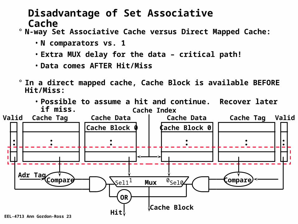
Disadvantage of Set Associative Cache
° N-way Set Associative Cache versus Direct Mapped Cache:
• N comparators vs. 1
• Extra MUX delay for the data – critical path!
• Data comes AFTER Hit/Miss
° In a direct mapped cache, Cache Block is available BEFORE Hit/Miss:
• Possible to assume a hit and continue. Recover later if miss.
Cache Data
Cache Block 0
Cache Tag Valid
: ::
Cache Data
Cache Block 0
Cache TagValid
:: :
Cache Index
Mux 01Sel1 Sel0
Cache Block
CompareAdr Tag
Compare
OR
Hit

EEL-4713 Ann Gordon-Ross 24
Critical path: direct-mapped cache
Cache Data
Cache Block 0
Cache TagValid
:: :
Cache Index
Cache Block
CompareAdr Tag
Hit
Cache IndexCache Tag
Address of a lw/sw
Tag delayData delay

EEL-4713 Ann Gordon-Ross 25
Critical path: Set Associative Cache
Cache Data
Cache Block 0
Cache Tag Valid
: ::
Cache Data
Cache Block 0
Cache TagValid
:: :
Cache Index
Mux 01Sel1 Sel0
Cache Block
CompareAdr Tag
Compare
OR
Hit
Tag delayData delay

EEL-4713 Ann Gordon-Ross 28
A Summary on Sources of Cache Misses
° Compulsory (cold start, first reference): first access to a block
• “Cold” fact of life: not a whole lot you can do about it
° Conflict (collision):
• Multiple memory locations mappedto the same cache location
• Solution 1: increase cache size
• Solution 2: increase associativity
° Capacity:
• Cache cannot contain all blocks access by the program
• Solution: increase cache size
° Invalidation: other process (e.g., I/O, other CPU) updates memory

EEL-4713 Ann Gordon-Ross 29
And yet Another Extreme Example: Fully Associative
° Fully Associative Cache -- push the set associative idea to its limit!
• Forget about the Cache Index
• Compare the Cache Tags of all cache entries in parallel
• Example: Block Size = 2 B blocks, we need N 27-bit comparators
° By definition: Conflict Miss = 0 for a fully associative cache
:
Cache Data
Byte 0
0431
:
Cache Tag (27 bits long)
Valid Bit
:
Byte 1Byte 31 :
Byte 32Byte 33Byte 63 :
Cache Tag
Byte Select
Ex: 0x01
X
X
X
X
X

EEL-4713 Ann Gordon-Ross 30
Making room for a new block
° Direct Mapped Cache:
• Each memory location can only mapped to 1 cache location
• No need to make any decision
- Current item replaced the previous item in that cache location
° N-way Set Associative Cache:
• Each memory location have a choice of N cache locations
° Fully Associative Cache:
• Each memory location can be placed in ANY cache location
° Cache miss in a N-way Set Associative or Fully Associative Cache:
• Bring in new block from memory
• Throw out a cache block to make room for the new block
• Need to make a decision on which block to throw out!

EEL-4713 Ann Gordon-Ross 31
Cache Block Replacement Policy
° Random Replacement:
• Hardware randomly selects a cache item and throws it out
° Least Recently Used:
• Hardware keeps track of the access history
• Replace the entry that has not been used for the longest time
° Example of a Simple “Pseudo” Least Recently Used Implementation:
• Assume 64 Fully Associative Entries
• Hardware replacement pointer points to one cache entry
• Whenever an access is made to the entry the pointer points to:
- Move the pointer to the next entry
• Otherwise: do not move the pointer
:
Entry 0
Entry 1
Entry 63
Replacement
Pointer

EEL-4713 Ann Gordon-Ross 32
*Cache Write Policy: Write Through versus Write Back
° Cache read is much easier to handle than cache write:
• Instruction cache is much easier to design than data cache
° Cache write:
• How do we keep data in the cache and memory consistent?
° Two options (decision time again :-)
• Write Back: write to cache only. Write the cache block to memory when that cache block is being replaced on a cache miss.
- Need a “dirty” bit for each cache block
- Greatly reduce the memory bandwidth requirement
- Control can be complex
• Write Through: write to cache and memory at the same time.
- Isn’t memory too slow for this?

EEL-4713 Ann Gordon-Ross 33
Write Buffer for Write Through
° A Write Buffer is needed between the Cache and Memory
• Processor: writes data into the cache and the write buffer
• Memory controller: write contents of the buffer to memory
° Write buffer is just a FIFO:
• Works fine if: Store frequency (w.r.t. time) << 1 / DRAM write cycle
° However if:
• Store frequency > 1 / DRAM write cycle
• Write buffer saturation
ProcessorCache
Write Buffer
DRAM

EEL-4713 Ann Gordon-Ross 34
Write Buffer Saturation
° Store frequency > 1 / DRAM write cycle
• If this condition exist for a long period of time (CPU cycle time too quick and/or too many store instructions in a row):
- Store buffer will overflow no matter how big you make it
° Solution for write buffer saturation:
• Use a write back cache
• Install a second level (L2) cache:
ProcessorCache
Write Buffer
DRAM
ProcessorCache
Write Buffer
DRAML2Cache

EEL-4713 Ann Gordon-Ross 35
Write Allocate versus Not Allocate
° Assume: a 16-bit write to memory location 0x0 causes a miss
• Do we read in the rest of the block (Bytes 2, 3, ... 31)?
Yes: Write Allocate (usually associated w/ write-back)
No: Write Not Allocate (write-through)
Cache Index
0
1
2
3
:
Cache Data
Byte 0
0431
:
Cache Tag Example: 0x00
Ex: 0x00
0x01
Valid Bit
:
31
Byte 1Byte 31 :
Byte 32Byte 33Byte 63 :Byte 992Byte 1023 :
Cache Tag
Byte Select
Ex: 0x00
9

EEL-4713 Ann Gordon-Ross 36
What is a Sub-block?
° Sub-block:
• A unit within a block that has its own valid bit
• Example: 1 KB Direct Mapped Cache, 32-B Block, 8-B Sub-block
- Each cache entry will have: 32/8 = 4 valid bits
° Write miss: only the bytes in that sub-block are brought in.
0
1
2
3
:
Cache Data
:
SB
0’s
V B
it
:
31
Cache Tag SB
1’s
V B
it
:
SB
2’s
V B
it
:
SB
3’s
V B
it
:
Sub-block0Sub-block1Sub-block2Sub-block3
: B0B7: B24B31
Byte 992Byte 1023

EEL-4713 Ann Gordon-Ross 37
“Unified” versus “Split” caches
° Unified: both instructions and data co-reside in the same cache
° Split: different instruction (I) and data (D) caches
° Typically, today’s on-chip caches closest to processor (L1) are split
• I-cache typically has better locality and can be made smaller to be faster (remember instruction fetch is in the critical path!)
• Separate caches avoid data blocks replacing instruction blocks
° L2+ caches typically unified
• Much larger; chance of replacement small
• Not in the critical path
• A unified design is simpler to implement

EEL-4713 Ann Gordon-Ross 38
Multi-level caches
° Close to processor:
• Level-1 cache
• Goal: maximize hit rate while keeping cycle time as close as possible to datapath
• Instruction fetch in a cycle; data access in a cycle
° Far from (or outside) processor
• Level-2 (-3) caches
• Goal is to maximize hit rate while keeping cost (I.e. area) within a target design goal

EEL-4713 Ann Gordon-Ross 39
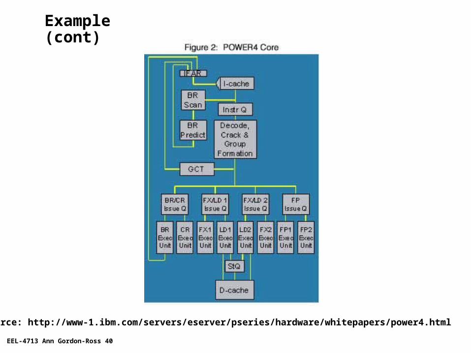
Example: IBM Power4
Source: http://www-1.ibm.com/servers/eserver/pseries/hardware/whitepapers/power4.html
EEL-4713 Ann Gordon-Ross 40
Example (cont)
Source: http://www-1.ibm.com/servers/eserver/pseries/hardware/whitepapers/power4.html

EEL-4713 Ann Gordon-Ross 41
Power4 cache hierarchy
° Level 1, on-chip
° Power-4 has two processors on a chip
• Each processor has its own L1 cache
• Each cache is split
° L1 Instruction Cache
• Direct mapped, 128-byte block managed as 4 32-byte sub-blocks
• 128 KB (64 KB per processor)
° L1 Data Cache
• 2-way, 128-byte block
• 64 KB (32 KB per processor)
° One 32-byte read or write per cycle

EEL-4713 Ann Gordon-Ross 42
Power4 cache hierarchy
° Level 2, on-chip
° Still SRAM
° Shared across two processors
° L2 configuration
• unified
• 8-way, 128-byte block
• 1.5 MB

EEL-4713 Ann Gordon-Ross 43
Power4 cache hierarchy
° Level 3, off-chip
• Directory tags for multiprocessing on-chip
° Embedded DRAM
° L3 configuration
• 8-way, 512-byte block managed as 4 128-byte sub-blocks
• 32 MB
• shared

EEL-4713 Ann Gordon-Ross 44
Power5 cache hierarchy
° Improvements in size, associativity to reduce capacity/conflict misses
° L1 I-cache: 2-way set associative
° L1 D-cache: 4-way set associative
° L2 unified cache: 1.92MB, 10-way associative, 13-cycle latency
° L3 unified cache: 36MB, 12-way associative, 87-cycle latency
° Memory: 220-cycle latency
° http://www.realworldtech.com/page.cfm?ArticleID=RWT100404214638&p=3

EEL-4713 Ann Gordon-Ross 45
Summary:
° The Principle of Locality:
• Programs access a relatively small portion of the address space at any instant of time.
- Temporal Locality: Locality in Time
- Spatial Locality: Locality in Space
° Three Major Categories of Cache Misses:
• Compulsory Misses: cold start misses.
• Conflict Misses: increase cache size and/or associativity.
• Capacity Misses: increase cache size
° Write Policy:
• Write Through: need a write buffer
• Write Back: control can be complex