ee457 quiz fall2018 - university of southern california
TRANSCRIPT

September 20, 2018 9:18 am EE457 Quiz - Fall 2018 C Copyright 2018 Gandhi Puvvada
EE457 Quiz (~10%)Closed-book Closed-notes Exam; No cheat sheets;
Ordinary calculators may be used but not the smart phone with calculators. Verilog Guides are not needed and are not allowed.Smart phones, tablets (and any kind of computing/Internet devices) are not allowed.
This is a Crowdmark exam. Please do not write on margins or on backside. Use HB or 1H pencil.
Fall 2018Instructor: Gandhi Puvvada
Thursday, 9/20/2018 (A 3-hour exam) 05:30 PM - 08:30 PM (180 min) in THH201Please do not write your student ID
Student’s DEN D2L username: @usc.edu
Viterbi School of Engineering, University of Southern California
Ques# Topic Page# Time Points Score
1 State Diagram, RTL Design 2-6 60 min. 99
2 Unsigned and Signed numbers 7-8 25 min. 48
3 CPU Performance 9-9 20 min. 28
4 MIPS processor ISA, Byte-addressable processors
10-10 20 min. 44
5 Single-Cycle CPU 11-12 25 min. 44
Total 1+11+1 150 min. 263
Perfect Score 250
September 20, 2018 8:55 am EE457 Quiz - Fall 2018 C Copyright 2018 Gandhi Puvvada
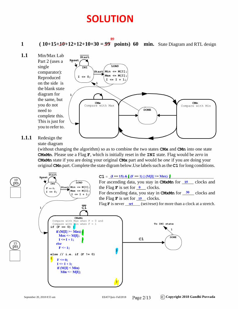
1 ( 10+15+10+12+12+10+30 = 99 points) 60 min. State Diagram and RTL design
1.1 Min/Max Lab Part 2 (uses a single comparator): Reproduced on the side is the blank state diagram for the same, but you do not need to complete this. This is just for you to refer to.
1.1.1 Redesign the state diagram (without changing the algorithm) so as to combine the two states CMx and CMn into one state CMxMn. Please use a Flag F, which is initially reset in the INI state. Flag would be zero in CMxMn state if you are doing your original CMx part and would be one if you are doing your original CMn part. Complete the state digram below.Use labels such as the C1 for long conditions.
ResetStart
Start
1
INI LOAD
DONE
CMx
I <= 0;
Min <= M[I];Max <= M[I];I <= I + 1;
CMn
1
Compare with Max Compare with Min
15pts
10pts
ResetStart
Start
1
INI LOAD
DONE
CMxMn
I <= 0;
Min <= M[I];Max <= M[I];I <= I + 1;
1
Compare with Max when F = 0 andCompare with Min when F = 1
F <= 0;
C1
C1
C1 = ______________________________________________________ For ascending data, you stay in CMxMn for _____ clocks andthe Flag F is set for ____ clocks.For descending data, you stay in CMxMn for _____ clocks andthe Flag F is set for ____ clocks. Flag F is never _______ (set/reset) for more than a clock at a stretch.
To INI stateif (F == 0) {
}else // i.e. if (F != 0) {
}
September 20, 2018 8:55 am EE457 Quiz - Fall 2018 C Copyright 2018 Gandhi Puvvada
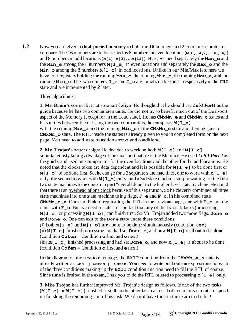
1.2 Now you are given a dual-ported memory to hold the 16 numbers and 2 comparison units to compare. The 16 numbers are to be treated as 8 numbers in even locations (M[0], M[2], ...M[14]) and 8 numbers in odd locations (M[1], M[3], ...M[15]). Here, we need separately the Max_e and the Min_e among the 8 numbers M[I_e] in even locations and separately the Max_o and the Min_o among the 8 numbers M[I_o] in odd locations. Unlike in our Min/Max lab, here we have four registers holding the running Max_e, the running Min_e, the running Max_o, and the running Min_o. The two counters, I_e and I_o are initialized to 0 and 1 respectively in the INI state and are incremented by 2 later.
Three algorithms:
1. Mr. Bruin’s correct but not so smart design: He thought that he should use Lab1 Part1 as the guide because he has two comparison units. He did not try to benefit much out of the Dual-port aspect of the Memory (except for in the Load state). He has CMxMn_e and CMxMn_o states and he shuttles between them. Using the two comparators, he compares M[I_e] with the running Max_e and the running Min_e in the CMxMn_e state and then he goes to CMxMn_o state. The RTL inside the states is already given to you in completed form on the next page. You need to add state transition arrows and conditions.
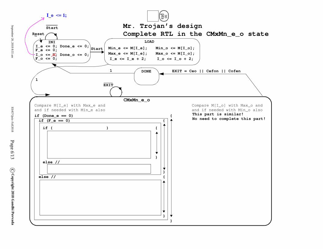
2. Mr. Trojan’s better design: He decided to work on both M[I_e] and M[I_o] simultaneously taking advantage of the dual-port nature of the Memory. He used Lab 1 Part 2 as the guide, and used one comparator for the even locations and the other for the odd locations. He noted that the clocks taken are data dependent and it is possible for M[I_e] to be done first or M[I_o] to be done first. So, he can go for a 3 separate state machines, one to work with M[I_e] only, the second to work with M[I_o] only, and a 3rd state machine simply waiting for the first two state machines to be done to report "overall done" to the higher-level state machine. He noted that there is an overhead of one clock because of this separation. So he cleverly combined all three state machines into one state machine using flags, F_e and F_o, in his combined state CMxMn_e_o. One can think of replicating the RTL in the previous page, one with F_e and the other with F_o. But we need to cater for the fact that any of the two sub-tasks (processing M[I_e] or processing M[I_o]) can finish first. So Mr. Trojan added two more flags, Done_e and Done_o. One can exit to the Done state under three conditions:(i) both M[I_e] and M[I_o] are about to be done simultaneously (condition Ceo)(ii) M[I_e] finished processing and had set Done_e, and now M[I_o] is about to be done (condition Cefon = Condition e first and o next)(iii) M[I_o] finished processing and had set Done_o, and now M[I_e] is about to be done (condition Cofen = Condition o first and e next)
In the diagram on the next to next page, the EXIT condition from the CMxMn_e_o state is already written as Ceo || Cefon || Cofen. You need to write out boolean expressions for each of the three conditions making up the EXIT condition and you need to fill the RTL of course.Since time is limited in the exam, I ask you to do the RTL related to processing M[I_e] only.
3. Miss Trojan has further improved Mr. Trojan’s design as follows. If one of the two tasks (M[I_e] or M[I_o]) finished first, then the other task can use both comparison units to speed up finishing the remaining part of his task. We do not have time in the exam to do this!

September 20, 2018 8:55 am
EE457 Quiz - Fall 2018
CC
opyright 2018 Gandhi Puvvada
12pts
Reset
Start
Start
1
INI LOAD
DONE
CMxMn_e
I_o <= 1;
Min_e <= M[I_e];Max_e <= M[I_e];I_e <= I_e + 2;
1
Compare M[I_e] with Max_e and Min_e
Min_o <= M[I_o];Max_o <= M[I_o];I_o <= I_o + 2;
I_e <= 0;
if (M[I_e] >= Max_e) Max_e <= M[I_e];
if (M[I_e] <= Min_e) Min_e <= M[I_e];
I_e <= I_e + 2;
CMxMn_oCompare M[I_o] with Max_o and Min_o
if (M[I_o] >= Max_o) Max_o <= M[I_o];
if (M[I_o] <= Min_o) Min_o <= M[I_o];
I_o <= I_o + 2;
Complete Mr. Bruin’s design here.RTL (insides the states) is already complete.
September 20, 2018 8:55 am EE457 Quiz - Fall 2018 C Copyright 2018 Gandhi Puvvada
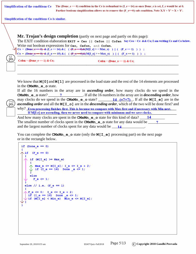
Mr. Trojan’s design completion (partly on next page and partly on this page):The EXIT condition elaboration EXIT = Ceo || Cefon || CofenWrite out boolean expressions for Ceo, Cefon, and Cofen.
____________________________________________________________________________________
____________________________________________________________________________________
____________________________________________________________________________________
We know that M[0]and M[1] are processed in the load state and the rest of the 14 elements are processedin the CMxMn_e_o state. If all the 16 numbers in the array are in ascending order, how many clocks do we spend in theCMxMn_e_o state? __________________. If all the 16 numbers in the array are in descending order, howmay clocks do we spend in the CMxMn_e_o state? __________________. If all the M[I_e] are in theascending order and all the M[I_o] are in the descending order, which of the two will be done first? andwhy? _________________________________________________________________________________________________________________________________________________________________And how many clocks are spent in the CMxMn_e_o state for this kind of data? _____________ The smallest number of clocks spent in the CMxMn_e_o state for any data would be ________________and the largest number of clocks spent for any data would be _________________.
You can complete the CMxMn_e_o state (only the M[I_e] processing part) on the next page or in the rectangle below.
12pts
7+3pts
September 20, 2018 8:55 am
EE457 Quiz - Fall 2018
CC
opyright 2018 Gandhi Puvvada
30pts
Reset
Start
Start
1
INI LOAD
DONE
CMxMn_e_o
Min_e <= M[I_e];Max_e <= M[I_e];I_e <= I_e + 2;
1
Compare M[I_e] with Max_e and
Min_o <= M[I_o];Max_o <= M[I_o];I_o <= I_o + 2;
I_e <= 0; Done_e <= 0;
and if needed with Min_e alsoCompare M[I_o] with Max_o and and if needed with Min_o also
if (Done_e == 0) {if (F_e == 0) {
if ( ) {
}else //
}else // {
} }
F_e <= 0;I_o <= 0; Done_o <= 0;F_o <= 0;
EXIT = Ceo || Cefon || Cofen
EXIT
This part is similar!No need to complete this part!
Mr. Trojan’s designComplete RTL in the CMxMn_e_o state
September 20, 2018 8:55 am EE457 Quiz - Fall 2018 C Copyright 2018 Gandhi Puvvada
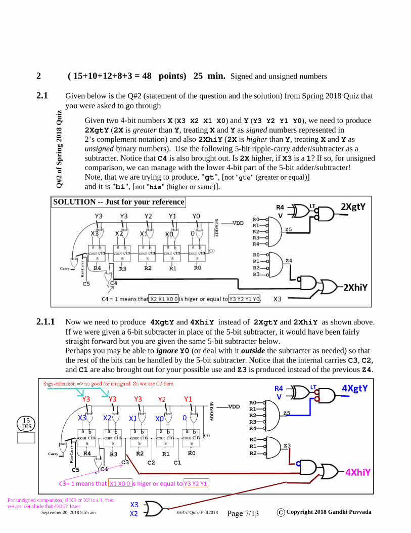
2 ( 15+10+12+8+3 = 48 points) 25 min. Signed and unsigned numbers
2.1 Given below is the Q#2 (statement of the question and the solution) from Spring 2018 Quiz that you were asked to go through
Given two 4-bit numbers X (X3 X2 X1 X0) and Y (Y3 Y2 Y1 Y0), we need to produce2XgtY (2X is greater than Y, treating X and Y as signed numbers represented in 2’s complement notation) and also 2XhiY (2X is higher than Y, treating X and Y asunsigned binary numbers). Use the following 5-bit ripple-carry adder/subtracter as asubtracter. Notice that C4 is also brought out. Is 2X higher, if X3 is a 1? If so, for unsignedcomparison, we can manage with the lower 4-bit part of the 5-bit adder/subtracter! Note, that we are trying to produce, "gt", [not "gte" (greater or equal)] and it is "hi", [not "his" (higher or same)].
2.1.1 Now we need to produce 4XgtY and 4XhiY instead of 2XgtY and 2XhiY as shown above.If we were given a 6-bit subtracter in place of the 5-bit subtracter, it would have been fairly straight forward but you are given the same 5-bit subtracter below. Perhaps you may be able to ignore Y0 (or deal with it outside the subtracter as needed) so that the rest of the bits can be handled by the 5-bit subtracter. Notice that the internal carries C3, C2, and C1 are also brought out for your possible use and Z3 is produced instead of the previous Z4.
SOLUTION -- Just for your reference
15 ptsa b
cins
cout C0
AD
D/S
UB
a bcin
scout
a bcin
scout
a bcin
scout
Raw
Car
ry
Carry
VC4C5
R4 R3 R2 R1 R0
VDD
R0R1R2
R0R1R2R3R4
Z5
Z3
C3 C2 C1
a bcin
scout
Q#2
of S
prin
g 20
18 Q
uiz
September 20, 2018 8:55 am EE457 Quiz - Fall 2018 C Copyright 2018 Gandhi Puvvada
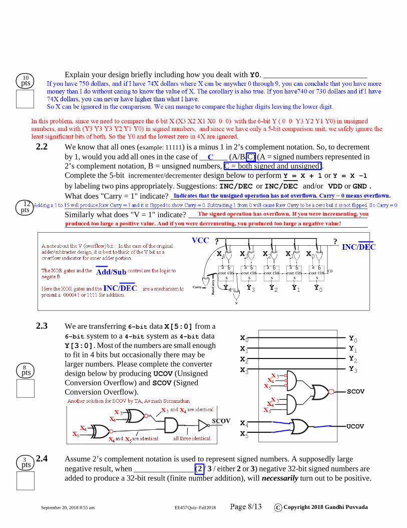
Explain your design briefly including how you dealt with Y0. __________________________ ____________________________________________________________________________ ____________________________________________________________________________ ____________________________________________________________________________ ____________________________________________________________________________ ____________________________________________________________________________
2.2 We know that all ones (example: 11111) is a minus 1 in 2’s complement notation. So, to decrement by 1, would you add all ones in the case of _______ (A/B/C) (A = signed numbers represented in 2’s complement notation, B = unsigned numbers, C = both signed and unsigned). Complete the 5-bit incrementer/decrementer design below to perform Y = X + 1 or Y = X -1 by labeling two pins appropriately. Suggestions: INC/DEC or INC/DEC and/or VDD or GND .What does "Carry = 1" indicate? ______________________________________________________________________________________________________________________________Similarly what does "V = 1" indicate? _________________________________________________________________________________________________________________________
2.3 We are transferring 6-bit data X[5:0] from a 6-bit system to a 4-bit system as 4-bit data Y[3:0]. Most of the numbers are small enough to fit in 4 bits but occasionally there may be larger numbers. Please complete the converter design below by producing UCOV (Unsigned Conversion Overflow) and SCOV (Signed Conversion Overflow).
2.4 Assume 2’s complement notation is used to represent signed numbers. A supposedly large negative result, when _______________ (2 / 3 / either 2 or 3) negative 32-bit signed numbers are added to produce a 32-bit result (finite number addition), will necessarily turn out to be positive.
10pts
pts12
a bcin
scout C0
a bcin
scout
a bcin
scout
a bcin
scout
a bcin
scout
Raw
Car
ry
Carry
V
? ?X4 X3 X2 X1 X0
Y4 Y3 Y2 Y1 Y0
X0X1X2X3
X4X5
Y3
Y0Y1Y2
UCOV
SCOV
8pts
Blank space below for rough work
3pts

September 20, 2018 8:55 am EE457 Quiz - Fall 2018 C Copyright 2018 Gandhi Puvvada
3 ( 8 + 10 + 10 = 28 points) 20 min. Performance:
There are four categories of instructions, A, B, C, and D, taking 3, 4, 5, and 6 clocks per instruction (CPI) respectively. Your colleague proposed to change resources in the datapath to improve performance of instructions in the A category by 1 clock even though this causes increase in the number of clocks taken by instructions in the D category by 3 clocks (without changing clock frequency). So, the new CPI of A, B, C, and D, will be 2, 4, 5, and 9. He argues that A is more frequently used compared to D, so overall this should be beneficial. Consider each of the following two questions separately and individually and arrive at its answer if adequate data is available. If data is inadequate, state what is missing to arrive at the needed answer.
3.1 If the frequency of occurrence of instructions of category D is 2% in the dynamic execution trace of a benchmark, what should be the minimum frequency of occurrence of instructions of category A you need before you can consider the proposed change to the datapath?__________________________________________________________________________________ __________________________________________________________________________________ __________________________________________________________________________________ __________________________________________________________________________________ __________________________________________________________________________________ ___________________________________________________________________________________
3.2 If the percentage of time spent executing instructions of category D is 2% in the dynamic execution trace of a benchmark, what should be the minimum percentage of time spent executing instructions of category A you need before you can consider the proposed change to the datapath?__________________________________________________________________________________ __________________________________________________________________________________ __________________________________________________________________________________ __________________________________________________________________________________ __________________________________________________________________________________ ___________________________________________________________________________________
3.3 The first fact implies the second fact. _________ (True / False). 1. "the frequency of occurrence of instructions of category D is 2% in the dynamic execution trace of a benchmark" 2. "the percentage of time spent executing instructions of category D is 2% in the dynamic execution trace of a benchmark".
The above two facts are inconsistent with each other; i.e. if one of them is right the other can not be true. __________ (True / False). Please provide quantitative support (some calculation, ...).____________________________________________________________________________________________________________________________________________________________________________________________________________________________________________________________________________________________________________________________________________________________________________________________
8pts
10pts
10pts

September 20, 2018 8:55 am EE457 Quiz - Fall 2018 C Copyright 2018 Gandhi Puvvada
4 ( 5 + 7 + 20 + 12 = 44 points) 20 min. MIPs Instructions and Memory addresses
4.1 The ______ (1/2/3) instruction(s) _______________ (preceding/following) the JAL instruction in execution (in execution = in the dynamic execution trace), together with the JAL instruction in MIPS make up the CISC CALL instruction. Similarly the ______ (1/2/3) instruction(s) _______________ (preceding/following) the JR $31 instruction in execution (in execution = in the dynamic execution trace), together with the JR $31 instruction in MIPS make up the CISC RTN (Return) instruction.
4.2 Intel follows ___________ (Little Endian / Big Endian) system. In the Intel 80486 processor system address space, byte 0000_800CH is the ____________ (most / least) significant byte of the 32-bit word with system address ______________ (state in hexadecimal).The 32-bit word 8000 consists of the four bytes 8000, 8001, 8002, and 8003 in ________________________________ (Little-Endian / Big-Endian / both kinds of /neither kind of) processor.
4.3 Intel processors, 80486 and i860, are both 32-bit logical address, byte addressable processors.The 80486 is a 32-bit data processor where as the i860 is a 64-bit data processor. Their address space(s) is/are ________ (the same / different). State the size of their address space(s): ____________________. If stacks of 4 MByte SRAM chips are placed in their byte-wide memory banks to fill-up their entire address spaces, what are the lowest and highest system byte addresses which map to the bottom and the top of the specific 4 MByte chip to which the system byte address 2345_ABC6 hex maps to?
In the case of 80486, the bottom is _ _ _ _ _ _ _ _ _ hex and the top is _ _ _ _ _ _ _ _ _ hex.
And in the case of i860, the bottom is _ _ _ _ _ _ _ _ _ hex and the top is _ _ _ _ _ _ _ _ _ hex.And if this chip goes bad, what is the total system address range in hex that needs to be declared as unusable?
(i) in the case of 80486 processor, it is _ _ _ _ _ _ _ _ _ hex to _ _ _ _ _ _ _ _ _ hex.
(ii) in the case of i860 processor, it is _ _ _ _ _ _ _ _ _ hex to _ _ _ _ _ _ _ _ _ hex.
4.3.1 Complete address decoding to generate Group-Selects (/GS_486 and /GS_860) for the row of chips and also show the rest of the labels for address, data, and byte-enable.
4+1pts
5+2pts
16+4 pts
12pts
A31A30A29A28
CS
WERD
A[ ]D[7:0]
D[ ]
A[ : ]
BE
4 MByte
2
/GS_486
A31A30A29A28
CS
WERD
A[ ]D[7:0]
D[ ]
A[ : ]
BE
4 MByte
2
/GS_860
Intel 80486 Intel i860
September 20, 2018 8:55 am EE457 Quiz - Fall 2018 C Copyright 2018 Gandhi Puvvada
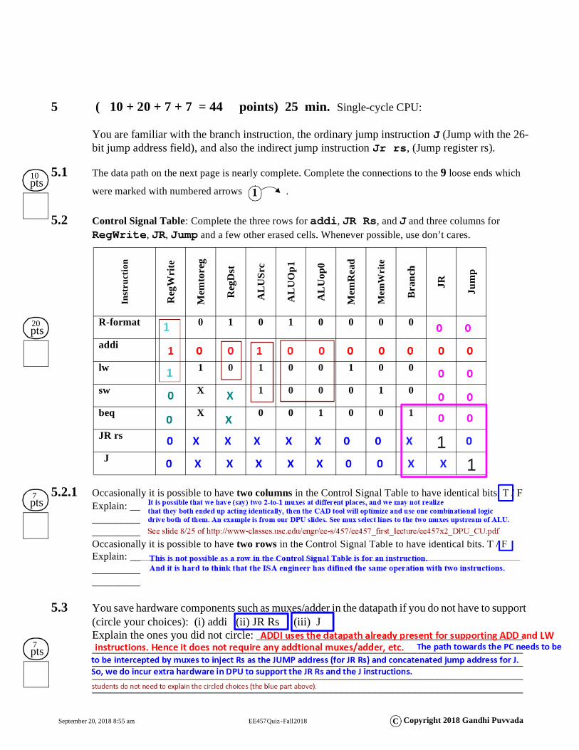
5 ( 10 + 20 + 7 + 7 = 44 points) 25 min. Single-cycle CPU:
You are familiar with the branch instruction, the ordinary jump instruction J (Jump with the 26-bit jump address field), and also the indirect jump instruction Jr rs, (Jump register rs).
5.1 The data path on the next page is nearly complete. Complete the connections to the 9 loose ends which
were marked with numbered arrows .
5.2 Control Signal Table: Complete the three rows for addi, JR Rs, and J and three columns for RegWrite, JR, Jump and a few other erased cells. Whenever possible, use don’t cares.
5.2.1 Occasionally it is possible to have two columns in the Control Signal Table to have identical bits. T / FExplain: __________________________________________________________________________________________________________________________________________________________________________________________________________________________________________Occasionally it is possible to have two rows in the Control Signal Table to have identical bits. T / FExplain: __________________________________________________________________________________________________________________________________________________________________________________________________________________________________________
5.3 You save hardware components such as muxes/adder in the datapath if you do not have to support (circle your choices): (i) addi (ii) JR Rs (iii) J Explain the ones you did not circle: _______________________________________________________________________________________________________________________________________________________________________________________________________________________________________________________________________________________________________________________________________________________________
Inst
ruct
ion
Reg
Wri
te
Mem
tore
g
Reg
Dst
AL
USr
c
AL
UO
p1
AL
Uop
0
Mem
Rea
d
Mem
Wri
te
Bra
nch
JR Jum
p
R-format 0 1 0 1 0 0 0 0
addi
lw 1 0 1 0 0 1 0 0
sw X 1 0 0 0 1 0
beq X 0 0 1 0 0 1
JR rs 1 J 1
10pts
1
20pts
7pts
7pts

Control
JumpJR PCSrc
RegDst
BranchMemReadMemtoReg
ALUOpMemWrite
ALUSrcRegWrite
Zero
ALUcontrol
1
0
1
0
JR Jump
6
Jump Address [31:0]Instruction [31:0]
PC+4 [31:28]
21 3 4 5
7
89
September 20, 2018 8:55 am EE457 Quiz - Fall 2018 C Copyright 2018 Gandhi Puvvada
Blank page: Please write your name and email. Tear it off and use for rough work. Do not submit at the end.
Student’s Last Name:____________________ email: __________________
It is not difficult to get an A in EE457. You need to work for it and seek help from the 457 teaching team on whatever you do not understand. We are eager to help you. The next four topics, Multi-cycle CPU, pipelined CPU, cache and virtual memory are interesting and challenging too. They are the focus of the midterm exam. Then we cover advanced topics. Best! Gandhi, TAs: Pravin, and Avinash, Mentors: Smrthi, Gaurav, and Sid HW Graders: Yen-Po, Tanvir, and Nishant Lab graders: Yongzen, Aeshaani, and Sukriti