ee457 final exam (~30% to 36%) - university of southern
TRANSCRIPT

May 9, 2018 8:49 am EE457 Final - Spring 2018 1 / 13 C Copyright 2018 Gandhi Puvvada
EE457 Final Exam (~30% to 36%)Closed-book Closed-notes Exam; No cheat sheets;
Ordinary calculators may be used but not the smart phone with calculators. Verilog Guides are not needed and are not allowed.Smart phones, tablets (and any kind of computing/Internet devices) are not allowed.
This is a Crowdmark exam. Please do not write on margins or on backside.
Spring 2018Instructor: Gandhi Puvvada
Wednesday, 5/9/2018 (A 3-hour exam) 04:30 PM - 07:30 PM (180 min) in SGM124Please do not write your student ID
Ques# Topic Page# Time Points Score
1 Tomasulo 2-5 50 min 91
2 Arithmetic 6 20 min 52
3 Virtual Memory 7 20 min 34
4 Cache 8 8 min 15
5 Miscellaneous advanced topics 8-9 30 min 70
6 Lab 6 Early Branch, EX and MEM stages merged
10-12 40 min 80
Total Cover+11+ Blank = 13
168 min. 342
Perfect Score 330

May 9, 2018 8:49 am EE457 Final - Spring 2018 2 / 13 C Copyright 2018 Gandhi Puvvada
1 ( 18+4+2+16+10+10+4+7.5+3.5+6+1 = 91 points) 50 min. Tomasulo
I-Cache
Register Status Table
Integer / Branch
D-CacheDiv Mul
TAG FIFO
Instruc. Queue
Reg
. File
Int.
Que
ue
L/S
Que
ue
Div
Que
ue
Mul
t. Q
ueue
CDB
Issue Unit
Dispatch
Load Buffer
IoI-OoW-OoC with RST
IoI-OoE-IoC_with_ROB
I-Cache
Br. Pred. Buffer
lw mult
Integer / Branch Div Mul
ROB
InstructionPrefetch Queue
Reg
. File
Int.
Que
ue
L/S
Que
ue
Div
Que
ue
Mul
t. Q
ueue
CDB
Issue Unit
D-Cache
Dispatch
1 mult2 Completed3 lw4 Completed
StoreAddr. Buffer D-Cache
L/S Buffer
Current Head
Current TailWP
Addr.Adder
No store buffer
for EE457
Stores hit in cache
always for EE457

May 9, 2018 8:49 am EE457 Final - Spring 2018 3 / 13 C Copyright 2018 Gandhi Puvvada
You know the above two designs very well. The top is the OoC design and bottom is the IoC design.
1.1 OoC design components: RF, RST, and TAG FIFO
1.2 Between the Data Cache and the CDB, it is Load Buffer in the case of the OoC and LS Buffer in the case of the IoC. Explain: _____________________________________________________________________________________________________________________________________________________________________________
1.3 Exceptions can be supported in the ________ (OoC/IoC/both) designs.
1.4 We said a few times,"we wish we could "UNDO" like in word processing, and get back to LION
in $8 from the current value of ANT in the above diagram of RST".Explain the context and discuss. Is this needed in the OoC design or the IoC design?
18 pts $0$1$2
$8
$31
$0$1$2
$8
$31
RST RF
LION TIGER CAT ANT
ANT
In our Summer 2008 EE560 project of the OoC design, we had a RST of 32x7, a RFof 32x32 and a Tag FIFO of 64x6. Some choices may be random but not all of them.Are there any relations between these sizes (depths and widths)? Is there a valid bit in any of these? Who performs an associative search on whom and when? How many of what size comparators are involved in that associative search?In your analysis, consider scaling this to a new bigger OoC design for a 64-bit processor with a RF of 64 x 64 and a 128 deep TAG FIFO.
0 1 2
63
TAG FIFO
DOG
Current design: RST of 32x7 , a RF of 32x32 and a Tag FIFO of 64x6 Scaled up design: RST of ____ , a RF of 64x64 and a Tag FIFO of 128x___
D_Cache
Load Buffer
D_Cache
LS Buffer 4 pts
2 pts
LION TIGER CAT ANT$8 ANT
16 pts

May 9, 2018 8:49 am EE457 Final - Spring 2018 4 / 13 C Copyright 2018 Gandhi Puvvada
1.5 In the case of Tomasulo #3 (the more current IoC design of EE560, introduced in the last lecture), _________ (FRAT / RRAT) avoids the expensive associative prioritized search in ROB (by holding the latest mapping between each architectural register and the locations in the physical register file). FRAT stands for Front-end RAT (Register Alias Table) associated with the dispatch process, where as RRAT stands for the ________ RAT. In case of branch misprediction, ______ (FRAT / RRAT) needs to be reverted to its state before the dispatch of the mispredicted branch. We take snap shots (check-points) of the ______ (FRAT / RRAT) and store them. Check-points are taken for _________________ (low-confidence/high-confidence) branches so if it fails, we restore ______ (FRAT / RRAT) by copying the checkpoint to it. But if a _______ _____________ (low-confidence / high-confidence) branch (for whom we did not create a check-point) got mispredicted, we jump to the nearest check-point and then walk though the ROB by rewinding/fast-forwarding the ______________ (dispatch / graduation) process to the mispredicted branch. This is similar to a _______ (DVD /VHS tape) where we jump to the nearest chapter point and then rewind or fast forward to the scene of interest.
1.6 Initially (on power-on), a FIFO between a producer and a consumer is _______ (empty/full).ROB in the IoC design is initially _______ (empty/full). TAG FIFO in the OoC design is initially _______ (empty/full). Do you use full or empty to describe the state of the RST anytime? Y / NDo you use the word FULL for a direct-mapped cache? How about Fully Associative TLB? ____________________________________________________________________________________________________________________________________________________________________________________________________________________________________________________________________________________________________________
1.7 RAS (Return Address Stack) _______ (is / is not) used in the OoC design because __________________________________________________________________________________________________________________________________________________________________
1.8 You use TOSP+1 to _________ (push /pop) return address.You use TOSP to _________ (push /pop) return address.If recursive routines are very rarely used, (i) would you still make the RAS a circular stack? _____ (Y / N), (ii) can you remove the UseWhenEmpty register? _____ (Y / N). Since the RAS holds return addresses, what is the width of this stack array? ________.
1.9 The branch prediction in the IoC design is considered equivalent to predicting from the ________ (IF stage / ID stage) because ________________________________________________________________________________________________________________________________
1.10 If ROB is full in the clock when a branch on CDB announces that it was mispredicted, (circle all applicable)i) WP and RP must be pointing to the same location in the ROBii) The branch instruction can potentially be the junior-most instruction in the ROB, pointed to by _________ (RP, RP-1, RP+1, WP, WP-1, WP+1)iii) The branch instruction can potentially be the senior-most instruction in the ROB, pointed to by _________ (RP, RP-1, RP+1, WP, WP-1, WP+1)
10 pts
10 pts
4 pts
TOSPTOSP+1
0123
RAS
UseWhenEmpty
7.5 pts
3.5 pts
6 pts
May 9, 2018 8:49 am EE457 Final - Spring 2018 5 / 13 C Copyright 2018 Gandhi Puvvada
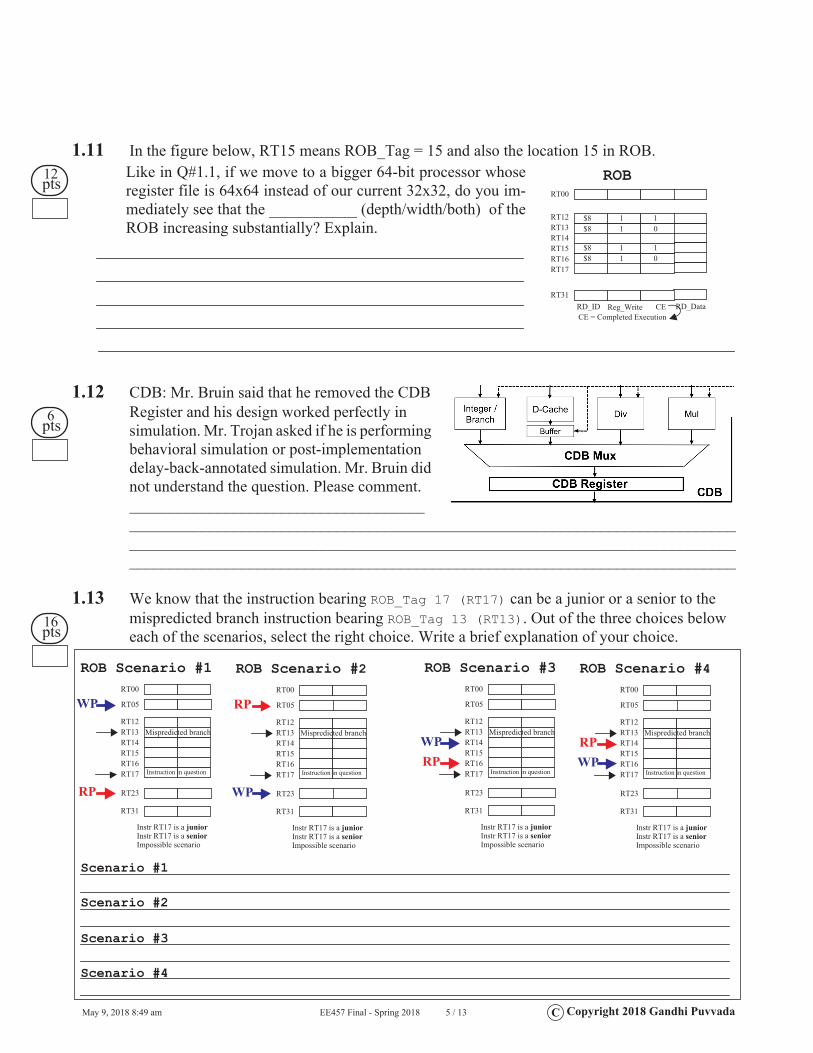
1.11 In the figure below, RT15 means ROB_Tag = 15 and also the location 15 in ROB.
1.12 CDB: Mr. Bruin said that he removed the CDB Register and his design worked perfectly in simulation. Mr. Trojan asked if he is performing behavioral simulation or post-implementation delay-back-annotated simulation. Mr. Bruin did not understand the question. Please comment._________________________________________________________________________________________________________________________________________________________________________________________________________________________________________________________________________
1.13 We know that the instruction bearing ROB_Tag 17 (RT17) can be a junior or a senior to the mispredicted branch instruction bearing ROB_Tag 13 (RT13). Out of the three choices below each of the scenarios, select the right choice. Write a brief explanation of your choice.
12 pts
RD_Data
Like in Q#1.1, if we move to a bigger 64-bit processor whoseregister file is 64x64 instead of our current 32x32, do you im-mediately see that the ___________ (depth/width/both) of theROB increasing substantially? Explain.
ROB
$8RT12RT13RT14RT15
RD_ID Reg_Write CE
RT00
RT31
CE = Completed Execution
1 1$8 1 0
$8 1 0RT16RT17
$8 1 1
6 pts
16 pts
ROB Scenario #1
RT12RT13RT14RT15
RT00
RT31
RT16RT17
RT23
RT05
Mispredicted branch
Instruction in question
Instr RT17 is a juniorInstr RT17 is a seniorImpossible scenario
WP
RP
ROB Scenario #2
RT12RT13RT14RT15
RT00
RT31
RT16RT17
RT23
RT05
Mispredicted branch
Instruction in question
Instr RT17 is a juniorInstr RT17 is a seniorImpossible scenario
RP
WP
ROB Scenario #3
RT12RT13RT14RT15
RT00
RT31
RT16RT17
RT23
RT05
Mispredicted branch
Instruction in question
Instr RT17 is a juniorInstr RT17 is a seniorImpossible scenario
WPRP
ROB Scenario #4
RT12RT13RT14RT15
RT00
RT31
RT16RT17
RT23
RT05
Mispredicted branch
Instruction in question
Instr RT17 is a juniorInstr RT17 is a seniorImpossible scenario
RPWP
Scenario #1
Scenario #2
Scenario #3
Scenario #4

May 9, 2018 8:49 am EE457 Final - Spring 2018 6 / 13 C Copyright 2018 Gandhi Puvvada
2 ( 12+12+12+16 = 52 points) 20 min. Arithmetic (based on Lab 3 SLT, SLTU and Spring 2012 and Fall 2012 questions)
2.1 We are give two 4-bit subtracters with C3, C4 and R3 brought out as shown on the side.
On the upper-part, treat X and Y as unsigned numbers, and produce XhsY (X higher or same as Y) (opposite of Less Than Unsigned (SLTU) of Lab 3).
On the lower-part, treat X and Y as signed numbers, and produce XgeY (X greater or equal as Y) (opposite of Less Than Signed (SLT) of Lab 3).
2.2 Based on the Fall 2012 question on overflows:Treating X, Y and R as signed numbers,produce R = 0-X-Y (i.e. zero minus X minus Y) using two subtracters. Also produce overall overflow.
2.3 Unsigned series of additions and subtractions: R = A+B-C+D-EIn the above expression there are equal number of additions and subtractions. Hence there are _________ (equal/unequal) number of opportunities to overflow and underflow, which can potentially cancel each other. You are given two half- adders and a 2-bit comparator to complete the design and produce RR (Result_Right) signal.Does it matter we do the additions and subtractions alternatively? Y / N
4 invertersA
B
Adde
r
Cout
S
C4
Cin
Cout_1
C3
RY
X
?
R3
4 invertersA
B
Adde
r
Cout
S
C4
Cin
Cout_1
C3R
Y
X
?
R3
XhsY
XgeY
Unsigned
Signed
12 pts
12 pts
4 invertersA
B
Adde
r
Cout
S
C4
Cin
Cout_1
C3
IRX
0
?
IR3 4 inverters
A
B
Adde
r
Cout
S
C4Cin
Cout_1C3
RY
IR
?
R3
IR = Intermediate Result
Signed
12 pts
A
BS
Cin
Cout
4 inv
A
BS
Cin
Cout
A
BS
Cin
Cout
4 inv
A
BS
Cin
Cout
R
Adder
Adder
Adder
Adder
O1 O2
U1 U2
Unsigned
? ? ? ?
16 pts

May 9, 2018 8:49 am EE457 Final - Spring 2018 7 / 13 C Copyright 2018 Gandhi Puvvada
3 ( 8+8+18 = 34 points) 20 min. Virtual Memory:
In a system with 32-bit Virtual Address VA[31:0] and 32-bit physical address PA[31:0], the TLB uses set associative mapping with 256 sets, each set with 5 entries (Degree of associativity = 5). The PPFN is 5 hex digits long and has values in the rang 00000 hex to FFFFF hex. The same range applies to VPN also which is divided into 2 hex digits of Set field and 3 hex digits of TAG field. Divide the Virtual address and physical address below as appropriate.
Size of Virtual Page (in Kilobytes): _________________. Size of Physical Page Frame (in Kilobytes): ____________________.
When the TLB is full, is it possible to have (A) repetitions of Virtual TAGs in the 5 locations of any row (say the top-most row) Yes / No(B) repetitions of Virtual TAGs across rows (say in the first left-most column of 256 TAGs) Yes / No(C) repetitions of PPFNs in the 5 locations of any row (say the top-most row) Yes / No (D) repetitions of PPFNs across rows (say in the first left-most column of 256 PPFNs) Yes / No
Currently the TLB has only three entries as indicated by the three valid bits shown above. Fill-inthe three entries with Virtual TAGs and PPFNs of your choice in such a way that (a) the three virtual pages are as close to each other as possible (preferably adjacent to each other, if possible) and (b) the three physical page frames are also as close to each other as possible (preferably adjacent to each other, if possible). Write down the 3 + 3 = 6 page numbers in hex below.
VA31 VA[1:0] PA31 PA[1:0]8 pts
8 pts
The three VPNs inincrementing order:_____________________________________________
The three PPFNs inincrementing order:_____________________________________________
18 pts

May 9, 2018 8:49 am EE457 Final - Spring 2018 8 / 13 C Copyright 2018 Gandhi Puvvada
4 ( 15 points) 8 min. Cache
Consider a 160KB cache in a 32-bit physical address 64-bit data byte addressable system, block size = 4 64-bit words, set associative mapping, degree of set associativity = 5Complete the details of one TAG RAM and one Data RAM and state how many such items.
5 ( 6+3+9+4+4+8+8+4+3+12+6+3 = 70 points) 30 min. Miscellaneous advanced topics
5.1 The ideal CPI (clocks per instruction) of our OoO processor (IoI-OoE-IoC) is __________.The ideal CPI (clocks per instruction) of a simple 5-stage pipeline (IoI-IoE-IoC) is ______.The ideal CPI (clocks per instruction) of a 2-way Super-scalar machine is _____________.The ideal CPI (clocks per instruction) of a super-pipelined 10-stage (IoI-IoE-IoC) is ______.The ideal CPI (clocks per instruction) of a 4-threaded single core machine is ___________.The ideal CPI (clocks per instruction) of a 1-threaded 4-core machine is ______________.
5.2 Branch direction prediction becomes more important in __________ (deeper / shallow) pipelines.Branch direction prediction becomes more important in _____________ (out-of-order / in-order) executing pipelines.
5.3 In a 2-bit branch direction predictor, the four states on the right are for ______ (A / B) (A = the whole 1K-deep BPB, B = for each entry of the 1024 entries in the 1K-deep BPB). In implementation the two bits in an entry are either incremented or decremented, ________________________________ (at most one entry in one clock, one entry in every clock, all entries in one clock). Hence we need ___________________________________________ (just one incrementer/decrementer unit / 1024 incrementer/decrementer units). State change is done when a branch ____________________________________ (is predicted / reaches CDB and announces predicted right or mispredicted. SN to N state transition takes place when the branch is __________________(predicted right / mispredicted). N to SN state transition takes place when the branch is __________________(predicted right / mispredicted).
5.4 In the MPI (Miss rate per instruction) calculations, the “per instruction” refers to ___________ (all / only memory accessing) instructions. This facilitates quickly figure out the impact of the misses on _____________ (write the metric we calculated using this).
15 pts
A19 A18 A17 A16A31 A30 A29 A28 A27 A26 A25 A24 A23 A22 A21 A20 A3 A2 A1 A0A15 A14 A13 A12 A11 A10 A9 A8 A7 A6 A5 A4
(Byte enables)
(CPU address bits)
D[7
:0]
D[1
5:8]
D[2
3:16
]
D[3
1:24
]
DATA RAM( ___ more like this)
Address
Data_in
Data_out
1Valid Com
p un
it __
- bi
ts w
ide
Hit/Miss
( ___ more like this)TAG RAM with Comp. unit
1
Size
of o
neB
yte-
wid
e B
ank
____
_ x
8
/BE[7:0] 8
D[3
9:32
]
D[4
7:40
]
D[5
5:48
]
D[6
3:56
]
(CPU address bits)
(CPU address bits)
TAG RAM size: ____ x ____
6 pts
3 pts
SN N T ST
9 pts
4 pts
May 9, 2018 8:49 am EE457 Final - Spring 2018 9 / 13 C Copyright 2018 Gandhi Puvvada
5.5 Mutual Exclusion using atomic instruction pair like the LL and SC is needed in (circle all right answers)(i) single-core multi-threaded CPU (ii) multi-core multi-threaded CPU (iii) multi-core single-threaded CPU (iv) single-core single-threaded CPU but executing multiple interacting processes in a time-shared fashion.
5.6 CMT: In a 4-threaded core, circle the common resources below:PC, IFQ (Instr. Fetch Queue), I-TLB, I-cache, RF (Register file), TS (Thread Selection), IEU (Integer Execution Unit), FPU (Floating-point Execution unit), SB (Store Buffer), D-TLB, D-cache, SCU (Snoopy Control Unit for Cache Coherency)
5.7 Non-blocking caches _____________ (reduce/increase) processor stalls due to cache misses. They buffer the misses and ___________ (continue/wait) to serve other access requests from _____________ (same thread/different threads). MSHR, standing for ________________________________, buffers the missed cache access until it is served. Non-blocking cache is helpful in _______________________________ (instruction cache only/data cache only/both). Non-blocking caches have two controllers, such as CCU and SCU, so that one attends to the new requests while the other attends to the misses. T / F
5.8 Intel HTT stands for H_________ T___________ T___________ . Its generic name is ____ (A/B/C) where A = fine-grain multi-threading where all instructions dispatched in a clock are of the same thread but threads are switched on every clock, B = coarse-grain multi-threading where all instructions dispatched in a clock are of the same thread but threads are suspended for a cause such as cache miss, C = Simultaneous multi-threading where instructions dispatched in a clock can be any mix of the threads.
5.9 If you want to use one mega Data TLB instead of 4 individual TLBs for the 4 threads in a 4-threaded core, you will add to the entries of the TLB ______ (A / B). A = 2-bit thread ID , B = ASN (address space number = Process ID)
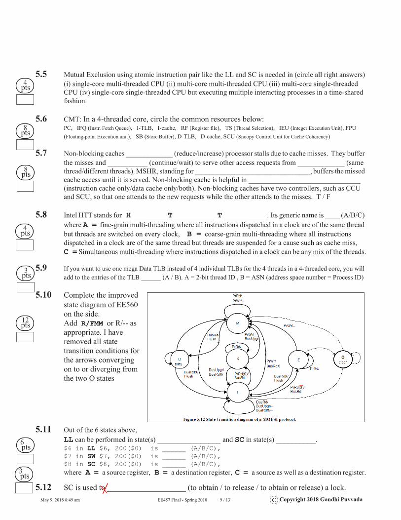
5.10 Complete the improved state diagram of EE560 on the side. Add R/FMM or R/-- as appropriate. I have removed all state transition conditions for the arrows converging on to or diverging from the two O states
5.11 Out of the 6 states above, LL can be performed in state(s) ________________ and SC in state(s) __________.$6 in LL $6, 200($0) is ______ (A/B/C), $7 in SW $7, 200($0) is ______ (A/B/C), $8 in SC $8, 200($0) is ______ (A/B/C), where A = a source register, B = a destination register, C = a source as well as a destination register.
5.12 SC is used to ____________________ (to obtain / to release / to obtain or release) a lock.
4 pts
8 pts
8 pts
4 pts
3 pts
12 pts
6 pts
3 pts

May 9, 2018 8:49 am EE457 Final - Spring 2018 10 / 13 C Copyright 2018 Gandhi Puvvada
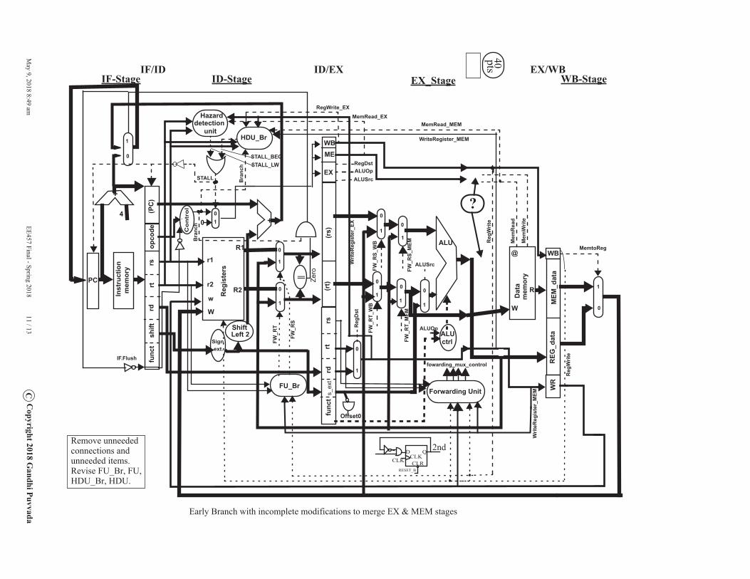
6 ( 40 + 40 = 80 points) 40 min. Lab 6 Early Branch Design -- EX and MEM stages combined:
Nothing needs to be done on this page. Complete your design on the next two pages. On the next page, I have mainly removed the EX/MEM stage register. Remove unneeded connections and unneeded items of the original 5-stage pipeline on the next page. Revise FU_Br, FU, HDU_Br, HDU as needed. On the further next page, complete the new EX stage stalling, Memory address, MR and MW.
Consider the left two instructions and compare them with the right two instructions.
lw $8, 0($2); lw $8, 40($2);sw $8, 0($2); sw $8, 60($2);
Let us say, for the sake of this problem, that we observed that many programs use lw and sw instructions with 0 offset (for their address calculation) as shown on the left quite often.
So we proposed to merge the EX and MEM stages into one stage called new EX. Now lw $8, 0($2) on the left side bypasses the ALU, and uses the raw $rs ($2 here) as the memory address. So the left-hand instructions require only 1 clock in the new EX stage. Hence instructions dependent on lw $8, 0($2) do not need to stall for one clock. This is a gain.
But instruction on the right need two clocks in the new EX stage for the address calculation to complete before you access memory. This is a loss. We use our standard mechanism of stalling a stage for exactly one clock (from our Lab 7 Part 3 SP2) to provide an extra clock for the right side instructions in the new EX stage.
Certainly, in the case of sw $8, 60($2), we should not convey MemWrite control signal in the first clock of the two clock process to the Data Memory before the address 60($2) is fully calculated by the ALU. Otherwise you would be corrupting the Data Memory. It is also important in the case of lw $8, 40($2), not to convey MemRead control signal in the first clock to avoid unwanted side-effects in the Data Cache. Make sure that the MR and MW are inactivate at all other times (other than the needed times).
We should convey the right (proper) address to the memory. We convey either the contents of Rs bypassing the ALU or the effective address as calculated by the ALU. Hence a mux is added in the address path of the Memory.
Offset0
D QCLKCLRCLK
RESET_B
2nd
EX
MEWB
ALUSrcALUOpRegDst
MemReadMemWrite
EN
Offset0SW_LW_0
SW_LW_N0
MR
MW
Offset is 0
Offset is not 0
I0[0]
I0[1]
I1[0]
I1[1]
Y[0]
Y[1]
S
ALU
ALUSrc
Dat
am
emor
y
@
W
R
1
0
1
0
May 9, 2018 8:49 am
EE457 Final - Spring 2018 11 / 13C
Copyright 2018 G
andhi Puvvada
Hazarddetection
unit
04
Inst
ruct
ion
mem
ory
PC
+
r1
r2
R1
R2w
W
opco
ders
rtrd
shift
func
t
Reg
iste
rs
Co
ntr
ol(PC
)
(rs)
(rt)
ALU
rtrd
ALUctrlSign
ext.
EX
MEWB
ALUSrcALUOpRegDst
ALUSrc
Reg
Dst
ALUOp
RegWrite_EX
Dat
am
emor
y
@
W
R
Mem
Rea
d
Mem
Writ
e
Reg
Writ
e
IF.Flush
WR
WB
MEM
_dat
aR
EG_d
ata
Reg
Writ
e
MemtoReg
+
=
func
ts_ext
ShiftLeft 2
Zero
Forwarding Unit
Early Branch with incomplete modifications to merge EX & MEM stages
IF/IDIF-Stage
ID/EXID-Stage EX_Stage
EX/WBWB-Stage
rs
MemRead_EXMemRead_MEM
Writ
eReg
iste
r_EX
FU_BrFW
_RS_
WB
FW_R
S_M
EM
FW_R
T_W
B
FW_R
T_M
EM
FW_R
T
FW_R
S
Writ
eReg
iste
r_M
EM
WriteRegister_MEMHDU_Br
STALL_BEQSTALL_LW
STALL
Bra
nch
01
0
1
1
0
0
1
11
11
1
00
00
0
0
0
1
Bra
nch
1
fowarding_mux_control
?
Offset0
D QCLKCLRCLK
RESET_B
2ndRemove unneeded connections and unneeded items. Revise FU_Br, FU,HDU_Br, HDU.
40 pts

May 9, 2018 8:49 am
EE457 Final - Spring 2018 12 / 13C
Copyright 2018 G
andhi Puvvada
04
Inst
ruct
ion
mem
ory
PC
+
r1
r2
R1
R2w
W
opco
ders
rtrd
shift
func
t
Reg
iste
rs
Co
ntr
ol(PC
)
(rs)
(rt)
ALU
rtrd
Signext.
EX
MEWB
ALUSrcALUOpRegDst
ALUSrc
Reg
Dst
Dat
am
emor
y
@
W
R
MemReadMemWrite
IF.Flush
WR
WB
MEM
_dat
aR
EG_d
ata
Reg
Writ
e
MemtoReg
+
=
func
ts_ext
ShiftLeft 2
Zero
Early Branch with incomplete modifications to merge EX & MEM stages
IF/IDIF-Stage
ID/EXID-Stage EX_Stage
EX/WBWB-Stage
rs
Bra
nch
01
0
1
1
0
0
0
1
1
Offset is 0
D QCLKCLRCLK
RESET_B
2nd
STALL
EN
EN
RESET_B
RESET_B
RESET_B
RESET_B
Offset0SW_LW_0
SW_LW_N0
MR
MW
Offset is 0
Offset is not 0
I0[0]
I0[1]
I1[0]
I1[1]
Y[0]
Y[1]
S
1
0
Complete the rest of the design.New EX stage stalling, Memory address, MR, MW.
40 pts

May 9, 2018 8:49 am EE457 Final - Spring 2018 13 / 13 C Copyright 2018 Gandhi Puvvada
Blank page: Please write your name and email. Tear it off and use it for rough work. Do not submit.Student’s Last Name:____________________ email: __________________
We enjoyed teaching this course! Hope you liked it! Hope to see some of you in EE560. Grades will be out in a week. Enjoy your summer break! Happy Holidays!!! Gandhi, TAs: Fangzhou, Chao, Mentors: Rui, Pravin HW Graders: Navtej, Rupam Lab graders: Ujwala, Aashish