Signal Generator Based on Direct Digital Synthesis Techniques Tao Wang,
International Journal of Digital Content Technology and its Applications. Volume 5, Number 8, August 2011
Signal Generator Based on Direct Digital Synthesis Techniques
Tao Wang, Taizhou University, [email protected]
doi:10.4156/jdcta.vol5.issue8.4
Abstract This paper describes a design of signal generator based on direct digital synthesis technique (DDS).
According to the basic principles of DDS using Matlab/DSP Builder establish DDS model, then compiling by the SignalCompiler tools and generating VHDL code. Finally download the relevant documents to the field programmable gate array (FPGA) chip EP2C5Q208C8N. EP2C5Q208C8N and digital-analog chip DAC908, high-speed operational amplifier THS4001 together to complete the signal generator’s hardware design. The system can output sine wave, square wave, triangle wave, phase shift keying (PSK), amplitude shift keying (ASK) and frequency shift keying (FSK). It’s stable, reliable and fairly practical.
Keywords: Matlab/DSP Builder, FPGA, DDS, Signal Generator
1. Introduction
DDS is a new frequency synthesis technology of using digital technology. It is by controlling the frequency, phase incremental step generate signals of different frequencies. It has a high frequency resolution, fast frequency switching can be achieved, and keep the continuum of phase when switching so as to realize the NC adjustment of frequency, phase and amplitude easily. Thus, in the frequency source of modern electronic systems and equipment, especially in communications, DDS has been widely applied. Currently we can use a dedicated chip or programmable logic chip to realize DDS. The function of specific DDS chip is more, but the control method is fixed, so it can not meet a variety of needs in reality. We can realize FM, phase modulation and amplitude modulation function easily by using of programmable logic chip, with good usability and flexibility. But the programming is more complex, and therefore not a good application. In this paper, model by Matlab/DSP Builder, and then very easy to implement the design of DDS signal generator in the FPGA, it avoid the complexity of programming and design DDS signal generator become very simple and quick. 2. Structure and principle of DDS
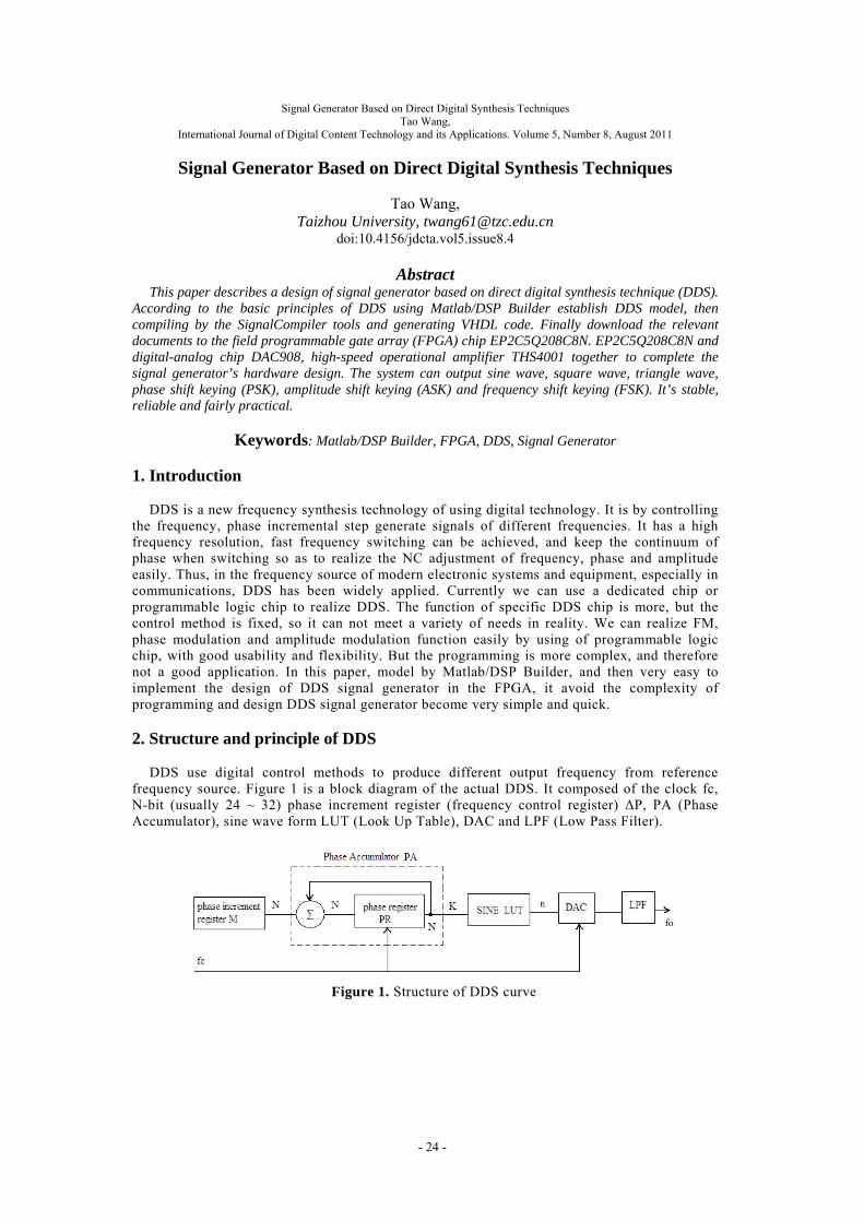
DDS use digital control methods to produce different output frequency from reference frequency source. Figure 1 is a block diagram of the actual DDS. It composed of the clock fc, N-bit (usually 24 ~ 32) phase increment register (frequency control register) ΔP, PA (Phase Accumulator), sine wave form LUT (Look Up Table), DAC and LPF (Low Pass Filter).
Figure 1. Structure of DDS curve
- 24 -
Signal Generator Based on Direct Digital Synthesis Techniques Tao Wang,
International Journal of Digital Content Technology and its Applications. Volume 5, Number 8, August 2011
A complete cycle of sine wave amplitude values is stored in LUT. In each clock cycle, the M
of ΔP and the PA to make a cumulative operation, the high-K-bit of sum work as LUT address, read waveform amplitude data from the LUT and sent to DAC, and output frequency fo through LPF. From this we can know change in ΔP can change the output frequency. Output frequency:
fo=M × fc/2n (1)
Frequency resolution:
fr = fc/2n (2) 3. The hardware design of signal source system
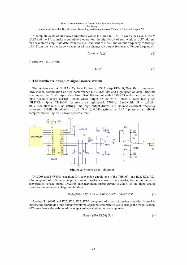
The system uses ALTERA's Cyclone II family FPGA chip EP2C5Q208C8N to implement DDS model, combination of high-performance DAC DAC908 and high-speed op amp THS4001 to complete the final output waveform. DAC908 output with 165MSPS update rate; no signal false dynamic range (SFDR): 68db when output 5MHz with 100MSPS rate; low glitch (GLITCH): 3pv/s. THS4001 features ultra high-speed: 270Mhz Bandwidth (G = 1,-3dB); 400V/usec slew rate, 40ns settling time; high output drive: Io = 100mA; excellent frequency parameter: 60MHz Bandwidth (0.1dB, G = 1), 0.04% gain error, 0.15 ° phase error; reliable complex model. Figure 2 shows system circuit.
Bit11
Bit22
Bit33
Bit44
Bit55
Bit66
Bit77
Bit88
Bit99
Bit1010
Bit1111
Bit1212
Bit1313
Bit1414
PD15
/INT_EXT16REF17
FSA18BW19
AGND20Iout221
Iout1 22BYP
23+VA 24
NC25
DGND 26+VD
27CLK28
U4
DAC908
3
26
47
U5
THS4001 3
26
47
U6
THS4001
C8
C5C7 C6
C9R18
C10C12
C13C11R19
R24
R26
2kR27
VCC_3.3V
-VCC-VCC
+VCC+VCC
12
J11
Fo
12
J10
R23R20
R21
R22
R17
R25
RW2
CLK
EP2C5Q208C8N
U3
Figure 2. System circuit diagram
DAC908 and THS4001 constitute DA conversion circuit, one of the THS4001 and R21, R22, R23,
R24 composed of differential amplifier circuit, bipolar is converted to unipolar, the current output is converted to voltage output. DAC908 chip maximum output current is 20mA, so the digital-analog converter circuit output voltage amplitude is:
Uo1=(Ui1-Ui2)*(Rf/R)=±0.02×30×470/100=±2.82V (3)
Another THS4001 and R25, R26, R27, RW2 composed of a basic inverting amplifier. It used to
increase the amplitude of the output waveform, adjust potentiometer RW2 to change the magnification, R27 can enhance the stability of the output voltage. Output voltage amplitude:
Uout = (-Rw2/R26) Uo1 (4)
- 25 -
Signal Generator Based on Direct Digital Synthesis Techniques Tao Wang,
International Journal of Digital Content Technology and its Applications. Volume 5, Number 8, August 2011
At the same time it has low-pass function, analysis with Multisim9 obtained: cut-off
frequency is about 100MHZ, waveform amplitude can be flat out when the frequency less than 10MHZ. This paper demands a maximum frequency of 10MHZ, DAC908 conversion rate is about 160MHZ, so there are still 16 points in one cycle at the highest frequency of 10MHZ, the results is good after the class treated, no significant distortion. 4. The software design of signal source system
The system uses interface tool DSP Builder between QuartusII and Matlab/Simulink to design the DDS system, DSP Builder has a friendly development environment, easy to use. Designers need simply understanding VHDL only, you can directly call the well-established Matlab and Simulink design flow, through the Simulink graphical interface for modeling, system-level simulation, and calling the QuartusII for synthesizing, generating netlist and adaptation, completing the FPGA configuration download process finally. The design idea is flexibility, graphical interface is simple and intuitive, and development period is short.
4.1. Sine wave module
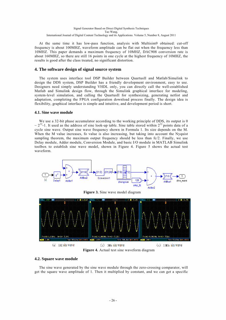
We use a 32-bit phase accumulator according to the working principle of DDS, its output is 0
~ 232-1. It used as the address of sine look-up table. Sine table stored within 232 points data of a cycle sine wave. Output sine wave frequency shown in Formula 1. Its size depends on the M. When the M value increases, fo value is also increasing, but taking into account the Nyquist sampling theorem, the maximum output frequency should be less than fc/2. Finally, we use Delay module, Adder module, Conversion Module, and basic I/O module in MATLAB Simulink toolbox to establish sine wave model, shown in Figure 4. Figure 5 shows the actual test waveform.
Figure 3. Sine wave model diagram
Figure 4. Actual test sine waveform diagram
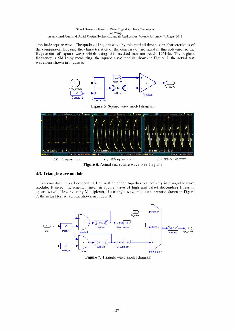
4.2. Square wave module
The sine wave generated by the sine wave module through the zero-crossing comparator, will
get the square wave amplitude of 1. Then it multiplied by constant, and we can get a specific
- 26 -
Signal Generator Based on Direct Digital Synthesis Techniques Tao Wang,
International Journal of Digital Content Technology and its Applications. Volume 5, Number 8, August 2011
amplitude square wave. The quality of square wave by this method depends on characteristics of the comparator. Because the characteristics of the comparator are fixed in this software, so the frequencies of square wave which using this method can not reach 10MHz. The highest frequency is 5MHz by measuring, the square wave module shown in Figure 5, the actual test waveform shown in Figure 6.
Figure 5. Square wave model diagram
Figure 6. Actual test square waveform diagram
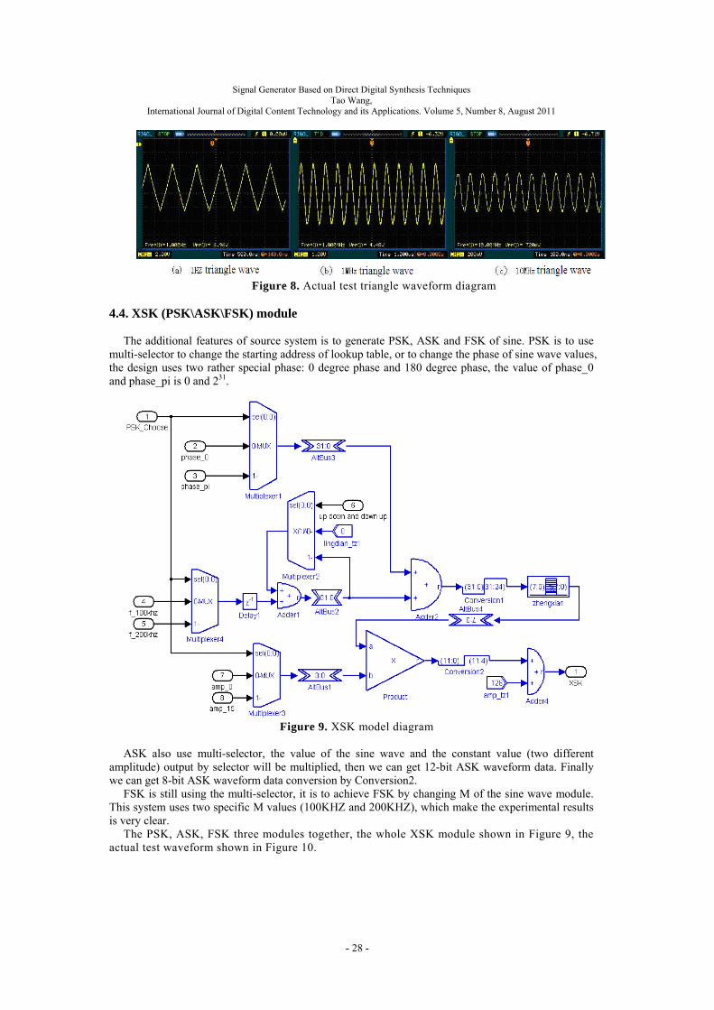
4.3. Triangle wave module Incremental line and descending line will be added together respectively in triangular wave
module. It select incremental linear in square wave of high and select descending linear in square wave of low by using Multiplexer, the triangle wave module schematic shown in Figure 7, the actual test waveform shown in Figure 8.
Figure 7. Triangle wave model diagram
- 27 -
Signal Generator Based on Direct Digital Synthesis Techniques Tao Wang,
International Journal of Digital Content Technology and its Applications. Volume 5, Number 8, August 2011
Figure 8. Actual test triangle waveform diagram
4.4. XSK (PSK\ASK\FSK) module The additional features of source system is to generate PSK, ASK and FSK of sine. PSK is to use
multi-selector to change the starting address of lookup table, or to change the phase of sine wave values, the design uses two rather special phase: 0 degree phase and 180 degree phase, the value of phase_0 and phase_pi is 0 and 231.
Figure 9. XSK model diagram
ASK also use multi-selector, the value of the sine wave and the constant value (two different
amplitude) output by selector will be multiplied, then we can get 12-bit ASK waveform data. Finally we can get 8-bit ASK waveform data conversion by Conversion2.
FSK is still using the multi-selector, it is to achieve FSK by changing M of the sine wave module. This system uses two specific M values (100KHZ and 200KHZ), which make the experimental results is very clear.
The PSK, ASK, FSK three modules together, the whole XSK module shown in Figure 9, the actual test waveform shown in Figure 10.
- 28 -
Signal Generator Based on Direct Digital Synthesis Techniques Tao Wang,
International Journal of Digital Content Technology and its Applications. Volume 5, Number 8, August 2011
Figure 10. Actual test XSK waveform diagram
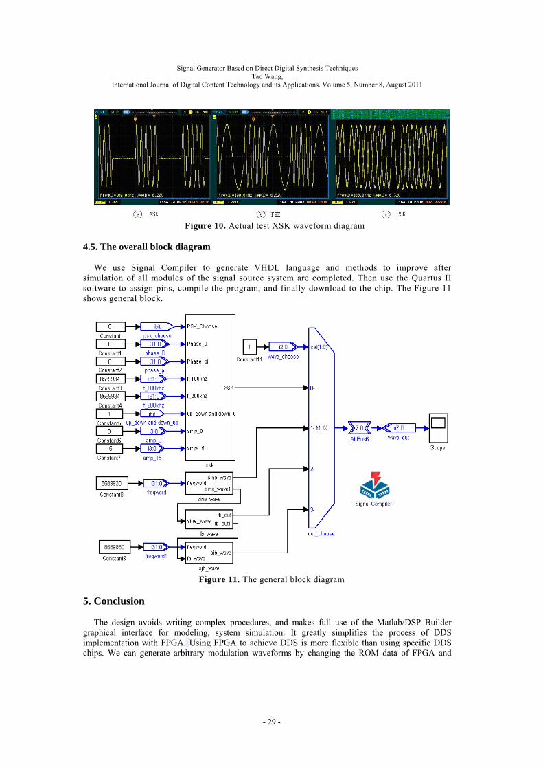
4.5. The overall block diagram We use Signal Compiler to generate VHDL language and methods to improve after
simulation of all modules of the signal source system are completed. Then use the Quartus II software to assign pins, compile the program, and finally download to the chip. The Figure 11 shows general block.
Figure 11. The general block diagram
5. Conclusion
The design avoids writing complex procedures, and makes full use of the Matlab/DSP Builder graphical interface for modeling, system simulation. It greatly simplifies the process of DDS implementation with FPGA. Using FPGA to achieve DDS is more flexible than using specific DDS chips. We can generate arbitrary modulation waveforms by changing the ROM data of FPGA and
- 29 -
Signal Generator Based on Direct Digital Synthesis Techniques Tao Wang,
International Journal of Digital Content Technology and its Applications. Volume 5, Number 8, August 2011
control parameters. Resolution of waveforms is high. Paper, the signal source system can achieve 0~10Mhz sine wave, triangular wave and 0~5Mhz square wave, but also to achieve PSK, FSK, ASK. It is generally meeting the basic application requirements. How to improve the frequency and waveform quality is the next focus of the study. 6. References [1] Shouliang Yang, “Realizes the DDS design using Matlab/DSP Builder”, Microcomputer
Information, vol.22, no.20, pp. 211-213, 2006. [2] Jie Wang, Lin Ma, Weina Liu, Zixu Wang, “The DDS Design based on DSP Builder and FPGA
Implementation”, Modern Electronic Technology, vol.29, no.14, pp.25-27, 2006. [3] Assist. Prof. Dr. Hanan A. R. Akkar, M. Sc. Student Firas R. Mahdi, "Implementation of Digital
Circuits Using Neuro - Swarm Based on FPGA", IJACT, Vol. 2, No. 2, pp. 64-78, 2010. [4] H.T.Nicholas,III H.Samulei, “An analysis of the output spectrum of Direct Digital Frequency
Sythesizers in the presence of phase-accumulator truncation”, IEEE Proc.41st AFCS, pp. 495-502, 1987.
[5] Zhenhua Bai, Xingqun Zhao, Ling Xia, Shuai Yuan, “An Arbitrary Waveform Generator Based on DDS”, Modern Scientific Instruments, vol.48, no.6, pp. 44-47, 2001.
[6] Timo Rahkonen, Harri Eksyma, Antti Mantyniemi, Heikki Repo, “A DDS Synthesizer with Digital Time Domain Interpolator”, Analog Integrated Circuits and Signal Processing, vol.27, no.1, pp.109-116, 2001.
[7] Ali Mohammed Noori Hasan , Lwaa Faisal Abdul Ameer , "Implementation of Digital Chaotic Signal Generator with an Efficient Cross- Correlation in Wireless Communications ", IJACT, Vol. 1, No. 1, pp. 18-23, 2009.
[8] Xuesong YAN, Qinghua WU, Chengyu HU, Qingzhong LIANG, "Electronic Circuits Optimization Design Based On Cultural Algorithms", IJIPM, Vol. 2, No. 1, pp. 49-56, 2011.
- 30 -


