EE101: Digital circuits (Part 4)
M. B. [email protected]
www.ee.iitb.ac.in/~sequel
Department of Electrical EngineeringIndian Institute of Technology Bombay
M. B. Patil, IIT Bombay
Sequential circuits
* The digital circuits we have seen so far (gates, multiplexer, demultiplexer,encoders, decoders) are combinatorial in nature, i.e., the output(s) depends onlyon the present values of the inputs and not on their past values.
* In sequential circuits, the “state” of the circuit is crucial in determining theoutput values. For a given input combination, a sequential circuit may producedifferent output values, depending on its previous state.
* In other words, a sequential circuit has a memory (of its past state) whereas acombinatorial circuit has no memory.
* Sequential circuits (together with combinatorial circuits) make it possible tobuild several useful applications, such as counters, registers, arithmetic/logic unit(ALU), all the way to microprocessors.
M. B. Patil, IIT Bombay
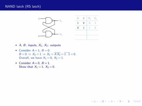
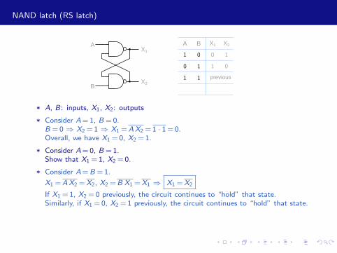
NAND latch (RS latch)
A
B
A B X2X1
X1
X2
1 0 0 1
10 01
previous1 1
1 10 0
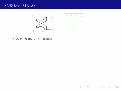
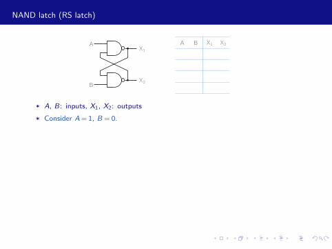
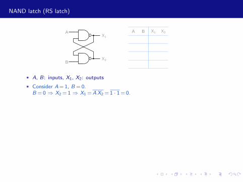
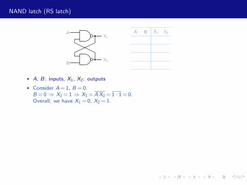
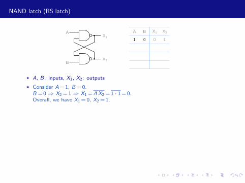
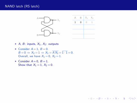
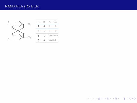
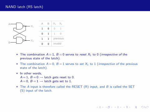
* A, B: inputs, X1, X2: outputs
* Consider A = 1, B = 0.
B = 0 ⇒ X2 = 1 ⇒ X1 = AX2 = 1 · 1 = 0.Overall, we have X1 = 0, X2 = 1.
* Consider A = 0, B = 1.Show that X1 = 1, X2 = 0.
* Consider A = B = 1.
X1 = AX2 = X2, X2 = B X1 = X1 ⇒ X1 = X2
If X1 = 1, X2 = 0 previously, the circuit continues to “hold” that state.Similarly, if X1 = 0, X2 = 1 previously, the circuit continues to “hold” that state.The circuit has “latched in” the previous state.
* For A = B = 0, X1 and X2 are both 1. This combination of A and B is notallowed for reasons that will become clear later.
M. B. Patil, IIT Bombay
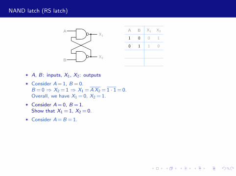
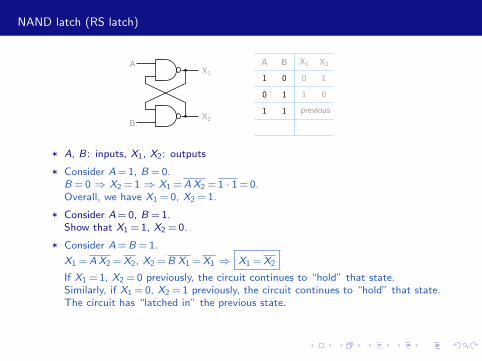
NAND latch (RS latch)
A
B
A B X2X1
X1
X2
1 0 0 1
10 01
previous1 1
1 10 0
* A, B: inputs, X1, X2: outputs
* Consider A = 1, B = 0.
B = 0 ⇒ X2 = 1 ⇒ X1 = A X2 = 1 · 1 = 0.Overall, we have X1 = 0, X2 = 1.
* Consider A = 0, B = 1.Show that X1 = 1, X2 = 0.
* Consider A = B = 1.
X1 = AX2 = X2, X2 = B X1 = X1 ⇒ X1 = X2
If X1 = 1, X2 = 0 previously, the circuit continues to “hold” that state.Similarly, if X1 = 0, X2 = 1 previously, the circuit continues to “hold” that state.The circuit has “latched in” the previous state.
* For A = B = 0, X1 and X2 are both 1. This combination of A and B is notallowed for reasons that will become clear later.
M. B. Patil, IIT Bombay
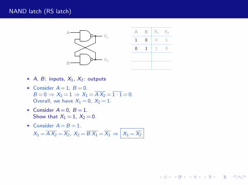
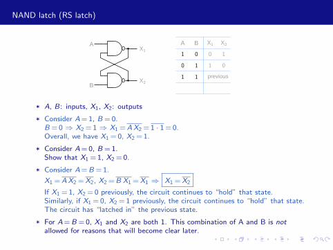
NAND latch (RS latch)
A
B
A B X2X1
X1
X2
1 0 0 1
10 01
previous1 1
1 10 0
* A, B: inputs, X1, X2: outputs
* Consider A = 1, B = 0.B = 0 ⇒ X2 = 1 ⇒ X1 = AX2 = 1 · 1 = 0.
Overall, we have X1 = 0, X2 = 1.
* Consider A = 0, B = 1.Show that X1 = 1, X2 = 0.
* Consider A = B = 1.
X1 = AX2 = X2, X2 = B X1 = X1 ⇒ X1 = X2
If X1 = 1, X2 = 0 previously, the circuit continues to “hold” that state.Similarly, if X1 = 0, X2 = 1 previously, the circuit continues to “hold” that state.The circuit has “latched in” the previous state.
* For A = B = 0, X1 and X2 are both 1. This combination of A and B is notallowed for reasons that will become clear later.
M. B. Patil, IIT Bombay
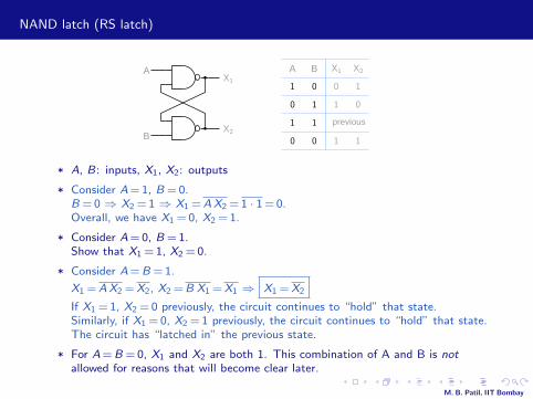
NAND latch (RS latch)
A
B
A B X2X1
X1
X2
1 0 0 1
10 01
previous1 1
1 10 0
* A, B: inputs, X1, X2: outputs
* Consider A = 1, B = 0.B = 0 ⇒ X2 = 1 ⇒ X1 = AX2 = 1 · 1 = 0.Overall, we have X1 = 0, X2 = 1.
* Consider A = 0, B = 1.Show that X1 = 1, X2 = 0.
* Consider A = B = 1.
X1 = AX2 = X2, X2 = B X1 = X1 ⇒ X1 = X2
If X1 = 1, X2 = 0 previously, the circuit continues to “hold” that state.Similarly, if X1 = 0, X2 = 1 previously, the circuit continues to “hold” that state.The circuit has “latched in” the previous state.
* For A = B = 0, X1 and X2 are both 1. This combination of A and B is notallowed for reasons that will become clear later.
M. B. Patil, IIT Bombay
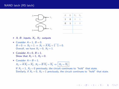
NAND latch (RS latch)
A
B
A B X2X1
X1
X2
1 0 0 1
10 01
previous1 1
1 10 0
* A, B: inputs, X1, X2: outputs
* Consider A = 1, B = 0.B = 0 ⇒ X2 = 1 ⇒ X1 = AX2 = 1 · 1 = 0.Overall, we have X1 = 0, X2 = 1.
* Consider A = 0, B = 1.Show that X1 = 1, X2 = 0.
* Consider A = B = 1.
X1 = AX2 = X2, X2 = B X1 = X1 ⇒ X1 = X2
If X1 = 1, X2 = 0 previously, the circuit continues to “hold” that state.Similarly, if X1 = 0, X2 = 1 previously, the circuit continues to “hold” that state.The circuit has “latched in” the previous state.
* For A = B = 0, X1 and X2 are both 1. This combination of A and B is notallowed for reasons that will become clear later.
M. B. Patil, IIT Bombay
NAND latch (RS latch)
A
B
A B X2X1
X1
X2
1 0 0 1
10 01
previous1 1
1 10 0
* A, B: inputs, X1, X2: outputs
* Consider A = 1, B = 0.B = 0 ⇒ X2 = 1 ⇒ X1 = AX2 = 1 · 1 = 0.Overall, we have X1 = 0, X2 = 1.
* Consider A = 0, B = 1.Show that X1 = 1, X2 = 0.
* Consider A = B = 1.
X1 = A X2 = X2, X2 = B X1 = X1 ⇒ X1 = X2
If X1 = 1, X2 = 0 previously, the circuit continues to “hold” that state.Similarly, if X1 = 0, X2 = 1 previously, the circuit continues to “hold” that state.The circuit has “latched in” the previous state.
* For A = B = 0, X1 and X2 are both 1. This combination of A and B is notallowed for reasons that will become clear later.
M. B. Patil, IIT Bombay
NAND latch (RS latch)
A
B
A B X2X1
X1
X2
1 0 0 1
10 01
previous1 1
1 10 0
* A, B: inputs, X1, X2: outputs
* Consider A = 1, B = 0.B = 0 ⇒ X2 = 1 ⇒ X1 = AX2 = 1 · 1 = 0.Overall, we have X1 = 0, X2 = 1.
* Consider A = 0, B = 1.Show that X1 = 1, X2 = 0.
* Consider A = B = 1.
X1 = AX2 = X2, X2 = B X1 = X1 ⇒ X1 = X2
If X1 = 1, X2 = 0 previously, the circuit continues to “hold” that state.Similarly, if X1 = 0, X2 = 1 previously, the circuit continues to “hold” that state.The circuit has “latched in” the previous state.
* For A = B = 0, X1 and X2 are both 1. This combination of A and B is notallowed for reasons that will become clear later.
M. B. Patil, IIT Bombay
NAND latch (RS latch)
A
B
A B X2X1
X1
X2
1 0 0 1
10 01
previous1 1
1 10 0
* A, B: inputs, X1, X2: outputs
* Consider A = 1, B = 0.B = 0 ⇒ X2 = 1 ⇒ X1 = AX2 = 1 · 1 = 0.Overall, we have X1 = 0, X2 = 1.
* Consider A = 0, B = 1.Show that X1 = 1, X2 = 0.
* Consider A = B = 1.
X1 = AX2 = X2, X2 = B X1 = X1 ⇒ X1 = X2
If X1 = 1, X2 = 0 previously, the circuit continues to “hold” that state.Similarly, if X1 = 0, X2 = 1 previously, the circuit continues to “hold” that state.
The circuit has “latched in” the previous state.
* For A = B = 0, X1 and X2 are both 1. This combination of A and B is notallowed for reasons that will become clear later.
M. B. Patil, IIT Bombay
NAND latch (RS latch)
A
B
A B X2X1
X1
X2
1 0 0 1
10 01
previous1 1
1 10 0
* A, B: inputs, X1, X2: outputs
* Consider A = 1, B = 0.B = 0 ⇒ X2 = 1 ⇒ X1 = AX2 = 1 · 1 = 0.Overall, we have X1 = 0, X2 = 1.
* Consider A = 0, B = 1.Show that X1 = 1, X2 = 0.
* Consider A = B = 1.
X1 = AX2 = X2, X2 = B X1 = X1 ⇒ X1 = X2
If X1 = 1, X2 = 0 previously, the circuit continues to “hold” that state.Similarly, if X1 = 0, X2 = 1 previously, the circuit continues to “hold” that state.The circuit has “latched in” the previous state.
* For A = B = 0, X1 and X2 are both 1. This combination of A and B is notallowed for reasons that will become clear later.
M. B. Patil, IIT Bombay
NAND latch (RS latch)
A
B
A B X2X1
X1
X2
1 0 0 1
10 01
previous1 1
1 10 0
* A, B: inputs, X1, X2: outputs
* Consider A = 1, B = 0.B = 0 ⇒ X2 = 1 ⇒ X1 = AX2 = 1 · 1 = 0.Overall, we have X1 = 0, X2 = 1.
* Consider A = 0, B = 1.Show that X1 = 1, X2 = 0.
* Consider A = B = 1.
X1 = AX2 = X2, X2 = B X1 = X1 ⇒ X1 = X2
If X1 = 1, X2 = 0 previously, the circuit continues to “hold” that state.Similarly, if X1 = 0, X2 = 1 previously, the circuit continues to “hold” that state.The circuit has “latched in” the previous state.
* For A = B = 0, X1 and X2 are both 1. This combination of A and B is notallowed for reasons that will become clear later.
M. B. Patil, IIT Bombay
NAND latch (RS latch)
A BA
B
previous
invalid
X2X1
1
1
1 1
0
0
0
0
1
1
0 0
X1
X2
R S
previous
R
S invalid
1
1
1 1
0
0
0
0
1
1
0 0
QQQ
Q
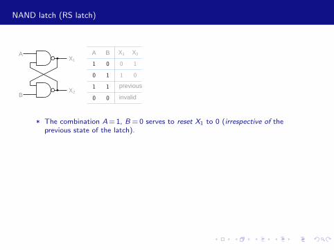
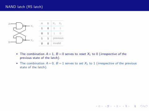
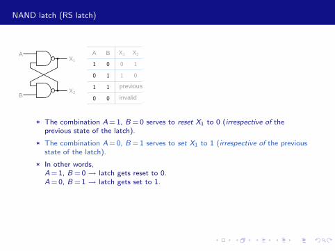
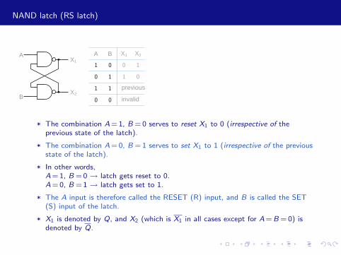
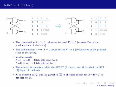
* The combination A = 1, B = 0 serves to reset X1 to 0 (irrespective of theprevious state of the latch).
* The combination A = 0, B = 1 serves to set X1 to 1 (irrespective of the previousstate of the latch).
* In other words,A = 1, B = 0 → latch gets reset to 0.A = 0, B = 1 → latch gets set to 1.
* The A input is therefore called the RESET (R) input, and B is called the SET(S) input of the latch.
* X1 is denoted by Q, and X2 (which is X1 in all cases except for A = B = 0) isdenoted by Q.
M. B. Patil, IIT Bombay
NAND latch (RS latch)
A BA
B
previous
invalid
X2X1
1
1
1 1
0
0
0
0
1
1
0 0
X1
X2
R S
previous
R
S invalid
1
1
1 1
0
0
0
0
1
1
0 0
QQQ
Q
* The combination A = 1, B = 0 serves to reset X1 to 0 (irrespective of theprevious state of the latch).
* The combination A = 0, B = 1 serves to set X1 to 1 (irrespective of the previousstate of the latch).
* In other words,A = 1, B = 0 → latch gets reset to 0.A = 0, B = 1 → latch gets set to 1.
* The A input is therefore called the RESET (R) input, and B is called the SET(S) input of the latch.
* X1 is denoted by Q, and X2 (which is X1 in all cases except for A = B = 0) isdenoted by Q.
M. B. Patil, IIT Bombay

NAND latch (RS latch)
R S
previous
R
S invalid
R
S
t
t
t
tt2 t3t1
1
1
1 1
0
0
0
0
1
1
0 0
QQQ
Q
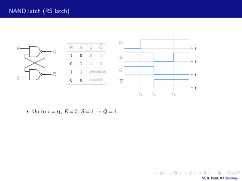
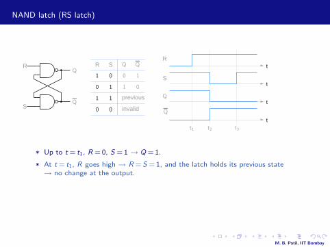
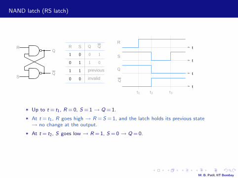
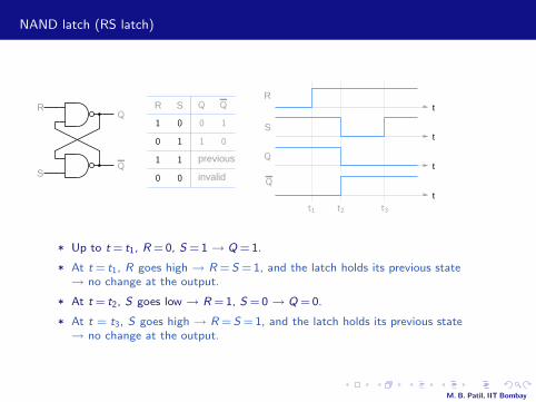
* Up to t = t1, R = 0, S = 1 → Q = 1.
* At t = t1, R goes high → R = S = 1, and the latch holds its previous state→ no change at the output.
* At t = t2, S goes low → R = 1, S = 0 → Q = 0.
* At t = t3, S goes high → R = S = 1, and the latch holds its previous state→ no change at the output.
M. B. Patil, IIT Bombay
NAND latch (RS latch)
R S
previous
R
S invalid
R
S
t
t
t
tt2 t3t1
1
1
1 1
0
0
0
0
1
1
0 0
QQQ
Q
* Up to t = t1, R = 0, S = 1 → Q = 1.
* At t = t1, R goes high → R = S = 1, and the latch holds its previous state→ no change at the output.
* At t = t2, S goes low → R = 1, S = 0 → Q = 0.
* At t = t3, S goes high → R = S = 1, and the latch holds its previous state→ no change at the output.
M. B. Patil, IIT Bombay
NAND latch (RS latch)
R
S
R S t
t
t
t
previous
R
S
t3t2t1
1
1
1 1
0
0
0
0
1
1
0 0 1 1
Q
Q
Q
Q
t4 t5
?
?
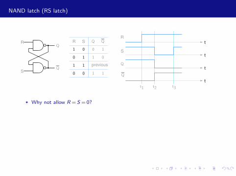
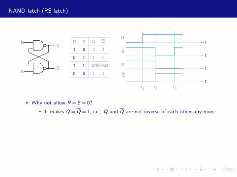
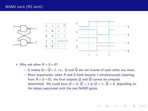
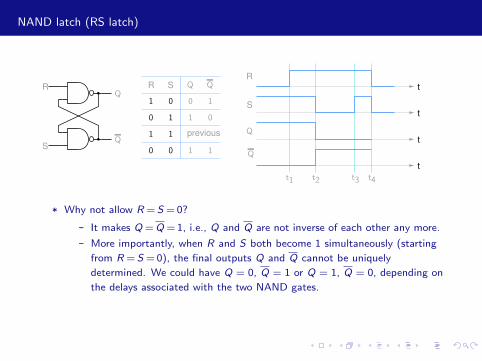
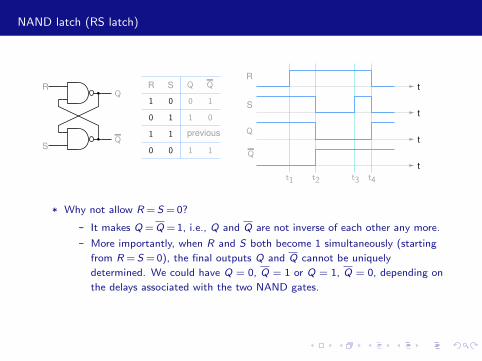
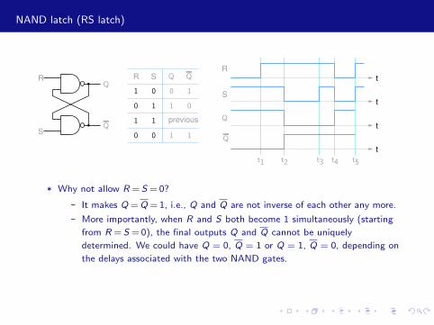
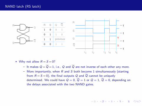
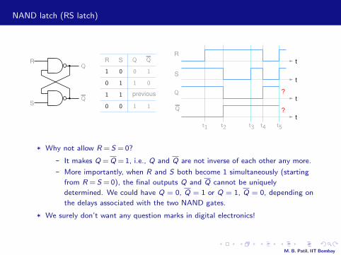
* Why not allow R = S = 0?
- It makes Q = Q = 1, i.e., Q and Q are not inverse of each other any more.
- More importantly, when R and S both become 1 simultaneously (starting
from R = S = 0), the final outputs Q and Q cannot be uniquely
determined. We could have Q = 0, Q = 1 or Q = 1, Q = 0, depending on
the delays associated with the two NAND gates.
* We surely don’t want any question marks in digital electronics!
M. B. Patil, IIT Bombay
NAND latch (RS latch)
R
S
R S t
t
t
t
previous
R
S
t3t2t1
1
1
1 1
0
0
0
0
1
1
0 0 1 1
Q
Q
Q
Q
t4 t5
?
?
* Why not allow R = S = 0?
- It makes Q = Q = 1, i.e., Q and Q are not inverse of each other any more.
- More importantly, when R and S both become 1 simultaneously (starting
from R = S = 0), the final outputs Q and Q cannot be uniquely
determined. We could have Q = 0, Q = 1 or Q = 1, Q = 0, depending on
the delays associated with the two NAND gates.
* We surely don’t want any question marks in digital electronics!
M. B. Patil, IIT Bombay
NAND latch (RS latch)
R
S
R S t
t
t
t
previous
R
S
t3t2t1
1
1
1 1
0
0
0
0
1
1
0 0 1 1
Q
Q
Q
Q
t4
t5
?
?
* Why not allow R = S = 0?
- It makes Q = Q = 1, i.e., Q and Q are not inverse of each other any more.
- More importantly, when R and S both become 1 simultaneously (starting
from R = S = 0), the final outputs Q and Q cannot be uniquely
determined. We could have Q = 0, Q = 1 or Q = 1, Q = 0, depending on
the delays associated with the two NAND gates.
* We surely don’t want any question marks in digital electronics!
M. B. Patil, IIT Bombay
NAND latch (RS latch)
R
S
R S t
t
t
t
previous
R
S
t3t2t1
1
1
1 1
0
0
0
0
1
1
0 0 1 1
Q
Q
Q
Q
t4 t5
?
?
* Why not allow R = S = 0?
- It makes Q = Q = 1, i.e., Q and Q are not inverse of each other any more.
- More importantly, when R and S both become 1 simultaneously (starting
from R = S = 0), the final outputs Q and Q cannot be uniquely
determined. We could have Q = 0, Q = 1 or Q = 1, Q = 0, depending on
the delays associated with the two NAND gates.
* We surely don’t want any question marks in digital electronics!
M. B. Patil, IIT Bombay
NAND latch (RS latch)
R
S
R S t
t
t
t
previous
R
S
t3t2t1
1
1
1 1
0
0
0
0
1
1
0 0 1 1
Q
Q
Q
Q
t4 t5
?
?
* Why not allow R = S = 0?
- It makes Q = Q = 1, i.e., Q and Q are not inverse of each other any more.
- More importantly, when R and S both become 1 simultaneously (starting
from R = S = 0), the final outputs Q and Q cannot be uniquely
determined. We could have Q = 0, Q = 1 or Q = 1, Q = 0, depending on
the delays associated with the two NAND gates.
* We surely don’t want any question marks in digital electronics!
M. B. Patil, IIT Bombay
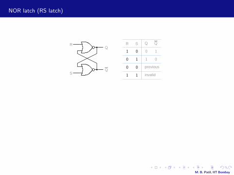
NOR latch (RS latch)
R S
previous
invalid
R
S
1
1
0
0
0
0
1
1
1 1
00
QQQ
Q
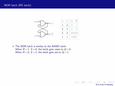
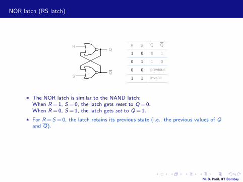
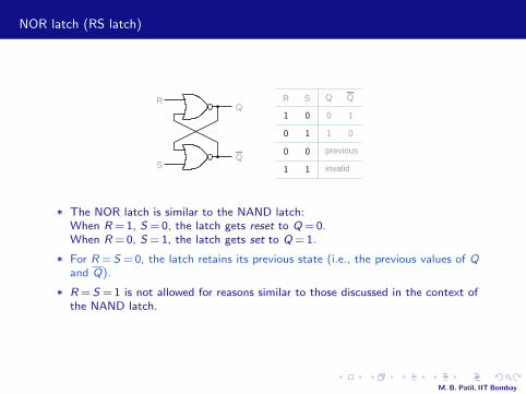
* The NOR latch is similar to the NAND latch:When R = 1, S = 0, the latch gets reset to Q = 0.When R = 0, S = 1, the latch gets set to Q = 1.
* For R = S = 0, the latch retains its previous state (i.e., the previous values of Qand Q).
* R = S = 1 is not allowed for reasons similar to those discussed in the context ofthe NAND latch.
M. B. Patil, IIT Bombay
NOR latch (RS latch)
R S
previous
invalid
R
S
1
1
0
0
0
0
1
1
1 1
00
QQQ
Q
* The NOR latch is similar to the NAND latch:When R = 1, S = 0, the latch gets reset to Q = 0.When R = 0, S = 1, the latch gets set to Q = 1.
* For R = S = 0, the latch retains its previous state (i.e., the previous values of Qand Q).
* R = S = 1 is not allowed for reasons similar to those discussed in the context ofthe NAND latch.
M. B. Patil, IIT Bombay
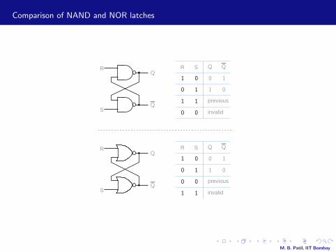
Comparison of NAND and NOR latches
R S
previous
invalid
R
S
R S
previous
invalid
R
S
1
1
0
0
0
0
1
1
1 1
00
1
1
1 1
0
0
0
0
1
1
0 0
QQQ
Q
QQQ
Q
M. B. Patil, IIT Bombay
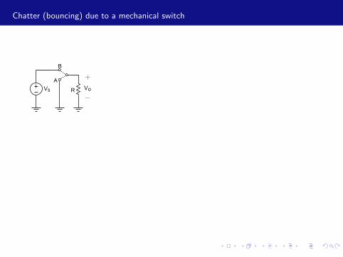
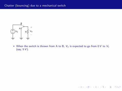
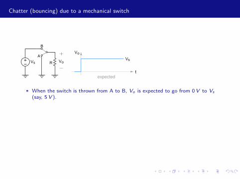
Chatter (bouncing) due to a mechanical switch
R
B
A
Vs Vo
texpected
Vs
Vo
t
actual
Vs
Vo
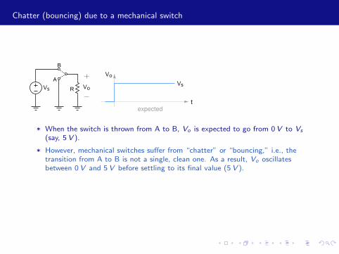
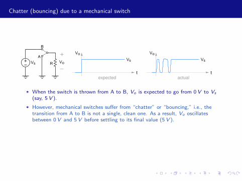
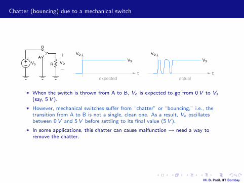
* When the switch is thrown from A to B, Vo is expected to go from 0 V to Vs
(say, 5 V ).
* However, mechanical switches suffer from “chatter” or “bouncing,” i.e., thetransition from A to B is not a single, clean one. As a result, Vo oscillatesbetween 0 V and 5 V before settling to its final value (5 V ).
* In some applications, this chatter can cause malfunction → need a way toremove the chatter.
M. B. Patil, IIT Bombay
Chatter (bouncing) due to a mechanical switch
R
B
A
Vs Vo
texpected
Vs
Vo
t
actual
Vs
Vo
* When the switch is thrown from A to B, Vo is expected to go from 0 V to Vs
(say, 5 V ).
* However, mechanical switches suffer from “chatter” or “bouncing,” i.e., thetransition from A to B is not a single, clean one. As a result, Vo oscillatesbetween 0 V and 5 V before settling to its final value (5 V ).
* In some applications, this chatter can cause malfunction → need a way toremove the chatter.
M. B. Patil, IIT Bombay
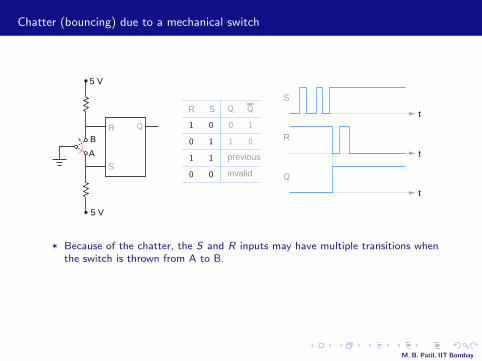
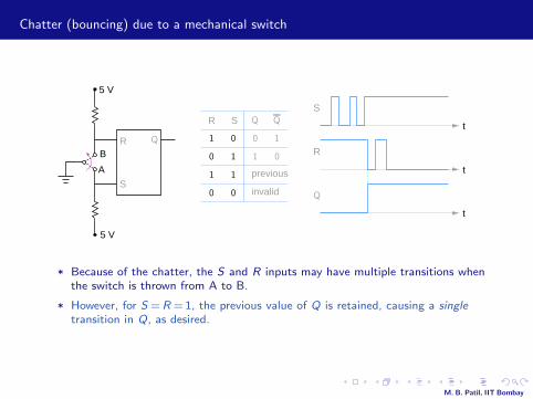
Chatter (bouncing) due to a mechanical switch
A
BR
S
5 V
5 V
R S
previous
invalid
R
S
t
t
t1
1
1 1
0
0
0
0
1
1
0 0
Q
Q
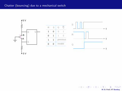
* Because of the chatter, the S and R inputs may have multiple transitions whenthe switch is thrown from A to B.
* However, for S = R = 1, the previous value of Q is retained, causing a singletransition in Q, as desired.
M. B. Patil, IIT Bombay
Chatter (bouncing) due to a mechanical switch
A
BR
S
5 V
5 V
R S
previous
invalid
R
S
t
t
t1
1
1 1
0
0
0
0
1
1
0 0
Q
Q
* Because of the chatter, the S and R inputs may have multiple transitions whenthe switch is thrown from A to B.
* However, for S = R = 1, the previous value of Q is retained, causing a singletransition in Q, as desired.
M. B. Patil, IIT Bombay
The “clock”
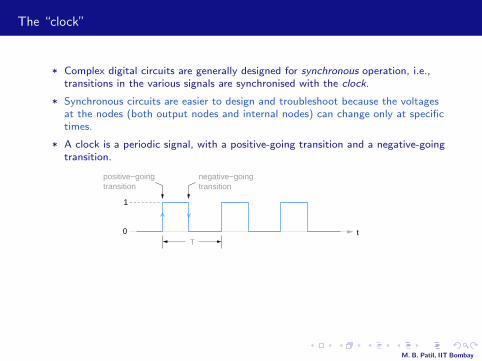
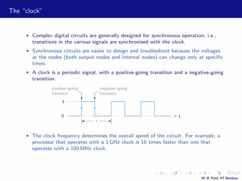
* Complex digital circuits are generally designed for synchronous operation, i.e.,transitions in the various signals are synchronised with the clock.
* Synchronous circuits are easier to design and troubleshoot because the voltagesat the nodes (both output nodes and internal nodes) can change only at specifictimes.
* A clock is a periodic signal, with a positive-going transition and a negative-goingtransition.
negative−goingtransition
t0
1
positive−goingtransition
T
* The clock frequency determines the overall speed of the circuit. For example, aprocessor that operates with a 1 GHz clock is 10 times faster than one thatoperates with a 100 MHz clock.
M. B. Patil, IIT Bombay
The “clock”
* Complex digital circuits are generally designed for synchronous operation, i.e.,transitions in the various signals are synchronised with the clock.
* Synchronous circuits are easier to design and troubleshoot because the voltagesat the nodes (both output nodes and internal nodes) can change only at specifictimes.
* A clock is a periodic signal, with a positive-going transition and a negative-goingtransition.
negative−goingtransition
t0
1
positive−goingtransition
T
* The clock frequency determines the overall speed of the circuit. For example, aprocessor that operates with a 1 GHz clock is 10 times faster than one thatoperates with a 100 MHz clock.
M. B. Patil, IIT Bombay
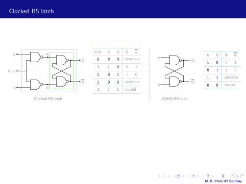
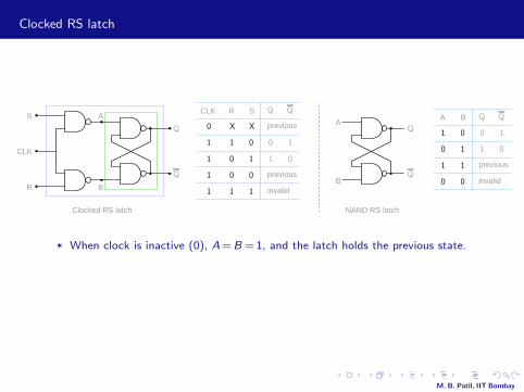
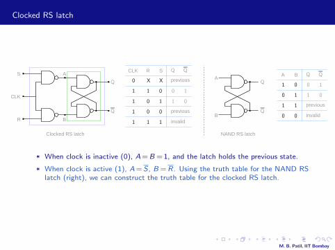
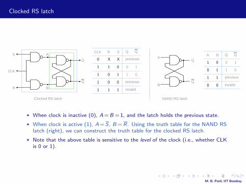
Clocked RS latch
R
S
CLK
A
B
R SCLK
previous
invalid
previous A
B
A B
previous
invalid
Clocked RS latch NAND RS latch
1
1
0
0
0
0
1
1
0 0
11
1
1
1
1
0 X X1
1
1 1
0
0
0
0
1
1
0 0
Q
Q
Q
Q
* When clock is inactive (0), A = B = 1, and the latch holds the previous state.
* When clock is active (1), A = S , B = R. Using the truth table for the NAND RSlatch (right), we can construct the truth table for the clocked RS latch.
* Note that the above table is sensitive to the level of the clock (i.e., whether CLKis 0 or 1).
M. B. Patil, IIT Bombay
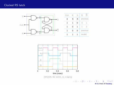
Clocked RS latch
R
S
CLK
A
B
R SCLK
previous
invalid
previous
CLK
S
Q
R
(SEQUEL file: ee101_rs_1.sqproj)
time (msec) 0 0.2 0.4 0.6 0.8
1
1
0
0
0
0
1
1
0 0
11
1
1
1
1
0 X XQ
Q
M. B. Patil, IIT Bombay
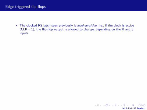
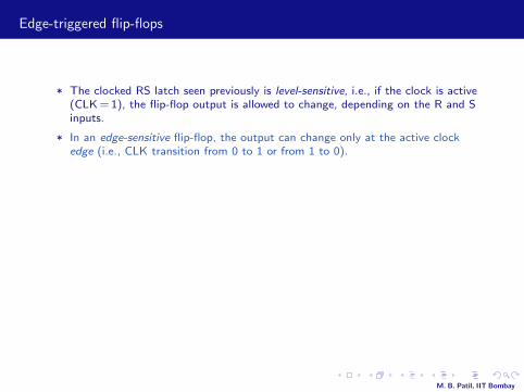
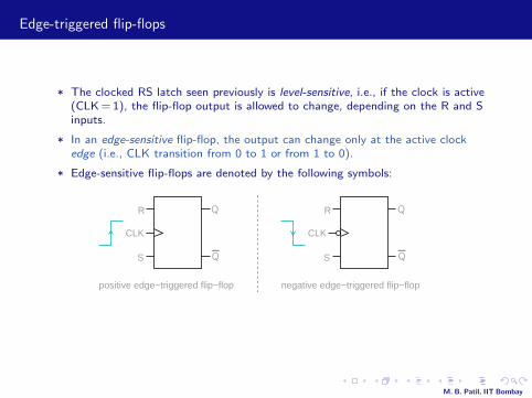
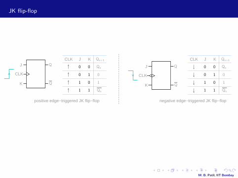
Edge-triggered flip-flops
* The clocked RS latch seen previously is level-sensitive, i.e., if the clock is active(CLK = 1), the flip-flop output is allowed to change, depending on the R and Sinputs.
* In an edge-sensitive flip-flop, the output can change only at the active clockedge (i.e., CLK transition from 0 to 1 or from 1 to 0).
* Edge-sensitive flip-flops are denoted by the following symbols:
R
CLK
S
positive edge−triggered flip−flop negative edge−triggered flip−flop
R
S
CLK
Q
Q
Q
Q
M. B. Patil, IIT Bombay
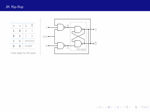
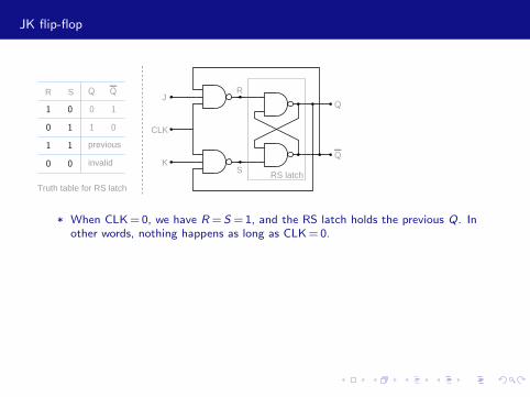
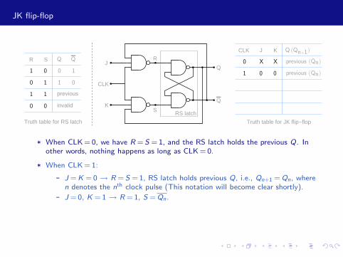
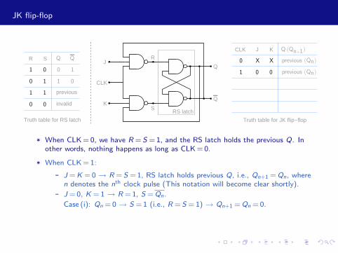
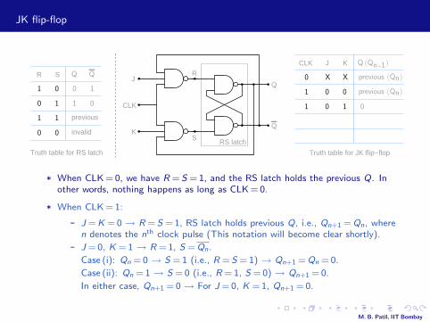
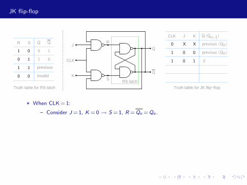
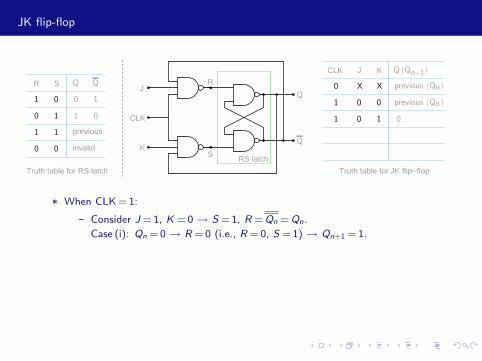
JK flip-flop
S
R
CLK
J
KRS latch
R S
previous
invalid
Truth table for RS latch
1
1
1 1
0
0
0
0
1
1
0 0
Q
Q
CLK KJ
Truth table for JK flip−flop
0 XX previous (Qn)
Q (Qn+1)
1 0 0 previous (Qn)
1 10 0
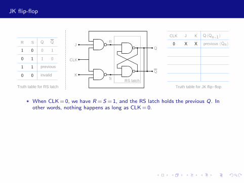
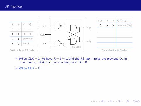
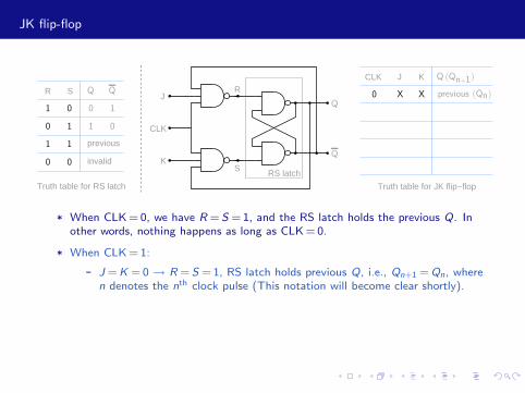
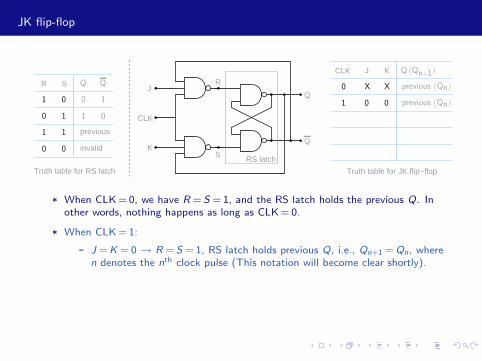
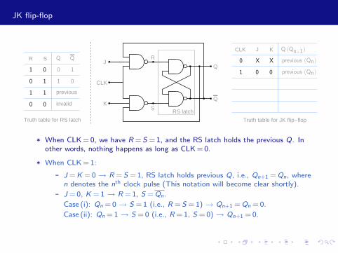
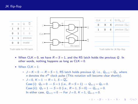
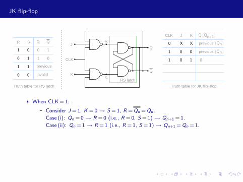
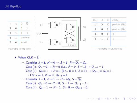
* When CLK = 0, we have R = S = 1, and the RS latch holds the previous Q. Inother words, nothing happens as long as CLK = 0.
* When CLK = 1:
- J = K = 0 → R = S = 1, RS latch holds previous Q, i.e., Qn+1 = Qn, wheren denotes the nth clock pulse (This notation will become clear shortly).
- J = 0, K = 1 → R = 1, S = Qn.
Case (i): Qn = 0 → S = 1 (i.e., R = S = 1) → Qn+1 = Qn = 0.
Case (ii): Qn = 1 → S = 0 (i.e., R = 1, S = 0) → Qn+1 = 0.
In either case, Qn+1 = 0 → For J = 0, K = 1, Qn+1 = 0.
M. B. Patil, IIT Bombay
JK flip-flop
S
R
CLK
J
KRS latch
R S
previous
invalid
Truth table for RS latch
1
1
1 1
0
0
0
0
1
1
0 0
Q
Q
CLK KJ
Truth table for JK flip−flop
0 XX previous (Qn)
Q (Qn+1)
1 0 0 previous (Qn)
1 10 0
* When CLK = 0, we have R = S = 1, and the RS latch holds the previous Q. Inother words, nothing happens as long as CLK = 0.
* When CLK = 1:
- J = K = 0 → R = S = 1, RS latch holds previous Q, i.e., Qn+1 = Qn, wheren denotes the nth clock pulse (This notation will become clear shortly).
- J = 0, K = 1 → R = 1, S = Qn.
Case (i): Qn = 0 → S = 1 (i.e., R = S = 1) → Qn+1 = Qn = 0.
Case (ii): Qn = 1 → S = 0 (i.e., R = 1, S = 0) → Qn+1 = 0.
In either case, Qn+1 = 0 → For J = 0, K = 1, Qn+1 = 0.
M. B. Patil, IIT Bombay
JK flip-flop
S
R
CLK
J
KRS latch
R S
previous
invalid
CLK KJ
Truth table for JK flip−flopTruth table for RS latch
1
1
1 1
0
0
0
0
1
1
0 0
1 0 0
1 10 0
previous (Qn)
0 XX previous (Qn)Q
Q (Qn+1)
Q
1 1 0 1
1 1 1 toggles (Qn)
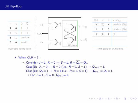
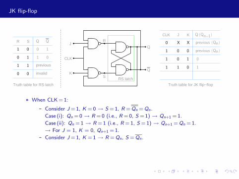
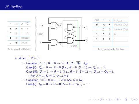
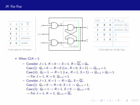
* When CLK = 1:
- Consider J = 1, K = 0 → S = 1, R = Qn = Qn.
Case (i): Qn = 0 → R = 0 (i.e., R = 0, S = 1) → Qn+1 = 1.
Case (ii): Qn = 1 → R = 1 (i.e., R = 1, S = 1) → Qn+1 = Qn = 1.
→ For J = 1, K = 0, Qn+1 = 1.
- Consider J = 1, K = 1 → R = Qn, S = Qn.
Case (i): Qn = 0 → R = 0, S = 1 → Qn+1 = 1.
Case (ii): Qn = 1 → R = 1, S = 0 → Qn+1 = 0.
→ For J = 1, K = 1, Qn+1 = Qn.
M. B. Patil, IIT Bombay
JK flip-flop
S
R
CLK
J
KRS latch
R S
previous
invalid
CLK KJ
Truth table for JK flip−flopTruth table for RS latch
1
1
1 1
0
0
0
0
1
1
0 0
1 0 0
1 10 0
previous (Qn)
0 XX previous (Qn)Q
Q (Qn+1)
Q
1 1 0 1
1 1 1 toggles (Qn)
* When CLK = 1:
- Consider J = 1, K = 0 → S = 1, R = Qn = Qn.
Case (i): Qn = 0 → R = 0 (i.e., R = 0, S = 1) → Qn+1 = 1.
Case (ii): Qn = 1 → R = 1 (i.e., R = 1, S = 1) → Qn+1 = Qn = 1.
→ For J = 1, K = 0, Qn+1 = 1.
- Consider J = 1, K = 1 → R = Qn, S = Qn.
Case (i): Qn = 0 → R = 0, S = 1 → Qn+1 = 1.
Case (ii): Qn = 1 → R = 1, S = 0 → Qn+1 = 0.
→ For J = 1, K = 1, Qn+1 = Qn.
M. B. Patil, IIT Bombay

JK flip-flop
S
R
CLK
J
KRS latch
R S
previous
invalid
CLK KJ
Truth table for JK flip−flopTruth table for RS latch
1
1
1 1
0
0
0
0
1
1
0 0
1 0 0
1 10 0
previous (Qn)
0 XX previous (Qn)Q
Q (Qn+1)
Q1 1 0 1
1 1 1 toggles (Qn)
* When CLK = 1:
- Consider J = 1, K = 0 → S = 1, R = Qn = Qn.
Case (i): Qn = 0 → R = 0 (i.e., R = 0, S = 1) → Qn+1 = 1.
Case (ii): Qn = 1 → R = 1 (i.e., R = 1, S = 1) → Qn+1 = Qn = 1.
→ For J = 1, K = 0, Qn+1 = 1.
- Consider J = 1, K = 1 → R = Qn, S = Qn.
Case (i): Qn = 0 → R = 0, S = 1 → Qn+1 = 1.
Case (ii): Qn = 1 → R = 1, S = 0 → Qn+1 = 0.
→ For J = 1, K = 1, Qn+1 = Qn.
M. B. Patil, IIT Bombay
JK flip-flop
S
R
CLK
J
KRS latch
CLK KJ
Truth table for JK flip−flop
1 0 0
1 10
1 1 0
1 1 1
0
1
previous (Qn)
toggles (Qn)
0 XX previous (Qn)Q
Q (Qn+1)
Q
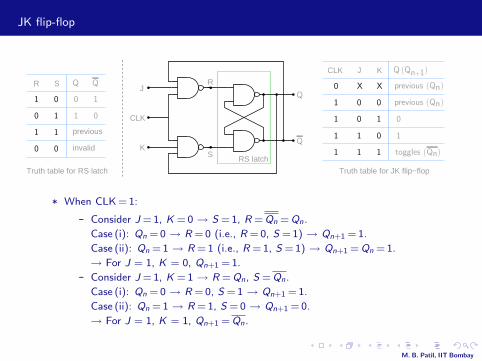
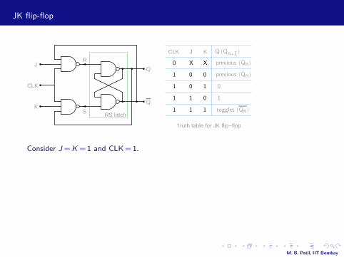
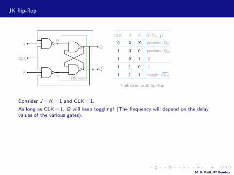
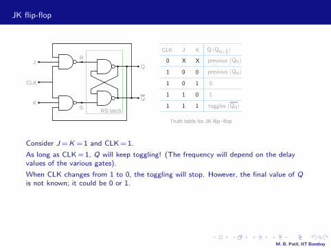
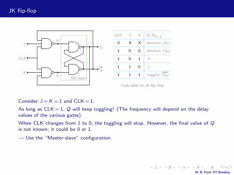
Consider J = K = 1 and CLK = 1.
As long as CLK = 1, Q will keep toggling! (The frequency will depend on the delayvalues of the various gates).
When CLK changes from 1 to 0, the toggling will stop. However, the final value of Qis not known; it could be 0 or 1.
→ Use the “Master-slave” configuration.
M. B. Patil, IIT Bombay
JK flip-flop
S
R
CLK
J
KRS latch
CLK KJ
Truth table for JK flip−flop
1 0 0
1 10
1 1 0
1 1 1
0
1
previous (Qn)
toggles (Qn)
0 XX previous (Qn)Q
Q (Qn+1)
Q
Consider J = K = 1 and CLK = 1.
As long as CLK = 1, Q will keep toggling! (The frequency will depend on the delayvalues of the various gates).
When CLK changes from 1 to 0, the toggling will stop. However, the final value of Qis not known; it could be 0 or 1.
→ Use the “Master-slave” configuration.
M. B. Patil, IIT Bombay
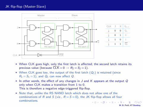
JK flip-flop (Master-Slave)
J
K
SlaveMaster
RS latch 2RS latch 1
Q
CLK CLK
CLK KJ
0 0
0 1
1 0
1 1
Qn
0
1
Qn
Qn+1
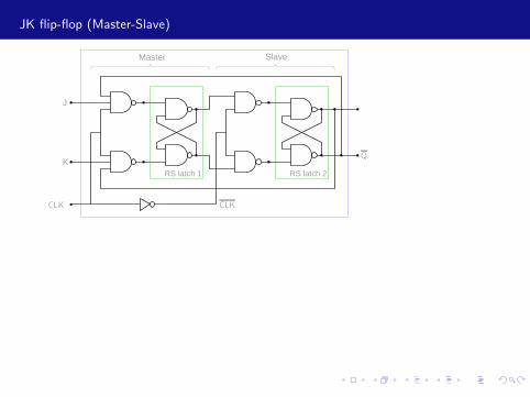
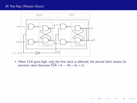
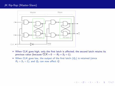
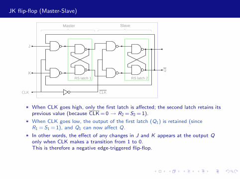
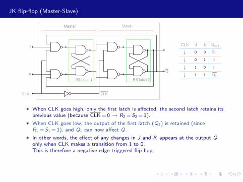
* When CLK goes high, only the first latch is affected; the second latch retains itsprevious value (because CLK = 0 → R2 = S2 = 1).
* When CLK goes low, the output of the first latch (Q1) is retained (sinceR1 = S1 = 1), and Q1 can now affect Q.
* In other words, the effect of any changes in J and K appears at the output Qonly when CLK makes a transition from 1 to 0.This is therefore a negative edge-triggered flip-flop.
* Note that, unlike the RS NAND latch which does not allow one of thecombinations of R and S (viz., R = S = 0), the JK flip-flop allows all fourcombinations.
M. B. Patil, IIT Bombay
JK flip-flop (Master-Slave)
J
K
SlaveMaster
RS latch 2RS latch 1
Q
CLK CLK
CLK KJ
0 0
0 1
1 0
1 1
Qn
0
1
Qn
Qn+1
* When CLK goes high, only the first latch is affected; the second latch retains itsprevious value (because CLK = 0 → R2 = S2 = 1).
* When CLK goes low, the output of the first latch (Q1) is retained (sinceR1 = S1 = 1), and Q1 can now affect Q.
* In other words, the effect of any changes in J and K appears at the output Qonly when CLK makes a transition from 1 to 0.This is therefore a negative edge-triggered flip-flop.
* Note that, unlike the RS NAND latch which does not allow one of thecombinations of R and S (viz., R = S = 0), the JK flip-flop allows all fourcombinations.
M. B. Patil, IIT Bombay
JK flip-flop
CLK
J
K
CLK KJ
positive edge−triggered JK flip−flop
CLK
J
K
CLK KJ
negative edge−triggered JK flip−flop
Q
Q 0 0
0 1
1 0
1 1
Qn
0
1
Qn
0 0
0 1
1 0
1 1
Qn
0
1
Qn
Qn+1
Q
Q
Qn+1
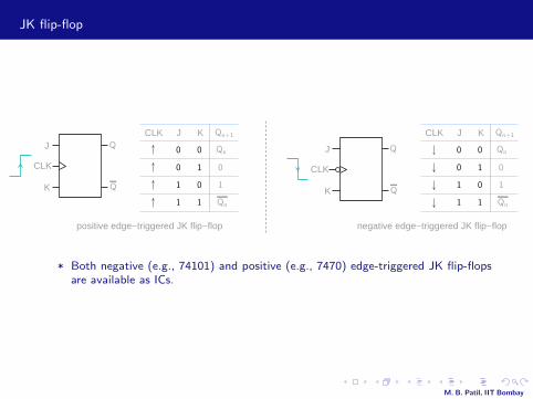
* Both negative (e.g., 74101) and positive (e.g., 7470) edge-triggered JK flip-flopsare available as ICs.
M. B. Patil, IIT Bombay
JK flip-flop
CLK
J
K
CLK KJ
positive edge−triggered JK flip−flop
CLK
J
K
CLK KJ
negative edge−triggered JK flip−flop
Q
Q 0 0
0 1
1 0
1 1
Qn
0
1
Qn
0 0
0 1
1 0
1 1
Qn
0
1
Qn
Qn+1
Q
Q
Qn+1
* Both negative (e.g., 74101) and positive (e.g., 7470) edge-triggered JK flip-flopsare available as ICs.
M. B. Patil, IIT Bombay
JK flip-flop
K
J
Master SlaveQ1
Q1
Q
Q
CLKCLK
CLK
t2Bt2At1Bt1A
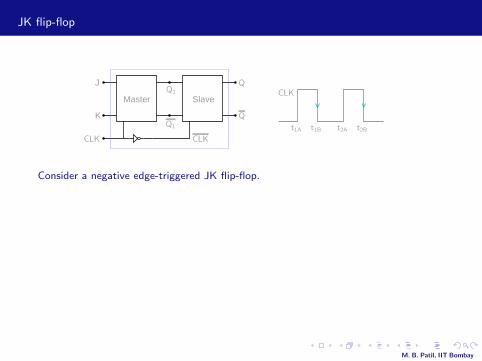
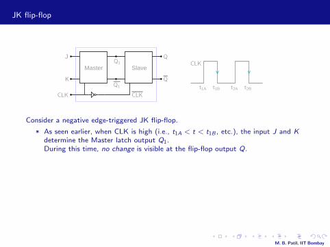
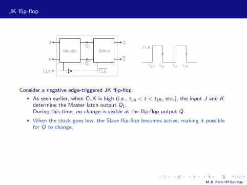
Consider a negative edge-triggered JK flip-flop.
* As seen earlier, when CLK is high (i.e., t1A < t < t1B , etc.), the input J and Kdetermine the Master latch output Q1.During this time, no change is visible at the flip-flop output Q.
* When the clock goes low, the Slave flip-flop becomes active, making it possiblefor Q to change.
* In short, although the flip-flop output Q can only change after the active edge,(t1B , t2B , etc.), the new Q value is determined by J and K values just before theactive edge.This is a very important point!
M. B. Patil, IIT Bombay
JK flip-flop
K
J
Master SlaveQ1
Q1
Q
Q
CLKCLK
CLK
t2Bt2At1Bt1A
Consider a negative edge-triggered JK flip-flop.
* As seen earlier, when CLK is high (i.e., t1A < t < t1B , etc.), the input J and Kdetermine the Master latch output Q1.During this time, no change is visible at the flip-flop output Q.
* When the clock goes low, the Slave flip-flop becomes active, making it possiblefor Q to change.
* In short, although the flip-flop output Q can only change after the active edge,(t1B , t2B , etc.), the new Q value is determined by J and K values just before theactive edge.This is a very important point!
M. B. Patil, IIT Bombay
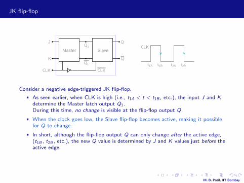
JK flip-flop
K
J
Master SlaveQ1
Q1
Q
Q
CLKCLK
CLK
t2Bt2At1Bt1A
Consider a negative edge-triggered JK flip-flop.
* As seen earlier, when CLK is high (i.e., t1A < t < t1B , etc.), the input J and Kdetermine the Master latch output Q1.During this time, no change is visible at the flip-flop output Q.
* When the clock goes low, the Slave flip-flop becomes active, making it possiblefor Q to change.
* In short, although the flip-flop output Q can only change after the active edge,(t1B , t2B , etc.), the new Q value is determined by J and K values just before theactive edge.
This is a very important point!
M. B. Patil, IIT Bombay
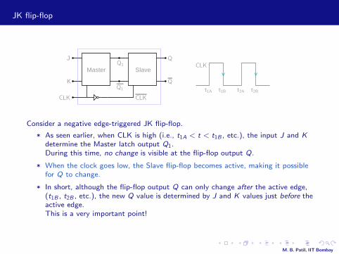
JK flip-flop
K
J
Master SlaveQ1
Q1
Q
Q
CLKCLK
CLK
t2Bt2At1Bt1A
Consider a negative edge-triggered JK flip-flop.
* As seen earlier, when CLK is high (i.e., t1A < t < t1B , etc.), the input J and Kdetermine the Master latch output Q1.During this time, no change is visible at the flip-flop output Q.
* When the clock goes low, the Slave flip-flop becomes active, making it possiblefor Q to change.
* In short, although the flip-flop output Q can only change after the active edge,(t1B , t2B , etc.), the new Q value is determined by J and K values just before theactive edge.This is a very important point!
M. B. Patil, IIT Bombay
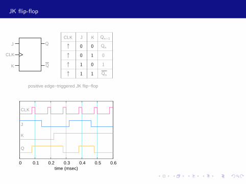
JK flip-flop
CLK J K
positive edge−triggered JK flip−flop
J
CLK
K
CLK
J
K
Q
0time (msec)
0.1 0.2 0.3 0.4 0.5 0.6
Q
Q 0 0
0 1
1 0
1 1
Qn
0
1
Qn
Qn+1
CLK J K
negative edge−triggered JK flip−flop
J
CLK
K
CLK
J
K
Q
0time (msec)
0.1 0.2 0.3 0.4 0.5 0.6
0 0
0 1
1 0
1 1
Qn
0
1
Qn
Qn+1
Q
Q
M. B. Patil, IIT Bombay
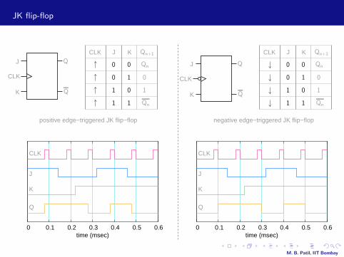
JK flip-flop
CLK J K
positive edge−triggered JK flip−flop
J
CLK
K
CLK
J
K
Q
0time (msec)
0.1 0.2 0.3 0.4 0.5 0.6
Q
Q 0 0
0 1
1 0
1 1
Qn
0
1
Qn
Qn+1 CLK J K
negative edge−triggered JK flip−flop
J
CLK
K
CLK
J
K
Q
0time (msec)
0.1 0.2 0.3 0.4 0.5 0.6
0 0
0 1
1 0
1 1
Qn
0
1
Qn
Qn+1
Q
Q
M. B. Patil, IIT Bombay
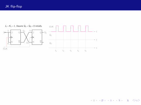
JK flip-flop
J
K
1 J
K
CLK
CLK
t
t
t
K2
J2
K1
J1Q2
Q2
Q1
t5t4t3t2t1
Q1
Q
Q
Q
Q
J1 = K1 = 1. Assume Q1 = Q2 = 0 initially.
t Q2 (t = t+k )K2 (t = t−k )J2 (t = t−k )
t1
t2
t3
t4
t5
1 10
0 01
1 0
0 0
1
1
1 10
* Since J1 = K1 = 1, Q1 toggles after every active clock edge.
* J2 = Q1, K2 = Q1. We need to look at J2 and K2 values just before the active edge, todetermine the next value of Q2.
* It is convenient to construct a table listing J2 and K2 to figure out the next Q2 value.
* Note that the circuit is not doing much, apart from taxing our minds!But hold on, some useful circuits will appear soon.
M. B. Patil, IIT Bombay
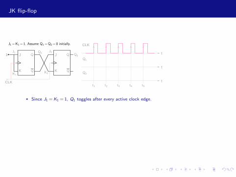
JK flip-flop
J
K
1 J
K
CLK
CLK
t
t
t
K2
J2
K1
J1Q2
Q2
Q1
t5t4t3t2t1
Q1
Q
Q
Q
Q
J1 = K1 = 1. Assume Q1 = Q2 = 0 initially.
t Q2 (t = t+k )K2 (t = t−k )J2 (t = t−k )
t1
t2
t3
t4
t5
1 10
0 01
1 0
0 0
1
1
1 10
* Since J1 = K1 = 1, Q1 toggles after every active clock edge.
* J2 = Q1, K2 = Q1. We need to look at J2 and K2 values just before the active edge, todetermine the next value of Q2.
* It is convenient to construct a table listing J2 and K2 to figure out the next Q2 value.
* Note that the circuit is not doing much, apart from taxing our minds!But hold on, some useful circuits will appear soon.
M. B. Patil, IIT Bombay
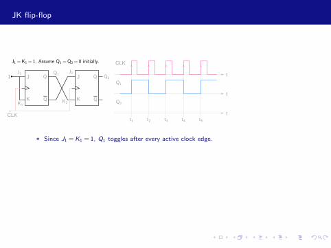
JK flip-flop
J
K
1 J
K
CLK
CLK
t
t
t
K2
J2
K1
J1Q2
Q2
Q1
t5t4t3t2t1
Q1
Q
Q
Q
Q
J1 = K1 = 1. Assume Q1 = Q2 = 0 initially.
t Q2 (t = t+k )K2 (t = t−k )J2 (t = t−k )
t1
t2
t3
t4
t5
1 10
0 01
1 0
0 0
1
1
1 10
* Since J1 = K1 = 1, Q1 toggles after every active clock edge.
* J2 = Q1, K2 = Q1. We need to look at J2 and K2 values just before the active edge, todetermine the next value of Q2.
* It is convenient to construct a table listing J2 and K2 to figure out the next Q2 value.
* Note that the circuit is not doing much, apart from taxing our minds!But hold on, some useful circuits will appear soon.
M. B. Patil, IIT Bombay
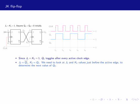
JK flip-flop
J
K
1 J
K
CLK
CLK
t
t
t
K2
J2
K1
J1Q2
Q2
Q1
t5t4t3t2t1
Q1
Q
Q
Q
Q
J1 = K1 = 1. Assume Q1 = Q2 = 0 initially.
t Q2 (t = t+k )K2 (t = t−k )J2 (t = t−k )
t1
t2
t3
t4
t5
1 10
0 01
1 0
0 0
1
1
1 10
* Since J1 = K1 = 1, Q1 toggles after every active clock edge.
* J2 = Q1, K2 = Q1. We need to look at J2 and K2 values just before the active edge, todetermine the next value of Q2.
* It is convenient to construct a table listing J2 and K2 to figure out the next Q2 value.
* Note that the circuit is not doing much, apart from taxing our minds!But hold on, some useful circuits will appear soon.
M. B. Patil, IIT Bombay
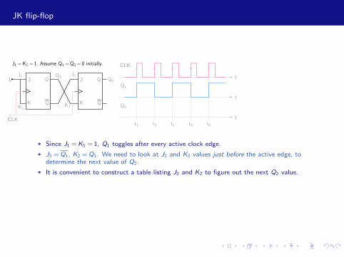
JK flip-flop
J
K
1 J
K
CLK
CLK
t
t
t
K2
J2
K1
J1Q2
Q2
Q1
t5t4t3t2t1
Q1
Q
Q
Q
Q
J1 = K1 = 1. Assume Q1 = Q2 = 0 initially.
t Q2 (t = t+k )K2 (t = t−k )J2 (t = t−k )
t1
t2
t3
t4
t5
1 10
0 01
1 0
0 0
1
1
1 10
* Since J1 = K1 = 1, Q1 toggles after every active clock edge.
* J2 = Q1, K2 = Q1. We need to look at J2 and K2 values just before the active edge, todetermine the next value of Q2.
* It is convenient to construct a table listing J2 and K2 to figure out the next Q2 value.
* Note that the circuit is not doing much, apart from taxing our minds!But hold on, some useful circuits will appear soon.
M. B. Patil, IIT Bombay
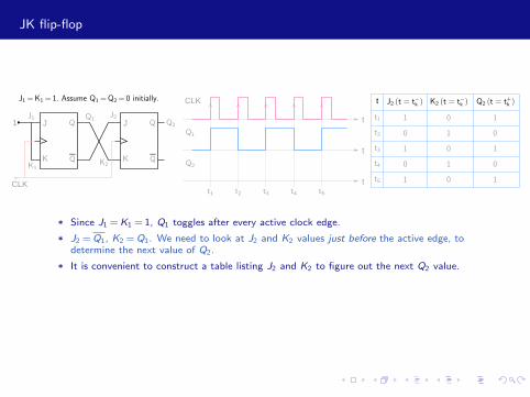
JK flip-flop
J
K
1 J
K
CLK
CLK
t
t
t
K2
J2
K1
J1Q2
Q2
Q1
t5t4t3t2t1
Q1
Q
Q
Q
Q
J1 = K1 = 1. Assume Q1 = Q2 = 0 initially. t Q2 (t = t+k )K2 (t = t−k )J2 (t = t−k )
t1
t2
t3
t4
t5
1 10
0 01
1 0
0 0
1
1
1 10
* Since J1 = K1 = 1, Q1 toggles after every active clock edge.
* J2 = Q1, K2 = Q1. We need to look at J2 and K2 values just before the active edge, todetermine the next value of Q2.
* It is convenient to construct a table listing J2 and K2 to figure out the next Q2 value.
* Note that the circuit is not doing much, apart from taxing our minds!But hold on, some useful circuits will appear soon.
M. B. Patil, IIT Bombay
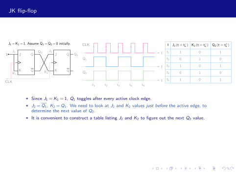
JK flip-flop
J
K
1 J
K
CLK
CLK
t
t
t
K2
J2
K1
J1Q2
Q2
Q1
t5t4t3t2t1
Q1
Q
Q
Q
Q
J1 = K1 = 1. Assume Q1 = Q2 = 0 initially. t Q2 (t = t+k )K2 (t = t−k )J2 (t = t−k )
t1
t2
t3
t4
t5
1 10
0 01
1 0
0 0
1
1
1 10
* Since J1 = K1 = 1, Q1 toggles after every active clock edge.
* J2 = Q1, K2 = Q1. We need to look at J2 and K2 values just before the active edge, todetermine the next value of Q2.
* It is convenient to construct a table listing J2 and K2 to figure out the next Q2 value.
* Note that the circuit is not doing much, apart from taxing our minds!But hold on, some useful circuits will appear soon.
M. B. Patil, IIT Bombay
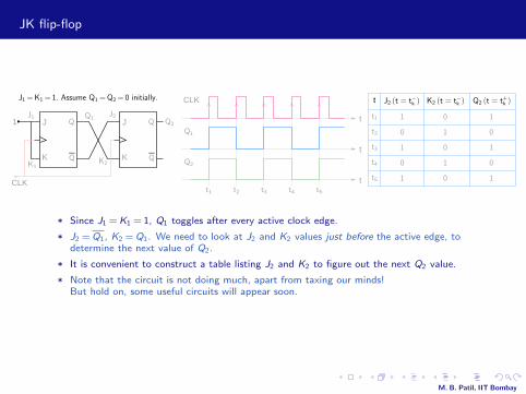
JK flip-flop
J
K
1 J
K
CLK
CLK
t
t
t
K2
J2
K1
J1Q2
Q2
Q1
t5t4t3t2t1
Q1
Q
Q
Q
Q
J1 = K1 = 1. Assume Q1 = Q2 = 0 initially. t Q2 (t = t+k )K2 (t = t−k )J2 (t = t−k )
t1
t2
t3
t4
t5
1 10
0 01
1 0
0 0
1
1
1 10
* Since J1 = K1 = 1, Q1 toggles after every active clock edge.
* J2 = Q1, K2 = Q1. We need to look at J2 and K2 values just before the active edge, todetermine the next value of Q2.
* It is convenient to construct a table listing J2 and K2 to figure out the next Q2 value.
* Note that the circuit is not doing much, apart from taxing our minds!But hold on, some useful circuits will appear soon.
M. B. Patil, IIT Bombay


