domain structures in epitaxial ferroelectric thin films
TRANSCRIPT

1
Domain Structures in Epitaxial Ferroelectric
Thin Films
By: Brian Smith
S1711377
Supervised by: Prof. dr. Beatrix Noheda
February 2009

2
TABLE OF CONTENTS
Introduction………………………………………………………………………………. 3
1. Background…………………………………………………………………………… 4
2. Experimental………………………………………………………………………….. 5
2.1. Substrate Study…………………………………………………………………... 5
2.2. Thickness Study…………………………………………………………………. 9
2.3. Cooling rate Study……………………………………………………………….. 14
3. Theoretical……………………………………………………………………………. 16
3.1. Phenomenological ……………………………………………………………….. 16
3.2. First principles: Models………………………………………………………….. 17
3.3. First principles: Thickness study………………………………………………… 26
4. Future work………………………………………………………………………….... 30
Conclusions………………………………………………………………………………. 32
Appendix A………………………………………………………………………………… 33
References………………………………………………………………………………... 34
3
Introduction
Ferroelectric materials play an essential role in modern technology. Applications of
thin film ferroelectrics include nonvolatile memories, microelectronics, electro-optics, and
electromechanical systems [1]. Development of ferroelectric thin films began in the late
1960’s for use as nonvolatile memories. Despite the promise of these thin films, research was
stifled by difficulties processing and integrated ferroelectric films. As a result little progress
was made until the 1980’s [2]. At this time improvements in processing of thin film
ferroelectric oxides allowed high quality films to be grown for research and applications.
The properties of a ferroelectric film depend greatly on the structure of the domains in
the film. The domain structure will have a great impact on the dielectric, piezoelectric and
optical properties of the film [2]. In order to obtain the optimal properties for specific
applications it is necessary to control the domain structure in the film. Different applications
of ferroelectric thin films take advantage of different properties of the film. As a result the
desired domain structures will vary depending on the application. For example, ferroelectric
films used in nonvolatile memories need to have high remnant polarization which is achieved
by domains with out of plane polarization. Conversely, domains with polarization in the
plane of the film are desired for use as capacitor devices where this domain structure increases
the dielectric constant of the film [1].
Controlling the domain structure of epitaxial ferroelectric thin films is vital if such
films are to continue to play an important role in practical applications. This paper will
examine how different parameters during film growth influence the domain structure in
ferroelectric thin films as well as determine what aspects future research must address to
continue to make meaningful progress.

4
1. Background
A ferroelectric crystal is characterized by having a spontaneous polarization in the
absence of an electric field below a transition temperature Tc. The spontaneous polarization is
the result of a shift in the centrosymmetric position of the atoms in unit cell of the crystal.
The atomic shift is very small, on the order of 0.1 Å and is usually coupled with an elongation
of the unit cell along the polar axis of the crystal [3].
The spontaneous polarization of a ferroelectric crystal in the absence of an electric
field is be oriented in various directions. Regions of the crystal in which the spontaneous
polarization are oriented in the same direction are known as ferroelectric domains. Different
domains are separated by domain walls [1]. Domain walls are characterized by the
approximate angle by which the polarization rotates between the two domains [2]. In
epitaxial ferroelectric thin films 180° and 90° domain walls are present. For 90° domain
walls the rotation of the polarization must be accompanied by a rotation in the strain, or
elongation, across the wall [3]. As a result the 90° domain wall is ferroelectric and
ferroelastic. A 180° domain does not have a rotation of the strain across the wall and is only
ferroelectric in character [3].
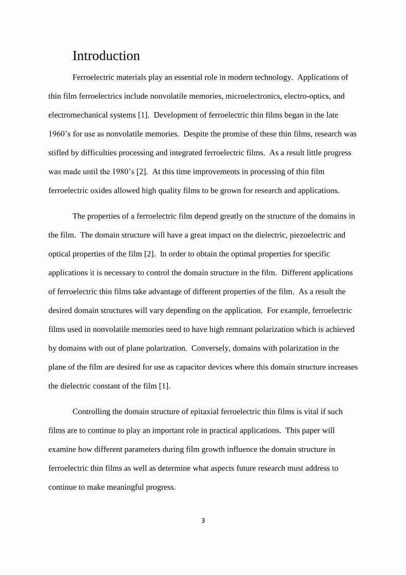
For a tetragonal ferroelectric film on a cubic substrate three different domain
structures are possible. A domain in which the c axis of the tetragonal film is aligned normal
to the film/substrate interface is known as a c domain [4]. Similarly a domain in which the c
axis of the tetragonal film is aligned parallel to the film/substrate interface is known as an a
domain [4]. An a domain can have two different orientations a1 or a2, the difference being
one is rotated 90° from the other [1]. The three domain orientations for a tetragonal film on a
cubic lattice are schematically depicted in Figure 1 [4].
5
Figure 1. Domain orientations of an epitaxial tetragonal ferroelectric with
lattice constants a and c on the [001] face of a cubic substrate with lattice
constant b. [4]
The difference between an epitaxial film and a free film is that the former is strained
so the lattice parameter of the film matches the lattice parameter of substrate. A free film, on
the other hand, is not strained [2]. Coherency is maintained between the film and substrate at
the expense of strain in the film. This strain is known as misfit strain [1]. In addition to
misfit strain there are two more sources of strain; thermal strain and transformational strain.
Thermal strain is caused by the substrate and film having different thermal expansions
coefficients. Ferroelectric films are grown at high temperatures above Tc. As the film cools
the film and substrate contract by different amounts, creating strain in the film [5].
Transformational strain occurs when the film is cooled below Tc. At this point the elongation
of the unit cell occurs adding additional strain in the film [5].
Domain structures occur to minimize the strain and electrostatic energy of the film [4].
Strain in the film can be relaxed by the formation of 90° ferroelastic domains. Since 180°
domain walls are not ferroelastic, strain relaxation cannot take place in this way [1]. In
addition to domain formation, strain relaxation can occur by the formation of misfit
dislocation. This mechanism is especially important above the transition temperature where
domains cannot form [6].

6
2. Experimental Results
The domain structure of an epitaxial ferroelectric film is determined by the conditions
in which the film is grown. There are several methods for growing ferroelectric thin films.
The two most common techniques are pulsed laser deposition (PLD) and molecular beam
epitaxy (MBE) [1]. Although each growth technique has different control parameters, there
are several parameters common to all growth techniques which determine the domain
structure of the film. This paper will examine the effect of substrate choice, film thickness,
and cooling rate on the domain structure.
2.1 Substrate Study
There are many substrates available for epitaxial growth of thin film ferroelectrics.
The ferroelectric domain structures of PbTiO3 have been investigated extensively on MgO,
SrTiO3, and KTaO3 [5] [7] [8] [9]. The different cubic lattice constants of the substrates
result in a different misfit strain in the film. These strains range from large tensile (MgO) to
small tensile (KTaO3) to small compressive (SrTiO3) strain. Examination of similar films
grown on each substrate provides information about the lattice misfit strain in the film
influences the domain structure. Table 1 summarizes the structural parameters of the film and
different substrates [5].
Material Crystal
Structure
Lattice Constant
(Å)
Misfit Strain
(x10-2
)
Thermal Expansion
Coefficient (x10-6
/K)
PbTiO3 Tetragonal c= 4.153,
a= 3.9775
NA 12.6
MgO Cubic a= 4.2551 6.524 14.8
SrTiO3 Cubic a= 3.9358 -1.05 11.7
KTaO3 Cubic a= 4.0069 .735 6.67 Table 1. Structural parameters, thermal expansion coefficients and misfit strain of various
materials at the growth temperature [5]

7
In situ synchrotron analysis has been performed on 200 nm thick PbTiO3 films grown
on MgO, SrTiO3, and KTaO3 by pulsed laser deposition. The X-ray diffraction (XRD) data
was used to determine the c domain abundance (α) of the different films [5].
The XRD analysis revealed that the domain structure of PbTiO3 on MgO consists of a
predominantly c domain structure (α~75%). Cross sectional TEM of the film, Figure 2a,
confirms that the domain structure is made up of a large percentage of c domains with small a
domains [5]. PbTiO3 films grown on SrTiO3 produced uniform c domains (α=100%). The
lack of a domains is seen in the TEM image, Figure 2b [5]. The most complicated domain
structure was observed on PbTiO3 films on KTaO3. XRD analysis reveals that the film
consists of mostly a domains (α~30%). Cross sectional TEM, Figure 2c [5], shows thin c
domains within an a domain matrix. However, plane-view TEM, Figure 2d [5], reveals a
more interesting domain structure. The a domain regions are not uniform but consist of
alternating a1 and a2 domains. The a/c and a1/a2 domain walls can be differentiated by the
direction in which they lie.
Figure 2. Cross-sectional TEM image of the PbTiO3 films grown on the (a) MgO substrate. (b)SrTiO3 substrate
(c) KtaO3 substrate, and (d) Plane-view TEM image of epitaxial PbTiO3 on the KTaO3 [5]

8
The domain structure in each film can be qualitatively explained by examining the
misfit strain and the thermal strain in the film. Adding the thermal strain from cooling at the
growth temperature (Tg) to Tc and the misfit strain gives the net strain in the film at Tc. It is
important to account for the thermal strain. Although MgO has a larger misfit strain than
KTaO3 , a film grown on the latter substrate has a larger net strain at Tc due to the large
difference in the thermal expansion coefficient between the film and substrate [5]. A plot of α
versus net strain is shown in Figure 3 [5]. It is clearly seen from this figure that α is inversely
related to the net strain.
Figure 3. Variation of c-domain abundance as a function of net elastic
strain stored in the film [Lee 2001]
To fully grasp how the strain effects the domain structure it is useful to consider three
cases; when the substrate is causing a large compressive strain, a large tensile strain, and an
intermediate situation where there is only a weak compressive or tensile strain. In the first
case, large compressive strain, the film grows c domains which minimize the stress since this
domain has the smaller lattice parameter. The opposite is true when there is a large tensile
strain. The film grows a domains where the longer lattice parameter is in the plane of the
film. The result is an alternating a1/a2 domain structure. In the intermediate case some of the
9
misfit strain can be relaxed by incorporating a small amount of the a or c domain in a large
amount of the other domain.
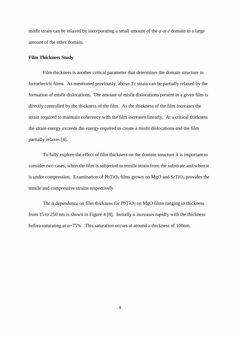
Film Thickness Study
Film thickness is another critical parameter that determines the domain structure in
ferroelectric films. As mentioned previously, above Tc strain can be partially relaxed by the
formation of misfit dislocations. The amount of misfit dislocations present in a given film is
directly controlled by the thickness of the film. As the thickness of the film increases the
strain required to maintain coherency with the film increases linearly. At a critical thickness
the strain energy exceeds the energy required to create a misfit dislocations and the film
partially relaxes [4].
To fully explore the effect of film thickness on the domain structure it is important to
consider two cases, when the film is subjected to tensile strain from the substrate and when it
is under compression. Examination of PbTiO3 films grown on MgO and SrTiO3 provides the
tensile and compressive strains respectively.
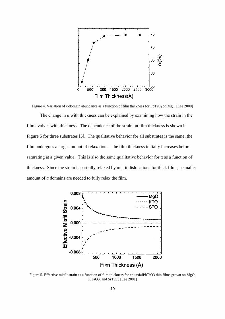
The α dependence on film thickness for PbTiO3 on MgO films ranging in thickness
from 15 to 250 nm is shown in Figure 4 [8]. Initially α increases rapidly with the thickness
before saturating at α~75% . This saturation occurs at around a thickness of 100nm.
10
Figure 4. Variation of c-domain abundance as a function of film thickness for PbTiO3 on MgO [Lee 2000]
The change in α with thickness can be explained by examining how the strain in the
film evolves with thickness. The dependence of the strain on film thickness is shown in
Figure 5 for three substrates [5]. The qualitative behavior for all substrates is the same; the
film undergoes a large amount of relaxation as the film thickness initially increases before
saturating at a given value. This is also the same qualitative behavior for α as a function of
thickness. Since the strain is partially relaxed by misfit dislocations for thick films, a smaller
amount of a domains are needed to fully relax the film.
Figure 5. Effective misfit strain as a function of film thickness for epitaxialPbTiO3 thin films grown on MgO,
KTaO3, and SrTiO3 [Lee 2001]
11
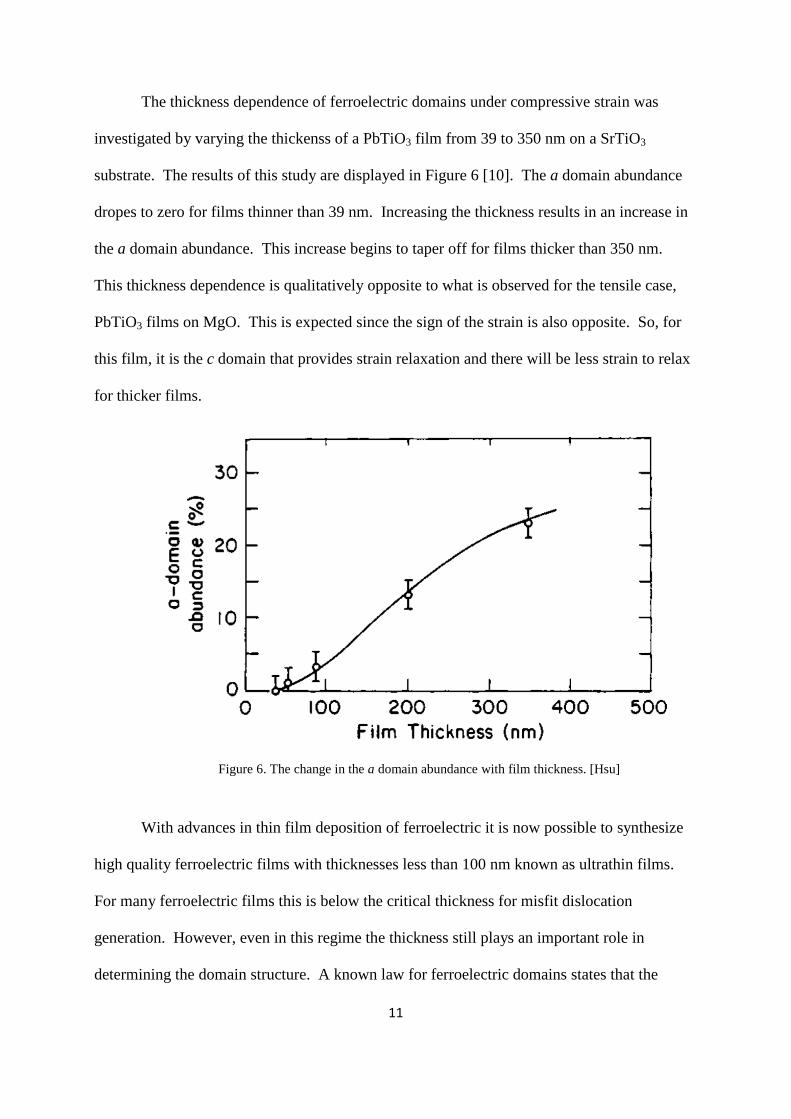
The thickness dependence of ferroelectric domains under compressive strain was
investigated by varying the thickenss of a PbTiO3 film from 39 to 350 nm on a SrTiO3
substrate. The results of this study are displayed in Figure 6 [10]. The a domain abundance
dropes to zero for films thinner than 39 nm. Increasing the thickness results in an increase in
the a domain abundance. This increase begins to taper off for films thicker than 350 nm.
This thickness dependence is qualitatively opposite to what is observed for the tensile case,
PbTiO3 films on MgO. This is expected since the sign of the strain is also opposite. So, for
this film, it is the c domain that provides strain relaxation and there will be less strain to relax
for thicker films.
Figure 6. The change in the a domain abundance with film thickness. [Hsu]
With advances in thin film deposition of ferroelectric it is now possible to synthesize
high quality ferroelectric films with thicknesses less than 100 nm known as ultrathin films.
For many ferroelectric films this is below the critical thickness for misfit dislocation
generation. However, even in this regime the thickness still plays an important role in
determining the domain structure. A known law for ferroelectric domains states that the
12
width of the domains is directly proportional to the square root of the thickness. This law,
known as Roytburd’s Law [11], has been shown to hold true for increasingly thin ferroelectric
film but is there a critical thickness below which this law breaks down? With the ability to
examine ultra thin films it is now possible to study this question experimentally. To fully
address this question both 90° and 180° domain structures will be examined to determine if,
when, and why Roytburd’s Law breaks down.
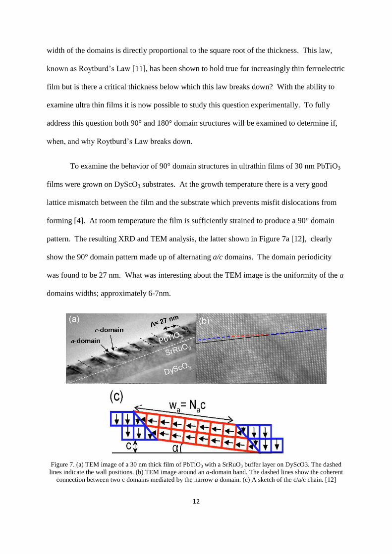
To examine the behavior of 90° domain structures in ultrathin films of 30 nm PbTiO3
films were grown on DyScO3 substrates. At the growth temperature there is a very good
lattice mismatch between the film and the substrate which prevents misfit dislocations from
forming [4]. At room temperature the film is sufficiently strained to produce a 90° domain
pattern. The resulting XRD and TEM analysis, the latter shown in Figure 7a [12], clearly
show the 90° domain pattern made up of alternating a/c domains. The domain periodicity
was found to be 27 nm. What was interesting about the TEM image is the uniformity of the a
domains widths; approximately 6-7nm.
Figure 7. (a) TEM image of a 30 nm thick film of PbTiO3 with a SrRuO3 buffer layer on DyScO3. The dashed
lines indicate the wall positions. (b) TEM image around an a-domain band. The dashed lines show the coherent
connection between two c domains mediated by the narrow a domain. (c) A sketch of the c/a/c chain. [12]
13
To understand why this occurs as well as determine a critical thickness for Roytburd’s
Law it is important to understand the origin of 90° domain walls. In order for the film to
create a 90° domain wall twinning, must occur in which the body diagonal of a unit cell on
the domain wall is shared by each domain [12]. As seen in the high resolution TEM in Figure
7b and schematically in Figure 7c [12], twining introduces a small deviation from the 90°
rotation of the polarization. The deviation is defined by the tilt angle α. As a result of tilt
angle the a domains cannot have any arbitrary width. The widths of the a domains have to be
appropriately sized so that direction of polarization of neighboring c domains remains
coherent. This introduces a minimum possible width of the a domains defined as
wamin
=c/sin(α). For PbTiO3, wamin
~6.2 nm [12]. As a result, the domain periodicity observed
is the smallest possible for a 90° domain structure in a PbTiO3 film representing a critical
thickness below which Roytburd’s Law no longer applies.
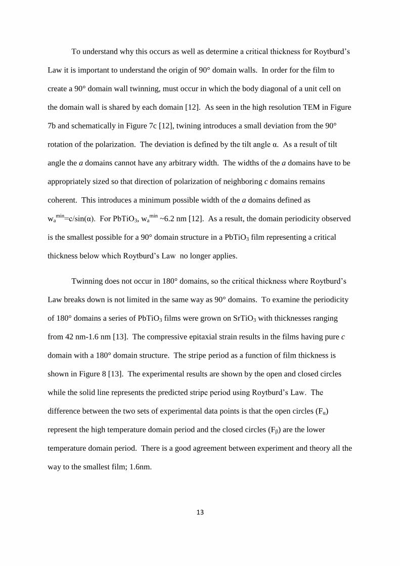
Twinning does not occur in 180° domains, so the critical thickness where Roytburd’s
Law breaks down is not limited in the same way as 90° domains. To examine the periodicity
of 180° domains a series of PbTiO3 films were grown on SrTiO3 with thicknesses ranging
from 42 nm-1.6 nm [13]. The compressive epitaxial strain results in the films having pure c
domain with a 180° domain structure. The stripe period as a function of film thickness is
shown in Figure 8 [13]. The experimental results are shown by the open and closed circles
while the solid line represents the predicted stripe period using Roytburd’s Law. The
difference between the two sets of experimental data points is that the open circles (Fα)
represent the high temperature domain period and the closed circles (Fβ) are the lower
temperature domain period. There is a good agreement between experiment and theory all the
way to the smallest film; 1.6nm.

14
Figure 8. Stripe period vs. thickness, circles represent experiment the solid line represents theory. [13]
It is clear that Roytburd’s Law holds for 180° domain in even extremely thin films.
Experimentally the critical thickness where this law breaks down has not been reached. As a
result, this limit must be explored theoretically and will be shown later.
Cooling Rate
Changing the substrate or the film thickness influences the domain structure through
the strain in the film. These two growth parameters influence a single property of the film,
the strain. There are, however, other parameters that influence the domain structure without
changing the strain in the film. One such parameter is the cooling rate after film deposition.
To investigate the effect of the cooling rate on the 90° domain structure in 400 nm
PbTiO3 films were grown on SrTiO3. These films were then subjected to three cooling rates;
slow cooling (~5°C/min), normal cooling (~30°C/min) and fast cooling (~100°C/min). Slow
and normal cooling was achieved by control of a heater attached to the substrate. For fast
cooling the sample was removed from the heater after growth and allowed to cool freely, as a
result this cooling rate is estimated [14].

15
The domain structures were analyzed using XRD to determine the volume fraction of
a domains in each sample. As the cooling rate increased, the volume fraction of the a
domains decreased. The volume fraction of the a domains for each sample is as follows; slow
cooling 15%, normal cooling 13.4%, and fast cooling 6.7% [14]. Two kinetic processes are
considered to be the cause of the domain structure dependence on the cooling rate. These two
processes are the domain nucleation and domain wall motion [14]. The paraelectric to
ferroelectric phase transition which is responsible for the creation of domain structures is a
nucleation limited process [14]. Therefore, increasing the cooling rate through this transition
limits nucleation. This causes a smaller fraction of a domains to form in films cooled
rapidly.
However, even with limited nucleation the films should still be able to relax to the
same fraction of a domains below the phase transitions, regardless of the cooling rate [1].
Apparently this is not the case. The mobility of the 90° domain walls must be impeded by
faster cooling preventing the growth of a domains to fully relax the film [1]. The precise
influence of these two effects on the domain structure remains unknown. In situ XRD
analysis of films subjected to different cooling rate would be useful in analyzing the kinetics
of 90° domain wall motion.
16
3. Theoretical Predictions
3.1 Phenomenological models
A theoretical model to predict domain structures in ferroelectric film was created by
Roytburd in the mid 1970’s [1]. This theory used a mean strain approach in involving a
summation of elastic energy and domain boundary energy. The equilibrium configurations
were determined by minimizing the summation [11]. While being relatively simple
mathematically, this theory provides a good quantitative description of domain structures in
most circumstances. The result of this theory was to predict the fraction of c domains as a
function of misfit strain and film thickness [11]. This analysis also leads to the square root
dependence of the domain period on the film thickness, Roytburd’s Law which was discussed
earlier.
Although this theory was found to provide good predictions for the domain structure
there were a number of important factors not taken into account. This theory did not address
strain relaxation from misfit dislocations. To incorporate misfit dislocations, an effective
substrate lattice parameter was introduced. This parameter changed the misfit strain in the
film used in the theory to accurately reflect strain relaxation that occurred from misfit
dislocation [6].
Even using an effective substrate lattice parameter the theory still does not accurately
predict the domain structure of the film under certain circumstances. For example, for a film
subjected to appropriate tensile strain the theory predicts that below a critical thickness a
mono-a domain structure will occur. However, it was found that an a1/a2 domain structure
was always formed [15].
17
Another theoretical approach has been developed using a Landau-Ginzburg-
Devonshire theory (16). In this theory the free energy of the system is expanded in terms of
an order parameter. For ferroelectric thin films, the polarization is often used as the order
parameter. The free energy as an expression of the order parameter is then minimized to
determine the equilibrium domain structure. This theory has been found to produce an
improvement over the mean strain approach but still does not correctly predict the domain
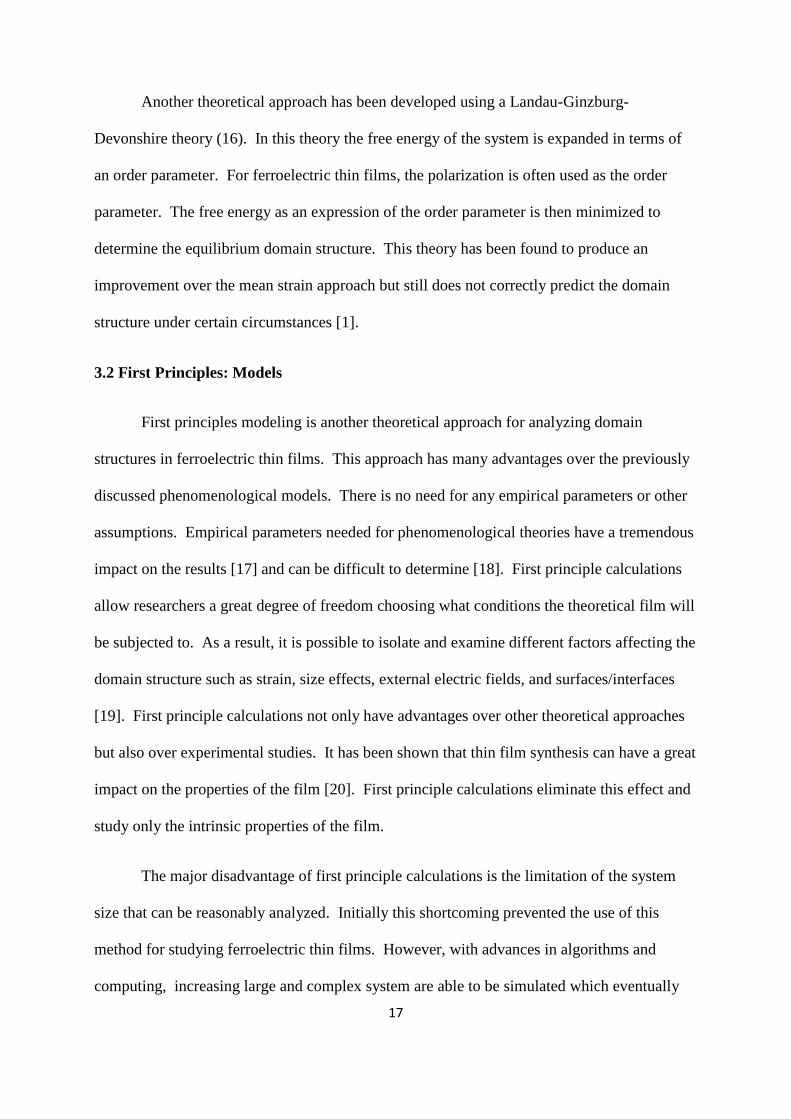
structure under certain circumstances [1].
3.2 First Principles: Models
First principles modeling is another theoretical approach for analyzing domain
structures in ferroelectric thin films. This approach has many advantages over the previously
discussed phenomenological models. There is no need for any empirical parameters or other
assumptions. Empirical parameters needed for phenomenological theories have a tremendous
impact on the results [17] and can be difficult to determine [18]. First principle calculations
allow researchers a great degree of freedom choosing what conditions the theoretical film will
be subjected to. As a result, it is possible to isolate and examine different factors affecting the
domain structure such as strain, size effects, external electric fields, and surfaces/interfaces
[19]. First principle calculations not only have advantages over other theoretical approaches
but also over experimental studies. It has been shown that thin film synthesis can have a great
impact on the properties of the film [20]. First principle calculations eliminate this effect and
study only the intrinsic properties of the film.
The major disadvantage of first principle calculations is the limitation of the system
size that can be reasonably analyzed. Initially this shortcoming prevented the use of this
method for studying ferroelectric thin films. However, with advances in algorithms and
computing, increasing large and complex system are able to be simulated which eventually

18
enabled first principle calculations to become a viable method to analyze ferroelectric thin
films [19]. It is possible to study systems of increasing size and complexity by creating non-
empirical models using parameters determined from fitting selected first principle
calculations. The size of the films that can be studied with first principle models is still
smaller than films used for technological applications. However, improvements in ultra thin
film synthesis allow a direct comparison between first principle results and experimental
observations making first principle models a valuable tool for studying ferroelectric thin
films.
The geometry used to study thin films with first principle models is a single crystalline
planar slab. First principle models require three dimensional periodicity, so the slab is
repeated periodically to produce a supercell [19]. To model a specific film, several variables
need to be defined. These variables include the orientation, number of atomic layers, and
choice of termination of the interfaces [19]. The direction of polarization is determined by the
initial structure. An epitaxial film is simulated by fixing the in-plane lattice parameters of the
film to the bulk lattice parameters of the desired substrate [21].
First principle modeling can take two forms; parameterized interatomic potentials and
effective Hamiltonians [19]. This paper will explore the construction of an effective
Hamiltonian to provide further insight in to how first principle modeling works and explore
the usefulness of such model. To begin, the effective Hamiltonian will be a function of two
quantities; the local soft mode and the strain variables [22]. Later more variables will be
added to increase the complexity and realism of the model system.
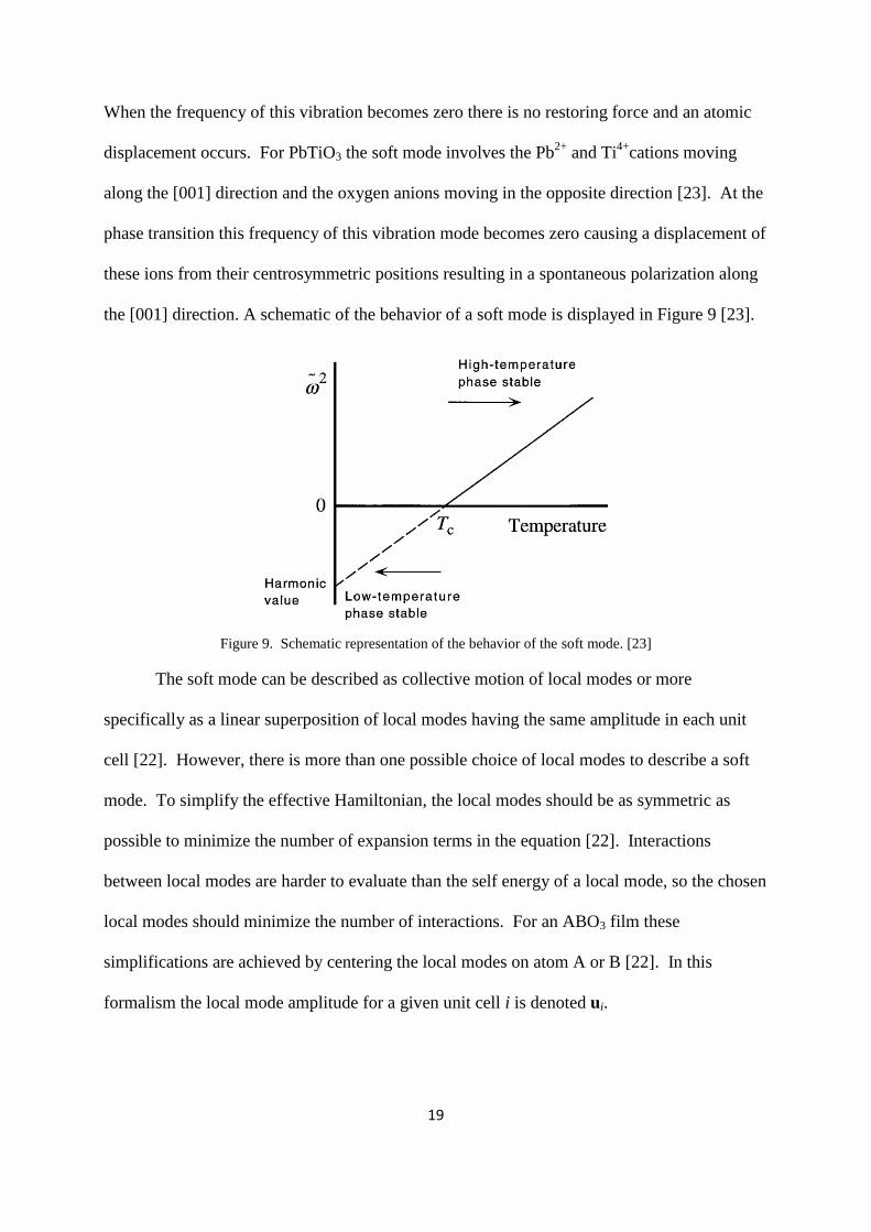
The soft mode characterizes a lattice vibration where the frequency becomes zero
upon cooling through a phase transition [23]. The vanishing frequency of this lattice vibration
corresponds to a vanishing restoring force against the deformation caused by the vibration.
19
When the frequency of this vibration becomes zero there is no restoring force and an atomic
displacement occurs. For PbTiO3 the soft mode involves the Pb2+
and Ti4+
cations moving
along the [001] direction and the oxygen anions moving in the opposite direction [23]. At the
phase transition this frequency of this vibration mode becomes zero causing a displacement of
these ions from their centrosymmetric positions resulting in a spontaneous polarization along
the [001] direction. A schematic of the behavior of a soft mode is displayed in Figure 9 [23].
Figure 9. Schematic representation of the behavior of the soft mode. [23]
The soft mode can be described as collective motion of local modes or more
specifically as a linear superposition of local modes having the same amplitude in each unit
cell [22]. However, there is more than one possible choice of local modes to describe a soft
mode. To simplify the effective Hamiltonian, the local modes should be as symmetric as
possible to minimize the number of expansion terms in the equation [22]. Interactions
between local modes are harder to evaluate than the self energy of a local mode, so the chosen
local modes should minimize the number of interactions. For an ABO3 film these
simplifications are achieved by centering the local modes on atom A or B [22]. In this
formalism the local mode amplitude for a given unit cell i is denoted ui.

20
The strain variables define the elastic deformation in the film. There are two
components to the total strain; homogeneous and inhomogeneous strain. The homogeneous
strain is the strain applied uniformly to each unit cell [22]. The effective Hamiltonian is not a
function of this type of strain. Inhomogeneous strain represents the strain of each individual
unit cell. There are six strain variables per unit cell. These six variables are not independent
and can be represented by three dimensionless displacements, vi [22]. It is these
dimensionless displacements which are varied when simulating the effective Hamiltonian.
To minimize the computational requirements of the model, two basic approximations
are made constructing the effective Hamiltonian. The first approximation is that the effective
Hamiltonian can be represented as a low order Taylor series [24]. Ferroelectric phase
transitions involve only very small atomic displacements and strain deformations. As a result,
the atomic configurations that are the most significant will be those close to the cubic
structure. So, the energy of the film can be described as a Taylor expansion of the
displacement from the cubic structure. Four terms of this expansion are needed since
ferroelectricity is an anharmonic phenomenon [24]. Higher order terms can be included to
refine the model at the expense of additional computation.
The second approximation provides the reason for the effective Hamiltonian being a
function of only the soft mode and the strain. A ferroelectric phase transition is characterized
by a decrease in the frequency of the soft mode to zero and the appearance of strain. All other
lattice vibrations are hardly affected by the transition. Describing the energy of the system
using only the soft mode and strain decreases the degrees of vibration freedom from 15 to 6,
significantly simplifying the calculations [22].
To describe the energy of the system the effective Hamiltonian consists of five parts; a
local mode self energy, a long range dipole-dipole interaction, short range interactions
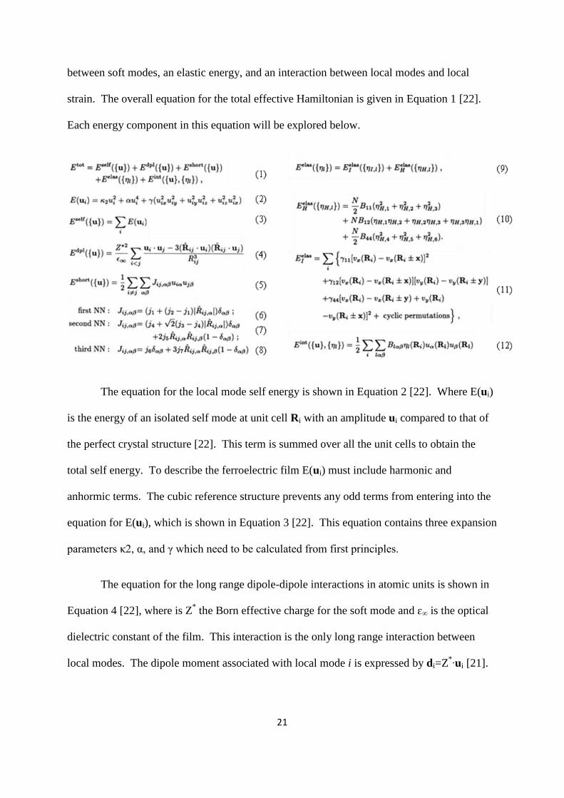
21
between soft modes, an elastic energy, and an interaction between local modes and local
strain. The overall equation for the total effective Hamiltonian is given in Equation 1 [22].
Each energy component in this equation will be explored below.
The equation for the local mode self energy is shown in Equation 2 [22]. Where E(ui)
is the energy of an isolated self mode at unit cell Ri with an amplitude ui compared to that of
the perfect crystal structure [22]. This term is summed over all the unit cells to obtain the
total self energy. To describe the ferroelectric film E(ui) must include harmonic and
anhormic terms. The cubic reference structure prevents any odd terms from entering into the
equation for E(ui), which is shown in Equation 3 [22]. This equation contains three expansion
parameters κ2, α, and γ which need to be calculated from first principles.
The equation for the long range dipole-dipole interactions in atomic units is shown in
Equation 4 [22], where is Z* the Born effective charge for the soft mode and ɛ∞ is the optical
dielectric constant of the film. This interaction is the only long range interaction between
local modes. The dipole moment associated with local mode i is expressed by di=Z*∙ui [21].

22
Short range interactions between soft modes are the result of differences of short range
repulsions and electronic hybridization between two adjacent local modes and that of two
isolated local modes. The equation for this energy contribution expanded to the second order
is displayed in Equation 5 [22]. The term Jijαβ is the coupling matrix between neighboring
local modes i and j. Since these are short range interactions Jijαβ will decrease very rapidly for
an increase in Rij. The coupling matrix can be determined for any arbitrary number of nearest
neighbors. In this example the short range interactions between three degrees of nearest
neighbors are considered. The equation between the coupling matrixes of nearest, next
nearest, and next next nearest neighbors are shown in Equations 6, 7, and 8 respectively [22].
The coefficients j1,…,j7 are the intersite interactions which can be seen schematically in
Figure 10 [22].
Figure 10. The independent intersite interaction coefficients. [22]
The elastic energy term is the sum of two energies, Equation 9 [22]. These two
energies represent the energy contribution from the homogeneous strain and the
inhomogeneous strain. The homogenous strain tensor is represented by six components ηℓ,
where ℓ=(1,…,6) using Voigt notation, see Appendix A. The homogenous strain allows the
simulated cell to vary in shape. An epitaxial film is simulated by setting η1= η2=δ and η6=0
23
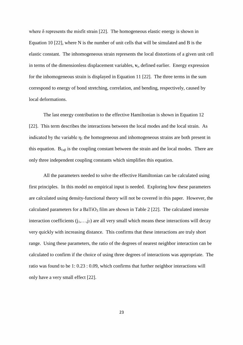
where δ represents the misfit strain [22]. The homogeneous elastic energy is shown in
Equation 10 [22], where N is the number of unit cells that will be simulated and B is the
elastic constant. The inhomogeneous strain represents the local distortions of a given unit cell
in terms of the dimensionless displacement variables, vi, defined earlier. Energy expression
for the inhomogeneous strain is displayed in Equation 11 [22]. The three terms in the sum
correspond to energy of bond stretching, correlation, and bending, respectively, caused by
local deformations.
The last energy contribution to the effective Hamiltonian is shown in Equation 12
[22]. This term describes the interactions between the local modes and the local strain. As
indicated by the variable ηℓ the homogeneous and inhomogeneous strains are both present in
this equation. Bℓαβ is the coupling constant between the strain and the local modes. There are
only three independent coupling constants which simplifies this equation.
All the parameters needed to solve the effective Hamiltonian can be calculated using
first principles. In this model no empirical input is needed. Exploring how these parameters
are calculated using density-functional theory will not be covered in this paper. However, the
calculated parameters for a BaTiO3 film are shown in Table 2 [22]. The calculated intersite
interaction coefficients (j1,…,j7) are all very small which means these interactions will decay
very quickly with increasing distance. This confirms that these interactions are truly short
range. Using these parameters, the ratio of the degrees of nearest neighbor interaction can be
calculated to confirm if the choice of using three degrees of interactions was appropriate. The
ratio was found to be 1: 0.23 : 0.09, which confirms that further neighbor interactions will
only have a very small effect [22].
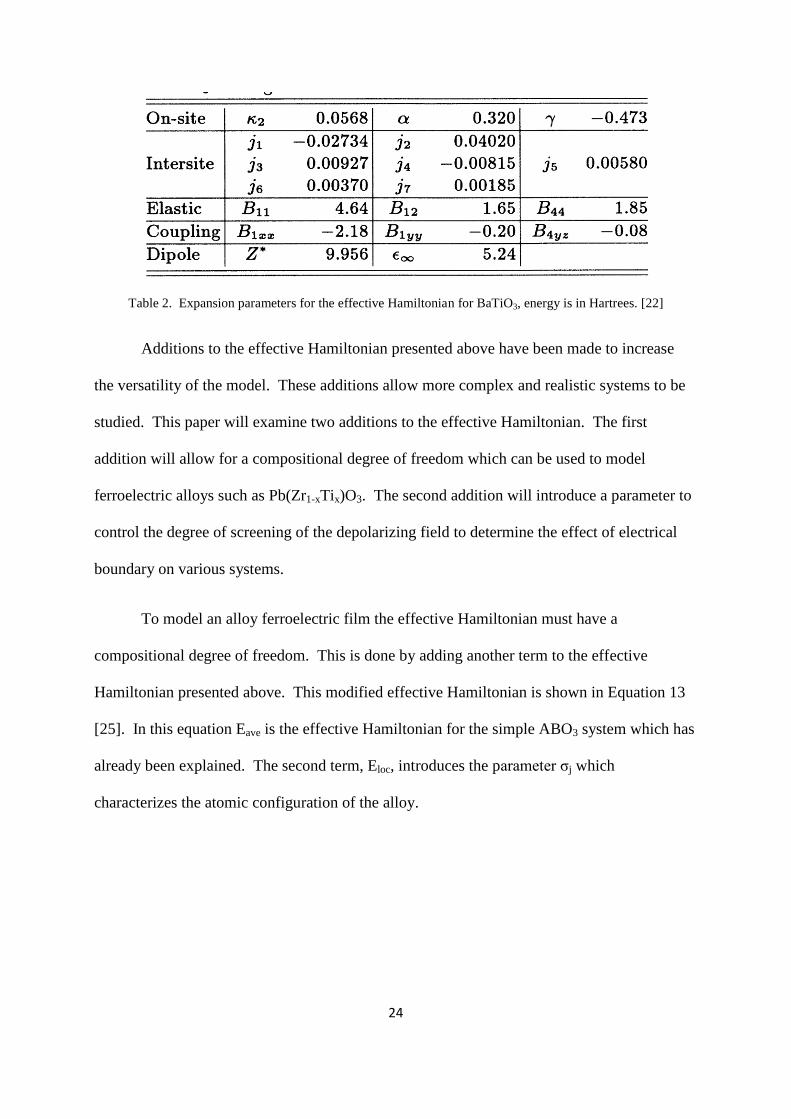
24
Table 2. Expansion parameters for the effective Hamiltonian for BaTiO3, energy is in Hartrees. [22]
Additions to the effective Hamiltonian presented above have been made to increase
the versatility of the model. These additions allow more complex and realistic systems to be
studied. This paper will examine two additions to the effective Hamiltonian. The first
addition will allow for a compositional degree of freedom which can be used to model
ferroelectric alloys such as Pb(Zr1-xTix)O3. The second addition will introduce a parameter to
control the degree of screening of the depolarizing field to determine the effect of electrical
boundary on various systems.
To model an alloy ferroelectric film the effective Hamiltonian must have a
compositional degree of freedom. This is done by adding another term to the effective
Hamiltonian presented above. This modified effective Hamiltonian is shown in Equation 13
[25]. In this equation Eave is the effective Hamiltonian for the simple ABO3 system which has
already been explained. The second term, Eloc, introduces the parameter σj which
characterizes the atomic configuration of the alloy.
25
The expressions for Eloc will account for the effect of an alloy on the self energy and
the intersite contributions. The functional form of Eloc is given in Equation 14 [25]. The first
term in this expression characterizes the onsite contribution of the alloy. This expression has
the same functional form as the self energy of a non-alloy, the only difference being the
coefficients are replaced with ∆α(σj) and ∆γ(σj). These two coefficients take into account the
contribution of the alloy.
The second term in Equation 14 represents the intersite contributions. The terms eij
and fij are unit vectors that point from site j to the origin of the local mode, ui, and
displacement, vi, respectively [25]. Once again the coefficients R(σj) and Q(σj) represent the
alloy-induced contributions to the intersite energy. The first term in the sum provides a
description of the alloy induced local mode intersite interactions. The second term in the sum
represents the effect of the alloy on the elastic intersite interactions. Higher order powers of
ui and vi can be included in this equation, but this level of detail has been found to produce a
good agreement with experimental results [25]. The compositional parameters are determined
from first principle calculations.

26
The effective Hamiltonian presented thus far only models a ferroelectric film
under open circuit conditions [26]. To model films that are not under ideal open circuit
conditions an expression is added to the effective Hamiltonian which models the effect of an
internal field in the film. This internal field arises to partially or fully screen the polarization
induced surface charges. The effective Hamiltonian to model a film under different electrical
boundary conditions is shown in Equation 15. [26]
The first term in this equation is the alloy effective Hamiltonian developed above.
The second term in the equations accounts for the internal field. The energy of the internal
field is a function of the Born effective charge, the lattice constant (a), the dielectric constant,
and the average of the z component of the local modes centered at the surfaces <uj,z>s. The
parameter β is introduced to control the strength of the internal field. An open circuit
configuration is achieved by setting β=0. Increasing β will decrease the strength of the field.
When β is large enough the energy of the internal field will disappear and the short circuit
condition is reached. The value required to reach the ideal short circuit condition will depend
on the geometry of the supercell [26].
Solving the effective Hamiltonian is achieved using a Monte Carlo simulation. This
approach is used because a Monte Carlo simulation only computes changes in the total energy
which reduces the calculations needed for the simulation [22]. During the simulations a
single variable is changed and the total energy change is then calculated. If the energy
decreases than the move is accepted. In one sweep of the simulation each ui is varied in
sequence followed by a change in each vi in sequence. When one sweep is completed the
variable being explored in the particular study is then changed and another sweep is
performed. To ensure that the system has reached its lowest possible energy state tens of
thousands of sweeps are performed [22].
27
3.3 First Principles: Thickness Study
A first principle effective Hamiltonian model is a powerful tool to study the domain
structures in ultrathin ferroelectric films. This technique has been used to explore if a critical
thickness exists below which Roytburd’s Law breaks down for 180° domains. This example
illustrates the power of using first principle models. The simulated films were
Pb(Zr0.4Pb0.6)O3 oriented in the [001] direction. These films were simulated to be under a
compressive misfit strain of -2.65% at 10 K with 80% screening of the depolarizing field.
These conditions were chosen to create 180° domains in the simulated films [21]. To
determine the critical thickness for Roytburd’s Law films of varying thickness from 1.2 nm to
14.4 nm were simulated. To perform the simulation stripe domain periods alternating along
the x direction with a chosen domain period were constructed. These domains were then
allowed to relax over a Monte Carlo simulation.
The ground state domain periodicity as a function of the square root of the film
thickness is plotted in Figure 11 [21]. Linear fit of the data points for films thicker than 2.0
nm confirm that Roytburd’s Law applies for these films. This result is in agreement with the
experimental result examined earlier. However, for the thinnest film, 1.2nm thick, no ground
state period was found. This means that for films thinner than 1.2nm Roytburd’s Law breaks
down and the domain periodicity is no longer proportional to the square root of the thickness.

28
Figure 11. Periodicity as a function of the square root of the thickness-related integer. [21]
In addition to determining the critical thickness for Roytburd’s Laws these simulations
also provide insight into the morphology of the domains when the film thickness is varied.
The total energy per unit cell of the film as a function of the domain period is displayed in
Figure 12 [21] for several film thicknesses increasing from left to right. The lowest point on
the plot corresponds to the ground state stripe domain periodicity. The other points in the plot
represent metastable stripe domain periods. These figures display an interesting trend. The
energy curves become smoother as the thickness of the film increases with more metastable
periodicities close to the energy of the ground state period. As a result, thicker films should
have domains of varying widths. It should be noted that this result has been observed
experimentally [13] [27].
Figure 12. Energy per unit cell as a function of stripe periodicity for (a) 2.0 nm (b) 5.2 nm, and (c) 10.0 nm thick
films [21]
29
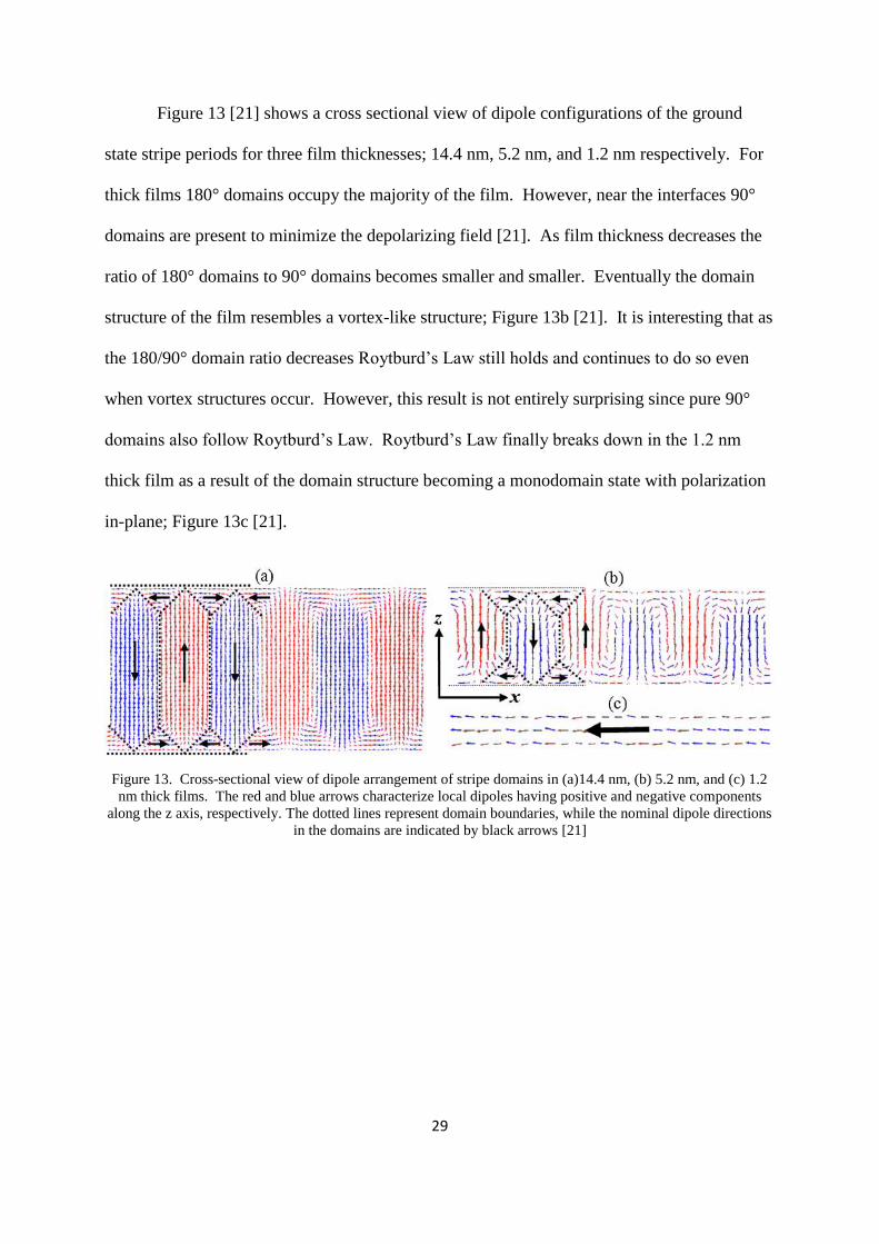
Figure 13 [21] shows a cross sectional view of dipole configurations of the ground
state stripe periods for three film thicknesses; 14.4 nm, 5.2 nm, and 1.2 nm respectively. For
thick films 180° domains occupy the majority of the film. However, near the interfaces 90°
domains are present to minimize the depolarizing field [21]. As film thickness decreases the
ratio of 180° domains to 90° domains becomes smaller and smaller. Eventually the domain
structure of the film resembles a vortex-like structure; Figure 13b [21]. It is interesting that as
the 180/90° domain ratio decreases Roytburd’s Law still holds and continues to do so even
when vortex structures occur. However, this result is not entirely surprising since pure 90°
domains also follow Roytburd’s Law. Roytburd’s Law finally breaks down in the 1.2 nm
thick film as a result of the domain structure becoming a monodomain state with polarization
in-plane; Figure 13c [21].
Figure 13. Cross-sectional view of dipole arrangement of stripe domains in (a)14.4 nm, (b) 5.2 nm, and (c) 1.2
nm thick films. The red and blue arrows characterize local dipoles having positive and negative components
along the z axis, respectively. The dotted lines represent domain boundaries, while the nominal dipole directions
in the domains are indicated by black arrows [21]

30
4. Future Work
Work on epitaxial ferroelectric thin films has made great progress in devolving a
fundamental understanding of the domain structure in these thin films. However, there are
still unanswered and half-answered questions that need to be addressed to expand the body of
knowledge in this field.
Methods for ferroelectric thin film growth need to be continually improved to allow
the synthesis and characterization of thinner films. Also, the size and complexity of model
systems that can be studied needs to be expanded. This will create a larger overlap for direct
comparison between theoretical simulations and experimental observations. Having direct
experimental observations to evaluate theoretical simulations enables theoreticians to refine
first principle models. New additions will be made to the effective Hamiltonian to increase
the realism of these models to match with experimental observations. In turn,
experimentalists will benefit as well. The refinement of first principle models will result in a
greater fundamental understanding how specific parameters influence the domain structure of
ferroelectric thin films. This fundamental understanding can then be used by experimentalists
to improve synthesis techniques to create and study new systems.
Another aspect of this field that is not fully understood is how the kinetics of domain
nucleation and growth affect the final domain structure. Experimental observations clearly
show that the cooling rate of the film to room temperature from growth temperature has a
large impact on the domain structure. Suppression of domain nucleation and obstruction of
domain wall motion have been proposed as reasons for the experimental observations.
However, the exact influence of each factor on the domain structure remains unclear. In situ
31
observation of kinetic domain processes upon cooling would prove very insightful in
examining this question.
There are a number of challenges that first principle modeling must address to analyze
more realistic systems. These challenges include the incorporation of defect effects and
external electric fields. In addition to these specific challenges for ferroelectric thin films,
first principle modeling will benefit greatly from advances in computing which will enable
larger systems to be modeled.
Interest in ferroelectric thin films is driven by the potential for creating ferroelectric
materials with enhanced material properties for technological applications. This interest must
remain high if researchers and funding will continue to be devoted to this field. Therefore,
further insight into the fundamental properties and behavior of domain structures needs to be
translated into technological applications.
32
Conclusions
The properties of ferroelectric thin films are greatly influenced by their domain
structure. As a result, control of the domain structure is vital to obtain desirable properties for
technological applications. This paper has explored what parameters critically influence
domain structures in ferroelectric thin films.
In doing so, both experimental and theoretical studies were examined to provide an
understanding of both the breadth and depth of research in this field. Specific experimental
studies highlighted how the different growth parameters influenced the domain structure.
Fundamental knowledge of ferroelectric films has enabled the creation of powerful theoretical
tools to further explore domain structures. Lastly, this paper highlighted research that must be
done to continue to make meaningful progress in understanding and controlling ferroelectric
domain structures.
33
Appendix A
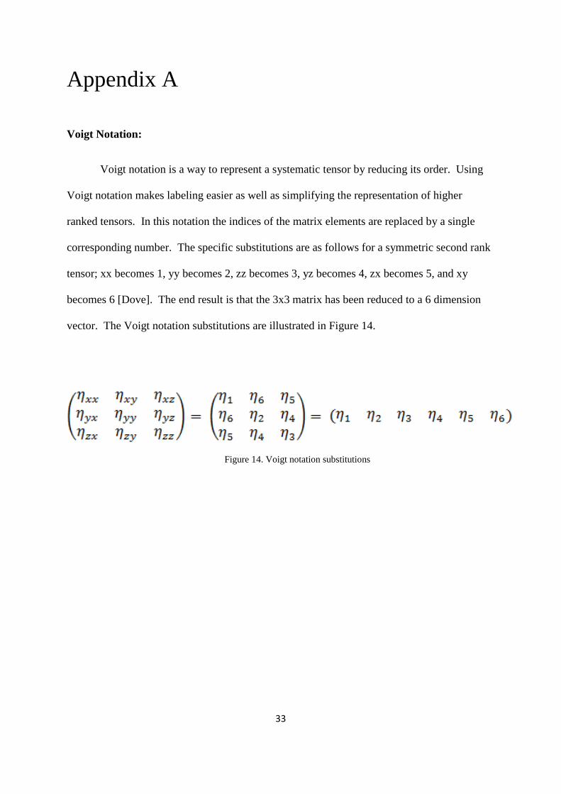
Voigt Notation:
Voigt notation is a way to represent a systematic tensor by reducing its order. Using
Voigt notation makes labeling easier as well as simplifying the representation of higher
ranked tensors. In this notation the indices of the matrix elements are replaced by a single
corresponding number. The specific substitutions are as follows for a symmetric second rank
tensor; xx becomes 1, yy becomes 2, zz becomes 3, yz becomes 4, zx becomes 5, and xy
becomes 6 [Dove]. The end result is that the 3x3 matrix has been reduced to a 6 dimension
vector. The Voigt notation substitutions are illustrated in Figure 14.
Figure 14. Voigt notation substitutions

34
References
[1] K. Lee, S. Baik, Annu. Rev. Mater. Res. 36, 81 (2006).
[2] Setter et al. J. Appl. Phys. 100, 051606 (2006).
[3] D.D. Fong, C. Thompson, Annu. Rev. Mater. Res. 36, 431 (2006).
[4] W. Pompe, X. Gong, Z. Suo, and J. S. Speck, J. Appl. Phys. 74, 6012 (1993).
[5] K. S. Lee, J. H. Choi, J. Y. Lee, and S. Baik, J. Appl. Phys. 90, 4095 (2001).
[6] J.S. Speck, W. Pomp , J. Appl. Phys. 76, 466 (1994).
[7]B.S. Kwak, A. Erbil , B.J. Wilkens, J.D. Budai, M.F. Chisholm, L.A. Boatner. Phys. Rev.
Lett. 68, 3733 (1992)
[8] K. S. Lee and S. Baik, J. Appl. Phys. 87, 8035 (2000).
[9] Z. Li, C.M. Foster, D. Guo, H. Zhang, G.R. Bai, et al. Appl. Phys. Lett. 65, 1106 (1994)
[10] W. Y. Hsu, R. Raj, Appl. Phys. Lett. 67 792 (1995).
[11] A. L. Roytburd, Phys. Status Solidi A 37, 329 (1976).
[12] A. H. G. Vlooswijk, B. Noheda, G. Catalan, A. Janssens, B. Barcones, G. Rijnders, D. H.
A. Blank, S. Venkatesan, B. Kooi, and J. T. M. de Hosson, Appl. Phys. Lett. 91, 112901
(2007).
[13] S. K. Streiffer, J. A. Eastman, D. D. Fong, C. Thompson, A. Munkholm, M. V. Ramana
Murty, O. Auciello, G. R. Bai, and G. B. Stephenson, Phys. Rev. Lett. 89, 067601
(2002).

35
[14] C.M Foster, W. Pompe ,A.C. Daykin, J.S. Speck, J. Appl. Phys. 79, 1405 (1996).
[15] A. E. Romanov, W. Pompe, and J. S. Speck, J. Appl. Phys. 79, 4037 (1996).
[16] N. A. Pertsev and A. G. Zembilgotov, J. Appl. Phys. 78, 6170 (1995).
[17] O. Dieguez, S. Tinte, A. Antons, C. Bungaro, J. B. Neaton, K. M. Rabe, D. Vanderbilt,
Phys. Rev. B 69, 212101 (2004).
[18] A. Kopal, B. Bahnik, J. Fousek, Ferroelectrics 202, 267 (1997).
[19] M. Dawber, K. M. Rabe, J. F. Scott, Reviews, Rev. Mod. Phys. 77, 1083 ( 2005).
[20 ] D. O. Klenov, T. R. Taylor, S. Stemmer, , J. Mater. Res. 19, 1477 (2004).
[21] B. Lai, I Ponomareva, I. Kornev, L. Bellaiche, and G. Salamo Appl. Phys. Lett. 91,
152909 (2007).
[22] W. Zhong, D. Vanderbilt, and K. M. Rabe Phys. Rev. B 52 6301 (1995)
[23] M. Dove, American Mineralogist 82, 213 (1997).
[24]W. Zhong, D. Vanderbilt, and K. M. Rabe, Phys. Rev. Lett. 73, 1861 (1994).
[25] L. Bellaiche, A. Garcı´a, and D. Vanderbilt, Phys. Rev. Lett. 84, 5427 (2000).
[26] I. Kornev, H. Fu, and L. Bellaiche, Phys. Rev. Lett. 93, 196104 (2004).
[27] A. Schilling, T. B. Adams, R. M. Bowman, J. M. Gregg, G. Catalan, J. F. Scott, Phys.
Rev. B 74, 024115 (2006).
[28] M. Dove, Structure and Dynamics: An Atomic View of Materials (Oxford University
Press, Oxford, 2003).