structural and electromechanical properties of epitaxial bifeo3 thin films
TRANSCRIPT

STRUCTURAL AND ELECTROMECHANICAL PROPERTIES
OF EPITAXIAL BIFEO3 THIN FILMS
by
Rebecca J. Sichel
A dissertation submitted in partial fulfillment of
the requirements for the degree of
Doctor of Philosophy
(Materials Science)
at the
UNIVERSITY OF WISCONSIN-MADISON
2011

© Copyright by Rebecca Sichel 2011
All Rights Reserved

i
Abstract
BiFeO3 has coupled ferroelectric and antiferromagnetic properties. Before this
multiferroic coupling can be exploited or even completely understood, it is necessary to
characterize the structure and electromechanical properties. We used x-ray diffraction to
study the structure of thin films of BiFeO3 on SrRuO3 conducting layers epitaxially deposited
on a SrTiO3 substrate. For 400 nm (001) oriented BiFeO3 thin films, we found a rotation of
the atomic planes in the entire film caused by anisotropic relaxation on the miscut substrate.
Mosaic blocks several microns in size had additional small, random rotations caused by the
relaxation process. Within each mosaic block we found x-ray scattering signatures of a
striped ferroelectric domain structure consistent with a strained rhombohedral phase.
Time resolved synchrotron x-ray microdiffraction was used to probe the piezoelectric
response of the film within a single mosaic block. We found that the out of plane d33
piezoelectric coefficient was uniform across the entire film (d33 = 53 pm/V). The local in-
plane response varied widely, however. We believe the variation in the apparent d31 is an
effect of differences in mechanical constraints for each ferroelectric domain. The variation
related to the proximity of the domain to a defect, dislocation, or edge of a mosaic block as
well as the neighboring polarization domains.

ii
Forbidden x-ray diffraction reflections were observed which are incompatible with the
accepted R3c symmetry of BiFeO3. These reflections were characterized to determine their
origin and improve our understanding of the structure. The intensity of the forbidden
reflections is larger in films that are relaxed, but are present in bulk crystals of BiFeO3 as
well. The pseudocubic ½(111) reflection exhibits a resonant enhancement near the Fe K-
edge on top of a non-resonant signal. The observed intensities were compared to structure
factor calculations in which Fe cations are displaced from their positions in published
structural refinements of BiFeO3. A model in which neighboring Fe cations are displaced in
antiparallel directions matches the intensities and wavevectors of the observed reflections.
Charge disproportionation induced by oxygen vacancies is a potential driving force for these
Fe displacements.

iii
Acknowledgements
Sincere and enthusiastic thanks go to my advisor, Paul Evans, for all the
encouragement, support, ideas, and patience he has given me during my graduate career. The
staff at the synchrotrons provided innumerable hours of support – Zhonghou Cai, Eric
Dufresne, Bernhard Adams, and Martin Holt at the APS, Kenneth Evans-Lutterodt at NSLS,
and Osami Sakata at SPring-8. Thanks go to Rasmi Das, Chang-Beom Eom and Sang-Wook
Cheong for providing samples. The entire Evans group has been a great help. Alexei
Grigoriev and Dal-Hyun Do helped teach me x-ray scattering; Pice Chen and Ji-Young Jo
were my fellow soldiers in the trenches during beamtime; and Soonjoo Seo was always there
to lend a friendly word of encouragement.
Most of all, I would like to thank my family. My mother- and father-in-law, Kathy
and Kevin Tissot, provided child care and hot meals which gave me time and energy to work.
My father, Dan Sichel, helped by listening to the science and by asking all the not-so-stupid
questions which were so easy to forget. My greatest supporter was my husband, Eric Tissot,
who nagged at just the right times and offered unwavering encouragement all the rest.
Writing this thesis would not have been possible without him. This thesis is dedicated to my
mother Debbie and my son William – the woman who did everything for me, and the boy
who taught me to happily do the same for him.

iv
Table of Contents
Abstract ......................................................................................................................................... i
Acknowledgements ..................................................................................................................... iii
Table of Contents ........................................................................................................................ iv
Table of Figures .......................................................................................................................... vi
Chapter 1. Motivation, Background, and Methods ...................................................................... 1
1.1. Motivation ..............................................................................................................................3
1.2. Organization of this Thesis ....................................................................................................4
1.3. Ferroelectric oxides ................................................................................................................5
1.4. The perovskite structure .........................................................................................................8
1.5. Bismuth ferrite .....................................................................................................................11
1.6. Calculating x-ray scattering intensities ................................................................................17
1.7. Experimental methods ..........................................................................................................22
1.8. Summary ..............................................................................................................................36
1.9. Chapter 1 references .............................................................................................................37
Chapter 2. Anisotropic Relaxation of Epitaxial (001) BiFeO3 Thin Films ................................ 44
2.1. Introduction ..........................................................................................................................44
2.2. Experimental methods ..........................................................................................................46
2.3. Film rotation caused by substrate miscut .............................................................................47
2.4. Mosaic block rotation ...........................................................................................................57
2.5. Strained stripe domains within mosaic blocks .....................................................................59
2.6. Conclusions ..........................................................................................................................67
2.7. Chapter 2 references .............................................................................................................68
Chapter 3. X-ray Diffraction Signatures of Ferroelectric Polarization ...................................... 71
3.1. Kinematic scattering from PbTiO3 : A qualitative prediction for PZT intensity contrast....74
3.2. Intensity contrast measurements ..........................................................................................80
3.3. Intensity contrast at 14 keV ..................................................................................................90
3.4. Resonant enhancement of intensity contrast ........................................................................91

v
3.5. Refinement of the kinematic scattering model .....................................................................94
3.6. Conclusion ............................................................................................................................99
3.7. Chapter 3 references ...........................................................................................................101
Chapter 4. Piezoelectric Response of BiFeO3 (001) Thin Films.............................................. 103
4.1. Introduction ........................................................................................................................103
4.2. Experimental methods ........................................................................................................108
4.3. Measurement of out-of-plane piezoelectric coefficient d33 ................................................113
4.4. In-plane piezoelectric response and d31 ..............................................................................116
4.5. Conclusions ........................................................................................................................123
4.6. Chapter 4 references ...........................................................................................................124
Chapter 5. Resonant and Non-Resonant Diffraction from Forbidden Reflections in BiFeO3 . 126
5.1. Predicted intensities of magnetic scattering .......................................................................127
5.2. Experimental setup .............................................................................................................129
5.3. Forbidden ½{111} reflections in thin films .......................................................................139
5.4. ½{111} reflections in bulk BiFeO3 ....................................................................................143
5.5. Response of ½{111} reflections to piezoelectric strain .....................................................149
5.6. Resonant diffraction and chemical shift of ½{111} reflections .........................................154
5.7. Structural distortion models for ½(hkl) reflections ............................................................157
5.8. Discussion ..........................................................................................................................163
5.9. Summary ............................................................................................................................165
5.10. Chapter 5 references .........................................................................................................167

vi
Table of Figures
Figure 1.1. Ferroelectric hysteresis loop schematic. ................................................................... 6
Figure 1.2. Perovskite structure ABO3.. ...................................................................................... 9
Figure 1.3. Structure of BiFeO3. ............................................................................................... 12
Figure 1.4. Definition of q, scattering angles and incident and scattered x-ray
wavevectors. .............................................................................................................................. 18
Figure 1.5. Voltage and switching current from a 100μm diameter Pb(Zr,Ti)O3
capacitor measured during a poling pulse train resulting in a Pup state. ................................... 25
Figure 1.6. Hysteresis loop of 100 µm diameter Pb(Zr,Ti)O3 capacitor at 10 kHz .................. 26
Figure 1.7. Scattering geometry angle definitions for four circle diffractometers. ................... 27
Figure 1.8. Schematic of synchrotron microdiffraction. ........................................................... 29
Figure 1.9. Chromium knife edge scan of focused x-ray beam. ............................................... 31
Figure 1.10. Schematic diagram of time resolved microdiffraction ........................................ 35
Figure 2.1. Incident angle of peak for (002) reflection as a function of azimuthal angle ......... 50
Figure 2.2. Area-averaged reciprocal space map of the BiFeO3 (002), SrRuO3 (220),
and SrTiO3 (002) at 8.05 keV ................................................................................................... 51
Figure 2.3. Step edge relaxation for a compressively strained epitaxial film. .......................... 53
Figure 2.4 Components of dislocations relaxing an epitaxial thin film on a miscut
substrate ..................................................................................................................................... 55
Figure 2.5 (a) X-ray microdiffraction image of mosaic blocks using the (002) reflection
of BiFeO3 .................................................................................................................................. 58
Figure 2.6 (a) Four structural variants of a rhombohedral ferroelectric film on a cubic
substrate. .................................................................................................................................... 60
Figure 2.7 Microdiffraction image using the BiFeO3 {103} reflections at 2θ = 50.73° at
the area marked 1. Reciprocal space maps taken at positions 1 (b) and 2 (c) on the
surface ....................................................................................................................................... 62
Figure 2.8. Three dimensional reciprocal space map of the SrTiO3, SrRuO3, and
BiFeO3 {103} reflections projected onto the (a) qx-qz plane and (b) the qy-qz plane ................ 66
vii
Figure 3.1. PZT unit cell in the (a) polarization down and (b) polarization up states. ............. 77
Figure 3.2. Qualitative prediction for intensity contrast ratio based on calculated values
of the energy dependent PbTiO3 structure factor. ..................................................................... 79
Figure 3.3. X-ray fluorescence spectrum from the PZT thin film. ........................................... 85
Figure 3.4. PZT (004) diffracted intensity and Pb / W x-ray fluorescence map of a 100
µm capacitor and the probe tip. ................................................................................................. 86
Figure 3.5. Intensity as a function of position as the beam is scanned acros a 100 μm-
diameter capacitor with poled Pup (black) or Pdown (red). .......................................................... 90
Figure 3.6. Intensity ratio of {003} and {004} PZT reflections versus incident x-ray
energy. ....................................................................................................................................... 92
Figure 3.7. Ratio predicted by perfectly disordered alloy model compared with
experimental data. ..................................................................................................................... 96
Figure 4.1. θ-2θ scan of the SrRuO3 (220), BiFeO3 (002), and SrTiO3 (002) reflections ...... 110
Figure 4.2. Time resolved θ-2θ scan of the BiFeO3 (002) reflection during a 25 ns
voltage pulse ............................................................................................................................ 112
Figure 4.3. θ-2θ scans across the BiFeO3 (002) reflection at several electric fields. .............. 114
Figure 4.4. Strain ε3 versus applied electric field for positive and negative polarity
fields. ....................................................................................................................................... 115
Figure 4.5. Reciprocal space map of the pseudocubic (103) reflections from BiFeO3
and SrRuO3. ............................................................................................................................. 118
Figure 4.6. Peak position of BiFeO3 {103} reflections under electric fields. ......................... 121
Table 5.1. Descriptions of the samples used in experiments described in Chapter 5. . ........ 130
Figure 5.1. ½{113}pc reflections caused by rotations of the oxygen octahedra in bulk
BiFeO3. .................................................................................................................................. 136
Figure 5.2. Multiple diffraction schematic ............................................................................. 137
Figure 5.3. Intensity of BiFeO3 ½(111) as a function of azimuthal angle in an (111)
oriented thin film. .................................................................................................................... 138
Figure 5.4. Reciprocal space map of the SrTiO3, SrRuO3, and BiFeO3 pseudocubic
(111) reflections of sample B3-2. ............................................................................................ 140

viii
Figure 5.5. Reciprocal space map of ½(1-11) and ½(111) BiFeO3 reflections from
sample B3-2. ........................................................................................................................... 141
Figure 5.6. Dependence of diffracted intensity at the ½(111) on azimuthal angle in a
600 nm (001) BiFeO3 film (B-180-C). .................................................................................... 142
Figure 5.7. Reciprocal space maps of the ½(111), (111), and ½(333) BiFeO3 Bragg
reflections from the 600 nm BiFeO3 thin film ........................................................................ 145
Figure 5.8. Reciprocal space map at constant 2θ of the mixed ½ (-111), ½ (-1-11), and
½(1-11) reflections in bulk BiFeO3. ........................................................................................ 146
Figure 5.9. Reciprocal space map of the 1/2(-111) and 1/2(-1-11) reflections in bulk
BiFeO3. .................................................................................................................................... 147
Figure 5.10. Response of ½(1-11) reflection to electric field in B3-2 ................................... 150
Figure 5.11. Change in intensity of (111), (1-11), ½(111), and ½(1-11) reflections
versus electric field. ................................................................................................................ 151
Figure 5.12. Intensity of ½(1-11) versus electric field. ........................................................... 153
Figure 5.13. Intensity of ½(1-11) reflection versus energy for the 600 nm (001) film
and the intensity of the ½(111) reflection from the (111) film ............................................... 155

1
Chapter 1. Motivation, Background, and Methods
Bismuth ferrite (BiFeO3) is one of the only single phase magnetic ferroelectric
materials discovered so far that is multiferroic at room temperature. Multiferroics are
materials which have two or more types of long-range electronic or magnetic ordering. 1
These types of order can include a ferroelectric polarization, a ferromagnetic magnetization,
or a ferroelastic structural distortion.2 In a multiferroic, the two properties are coupled so that
by changing the magnitude or direction of one type of order, the other is also changed.3 For
example, in a magnetic ferroelectric, applying a magnetic field to switch the magnetization
may also switch the direction of the electrical polarization. BiFeO3 is antiferromagnetic
which can cause some challenges in designing appropriate devices.4 It is, nevertheless, being
explored for applications in sensor and memory technologies.5,6
Many implementations
would use thin films, so characterizing BiFeO3 thin films is vital to exploiting its properties.
BiFeO3 thin films are structurally complex, making a detailed understanding of their
structure an important step. The substrates available for epitaxial deposition of BiFeO3 are
often cubic or orthorhombic, so rhombohedral BiFeO3 can be oriented on the substrate in
several directions. BiFeO3 thus forms multiple crystals within the same film. By introducing
a miscut to modify the substrate surface, scientists have made substantial progress promoting
the growth of a single variant and simplifying the film structure.7,8
However, as soon as the
ferroelectric polarization is switched, multiple structural variants can occur.

2
The electromechanical properties are also vital to understanding the relationship
between the antiferromagnetic order in BiFeO3 and applied electric field. Magnetic ordering
is highly dependent on the bond angles and lengths of the magnetic ion, all of which change
when a material is strained.9 In BiFeO3 this strain can arise from the piezoelectric expansion
of the lattice. Understanding the structure as a function of electric field for each structural
variant is essential to understanding and eventually exploiting the multiferroic properties of
BiFeO3.
This thesis describes studies of BiFeO3 thin film structure and electromechanical
properties using x-ray microdiffraction. X-ray diffraction is an accurate tool for measuring
structure, and the focused beam provides enough spatial resolution to distinguish between
structural variants. I used time-resolved x-ray microdiffraction techniques to measure the
structure and electromechanical response from the structural variants in BiFeO3 thin films.
These results show that relaxation of epitaxial strain makes the in-plane lattice constants and
piezoelectric response vary on a the micrometer scale. Several x-ray reflections are observed
that are inconsistent with the commonly accepted symmetry of BiFeO3. The weak reflections
are a sign of local variations in the cation positions within the unit cell. The local changes in
strain, piezoelectric response, and cation displacements mean that the multiferroic coupling
will also vary locally in these films.
3
1.1. Motivation
Multiferroics can in principle be exploited to make memory elements that can be
written using a voltage and read using a magnetic field,10
or used in spintronics applications
as tunnel junction barriers.11
BiFeO3 in particular is one of the most promising multiferroic
materials because it has a large ferroelectric polarization and a significant magnetic moment
on the Fe3+
ions.12
BiFeO3 is antiferromagnetic and ferroelectric well above room
temperature. It has an antiferromagnetic to paramagnetic phase transition at a Néel
temperature of TN = 643 K, and a ferroelectric-paraelectric phase transition at a Curie
temperature of TFE = 1143 K.13,14
Electrical control of the magnetism has recently been
observed experimentally in both bulk and thin-film BiFeO3.12,15
The coupling between
ferroelectric polarization and antiferromagnetic spin direction in BiFeO3 has been
theoretically predicted and experimentally demonstrated – the next step is to optimize the
ferroelectric and magnetic properties and their coupling.
Thin films of BiFeO3 offer the opportunity to optimize several relevant properties.
The strain imposed by the substrate can change the band structure and type of magnetic
ordering of thin films.16
It is relatively easy to apply large electric fields to thin films simply
because they are thin and only modest voltages are needed to switch the polarization. Thin
films are more robust and do not suffer dielectric breakdown under repeated ferroelectric
switching as quickly as bulk crystals.12

4
1.2. Organization of this Thesis
Thin films of BiFeO3 offer opportunities for new experiments and technologies, but
an important question is raised: What is the effect of the substrate on the structure and
electromechanical properties of BiFeO3 thin films? This thesis answers this question by
probing the structure and piezoelectric response of BiFeO3 thin films using x-ray diffraction.
I focus on BiFeO3 films deposited on SrTiO3 substrates because these films have moderate
compressive epitaxial strains, the substrate is non-magnetic, and are the most widely studied
so results can be easily compared to others‟ work. A mismatch between the rhombohedral
BiFeO3 and cubic SrTiO3 symmetries makes the structure of BiFeO3 on SrTiO3 quite
complex even before piezoelectric strain is induced.
In order to understand the electromechanical response of this complicated structure,
several steps need to be taken. Descriptions of ferroelectric materials, epitaxial thin films,
BiFeO3, x-ray diffraction theory, and experimental methods comprise the rest of this
introductory chapter. First, the structure of BiFeO3 without an electric field was studied using
x-ray diffraction. The effects of anisotropic relaxation on the symmetry and domain pattern
are described in Chapter 2. Microdiffraction from Pb(Zr,Ti)O3 thin films was conducted to
characterize the dependence of the intensities of x-ray reflections on the photon energy and on
the direction of the ferroelectric remnant polarization (Chapter 3). The electromechanical
response of BiFeO3 thin films is measured using time-resolved x-ray diffraction in Chapter 4.

5
Finally, the effect of the substrate on antiparallel cation displacements and rotations of the
oxygen octahedra are considered and compared to the bulk structure in Chapter 5.
1.3. Ferroelectric oxides
The defining property of ferroelectric materials is a large, permanent electrical
polarization that persists in the absence of an applied electric field and which can be
reoriented by an applied electric field. 17
Ferroelectrics possess two or more states which are
identical crystallographically but differ in electric polarization direction. Switching between
states is accomplished by applying an electric field above the coercive field EC. Under ideal
conditions, when the field is removed the remnant polarization Pr, is stable in the new
direction. Many, but not all, ferroelectric materials are transition metal oxides; examples of
ferroelectric materials include BaTiO3, Pb(Zr,Ti)O3, and Rochelle salt, NaKC4H4O6.
One classic signature of ferroelectricity is the polarization-electric field hysteresis
loop. In linear dielectric materials the polarization is proportional to the applied field, but for
ferroelectric materials the polarization has an additional hysteretic component. The
ferroelectric polarization and coercive fields can be determined from a hysteresis loop,
although care must be taken to avoid artifacts.18,19
An electric field is applied to the sample
by applying a voltage across two electrodes. The applied voltage is swept above and below
EC and the displacement current is measured. The current is normalized to electrode area and
then integrated to give polarization P as a function of applied field. A schematic of an ideal
hysteresis loop is shown in Figure 1.1. Note that the remnant polarization is not the same as
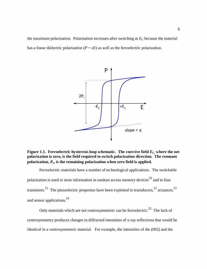
6
the maximum polarization. Polarization increases after switching at EC because the material
has a linear dielectric polarization (P = εE) as well as the ferroelectric polarization.
Figure 1.1. Ferroelectric hysteresis loop schematic. The coercive field EC, where the net
polarization is zero, is the field required to switch polarization direction. The remnant
polarization, Pr, is the remaining polarization when zero field is applied.
Ferroelectric materials have a number of technological applications. The switchable
polarization is used to store information in random access memory devices20
and to bias
transistors.21
The piezoelectric properties have been exploited in transducers,22
actuators,23
and sensor applications.24
Only materials which are not centrosymmetric can be ferroelectric.25
The lack of
centrosymmetry produces changes in diffracted intensities of x-ray reflections that would be
identical in a centrosymmetric material. For example, the intensities of the (002) and the

7
(00-2) reflections are different in Pb(Zr,Ti)O3 thin film capacitors.26
Chapter 3 explores the
effects of polarization reversal in the model ferroelectric material Pb(Zr,Ti)O3.
The polarization of a ferroelectric material is rarely homogeneous – typically, it is
split into regions of uniform polarization called domains which differ in polarization direction
from one another. Ferroelectric domains are regions which have uniform parallel polarization
in the absence of an external electric field. In thin films, ferroelectric domains are the result
of a competition between the energy required to create the depolarization field outside the
material and the energetic cost of creating boundaries between neighboring regions of
different polarization directions.17
The depolarization energy is minimized when the net
polarization is zero, so a material could theoretically reduce this energy by making infinitely
thin domains of opposite polarization direction. Boundaries between polarization domains
also require energy to form, however. The region between domains, called a domain wall,
can be strained by the neighboring domains.27
As a result of the competition between the
depolarization field and the domain wall formation energy, ferroelectric thin films often form
repeating lamellar patterns of domains.28,29
In the x-ray microdiffraction studies of Chapter
2, we observe the structural signatures of these repeating domain patterns.
Ferroelectric materials are also piezoelectric, meaning voltage appears across the
sample when it is mechanically stretched or compressed. In the converse piezoelectric effect,
the lattice expands or contracts when an electric field is applied. Piezoelectric strain is
linearly proportional to the applied electric field. Other phenomena such as electrostriction
can also contribute to the strain, especially at high fields.30
At electric fields less than or
equal to the coercive field, the contribution of electrostriction to strain is small in the

8
materials considered here. In Chapter 4, I determine the piezoelectric strain of BiFeO3 thin
films by measuring the change in lattice constants using x-ray diffraction while an electric
field is applied to a ferroelectric capacitor.
1.4. The perovskite structure
Many multiferroics have a crystal structure similar to the mineral perovskite, in which
a transition metal is the central atom of a cubic or nearly cubic unit cell.31
A large number of
fluoride based materials are magnetic ferroelectrics, but as of yet none have magnetic and
ferroelectric ordering at room temperature.32
Perovskites that are magnetic ferroelectrics in
particular are quite rare because the partially filled d orbitals of the transition metal, which
lead to magnetic ordering, tend to eliminate the cation displacement that causes
ferroelectricity.33
Bismuth-based multiferroics avoid this problem, since the ferroelectricity
arises from the bismuth 6s2 orbitals.
34
Perovskites are a broad class of materials with the general formula ABX3. The
perovskite mineral has a cubic structure with Pm-3m symmetry. The cubic symmetry is
easily distorted, however, because the structure can accommodate ions of many different
elements. As a result materials with tetragonal, orthorhombic, monoclinic, and rhombohedral
symmetry are all found in nature.35,36
The perovskite structure is robust and will expand,
contract, and rotate bond angles in order to accommodate a wide range of cation sizes.
The family of oxides with perovskite-derived structures has a variety of fascinating
properties. Ferroelectricity, large dielectric constants, superconductivity, ferromagnetism,

9
and antiferromagnetism have all been observed in materials with the perovskite structure.9
The versatility of the perovskite structure makes it sensitive to forces which may be too weak
to have significant effects in other structures. Thus, small displacements and distortions from
the ideal structure are an important factor in understanding and manipulating the wide variety
of properties in these materials.
In the ideal perovskite structure, the cubic unit cell has A site atoms in the corners of
the cube, a B site atom in the center, and oxygen atoms centered on the faces of the cube.
This is called the aristotype structure and is shown below in Figure 1.2. Most materials that
are described as having a perovskite structure deviate from the aristotype slightly. The
modified structure is called a hettotype.37
Hettotypes can differ from the aristotype in many
ways; changes to the lattice constants, non-cubic symmetry, and displacements of the A or B
atoms.
Figure 1.2. Perovskite structure ABO3. SrTiO3 and CaRbF3 form this ideal cubic
structure, unlike the mineral perovskite itself (CaTiO3).

10
Two parameters are commonly used to describe how well a material fits in the
perovskite structure. The tolerance factor, t, quantifies the degree to which a particular ABO3
compound fits in this structure:
where rA, rB, and rO are the A site, B site, and oxygen ionic radii, respectively. 38,39
Most
materials that are stable in the perovskite structure have tolerance factors between 0.75 and
1.05. BiFeO3 has a tolerance factor of 0.95. The ratios between A and B ionic radii and rB/rO
are also important in stabilizing the perovskite structure.40
If the B radius is too small, then
the oxygen octahedra are unstable due to oxygen-oxygen ionic repulsion. A site atoms that
have radii less than can be accommodated to some extent by rotations
of oxygen octahedra.37
Compressive strain can also be accommodated by increasing the
rotation angle.
One of the more common modifications to the aristotype is the distortion or rotation of
the oxygen octahedra. Rotations can be caused by A or B site atoms which do not fit, polar
displacements of the A or B site atom, highly directional bonds (for example Pb2+
or Bi3+
on
the A site), and Jahn-Teller distortions of the BO6 octahedra. Tilt systems are described in
terms of rotations of the octahedra about the a, b, and c lattice vectors in the notation used by
Glazer.41
A tilt system with rotations about each axis is written a+ b
+ c
+. The first, second,
and third letter represent a rotation about the a, b, and c axis respectively. Rotations of the
same magnitude about different axes are indicated by using the same letter, such as a+a
+c
+.
The superscript is + when octahedra along the same axis have identical rotations about that

11
axis. A superscript of – indicates an equal but opposite rotation in adjacent octahedra, and a 0
superscript means no rotation about that axis. Glazer described 23 tilt systems found in a
2×2×2 pseudocubic unit cell structure, although Woodward later found there are only 15
systems in which it is possible to keep octahedra of neighboring cells connected.42,43
In this thesis, I study two members of the perovskite family, BiFeO3 and Pb(Zr,Ti)O3.
In both of these materials the B-site atom is not located at the center of the unit cell, which
creates a ferroelectric dipole. Pb(Zr,Ti)O3 is the simpler of the two structures – it is
tetragonal, has an elongated c axis, and the octahedron is distorted and displaced along the c
axis along with the B site atom. BiFeO3 is rhombohedral and has distortions along the
pseudocubic [111] direction. In the next section, I describe the structure and properties of
BiFeO3 in detail.
1.5. Bismuth ferrite
1.5.1. Bulk single crystal BiFeO3
The structure of bulk BiFeO3 is commonly described in three different geometrical
ways. The most accurate description is that BiFeO3 is rhombohedral at room temperature
with the space group R3c. This is equivalent to the hexagonal setting often used by
crystallographers, which has six formula units of BiFeO3 in the hexagonal cell and lattice
constants of ahex
=5.579 Å and chex
= 13.869 Å. However, the most intuitive view of the
structure is found by comparing the pseudocubic setting of BiFeO3 to the perovskite

12
aristotype. The pseudocubic setting contains one formula unit of BiFeO3 and is nearly cubic
(but technically rhombohedral) with apc
= 3.96 Å and αpc
= 89.4°. Bi3+
and Fe3+
sit on the A
and B sites respectively and are both displaced in the same direction along the [111]pc. The
oxygen octahedron is flattened in the same direction, most likely by ionic repulsion from the
Bi lone pair.37
Octahedra are rotated in alternating directions about the [111] axis by 13°,
corresponding to the a-a
-a
- tilt system in the Glazer notation. Two pseudocubic unit cells are
shown below in Figure 1.3.
Figure 1.3. Structure of BiFeO3. Two pseudocubic unit cells are shown. Oxygen
octahedra are shaded blue.
It has been known for several decades that bulk BiFeO3 is ferroelectric, but it was not
until recently that the observed properties12
came close to theoretical predictions of large
remnant polarizations.34
In bulk crystals, BiFeO3 has a remnant polarization up to 100
μC/cm2 parallel to the [111]pc
axis and a coercive field of 12 kV/cm.
12 The remnant

13
polarization is extremely large and is approximately equal to the polarization of common
ferroelectrics such as Pb(Zr,Ti)O3 and BaTiO3 that are currently used for ferroelectric
memories. The coercive field in bulk BiFeO3 is much smaller than in thin films, similar to
other ferroelectric materials.
Despite the large amount of research done on BiFeO3, questions about the type of
antiferromagnetic ordering still remain. The antiferromagnetism of BiFeO3 results in
magnetic reflections in neutron diffraction.44,45
BiFeO3 is a G-type antiferromagnet; spins
on Fe3+
ions are antiparallel to all their nearest neighbors creating planes of parallel spin
along the (111)pc planes. This is the (001)hex plane in the hexagonal setting of the crystal.46
This description proved to be incomplete; neutron scattering evidence for an additional spin
spiral with a period of 62 nm was discovered by Sosnowska et al. in 1982.47
There is still
some debate in the literature of whether the magnetic modulation is cycloidal, elliptic, or even
a spin density wave.48,49
Nevertheless, all evidence points to short range antiparallel coupling
between Fe3+
nearest neighbors.
Coupling between the ferroelectric and antiferromagnetic ordering in BiFeO3 is also
linked to the structure. The ferroelectric polarization direction has been shown to be linked to
the antiferromagnetic wavevector in BiFeO3 thin films. The spin direction and spiral
wavevector can be changed by applying an electric field to switch the ferroelectric
polarization direction.12
The plane of parallel spins then switches so that the plane remains
perpendicular to the polarization.15
The magnetic ordering is strongly influenced by the Fe-

14
O-Fe bond as described in the double exchange model.50
In BiFeO3, density functional
theory calculations suggest that the magnetic interaction is sensitive to the tilt and rotation of
the FeO6 oxygen octahedra.51
One prominent consequence of the multiferroic order of
BiFeO3 would be the magneto-electric effect, in which the net magnetization would be
changed by applying an electric field, or the polarization increased by applying a magnetic
field. 52,53
Although the linear magneto-electric effect is supposedly forbidden by the
symmetry of bulk BiFeO3,54,55
a linear effect in BiFeO3 films has been reported.56,57,58
Problems with bulk single crystals have lead researchers to focus on thin films of
BiFeO3. Although the intrinsic ferroelectric and magnetic properties of bulk single crystals
and epitaxial thin films are similar, the single crystals may prove difficult to use in practical
applications. The biggest problem with single crystal BiFeO3 is in the leakage and fatigue
properties. Lebeugle et al. found that BiFeO3 bulk crystals are susceptible to mechanical
damage caused by repeated polarization reversal.12
The large changes in shape result in the
formation of cracks and defects during the switching process.12
The defects have much
smaller resistivities, so during successive electrical cycling the leakage current heats and
degrades the sample, decreasing the remnant polarization. Lebeugle et al. showed that the
remnant polarization in single crystals can initially reach up to 100 μC/cm2, but show
appreciable degradation after even one switching cycle.12
In comparison, (111)-oriented thin
films grown on SrTiO3 have remnant polarizations up to 95μC/cm2 and can withstand billions
of cycles of polarization switching.59
In other film orientations, the out-of-plane remnant

15
polarization is consistent with a simple geometric projection of the <111> onto the film
normal. The desirable ferroelectric, piezoelectric, and magnetic ordering are almost the same
as the bulk, but the improvement in fatigue properties and decrease in leakage current makes
the thin films more useful than the bulk material.
1.5.2. BiFeO3 thin films
BiFeO3 thin films have lower leakage currents and better resistance to fatigue than
bulk crystals, but the other properties are essentially the same. Early reports did show a
dependence of net magnetization and polarization on film thickness.56
However, later first-
principles calculations using density functional theory predicted very little change of P and M
as a function of strain.60
Epitaxial strain rotates the polarization direction of (001) BiFeO3
films, but does not have a significant effect on the magnitude of the polarization.61
Further
experimental studies of films with thicknesses ranging from 40 nm to 960 nm confirmed that
there was very little change in the magnitude of the polarization, although they found the
coercive field decreases with thickness.62
Even the orientation of the film does not change
the magnitude of the spontaneous polarization. The out-of-plane remnant polarizations for
(111), (101), and (001) BiFeO3 films were measured by Li et al. 63
were found to be P111 ≈
100 μC/cm2, P101≈ 80 μC/cm
2, and P001≈ 55μC/cm
2. These values are consistent with a
spontaneous polarization along [111]pc being projected on the different out of plane
directions, which predicts that P111 ≈ √2 P101≈√3P001. It was thought that epitaxial strain in
thin films of BiFeO3 might induce ferromagnetism, which would be much easier to detect and

16
manipulate in potential applications such as multistate memory.64
The antiferromagnetic
ordering in BiFeO3 has proved to be quite robust despite initial reports of switching
magnetization using an electric field.56
Epitaxial BiFeO3 films can remain coherent above the critical thickness predicted by
Matthews and Blakeslee.65
Matthews and Blakeslee provide an estimate for the maximum
thickness for which thin films can remain strained to the lattice constant of the substrate,
based on the elastic energy stored in the film. We can apply this method to BiFeO3 on
SrTiO3. Assuming that the Poisson ratio of BiFeO3 is 0.3 and misfit dislocations have [110]
type Burgers vectors, the thickest defect free film is expected to be 5-15 nm. Coherent,
metastable films up to 70 nm have been observed experimentally.66
Possible explanations for
the stability of thicker films include misfit dislocations with large nucleation energies,
rotation of the oxygen octahedra to reduce the lattice constant,37
or non-stoichiometry in the
film accommodating strain.67
Partially relaxed films offer an opportunity to learn how strain affects the structural,
ferroelectric, and magnetic properties. Whether induced by thickness or less than optimal
growth conditions, relaxation of epitaxial films affects the magnetic ordering of BiFeO3 films.
The magnetic moment depends on strain. In epitaxial BiFeO3 films on SrTiO3 substrates, the
saturation magnetization decreases as the film relaxes.68
X-ray linear dichroism
measurements of antiferromagnetic and ferroelectric domains in strained 200 nm and relaxed
1 μm-thick BiFeO3 films indicate that the epitaxial strain in the thinner films changes the type

17
of antiferromagnetic ordering.69
The energetic degeneracy for the spin direction within the
(111) plane is lifted when epitaxial strain is applied, and there is an easy axis of
magnetization along the <112> direction.
1.6. Calculating x-ray scattering intensities
The work in this thesis largely consists of using x-ray diffraction to determine
structural parameters including lattice constants, symmetry, and polar displacements. Many
of the experiments compare experimental diffracted x-ray intensities to predicted intensities
in order to determine the validity of different structural models. In this section, I outline the
how the intensities of x-ray reflections can be calculated. Using these equations, I predict
how reflections can be split by the presence of multiple ferroelectric domains (Chapter 2), the
energy dependence of reflections and the effect of polarization direction (Chapter 3),
piezoelectric strain (Chapter 4), and the origin of scattered intensity at ½(hkl) type reflections
(Chapter 5).
Calculating the x-ray scattering intensity starts with the scattering from an atom, then
all the atoms in the crystal‟s unit cell, and then from the unit cells in the entire crystal. When
an x-ray is elastically scattered, we measure the intensity and angle of the scattered beam.
The difference in momentum between the incident (k0) and scattered wavevector (k’) makes a
vector in reciprocal space, q, such that The three-dimensional components
qx qy and qz are related to the x-ray wavelength and angles labeled in Figure 1.4.

18
Figure 1.4. Definition of q, scattering angles and incident and scattered x-ray
wavevectors. α is the incident angle and β is the scattered angle such that α+β = 2θBragg.
γ is the azimuthal angle, and is generally small or zero.
The units of q are 1/Å, such that . This last relation can be
rearranged to form Bragg‟s Law λ=2d sin θ, which gives the relation between the scattered
angle 2θ and the interplanar spacing.
1.6.1. Atomic scattering factors
The scattering from an atom is the sum of scattering from all the electrons bound to it.
The atomic scattering factor is expressed in units of r0, the Thompson scattering length.
Consequently, the atomic scattering factor depends on a number of factors; the element and
bonding of electrons in the scattering atom, the wavevector transfer q, and the photon energy.
All of these are summed up in a single atomic scattering factor, f.

19
where f 0 is the part dependent on q, f ' and f " are the real and imaginary parts of the energy
dependent portion, respectively.
f 0 is approximately the total number of electrons bound to the atom at q = 0, and goes
to zero as q increases. f 0 can be approximated very well by the sum of three exponential
functions with coefficients found by Cromer and Mann.70
These functions fit observed
values of f 0 for |q| less than 2.0 Å
-1. At large |q| or for ionized elements, f
0 is better described
by Waasmeier and Kirfel‟s fitting parameters71
which are discussed in more detail in Section
3.5.
f ' and f " are collectively called the dispersion correction and are assumed to be
independent of q. Dispersion corrections for many elements have been calculated and are
tabulated for x-ray energies between 10 and 30,000 eV.72
The effect of the dispersion
correction on the intensity of Bragg reflections is examined in Section 3.1.2. Typically, it
does not have a large effect unless the x-ray energy is close to an absorption edge of an
element in the material.
1.6.2. Structure factor
The structure factor is the superposition of the scattered wave from each atom in the
unit cell:
∑

20
where q is the wavevector transfer and fn are the atomic scattering factors for each atom n.
is the position for the nth atom and can be written as a linear superposition of the direct
lattice vectors a, b, and c.
The set (u,v,w) are called the fractional indices of the atomic position. The origin (where =
0) is conventionally taken to be one of the corners of the cubic unit cell. For example, the
body-centered atom in a bcc unit cell would have (uvw) = (0.5, 0.5, 0.5).
When q is exactly equal to a reciprocal lattice vector the
structure factor is simplified to
∑
∑
because the reciprocal lattice vector and is orthogonal to and . The
intensity of a reflection is proportional to FF*, where F* is the complex conjugate of the
structure factor. The sign of the imaginary component in F* is reversed for fn and the phase
factor.
X-ray diffraction textbooks including Warren,73
Als-Nielsen,74
Guinier,75
and
Cullity76
differ slightly in their definitions of q and the structure factor Fhkl. The definitions
are different in 1) the sign of q and the sign of the phase factor in Fhkl , and 2) whether a factor
of 2π/λ is included in the definition of q or in the phase factor in Fhkl. No matter which
convention is chosen, the correct phase factor is exp[+2πi (ha*+kb*+lc*)(ua+vb+wc)].

21
1.6.3. Lattice sum
The scattering from the entire crystal is the superposition of the scattering from each
unit cell. To illustrate this more clearly, I first consider the scattering from a one-dimensional
line of M1 unit cells along the a direction. The scattering from the crystal is the superposition
of the scattered waves from each unit cell:
∑
where . The sum can be rewritten as a geometric series
so the sum over m1 becomes
Generalizing to three-dimensional parallelpiped with M2 cells along the b direction and M3
along the c direction,
As M approaches infinity, as in a large single crystal, the lattice sum can be approximated by
a series of delta functions when q equals a reciprocal lattice vector ghkl. The scattered
intensity is proportional to the scattering amplitude times its complex conjugate.
In order to compare calculated scattering amplitudes to real numbers of diffracted
photons, I calculate the structure factor at a reciprocal lattice vector ghkl and compute the
intensity. For a small number of cells, I calculate the structure factor of the atoms of the

22
structure by building a supercell made up of many unit cells separated by lattice vectors
(Chapter 3). For large numbers of unit cells, I typically omit the lattice sum and approximate
I = Fhkl F*hkl, since the lattice sum essentially picks out Fhkl at each reciprocal lattice vector.
This does ignore the problems of mosaic spread in the crystal, dynamical diffraction, and the
effect of the film thickness. However, unless otherwise noted, the films studied here are
sufficiently thick and imperfect so thickness fringes and dynamical effects cannot be
observed. The issue of mosaic spread is addressed by comparing the integrated intensity of
the experimentally observed diffraction peak to the calculated maximum intensity at q = ghkl.
1.7. Experimental methods
X-ray diffraction was used to characterize the structure and electromechanical
properties of BiFeO3 thin films. To completely understand the x-ray scattering, we
investigated the effects of polarization reversal on the diffracted intensity in Pb(Zr,Ti)O3 thin
film capacitors. Hysteresis loops were taken to characterize the BiFeO3 and Pb(Zr,Ti)O3
capacitors and measure the coercive fields. The steady-state structure of BiFeO3 films was
probed with area-averaged diffraction techniques as well as synchrotron microdiffraction.
Next, time resolved x-ray microdiffraction was synchronized with electric fields applied to
BiFeO3 thin film capacitors to measure the piezoelectric response on a local scale. In order to
apply large fields while measuring the piezoelectricity, nanosecond-scale time resolved
diffraction techniques were used.

23
1.7.1. Sample fabrication
The epitaxial BiFeO3 and Pb(Zr,Ti)O3 (001) thin films for this study were grown in the
research group of Prof. Chang-Beom Eom.77
BiFeO3 and Pb(Zr,Ti)O3 layers were deposited
using off-axis sputtering on a SrTiO3 (001) substrate. The Pb(Zr,Ti)O3 and 400 nm BiFeO3
samples had an additional 15 nm thick SrRuO3 layer between the substrate and the
ferroelectric layers. SrRuO3 is a conducting oxide which served as a bottom electrode and
allowed us to create thin film capacitor structures. The BiFeO3 samples were grown on a
substrate that was miscut by 4° towards [010]. The miscut substrate helps promote epitaxial
growth and select the polarization direction of the domains.78
Bulk BiFeO3 samples were grown by Sang-Wook Cheong‟s research group at Rutgers
University using the flux growth method. Single crystals of BiFeO3 were grown using a
Bi2O3/Fe2O3/B2O3 flux by cooling slowly from 870° to 620° C.79
Platelets several
millimeters across with faces parallel to the pseudocubic (001) were obtained. Multiple
ferroelectric domains were observed with x-ray diffraction and with polarized light
microscopy.
1.7.2. Ferroelectric characterization and polarization switching
Electric fields were applied to the sample in the out-of-plane direction by applying a
voltage across platinum top electrodes and the SrRuO3 layer underneath the Pb(Zr,Ti)O3 or
BiFeO3 layers. Circular platinum top electrodes with diameters of 25, 50, 75, 100, and 200
μm were patterned on top of the Pb(Zr,Ti)O3 and BiFeO3 films.

24
Top electrodes were contacted with a high bandwidth 5µm tungsten probe tip
(Cascade Microtech, 107-158). The SrRuO3 bottom electrode was contacted by soldering a
thin platinum wire to an area at the corner of the sample where the film had been removed to
expose the SrRuO3 bottom electrode. This wire was connected to the outer coaxial
connection of the probe tip. This connection is usually grounded in high frequency
experiments. In order to make hysteresis loops, however, we isolated the outer connection
from ground and used it to connect the sample to the resistor we used to measure the
displacement current flowing through the ferroelectric capacitor. Electric fields were applied
to the region underneath the top electrode by applying a voltage across the film thickness
using a function generator (Agilent 33120A).
Ferroelectric switching properties of the films were determined by measuring the
electrical hysteresis loops of capacitor structures. Several periods of a triangle waveform
with a amplitudes of 7 to 10 V were applied to the top electrode. A sample of the poling
pulse train and the switching current is shown in Figure 1.5.

25
Figure 1.5. Voltage and switching current from a 100μm diameter Pb(Zr,Ti)O3
capacitor measured during a poling pulse train resulting in a Pup state.
The current measurement shows that the capacitor is switching and does not have
significant leakage current. The sharp current spikes are the switching current from the
polarization reversing direction to align parallel to the electric field. In leaky devices, the
capacitor develops conduction paths which behave like a resistor in parallel with the
capacitor. At low frequencies, the current through a leaky device at is proportional to the
applied field. This was not observed for the device shown in Figure 1.5.
To obtain a quantitative measurement of the coercive field, we calculated the
polarization versus electric field to get a ferroelectric hysteresis loop. The polarization P is
measured by integrating the displacement current over time, normalizing to the electrode area,
and plotting charge per area as a function of the applied voltage. A hysteresis loop for a 100
μm-diameter Pb(Zr,Ti)O3 capacitor in this sample is shown in Figure 1.6. The coercive fields
were +350 kV/cm and -150 kV/cm. Note that the coercive fields are not the same for positive
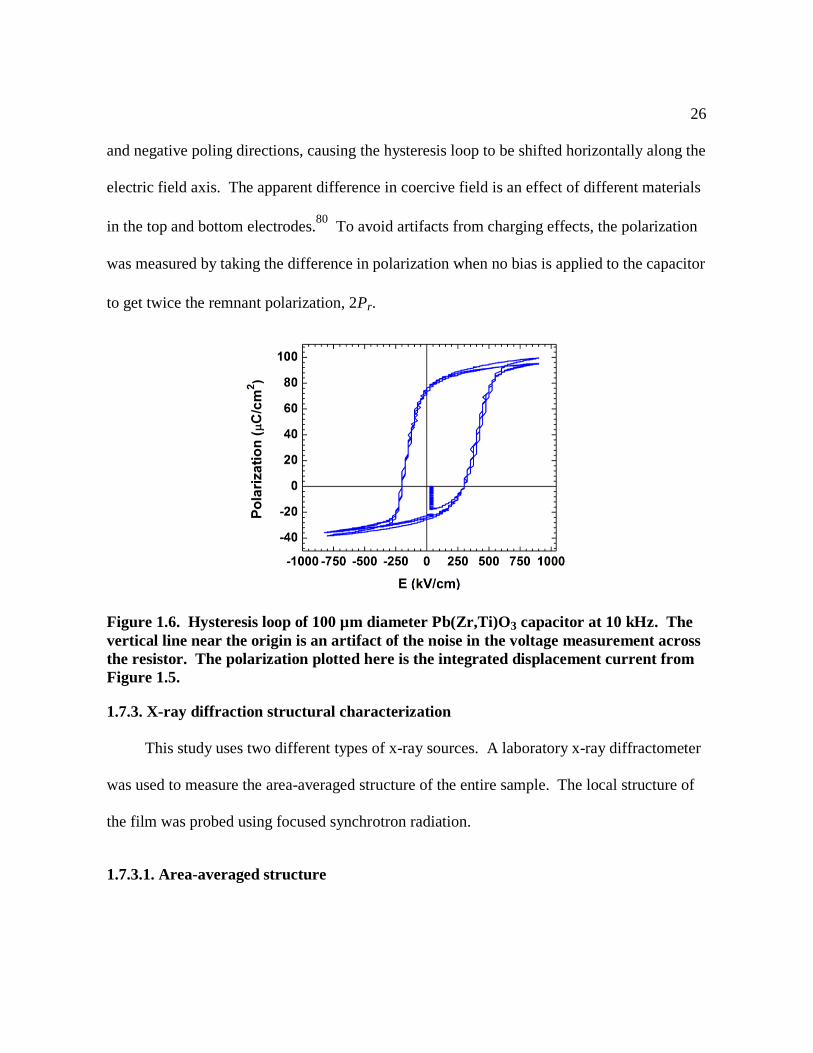
26
and negative poling directions, causing the hysteresis loop to be shifted horizontally along the
electric field axis. The apparent difference in coercive field is an effect of different materials
in the top and bottom electrodes.80
To avoid artifacts from charging effects, the polarization
was measured by taking the difference in polarization when no bias is applied to the capacitor
to get twice the remnant polarization, 2Pr.
Figure 1.6. Hysteresis loop of 100 µm diameter Pb(Zr,Ti)O3 capacitor at 10 kHz. The
vertical line near the origin is an artifact of the noise in the voltage measurement across
the resistor. The polarization plotted here is the integrated displacement current from
Figure 1.5.
1.7.3. X-ray diffraction structural characterization
This study uses two different types of x-ray sources. A laboratory x-ray diffractometer
was used to measure the area-averaged structure of the entire sample. The local structure of
the film was probed using focused synchrotron radiation.
1.7.3.1. Area-averaged structure

27
Laboratory x-ray diffractometers were used to probe the area-averaged structure of
BiFeO3 bulk and thin film samples. The millimeter sized x-ray spots diffract from the entire
sample, giving information about the average structure of the film. Two diffractometers
were used based on a sealed tube source (Panalytical X‟Pert MRD) and on a rotating anode
(Rigaku UltraX 18 Rotaflex). A monochromatic beam with the Cu Kα wavelength, λ =
1.5406, is selected from the spectrum by diffracting from a crystal monochromator. The
sample is mounted on a four-circle diffractometer in a horizontal scattering geometry. Three
degrees of freedom are available to rotate the sample to the Bragg condition (θ, χ, and φ); the
rotation in 2θ brings the detector to the diffracted beam (Figure 1.7). These naming
conventions are used to describe the diffraction geometry through the rest of this thesis.
Figure 1.7. Scattering geometry angle definitions for four circle diffractometers.
The Panalytical diffractometer is designed to measure x-ray diffraction and reflectivity
of thin epitaxial films. Two dimensional slices of reciprocal space were mapped out to
determine the orientation of BiFeO3 films with respect to the substrate, as described in
Chapter 2. The 4-bounce Ge monochromator and large beam (1 mm × 10 mm at the source)
produce the highly collimated beam that is necessary for high resolution measurements of
thin films. Angular resolution in 2θ was set to 0.1° by the detector slits. The film reflections

28
were more than 0.5° wide in 2θ due to the mosaic spread, so higher angular resolution did not
provide any additional information.
The Rigaku rotating anode diffractometer was used for measurements of low-intensity
Bragg reflections. This diffractometer is optimized for low-intensity measurements from
small samples. The rotation of the anode distributes the heat load more evenly so that higher
intensities of x-rays can be produced. This generator was operated in point-focus mode, so
the x-ray spot size at the sample (≈1 mm2) was slightly smaller than for the Panalytical.
Attenuation of the beam was reduced by removing the air inside flight paths between the
source and sample as well as in front of the detector. The Na:I scintillation detector (Saint
Gobain, Bicron 1XPM-040B) is capable of detecting single photons. A lead cap was placed
on the end of the detector to absorb high energy photons. Angular resolution in 2θ was
determined by slits placed in front of the detector.
1.7.3.2. Synchrotron x-ray microdiffraction
Synchrotron light sources provide the intensity required to measure small scattering
signals with a focused x-ray beam. Synchrotron light is coherent and the flux is orders of
magnitude higher than the laboratory x-ray sources.81
These advantages allow for the use of
x-ray focusing optics such as zone plates and mirrors. The x-rays are generated in 100 ps
pulses spaced 153 ns apart, which is useful for time-resolved scattering.82
A schematic of
the entire setup is shown below in Figure 1.8 and each element is discussed below.
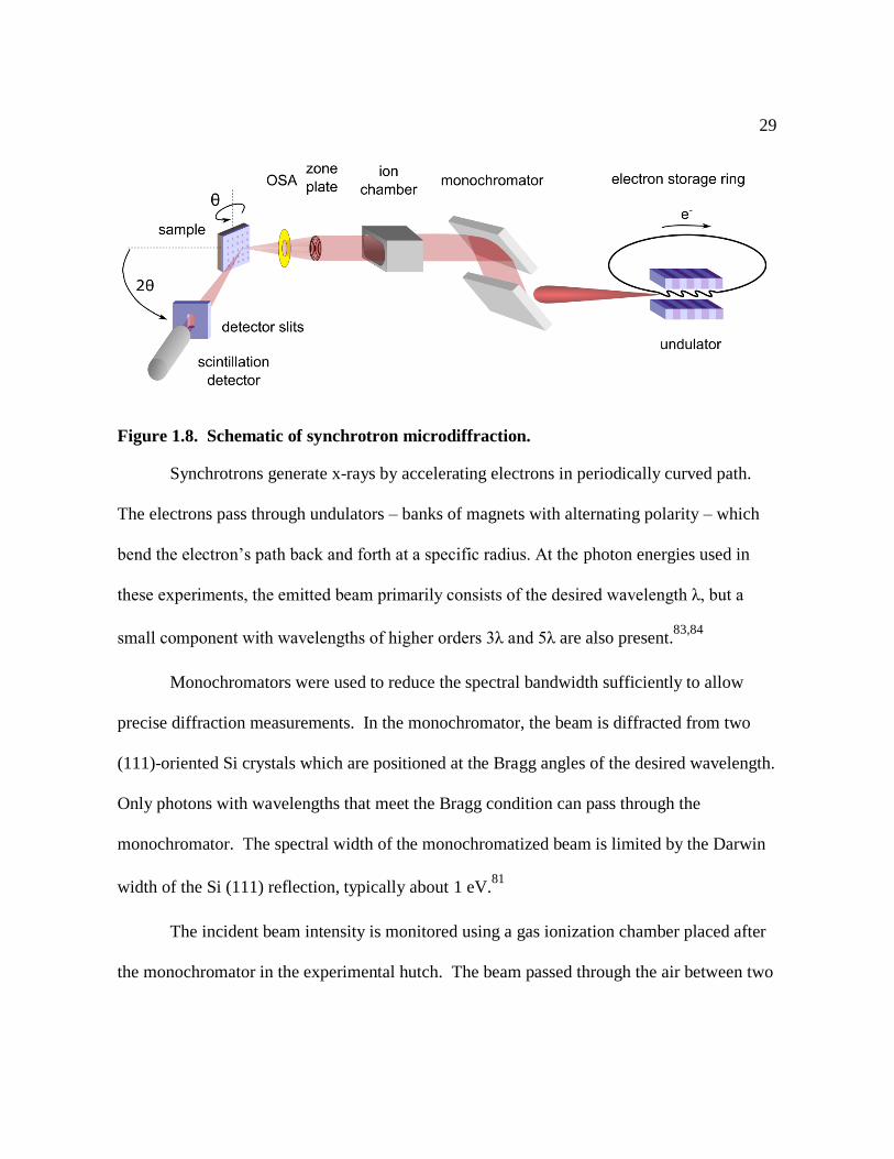
29
Figure 1.8. Schematic of synchrotron microdiffraction.
Synchrotrons generate x-rays by accelerating electrons in periodically curved path.
The electrons pass through undulators – banks of magnets with alternating polarity – which
bend the electron‟s path back and forth at a specific radius. At the photon energies used in
these experiments, the emitted beam primarily consists of the desired wavelength λ, but a
small component with wavelengths of higher orders 3λ and 5λ are also present.83,84
Monochromators were used to reduce the spectral bandwidth sufficiently to allow
precise diffraction measurements. In the monochromator, the beam is diffracted from two
(111)-oriented Si crystals which are positioned at the Bragg angles of the desired wavelength.
Only photons with wavelengths that meet the Bragg condition can pass through the
monochromator. The spectral width of the monochromatized beam is limited by the Darwin
width of the Si (111) reflection, typically about 1 eV.81
The incident beam intensity is monitored using a gas ionization chamber placed after
the monochromator in the experimental hutch. The beam passed through the air between two
30
charged plates. The resulting ionization current is proportional to the beam intensity, but
decreases exponentially with increasing photon energy.85
For several measurements we focused the monochromatic beam using a Fresnel zone
plate. Fresnel zone plates are essentially circular diffraction gratings, with alternating circles
of materials with different indices of refraction.86
The zone plates used in these experiments
consist of patterns of concentric gold rings patterned on Si3N4 membranes. X-rays passing
through the gold Fresnel zones undergo a phase shift. The pattern is designed such that the
phase shifts introduced causes constructive interference at focal spot. The focal distance and
spot size are determined by the zone plate diameter, photon energy, number of zones, and
width of the outermost zone.83
Zone plates are typically used at synchrotron light sources
because coherent x-rays are required and there is a significant loss of intensity (only 10% of
the transmitted beam is focused at the first order focal point.)87
In order to avoid contamination from the unfocused beam, all but the focused beam is
blocked. The unfocused beam is absorbed in two parts – a central beamstop and a pinhole
which acts as an order-sorting aperture. The beamstop is a gold sphere either integrally
mounted on the zone plate or on a separate Si3N4 window. It blocks the direct beam through
the center of the zone plate. The order sorting aperture is placed between the zone plate and
the focal point in order to block the unfocused beam and any focused x-rays from higher
order focal points.
The focused beam is measured by scanning a chromium knife edge across the focal
point and measuring the Cr fluorescence. A knife-edge scan from the 160 μm-diameter zone
plate at Sector 2-ID-D is shown in Figure 1.9.

31
Figure 1.9. Chromium knife edge scan of focused x-ray beam. The sharpest part of the
knife edge was scanned across the focal point of the x-ray beam and the fluorescence
was measured.
The fluorescence signal was fit to a Boltzmann function. The beam size was
estimated as being the width of the Boltzmann function. Typical values for beam size using a
320 μm diameter zone plate at sector 2-ID-D of the Advanced Photon Source are around 400
nm.
Three types of detectors were used to measure the diffracted x-ray beam. Avalanche
photodiodes (APD) have a fast response time. These detectors are useful for high count rates
up to 106 photons per second. An APD was used for nanosecond-scale time-resolved
diffraction experiments. A charge-coupled device (CCD) area detector records the diffracted
intensity from a large portion of reciprocal space at once. It was used to locate the BiFeO3
(103) reflections and measure the splitting between the (103) reflections from multiple

32
domains. A scintillation detector (Saint-Gobain, Bicron) was used for low count rates,
because it was capable of counting single photons and could filter out higher energy photons
to some degree.
1.7.4. Time-resolved microdiffraction
Time-resolved diffraction was used to measure the structural response to electric field
of BiFeO3 films. Two time resolution techniques were used. The slower, millisecond-scale
method employed a multichannel analyzer to obtain the time-resolved signal. The faster,
nanosecond-scale method was a pump-probe type experiment in which only x-ray pulses
synchronized with electrical pulses were counted. The millisecond-scale method had longer
counting times and was able to measure the responses of very weak reflections. The
nanosecond-scale method applied the electric field for very short times, enabling devices to
sustain very high electric fields without undergoing dielectric breakdown.
1.7.4.1. Time-resolved microdiffraction – millisecond time scale
Millisecond-scale time resolved diffraction was used to measure the piezoelectric
response of BiFeO3 and the changes in the intensity of the ½(hkl) reflections. The time
resolved intensity of a reflection was measured while an electric field was applied to a
capacitor on the sample. Thus, the structural response to an electric field was determined.
There were three challenges here – time resolved diffraction, focusing the beam inside a
capacitor, and synchronizing the electric field with the time resolved measurements.
The microdiffraction techniques discussed above were used to focus the x-ray beam to
a small spot on the sample. Changes in the diffracted intensity and/or the fluorescence from
33
the platinum electrodes were used to determine the position of the x-ray beam on the sample
surface. By mapping areas on the surface, it was possible to image the electrode pattern and
place a focused beam on the same top electrode as the electrical probe tip. This ensured that
the diffraction volume was entirely within the capacitor and only regions subjected to electric
field were probed.
A multichannel analyzer (MCA) was used to record the diffracted intensity as a
function of time. The MCA measured the counts from the detector over a 2 second period in
2 ms steps. Any counts which were detected during each 2 ms bin were summed together.
The MCA output the time resolved intensity in the form of total counts in each of the 2000
bins. Thus, the time resolution was determined by the MCA counting time per bin. This
counting time could be set as low as 8μs, but short counting times proved to be impractical
for low-intensity reflections.
We applied an electric field and simultaneously measured the time-dependent
intensity. A function generator (Agilent 33120A) was configured to produce linearly varying
voltages similar to the triangle pulses in Figure 1.5. The output of the function generator was
connected to the electrical probe tip contacting the capacitor top electrode. The bottom
electrode was grounded. The function generator was triggered at the same time as the MCA,
so the intensity was measured while a series of triangle pulses was applied to the capacitor.
By matching the time dependence of the voltage with that of the intensity, we obtained the
diffracted intensity as a function of electric field. We summed over thousands of repetitions
in order to obtain the time-dependent intensity at each point in reciprocal space.

34
1.7.4.2. Time resolved microdiffraction – nanosecond time scale
Nanosecond-scale time resolved diffraction was used to measure the piezoelectric
strain in BiFeO3 at electric fields above the DC dielectric breakdown limit. Previous studies
have found that ferroelectrics subjected to large electric fields do not undergo dielectric
breakdown if the pulses have short durations (tens of nanoseconds).88
Short pulse durations
also reduce the amount of resistive heating from leakage current which helps increase device
longevity. By measuring the diffracted intensity from single bunches synchronized with short
pulses, we were able to measure the piezoelectric strain at large electric fields.
Short voltage pulses were applied to capacitors at the same time as x-ray bunches
diffracted from the sample. The electric field was applied to capacitors by a pulse generator
(Picosecond Pulse Labs, 2600C). Top electrodes were contacted by the electrical probe tip.
A thin platinum wire connected the SrRuO3 bottom electrode to the shielding of the probe tip.
Square voltage pulses were applied to the top electrode by a pulse generator with adjustable
amplitudes and durations. Typical pulse durations were 15 to 30 ns, with rise times below
300 ps. The pulse generator was triggered by a signal from the timing circuit described below.
The diffracted signal from one x-ray bunch was synchronized with the electric field.
An APD detector was chosen to detect the diffracted x-rays because its response is short than
the time between x-ray bunches. We selected the APD signal from a single bunch which
coincided with the applied voltage pulse. The detector gating and pulse generator triggering
electronics required to do this are described in Grigoriev et al.89
The time between the

35
selected x-ray bunch and voltage pulses was adjusted by delaying the trigger signals for the
pulse generator and APD gate with delay generators (Stanford Research Systems, DG535).
The experiment is shown schematically in Figure 1.10.
Figure 1.10. Schematic diagram of time resolved microdiffraction. The focused x-ray
beam probes the region of BiFeO3 underneath a top electrode contacted by the probe tip
while an electric field is applied.
The synchronization was tested by measuring the time-dependent intensity at the peak
of a Bragg reflection. When an electric field was applied, the film was piezoelectrically
strained which modified the lattice constants. A decrease in diffracted intensity at the peak of
a reflection indicated that the voltage pulse was applied at the same time as the selected x-ray
bunch. The only x-rays that were counted had diffracted from the sample when the electric
field was being applied.
Many voltage pulses/x-ray bunches pairs had to be measured at each point in
reciprocal space. The APD could only measure one count per pulse, so a typical θ-2θ scan

36
would require thousands of pulses at each point in order to distinguish the Bragg reflection
from the background. Typically thousands of pulses were applied at each point in a scan in
order to improve counting statistics.
1.8. Summary
As BiFeO3 films relax, the epitaxial strain is relieved and the film approaches the bulk
structure. The magnetic properties are strongly influenced by the Fe-O-Fe bond angle, which
changes as a function of rotation of the oxygen octahedra. The octahedral rotation angle is
affected by the epitaxial strain and piezoelectric expansion. In order to understand the
coupling between electrical and magnetic order parameters in BiFeO3, we first have to
understand the relationship between substrate, structure, and electric field. In the following
chapters, I describe how the x-ray diffraction techniques outlined above were used to
determine that the strain state, piezoelectric response, and cation displacements vary on the
micron scale in BiFeO3 thin films.

37
1.9. Chapter 1 references
1 H. Schmid, “Multiferroic Magnetoelectrics,” Ferroelectrics 162, 317 (1994).
2 H. Schmid, “Some symmetry aspects of ferroics and single phase multiferroics,” J. Phys.:
Condens. Matter 20, 434201 (2008).
3 N. A. Spaldin and M. Fiebig, “The Renaissance of Magnetoelectric Multiferroics,” Science
309, 391 (2005).
4 B. G. Park, J. Wunderlich, X. Marti, V. Holy, Y. Kurosaki, M. Yamada, H. Yamamoto, A.
Nishide, J. Hayakawa, H. Takahashi, A. B. Shick, and T. Jungwirth, “A spin-valve-like
magnetoresistance of an antiferromagnet-based tunnel junction,” Nature Mater. 10, 347
(2011).
5 M. Bibes and A. Barthélémy, “Multiferroics: Towards a magnetoelectric memory,” Nature
Materials 7, 425 (2008).
6 H. Bea, M. Bibes, M. Sirena, G. Herranz, K. Bouzehouane, E. Jacquet, S. Fusil, P. Paruch,
M. Dawber, J. P. Contour, and A. Barthelemy, “Combining half-metals and multiferroics into
epitaxial heterostructures for spintronics,” Appl. Phys. Lett. 88, 062502 (2006).
7 Y. -H. Chu, M. P. Cruz, C. -H. Yang, L. W. Martin, P .-L. Yang, J. -X. Zhang, K. Lee, P. Yu,
L. -Q. Chen, and R. Ramesh, “Domain control in multiferroic BiFeO3 through substrate
vicinality,” Adv. Mater. 19, 2662 (2007).
8 H. W. Jang, D. Ortiz, S. H. Baek, C. M. Folkman, R. R. Das, P. Shafer, Y. Chen, C. T.
Nelson, X. Pan, R. Ramesh, and C. B. Eom, “Domain engineering for enhanced ferroelectric
properties of epitaxial (001) BiFeO3 thin films,” Adv. Mater. 21, 817 (2009).
9 Y. Tokura (ed.), Colossal Magnetorestive Oxides, (Gordon and Breach Science Publishers,
Amsterdam, Netherlands, 2000).
10 M. Bibes and A. Barthelemy, “Multiferroics: Towards a magnetoelectric memory,” Nature
Mater. 7, 425 (2008).
11 H. Bea, M. Gajek, M. Bibes, and A. Barthelemy, “Spintronics with multiferroics,” J. Phys.:
Cond. Mat. 20, 434231 (2008).
12 D. Lebeugle, D. Colson, A. Forget, M. Viret, A. M. Battaille, and A. Gukasov, “Electric-
Field-Induced Spin Flop in BiFeO3 Single Crystals at Room Temperature”, Phys. Rev. Lett.
100, 227608 (2008).

38
13
P. Fischer, M. Polomska, I. Sosnowska, and M. Szymanski, “Temperature-dependence of
the crystal and magnetic structures of BiFeO3,” J. Phys. C 13, 1931 (1980).
14 J. R. Teague, R. Gerson, W. J. James, “Dielectric hysteresis in single crystal BiFeO3” Solid
State Commun. 8,1073 (1970).
15 T. Zhao, A. Scholl, F. Zavaliche, K. Lee, M. Barry, A. Doran, M. P. Cruz, Y. H. Chu, C.
Ederer, N. A. Spaldin, R. R. Das, D. M. Kim, S. H. Baek, C. B. Eom, and R. Ramesh,
“Electrical control of antiferromagnetic domains in multiferroic BiFeO3 films at room
temperature,” Nature Mater. 5, 823 (2006).
16 J. H. Lee, K. M. Rabe, “Coupled magnetic-ferroelectric metal-insulator transitions in
epitaxially-strained SrCoO3 from first principles,” arXiv:1104.2856v1
17 M. E. Lines and A. M. Glass, Principles and Applications of Ferroelectric and Related
Materials, (Oxford University Press, New York, 2001).
18 M. Dawber, K. M. Rabe, and J. F. Scott, “Physics of Thin Film Ferroelectric Oxides”, Rev.
Mod. Phys. 77, 1083 (2005).
19 J. F. Scott, “Ferroelectrics go bananas,” J. Phys. Cond. Matter 20, 021001 (2000).
20 G. R. Fox, R. Bailey, W. B. Kraus, F. Chu, S. Sun, and T. Davenport, “The current status
of FeRAM,” in Ferroelectric Random Access Memories: Fundamentals and Applications
(Springer-Verlag, 2004).
21 H. Kohlstedt, Y. Mustafa, A. Gerber, A. Petraru, M. Fitsilis, R. Meyer, U. Bottger, and R.
Waser, “Current status and challenges of ferroelectric memory devices”, Microelectronic
Engineering 80, 296 (2005).
22 A. A. Vives, Piezoelectric Transducers and Applications, (Springer, 2008).
23 A. York, “Experimental characterization and modeling of electro-mechanically coupled
ferroelectric actuators.” PhD Thesis (2008).
24 R. L. Smith, The Electrical Engineering Handbook, edited by R. C. Dorf, (CRC Press,
1997). Chapter 56.
25 J. F. Nye, Physical Properties of Crystals, (Oxford University Press, 1985).
26 D.-H. Do, P. G. Evans, E. D. Isaacs, D. M. Kim, C.-B. Eom and E. M. Dufresne, "Structural
visualization of polarization fatigue in epitaxial ferroelectric oxide devices," Nature Mater. 3,
365 (2004).

39
27
M. J. Hytch, E. Snoeck, R. Kilaas, “Quantitative measurement of displacement and strain
fields from HREM micrographs,” Ultramicroscopy 74, 131 (1998).
28 G. B. Stevenson and K. R. Elder, “Theory for equilibrium 180 degrees stripe domains in
PbTiO3 films,” J. Appl. Phys. 100, 051601 (2006).
29 S. K. Streiffer and C. B. Parker, “Domain patterns in epitaxial rhombohedral ferroelectric
films. I. Geometry and experiments” J. Appl. Phys. 83, 2744 (1998).
30 V. Sundar and R. E. Newnham, The Electrical Engineering Handbook, edited by R. C.
Dorf, (CRC Press, 1997). Chapter 50.
31 S. W. Cheong and M. Mostovoy, “Multiferroics: a magnetic twist for ferroelectricity,”
Nature Mater. 6, 13 (2007).
32 J F Scott and R Blinc, “Multiferroic magnetoelectric fluorides: Why are there so many
magnetic ferroelectrics?” J. Phys.: Condens. Matter 23, 113202 (2011).
33 N. A. Hill, “Why are there so few magnetic ferroelectrics”, J. Phys. Chem. B 104, 6694
(2000).
34 J. B. Neaton, C. Ederer, U. V. Waghmare, N. A. Spaldin, and K. M. Rabe “First-principles
study of spontaneous polarization in multiferroic BiFeO3,” Phys. Rev. B 71, 014113 (2005).
35 C. Li, K. Chi, K. Soh, and P. Wu, “Formability of ABO3 perovskites,” Journal of Alloys and
Compounds 372, 40 (2004).
36
L. Liu, “Silicate Perovskites: A Review,” Surveys in Geophysics 10, 63 (1989).
37 H. D. Megaw and C. Darlington, “Geometrical and Structural Relations in the
Rhombohedral Perovskites”, Acta Cryst. A 31, 161 (1975).
38 M. Johnsson and P. Lemmens, “Crystallography and Chemistry of Perovskites” in
Handbook of Magnetism and Advanced Magnetic Media, (ed. H. Kronmüller), (John Wiley &
Sons, New York, 2006).
39 V.M. Goldschmidt, Skrifer Norske Videnskaps-Akad. Oslo, I.Mat.-Nat. Kl. 8 (1926).
40 C. Li, K. C. K. Soh, P. Wu, “Formability of ABO3 Perovskites,” Journal of Alloys and
Compounds 372, 40 (2004).
40
41
A. M. Glazer, “The Classification of Tilted Octahedra in Perovskites,” Acta Cryst. B 28,
3384 (1972).
42 P.M. Woodward, “Octahedral Tilting in Perovskites. I. Geometrical Considerations” Acta
Cryst. B 53, 32 (1997).
43 P.M. Woodward, “Octahedral Tilting in Perovskites 2. Structure Stabilizing Forces,” Acta
Cryst. B 53, 44 (1997).
44 C. Michel, J. M. Moreau, G. D. Achenbach, R. Gerson, R. and J. W. James, Solid State
Commun. “Atomic Structure of BiFeO3,” 7, 701 (1969).
45 S. V. Kiselev, R. P. Ozerov and S. G. Zhdanov, Sou. Phys.-Dokl. 7, 742 (1963).
46 C. Blaauw and F. Vanderwoude, “Magnetic and Structural Properties of BiFeO3”, Journal
of Physics C – Solid State Physics 6, 1422 (1973).
47 I. Sosnowska, T. Peterlin-Neumaier and E. Steichele, “Spiral magnetic ordering in bismuth
ferrite,” J. Phys. C: Solid State Phys. 15, 4835 (1982).
48 S. Lee, T. Choi, W. Ratcliff, R. Erwin, S. W. Cheong, and V. Kiryukhin, “Single
ferroelectric and chiral magnetic domain of single-crystalline BiFeO3 in an electric field,”
Phys. Rev. B 78, 100101 (2008).
49 R. Przenioslo, M. Regulski, I. Sosnowska, “Modulation in multiferroic BiFeO3: Cycloidal,
elliptical or SDW?,” J. Phys. Soc. Japan 75, 084718 (2006).
50 J. B. Goodenough, “Theory of the role of covalence in the perovskite-type manganites
[La,M(II)]MnO3,” Phys. Rev. 100, 564 (1955).
51 C. E. Ederer and N. A. Spaldin, “Weak ferromagnetism and magnetoelectric coupling in
bismuth ferrite,” Phys. Rev. B 71, 060401 (2005).
52 S. Picozzi and C. Ederer, “First principles studies of multiferroic materials,” J. Phys.
Condens. Matter 21, 303201 (2009) 53
H. Schmid, “On a magnetoelectric classification of materials,” Int. J. Magn. 4, 337 (1973).
54 A. Reyes, C. de la Vega, Ma.E. Fuentes and L. Fuentes, “BiFeO3: Synchrotron radiation
structure refinement and magnetoelectric geometry,” Journal of the European Ceramic Society
27, 3709 (2007).

41
55
C. Tabares-Muñoz, J. –P. Rivera, A. Bezinge, A. Monnier, and H. Schmid, “Measurement
of the Quadratic Magnetoelectric Effect on Single Crystalline BiFeO3 ” Jpn. J. Appl. Phys. 24,
1051 (1985).
56 J. Wang, J. B. Neaton, H. Zheng, V. Nagarajan, S. B. Ogale, B. Liu, D. Viehland, V.
Vaithyanathan, D. G. Schlom, U. V. Waghmare, N. A. Spaldin, K. M. Rabe, M. Wuttig, and
R. Ramesh, “Epitaxial BiFeO3 multiferroic thin film heterostructures”, Science 299, 1719
(2003).
57 Yu.F. Popov, A.M. Kadomtseva and S.S. Krotov et al., “Features of the magnetoelectric
properties of BiFeO3 in high magnetic fields,” Low Temp. Phys. 27, 478 (2001).
58 A.K. Zvezdin, A.M. Kadomtseva and S.S. Krotov, “Magnetoelectric interaction and
magnetic field control of electric polarization in multiferroics,” J. Magn. Magn. Mater. 300,
224 (2006).
59 H. Bea, M. Bibes, X. H. Zhu, S. Fusil, K. Bouzehouane, S. Petit, J. Kreisel, and A.
Barthelemy, “Crystallographic, magnetic, and ferroelectric structures of bulklike BiFeO3 thin
films,” Appl. Phys. Lett. 93, 072901 (2008).
60 C. Ederer and N. A. Spaldin, “Influence of strain and oxygen vacancies on the
magnetoelectric properties of multiferroic bismuth ferrite”, Phys. Rev. B 71, 224103 (2005).
61 H. W. Jang, S. H. Baek, D. Ortiz, C. M. Folkman, R. R. Das, Y. H. Chu, P. Shafer, J. X.
Zhang, S. Choudhury, V. Vaithyanathan, Y. B. Chen, D. A. Felker, M. D. Biegalski, M. S.
Rzchowski, X. Q. Pan, D. G. Schlom, L. Q. Chen, R. Ramesh, and C. B. Eom, “Strain-
Induced Polarization Rotation in Epitaxial (001) BiFeO3 Thin Films,” Phys. Rev. Lett. 101,
107602 (2008).
62 D. H. Kim, H.N. Lee, M. D. Biegalski, and H. M. Christen, “Effect of epitaxial strain on
ferroelectric polarization in multiferroic BiFeO3 films”, Adv. Phys. Lett. 92, 012911 (2008).
63 J. Li, J. Wang, M. Wuttig, R. Ramesh, N. Wang, B. Ruette, A. P. Pyatoakov, A. K. Zvezdin,
and D. Viehland, “Dramatically enhanced polarization in (001), (101), and (111) BiFeO3 thin
films due to epitiaxial-induced transitions”, Appl. Phys. Lett. 84, 5261 (2004).
64 J. F. Scott, “Multiferroic Memories,” Nature Mater. 6, 256 (2007).
65 J. W. Matthews and A. E. Blakeslee, ”Defects in Epitaxial Multilayers,” J. Cryst. Growth
27, 118 (1974).

42
66
H. Béa, M. Bibes, M. Sirena, G. Herranz, K. Bouzehouane, E. Jacquet, S. Fusil., P. Paruch,
M. Dawber, J.-P. Contour, and A. Barthélémy, “Combining half-metals and multiferroics into
epitaxial heterostructures for spintronics,” Appl. Phys. Lett. 88, 062502 (2006).
67 J. Simon, Th. Walther, W. Mader, et al., “Diffusion and segregation effects in doped
manganite/titanate heterostructures,” Appl. Phys. Lett. 84, 3882 (2004).
68 M.S. Kartavtseva, O. Yu. Gorbenko, A.R. Kaul, T.V. Murzina, “The influence of epitaxial
strain on magnetic and electrical properties of BiFeO3 thin films”, Thin Solid Films 518, 4750
(2010).
69 M. B. Holcomb, L. W. Martin, A. Scholl, Q. He, P. Yu, C.-H. Yang, S. Y. Yang, P.-A.
Glans, M. Valvidares,M. Huijben, J. B. Kortright, J. Guo, Y.-H. Chu, and R. Ramesh,
“Probing the evolution of antiferromagnetism in multiferroics”, Phys. Rev. B 81, 134406
(2010).
70 D. T. Cromer and B. Mann, “X-Ray Scattering Factors Computed From Numerical
Hartree-Fock Wave Functions,” Acta Cryst. A 24, 321, (1968).
71 D. Waasmaeir and A. Kirfel, “New Analytical Scattering Factor Functions for Free Atoms
and Ions for Free Atoms and Ions,” Acta. Crys. A 51, 416 (1995).
72 B.L. Henke, E.M. Gullikson, and J.C. Davis, “`X-ray Interactions: Photoabsorption,
Scattering, Transmission, and Reflection at E=50-30,000 eV, Z=1-92,'' Atomic Data and
Nuclear Data Tables 54, 181 (1993).
73 B.E. Warren, X-ray Diffraction, (Dover Publications, New York, 1990).
74 J. Als-Nielsen and D. McMorrow, Elements of Modern X-ray Physics, (John Wiley & Sons,
West Sussex, England, 2001).
75 A. Guinier, X-ray Diffraction In Crystals, Imperfect Crystals, and Amorphous Bodies,
(W.H. Freeman and Co., 1963).
76 B. D. Cullity and S. R. Stock, Elements of X-ray Diffraction (3
rd edition), (Prentice Hall,
2001).
77 R. R. Das, D. M. Kim, S. H. Baek,, C. B. Eom, F. Zavaliche, S. Y. Yang, R. Ramesh, Y. B.
Chen, X. Q. Pan, X. Ke, M. S. Rzchowski, and S. K. Streiffer, “Synthesis and ferroelectric
properties of epitaxial BiFeO3 thin films grown by sputtering,” Appl. Phys. Lett. 88, 242904
(2008).
43
78
Y. -H. Chu, M. P. Cruz, C. -H. Yang, L. W. Martin, P .-L. Yang, J. -X. Zhang, K. Lee, P.
Yu, L. -Q. Chen, and R. Ramesh, “Domain control in multiferroic BiFeO3 through substrate
viscinality,” Adv. Mater. 19, 2662 (2007).
79 T. Choi, S. Lee, Y. J. Choi, V. Kirukhin, S.-W. Cheong, “Switchable Ferroelectric Diode
and Photovoltaic Effect in BiFeO3,” Science 324, 63 (2009).
80 K. M. Rabe, C. H. Ahn, and J. M. Triscone, Physics of Ferroelectrics, (Springer-Verlag,
Berlin, 2007). Chapter 1.
81 J. Als-Nielsen and D. McMorrow, Elements of Modern X-ray Physics, (John Wiley & Sons,
West Sussex, England, 2001).
82 Advanced Photon Source operating parameters,
http://www.aps.anl.gov/Facility/Storage_Ring_Parameters/node5.html, downloaded
7/22/2011.
83 D. Attwood, Soft X-rays and Extreme Ultraviolet Radiation: Principles and Applications
(Cambridge University Press, 1999).
84 K. J. Kim, X-ray Data Booklet, (Lawrence Berkeley National Lab, 2009), Section 2.1B
85 A. C. Thompson, X-ray Data Booklet, (Lawrence Berkeley National Lab, 2009), Section 4.5
86 K. Miyamoto, “The Phase Fresnel Lens,” J. Opt. Soc. Am. 51, 17 (1961).
87 A. I. Erko, V. V. Aristov, and B. Vidal, Diffraction X-ray Optics, (Institute of Physics
Publishing, 1996). Chapter 2.
88 A. Grigoriev, R. Sichel, H.-N. Lee, E. C. Landahl, B. Adams, E. M. Dufresne, and P. G.
Evans, "Nonlinear Piezoelectricity in Epitaxial Ferroelectrics at High Electric Fields," Phys.
Rev. Lett. 100, 027604 (2008).
89 A. Grigoriev, D.-H. Do, P. G. Evans, B. W. Adams, E. Landahl, and E. M. Dufresne,
"Synchronizing fast electrically driven phenomena with synchrotron x-ray probes," Rev. Sci.
Instrum. 78, 023105 (2007).
44
Chapter 2. Anisotropic Relaxation of Epitaxial (001) BiFeO3 Thin
Films
2.1. Introduction
The piezoelectricity, ferroelectric domain structure, and multiferroic properties of thin
film BiFeO3 are influenced by aspects of the structure at length scales ranging from single-
unit cell to the mesoscopic scale of mosaic blocks. In (001) thin films, BiFeO3 is distorted by
epitaxial strain and signatures of monoclinic,1,2
tetragonal,3,4
or even coexisting
rhombohedral and tetragonal5 overall symmetries have been reported. For coherent thin films
without misfit dislocations, the consensus is that BiFeO3 is strained into a monoclinic state
for moderate compressive strains up to 3-4%.2,6,7,8
At compressive strains above 4.5%,
BiFeO3 exhibits coexisting phases.5 The structure of partially relaxed films is more
complicated problem which has not yet been completely solved.
An additional difficulty in determining the structure is that epitaxial thin films of
BiFeO3 are often deposited on miscut substrates to assist the epitaxial growth process. A
substrate which is miscut by several degrees promotes epitaxial growth by providing a high
density of step edges at the surface. Step edges are lower-energy nucleation sites and assist in
stabilizing the step-flow growth mode.9,10
Furthermore, the magnitude and crystallographic
direction of the substrate miscut influence the polarization direction in the BiFeO3 layers.11
The large density of steps and kinks on the surface also appears to help retention of the
45
volatile Bi species in the film and maintain the desired stoichiometry.12
However, the vicinal
surface can affect the film symmetry in unexpected ways. Miscut substrates stretch or
compress the film along the plane defined by the average surface of the substrate. When the
atomic planes are not parallel to the surface, different stresses are projected onto the in-plane
crystallographic directions of the film. This anisotropic stress changes the structure.
The ferroelectric domain structure present in the film influences the electrical,
ferroelectric, and multiferroic properties. In BiFeO3 the conductivity of a (001) film depends
on the domain pattern and type of domain wall.13
The dynamics of ferroelectric switching is
affected by defects at the junctions between different types of domain walls.14
The domain
structure also changes the exchange bias with neighboring ferromagnetic layers and affects
the piezoelectric properties.15,16
Understanding how the substrate affects the domain pattern
is an important step towards tailoring the properties of BiFeO3 films.
We have used x-ray diffraction to study the effects of the miscut of the substrate on
the ferroelectric domain structure, the relaxation of the thin film via dislocations and other
defects, and on the anisotropic stress imposed on the film. Diffraction patterns acquired with
a large x-ray spot provide information that is averaged over the entire area of the film. These
large-spot-size diffraction patterns demonstrate that the crystallographic axes of the film with
respect to the substrate that cause anisotropy in the atomic-scale processes that lead to
relaxation. Synchrotron x-ray microdiffraction with a focused x-ray beam was used to probe
the structure on the scale of individual mosaic blocks, revealing that there are multiple
ferroelectric domains within each mosaic block. The diffraction patterns of off-specular
reflections from individual mosaic blocks are consistent with relaxed stripe domains,
46
following a ferroelectric domain structure previously observed in other ferroelectric thin
films.
2.2. Experimental methods
The samples used in this study were (001) BiFeO3 epitaxial thin films deposited using
off-axis radio frequency sputtering.11,12
The sample consisted of a 400 nm BiFeO3 film on a
15 nm SrRuO3 (SrRuO3) layer deposited on a miscut (001) SrTiO3 substrate. The substrate
was miscut so the sample surface normal was rotated towards the [010] direction by
approximately 3° from the [001].
The area-averaged structure of the BiFeO3 layers was analyzed using x-ray diffraction
(X‟Pert Panalytical MRD). This diffractometer uses a beam with a cross-section extending 1
mm in the horizontal diffraction and 10 mm in height, larger than the approximately 5 mm
lateral size of the sample. This instrument used the characteristic radiation from a copper
target with an x-ray energy of 8.05 keV. The diffracted beam thus provides information about
the structure of the entire BiFeO3 layer.
Structure on the local scale can be very different from the macroscopic average. By
focusing an x-ray beam, diffraction can be used to probe the micron-scale structure of the
layer. Synchrotron x-ray microdiffraction studies were conducted at station 2-ID-D of the
Advanced Photon Source. An 11.5 keV x-ray beam was focused to a 275 nm spot by a
Fresnel zone plate as described in Section 1.7.4. The sample was mounted on the
diffractometer so that the [010] direction of the SrTiO3 substrate was perpendicular to the

47
scattering plane. Diffracted photons were collected by either an avalanche photodiode
detector (APD) or a charge-coupled device (CCD) area detector.
Reciprocal space maps were acquired by rotating the sample to vary the incident
angle of the x-ray beam, while the CCD detector was held at a fixed position. The angular
position of each pixel in the CCD was calibrated by measuring the position of the direct beam
on the CCD at several positions of the detector arm. The detector arm was then moved to 2θ
of the Bragg condition and the incident angle was scanned in discrete steps. A CCD image
was captured at each incident angle. The reciprocal space vector of each pixel in the series of
images was calculated from three angles as in Section 1.5; 2θ and χ were determined by the
pixel position, θ by the incident angle. Two-dimensional maps were created by summing the
intensity of all pixels at the same 2θ and calculating only qx and qz.
2.3. Film rotation caused by substrate miscut
Miscut substrates apply anisotropic stresses to epitaxial films. The effects of these
stresses on the area-averaged BiFeO3 lattice constants, relaxation processes, and the
orientation of the atomic planes were studied in a laboratory x-ray diffraction experiment.
The (002) reflection from the BiFeO3 thin film was used to determine the c-axis lattice
constants and orientation of the BiFeO3. A similar set of planes indexed as (220) were used
to analyze the SrRuO3 layer. By comparing the orientations of the BiFeO3 and SrRuO3 to
that of the substrate, we observe that both films are rotated. These rotations were in opposite
directions and were caused by two different relaxation mechanisms.

48
2.3.1. Measurement of film rotation: direction and magnitude
Geometric relationships between the atomic planes of a film and substrate can be
inferred from the crystallographic orientations. In pseudomorphic (001) oriented films, a and
b are identical to those of the substrate. This requires the (00l) reciprocal lattice vectors of
film and substrate to be parallel: g00l = l (a×b) / V. 17
Differences in the unit cell volumes
Vfilm and Vsubstrate can change the magnitude but not the direction of g00l. Since reciprocal
lattice vectors are perpendicular to the planes they represent, the (00l) planes of a
pseudomorphic (001) film and substrate are expected to be parallel.
Our initial x-ray diffraction experiments showed that the (00l) atomic planes in the
BiFeO3 thin film were not parallel to the planes of the SrTiO3 substrate. In order to
investigate further, x-ray diffraction patterns of the (002) reflections were taken to determine
the orientation of the BiFeO3. Our first indication that the BiFeO3 was rotated with respect to
the substrate was that the maxima for the BiFeO3 pseudocubic (002) reflection and the
SrTiO3 (002) reflection could not be obtained in a single θ-2θ scan. Instead, these reflections
were observed with a small difference between the incident and Bragg angles. We defined
the offset angle to be the difference between the incident angle θ, measured with respect to
the sample surface, and the Bragg angle 2θ, such that offset = θ - ½(2θ). Our observation that
the substrate and film could not be observed in the same -2 scan indicated that the SrTiO3
and BiFeO3 had different offset angles and that their (002) planes were thus not parallel.
The key in defining the orientation of the BiFeO3 thin film was to identify an
unambiguous reference for the angular positions of x-ray reflections. We determined the

49
orientation of SrTiO3 (002) planes and characterized the miscut to provide this orientation
reference. We measured the incident angle of the SrTiO3 (002) maximum from θ scans as a
function of azimuthal angle to determine the direction and magnitude of the substrate
miscut, as shown in Figure 2.1. We called the azimuthal angle to be consistent with the
names of the angles on x-ray diffractometers. The sample was placed so that two edges of the
square substrate were horizontal when = 0° because the edges are nearly parallel to the
SrTiO3 <100> directions. The offset at the SrTiO3 (002) maximum is the projection of the
miscut angle in the scattering plane. As was scanned, the projection of the miscut angle
varied sinusoidally. A sine function was fit to the observed offset dependence on to
determine the magnitude and direction of the miscut. The amplitude gives a miscut angle of
3.1° and the miscut direction is nearly parallel to the [010] direction of the SrTiO3, such that
the surface normal of the substrate is rotated away from the [001] towards the [010]. The
magnitude and direction of the substrate miscut was established as a reference point for
measuring the BiFeO3 rotation.
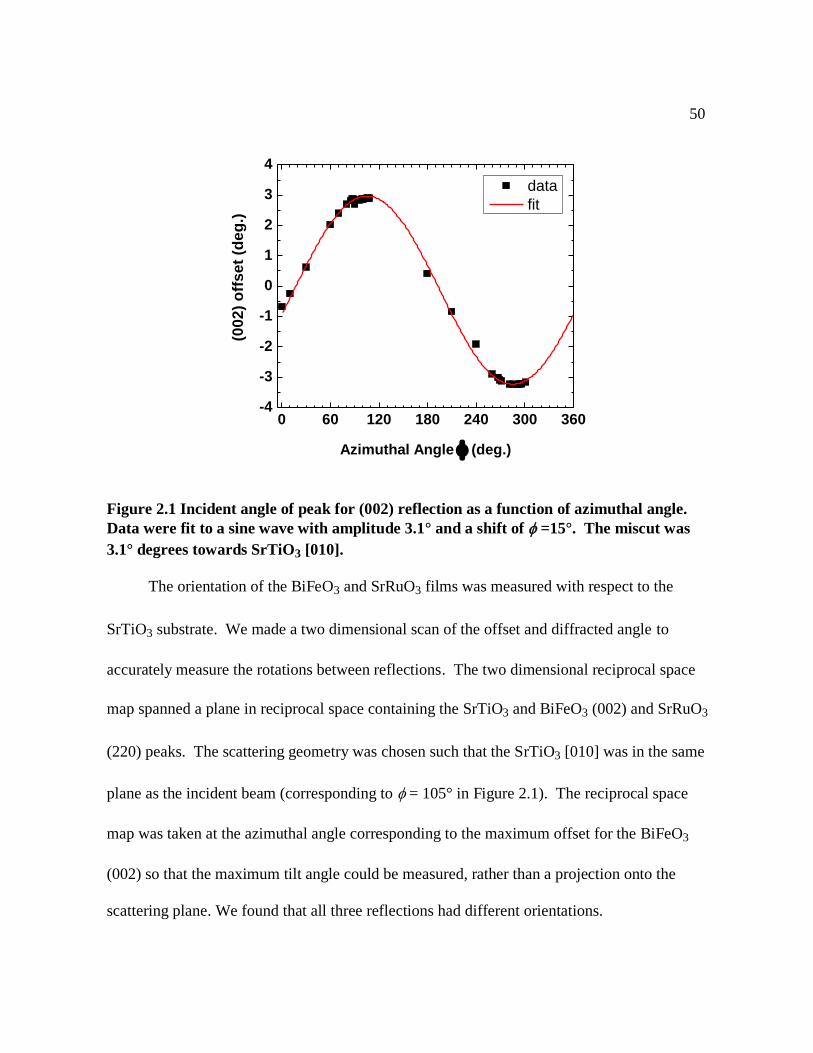
50
Figure 2.1 Incident angle of peak for (002) reflection as a function of azimuthal angle.
Data were fit to a sine wave with amplitude 3.1° and a shift of =15°. The miscut was
3.1° degrees towards SrTiO3 [010].
The orientation of the BiFeO3 and SrRuO3 films was measured with respect to the
SrTiO3 substrate. We made a two dimensional scan of the offset and diffracted angle to
accurately measure the rotations between reflections. The two dimensional reciprocal space
map spanned a plane in reciprocal space containing the SrTiO3 and BiFeO3 (002) and SrRuO3
(220) peaks. The scattering geometry was chosen such that the SrTiO3 [010] was in the same
plane as the incident beam (corresponding to = 105° in Figure 2.1). The reciprocal space
map was taken at the azimuthal angle corresponding to the maximum offset for the BiFeO3
(002) so that the maximum tilt angle could be measured, rather than a projection onto the
scattering plane. We found that all three reflections had different orientations.
0 60 120 180 240 300 360-4
-3
-2
-1
0
1
2
3
4
data
fit
(00
2)
off
se
t (d
eg
.)
Azimuthal Angle (deg.)

51
Figure 2.2. Area-averaged reciprocal space map of the BiFeO3 (002), SrRuO3 (220), and
SrTiO3 (002) at 8.05 keV. The offset angle is normalized to zero degrees at the SrTiO3
(002).
Rotations of the SrRuO3 and BiFeO3 layers were measured from the reciprocal space
map of the SrTiO3 (002), BiFeO3 (002), and SrRuO3 (220) reflections (Figure 2.2). Both the
SrRuO3 and BiFeO3 (002) reflections are rotated from the SrTiO3 (002), as shown
schematically in the inset of Figure 2.2. The SrRuO3 reflection is rotated by 0.057° from the
substrate reflection away from the sample surface. A more accurate value of the SrRuO3
orientation can be obtained by recording the difference in offsets of SrRuO3 and SrTiO3 peak
maxima when the miscut direction is in the scattering plane, repeating the measurement after
rotating the azimuthal angle 180°, and taking the average. This was 0.053. The offset for

52
the BiFeO3 reached a maximum when the miscut direction lay in the scattering plane as in
Figure 2.2, meaning that the BiFeO3 tilt direction was parallel to the miscut of the substrate.
The BiFeO3 (002) was rotated in the opposite direction, by 0.073° from the substrate, a total
of 0.13° from the underlying SrRuO3 film. The BiFeO3 and SrRuO3 layers were rotated by
different mechanisms, both of which are discussed in the following sections.
2.3.2. SrRuO3 rotation by expansion at step edges
The rotation of the SrRuO3 film can be described by a simple model of elastic
relaxation at step edges. Nagai observed this effect in GaInAs films on GaAs substrates,18
and explained it based on the insight that the film is clamped to the substrate at step edges,
where it is forced to have the same out-of-plane lattice constant as the substrate. At the edge
of a terrace, however, there is no clamping effect and the film can take on an elastically
relaxed lattice constant. This lattice constant can be predicted using the in-plane compression
of the film enforced by the substrate (aSTO = 3.905 Å) and assuming a Poisson‟s ratio of
0.3.19,7
Nagai‟s model, sometimes called the “step-edge expansion model,” is illustrated for a
compressively strained film in Figure 2.3.
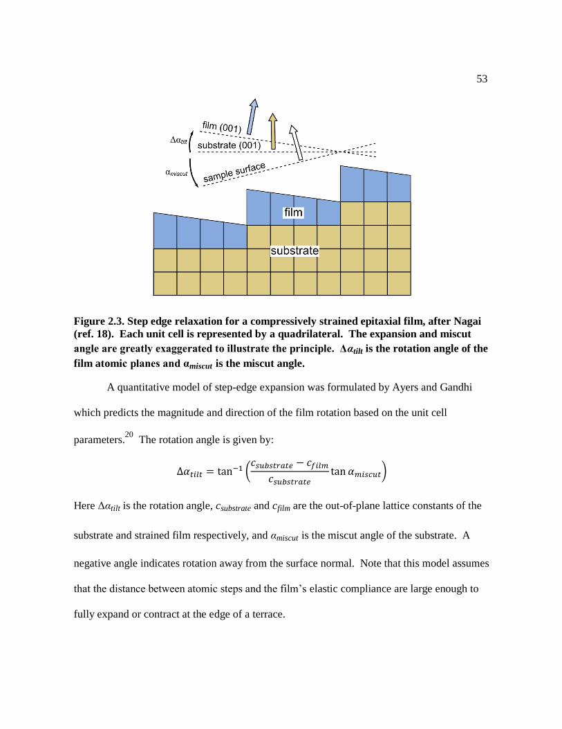
53
Figure 2.3. Step edge relaxation for a compressively strained epitaxial film, after Nagai
(ref. 18). Each unit cell is represented by a quadrilateral. The expansion and miscut
angle are greatly exaggerated to illustrate the principle. Δαtilt is the rotation angle of the
film atomic planes and αmiscut is the miscut angle.
A quantitative model of step-edge expansion was formulated by Ayers and Gandhi
which predicts the magnitude and direction of the film rotation based on the unit cell
parameters.20
The rotation angle is given by:
(
)
Here Δαtilt is the rotation angle, csubstrate and cfilm are the out-of-plane lattice constants of the
substrate and strained film respectively, and αmiscut is the miscut angle of the substrate. A
negative angle indicates rotation away from the surface normal. Note that this model assumes
that the distance between atomic steps and the film‟s elastic compliance are large enough to
fully expand or contract at the edge of a terrace.

54
The step-edge expansion model accurately describes the rotation of the SrRuO3 layers
in Figure 2.2. Using a pseudocubic out-of-plane lattice constant of cSRO = 3.97 Å for the film,
a bulk SrTiO3 lattice constant of csubstrate = 3.905 Å, and the measured miscut angle of 3.1°,
the predicted rotation for SrRuO3 on SrTiO3 is -0.050°. The observed rotation is -0.053°. The
observed rotation is thus in excellent agreement with the predicted value, both in direction
and magnitude.
The step-edge expansion model does not explain the rotation of the BiFeO3 film. From
the reciprocal space map in Figure 2.2, we found that the out-of-plane BiFeO3 lattice constant
was cBFO = 3.99 Å. When we use cSRO= 3.97 Å for the substrate lattice constant, the predicted
rotation is Δα = -0.015°. The observed angle between the BiFeO3 and SrRuO3 was +0.135°.
The step edge expansion model is not even qualitatively correct and cannot be responsible for
the BiFeO3 rotation.
2.3.3. BiFeO3 rotation caused by anisotropic defect nucleation
The disparity between the observed and predicted elastically induced rotations of the
BiFeO3 thin film lead us to consider other mechanisms that could be responsible for the
tilting. As noted by Ayers and Gandhi, the step relaxation model assumes the film is
pseudomorphic and that there is no relaxation via the introduction of misfit dislocations.20
Elasticity theory predicts an out-of-plane lattice constant of BiFeO3 in a pseudomorphic
elastically strained film on SrTiO3 would be 4.14 Å, assuming an in-plane lattice constant
equal to SrTiO3 (3.905 Å) and a Poisson ratio of 0.3. The measured value is c = 3.99 Å,

55
which is between the bulk and pseudomorphic constants. The epitaxial strain is thus partially
relaxed. We show here that the dislocation mechanism responsible for the relaxation is what
rotates the film.
We tested the hypothesis that the rotation of the BiFeO3 results from preferential
nucleation of dislocations in response to shear stresses. This effect was discovered in
epitaxial SiGe on miscut Si (001) substrates.21
Relaxation in SiGe occurs by nucleation of
defects at the film surface which glide along the {111} planes to the film-substrate
interface.22,23
These dislocations have Burgers vectors along ½ <101> directions. The
component of the dislocation parallel to the film-substrate interface reduces the strain energy
stored in the film, which in this case is the [100] or [010] direction.
Figure 2.4 Components of dislocations relaxing an epitaxial thin film on a miscut
substrate, after Mooney et al., ref.21. The Burgers vectors b1 and b2 can be decomposed
into bmisfit and btilt. The component bmisfit results from the projection of the Burgers
vector onto the epitaxial stress applied to the film and is the component which relaxes
the film. btilt rotates the (001) planes of the film. The misfit component of b2 is larger
than that of b1, so that dislocations with Burgers vector b2 are preferentially nucleated.

56
Two of the Burgers vectors b that can relax a compressively strained film are labeled
b1 and b2 in Figure 2.4. Each has a misfit component bmisfit, relaxing shear stress in the film,
and a component btilt that rotates (001) planes. On a miscut substrate there is a larger
resolved shear stress on one of the two slip systems because the stress lies in the plane of the
average surface rather than in the (001) plane. The activation energy for nucleating
dislocations decreases with stress parallel to b, so one of the slip systems is preferentially
nucleated. Tilt components of the preferred slip system for the compressively strained
BiFeO3 on SrTiO3 system, b2 in Figure 2.4, rotate BiFeO3 towards the surface normal. The
situation would be reversed for films under tensile stress, leading to rotations in the opposite
direction.
The dislocations necessary for the relaxation mechanism of ref. 21 have been
observed in epitaxial perovskite thin films. Dislocations with a [011_
] Burgers vectors would
simultaneously relax the misfit strain and rotate the BiFeO3 layer in the observed direction.
Dislocations in this family have been observed in other perovskite films on SrTiO3. Oh et al.
found misfit dislocations in SrRuO3 films on SrTiO3 substrates with <101> type Burgers
vectors,24
and Stemmer et al. observe stacking fault dislocations with b = ½ <101> in PbTiO3
films on SrTiO3 substrates.25
We believe b = [011_
] defects could be nucleated preferentially
by the anisotropic stress and rotate the film, as in the SiGe system. Preferential nucleation on
a miscut substrate leads to an overall tilt towards the surface normal in compressively strained
films, in agreement with experimental observations.

57
The magnitude of the tilt produced by preferential nucleation of defects cannot be
easily predicted. The tilt angle depends on the density of defects in the film, the dynamics of
defect propagation through the film, and their rate of nucleation. The biggest challenge is
quantifying the dynamics, since they depend on the energy required to nucleate a defect, the
growth temperature, epitaxial strain as a function of temperature, among other factors.26
The
dynamics of defect motion are complicated, making it difficult to predict the amount of
rotation of the film.
2.4. Mosaic block rotation
Probing smaller regions of the film with a focused beam gives information that a large
beam cannot. The large-beam diffraction pattern is the average structure of the entire film.
On the local scale, the film is broken up into mosaic blocks which each have different
orientations. When the scattering volume includes many mosaic blocks, the variation in
mosaic block orientations broadens x-ray reflections. This broadening makes it difficult to
observe more subtle features of the diffraction pattern, such as structural differences between
ferroelectric domains. Rather than averaging over many orientations, we used a focused x-
ray beam to study small regions of the film to avoid the reflection-broadening problem.
Synchrotron x-ray microdiffraction was used to image mosaic blocks and measure
their orientation. The (002) intensity was mapped over an area of the sample and reciprocal
space maps were taken in multiple places. Figure 2.5 (a) is a real space map of the BiFeO3
(002) reflection in a 10 m × 10 μm region of the sample. The diffractometer was aligned to
the maximum intensity of the BiFeO3 (002) reflection at the position marked 1 and the

58
sample was scanned underneath the focused beam. High intensity corresponds to regions in
which the (002) planes have the same interplanar spacing and orientation as at position 1.
Low intensity regions have different orientations than the region at position 1.
Figure 2.5 (a) X-ray microdiffraction image of mosaic blocks using the (002) reflection
of BiFeO3, acquired with diffractometer angles held at the maximum intensity in the
area marked 1. (b), (c) Reciprocal space maps taken at positions 1 and 2 on the surface
at 11.5 keV.
The orientations of two mosaic blocks were determined by acquiring reciprocal space
maps of the (002) reflections. Reciprocal space maps were taken at the positions labeled 1
and 2 within the microdiffraction map and are shown in Figure 2.5 (b) and Figure 2.5 (c),

59
respectively. There is a 0.15° rotation between (002) planes at position 1 and 2. Although the
maxima of the peaks appear at different incident angles, the total magnitude of the reciprocal
space vector is the same at both positions. The d-spacing of the planes is the same, but the
planes have been rotated with respect to each other. Furthermore, the reflections from regions
1 and 2 are part of the larger diffraction pattern in Figure 2.2. These are signatures of mosaic
blocks. In this film the mosaic blocks are on the order of 1μm across.
These diffraction patterns indicate that the orientation of the film is inhomogeneous at
the micron scale. The film as a whole is rotated on average by 0.13° with respect to the
SrRuO3 immediately beneath it, but there is an addition random rotation for each mosaic
block. A second important observation is that, despite this inhomogeneity, we find that there
is always only one (002) reflection within the scattering volume. If the focused beam were
bigger, then we would observe two or more reflections from multiple mosaic blocks. Within
this scattering volume there is only one orientation of the (001). Any ferroelectric domains
within the scattering volume have unit cells with parallel (001) planes, which was relevant in
determining domain patterns.
2.5. Strained stripe domains within mosaic blocks
Determining the domain pattern is important because of its importance to the
conductivity, switching dynamics, and magnetic properties of BiFeO3. X-ray diffraction
patterns provide information about the ferroelectric domain structure by using the structural
signatures of the polarization domains. The domain pattern can be inferred from (002) and
{103} diffraction patterns obtained with the focused beam. We observed a single (002)
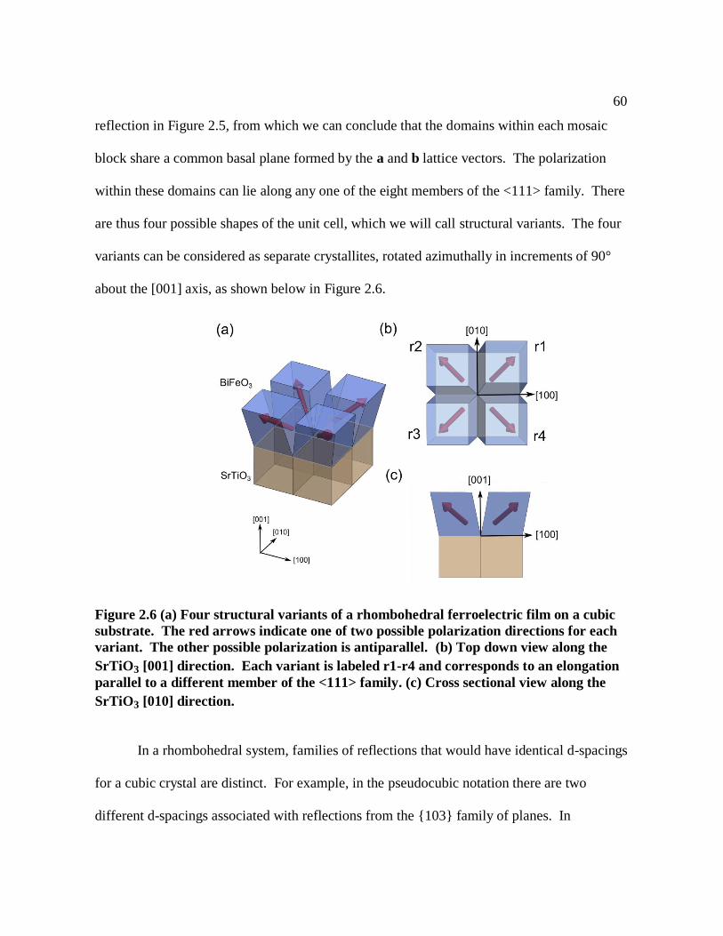
60
reflection in Figure 2.5, from which we can conclude that the domains within each mosaic
block share a common basal plane formed by the a and b lattice vectors. The polarization
within these domains can lie along any one of the eight members of the <111> family. There
are thus four possible shapes of the unit cell, which we will call structural variants. The four
variants can be considered as separate crystallites, rotated azimuthally in increments of 90°
about the [001] axis, as shown below in Figure 2.6.
Figure 2.6 (a) Four structural variants of a rhombohedral ferroelectric film on a cubic
substrate. The red arrows indicate one of two possible polarization directions for each
variant. The other possible polarization is antiparallel. (b) Top down view along the
SrTiO3 [001] direction. Each variant is labeled r1-r4 and corresponds to an elongation
parallel to a different member of the <111> family. (c) Cross sectional view along the
SrTiO3 [010] direction.
In a rhombohedral system, families of reflections that would have identical d-spacings
for a cubic crystal are distinct. For example, in the pseudocubic notation there are two
different d-spacings associated with reflections from the {103} family of planes. In

61
diffraction patterns, we can thus find several reflections from BiFeO3 at each of the reciprocal
space locations where we would have a single cubic reflection. The diffraction condition for
the (103) of variant r1 is very close that of the (013) of another variant, r2, because the
BiFeO3 unit cell is very close to a cube. By taking a large reciprocal space map, the Bragg
conditions can be met in turn for reflections from all of the variants present in the diffraction
volume.
To eliminate the problem of mosaic spread obscuring multiple peaks, we used x-ray
microdiffraction to probe a small area rather than the average of the entire film. In
experiments with larger, millimeter-scale x-ray beams, the mosaic spread broadened the
{103} reflections so much that it was not possible to distinguish between reflections from
different variants. The focused x-ray beam probed a diffraction volume containing one or
two mosaic blocks, compared to millions of mosaic blocks probed by a millimeter-sized
beam. X-ray microdiffraction made it possible to accurately determine angles between
multiple reflections.
2.5.1. BiFeO3 {103} reflections
We probed the in-plane structure and determined the ferroelectric domain pattern from
microdiffraction patterns of the {103} BiFeO3 reflections. A real space map of the BiFeO3
{103} intensity was acquired to determine the size of the ferroelectric domains. The real-
space map shown in Figure 2.6(a) was obtained by holding the diffraction conditions constant
while scanning the sample underneath the focused beam. The angles of the incident and
outgoing beams with respect to the sample were fixed at the maximum of the strongest

62
BiFeO3 {103} reflection at the point labeled 1 in Figure 2.7(a). Regions of high intensity
have the same lattice constant and orientation as at position 1. The incident angle for the
BiFeO3 pseudocubic {103} reflections was approximately 44°, leading to a beam footprint of
400 nm × 275 nm.
Figure 2.7 Microdiffraction image using the BiFeO3 {103} reflections at 2θ = 50.73° at
the area marked 1. Reciprocal space maps taken at positions 1 (b) and 2 (c) on the
surface.
There are multiple ferroelectric domains in each mosaic block. There is more than
one BiFeO3 reflection near the SrTiO3 (103), which shows that multiple structural variants
were present in the scattering volume. Reciprocal space maps acquired at the points labeled 1
and 2 are shown in Figure 2.7(b) and (c). The reciprocal space maps in Figure 2.7(b) and (c)

63
show at least two or three BiFeO3 reflections, respectively. This indicates that there are
regions within the scattering volume which have different lattice spacings and orientations
with respect to the substrate. The SrRuO3 and SrTiO3 (103) reflections are on the right side
of the figures and have sharp peaks indicating uniform interplanar spacing. The width of the
BiFeO3 reflections is increased by the complicated strain state imposed by incomplete
relaxation of epitaxy with the substrate. The presence of multiple BiFeO3 {103} peaks are a
signature of multiple polarization domains within a single mosaic block.
The rotations between multiple mosaic blocks within the diffraction volume could have
produced a number of reflections. The diffraction pattern of each block would be rotated
about the origin in reciprocal space and multiple Bragg reflections at all of the reciprocal
lattice vectors. However, we have consistently observed a single (002) reflection with the
focused beam. The diffraction volume in the film was smaller for the (002) than for the (103),
making it more likely to observe splitting in the (002). Therefore, we do not believe that
mosaic block rotation is responsible for the presence of multiple BiFeO3 {103} reflections in
each location.
2.5.2. Strained rhombohedral stripe domain pattern
The ferroelectric domain structure of BiFeO3 was determined by comparing our
microdiffraction results to predictions for domain patterns of a ferroelectric rhombohedral
film on a cubic substrate. Streiffer et al. calculated the minimum energy configuration for a
model ferroelectric rhombohedral film on a cubic substrate and found that the total strain
energy was reduced by forming a striped domain pattern.27

64
Streiffer et al. identified all possible domain walls by determining planes for which
two domains have identical electrostrictive displacement. After transforming from the high-
temperature paraelectric cubic phase to the ferroelectric rhombohedral phase the domains are
displaced by electrostrictive forces. By calculating the energy required to deform
rhombohedral domains to epitaxially conform to the substrate, the strain energy can be
obtained. The strain energy is modeled by what has been referred to as coherency defects.
Coherency defects are edge dislocations which account for the misfit strain. Screw
dislocations shear the unit cell to make a 90° angle between a and b lattice vectors. The
electronic contributions from the polarization were considered, and domain patterns which
did not have electrically neutral domain walls could be eliminated. These criteria were used
to identify geometric configurations of ferroelectric domains with the lowest possible strain
and electrostatic energies.
The ferroelectric domain patterns that minimize all of these energies have several
characteristics. The patterns consist of alternating stripes of two polarizations. Both
polarization domains are epitaxially constrained by the substrate. There is a 71° angle
between polarization vectors of neighboring domains in four of the patterns. 71° stripe
domain patterns have been observed in similar BiFeO3 (001) films using PFM.28,29
In these
particular patterns, the domains share a common (001) plane. This is consistent with the
(002) diffraction pattern observed in Figure 2.5.
The rhombohedral stripe domain model was used to predict which reflections could be
observed at the reciprocal space locations of the BiFeO3 {103} reflections. In the model
domain pattern we propose, the r1, r2, r3, and r4 structural variants have a shared set of (001)

65
planes. To predict the diffraction pattern of this configuration, we calculated the wavevectors
q corresponding to x-ray reflections from each variant. This was done for two models; a
monoclinic state as would occur in a pseudomorphic, unrelaxed film and a strained
rhombohedral state found in partially relaxed film. Neither model proposes new phases of
BiFeO3. Instead these model test different strained non-equilibrium states of the
rhombohedral phase.
First, we tested the monoclinic model described by Streiffer et al.27
This model
assumes that the film is strained into a metastable monoclinic structure. We calculated the
reciprocal lattice vectors for all four variants of a fully coherent film within one mosaic block
and compared the predicted values to the three dimensional reciprocal space map of the {103}
reflections shown in Figure 2.8. We used a monoclinic MC structure (in which the c lattice
vector is rotated in the (110) plane) with lattice constants a = b = 3.905Å, c = 3.99Å, and
monoclinic tilt angle 0.6° to calculate the reciprocal lattice vectors. Two sets of variants
produced reflections at the same reciprocal space vectors so the r1 (103) and r4 (013) have
q{103} = (1.609, 0, 4.712), while the r2 (0-13) and r3 (-103)
have q{103} = (1.609, 0, 4.736). The in-plane components of the predicted
reflections do not match those observed in a three dimensional reciprocal space map of the
(103) reflection. Moreover, there is no way for two variants with monoclinic symmetry in a
coherent block to be split in qy as found experimentally in Figure 2.8 (b). The monoclinic
model is incorrect because the film is not coherent.

66
Figure 2.8. Three dimensional reciprocal space map of the SrTiO3, SrRuO3, and BiFeO3
{103} reflections projected onto the (a) qx-qz plane and (b) the qy-qz plane.
A relaxed rhombohedral stripe domain model gave insight into the domain pattern.
The peak splitting observed in Figure 2.8 is consistent with relaxed stripe domains. Models
in which the angle between the pseudocubic a and b lattice vectors is less than 90° fit the
splitting of the {103} quite well. After lifting this constraint there were too many variables to
uniquely solve the structure and identify the exact structural variant based solely on the {103}
reciprocal space map. Only triclinic models were able to match the observed pattern exactly.
. We examined a series of rhombohedral and triclinic models with different lattice
constants and discovered they shared an important trend. For all tested structures, the
reciprocal lattice vectors for the r1 (103) and r4 (013) reflections always have a larger
magnitude than those of the r2 (01_
3) and r3 (1_
03) reflections. The peak labeled BFO 2 can be
assigned to either r1 or r4, and r2 or r3 to BFO 1. All of the four possible variant

67
combinations are consistent with the 71° stripe domain pattern discussed above. Therefore
we conclude that these films contain the stripe domains in Streiffer et al. which have been
anisotropically strained into a triclinic state.
2.6. Conclusions
Epitaxial BiFeO3 (001) films grown on miscut substrates undergo anisotropic
relaxation. The anisotropy in stress applied to the film causes anisotropic nucleation of
defects, destroying the in-plane symmetry as well as resulting in a net rotation of the entire
film. X-ray microdiffraction further shows the presence of multiple structural domains within
individual mosaic blocks. The splitting of off-specular reflections were compared with
predicted scattering from 71° rhombohedral stripe domains which share {101} type domain
walls.
These results are consistent with strained rhombohedral stripe domains. As the
epitaxial strain is relaxed via the introduction of defects, BiFeO3 films return to the
equilibrium rhombohedral symmetry. Unrelaxed (001) BiFeO3 films are strained into
monoclinic symmetry by the epitaxial stress of the substrate.6 Partially relaxed films like the
ones studied here have triclinic symmetries somewhere between monoclinic and
rhombohedral. BiFeO3 films with different symmetries are not new thermodynamic phases,
just variations in the degree of epitaxial strain.
68
2.7. Chapter 2 references
1 J. Wang, J. B. Neaton, H. Zheng, V. Nagarajan, S. B. Ogale, B. Liu, D. Viehland, V.
Vaithyanathan, D. G. Schlom, U. V. Waghmare, N. A. Spaldin, K. M. Rabe, M. Wuttig, and
R. Ramesh, “Epitaxial BiFeO3 multiferroic thin film heterostructures,” Science 299, 1719
(2003).
2 G. Xu, J. Li, and D. Viehland, “Ground state monoclinic (M-b) phase in (110)(c) BiFeO3
epitaxial thin films,” Appl. Phys. Lett. 89, 222901 (2006).
3 S. Geprägs, M. Opel, S. T. B. Goennenwein, and R. Gross, “Multiferroic materials based on
artificial thin film heterostructures,” Philos. Mag. Lett. 87, 141 (2007).
4 K. Saito, A. Ulyanenkov, V. Grossmann, H. Ress, L. Bruegemann, H. Ohta, T. Kurosawa, S.
Ueki, and H. Funakubo, “Structural Characterization of BiFeO3 Thin Films by Reciprocal
Space Mapping," Jpn. J. Appl. Phys. Part 1 45, 7311 (2006).
5 R. J. Zeches, M. D. Rossell, J. X. Zhang, A. J. Hatt, Q. He, C. H. Yang, A. Kumar, C. H.
Wang, A. Melville, C. Adamo, G. Sheng, Y.–H. Chu, J. F. Ihlefeld, R. Erni, C. Ederer, V.
Gopalan, L. Q. Chen, D. G. Schlom, N. A. Spaldin, L. W. Martin, and R. Ramesh, “Ground
state monoclinic (M-b) phase in (110)(c) BiFeO3 epitaxial thin films,” Science 326, 977
(2009).
6 G. Xu, H. Hiraka, G. Shirane, J. Li, J. Wang, and D. Viehland, “Low symmetry phase in
(001) BiFeO3 epitaxial constrained thin films,” Appl. Phys. Lett. 86, 182905 (2005).
7 M. D. Biegalski, K. Dörr, D. H. Kim, and H. M. Christen, “Applying uniform reversible strain
to epitaxial oxide films,” Appl. Phys. Lett. 96, 151905 (2010).
8 H. Liu, P. Yang, K. Yao, and J. Wang,“Twinning rotation and ferroelectric behavior of
epitaxial BiFeO3 (001) thin film,” Appl. Phys. Lett. 96, 012901 (2010).
9 Q. Gan, R. A. Rao, and C. B. Eom, “Control of the growth and domain structure of epitaxial
SrRuO3 thin films by vicinal (001) SrTiO3 substrates,” Appl. Phys. Lett. 70, 1962 (1997).
10 R. A. Rao, Q, Gan, and C. B. Eom, “Growth mechanisms of epitaxial metallic oxide SrRuO3
thin films studied by scanning tunneling microscopy,” Appl Phys. Lett. 71, 1171 (1997).
11 H. W. Jang, D. Ortiz, S. H. Baek, C. M. Folkman, R. R. Das, P. Shafer, Y. Chen, C. T.
Nelson, X. Pan, R. Ramesh, and C. B. Eom, “Domain engineering for enhanced ferroelectric
properties of epitaxial (001) BiFeO3 thin films,” Adv. Mater. 21, 817 (2009).

69
12
R. R. Das, D. M. Kim, S. H. Baek,, C. B. Eom, F. Zavaliche, S. Y. Yang, R. Ramesh, Y. B.
Chen, X. Q. Pan, X. Ke, M. S. Rzchowski, and S. K. Streiffer, “Synthesis and ferroelectric
properties of epitaxial BiFeO3 thin films grown by sputtering,” Appl. Phys. Lett. 88, 242904
(2008).
13 Seidel, J. et al. “Conduction at domain walls in oxide multiferroics,” Nature Mater. 8, 229
(2009).
14 Y. B. Chen, M. B. Katz, X. Q. Pan, R. R. Das, D. M. Kim, S. H. Baek, and C. B.
Eom,“Ferroelectric domain structures of epitaxial (001) BiFeO3 thin films,” Appl. Phys. Lett.
90, 072907 (2007)
15 L. W. Martin, et al. “Nanoscale control of exchange bias with BiFeO3 thin films,” Nano
Lett. 8, 2050 (2008).
16 S. F. Liu, S. E. Park, H. Lei, L. E. Cross, T. R. Shrout,”E-field dependence of piezoelectric
properties of rhombohedral PZN-PT single crystal,” Ferroelectrics 221, 169 (1999).
17 B. E. Warren, X-ray Diffraction, (Dover Publications, New York, 1990).
18 H. Nagai, “Structure of vapor deposited GaxIn1-xAs crystals,” J. Appl. Phys. 45, 3789
(1974).
19 C. Ederer and N. A. Spaldin,“Effect of epitaxial strain on the spontaneous polarization of
thin film ferroelectrics,” Phys. Rev. Lett. 95, 257601 (2005).
20 J. E. Ayers and S. K. Ghandhi, “Crystallographic tilting of heteroepitaxial layers,” J. Cryst.
Growth 113, 430 (1991).
21 P. Mooney, F. K. LeGoues, J. Tersoff, and J. O. Chu, “Nucleation of dislocations in SiGe
layers grown on (001),” J. Appl. Phys. 75, 3968 (1994).
22 M. A. Capano, “Multiplication of dislocations in Si1-xGex layers on Si(001),” Phys. Rev. B
45, 768 (1992).
23 C. J. Gibbings, C. G. Tuppen, and M. Hockly, “Dislocation nucleation and propagation in
Si0.95Ge0.05 layers on silicon,” Appl. Phys. Lett. 54, 148 (1989).
24 T. Suzuki, Y. Nishi, and M. Fujimoto, “Analysis of misfit relaxation in heteroepitaxial
BaTiO3 thin films,” Phil. Mag. A 79, 2461 (1999).
25 S. Stemmer, S. K. Streiffer, F. Ernst, and M. Rühle, “Dislocations in PbTiO3 thin-films,”
Phys. Stat. Sol. A 147, 135 (1995).

70
26
E.P. Popov, Introduction to Mechanics of Solids (Prentice-Hall, 1968)
27 S. K. Streiffer and C. B. Parker, “Domain patterns in epitaxial rhombohedral ferroelectric
films. I. Geometry and experiments” J. Appl. Phys. 83, 2744 (1998).
28 F. Zavaliche, R. R. Das, D. M. Kim, C. B. Eom, S. Y. Yang, P. Shafer and R. Ramesh,
“Ferroelectric domain structure in epitaxial BiFeO3 films,” Appl. Phys. Lett. 87, 182912
(2005)
29 Y. -H. Chu, M. P. Cruz, C. -H. Yang, L. W. Martin, P .-L. Yang, J. -X. Zhang, K. Lee, P.
Yu, L. -Q. Chen, and R. Ramesh, “Domain control in multiferroic BiFeO3 through substrate
vicinality,” Adv. Mater. 19, 2662 (2007).
71
Chapter 3. X-ray Diffraction Signatures of Ferroelectric
Polarization
The intensity of x-ray diffraction reflections in ferroelectric materials depends on the
polarization direction. In fact, this change in intensity can be used to image ferroelectric
domains.1 In order to exploit this phenomenon, however, it is necessary to understand the
origin of the intensity change. Kinematic scattering models predict changes in diffracted
intensity originating from the change in atomic positions when the ferroelectric polarization is
switched. For perovskite materials which are ferroelectric, the change is predicted to be
several percent of the Bragg reflection intensity. Previous studies in other groups have
observed intensity changes up to a few percent of the intensity in BaTiO3 thin films, which fit
the kinematic models quite well.2 Do et al., in previous work within our research group, have
previously observed large changes of up to 30% in the intensity of the (002) reflection of
Pb(Zr,Ti)O3 (PZT) thin films when the direction of the polarization is changed. 3,4
Calculating the structure factor for PbTiO3, a ferroelectric with a structure similar to PZT,
gives an intensity contrast of 5 to 10%, far less than the experimental observation.4 Based on
the success of the kinematic scattering model with BaTiO3, we theorized that with slight
modifications the model could accurately predict the scattering from PZT films as well.
Discrepancies between the predicted and experimental intensities were used to refine the
kinematic scattering model. In the process, we improved our understanding of the structure
of PZT films.

72
Refining the kinematic scattering model for PZT is also relevant to BiFeO3. We
observe intensity changes of 20% to 30% upon polarization switching in BiFeO3 films,
similar to PZT (001) films. Unlike PZT, BiFeO3 (001) films have a complex structure as seen
in Chapter 2, making it difficult to determine atomic positions accurately. Furthermore, when
an electric field is applied along the [001]pc direction, the ferroelectric polarization switches
to one of four possible directions. The uncertainty in atomic positions and multiple switching
paths makes it extremely difficult to accurately predict the change in intensity of BiFeO3
reflections after polarization switching.
Compared to BiFeO3, PZT has a simple structure. At compositions far from the
morphotropic phase boundary near x=0.5 PZT has a well-defined rhombohedral or tetragonal
structural state at room temperature.5 Tetragonal PZT, which occurs for compositions with x
< 0.50, has a polarization parallel to the c axis of the unit cell. It is possible to deposit
epitaxial films of tetragonal PZT on (001) SrTiO3 substrates which have the c axis of the unit
cell along the surface normal. The polarization in tetragonal PZT thin films of this type is
constrained to be along one of only two polarization directions; it can be either parallel or
antiparallel to the surface normal. When an electric field above the coercive field Ec is
applied, there is only one stable polarization direction, making comparisons to intensity
calculations for a single (hkl) reflection straightforward.
We hypothesize that the polarization-dependent intensity contrast is caused by similar
phenomena for PZT and BiFeO3. Both materials are perovskite ferroelectrics. Both are
compressively strained epitaxial thin films. The Bi3+
or Pb2+
cations in BiFeO3 and PZT have

73
similar ionic radii and unbonded lone pairs.6 The structural similarities between BiFeO3 and
PZT lead us to believe that the intensity change upon polarization switching is likely to have
similar origins in both materials. Thus, in order to determine the origin of the large intensity
contrast in BiFeO3 and simultaneously solve an open question about previous work, we
studied the polarization-dependent intensity of the structurally simpler material, PZT.
Our hypothesis was that the atomic positions, scattering factors, or long range
ordering assumed in the kinematic scattering model were incorrect, making the predicted
intensities inaccurate. The key issue involved in simulating the diffraction patterns accurately
is to account for these phenomena quantitatively. We tested several variations of the structure
which could in principle lead to the large intensity contrast observed experimentally. One
possible origin of this difference is inaccurate knowledge of the atomic positions within the
PZT unit cell. The intensity contrast is sensitive to the distance between atoms, especially
those with large atomic scattering factors. Even small displacements of the Pb2+
or Zr4+
/Ti4+
ions change the intensity contrast. A second possibility is that the atomic scattering factors
of the atoms in PZT films differ from those used in the calculation. Because the intensity of a
Bragg reflection depends on the imaginary part of the atomic scattering factor, uncertainties
in these scattering factors can have a large impact on the results. The final possibility we
considered is that the Zr and Ti atoms have a structure with sufficient long-range order to
make the prediction inaccurate.
In order to determine the cause of the increased contrast between polarization domains
in PZT, we measured the intensity contrast as a function of energy for several different x-ray
reflections. Experimental results were compared to predictions from several kinematic

74
scattering models. First, the kinematic scattering from PbTiO3 was calculated to
qualitatively predict the intensity change for several reflections. The PbTiO3 model predicts a
sharp increase of the intensity contrast at absorption edges, so we focused on energies near
the Pb L3 edge at 13.035 keV. The intensities of several reflections were measured as a
function of polarization direction and photon energy. We observed an increased intensity
contrast at the Pb L3 edge as predicted. Comparison between experimental and predicted
intensities showed that the contrast depends on the distance between the Pb and Zr/Ti atoms
and the imaginary part of the atomic scattering factor.
3.1. Kinematic scattering from PbTiO3 : A qualitative prediction for PZT
intensity contrast
We hypothesized that the intensity contrast arises from the location of ions within the
Pb(Zr,Ti)O3 unit cell. These ions do not occupy centrosymmetric positions, and thus there
can be a difference between the intensities of reflections with opposite indices. This effect
has been used to determine the orientation of a non-centrosymmetric crystal using the
difference in intensities of (111) and (-1-1-1) reflections in a ZnS crystal.7 In these early x-
ray scattering experiments, the experimenters measured the intensity of reflections with
indices (111), rotated the crystal, and then measured the intensity of the (-1-1-1) reflection. In
terms of atomic positions, rotating the ZnS crystal is similar to switching the polarization
direction in a perovskite.

75
The same phenomenon can be used to determine the direction of the remnant
polarization in ferroelectric perovskites. We model the crystallographic effect of reversing
the direction of the polarization as being equivalent to inverting the crystal, so that the (hkl)
planes after polarization switching are equivalent to the (-h-k-l) planes before switching. In
order to predict the intensity contrast between polarization directions, we calculate the
difference in structure factors of the (hkl) and (-h-k-l) reflections as a function of energy for
several different planes.
3.1.1. Analytical expression for polarization-dependent intensity
The difference between the intensities of the (hkl) and (-h-k-l) reflections is predicted
by calculating their structure factors. The structure factor F depends on the scattering
wavevector q, the atomic positions within the unit cell rn, the wavevector dependent part of
the scattering factor f 0, and the energy dependent dispersion corrections to the real and
imaginary parts, f ' and f ", respectively. When q is equal to a reciprocal lattice vector ghkl, the
structure factor reduces to:
∑
where u, v, and w are the fractional indices of the atomic positions, such that
. In tetragonal materials with a 4-fold rotation about the c axis, h and k are
degenerate so there is no difference between the structure factors for the (hk-l) and (-h-k-l)
planes. The analytical expression for the difference in intensities can be found by subtracting
the structure factors for (hkl) and (-h-k-l) and simplifying the expression. For a unit cell with

76
n atoms, the difference in intensities is given by:
( ) ∑ ∑ [ ] [ ]
The difference in intensity depends on the imaginary parts of the atomic scattering
factors, the Miller indices of the particular reflection, and the atomic positions. The
argument of the sine function above is the phase difference between x-rays scattered from
atoms j and k. The difference in phase is caused by the difference in path lengths taken by x-
rays scattering from the two atoms.
There would be no difference between the (hkl) and (-h-k-l) intensities if the
imaginary part of the scattering factor were zero. There were two simple ways to test this
theory - altering h, k, and l by diffracting from several different planes, and varying f" by
changing photon energy.
3.1.2. PbTiO3 structure factor and definition of intensity contrast ratio
A framework for understanding energy dependence and sign of the intensity contrast
was given in section 3.1.1. We can apply this model first to PbTiO3 which has the same
symmetry as the PZT crystal we have studied extensively. PbTiO3 also has a simpler
structure than PZT because it includes only one type of central atom and it thus can be
described using a structure with a small unit cell that includes only single Pb and Ti atoms.
The PbTiO3 structure factor is calculated for two polarization states to predict the
intensity contrast ratio. The arrangements of atoms and the directions of the polarizations in
the two states are shown in Figure 3.1. The down polarization state (Pdown) has the

77
polarization pointing antiparallel to the c axis, towards the interface between the film and the
substrate. This state can be produced by applying a positive voltage to the top electrode of a
capacitor with the bottom electrode grounded. In a thin film diffraction experiment in which
the x-ray beam enters and exits through the surface of the thin film, the Pdown domain state
produces x-ray reflections with indices (hkl) in which l is positive. In the up polarization
state, Pup, the same x-ray scattering geometry produces reflections with negative values of l.
The Pup state can be reached with by applying a negative voltage to the top electrode.
Figure 3.1. PZT unit cell in the (a) polarization down and (b) polarization up states. The
central Ti/Zr atom and oxygen atoms change their positions along the c axis when the
polarization is switched.
Structure factor calculations for PbTiO3 were performed using atomic scattering
factors and atomic positions found in the literature. Atomic scattering factors fPb, fTi, and fO
were taken from Henke et al. and calculated using the XOP computer program.8,11
Atomic
positions for PbTiO3 were taken from Wyckoff.9 In order to quantify the contrast in intensity
between the Pup and Pdown states, we defined a ratio of intensities:
( ) ( )

78
This parameter is used to compare calculated and experimental values of the polarization
dependent intensity. The intensity ratio for several reflections was calculated as functions of
energy for comparison with experimental results.
3.1.3. Intensity ratio predictions
When there is no absorption of the x-ray photons by a crystal the scattering factors are
completely real and f’’ is zero. In this hypothetical case, the scattering factor F(hkl) is equal
to the complex conjugate of F(-h-k-l) and as a result the intensity given by FF* does not
change when all of the indices of the reflection change sign. This effect is known as Friedel‟s
Law, and it provides a useful rule of thumb. As a result of Friedel‟s Law reflections with
opposite indices have equal intensities even non-centrosymmetric crystals, as long as
absorption can be neglected. This premise breaks down as soon as f " becomes significant,
most noticeably near absorption edges.
The magnitude of the intensity contrast depends on the energy of the x-ray photons.
In a general sense, the intensities of Bragg reflections depend on the energy of the x-ray
photons because the dispersion corrections to the atomic scattering factor, f ' and f ", have
strong energy dependences. The imaginary part of the scattering factor, f ", is proportional to
the absorption cross section σa:
As a result, f " increases sharply at the absorption edges. The relationship between f ' and f "
can be described via the Kramers-Kronig relation:10

79
∫
( )
In practice, we can use tabulated values of the dispersion corrections to predict the atomic
scattering factors. Henke et al. provide tables of f ' and f " for elements with atomic numbers
1 to 92. 11
The increase in f " at absorption edges makes the intensity ratio largest at these photon
energies. We carefully studied the intensity ratio at energies near the Pb L3 absorption edge
for two reasons. First, the predicted rapid variation in ratio predicted by the model would be
easy to observe experimentally. Furthermore, the photon energies of absorption edges for the
other constituents of PZT have wavelengths that are either too large or too small for
microdiffraction experiments. The predicted intensity ratio is plotted as a function of energy
near the Pb L3 absorption edge is plotted Figure 3.2 for several reflections.
Figure 3.2. Qualitative prediction for intensity contrast ratio based on calculated values
of the energy dependent PbTiO3 structure factor.

80
The large jump in the magnitude of the ratio near 13 keV is caused by the increase in
the imaginary part of the scattering factor of Pb at the L3 absorption edge near 13.035 keV.
The intensity ratio is also strongly dependent on the distance between the Pb and Ti ions,
which affects the phase factor. This factor also depends on the difference in the imaginary
components of the Pb and Ti scattering factors.
In Figure 3.2, a positive ratio indicates that the diffracted intensity for the Pdown state
is more intense than in the Pup state. The sign of the ratio at these energies is determined by
the sum of Miller indices h, k, and l. When h+k+l is even, the reflection is more intense in
the Pdown state; when h+k+l is odd, the reflection is more intense in the Pup state. These sign
rules only apply for PbTiO3 at photon energies within several keV of the Pb L3 edge because
at photon energies near the Pb L3 edge the intensity ratio is dominated by the lead and
titanium f ".
3.2. Intensity contrast measurements
A series of measurements were designed to test the hypothesis that the polarization-
dependent variation in the intensity of x-ray reflections is solely the crystallographic location
of ions away from centrosymmetric positions. On the basis of the quantitative description
developed in the previous section, we could test that hypothesis with the following specific
predictions:

81
1) The Pdown has higher intensity than Pup for reflections with h+k+l=2n.
2) The Pup state has higher intensity than Pdown for reflections with h+k+l=2n+1
3) The magnitude of the intensity ratio will be maximized at photon energies near the
Pb L3 edge, 13.035 keV.
Based on these criteria, we measured the polarization dependent intensity for several
reflections as a function of the photon energy, for a range of energies near the Pb L3 edge.
The sample used in this study is an epitaxial thin film of (001) oriented
Pb(Zr0.45Ti0.55)O3 on an SrTiO3 substrate. This composition of PZT is tetragonal at room
temperature and has a large remnant polarization.12
A 100 nm-thick conducting SrRuO3 layer
between the PZT and the substrate acted as a bottom electrode. The PZT and SrRuO3 thin
films were deposited on a (001) SrTiO3 substrate using off-axis radio-frequency sputtering by
our collaborators in Prof. Chang-Beom Eom‟s group.13
Circular top electrodes with various
diameters from 25 μm to 200 μm were patterned by sputtering 20 nm of platinum on top of
the PZT through a shadow mask. We used capacitors with 100 μm diameter top electrodes
for these experiments. The out-of-plane lattice constants of the thin films were measured
with a θ-2θ scan along the substrate surface normal direction of reciprocal space, including
the SrTiO3 (002), PZT (002), and SrRuO3 (220) reflections.
We applied electric fields to capacitors to switch the ferroelectric polarization so we
could measure the x-ray scattering from a region with a known, uniform polarization. Top
electrodes were contacted with a high bandwidth 5µm tungsten probe tip (Cascade Microtech,
107-158). The SrRuO3 bottom electrode was contacted by soldering a thin platinum wire to

82
an area at the corner of the sample where the film had been removed to expose the SrRuO3
bottom electrode. This wire was connected to the outer coaxial connection of the probe tip.
Electric fields were applied to the region underneath the top electrode by applying a voltage
across the film thickness using a function generator (Agilent 33120A).
3.2.1. Microdiffraction experiments
The variation in the intensity of x-ray reflections of the PZT thin film was measured
using synchrotron microdiffraction. The focused beam was used to probe regions under
electrodes, each of which were uniformly poled. The intensity of each reflection was
measured after poling the capacitor by applying positive voltages to the top electrode, which
produced the Pdown state, and negative voltages, which lead to the Pup state. The ratio of these
intensities was computed from the data in order to compare with predictions from a PbTiO3
kinematic scattering model.
A focused, monochromatic x-ray beam was used for the microdiffraction experiments.
The x-ray beam was produced by a minigap undulator insertion device14
at beamline X13b of
the National Synchrotron Light Source (NSLS). The undulator had a gap of 3.3 mm and a
corresponding maximum intensity at 11.46 keV. A Si (111) monochromator was used to
select a monochromatic beam at various energies. The photon energy was calibrated at
11.103 keV using the Ge K edge absorption by measuring the drop in intensity with an
ionization chamber after the beam had passed through a Ge foil. During the course of the
experiment, the energy calibration was checked by measuring the x-ray fluorescence from
lead tape at the Pb L3 edge. The beam was focused using Kirkpatrick-Baez (K-B) mirrors to

83
a spot size of 10-20 μm.15
K-B mirrors were used because they are achromatic, and thus
their focal length does not change when the energy of the x-rays is varied.
Normalizing the diffracted signal to intensity variations in the incident beam was an
essential step in accurately comparing multiple intensity measurements. The main source of
variation in the incident beam came from the decay of the current inside the storage ring of
the synchrotron. Electrons in a storage ring are continuously lost from the stored beam,
leading effectively to a finite lifetime on the order of hours. This means that the current in the
ring (and therefore the intensity of x-rays being produced) is constantly decreasing unless
more electrons are injected into the ring. The current in the synchrotron storage ring at NSLS
was injected once every twelve hours after dumping the residual stored electron beam. The
beam current decreases significantly even over the course of an hour, so it is necessary to
monitor intensity of the incident beam in order to avoid artifacts in the experimental results.
This is commonly done by installing an ion chamber upstream of the diffractometer. In this
experiment, diffracted intensities were normalized to the readout from an ion chamber that
was placed in the hutch upstream from the sample, between the K-B mirrors.
The sample was mounted on a diffractometer in a vertical scattering geometry. The
K-B mirrors focused the x-ray beam at the center of rotation of the diffractometer. The
electrical probe tip was mounted on the diffractometer such that the tip could make contact
with the top electrodes of capacitors on the sample. The tip, sample, and bottom electrode
were set up to enable poling and hysteresis loop measurements of capacitors.
The diffracted beam was detected using a scintillation detector (Saint-Gobain,
Bicron). The scintillation detector produces a single voltage pulse for each detected photon,
84
with a pulse height pulse proportional to the photon energy. The detector output was
amplified and filtered using a single channel analyzer (SCA). We chose the SCA limits so
only photons that were elastically scattered were counted. High energy photons from higher
order harmonics of the undulator and low energy fluorescent photons were filtered out. The
particular scintillation detector we used produces pulses with poorly defined heights, with a
pulse-to-pulse variation of approximately 50% even for monochromatic photons. The SCA
thus provided efficient discrimination against higher harmonics, but did not efficiently reduce
the fluorescent noise from elements with edges just below the incident energy.
The angular resolution of the detector was set using slits placed directly in front of the
detector. The 10mm 6 mm slits were 36.8 cm from the sample and had an angular
acceptance of 0.93° in 2θ and 1.55° in the horizontal direction, which was perpendicular to
the scattering plane. This large acceptance allowed the integrated intensity of the reflection to
be measured.
3.2.2. X-ray fluorescence
X-ray fluorescence provided a way to determine where the x-ray beam was on the
sample. The fluorescent x-rays emitted from the sample were analyzed using a Si p-i-n diode
fluorescence detector (AMPTEK XR-100CR) and a multichannel analyzer (Amptek
MCA8000A). The presence or absence of fluorescent x-rays at energies corresponding to W,
Pt, and Pb determined whether the focused beam was striking the tungsten probe tip, a
platinum electrode, or the Pb(Zr,Ti)O3 film, respectively.
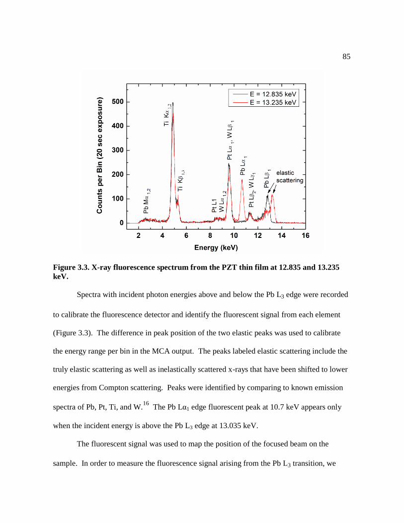
85
Figure 3.3. X-ray fluorescence spectrum from the PZT thin film at 12.835 and 13.235
keV.
Spectra with incident photon energies above and below the Pb L3 edge were recorded
to calibrate the fluorescence detector and identify the fluorescent signal from each element
(Figure 3.3). The difference in peak position of the two elastic peaks was used to calibrate
the energy range per bin in the MCA output. The peaks labeled elastic scattering include the
truly elastic scattering as well as inelastically scattered x-rays that have been shifted to lower
energies from Compton scattering. Peaks were identified by comparing to known emission
spectra of Pb, Pt, Ti, and W.16
The Pb Lα1 edge fluorescent peak at 10.7 keV appears only
when the incident energy is above the Pb L3 edge at 13.035 keV.
The fluorescent signal was used to map the position of the focused beam on the
sample. In order to measure the fluorescence signal arising from the Pb L3 transition, we

86
integrated the photons with energies arriving in a region of interest (ROI) between 10 keV
and 10.5 keV. The increase in Pb Lα1 fluorescence at the Pb L edge was used to recalibrate
the monochromator energy during the course of the experiment. The Pt Lα and W Lβ
transitions occur at nearly the same energies, so we defined an ROI which measured the sum
of Pt and W signal. The Pt and W fluorescence proved to be useful in finding the electrical
probe tip and capacitor top electrodes with the focused beam. Figure 3.4 shows the diffracted
intensity from the PZT (004) and the Pt/W fluorescent signal that were recorded
simultaneously as the sample was scanned underneath the beam.
Figure 3.4. PZT (004) diffracted intensity and Pb / W x-ray fluorescence map of a 100
µm capacitor and the probe tip.
The diffracted intensity and fluorescence provided complimentary information during
sample maps; the diffracted beam was attenuated by the probe tip and its shadow while the
fluorescence clearly showed the presence of the electrode. The Pt top electrode absorbed
some of the diffracted beam, but the intensity dependence on polarization direction and
photon energy was larger than the absorption decrease. The Pt fluorescence did not vary with

87
photon energy or polarization direction, making it a reliable indication of whether the beam
was on a capacitor.
3.2.3. Ferroelectric polarization switching
In order to measure the diffracted intensity from a well-defined polarization domain
configuration, the capacitors were poled by applying an electric field. We measured
ferroelectric hysteresis loops and used them to determine the coercive fields for this PZT film
to ensure the polarization was completely switched, as described in Section 1.7.2. Three
periods of a triangle waveform with an amplitude of 7 V and a frequency of 10 kHz were
applied to top electrodes with a diameters of 100μm. The coercive fields were +350 kV/cm
and -150 kV/cm. The apparent difference in coercive field is an effect of different materials
in the top and bottom electrodes.17
The remnant polarization measured from the hysteresis loops was used to estimate the
damage to the device. Exposure to intense x-rays can introduce electrical and structural
defects in ferroelectric thin films. The remnant polarization 2Pr = 93 μC/cm2 measured in
Figure 1.6 was used as a baseline. Typical values of Pr for an as-grown capacitor in this film
were around 40-45 μC/cm2, which closely matches literature values in films of similar
compositions (0.4 > x > 0.52) which range from 35µC/cm2 to 45µC/cm
2.18,19
Pr decreased
with the number of switching cycles and exposure to x-rays. We used the decrease in Pr as a
gauge for fatigue and beam damage during the course of the experiment.

88
The capacitors were poled immediately before measuring the x-ray reflection
intensity. The series of voltages in Figure 1.5 was used to measure Pr and to pole the
capacitor. Because the last triangular voltage pulse is negative this sequence leaves the
capacitor in the Pup state. Pulse trains with the same frequency and opposite polarity were
used to switch the polarization to the Pdown state. These pulses produced maximum
amplitudes of ±875 kV/cm, well above the coercive field, which was at most +350 kV/cm for
the positive direction.
3.2.4. Spatial average of intensity contrast
The intensities of several Bragg reflections were measured before and after
polarization reversal at several photon energies in order to test the predictions of our
kinematic scattering model. First, we scanned the incident angle and detector to find the
Bragg angle of each reflection. Next, we chose a particular capacitor and put the electrical
probe tip on the top electrode. A hysteresis loop was measured to determine if the particular
device was functional and had a remnant polarization around 2Pr > 80 µC/cm2. The position
of the beam on the sample relative to the probe tip and capacitor was determined by rastering
the sample underneath the beam and recording the Pb and Pt fluorescence at each position as
in Figure 3.4 to image the film, probe tip, and platinum top electrodes. Once the focused
beam was on the top electrode, the capacitor was poled and intensity of the reflection was
recorded.
Rotations of the atomic planes between mosaic blocks affected the measurement of
intensity ratio. The variation of the intensity associated with the position of the beam on the

89
sample made it difficult to obtain an accurate measurement from a single point on the film.
The PZT thin film had a significant mosaic spread of 0.3° in the (002) reflection. The atomic
planes within each mosaic block have a slightly different orientation with respect to the
substrate atomic planes, meaning the incident angle to satisfy the Bragg condition is slightly
different for each mosaic block. To eliminate variations in the intensity from different mosaic
blocks, the sample was poled as described in Section 3.2.3 and the intensity was measured at
several points in a line. The sample was poled in the opposite direction and the scan was
repeated across the sample. An example of this method is shown in Figure 3.5.
The ratio is calculated at each point in the scan so that variations in the orientation or
absorption will be canceled out. A region within the scan that was underneath the top
electrode and did not contain defects or scratches was defined as the responsive region,
shown as the shaded region in Figure 3.5. The final value for the ratio is the average over the
responsive portion of the capacitor. We used the standard deviation from the average value to
estimate the uncertainty in the measurement.
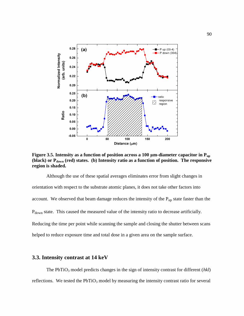
90
Figure 3.5. Intensity as a function of position across a 100 μm-diameter capacitor in Pup
(black) or Pdown (red) states. (b) Intensity ratio as a function of position. The responsive
region is shaded.
Although the use of these spatial averages eliminates error from slight changes in
orientation with respect to the substrate atomic planes, it does not take other factors into
account. We observed that beam damage reduces the intensity of the Pup state faster than the
Pdown state. This caused the measured value of the intensity ratio to decrease artificially.
Reducing the time per point while scanning the sample and closing the shutter between scans
helped to reduce exposure time and total dose in a given area on the sample surface.
3.3. Intensity contrast at 14 keV
The PbTiO3 model predicts changes in the sign of intensity contrast for different (hkl)
reflections. We tested the PbTiO3 model by measuring the intensity contrast ratio for several

91
reflections at 14 keV. Line scans across the capacitor for each polarization direction were
compared to give the intensity ratio, as in Section 3.2.4. The experimental values for each
reflection in Table 3.1 are the average of two to three separate sets of line scans with the
standard deviation taken as an estimate of the error.
Reflection Experimental Ratio PbTiO3 model
(003) -0.237 ± 0.022 -0.167
(004) 0.205 ± 0.027 0.160
(104) -0.345 ± 0.017 -0.145
(105) 0.150 ± 0.024 0.117
Table 3.1. Comparison between predicted and experimental values of the intensity
contrast ratio at 14 keV.
The PbTiO3 scattering model predicts the correct sign for the ratio at 14 keV, but it
does not accurately predict the amplitude. This suggests that the atomic displacements after
polarization reversal can accounted for by the (-h-k-l) structure factor, but that the scattering
factors and atomic positions in the PZT solid solution need to be taken into account to
accurately predict the magnitude of intensity contrast.
3.4. Resonant enhancement of intensity contrast
We measured the energy dependence of the intensity contrast ratio for the {004}
reflections above and below the Pb Lα1 edge in order to test the energy dependence of the
PbTiO3 model. In our PbTiO3 model, the increase in f ' and f " at the absorption edges causes
a similar increase in the contrast ratio at absorption edges. At energies below the absorption

92
edge, our PbTiO3 model predicted that the ratio would be small (less than 0.05) and constant.
Above the edge, the PbTiO3 ratio model predicts a larger value of the contrast, up to 0.4 or
0.5, and that this value will gradually decrease for higher x-ray energies.
Measurements were conducted quickly to minimize beam damage to the sample. The
remnant polarization and the intensity of Bragg reflections decreased when the beam was left
in one spot for an hour or two. Hysteresis loops were taken periodically to measure Pr and
avoid taking data from damaged capacitors. For the {004} intensity ratio measurements, we
arbitrarily chose a value of the remnant polarization at which we would no longer use the
devices. When 2Pr dropped below 60 μC/cm2 for a particular capacitor, we stopped using it
and moved to a new device to continue the measurement. The ratios of the {003} and {004}
reflections were measured at energies from 12.4 keV to 14.0 keV are shown in Figure 3.6.
Figure 3.6. Intensity ratio of {003} and {004} PZT reflections versus incident x-ray
energy. The sharp increase in the {004} ratio is at the Pb L3 edge at 13.035 keV.

93
The sharp increase in the intensity ratio of the {004} reflection at the Pb L3 edge near
13.035 keV is exactly what we expected, based on the increase in f " at the absorption edge.
Small oscillations slightly above the edge may be due to the fine structure of the orbitals in
the coordinated PZT molecules, as opposed to the elemental Pb atoms considered in the
qualitative predictions of Section 3.1.2.
The large fluctuations far from the absorption edge cannot be explained in the same
way. For example, the ratio is predicted to be less than ± 0.05 for all reflections between 12.4
and 13.0 keV. There are no absorption edges in any of the other constituent elements (Zr, Ti,
and O) anywhere near these energies.
The maximum value of the {003} ratio versus energy was observed at 13.035 keV.
However, the rest of the data do not match our qualitative predictions. We know that the
error bars do not accurately represent the variation between measurements at the same energy,
so that may account for some of the deviation. The qualitative model does not account for the
sign of the positive ratio at 12.7 keV. This point was measured twice to confirm the sign of
the intensity change at this energy.
Several potential sources of error were eliminated. The mosaic block rotations were
averaged out by taking line scans. We do not believe that fatigue is a major cause for
uncertainty in the ratio measurements, since the capacitors were switched less than 1,000
times before noticing a decrease in intensity ratio at the same energy. Fatigue typically sets in
after 105-10
7 switching cycles in similar devices.
17 Artifacts from beam damage were
avoided as well. We found that the degradation in Pr occurred before the diffracted intensity
94
was affected. For example, over the course of three ratio measurements, Pr decreased from
0.93 μC/cm2 to 0.77 μC/cm
2 while ratio measurements remained the same.
3.5. Refinement of the kinematic scattering model
Structure factor calculations using a PbTiO3 unit cell do not account for some features
in the experimental measurements of the intensity contrast ratio. Several models were tested
to determine why the observed intensity ratio is larger than the predicted one. In each model,
the structure factor for the (hkl) and (-h-k-l) reflections is derived and the intensity ratio is
calculated.
We carefully selected values of the atomic scattering factors to be sure that they were
as accurate as possible. Values of f0 were taken from a parameterization derived by
Waasmaier and Kirfel.20
The Waasmaier-Kirfel ionic scattering factors are available for a
wide variety of ions for values of q = 0-6 Å-1
, where q is in units of sin(θ)/ . Calculated
values of f0(q) were exported from the DABAX function in XOP 2.18 in 0.02 Å
-1 steps for
Pb2+
, Zr4+
, Ti4+
, and O2-
. They were then imported into Mathematica and linearly
interpolated for use in the structure factor calculations.
We used the most accurate values available for the dispersion corrections. Values of f
' and f " were taken from tabulations in Henke et al.11
which are the default values in XOP.
They are for the elemental, not the ionized form of the atoms. There are data points 0.1 eV
above and below the absorption edge and 500 more data points on a logarithmic scale from 10
to 30,000 eV. Note that XOP outputs f1 in units of f ' + f0 (q = 0).
95
3.5.1. Model 1: a perfectly disordered alloy
The PbTiO3 model is not accurate enough to describe the scattering from the PZT thin
film. An important difference between the PbTiO3 model and the PZT thin films used in the
experiment is that the Ti central atom of PbTiO3 is replaced by either a Ti or Zr atom.
Pb(Zr,Ti)O3 is a substitutional alloy, so we assumed that PZT is a perfectly disordered alloy
and that there is no correlation in the identity of central atoms in neighboring unit cells. The
chance of a Zr atom occupying the site is equal to atomic fraction of Zr atoms, 45%; for Ti,
55%.
The structure factors for a PZT random alloy were calculated. In a perfectly
disordered alloy, the atomic scattering factor of the central atom can be replaced by the
occupancy-weighted average of the scattering factors of the two alloy atoms.8 With
compositions of Zr and Ti given by cZr and cTi, respectively, the average scattering factor for
the central atom is thus:
Inserting the faverage into a single unit cell of PZT and gives the following expression for
structure factor:
( )
Atomic positions rPb, rO1, rO2, rO3, and rZr/Ti were taken from the Reitveld refinement of
neutron powder diffraction data from a tetragonal Pb(Zr.48, Ti.52)O3 sample in a study
conducted by Noheda et al.21
The intensity ratio was calculated using the same expression as

96
in Section 3.1.2. The ratio for the {003} and {004} reflections as a function of energy is
shown below Figure 3.7
Figure 3.7. Ratio predicted by perfectly disordered alloy model compared with
experimental data.
The random alloy model predicts the sign and magnitude better than the PbTiO3
model. Better estimates of f " were the most significant improvement. However, this model
does not explain the positive {003} ratio at 12.7 keV or the large ratios of the {004} below
the Pb edge.
3.5.2. Model 2: supercell approximation of a random alloy
Structural refinements of neutron diffraction from PZT powders indicate that Zr and Ti
have slightly different positions within the unit cell.22
The Ti4+
ions shift further from the
97
centrosymmetric position as a function of composition – the closer to the morphotropic phase
boundary, the larger the displacement from the center of the unit cell. They list the atomic
positions for several compositions of PZT, and chose to use the positions for the
PbZr0.4Ti0.6O3 composition.
To model the difference in atomic positions between two atoms, it was no longer
possible to use only one unit cell for the structure factor calculations. A supercell consisting
of 100 perovskite unit cells was generated to calculate the structure factor. The central atom
in each unit cell was randomly chosen such that there was a total of 45 Zr4+
and 55 Ti4+
ions
in the entire supercell. The matching ionic scattering factor (either fZr or fTi) was used for the
central atom of each unit cell. f0 was taken from the DABAX tabulations of calculated values
from Waasmaier and Kirfel20
and the dispersion corrections were taken from DABAX
tabulations of calculations in Henke et al.11
The ratio from this Zr/Ti position difference model is not significantly different from
the results of the disordered alloy model. Both models share the same trends – low values for
the ratio between 10 – 13 keV, a sharp increase at the Pb Lα1 absorption edge, and large
values which decrease slowly at higher energies. The maximum difference between the two
calculated values was at the absorption edge; 0.04 for the {003} and 0.03 for the {004}.
Average values for Zr/Ti difference model were 0.02 higher than those calculated by the
disordered alloy model. This is around a 1-2% difference between the two models. We
conclude that the difference in the Zr and Ti atom‟s positions within the unit cell is not a
significant source of intensity contrast between the two polarization directions. .

98
3.5.3. Potential future refinements of these models
The models proposed so far provide a reasonable fit for energies at and above the
absorption edge. However, neither model can explain the large contrast ratio at energies far
from the absorption edge.
One possibility is that the atomic positions of this thin film sample could be drastically
different than those in the powder samples used in the structure determination studies cited
above. This theory was tested by varying the atomic positions and calculating the contrast
ratio. The (002) reflection was selected because the intensity contrast of (00l) reflections
depends only on f " and the fractional coordinate w for each atom. I calculated the contrast
ratio of the {002} reflection at 10 keV as a function of w for the central atom. This was
repeated for the Pb atom as well. Moving the Pb or the Ti/Zr atom along the z axis produces
a maximum contrast ratio of 0.15 for the {002} reflections at 10 keV, compared to the
experimental value of 0.2 – 0.3. It should be noted that this value for the ratio occurs when
the Pb atom is moved 0.726 Å below the basal plane of the unit cell (away from the central
atom). A displacement this large seems to be impossible, so we believe that the ratio at low
energies is not caused by a change in atomic positions in thin films.
Another possibility is that the dispersion corrections are different for these ions than for
non-ionized atoms. It is known that ionization changes the dispersion corrections near
absorption edges, but there may be some modifications far from the edge as well. Or there

99
may be some systematic experimental factor that is more prevalent at lower energies that was
not accounted for.
The biggest improvement to the kinematic scattering model was adding the correct
atomic scattering factors. The perfectly disordered alloy model with dispersion corrections
for Pb2+
, Zr4+
, Ti4+
, and O2-
accurately predicted the intensity ratio near the Pb L3 edge. The
differences in atomic positions in PbTiO3 and PZT played a more subtle role. We learned
that the differences between the PZT structural refinement in Noheda et al. and that in Frantti
et al. did not have a large effect on the intensity ratio.5,22
In fact, even impractically large
displacements of Pb and Zr/Ti ions were not sufficient to explain the observed ratios of the
{002} or {004} at energies below the Pb edge.
3.6. Conclusion
In ferroelectric materials, the intensity of a Bragg reflection depends on the
polarization direction. The atomic displacement associated with the polarization changes the
structure factor. The change in intensity upon switching the polarization was calculated by
computing the structure factor for the (hkl) and (-h-k-l) reflections. The intensity contrast
induced by polarization switching was measured experimentally using x-ray microdiffraction
for several reflections as a function of energy. Predicted values were compared to the
experimental measurements in order to refine the kinematic scattering model.
The precise atomic positions within the PZT unit cell were less important in predicting
the intensity contrast accurately than using the correct atomic scattering factors. The biggest

100
improvement from the PbTiO3 model was achieved by approximating the scattering factor of
the central Zr/Ti atom as a compositionally weighted average of the Zr and Ti scattering
factors. This approach was most accurate near absorption edges, where the imaginary
component of the dispersion correction is largest and the change in intensity is most
noticeable. However, at energies far from an absorption edge other sources of contrast
become more prevalent in PZT. Artificially displacing the Pb and Zr/Ti atoms could not
account for the large intensity contrast at energies well below the Pb L3 edge. We suggest
that the dispersion corrections of the cations in PZT are different than those tabulated in
Waasmaier and Kirfel.20
101
3.7. Chapter 3 references
1 J.Y. Jo, P. Chen, R.J. Sichel, S.-H. Baek, R.T. Smith, N. Balke, S.V. Kalinin, M.V. Holt, J.
Maser, K. Evans-Lutterodt, C.-B. Eom, and P.G. Evans, “Structural Consequences of
Ferroelectric Nanolithography,” Nano Lett., Article ASAP, (2011). doi: 10.1021/nl2009873
2 S. J. van Reeuwijk, K. Karakaya, H. Graafsma and S. Harkema, “Polarization switching in
BaTiO3 thin films measured by X-ray diffraction exploiting anomalous dispersion” J. Appl.
Cryst. 37, 193 (2004).
3 D.-H. Do, “Investigation Of Ferroelectricity And Piezoelectricity In Ferroelectric Thin Film
Capacitors Using Synchrotron X-Ray Microdiffraction,” PhD thesis, University of Wisconsin-
Madison (2006).
4 D.-H. Do, P. G. Evans, E. D. Isaacs, D. M. Kim, C.-B. Eom and E. M. Dufresne, "Structural
visualization of polarization fatigue in epitaxial ferroelectric oxide devices," Nature Mater. 3,
365 (2004).
5 B. Noheda, D. E. Cox, G. Shirane, J. A. Gonzalo, L. E. Cross, and S. E. Park, “A monoclinic
ferroelectric phase in the Pb(Zr1−xTix)O3 solid solution,” Appl. Phys. Lett. 74, 2059 (1999).
6 R. D. Shannon, “Revised effective ionic radii and systematic studies of interatomic distances
in halides and chalcogenides”, Acta Cryst. A 32, 751 (1976).
7 S. Nishikawa and K. Matsukawa, “Hemihedry of Zincblende and X-ray Reflexion,” Proc.
Imp. Acad. Japan, 4, 96 (1928).
8 M. Sanchez del Rio and R. J. Dejus, "Status of XOP: an x-ray optics software toolkit" SPIE
Proceedings 3448, 340 (1998).
9 R. W. G. Wyckoff, Crystal Structures. Vol. 2, p. 401, (John Wiley & Sons, New York,
1963).
10 J. Als-Nielsen and D. McMorrow, Elements of Modern X-ray Physics, (John Wiley & Sons,
West Sussex, England, 2001).
11 B.L. Henke, E.M. Gullikson, and J.C. Davis, “X-ray interactions: photoabsorption,
scattering, transmission, and reflection at E=50-30000 eV, Z=1-92,” Atomic Data and
Nuclear Data Tables 54, 181 (1993).
12 B. Jaffe, W. R. Cook, and H. Jaffe, Piezoelectric Ceramics, (Academic Press, London and
New York, 1971).

102
13
C. B. Eom, R. B. Van Dover, J. M. Phillips, D. J. Werder, J. H. Marshall, C. H. Chen, R. J.
Cava, and R. M. Fleming, and D. K. Fork, “Fabrication and properties of epitaxial
ferroelectric heterostructures with (SrRuO3) isotropic metallic oxide electrodes,” Appl. Phys.
Lett. 63, 2570 (1993).
14 J. M. Ablett, L. Berman, C. Kao, G. Rakowsky, D. Lynch. “Small-Gap Insertion-Device
Development at the National Synchrotron Light Source - Performance of the New X13
Mini-Gap Undulator,” J. Synch. Radiation 11, 129 (2004).
15 J. M. Ablett, C. C. Kao and A. Lunt, “The design and performance of an x-ray micro-
focusing system using differentially deposited elliptical mirrors at the National Synchrotron
Light Source,” Review of Scientific Instruments 73, 3464 (2002).
16 J. A. Bearden, “X-Ray Wavelengths”, Rev. Mod. Phys. 39, 78 (1967). Information from the
X-ray Data Booklet can be found online at http://xdb.lbl.gov/ .
17 K. Rabe, C. H. Ahn, J.-M. Triscone (Eds.), Physics of Ferroelectrics, (Springer-Verlag,
Berlin, Germany, 2007).
18C. M. Foster, G.-R. Bai, R. Csencsits, J. Vetrone, R. Jammy, L. A. Wills, E. Carr, and J.
Amano,“Single-crystal Pb(ZrxTi1−x)O3 thin films prepared by metal-organic chemical vapor
deposition: Systematic compositional variation of electronic and optical properties,” J. Appl.
Phys. 81, 2349 (1997).
19
T. J. Zhua, L. Lub, X. B. Zhao, Z. G. Jia, J. Mac, “Epitaxial growth and ferroelectric
properties of Pb(Zr0.52Ti0.48)O3/SrRuO3 heterostructures on exact SrTiO3 (001) substrates,”
J. Cryst. Growth 291, 385 (2006).
20 Waasmaier and Kirfel, “New Analytical Scattering-Factor Functions for Free Atoms and
Ions,”Acta. Cryst. A 51, 416 (1995).
21 B. Noheda, J. A. Gonzalo, L. E. Cross, S. E. Park, D. E. Cox, and G. Shirane, “Tetragonal-
to-monoclinic phase transition in a ferroelectric perovskite: The structure of PbZr0.52Ti0.48O3”
Phys. Rev. B 61, 8687 (2000).
22 J. Frantti, S. Ivanov, S. Eriksson, H. Rundlof, V. Lantto, J. Lappalainen, and M. Kakihana,
“Neutron diffraction and bond-valence calculation studies of Pb(ZrxTi1-x)O3 ceramics,” Phys. Rev.
B 66, 064108 (2002).

103
Chapter 4. Piezoelectric Response of BiFeO3 (001) Thin Films
4.1. Introduction
All ferroelectric materials are piezoelectric, including BiFeO3. Piezoelectric materials
change size and shape when an electric field is applied. Conversely, when a piezoelectric
material is compressed or stretched it develops a polarization proportional to the stress. Since
materials may expand in one direction and contract in another, the piezoelectric coefficients
are described using tensor notation. The piezoelectric response of BiFeO3 is important for
both electromechanical applications and for the potential control of its magnetism using
electric fields.
There are several reasons why BiFeO3 has attracted so much attention in recent years.
For one, the piezoelectric properties of BiFeO3 could be used in electromechanical actuators
and transducers. Also, physicists have taken an interest in BiFeO3 thin films because they
provide an attractive system for examining several effects of electromechanical coupling.
Evidence for strain-driven morphotropic phase transformations have been found in highly
strained films of BiFeO3.1, 2
Studies of BiFeO3 and other materials have also revealed subtle
ferroelectric effects such as bond lengthening under electric field and rotations of the
material‟s polarization vector. 3,4
Additionally, epitaxial strain has been shown to change the
piezoelectric response and ferroelectric polarization.5
In addition to its usefulness in the development of materials for purely mechanical
applications, determining the piezoelectric response of BiFeO3 is crucial to its eventual use in

104
magnetoelectric devices. When the ferroelectric polarization state and antiferromagnetic
ordering are dependent on one another in a material, the link between order parameters is
known as multiferroic coupling.6 It is important to understand the multiferroic coupling in
BiFeO3 because the Fe-O-Fe bonds which modify magnetic ordering are affected by changes
in the lattice constants.7 The electromechanical coupling is of particular interest for BiFeO3
because it is related to the multiferroic properties. Magnetic ordering in transition metal
perovskites is mediated by the superexchange interaction between transition metal ions via a
polarization of the atomic orbitals of the oxygen ions.8 In BiFeO3, calculations using density
functional theory suggest that the magnetic interaction is sensitive to the tilt and rotation of
the FeO6 oxygen octahedra.9 When BiFeO3 is subjected to an electric field, piezoelectric
strain can modify the magnetic ordering by distorting the oxygen octahedra. The details of
the structural changes induced by applied electric fields must be studied before we can fully
understand and manipulate the magnetism.
Time-resolved synchrotron x-ray microdiffraction was used to determine the
piezoelectric coefficients by measuring the strain developed when an electric field is applied
to the sample. These thin films have multiple structural variants with differing
crystallographic orientations (see Chapter 2). Since the piezoelectric response is largest along
the pseudocubic [111] direction, the structural variants could each have different strains under
the same electric field. We find that the strain along the out-of-plane direction is the same for
all variants. The in-plane piezoelectric coefficients vary unpredictably and are not correlated
with the crystallographic orientation of BiFeO3.

105
4.1.1. Piezoelectric tensor
Piezoelectricity results in two important effects. In the direct piezoelectric effect, a
stress applied to the material results in an internal electric field. The resulting voltage can be
measured and used to determine the electric field. The direct piezoelectric coefficient e is the
constant of proportionality between the magnitude of the strain generated in the material by
the applied stress and the electric field. In the converse piezoelectric effect, an applied
electric field results in strain. The converse piezoelectric coefficient d relates the applied
electric field and the strain. These experiments focused on the converse piezoelectric effect
in order to determine the effects of electric field on the structure and bond angles.
In the limit in which the piezoelectric strain is exactly proportional applied electric field,
the strain tensor and electric field are related by εjk = dijk · Ei, where ε is the strain, d is the
piezoelectric coefficient, and E is the applied electric field.10
Piezoelectricity is a tensor
property so that applying an electric field along one direction can produce strains and shears
along orthogonal directions as well. The units of the converse piezoelectric coefficient are
distance divided by potential difference. Values of the piezoelectric coefficient are often
given in pm/V. The three-index notation in the equation above can be condensed to a two-
index notation, dij. The first index i refers to the electric field direction in the conventional
manner where 1,2, and 3 refer to the x, y, and z directions, respectively. The second index j
refers to elements in the strain tensor using Voigt notation.10
The tensor of converse
piezoelectric coefficients dij relates the piezoelectric strain εj to the electric field Ei :

106
[
] [
] [
].
We use the pseudocubic notation for the BiFeO3 piezoelectric tensor and x-ray
reflections in order to emphasize the epitaxial relationship between film and substrate. The
rhombohedral symmetry of BiFeO3 is not apparent from this notation, which has the side
effect of complicating the expression for the piezoelectric tensor. When the piezoelectric
tensor is projected onto a basis parallel to high symmetry directions such as the [100], [010],
and [001] directions of a tetragonal material, most of the terms are equal to zero while many
of the remaining coefficients are identical.10
However, simplifications that can be made to
the piezoelectric tensor dij based on symmetry relationships a tetragonal system are not
possible in BiFeO3 thin films, for two reasons. First the axes of the rhombohedral coordinate
system are not parallel to the pseudocubic axes used to define the piezoelectric tensor
coordinate system. More importantly, the film is under anisotropic epitaxial strain, reducing
the symmetry in the plane of the film. In this chapter we use the pseudocubic notation and
the pseudocubic coordinate system to define strain, electric field direction, and the
piezoelectric coefficient tensor and we make no symmetry-based simplifications to the
piezoelectric tensor.
A second definition of the piezoelectric coefficients is widely used in conjunction with
polycrystalline piezoelectric ceramics. The notation and units are identical to the ones
described above, often leading to confusion. In this so-called engineering notation, the
piezoelectric coefficients are defined so that the z direction corresponding to subscript 3, is

107
defined to be in the direction of the applied electric field. The expansion along the field
direction is thus determined by the piezoelectric coefficient d33 in the engineering notation.
The symmetry of the piezoelectric tensor is also different between the two definitions. In the
crystallographic definition the piezoelectric tensor has the symmetry of the crystallographic
unit cell. In the engineering definition, the tensor has the same symmetry as the overall shape
of the piezoelectric solid, which can be quite different from the crystallographic symmetry.
We chose a coordinate system with z parallel to the out-of-plane direction. We chose
this system in order to make z parallel to the electric field applied across the electrodes above
and beneath the film. For (001)-oriented thin films the electric field nearly parallel to the
pseudocubic c axis of the film. In this case E1 and E2 are zero and only E3 is non-zero. The
piezoelectric coefficients which determine the tensile or compressive strain are d31, d32, and
d33, and changes in shape of the unit cell (shear strains) are determined by d34, d35, and d36.
Measuring piezoelectric strain in thin films can be difficult. In bulk materials the
piezoelectricity can be measured using interferometry, in resonators, or by observing the
mechanical distortion using a profilometer. In thin films, piezoelectricity must be observed
using a different set of techniques. In wafer-bending measurements of piezoelectricity, the
change in the electrical polarization of the film is measured when the substrate is bent using a
pressure cell, providing the direct piezoelectric coefficient.11
The drawback of the wafer-
bending approach is that it requires knowledge of precise values of the Young‟s modulus and
the Poisson ratios to give accurate results. These values are note always available, especially
for new materials. Another approach is to use focused ion beam milling or selective etching
to create a bridge structure or cantilever into the film by removing a section of the underlying

108
substrate.12
A DC voltage is applied and the deflection of the bridge or elongation of the
cantilever is measured optically, enabling the experimenter to calculate d31. Potential
problems with this method are that the film can be damaged during the substrate removal
process and that DC electric fields must be applied, so the field magnitude must be kept small
to avoid dielectric breakdown.
Time-resolved microdiffraction probes both the out of plane and the in-plane
piezoelectric response while avoiding the difficulties of other techniques. The strains ε1, ε2,
and ε3, can be determined from changes in the pseudocubic a, b, and c lattice constants,
respectively. The experiments in this chapter measure piezoelectric strain in BiFeO3 thin
films by detecting changes in the lattice constants while an electric field is applied. We find
that d33 is constant for the entire film, but the in-plane piezoelectric response varies from
place to place in the sample.
4.2. Experimental methods
4.2.1. Experimental setup
The sample used for these measurements was the same as for the experiments
described in Chapter 2. The layer structure consisted of a 400 nm BiFeO3 thin film on a
SrRuO3 thin film bottom electrode grown on a (001) SrTiO3 substrate miscut by 3.1° along
the [010] direction. The sample had Pt top electrodes of varying diameters grown by sputter
deposition through a shadow mask on top of the BiFeO3 surface. The top electrodes defined

109
capacitor structures, which allowed an electric field to be applied across the thickness of the
film.
The x-ray diffraction experiments were conducted at the Advanced Photon Source.
X-rays at photon energies of either 11.5 or 10 keV were selected by a Si (111) double-crystal
monochromator. The incident x-ray beam was focused using a Fresnel zone plate as described
in Section 1.7.3.2. The diffraction volume probes only material that is subjected to the
electric field and does not include any signal from the regions outside the electrodes. The
experiments were done in two segments. Measurements of the piezoelectricity along the out-
of-plane direction in high electric fields were done at Sector 7-ID-C using the nanosecond-
scale time resolved technique explained in Section 1.7.4.2. For these high-field piezoelectric
measurements, the incident beam had a photon energy of 10 keV, a spot size of 130 nm at full
width half maximum, and the sample-to-detector distance was 285 mm. Measurements of the
in-plane piezoelectricity were conducted at Sector 2-ID-D using the millisecond-scale time
resolved technique in Section 1.7.4.1 with a photon energy of 11.5 keV, x-ray spot size of 275
nm, and sample to detector distance of 310 mm. Both experiments used an APD to detect
scattered x-rays. The detector angular resolution was determined by the size of slits placed
directly in front of the detector.
The experimental procedure was similar for both measurements. In both cases, we
first found the Bragg reflections for each component of the sample near the SrTiO3 (002)
reflection to determine the out-of-plane lattice constant of the BiFeO3. To do this, the sample
and detector were rotated to the angles predicted for the (002) Bragg reflections. The incident
angle, , diffracted angle, 2θ, and sample tilt angle, χ, were varied to find the maximum of the

110
BiFeO3 (002) reflection. These angles are shown schematically in Figure 1.7. A -2θ scan
through the series of reflections near the SrTiO3 (002) reflections is shown in Figure 4.1. The
SrTiO3 (002) reflection was used to calibrate the observed values of θ and 2θ, based on its
reported bulk lattice constant of 3.905 Å.
Figure 4.1. θ-2θ scan of the SrRuO3 (220), BiFeO3 (002), and SrTiO3 (002) reflections
with a photon energy of 10 keV.
The lattice constants of the films were determined using the angular positions of the
Bragg reflections in Figure 4.1. From these measurements we found that BiFeO3 had a lattice
constant cBFO = 4.01 Å. This is slightly larger than the bulk pseudocubic lattice constant of
BiFeO3, 3.96 Å.13
The SrRuO3 has a pseudocubic lattice constant cSRO = 3.96 Å. The width
of the BiFeO3 peak is caused by the range of strain states and orientations within the film due
to partial relaxation described in Chapter 2.

111
4.2.2. Time resolved x-ray diffraction
The piezoelectric strain was measured by simultaneously applying an electric field
and measuring the time resolved x-ray diffraction. An electrical probe tip contacted the top
electrode of a capacitor structure. During the x-ray experiments we acquired a polarization-
electric field hysteresis loop to be sure that the particular device was switchable and that it
had a remnant polarization similar to the expected value. Maps of diffracted intensity over
the sample surface were used to place the focused beam and probe tip on the same capacitor.
A similar procedure for bringing the beam and the tip to the same position is described in
Section 3.2. In order to minimize structural artifacts arising from beam damage the sample
was occasionally moved in steps of several microns to bring the x-ray spot to a region of the
BiFeO3 film that had not yet been exposed to the beam.
The time-resolved diffraction pattern was recorded while an electric field was applied
to the film. The electric field was applied while the diffracted intensity as a function of time
was recorded at each point in a scan across a Bragg reflection. During the high-electric-field
scans, the sample and detector were rotated to the first point in the scan. The voltage on the
probe tip was provided by a fast-risetime pulse generator (Picosecond Pulse Generator
2600C). Square-wave pulses with a duration of 25 ns width and voltage amplitudes ranging
between +45 V and -45 V were applied to the sample. Prior to time-resolved diffraction
measurements, we applied several 25 ns pulses with amplitudes above the coercive field.
These pulses switched the polarization direction parallel to the applied field. A series of
5,000 pulses were applied at a repetition rate of 3 kHz. The x-ray photons scattered during
the pulses were selected from the stream of x-ray photons arriving at times outside the pulses,

112
as in Section 1.7.4.2. The intensity of the x-ray reflection was determined by summing the
number of diffracted photons using one channel of a scaler (Joerger, Inc.). The intensity
measurement was repeated in steps of 0.8 ns, starting 5 ns before the rising edge of the
voltage pulse and ending 40 ns later. The entire process was then repeated for each angle of a
-2 scan. The intensities acquired in this way were then plotted to show the evolution of the
intensity near the BiFeO3 (002) Bragg reflection as a function of time.
Figure 4.2. Time resolved θ-2θ scan of the BiFeO3 (002) reflection during a 25 ns voltage
pulse. The x-ray photon energy was 10 keV.
Figure 4.2 is the intensity versus time at the (002) BiFeO3 Bragg reflection during a
voltage pulse corresponding to E=1.04 MV/cm. The field applied to the capacitor is shown in
the upper panel of the figure. The lower panel shows the diffracted intensity as a function of
time. The vertical axis is the detector angle (2θ) in a θ-2θ scan. The horizontal axis indicates
time, where 0 on the time axis corresponds to the beginning of the rising edge of the voltage

113
pulse. Each vertical line is a θ-2θ scan at one point in time. The center of the (002) reflection
shifts to a lower angle once the field is applied.
The structural signature of the capacitor charging time can be seen at the beginning
and end of the voltage pulse. The structural transient apparent just after the beginning of the
voltage pulse in Figure 4.2 has an RC time constant of 3.1 ns. The rise time of the pulse
generator is far shorter than this, approximately 300 ps. We suspect that the rise time of the
Bragg reflection is caused by the time required to charge the capacitor and that the rise time
thus depends on the time constant for charging the device rather than on a fundamental
physical time scale. We measured the piezoelectric strain using the angular position of the
(002) reflection several RC time constants after the beginning of the electrical pulse.
4.3. Measurement of out-of-plane piezoelectric coefficient d33
The piezoelectric coefficient in the out-of-plane direction was measured from the shift
in angle of the BiFeO3 (002) reflection. The strain induced by an electric field along the out-
of-plane direction is defined as ε3 in our notation. Using the Bragg equation for interplanar
spacing we find that the strain is given by:
Here the subscript 0 indicates the initial condition without electric field. Fitting a Gaussian
function to the zero-electric-field BiFeO3 (002) reflections in Figure 4.2 gives θ0 = 35.978°.
The field-induced shift of the (002) was measured for many strengths of electric field.
The (002) reflections for several electric fields are shown above in Figure 4.3. The 1.04

114
MV/cm θ-2θ scan was taken from the data in Figure 4.2. The 478 kV/cm line was taken from
θ-2θ scans during the middle of similar voltage pulses with half the amplitude, 15 ns after the
beginning of the pulse. We chose to measure at a single point in time instead of scanning in
order to reduce the total number of pulses applied to the device. The zero-field line was taken
during an identical scan without electric field as a baseline for comparison.
35.8 35.9 36.0 36.1 36.2 36.3 36.4 36.5
0
100
200
300
400
500
0 kV/cm
478 kV/cm
1040 kV/cm
co
un
ts
2 (deg.)
Figure 4.3. θ-2θ scans across the BiFeO3 (002) reflection at several electric fields.
The field we applied during the data acquisition of Figures 4.2 and 4.3 was directed
along the z direction only, so that ε3= d33E3. The piezoelectric coefficient d33 was calculated
from a least-squares fit of a line to the strain as a function of electric field, shown below in
Figure 4.4. No hysteresis is observed in the piezoelectric strain because the polarization of

115
the film was switched to be parallel to the applied field before the piezoelectric strain was
measured.
Figure 4.4. Strain ε3 versus applied electric field for positive and negative polarity fields.
The piezoelectric coefficient is determined from the slopes of the linear fits to the strain
versus E in Figure 4.4. The piezoelectric strain is proportional to the applied field for both
signs of the applied electric field, as expected at these magnitudes of electric field.14
The
value of d33 determined from Figure 4.4 is 53 pm/V. This coefficient is similar to values
found by piezoresponse force microscopy (PFM), which range from 50 to 60 pm/V.15
Agreement between PFM and x-ray diffraction measurements of d33 indicate that the
film is strained homogenously. This is because PFM experiments measure the displacement
of the film underneath a conductive tip, whereas diffraction measures the average lattice
constant. The width of an x-ray reflection in θ-2θ is a measure of the variation in interplanar
spacing within the diffraction volume. An increase in the width of the reflection would
116
indicate that the film was not strained homogeneously. The peak width of the (002) reflection
is constant with E below 1 MV/cm. This means that the entire film has the same
piezoelectric strain rather than having regions with different piezoelectric coefficients with an
average value of 53 pm/V.
4.4. In-plane piezoelectric response and d31
The piezoelectric tensor includes components that lead to distortions of the crystal in
directions that are orthogonal to the applied field. In thin films, elastic constraints due to the
substrate and to the shape of the thin film make the piezoelectric distortion in this direction
difficult to predict. We predict that a piezoelectric strain in the in-plane direction, i.e. in the
plane of the surface, will only be possible if the film is not coherent and epitaxial. In an
epitaxial film with no defects, the film is clamped by the substrate and the film is prevented
from expanding or contracting along the in-plane direction.16
Clamping effects force the
effective d31 to be zero in thin films that cannot change their lateral dimensions or relax
elastically in some other way.17
We measured the in-plane piezoelectric response using changes in the (103) BiFeO3
reflection while the sample was subjected to an electric field. First, a reciprocal space map of
the (103) BiFeO3 reflections was acquired without an electric field in order to identify the
structural variants present in the film. The structural variants are signatures of polarization
domains, as described in Chapter 2. Then reciprocal space maps are taken as a function of
time while electric field is applied. The change in angle of each reflection is used to calculate

117
the strain for each structural variant. Finally, the linear dependence of strain on electric field
was measured to obtain the piezoelectric coefficients for each structural variant.
4.4.1. Multiple (103) reflections of structural variants
The zero-field BiFeO3 (103) reflections were measured to identify the structural
variants present in the film and to determine the strain state before applying electric field.
The in-plane strain can be measured using an x-ray reflection with a wavevector that has a
component in the plane of the surface of the sample. For a pseudocubic thin film grown with
a (001) orientation this would correspond to any reflection in which the Miller index h or k is
not zero. The change in interplanar spacing due to piezoelectricity can be found by applying
the Bragg equation to the magnitude of the wavevector of the reflection. Decomposing the
distortion into in- and out-of-plane components of strain is more difficult. .
We chose the (103) x-ray reflection for studies of the in-plane piezoelectricity for
several reasons. First, the (103) reflection is geometrically accessible using x-rays at the
photon energies that we could focus onto the sample using the Fresnel zone plate. Second,
the x-rays incident on the sample in studies of the (103) reflection have a large incident angle
of 43.8° at 11.5 keV. This allows us to have a small footprint of the focused beam on the
sample, which is useful in studying the piezoelectricity of individual grains or mosaic blocks.
A structural study of the BiFeO3 thin film reveals that it is not completely
pseudomorphic. The distribution of intensity in reciprocal space near the (103) x-ray
reflection of BiFeO3 is shown in Figure 4.5, in which reflections from BiFeO3 and SrRuO3
appear. The presence of multiple reflections from BiFeO3 indicates that more than one
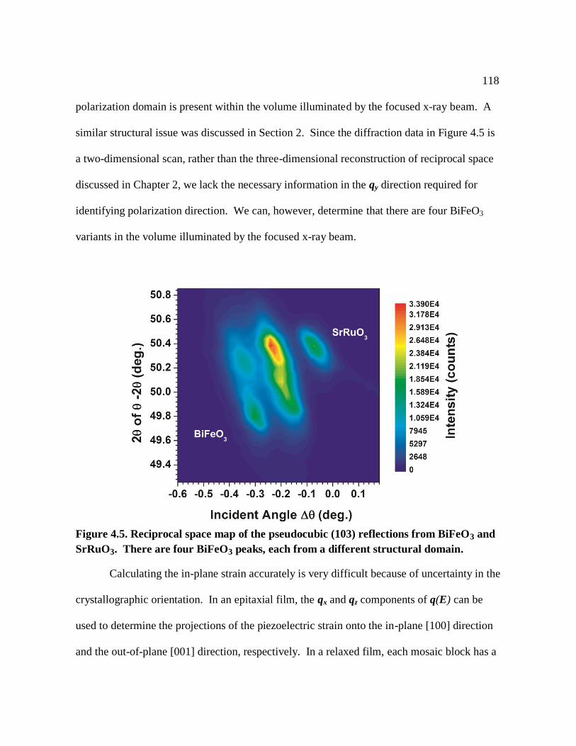
118
polarization domain is present within the volume illuminated by the focused x-ray beam. A
similar structural issue was discussed in Section 2. Since the diffraction data in Figure 4.5 is
a two-dimensional scan, rather than the three-dimensional reconstruction of reciprocal space
discussed in Chapter 2, we lack the necessary information in the qy direction required for
identifying polarization direction. We can, however, determine that there are four BiFeO3
variants in the volume illuminated by the focused x-ray beam.
Figure 4.5. Reciprocal space map of the pseudocubic (103) reflections from BiFeO3 and
SrRuO3. There are four BiFeO3 peaks, each from a different structural domain.
Calculating the in-plane strain accurately is very difficult because of uncertainty in the
crystallographic orientation. In an epitaxial film, the qx and qz components of q(E) can be
used to determine the projections of the piezoelectric strain onto the in-plane [100] direction
and the out-of-plane [001] direction, respectively. In a relaxed film, each mosaic block has a

119
slightly different orientation with respect to the substrate, and the (103) reflection will be
rotated about in reciprocal space. The coordinate axes, and therefore the projections of q onto
qx and qz are different for each mosaic block. The mosaic block structure of the BiFeO3 is
such that the orientation of the individual blocks varies randomly on the 1 μm scale. Changes
in qx can thus in principle arise from either changes in the lattice constant or in the orientation
of the blocks.
One solution to this problem is to measure more than one reflection from the same
domain. By measuring multiple reflections we would be able to determine both the
orientation of the mosaic block and its lattice constants. This is not feasible because it
requires rotating the sample in order to reach the Bragg condition of the next reflection.
After rotating to a different incident angle, the focused beam hits a different spot on the
sample because the sample and focused beam are not exactly in the center of rotation of the
goniometer. Previous attempts to re-find the same spot on the sample after rotating between
the (002) and (103) reflections were not successful, even when we used landmarks visible to
the diffracted intensity maps, such as the edge of an electrode. The best registry between
(002) and (103) intensity maps we achieved was on the order of several microns, which is
insufficient considering the mosaic block size of 1 μm.
4.4.2. Variations of the in-plane piezoelectricity
We observe that the in-plane piezoelectric response is not zero as expected for an
epitaxial thin film. For a perfectly clamped film in which the in-plane lattice constants are
fixed to that of the substrate, there can be no piezoelectric contraction along the in-plane
direction. We thus expect d31 to be zero for a clamped film. In the opposite, bulk-like case,
120
in which there is no mechanical constraint imposed by the substrate we expect d31 to be non-
zero, as in bulk ceramics.18
We know that the 400 nm BiFeO3 film is partially relaxed, so we
expect d31 to be non-zero as in polycrystalline piezoelectric materials.
A reciprocal space map of several BiFeO3 pseudocubic {103} reflections was
measured as a function of time to determine the piezoelectric strain in each structural variant.
The time dependent diffraction pattern was obtained using the millisecond-scale method
described in Chapter 1.7.4.1. The result was a series of reciprocal space maps, each taken
with a different electric field. Within one reciprocal space map, the four BiFeO3 reflections
were fit to Gaussian functions to determine the angle at the center of the peak. These angles
were used to calculate the positions in reciprocal space of the BiFeO3 reflections. This
process was repeated for each reciprocal space map to get the peak positions as a function of
electric field.
The piezoelectric response was visualized by plotting the BiFeO3 pseudocubic {103}
positions in reciprocal space at several electric fields. Figure 4.6 shows a plot of the
reciprocal space positions of the BiFeO3 pseudocubic {103} reflections. The evolution of
these reflections in an applied electric field is shown as a trail of points in Figure 4.6. Arrows
indicate the direction of motion with increasing E, ranging from 0 to 250 kV. The distortion
evident in Figure 4.6 is a result of two closely related effects in piezoelectricity. The first is
the piezoelectric expansion of the lattice. A second more subtle effect is the rotation of the
{103} planes as the c lattice constant increases, which rotates the peak position about the
origin in reciprocal space.

121
Figure 4.6. Peak position of BiFeO3 {103} reflections under electric fields from 0 to 250
kV/cm. The SrRuO3 reflection does not move, indicating no strain in the bottom
electrode.
Apparent values of d33 and d31 for each domain are shown next to the reflections in
Figure 4.6. The piezoelectric constants were determined by calculating the change in qx and qz
at each electric field and fitting them to linear functions, where the slope of each line is taken
to be the piezoelectric coefficient. The coefficients calculated in this manner do not account
for rotations of the atomic planes and only represent apparent values. Nevertheless, it is clear
that the piezoelectric response is different for each domain. The apparent value of d31 of
domains at this position ranges from -37 pm/V to +0.69 pm/V. At another position on the
sample, a domain with an even more positive d31 = +10pm/V was found.
We interpret the non-zero d31 to mean that these domains are no longer completely
clamped. The likely explanation for the different values of d31 is that each domain is under

122
different stress states due to the incomplete relaxation of the film. A domain near the edge of
a mosaic block any other type of defects would be under very different mechanical constraints
than one in a perfectly epitaxial region of the film.
Crystal symmetry also plays a large role in the piezoelectric response. The effective
d33 measured in this experiment is not along one of the rhombohedral crystal‟s high
symmetry directions. In BiFeO3, the largest piezoelectric response is parallel to the
polarization direction along the pseudocubic [111] direction.19
When the electric field is
applied along the [001]pc direction instead, the piezoelectric tensor projected onto the new
coordinate system, and d34, d35, and d36 become large. These are responsible for shear strains
which deform the shape of the unit cell, rotating the atomic planes. Instead of variations in
d33, we believe that the variations in apparent d33 and d31 are caused by different shear strains
for each structural variant. The amount of shear strain would be affected by mechanical
constraints of neighboring domains, defects, or boundaries between mosaic blocks, resulting
in variations in the rotation of the (103) planes observed in Figure 4.6.
Shear strains are observed in other rhombohedral ferroelectric thin films. Ouyang et
al. demonstrate that for rhombohedral 0.67Pb(Mg1/3Nb2/3)O3–0.33PbTiO3 (PMN-PT) the
piezoelectric response along the pseudocubic [001] is nearly at the maximum due to
contributions from d35 and d36.20
When grown on cubic (001) SrTiO3 substrates, the film
forms multiple domains similar to BiFeO3 films on SrTiO3 substrates. Ouyang et al. suggest
the shear components of the strains from neighboring domains are locked in place by each
other as well as the substrate clamping. We hypothesize that polarization domain patterns

123
exist in which the shear strains in neighboring domains are parallel. This would allow
neighboring domains to move. The motion of the (103) would be a combination of expansion
from d33 and rotation from d35.
The in-plane piezoelectric response of the partially relaxed BiFeO3 lies between the
polycrystalline and epitaxial regimes. A completely clamped film would have an effective d31
of zero.21
Sol-gel polycrystalline Pb(Zr,Ti)O3 films show increasing d31 with increasing film
thickness, likely because of a decrease in the clamping effect of the substrate as the film gets
thicker.22
BiFeO3 domains which have non-zero d31 are likely to be in regions which are
more relaxed than regions with no in-plane piezoelectric response.
4.5. Conclusions
Relaxation of the epitaxial strain has significant consequences for the piezoelectric
response of a ferroelectric thin film. Clamping by the substrate is predicted to reduce the out-
of-plane piezoresponse.23
In this study, we found that the out-of-plane piezoelectric
coefficient d33 was 53 pm/V. It was uniform across the entire film, unlike the in-plane
response. The in-plane coefficient d31 has a wide range of non-zero values. The variation in
d31 is a consequence of epitaxial strain relaxation. The changes in magnitude and direction
are likely caused by differences in local mechanical constraints on the domain. These include
stresses from residual epitaxial strain and the local microstructure near a particular domain.

124
4.6. Chapter 4 references
1 R. J. Zeches, M. D. Rossel, J. X. Zhang, A. J. Hatt, Q. He, C. H. Yang, A. Kumar, C. H.
Wang, A. Melville, C. Adamo, G. Sheng, Y. H. Chu, J. F. Ihlefeld, R. Erni, C. Ederer, V.
Gopalan, L. Q. Chen, D. G. Schlom, N. A. Spaldin, L. W. Martin, and R. Ramesh, “A Strain
Driven Morphotropic Phase Boundary in BiFeO3,” Science 326, 977 (2009).
2 A. J. Hatt, N. A. Spaldin, C. Ederer, “Strain-induced isosymmetric phase transition in
BiFeO3”, Phys. Rev. B 81, 054109 (2010).
3 S. Tinte, K. M. Rabe, and D. Vanderbilt, “Anomalous enhancement of tetragonality in
PbTiO3 induced by negative pressure,” Phys. Rev. B 68, 144105 (2003).
4 S. Lisenkov, D. Rahmedov, and L. Bellaiche, “Electric-Field-Induced Paths in Multiferroic
BiFeO3 from Atomistic Simulations,” Phys. Rev. Lett. 103, 047204 (2009).
5 Q. Y. Qiu, R. Mahjoub, S. P Alpay, and V. Nagarajan, “Misfit strain-film thickness phase
diagrams and related electromechanical properties of epitaxial ultra-thin lead zirconate
titanate films,” Acta Mater. 58, 823 (2010).
6 H. Schmid, “Multiferroic Magnetoelectrics,” Ferroelectrics 162, 317 (1994).
7 A. M. Glazer, “Simple Ways of Determining Perovskite Structure,” Acta Cryst. A 31, 756
(1975).
8 J. B. Goodenough, “Theory of the role of covalence in the perovskite-type manganites
[La,M(II)]MnO3,” Phys. Rev. 100, 564 (1955).
9 C. E. Ederer and N. A. Spaldin, “Weak ferromagnetism and magnetoelectric coupling in
bismuth ferrite,” Phys. Rev. B 71, 060401 (2005).
10 J. F. Nye, Physical Properties of Crystals, (Oxford University Press, London, 1985).
11 J. F. Shepard, P. H. Moses, and S. Trolier-McKinstry, “The wafer flexure technique for the
determination of the transverse piezoelectric coefficient d31 of PZT thin films,” Sensors and
Actuators A 71, 133 (1998).
12 I. Kanno, S. Fujii, T. Kamada, and R. Takayama, “Piezoelectric characteristics of c-axis
oriented Pb(Zr,Ti)O3 thin films,” Appl. Phys. Lett. 70, 1378 (1997).
13 F. Kubel, H. Schmid, “Structure of a Ferroelectric and Ferroelastic Monodomain Crystal of
the Perovskite BiFeO3.” Acta Cryst B. 46, 698 (1990).

125
14
S. E. Park and T. R. Shrout, “Ultrahigh strain and piezoelectric behavior in relaxor based
ferroelectric single crystals,” J. Appl. Phys. 82, 1804 (1997).
15 S. Y. Yang, F. Zavaliche, L. Mohaddes-Ardabili, V. Vaithyanathan, D. G. Schlom, Y. J.
Lee, Y. H. Chu, M. P. Cruz, Q. Zhan, T. Zhao, and R. Ramesh, “Ferroelectric domain
structure in epitaxial BiFeO3 films ,” Appl. Phys. Lett. 87, 102903 (2005).
16 R. N. Torah, S. P. Beeby, and N. M. White, “Experimental investigation into the effect of
substrate clamping on the piezoelectric behaviour of thick-film PZT elements.” J. Phys. D:
Appl. Phys. 37, 1074 (2004)
17 V. Nagarajan, A. Roytburd, A. Stanishevsky, S. Prasertchoung, T Zhao, L. Chen, J.
Melngalis, O. Auciello, and R. Ramesh, “Dynamics of ferroelastic domains in ferroelectric
thin films,” Nature Mater. 2, 43 (2003).
18 D. Lebeugle, D. Colson, A. Forget, M. Viret, P. Bonville, J. F. Marucco, and S. Fusil,
“Room-temperature coexistence of large electric polarization and magnetic order
in BiFeO3 single crystals,” Phys. Rev. B 76, 024116 (2007).
19 Y. H. Chu, M. P. Cruz, C. H. Yang, L. W. Martin, P. L. Yang, J. X. Zhang, K. Lee, P. Yu,
L. Q. Chen, and R. Ramesh, “Domain Control in Multiferroic BiFeO3 through Substrate
Vicinality,” Adv. Mater. 19, 2662 (2007).
20 J. Ouyang, D.-M. Kim, C.-B. Eom, R. Ramesh, and A. L. Roytburd, “Orientation
dependence of the intrinsic converse longitudinal piezoelectric constant for
0.67Pb(Mg1/3Nb2/3)O3-0.33PbTiO3 ferroelectric films with a rhombohedral structure,” Smart
Materials & Structures 14, 524 (2005).
21 D.-H. Do, Investigation of ferroelectricity and piezoelectricity in ferroelectric thin film
capacitors (PhD thesis), University of Wisconsin-Madison, (2006).
22 J. F. Shepard, F. Chu, I. Kanno, and S. Trolier-McKinstry, “Characterization and aging
response of the d31 piezoelectric coefficient of lead zirconate titanate thin films,” J. Appl.
Phys. 85, 6711 (1999).
23 Q. Y. Qiu, R. Mahjoub, S. P Alpay, and V. Nagarajan, “Misfit strain-film thickness phase
diagrams and related electromechanical properties of epitaxial ultra-thin lead zirconate
titanate films,” Acta Mater. 58, 823 (2010).

126
Chapter 5. Resonant and Non-Resonant Diffraction from
Forbidden Reflections in BiFeO3
The pseudocubic representation of BiFeO3 is a powerful tool for understanding its
structure, but it is also an oversimplification that misses important details. The pseudocubic
unit cell makes it easy to visualize the displacements of Fe3+
ions, rotations of the oxygen
octahedra, and the relationship to the substrate in epitaxial thin films. Nevertheless, it does
not adequately describe the antiferromagnetic ordering, the rhombohedral symmetry, or the
glide plane parallel to the [111] direction. For these reasons, it was realized by 1969 that a
rhombohedral or hexagonal setting was necessary to describe the structural nuances of
BiFeO3.1 Recent studies of single crystals have used the point group R3c and revealed
additional modulations of the magnetic ordering.2 The epitaxial strain in BiFeO3 thin films
introduces even more complexity to the structure by modifying the lattice constants and
rotating the film.
We have observed x-ray reflections in thin films and in single crystals of BiFeO3
which are not consistent with a rhombohedral R3c symmetry. Modulations at twice the
pseudocubic interplanar spacings produce reflections that can be indexed as pseudocubic
½(hkl) planes. Initially, we believed reflections at the ½{111} could arise from magnetic
scattering, but the reflections were orders of magnitude more intense than magnetic structure
factor calculations predict. In order to determine the origin of these reflections and refine the
structure further, we measured the intensities of ½(hkl) reflections in several BiFeO3 thin
films and in a bulk sample. The photon-energy dependence of the intensity of one of these

127
reflections was measured in order to determine which ions were displaced from the published
structures. In the following sections, I describe the reflections we observed in thin film and
bulk BiFeO3, critically evaluate the possibility that the reflections arise from magnetic
scattering, and discuss other possible origins of these reflections. We have found that small
displacements of the Fe3+
ion and rotations of oxygen octahedra which are inconsistent with
R3c symmetry can result in scattering at these wavevectors.
5.1.Predicted intensities of magnetic scattering
In order to design a magnetic scattering experiment and probe the antiferromagnetic
response to an electric field, we calculated the positions and intensities of x-ray reflections
produced by the magnetic order in BiFeO3. The magnetic structure factor for ions with
delocalized magnetic orbitals is similar to the structure factor Fhkl that is used in charge
scattering calculations.3 The spin magnetic unit cell structure factor S is given by
4
∑ ⟨ ⟩
where q is the reciprocal space vector and rn is the fractional atomic position of the nth
ion.
<sn> is the spin angular momentum operator of the nth
ion and has units of Bohr magnetons.
fm(q) is the magnetic form factor which depends on the magnitude of q and is different for
each ion analogous to the atomic scattering factor. Since the orbital magnetization L for Fe3+
is nearly zero, the magnetization unit cell structure factor is assumed to be zero as well.4
Magnetic scattering also depends on the polarization of the x-rays and the spin
direction. M is the scattering amplitude which includes the polarization dependent factor

128
calculated by Blume and Gibbs.3 M is written in terms of the components of polarization of
the incident beam parallel and perpendicular to the scattering plane. These are given in the
bottom and top rows of the matrix, respectively. The prefactor ħω/mc2 is the ratio of the
photon energy to the energy equivalent of the mass of the electron photon, which is 511 keV.
This factor comes from the fundamental origin of the magnetic scattering process in the
relativistic description of Thomson scattering.5
[
]
The largest factor in the magnetic scattering amplitude for the diagonal components of M is
S·k0×k'. This factor is largest when the spin direction is perpendicular to the scattering plane.
The intensity of a reflection is proportional to the magnetic scattering amplitude times its
complex conjugate, MM*.
The relative intensities of magnetic and charge scattering was estimated. Magnetic
scattering from the G-type antiferromagnetism in BiFeO3 creates reflections at q = ½(hkl),
half the wavevector of charge scattering reflections. The magnetic scattering intensity was
estimated for a horizontal scattering geometry, the pseudocubic ½(111) planes in BiFeO3, a
horizontally polarized incident beam, and a photon energy of 7.1 keV. The magnetization of
BiFeO3 is 4.1 μB for each Fe3+
ion.6 The magnetic form factor for Fe
3+ at q = 1/d1/2(111) =
0.219 Å-1
is 0.7.7 The highest intensity occurs when the spin polarization direction is
perpendicular to the scattering plane, in which case the magnetic scattering factor is:

129
∑ ⟨ ⟩
where 2θ is twice the Bragg angle and the scattering factor is summed over the six Fe3+
ions
in the BiFeO3 unit cell. Using the atomic positions given in Kubel and Schmidt8 at 7.1 keV,
the magnetic scattering for the ½(111) reflection is:
∑
which reduces to 0.008 r02, compared to the squared structure factor for the (111) reflection of
93,969 r02. Based on these calculations, we expect magnetic reflections in BiFeO3 to be
approximately eight orders of magnitude less intense than the charge scattering reflections.
5.2. Experimental setup
We measured the intensities of ½{hkl} type reflections using x-ray diffraction in thin
films and bulk samples of BiFeO3. Four samples were used in these experiments. The
thicknesses, orientations, and layer structures of these samples are summarized in Table 5.1.
The two (001) oriented films were compared to examine the effects of thickness on the half
order reflections. A bulk crystal of BiFeO3 grown by Sang-Wook Cheong is used as a
strain-free comparison to the thin films. A 600 nm (111)-oriented BiFeO3 film was chosen as
well because this orientation avoids the cubic/rhombohedral symmetry mismatch which
complicates the film structure. The rocking curves for this sample were very small, which
caused problems described in Section 5.2.3.2, so this sample was mainly used as a reference.

130
Name Thickness /
size Substrate Orientation
Substrate
miscut
B3-2 400 nm 15 nm SrRuO3 on
SrTiO3 substrate (001)
4° towards
[010]
B-180-C 600 nm SrTiO3 (001) 4° towards
[100]
B-180-E 600 nm SrTiO3 (111) vicinal
SS-16 0.5 mm ×3 mm
×3mm n/a (001) n/a
Table 5.1. Descriptions of the samples used in experiments described in Chapter 5.
Sample B3-2 was also used in Chapter 2.
5.2.1. Synchrotron x-ray diffraction
Synchrotron x-ray diffraction experiments were conducted at Sector 2-ID-D of the
Advanced Photon Source to study the weak reflections at ½(hkl) wavevectors. A small beam
was used to eliminate broadening of the reflections from mosaic spread. The beam was
focused using a 320 µm Fresnel zone plate with a 35 µm diameter beamstop. A 20 µm
diameter pinhole used as an order sorting aperture. The spot size was not measured during
the experiments, but 400 nm is a typical value for the 320µm zone plate at 2-ID-D. A vertical
scattering geometry was used for the 600 nm (001) film; all other measurements were
performed using horizontal geometries. Photon energies of 7.05 keV and 7.1 keV were
chosen to reduce the background from Fe x-ray fluorescence, which appears above the Fe K
absorption edge at 7.112 keV. Further details are given in Section 5.4. Attenuators were
placed in the beam during measurements from the {111} family of structural reflections to
avoid damaging detectors with large intensities.

131
The direct beam passed through an ion chamber after going through the attenuators,
before reaching the sample. The ion chamber provides a measure of the beam intensity, as
well as accounting for the decay of the electron current in the storage ring. The ion chamber
intensity was used for normalization when comparing intensities of different reflections. The
ion chamber proved not to be useful a normalization when comparing between reflections at
different energies because the counting efficiency of the ion chamber significantly varies with
energy.
Samples were mounted on a kappa diffractometer,9 placed at the focal point of the
incident x-ray beam, and rotated to meet the diffraction conditions. The (001)-oriented thin
film and bulk samples were placed on a 35.3° wedge to bring the (111) planes parallel to the
scattering plane. The wedge angle was chosen to be the complement of the angle between the
(001) face of the sample and the (111) plane. When the samples were mounted on the wedge,
it was possible to make scans in which the incident angle is half of 2θ along the [111]
direction. This geometry made it significantly easier to find the weak half order reflections.
Two detectors were used to measure the diffracted x-rays in these experiments. A
scintillation detector (Bicron, Inc.) was used to measure the weak ½(hkl) reflections because
it was capable of counting individual photons. A helium-filled flight path was placed
between the sample and detector to reduce attenuation of the beam in air. Slits were placed
just in front of the detector, defining the angular acceptance. Guard slits closer to the sample
reduced background from air scatter of the direct beam. The amplified output of the
scintillation detector was filtered using a single channel analyzer (SCA) to eliminate counts
from x-ray photons with energies much higher or lower than 7.1 keV. The energy resolution
132
was limited by the scintillator to approximately 50%. The output from the SCA was counted
by a scaler.
For the brighter {111} reflections, a charge-coupled device (CCD) area detector was
used to quickly locate the reflections and to acquire three-dimensional reciprocal space maps.
No flight paths were necessary with the CCD because the {111} reflections were orders of
magnitude more intense than background. The angular location of the CCD was calibrated by
recording the attenuated direct beam when the detector arm was at 2θ = 0°. The angle
spanned by each pixel of the CCD was determined by recording the direct beam position after
moving the detector in 2° steps in 2θ and del, the angle perpendicular to the horizontal
scattering plane.
Changes in the half order reflections in response to electric field were probed using
the millisecond-scale time resolved diffraction described in Section 1.7.4.1. A 200 µm
diameter top electrode on the 400 nm (001) sample was contacted by a tungsten probe tip
with a 5 m radius at its end (Cascade Microtech DCP-150R). The SrRuO3 bottom electrode
was grounded. Prior to beginning a time resolved measurement, a voltage was applied across
the capacitor in order to switch the polarization parallel to the electric field. Unipolar triangle
pulses with a duration of 20 ms were applied to the electrode using a function generator
(Agilent 33120A). The multichannel scaler measured the number of counts over a period of 2
seconds in 1 ms increments. Hysteresis loops were measured periodically to make sure the
capacitor had not undergone dielectric breakdown. When a capacitor was found to be
shorted, the probe tip and x-ray beam were moved to a new device.

133
5.2.2. X-ray Diffraction using a rotating anode source
A rotating anode x-ray diffractometer in our laboratory at the University of Wisconsin
was used to measure the ½{111}, {111}, and ½{113} reflections from the bulk BiFeO3
sample. X-rays produced by a copper rotating anode x-ray generator (Rigaku UltraX 18
Rotaflex) were monochromatized by a bent LiF crystal. The Cu Kβ component of the
spectrum emitted by the source was eliminated by the monochromator. The beam that
reached the sample contained largely Cu Kα1 radiation, but still contained some Cu Kα2
because the energy resolution of the monochromator was not sufficient to completely
eliminate the Cu Kα2 component. The sample was mounted on a four-circle diffractometer
(Huber) and oriented to meet the diffraction conditions of each reflection. The diffracted
beam passed a flight path evacuated using a membrane pump. A scintillation detector was
used to detect the diffracted beam. Slits placed in front of the detector determined the angular
resolution in 2θ.
The incident beam on the rotating anode was much less intense than at the
synchrotron. Because the half order reflections could have intensities as low as a 1 count per
second eliminating the background was extremely important. The first step was setting the
SCA window to be as small as possible so that only 8 keV x-rays were counted. The energy
resolution of the scintillation counter is relatively poor, so that x-rays with the same
wavelength can produce output pulses with heights that differ by up to 50%.10
The signal
from the λ/2 x-rays were eliminated by filtering the amplified output using a single channel
analyzer (SCA, Ortec 550).

134
A lead cap around the end of the scintillation counter eliminated much of the
background from very high-energy x-rays. The background near the ½(111) consisted of
around 15 counts per second of x-rays which produced very high pulse heights in the
amplified output of the scintillation counter. Several layers of lead tape placed over the guard
slits were not sufficient to completely absorb these x-rays. A lead cap with a thickness of
1/16” with a square hole in the center placed over the end of the scintillation counter reduced
the background to 1-2 counts/sec around 2θ = 22°.
5.2.3. Eliminating sources of scattering at ½(hkl)
Since the reflections at ½(hkl) had such low intensities, it was very important to
eliminate any other sources of scattering and increase the intensity of the diffracted beam.
The first source of background was a relatively uniform distribution of intensity arising from
the scattering of the direct beam by air. This contribution was removed by placing a set of
slits near the sample which block the air scatter. These guard slits had an opening larger than
the angular acceptance of the slits in front of the detector, so their only role was to block
photons scattered by the air. Flight paths filled with helium gas were placed between the
guard slits and the detector to reduce attenuation of diffracted beam by air.
5.2.3.1. ½(hkl) reflections from rotations of oxygen octahedra
Rotations of the oxygen octahedra produce reflections at ½(hkl) wavevectors which
can obscure weaker sources of scattering. They reduce the symmetry from the space group of
the pseudocubic perovskite Pm3m. The rotations of oxygen octahedra can be described using
a notation based on a hypothetical doubling of a cubic unit cell along each axis.11
Rotations

135
in opposite directions of successive octahedra along an axis, for example along the a axis,
require doubling the unit cell in that direction. These are called a– rotations. In the most
general case, the new unit cell is twice as large in each direction, corresponding to a volume
2apc×2bpc×2cpc.
The larger unit cell leads to new x-ray reflections that are not observed in the parent
structure. Glazer derived a relationship between the type of octahedral rotation and the
reflections allowed by octahedral rotations.12
For a- a
- a
- tilt systems such as BiFeO3,
reflections of the type ½(hkl) with hkl odd and h≠k, k≠l, or h≠l are allowed. For example,
½(113)pc or ½(311)pc are allowed by the octahedral rotation but ½(112)pc is not. The
intensities of reflections from octahedral rotations are proportional to the rotation angle.12
The integrated intensity of these reflections as function of temperature has been used to
determine the onset of phase transitions in PZT thin films.13
In the x-ray scattering experiments using the rotating anode diffractometer, we have
observed octahedral rotation reflections in bulk BiFeO3 at ½{113} type wavevectors.
Structure factor calculations using atomic positions from powder diffraction refinements of
BiFeO3 predict these reflections to be two to three orders of magnitude less than the {111}
reflections. We observe these reflections at the predicted wavevector. These reflections are
4.4×10⁻²
times the intensity of the corresponding (111) reflections, compared to the calculated
value of 3.7×10⁻²
. Two reflections are shown below in Figure 5.1. The peak intensities are
different because the structure factor for the ½(-113) is larger than for the ½(-1-13) and
because the crystal has unequal volumes of each ferroelastic domain. The domain

136
populations were determined from the intensities of four (111) reflections, measured in 90°
rotations of the azimuthal angle.
Figure 5.1. ½{113}pc reflections caused by rotations of the oxygen octahedra in bulk
BiFeO3. The (-111) and (-1-11) reflections in this sample were 4×10⁴ and 2×10
4 counts
per second, respectively.
Magnetic scattering is predicted to be much weaker than these octahedral rotation
reflections. The magnetic scattering at the ½(113) at 8.05 keV is 3×10⁶ times less than the
½(1-13) reflection. In order to avoid trying to measure a small signal on top of a large one,
we chose to look for magnetic scattering at wavevectors which are forbidden to octahedral
rotation reflections. For the a-a
-a
- rotation pattern, the structure factors for ½(hhh) type
reflections are zero. We chose to look for magnetic scattering from the ½(111) and ½(333)
planes.
5.2.3.2. Multiple scattering
Multiple diffraction within a crystal produces intensity at forbidden reflections,
making it difficult to observe weak scattering signals at the same wavevectors. If an x-ray

137
beam is diffracted from a set of planes that is allowed and is then diffracted a second time
while still inside the crystal, the doubly-diffracted beam can exit at an angle associated with a
forbidden reflection.14
This is shown schematically below in Figure 5.2.
Figure 5.2. Multiple diffraction can result in intensity at an angle associated with the
Bragg angle of a forbidden reflection, θf. (h1k1l1) and (h2k2l2) are allowed reflections
with Bragg angles θ1 and θ2, respectively. By diffracting from two allowed reflections in
succession, the beam exits the sample at θf.
Multiple diffraction requires precise azimuthal orientation of the crystal because often
planes only meet the Bragg conditions when the beam is incident with a particular three-
dimensional direction. The incident beam must diffract at the correct angle to meet the Bragg
condition of the second set of planes. Multiple diffraction peaks can be distinguished from
singly diffracted beams by rotating about the plane normal. These reflections have small
angular widths (less than 0.5°) but singly diffracted beams do not change intensity.
Multiple scattering at the ½(111) can be observed in (111) BiFeO3 thin films.
Synchrotron x-ray microdiffraction at 7.1 keV revealed a relatively weak reflection at the
½(111), but not at the ½(-111), ½(-1-11), or ½(-1-11). The reflections with negative Miller
indices were not observed because this film had a single structural variant. No splitting of the
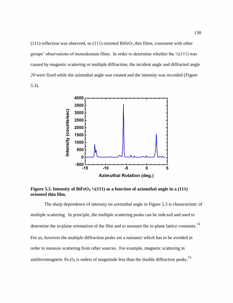
138
(111) reflection was observed, so (111) oriented BiFeO3 thin films, consistent with other
groups‟ observations of monodomain films. In order to determine whether the ½(111) was
caused by magnetic scattering or multiple diffraction, the incident angle and diffracted angle
2θ were fixed while the azimuthal angle was rotated and the intensity was recorded (Figure
5.3).
Figure 5.3. Intensity of BiFeO3 ½(111) as a function of azimuthal angle in a (111)
oriented thin film.
The sharp dependence of intensity on azimuthal angle in Figure 5.3 is characteristic of
multiple scattering. In principle, the multiple scattering peaks can be indexed and used to
determine the in-plane orientation of the film and to measure the in-plane lattice constants.14
For us, however the multiple diffraction peaks are a nuisance which has to be avoided in
order to measure scattering from other sources. For example, magnetic scattering in
antiferromagnetic Fe3O4 is orders of magnitude less than the double diffraction peaks.15

139
5.3. Forbidden ½{111} reflections in thin films
We observed Bragg reflections at pseudocubic ½{111} wavevectors. First, reciprocal
space maps of the BiFeO3, SrRuO3, and SrTiO3 (111) reflections were acquired to obtain an
estimate of the domain populations and to find the angular splitting of the BiFeO3 {111}.
The intensities of these reflections were also used as a baseline for comparing calculated
scattering factors to observed intensities. The incident angle was varied as a series of two-
dimensional diffraction patterns were recorded with a CCD detector. The intensity in each
image was summed over the out-of-plane direction (del) to give a 2D reciprocal space map.
One such map of the BiFeO3 {111} reflections from sample B3-2 is shown in Figure 5.4.
The focused synchrotron x-ray beam had a photon energy of 7.1 keV. The intensity is plotted
as a function of qx and qz,where |q| is in units of 1/d. The sample was aligned on the
diffractometer such that the qx was nearly parallel to the SrTiO3 [110] direction and qz was
parallel to the SrTiO3 [111] direction.
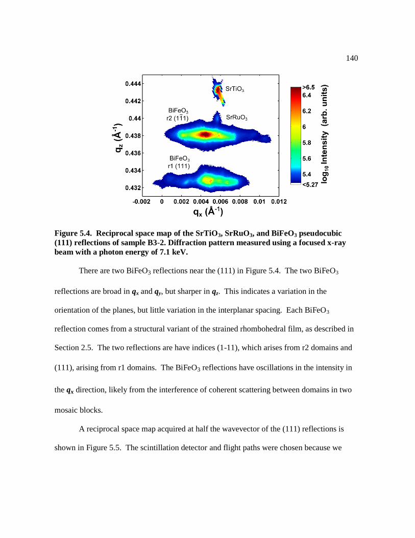
140
Figure 5.4. Reciprocal space map of the SrTiO3, SrRuO3, and BiFeO3 pseudocubic
(111) reflections of sample B3-2. Diffraction pattern measured using a focused x-ray
beam with a photon energy of 7.1 keV.
There are two BiFeO3 reflections near the (111) in Figure 5.4. The two BiFeO3
reflections are broad in qx and qy, but sharper in qz. This indicates a variation in the
orientation of the planes, but little variation in the interplanar spacing. Each BiFeO3
reflection comes from a structural variant of the strained rhombohedral film, as described in
Section 2.5. The two reflections are have indices (1-11), which arises from r2 domains and
(111), arising from r1 domains. The BiFeO3 reflections have oscillations in the intensity in
the qx direction, likely from the interference of coherent scattering between domains in two
mosaic blocks.
A reciprocal space map acquired at half the wavevector of the (111) reflections is
shown in Figure 5.5. The scintillation detector and flight paths were chosen because we

141
could detect weaker diffracted signals in this way. Reflections at the ½(111) from r1 domains
and ½(1-11) from r2 domains were observed.
Figure 5.5. Reciprocal space map of ½(1-11) and ½(111) BiFeO3 reflections from sample
B3-2.
The intensities of the ½{111} reflections were compared to the {111} reflections in
order to relate calculated structure factors to real intensities. The ½(1-11) reflection is more
intense and much broader than the ½(111) reflection. The ½(111) reflection is 2×10⁻⁴
times
the intensity of the (111); the ½(1-11) is 1×10⁻³
times the intensity of the (1-11). Although
the intensity of these reflections varied at different positions on the sample, the ½(1-11) was
always observed to be brighter than the ½(111) at all positions that we probed in the 400 nm
film. Based on the observed intensities of the {111} reflections, we predicted that magnetic
scattering reflections would have intensities of 0.5 counts per second. The reflections
observed here were 1,000 times more intense than the magnetic scattering signal, making it

142
extremely difficult to probe the magnetic ordering using x-ray diffraction. Thus we have
considered other possible origins of the high-intensity ½{111} reflections.
We determined that multiple scattering is does not occur in (001)-oriented BiFeO3
films by measuring the intensity of the ½(111) as a function of azimuthal angle. The
mounting wedge made it impossible to scan about the surface normal on the kappa
diffractometer at Sector 2-ID-D. The mu rotation is a good approximation for the azimuth for
small angles, but at large angles the incident angle is changed by increasingly larger amounts.
Scans of mu versus peak intensity show a slow decrease in intensity caused by gradually
changing the incident angle (Figure 5.6).
-2.0 -1.5 -1.0 -0.5 0.0 0.5 1.0 1.5
0
50
100
150
200
250
300
350
Inte
nsit
y (
co
un
ts/s
ec)
Azimuthal Rotation (deg.)
Figure 5.6. Dependence of diffracted intensity at the ½(111) on azimuthal angle in a 600
nm (001) BiFeO3 film (B-180-C).
The intensity of the ½(111) is not sharply dependent on the azimuthal angle. It
decreases large rotations of the azimuthal angle similar to any other Bragg reflection because

143
of the gradual change in incident angle of the x-rays. The ½(111) is thus not caused by
multiple scattering in the (001) thin films.
Structure factor calculations for charge scattering predict zero intensity at the ½{111}
family of reflections. These calculations used the atomic positions for BiFeO3 reported in
Kubel and Schmidt and the structure factor of Chapter 1.8 It should be noted that these
reflections are forbidden in R3c symmetry and no charge scattering is expected at these
wavevectors. The large intensity of the ½{111} reflections suggests that there is a structural
distortion that is unaccounted for in atomic positions found by neutron diffraction studies.
Using the ratio of intensity for the ½(111) to that of the (111), we found that the observed
intensity of the ½(111) corresponds to 18.8 r02, or approximately equal to the scattering from
an arrangement of four electrons with this periodicity.
5.4. ½{111} reflections in bulk BiFeO3
We wanted to determine if the structural distortion causing these reflections was
related to epitaxial strain. We measured the ½{111} reflections in a thicker (001) film and a
bulk sample of BiFeO3. Epitaxial strain can change the symmetry and atomic structure of a
thin film and might induce structural distortions unique to thin films. To determine the
effects of varying strain states, we measured half order reflections from a 600 nm (001) film
and a bulk crystal.
The 600 nm film had reflections at the ½(111) similar but not identical to the 400 nm
film. Reciprocal space maps were acquired near the BiFeO3 ½(111), (111), and ½(333)

144
Bragg reflections (Figure 5.7). The photon energy was chosen to be below the Fe K edge (7.1
keV) in order to reduce background scattering. The intensity at each point in qx and qz is
plotted as a function of color, where the color bar to the right of each map relates count rate to
color. Attenuators were necessary for the allowed Bragg reflections. The intensities in the
plots of Figure 5.7 were normalized to the intensity simultaneously measured with an ion
chamber so the attenuation factor is accounted for.
The 600 nm film serves as a comparison because it is more relaxed than the 400 nm
film but has not completely relaxed to the bulk lattice parameters. We find that the unmixed
½(111) reflection in the 600 nm film is weaker than that of the 400 nm film. Accurately
comparing intensities can be extremely complicated, however. The intensity of a thin film
Bragg reflection measured with a small beam is affected by the domain population inside the
diffraction volume, the reflection‟s structure factor, and the orientation of the mosaic block
with respect to incident x-ray beam. We measured the {111} reciprocal space map in several
places on the sample and consistently found that the (111) reflection was brighter than the (-
111) reflection. The intensities (Fhkl ∙F*hkl) for the mixed index peaks are calculated to be
approximately 20% higher than for the unmixed reflections. The reciprocal space map was
taken with detector slits that had an acceptance of about 1° in the direction perpendicular to
the scan of the plane (roughly equivalent to the chi rotation of the sample), which was large
enough to accept both reflections. After accounting for domain populations, rotations of the
mosaic blocks, and structure factor differences, we conclude that the ½(111) in the 600 nm
film is weaker than in that of the 400 nm film. This indicates that strain changes the
magnitude or direction of the distortions causing the ½{111} reflections.

145
Fig
ure 5
.7. R
eci
procal
space
map
s of
the ½
(111),
(111),
an
d ½
(333)
BiF
eO
3 B
ragg r
efl
ecti
on
s fr
om
th
e 6
00 n
m
BiF
eO
3 t
hin
fil
m. T
he c
en
ter p
lot
has
a s
ign
ific
an
tly l
arger i
nte
nsi
ty s
cale
th
an
th
e o
ther t
wo p
lots
sin
ce t
he (
111)
refl
ecti
on
s are t
hre
e o
rd
ers
of
magn
itu
de b
rig
hte
r t
han
th
e ½
(111
) an
d ½
(333).
T
he w
hit
e s
ecti
on
in
th
e ½
(333)
plo
t
is l
eft
in
ten
tion
all
y b
ecau
se t
he s
can
did
not
cover t
he p
orti
on
of
recip
rocal
space
con
tain
ing o
ne o
f th
e e
xp
ecte
d
refl
ecti
on
s.

146
The thin films are strained and misfit defects are introduced during the relaxation
process which may contribute to the intensity of the ½{111} type reflections. To determine
whether the half order reflections are a byproduct of epitaxial constraints or the relaxation
process, the same reflections were measured in an unstrained bulk BiFeO3 crystal. The bulk
sample contained all four structural variants described in section 2.5.1. Measurements with
an unfocused beam show that the sample contains more of variant r1 than of the other three.
The scattering geometry was designed such that the (111) planes of the r1 variant were in the
scattering plane. We observed ½{111} reflections from the r2, r3, and r4 variants which
were aligned to diffract from the ½(-111), ½(-1-11), and ½(1-11), respectively. These three
reflections had the same interplanar spacing and diffract at the same 2θ. A two-dimensional
scan of the incident angle and the detector‟s out of plane angle del measured a plane in
reciprocal space which cut through the center of all three mixed reflections (Figure 5.8).
Figure 5.8. Reciprocal space map at constant 2θ of the mixed ½ (-111), ½ (-1-11), and
½(1-11) reflections in bulk BiFeO3.

147
In the bulk sample, the ½{111} reflections were less intense than in the 600 nm film.
Count rates were normalized to the {111} reflections to compare intensities accurately.
Measurements taken at the synchrotron at 7.1 keV failed to detect the unmixed ½(111)
reflection. Figure 5.9 is a reciprocal space map showing two of the three possible mixed
reflections, along with the theoretical position of the unmixed ½(111) reflection.
The red circles in Figure 5.9 indicate the theoretical positions of scattering from the
spin spiral found in bulk BiFeO3. Neutron diffraction studies of the magnetic ordering in
bulk BiFeO3 show a spiral modulation of the spin direction within the (111) plane with a
period of 62 nm.16,17
Non-resonant scattering from the spin spiral in the bulk is possible as
well – satellite peaks at q1/2(hkl) ± qspiral are marked with red circles. None of these reflections
were found in the bulk at this energy. If the unmixed reflection is present, it at least 105
times less intense than the (111) reflection.
Figure 5.9. Reciprocal space map of the 1/2(-111) and 1/2(-1-11) reflections in bulk
BiFeO3. Red circles indicate the theoretical position of the ½(111) reflection and
satellite reflections from the magnetic spin spiral.

148
Although synchrotron microdiffraction reciprocal space maps did not find the ½(111)
reflection in the bulk, it was observed using a rotating anode x-ray diffractometer. The
½(111) was 3 counts per second, 10-5
times the (111) intensity. It is not immediately clear
why this reflection was observed using a rotating anode diffractometer but not with the
synchrotron measurements. One possibility is that the ½(111) reflection is dependent on the
iron scattering factor. The synchrotron measurements were conducted below the Fe K edge,
and the rotating anode experiments above the edge at 8.05 keV. If the intensity of the ½(111)
depends on the Fe scattering factor, then it would be more intense at energies above the Fe K
edge where f " is larger. Another possible explanation is that the diffraction volume for the
synchrotron measurements was small enough to completely miss the r1 structural variant that
produced the ½(111) reflection. The rotating anode has a large spot size of several square
millimeters, so the diffraction volume would be large enough to include all structural variants
and the ½(111) reflection was observed.
The pattern we observed is that the intensities of the ½{111} reflections increase with
epitaxial strain. The bulk had weak reflections, the 600 nm was less so, and the ones from the
400 nm film were brightest of all. The structural distortion causing these reflections is
increased in thin films, but the reflections from the bulk sample show that these distortions
are not caused by epitaxial strain alone. In order to quantify the relation between intensity
and strain, we applied a piezoelectric strain to the 400 nm film and measured the intensity of
the ½{111}.
149
5.5. Response of ½{111} reflections to piezoelectric strain
Time-resolved microdiffraction experiments determined that the intensities of the
½{111} reflections were proportional to piezoelectric strain. The ½{111} diffraction patterns
were measured while an electric field was applied to the 400 nm BiFeO3 (001) film. The
sample geometry was carefully chosen so the half order reflections from different structural
variants would be easy to identify. The sample was mounted so the (111) planes of r1
domains and the (1-11) planes of r2 domains were in the scattering plane. r1 and r2 type
domains made up the majority of ferroelectric domains in the as-grown state of this sample,
as discussed in Chapter 2. The sample was positioned so the focused beam diffracted only
from regions of BiFeO3 which were subjected to the electric field. The ½(111) has a larger
interplanar spacing than reflections with mixed positive and negative indices, so the reflection
at smaller 2θ can easily be indexed as ½(111) and the mixed reflection ½(1-11).
The intensity of the half order reflections was measured as a function of electric field.
The time resolved diffracted intensity was measured at each point in a scan of the incident
angle, θ. The detector angle 2θ was not scanned at the same time – instead the angular
acceptance of the detector was increased to 0.078°. The maximum applied electric field was
175 kV/cm, which changes 2θ by a maximum of 0.03°, estimated by calculating the strain
assuming piezoelectric constants of d33 = 53pm/V and d31 = 20 pm/V. The intensity at each
point is the sum of counts detected during a 1 ms window, repeated 1,000 times to give a total
counting time of 1 second. An example of the incident angle vs. time for field ranging from
0 to 175 kV/cm is shown below in Figure 5.10.

150
Figure 5.10. Response of ½(1-11) reflection to electric field in B3-2, the 400 nm film. (a)
Voltage applied to the top electrode as a function of time. This pulse was repeated 1,000
times in order improve counting statistics for the diffracted intensity. (b) Time resolved
intensity of ½(1-11) reflection. The intensity vs time (horizontal axis) was measured at
each point of an incident angle scan (vertical axis).
The peak intensity increased when the electric field was applied. The piezoelectric
strain induced peak shift was not measurable from these θ scans; the center of the peak was
predicted to shift by -0.015° and the scan step size was 0.052°. The ½(1-11) intensity
increases with electric field and is brightest in the center of Fig. 5.11(b). Structure factor
calculations for the allowed {111} reflections predict no change in intensity as a function of
electric field, assuming that the fractional coordinates of the atoms do not change. This is not
necessarily a valid assumption. Perovskite materials subjected to large strains have been
found to keep the bond lengths nearly constant for five B-O bonds at the cost of lengthening
the sixth.18,19
Holding bond lengths constant under strain changes the fractional coordinates,
which could account for the observed intensity change. To test this hypothesis, the intensity

151
of allowed reflections (111) and (1-11) as well as the ½(111) were measured as a function of
electric field.
Quantitative values for the intensity change were calculated by summing over the θ
scan at each point in the time scan to give integrated intensity versus electric field. The
electric field dependence for two ½{111} reflections and their corresponding {111}
reflections are plotted below in Figure 5.11. Change in intensity was calculated as a
percentage of the intensity near E = 0, taken to be the average of the intensities at 0 ms and 20
ms.
Figure 5.11. Change in intensity of (111), (1-11), ½(111), and ½(1-11) reflections versus
electric field.
The intensity of three out of the four reflections increases proportionally with the
applied electric field. Only the (111) reflection does not measurably increase in intensity.
The integrated intensity of the (1-11) reflection increases by 5% at 150 kV/cm. These are
both allowed reflections which mainly consist of charge scattering, so the increased intensity

152
is caused by changes in the atomic positions within the unit cell. Atoms moved perpendicular
to the (1-11) plane, but stayed the same distance away from the (111) plane.
The half-order reflections both increased more than the corresponding {111}
reflections. The ½(1-11) reflection increased by 26%, more than any other reflection. The
unmixed ½(111) also increases, but was difficult to accurately estimate the percent change at
150 kV/cm because of poor counting statistics. A least squares fit to a linear function
estimates the maximum change to be 4.5%. The ½(111) was very weak, so we had to count
for longer amount of time in order to measure the change. Longer counting times meant more
pulses applied to the sample. 260,000 pulses had to be applied for the scan shown above.
Applying this many low frequency pulses to the sample increased the leakage current. Large
current through the film leads to dielectric breakdown and the development of a conducting
paths which short the capacitor structure.
The linear response to electric field suggested the intensity change was related to
strain. Strain is hysteretic with electric field, so we applied a field antiparallel to the
polarization direction to see if the intensity change was hysteretic also. The intensity of the
½(1-11) reflection was measured for electric fields from -150 kV/cm to +250 kV/cm. The
fractional change as a function of field was calculated as described above and the results are
shown in Figure 5.12.

153
-250 -200 -150 -100 -50 0 50 100 150 200 250
-10
-5
0
5
10
15
20
25
30
35
40
% C
han
ge In
ten
sit
y
Applied Electric Field (kV/cm)
+10V positively poled
+6V positively poled
-6V, negatively poled
-4V, positively poled
Figure 5.12. Intensity of ½(1-11) versus electric field. The intensity is hysteretic with
electric field. The maximum voltage applied to the top electrode and the poling
direction for each scan is listed in the legend.
The intensity of the ½(1-11) reflection exhibits hysteresis with electric field. The
intensity increases when the polarization direction is parallel to the applied field, and
decreases when they are antiparallel. The response is not symmetric about E=0 because the
coercive field on the positive direction is much smaller than in the negative direction. No
data for negative polarization direction and positive electric field are available because the
polarization switched before the measurement could be completed.
The proportional increase in intensity and hysteretic response strongly suggests that
the order parameter responsible for the half order reflections is coupled to the piezoelectric
strain. Although the distortion is enhanced with increasing strain, it is not caused by
epitaxial strain alone, since the ½{111} reflections are also observed in bulk BiFeO3.
154
In order to determine which electrons contributed to the ½{111} reflections, we
measured the intensities of the half order reflections as a function of energy near the Fe K
edge. We observe a resonant enhancement of the intensity near the Fe K edge, demonstrating
that scattering from electrons bound to the iron contributes to the ½{111} reflections.
5.6. Resonant diffraction and chemical shift of ½{111} reflections
The energy dependence of a diffraction peak gives information about the atomic
scattering factors, absorption coefficients, and bonding states of the scattering electrons.
Measuring the integrated intensity of a reflection near an absorption edge can give element
specific information. The scattering factors dramatically increase at an absorption edge,
enabling the experimenter to determine which electrons are contributing to a given reflection.
In order to probe the source of scattering at the ½(111) reflection, we measured the intensity
as a function of photon energy near the Fe K edge.
Previous x-ray absorption studies of BiFeO3 thin films and powders show that the Fe
K edge in BiFeO3 shifts to higher energies than in pure Fe.20
The intensity of the x-ray
reflection depends on the atomic scattering factors. The imaginary part of the dispersion
correction, f ", is proportional to the absorption cross section. The intensity of reflections that
depend on the iron scattering factor is expected to dramatically change at transition edges.
The previous studies also reveal a small peak in the absorption at 7.11 keV, below the
observed K edge.20
This peak corresponds to the Fe 1s →3d transition, which is forbidden to
electric dipole transitions.

155
We measured the intensity of the ½(111) as a function of energy in the (111) film and
the 600 nm (001) film. θ-2θ scans over the reflections were taken at each photon energy. The
undulator energy was tuned to 7.1 keV and was held fixed during energy scans. The
undulator produces the most photons at the tuning energy, but the bandwidth is large enough
to create appreciable intensity, even at energies of approximately 50 eV from the photon
energy with highest intensity.21
The incident beam energy was scanned by changing the
monochromator angle. The monochromator was calibrated by measuring the intensity of x-
rays transmitted through a Fe foil and varying the energy over the Fe K edge at 7.112 keV.
Figure 5.13. Intensity of ½(1-11) reflection versus energy for the 600 nm (001) film and
the intensity of the ½(111) reflection from the (111) film. Dotted lines indicate the
energies of electronic transitions near the Fe3+
K edge in powder BiFeO3 measured using
XANES (from Lee et al.20
). The ½(111) reflection from the (111) film increases in
intensity at the absorption edges in the powder sample. The ½(111) reflection from the
(001) film increases intensity at a much lower energy.

156
We find that the intensity of the ½(1-11) reflection increased near the Fe K edge.
Figure 5.13 is a plot of the integrated intensity of half order reflections as a function of x-ray
photon energy. The multiple scattering ½(111) reflection from the (111) oriented BiFeO3
film was acquired with an unfocused beam and is a measure of charge scattering from
allowed reflections. The ½(1-11) reflection in the (001) film B-180-C was measured using a
focused beam. This indicates that the electrons contributing to this reflection are excited into
Fe orbitals. There is some modulation of these electrons which scatters x-rays at the ½(1-11)
wavevector. The resonant enhancement at the Fe K edge implies that these electrons are
bonded to the iron cations.4
Accurately comparing the intensities at different energies is complicated because the
performances of the undulator, monochromator, and ion chamber all depend on photon
energy. For example, the counting efficiency (number of counts per photon) of a typical ion
chamber using nitrogen gas will change by 10% over the 100 eV range scanned here.22
Since
we did not measure the energy dependent characteristics of the monochromator or the ion
chambers, intensities are simply normalized to the current in the storage ring. Each point in
Figure 5.13 represents the summed intensity over a θ-2θ scan at a given energy, normalized to
the storage ring current.
The (111) films also show a resonant enhancement of the intensity of the ½(111)
reflection at the Fe3+
K edge and at the pre-edge peak. The increase in intensity from the
(001) film is shifted by about 200 eV and shows no pre-edge peak. Measurements at
different locations on the sample all increase in intensity at 7.085 keV, although the width of
the resonant enhancement varies. The intensity variations above 7.09 keV are different at

157
each place on the sample. This suggests that the local bonding environment of atoms
contributing to the ½(111) reflection is inhomogeneous.
Variations in local bonding environments can be caused by any change in the lattice.
For example, atoms near a Frenkel defect, twin boundary, or miscut dislocation have different
bonding states than in the middle of a bulk single crystal.23
Oxygen vacancies could be
responsible for variations in the local bonding. Mixing between the O 2p orbital and Fe 3d
orbitals have been reported in materials like Fe2O3 which also contain octahedrally
coordinated Fe3+
ions.24
An oxygen vacancy site would shift the energy states of neighboring
Fe3+
ions, affecting the resonant scattering at the pre-edge feature.25
The resonant enhancement near the Fe K edge in Figure 5.13 indicates that some of
the electrons contributing to the ½(111) are either bound to iron or are part of a covalent bond
with iron. The ½(111) of the BiFeO3 film has a resonant enhancement at 7.08 keV, indicating
that these electronic states are different from those contributing to multiple scattering. The
intensity of the ½(111) versus photon energy was measured at several places on the sample
surface with the focused beam. The onset of the resonant enhancement always started at 7.08
keV, but the width of the peak varied. Changes in the resonant enhancement at different
places in the (001) film show that the electronic states vary spatially as well.
5.7. Structural distortion models for ½(hkl) reflections
The ½{111} and ½{333} reflections are a signature of a distortion of BiFeO3 from the
reported R3c symmetry. We considered three possible sources of scattering which would

158
contribute to the observed intensity at the half order reflections: antiparallel cation
displacements, rotations of the oxygen octahedra, and anisotropy in the atomic scattering
factors. Structure factors for each model were calculated for the ½{111} reflections. The
details of each model are discussed below, along with the supporting and detracting evidence.
We believe antiparallel cation displacements to be the most likely source of scattering at the
½{111} reflections.
5.7.1. Antiparallel cation displacements
Moving two cations in neighboring perovskite unit cells in opposite directions breaks
the symmetry and can produce reflections at ½(hkl) wavevectors. The structure factor of a
modified unit cell with antiparallel displacements of the iron ions was calculated. I focused
on displacements of the Fe3+
cation because of the resonant enhancement of the ½(1-11)
intensity near the Fe K edge. Displacements within the (111) plane were ruled out because
they produced no intensity for the ½(111) reflection. Cation displacements of 0.1 Å in
opposite directions along the [111] and [001] directions produce reflections a factor of 104
to105 times less intense than the {111} type reflections, similar to what we observe in the
bulk. Displacements of 0.2 Å produce half order reflections 103 times less than the intensity
of the {111} family of reflections. These intensities are similar to the intensity of the ½(1-11)
reflection observed in the 400 nm film. Antiparallel displacements of Fe ions could be the
structural distortion that causes the ½{111} reflections.
Charge disproportionation is known to cause displacements of the B site cations in
perovskite materials. Charge disproportionation is a redistribution of charge such that two
159
chemically distinct sites exist for one element in the material. It is observed in some
perovskite materials including BaFeO3,26
CaFeO3,27
BaBiO3, 28
and YNiO3.29
In hexagonal
BaFeO2.91, oxygen deficiencies are accommodated by charge disproportionation of the iron
ions, which nominally have a 4+ oxidation state.26
Alternating sheets of Fe+4+r
and Fe+4-r
parallel to the hexagonal (001) planes are formed. The different valences affect the Fe-O
bond length; Fe+4+r
ions have shorter bond lengths due to increased Coulombic repulsion and
Fe+4-r
ions have longer bond lengths.
We propose that the ½{111} reflections in BiFeO3 are a signature of antiparallel
displacements of the iron cations induced by a reordering of charge, similar to charge
disproportionation. In BiFeO3 thin films, oxygen vacancies change the oxidation state of the
neighboring cations from Fe3+
to Fe2+
. Iron ions with a nominal 2+ valence would be
displaced from the atomic positions in the rest of the film, so that they had longer bond
lengths than those with Fe3+
valence states. Ordering of these displacements would produce a
reflection at the ½(111). The intensity would be dependent on the atomic scattering factors of
Fe2+
and Fe3+
ions. Our observations of the resonant intensity of the ½(111) near the Fe K
edge are consistent with this explanation. The dispersion correction f " of octahedrally
coordinated Fe3+
in Fe3O4 has a peak below the Fe K edge which is 200 eV wide.30
The
enhancement of the ½(111) between 7.0 and 7.2 keV would be explained by this resonance.

160
5.7.2. Anisotropic octahedral rotations
Structure factors for BiFeO3 with several variations of rotation patterns of the oxygen
octahedra were calculated in order to determine whether these rotations could be responsible
for the ½ {111} and ½{333} reflections. In bulk BiFeO3, oxygen octahedra in neighboring
unit cells are rotated in opposite directions about the [111]pc axis. When the rotations about
each axis are exactly equal, the ½(hhh) reflections are not allowed. When the rotations are
anisotropic, however, the ½(111) is slightly allowed. Hatt and Spaldin suggest anisotropic
rotations of octahedra may help relieve small amounts of strain in perovskite films, even on
cubic substrates.31
The BiFeO3 films are known to relax anisotropically because of the
miscut of the SrTiO3 substrate, so anisotropic rotations of the octahedra are likely as well.
In order to test this hypothesis, we calculated the structure factor of a modified
perovskite cell in which the oxygen octahedra were rotated anisotropically. The positions of
atoms in 2×2×2 pseudocubic unit cells of BiFeO3 were calculated using the Megaw
program.32
Atomic positions were calculated by modifying a pseudocubic structure to
include Fe3+
displacements, the interaxial angle of 89.4°, and rotations of the oxygen
octahedra about the a, b, and c pseudocubic axes. The positions of the oxygen atoms were
calculated as a function of octahedral rotation angles. The lattice constants a, b, and c were
sets to the pseudocubic bulk value of 3.96 Å. The intensity of the ½{111} reflections were
calculated using these new oxygen positions. When the rotations about the a, b, and c axes
are all different, the structure factor for ½(111) reflections is non-zero. For example,
rotations of 5°, 15°, and 20° (tilt system a-b
-c
-) produce reflections 10
5 to 10
6 times less than
161
the {111} reflections. Many tilt patterns were tested, but the intensity of the ½(111)
reflection no more than 10-5
times the intensity of the (111). While anisotropic rotation may
contribute to the reflections we observe, they make up no more than 10% of the ½(111)
intensity found in the 400 nm BiFeO3 film.
We conclude that anisotropic rotation of the oxygen octahedra induced by epitaxial
strain is not the sole source of scattering at the ½{111} reflections in BiFeO3. Firstly, the
rotation angles required to produce just 10% of the observed intensities are quite large.
Secondly, the ½{111} reflections are still observed in the bulk sample that has no epitaxial
strain at all. While anisotropic rotation of the oxygen octahedra may contribute to the
intensity of the half order reflections, it is not the only source of scattering.
5.7.3. Anisotropic scattering factors
Anisotropy in atomic scattering factors causes reflections at ½(hkl) wavevectors.
Anisotropy in the electronic susceptibility at x-ray frequencies makes the atomic scattering
factor anisotropic as well.33,34
The atomic scattering factor is commonly assumed to depend
on photon energy and the magnitude, but not the direction, of q. In fact, the atomic scattering
factor is a tensor property which does depend slightly on the direction of q for several
reasons, such as point defects and anisotropy in thermal vibrations.33
The tensor nature of f
can usually be ignored because the anisotropy is very small in the x-ray region, but it
becomes more relevant near resonant energies. However, when the atomic scattering factor
tensor has a lower symmetry than the unit cell, forbidden reflections can appear. Forbidden

162
reflections in YVO3 caused by anisotropic scattering factor show a resonant enhancement
near the vanadium K edge.35
We estimated the intensity of reflections in BiFeO3 from anisotropic scattering
factors. Dmitrienko suggests that the intensity of these reflections should be on the same
order as the change in x-ray absorption for different polarization directions.33
The absorption
at the Fe K edge in a BiFeO3 thin film was measured for s and p polarization of the x-rays by
Lee et al.20
At the maximum of the K edge reflection, the absorption changes by
approximately 12%. Using Dmitreinko‟s rule of thumb and Lee‟s measurement of μ, we
estimate a 12% change in f " of iron at the K edge. Assuming that f ' varies by a similar 12%,
the predicted intensity would then be about 16 r02. The observed reflections range from 16 to
20 r02 and match the predictions for anisotropic scattering factor reflections quite well at the
Fe K edge.
The anisotropy in the absorption coefficient vanishes at energies far from the edge,
however, along with the intensity of the forbidden reflection. The XANES data for BiFeO3
show that the polarization dependence of μ disappears within 10 eV of the resonant peaks.20
The resonant enhancement of ½(111) in Figure 5.13 is 50 eV wide. Furthermore, we observe
the ½(111) and ½(-111) in the bulk sample far from the Fe K edge at 8.05 keV at
approximately the same intensities as at 7.1 keV. Anisotropy in the scattering factors may
contribute to the resonant enhancement of the intensity near the Fe K edge, but it does not
explain the non-resonant scattering of the ½{111} reflections.

163
5.8. Discussion
There are multiple sources of scattering at the ½{111} and ½{333} reflections. These
reflections are more intense than expected for pure magnetic scattering. Non-resonant
magnetic scattering calculations predict that magnetic reflections should be 108 times less
intense than the {111} reflections. The observed half-order reflection intensities, however,
range from 105 to 10
3 times less than the {111} reflections. It should be noted that magnetic
scattering from antiferromagnetic Fe2O3 was observed to be one or two orders of magnitude
more intense than the calculated value. De Bergevin and Brunel found magnetic reflections
which were only five orders of magnitude less than the charge scattering.15
Even with this
additional „fudge factor‟, the observed intensities are still 10 – 1000 times too large to be
consistent with our magnetic scattering model. We conclude that there is another source of
scattering contributing to these reflections in addition to any non-resonant magnetic
scattering.
We eliminated several potential sources of scattering at the half order reflections.
Higher harmonic x-rays were excluded by selecting only detected x-rays with the correct
photon energy. Multiple scattering reflections were avoided by varying the diffraction
geometry and choosing samples with smaller coherent regions and larger mosaic spreads. We
chose reflections which did not have reflections from the pattern of octahedral rotations found
in the literature. Changes in the octahedral rotation pattern may be present and contribute to
the ½{111} reflection intensities, especially in the thin film samples. However, the
reflections are also observed in the unstrained bulk sample so octahedral rotations induced by

164
epitaxial strain cannot be the only cause. Anisotropy in the atomic scattering factors would
explain the intensity of these reflections near the Fe K edge. Far from the edge, this model
predicts that forbidden reflections are orders of magnitude weaker than the intensities we
observe at 7.08 and 8.05 keV. Differences in anisotropic scattering factors may contribute to
the intensity of the ½{111} reflections near the Fe K edge, but are negligible in non-resonant
scattering at these wavevectors.
Antiparallel displacements of the Fe3+
cations are consistent with our observations. In
order to test this hypothesis, more ½(hkl) reflections should be measured to accurately refine
the structure. Higher x-ray energies would allow access to many of these half order peaks.
This should be done for thin films as well as single crystal samples. Monodomain samples
will eliminate potential scattering from interference between coherent scattering of multiple
polarization domains. The thin film sample should be grown on an (001) SrTiO3 substrate
miscut along the [110] direction to select a single ferroelectric polarization domain.36
The
single crystal sample should be poled before x-ray measurements to switch the ferroelectric
domains into a monodomain state. In order to distinguish between antiparallel cation
displacements and anisotropic scattering factors, the variation of the ½{111} reflections
should be measured as a function of azimuthal angle.33
This experiment should be conducted
with a single crystal that has a large (111) face so the azimuthal rotation coincides with a
rotation axis of the goniometer.

165
5.9. Summary
Half order reflections were observed in epitaxial BiFeO3 thin films and bulk crystals
at wavevectors corresponding to a doubling of the perovskite unit cell. ½{111} and ½{333}
reflections are forbidden by the bulk R3c symmetry, but are commensurate with the
antiferromagnetic ordering. ½{113} type reflections were also observed and are the result of
rotations of oxygen octahedra.
½{111} reflections were characterized in order to determine their origin. The ½{111}
reflections are more intense in partially relaxed thin films than in bulk samples. The energy
dependence of the ½(111) intensity shows an enhancement at energies below the bulk BiFeO3
Fe3+
K edge. The integrated intensity of the ½(1-11) reflection is proportional to the
piezoelectric strain and even demonstrates a hysteretic effect when the electric field is
antiparallel to the polarization direction. The ½(111) intensity changes only slightly when
piezoelectric strain is applied.
A number of theories were explored in order to explain the unusually large intensity
of the ½{111} and ½{333} reflections. Multiple scattering was ruled out in the (001) films
by measuring the intensity dependence on azimuthal angle, but was found to be the origin of
the ½(111) in (111) oriented films. Magnetic scattering calculations predict that non-resonant
magnetic scattering contributes no more than 1% of the total intensity of these reflections in
the bulk sample and (001) thin films. Anisotropic oxygen octahedral rotations contribute no
more than 10% of the intensity found in thin film samples. Anisotropy in the atomic
scattering factors could account for the resonant enhancement of the ½(111) intensities near
the Fe K edge but it does not play a role in non-resonant scattering. The most likely cause is

166
antiparallel displacements of the Fe cations which are not included in current structural
refinements of BiFeO3. The antiparallel cation displacements could be caused by different
valence states of Fe ions as a result of oxygen vacancies, similar to the charge
disproportionation effect in BaFeO0.91. We conclude that the current understanding of
BiFeO3 structure is incomplete and there are additional distortions present which have a
periodicity twice the dimensions of pseudocubic unit cell, most likely of the iron and oxygen
octahedra.

167
5.10. Chapter 5 references
1 C. Michel, J.-M. Moreau, G. D. Achenbechi, R. Gerson, and W.J. James, “The atomic
structure of BiFeO3,” Solid State Commun. 7, 701 (1969).
2 R. Przeniosło, M. Regulski And I. Sosnowska, “Modulation in Multiferroic BiFeO3:
Cycloidal, Elliptical or SDW?,” Journal of the Physical Society of Japan 75, 084718 (2006).
3 M. Blume and D. Gibbs, “Polarization Dependence of Magnetic X-ray Scattering”, Phys.
Rev. B 37, 1779 (1988).
4 S. W. Lovesey and S. E. Collins, X-ray Scattering and Absorption from Magnetic Materials,
(Oxford Publishing, 1996).
5 M. Blume, “Magnetic Scattering of X-Rays”, J. Appl. Phys. 57, 3615 (1985).
6 D. Lebeugle, D. Colson, A. Forget, M. Viret, A. M. Battaille, and A. Gukasov, “Electric-
Field-Induced Spin Flop in BiFeO3 Single Crystals at Room Temperature”, Phys. Rev. Lett.
100, 227608 (2008).
7 Andrey Zheludov, website. Magnetic form factors on this site were calculated using
empirical formulae given in P. J. Brown, Magnetic form factors, Section 4.4.5, International
Tables for Crystallography Vol. C (A. J. C. Wilson, ed.), pp. 391-399.
https://protos.ethz.ch/neutron/research/resources/formfactor/index/edit/fe3.gif downloaded
7/4/2011.
8 F. Kubel, H. Schmid, “Structure of a Ferroelectric and Ferroelastic Monodomain Crystal of
the Perovskite BiFeO3.” Acta Cryst B. 46, 698 (1990).
9 S. Poot, “Goniometric Apparatus for an X-ray Diffractometer,” U.S. Patent number
3636347, (1972).
10 E. D. Dufresne, http://sector7.xor.aps.anl.gov/manuals/bicron.pdf, downloaded 6/6/2011.
11 A. M. Glazer, “The Classification of Tilted Octahedra in Perovskites,” Acta Cryst. B 28,
3384 (1972).
12 A.M. Glazer, “Simple Methods of Determining Perovskite Structures,” Acta Cryst. A 31 756
(1975).
168
13
D. Tinberg, R. L. Jonson-Wilke, D. D. Fong, T. T. Fister, S. K. Steiffer, Y. Han, I. M.
Reaney, and S. Trolier-McKinstry, “Octahedral tilt transitions in relaxed epitaxial
Pb(Zr1−xTix)O3 films”, J. Appl. Phys. 109, 094104 (2011).
14 S.-L. Chang, Multiple Diffraction of X-rays in Crystals, (Springer-Verlag, Berlin, 1984).
15 M. Brunel, F. de Bergevin, “Diffraction of X-rays by Magnetic Materials. II. Measurements
on Antiferromagnetic Fe2O3”, Acta Cryst. A 37, 324 (1981).
16 I. Sosnowska, T. Peterlin-Neumaier and E. Steichele, “Spiral magnetic ordering in bismuth
ferrite,” J. Phys. C: Solid State Phys. 15, 4835 (1982).
17 S. Lee, T. Choi, W. Ratcliff, R. Erwin, S. W. Cheong, and V. Kiryukhin, “Single
ferroelectric and chiral magnetic domain of single-crystalline BiFeO3 in an electric field,”
Phys. Rev. B 78, 100101 (2008).
18 A. J. Hatt, N. A. Spaldin and C. Ederer, “Strain-induced isosymmetric phase transition in
BiFeO3”, Phys. Rev. B 81, 054109 (2010).
19 S. Tinte, K. M. Rabe, and D. Vanderbilt, “Anomalous enhancement of tetragonality in
PbTiO3 induced by negative pressure”, Phys. Rev. B 68,144105 (2003).
20 D. Lee, M. G. Kim, S. Ryu, H. M. Jang, S. G. Lee, “Epitaxially grown La-modified BiFeO3
magnetoferroelectric thin films”, Appl. Phys. Lett. 86, 222903 (2005).
21 R. J. Dejus, I. B. Vasserman, S. Sasaki, and E. R. Moog, “Undulator A Magnetic Properties
and Spectral Performance,” Argonne National Laboratory Technical Bulletin, TB-45 (2002).
22 A.C. Thompson, “X-ray Detectors”, in X-ray Data Booklet, (Lawrence Livermore National
Laboratory, Berkeley, 2008). Information from the X-ray Data Booklet can be found online at
http://xdb.lbl.gov/ .
23 S. Karazhanov, Y. Zhang, L.-W. Wang, A. Mascarenhas and S. Deb, “Resonant defect
states and strong lattice relaxation of oxygen vacancies in WO3,” Phys. Rev. B 68, 233204
(2003).
24 D. M. Sherman, “The electronic structures of Fe
3+ coordination sites in iron oxides:
Applications to spectra, bonding, and magnetism,” Physics and Chemistry of Minerals 12, 161
(1985).

169
25
F. G. Requejo, J.M. Ramallo-López, A. R. Beltramone, L. B. Pierella, O. A. Anunziat, “Fe-
containing ZSM-11 zeolites as active catalyst for SCR of NOx Part II. XAFS characterization
and its relationshipwith the catalytic properties,” Applied Catalysis A 266, 147 (2004).
26 K. Mori, T. Kamiyama, H. Kobayashi, K. Oikawa, T. Otomo and S. Ikeda , “Structural
Evidence for the Charge Disproportionation of Fe4+
in BaFeO3,” Journal of the Physical
Society of Japan 72, 2024 (2003).
27 P. M. Woodward, D. E. Cox, E. Moshopoulou, A. W. Sleight, S. Morimoto, “Structural
studies of charge disproportionation and magnetic order in CaFeO3,” Phys. Rev. B 62, 844
(2000).
28 D. E. Cox and A. W. Sleight, “Mixed-Valent Ba2Bi
3+Bi
5+O6 - Structure and Properties vs
Temperature,” Acta Cryst. B 35, 1 (1979).
29 J. A. Alonso, J. L. Garcia-Munoz, M. T. Fernandez-Diaz, M. A. G. Aranda, M. J. Martinez-
Lope and M. T. Casias,“Charge disproportionation in RNiO3 perovskites: Simultaneous
metal-insulator and structural transition in YNiO3,” Phys. Rev. Lett. 82, 3871 (1999).
30 A. I. Frenkel, J. O. Cross, D. M. Fanning, and I. K. Robinson, “DAFS analysis of
magnetite,” J. Synchrotron Rad. 6, 332 (1999).
31 A. J. Hatt and N. A. Spaldin, “Structural phases of strained LaAlO3 driven by octahedral tilt
instabilities”, Phys. Rev. B 82, 195402 (2010).
32 A. M. Glazer, “MEGAW: Computation of the effect of rotating octahedra in perovskites,”
http://www.amg122.com/programs/page10.html, downloaded 6/1/2011.
33 V. E. Dmitrienko, “Forbidden Reflections due to Anisotropic X-ray Susceptibility of
Crystals”, Acta Cryst. A 39, 29 (1983).
34 A. Kirfel, A. Petcov and K. Eichhorn, “Anisotropy of anomalous dispersion in X-ray
diffraction,” Acta Cryst. A 47, 180 (1991).
35 T. A. W. Beale, R. D. Johnson, Y. Joly, S. R. Bland, P. D. Hatton, L. Bouchnoire, C.
Mazzoli, D. Prabhakaran, and A. T. Boothroyd, “Resonant x-ray scattering from the 4p
quadrupole moment in YVO3”, Phys. Rev. B 82, 024105 (2010).
36 H. W. Jang, D. Ortiz, S. H. Baek, C. M. Folkman, R. R. Das, P. Shafer, Y. Chen, C. T.
Nelson, X. Pan, R. Ramesh, and C. B. Eom, “Domain engineering for enhanced ferroelectric
properties of epitaxial (001) BiFeO3 thin films,” Adv. Mater. 21, 817 (2009).