epitaxial growth of cubic gd2o3 thin films on ge substrates
TRANSCRIPT

Journal of Physics Conference Series
OPEN ACCESS
Epitaxial growth of cubic Gd2O3 thin films on GesubstratesTo cite this article A Molle et al 2008 J Phys Conf Ser 100 042048
View the article online for updates and enhancements
You may also likeHigh-pressure synthesis crystal chemistryand physics of perovskites with smallcations at the A siteAlexei A Belik and Wei Yi
-
Atomic interface structure of bixbyite rare-earth sesquioxides grown epitaxially onSi(1 1 1)Michael Niehle and Achim Trampert
-
Tailoring of carrier concentration andengineering of band gap for Sn-dopedIn2O3 films by postirradiation of negativelycharged oxygen ionsYutaka Furubayashi Makoto MaeharaHisashi Kitami et al
-
Recent citationsInfluence of nanostructure formation onthe crystal structure and morphology ofepitaxially grown Gd2O3 on Si(001)Philipp Gribisch et al
-
Surface chemistry of rare-earth oxidesurfaces at ambient conditions reactionswith water and hydrocarbonsElccedilin Kuumllah et al
-
Low interfacial trap density and high-temperature thermal stability in atomiclayer deposited single crystal Y2O3n-GaAs(001)Yen-Hsun Lin et al
-
This content was downloaded from IP address 7712597137 on 13102021 at 0005
Epitaxial growth of cubic Gd2O3 thin films on Ge substrates
Alessandro Molle Claudia Wiemer Md Nurul Kabir Bhuiyan Grazia Tallarida and Marco Fanciulli
CNR-INFM Laboratorio Nazionale MDM via C Olivetti 2 I-20041 Agrate Brianza (MI) Italy
E-mail alessandromollemdminfmit
Abstract Gd2O3 thin films were grown on Ge (001) substrates by molecular beam epitaxy The epitaxial character of the film is demonstrated by electron diffraction during the growth The structural characterization of the films shows that the Gd2O3 forms a bixbyite polymorph with a (110) out-of-plane orientation The formation of bixbyite structured Gd2O3 is discussed in terms of the atomic arrangement of the oxide planes on the Ge(001) surface
1 Introduction Imparting an epitaxial character to the growth of thin oxide films with high dielectric constant (high-κ) might have important advantages for the integration in future electronic devices Firstly epitaxial films are expected to have a superior thermal stability since they are not affected by re-crystallization process involving the formation of electrically leaking grain boundaries Secondly the commensurate matching of the crystal oxide planes with the semiconductor substrate would allow to induce a defined interface with a stable configuration thus preventing the undesired formation of a low-κ interfacial layer [12] Compared to the case of the perovskite oxides on Si [1] the epitaxial growth of rare earth binary oxides might also benefit from intrinsically higher band gap and suitable band offsets [34] The Gd2O3 appears to be a good candidate to fulfill these requisites within the rare earth oxides since its intrinsic monovalent character imposes the defined stoichiometry of the sesquioxide thus avoiding the emergence of any other different stoichiometric species [5] The more stable orientation of the Gd2O3 single crystal is known to be the cubic (110) one with a bixbyite arrangement Such a structure has been observed in Gd2O3 thin films grown on (001) semiconductor substrates by molecular beam epitaxy [26] Very recently we demonstrated for the first time the possibility to grow epitaxial cubic (110) Gd2O3 films on Ge(001) substrates and to switch this crystalline phase to the monoclinic (100) for an oxide thickness higher than 8 nm [7] Our aim here is to report on a more detailed structural and compositional characterization of the cubic (110) phase of Gd2O3 thin films on Ge(001)
2 Experimental The oxide growth was carried out and in situ characterized inside an Omicron ultra high vacuum multi-chamber molecular beam epitaxy (MBE) system The key factor responsible for the epitaxial character of the oxide growth was the co-deposition of a pure Gd beam (rate of 1 Aringmin) with a molecular oxygen supply (partial pressure of 5x10⁻⁷ mbar) at a growth temperature of 450degC The film composition was examined by in situ x-ray photoelectron spectroscopy (XPS) provided by a conventional Mg Kα radiation source (12536 eV) with a pass energy of 50 eV for the full scale
IVC-17ICSS-13 and ICN+T2007 IOP PublishingJournal of Physics Conference Series 100 (2008) 042048 doi1010881742-65961004042048
ccopy 2008 IOP Publishing Ltd 1
spectra and of 20 eV for the high resolution scans around the Gd 4d and O1s XPS lines The film structure was deeply investigated by in situ reflection high energy (30 keV) electron diffraction (RHEED) monitoring and by ex situ x-ray diffraction (XRD) To minimize the impact of the surface roughness on the interface a superior degree of structural and chemical order on the Ge surface was achieved via several cycles of Ar ion sputtering at room temperature and annealing at 500degC This treatment induces extended (001) terminated terraces with a (2x1) reconstruction
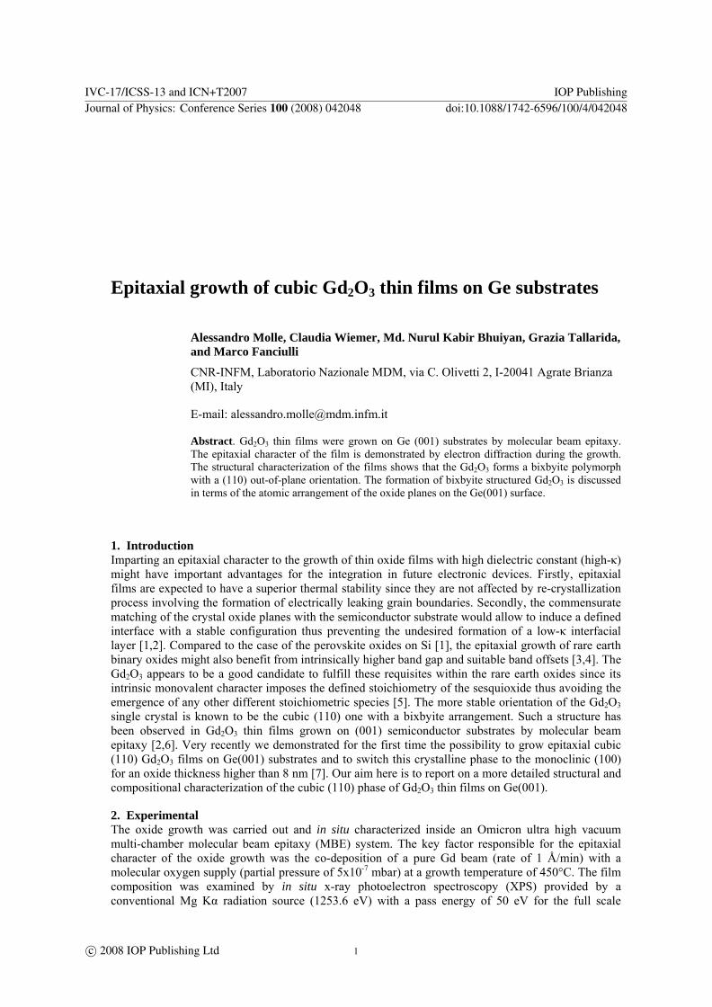
Figure 1 XPS analysis of a 7 nm thick Gd2O3 film a) Large scale XPS scan The photoemission lines inherent to the Gd2O3 and the signals due to the sample holder are marked as arrows and as SH respectively b) Gd 4d line fitted by a sixfold Voigt function accounting for the multiplet splitting in the two ionic state 7D and 9DJ (J=1hellip5) c) O 1s line fitted by a single Voigt function
3 Results and discussion The overall composition of the Gd2O3 films was checked by the XPS full scale scan reported in figure 1(a) for binding energies (BE) ranging from 0 to 900 eV The formation of Gd2O3 films is ensured by the distinct observation of the following selected XPS lines in the spectrum of figure 1(a) Gd 4f (BE=81 eV) Gd 4d (BE=1419 eV) Gd 4p (BE=273 eV) O 1s (BE=530 eV) and the O KVV1 Auger line (BE=7415 eV) The remaining shape profile of the spectrum can be due to the background or to photoemission from the substrate holder (SH) The ratio between the integrated intensities of the O 1s and Ge 4d XPS lines amounts to 152 upon rescaling on the relevant sensitivity factors [8] thus giving relative concentrations compatible with the Gd2O3 stoichiometry In detail the Gd 4d line is reported for a 7 nm thick Gd2O3 film in Figure 1(b) The shape profile of the spectrum is related to the multiplet splitting of the 4d hole with the 4f valence electrons to form 7D and 9D ionic states which are fitted respectively by a single broad Voigt function and by a five-fold Voigt contribution upon a Tougaard background removal [9] The O 1s line in Figure 1(c) is reproduced by a single Voigt peak at BE=530 eV which univocally points out the Gd-O bond homogeneity inside the oxide with no trace of hydroxide (Gd-OH) or germanate (Gd-O-Ge) presence The surface structure of the Gd2O3 stack was investigated by the in situ RHEED analysis for an oxide thickness of 27 nm (figure 2) The oxide growth was monitored by real time RHEED along the [110]Ge surface direction The Ge initial condition is illustrated as a reference in figure 2(a) by the RHEED streaky pattern endowed with remarkable half-order streaks (-frac120)Ge and (frac120)Ge indicating a well-defined (2x1) reconstruction of the Ge(001) surface structure After several seconds of deposition a new diffraction pattern appears which can be related to the formation of a crystalline Gd2O3 film In detail the RHEED pattern in figure 2(b1) is qualified by the twofold spot at both sides of the central (00) component which define two different surface lattice parameters identified by the reciprocal surface vectors g1 and g2
IVC-17ICSS-13 and ICN+T2007 IOP PublishingJournal of Physics Conference Series 100 (2008) 042048 doi1010881742-65961004042048
2
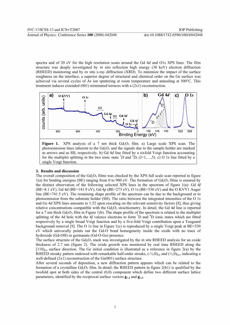
Figure 2 a) RHEED pattern of the as-prepared (2x1) reconstructed Ge(001) surface (the order of the streaks is marked) along the [110]Ge surface direction b1) RHEED pattern after the deposition of a 27 nm thick Gd2O3 film b2) 1D profile on the RHEED pattern in the b1) panel along the dotted line fitted by a multi-lorentzian function (aGe=2π aGe)
The exact spot position is extracted from the multiple lorentzian fit to the one dimensional (1D) cut to the RHEED pattern as shown in figure 2(b2) The 1D profile allows to compare the spot coordinates with the initial main (0n)Ge streaks (n=0plusmn1plusmn2hellip) sketched for clarity as vertical dashed lines The outer spots locate closely to the initial positions of first order Ge streaks (plusmn10)Ge thus suggesting a surface lattice constant almost similar to that of Ge along the Ge0]1[1 (aGe=4 Aring) The inner spots are placed at 1radic2 times the distance of the outer spots from the central peak The presence of two surface vectors suggests two contrasting in-plane orientations of opposite crystalline domains According to analogous RHEED observations on various epitaxial oxide films on Si(001) these features univocally claim for the formation of orthogonal domains with cubic (110) structure (bixbyite) [2] The identification of the oxide structure has also been deduced by the ex situ XRD scan in figure 3(a) taken on a 7 nm thick film which is clearly indicative of a Bragg signal from cubic (110) oriented planes of the oxide (Θ=47deg) on the (001) Ge surface plane (Θ=317deg) To have a thorough insight into the in-plane orientation of the Gd2O3 film XRD maps taken for a film thickness of 27 nm around the (111) oxide planes show the emergence of a Bragg peak for the azimuthal angles ϕ = 0deg and 90deg Therefore two in-plane epitaxial relationships can be equivalently deduced as follows A) [001]ox Ge0]1[1 B) [001]ox [110]Ge which unambiguously identify the coexistence of orthogonal cubic(110) domains typical of the bixbyite structure To rationalize how the Gd2O3 molecules accommodate on the Ge(001) surface plane the most likely bonding configuration at the interface level can be discerned from general considerations on the matching between a Gd2O3 fcc cubic cell with a flat (001) terminated Ge terrace A bare fcc cubic Gd2O3 lattice is made up of Gd atoms in the positions of a fcc lattice with a lattice parameter aGd=541 Aring intercalated with a simple cubic lattice of the O atoms with lattice constant aO=frac12 aGdasymp 271 Aring In analogy with the growth of Gd2O3 and Pr2O3 cubic films on Si(001) [210] we assume that the interface bonding configuration consists of Ge-O-Gd chains As for the Si case [2] the above assumption can be generally motivated by the chemical tendency of the Ge atoms to bind to the O atoms rather than to the Gd ones due to the high ionicity of the Gd-O bonds and to the relatively lower Ge-O bond length (18 Aring) Therefore the matching of the O atoms is a key point to understand the formation of the bixbyite structure If this is the case we should consider how the oxygen (110) planes of the oxide may fit to the Ge(001) surface The O(110) planes can arrange according to two equivalent in-plane orientations as displayed in the qualitative hard sphere sketches in figure 3(c1)-(c2) where the lattice constants of the cubic Gd2O3 bulk have been used without accounting for any lattice distortion The two different arrangements reflect the two epitaxial relationships A) and B)
IVC-17ICSS-13 and ICN+T2007 IOP PublishingJournal of Physics Conference Series 100 (2008) 042048 doi1010881742-65961004042048
3
deduced from the XRD map at perpendicular ϕ values thus providing a self-consistent picture of the bixbyite structured Gd2O3 films
Figure 3 a) XRD scan on a 7 nm thick Gd2O3 film showing the cubic(110) orientation b) XRD maps around the (111) oxide planes at ϕ=0deg and 90deg c1)-c2) hard sphere sketches of the two orientations of the O(110) oxide planes on the Ge(001) surface (take the red-coloured cells formed by the O atoms as a reference)
4 Conclusions We reported on the epitaxial growth of cubic (110) Gd2O3 thin films on Ge(001) substrates The film composition is consistent with the Gd2O3 stoichiometry according to the XPS analysis Below a thickness of 8 nm the films form a bixbyite structure qualified by the coexistence of mutually orthogonal domains with a cubic(110) registry The formation of the bixbyite structure has been rationalized in terms of the matching between the oxygen (110) planes of the oxide and the (001) terminated terraces of the Ge surface
5 Acknowledgement We acknowledge the partial financial support from the ET4US European Project
References [1] RA McKee FJ Walker and M F Chisholm Phys Rev Lett 81 3014 (1998) [2] H J Osten E bugiel M Czernohorsky Z Elassar O Kirfel and A Fissel Topics Appl Phys
106 101-114 (2004) M Fanciulli G Scarel Eds Springer (2007) [3] J Robertson Rep Prog Phys 69 327 (2006) [4] M Badylevich S Shamuilia V V Afanasrsquoev A Stesmans A Laha H J Osten A Fissel
Appl Phys Lett 90 252101 (2007) [5] G Adachi and N Imanaka Chem Rev 98 1479 (1998) [6] M Hong J Kwo A R Kortan J P Mannaerts A M Sergent Science 283 1897 (1999) [7] A Molle M N K Bhuiyan G Tallarida and M Fanciulli Appl Phys Lett 89 083504
(2006) [8] D Briggs and M P Seah Practical Surface Analysis Vol 1 Auger and X-ray photoelectron
spectroscopy Wiley 1990 [9] WJ Lademan A K See L B Klebanoff G Van der Laan Phys Rev B 54 17191 (1996) [10] H J Osten J P Liu E Bugiel H J Muessing P Zaumseil Mat Sci Engin B87 297 (2001)
IVC-17ICSS-13 and ICN+T2007 IOP PublishingJournal of Physics Conference Series 100 (2008) 042048 doi1010881742-65961004042048
4
Epitaxial growth of cubic Gd2O3 thin films on Ge substrates
Alessandro Molle Claudia Wiemer Md Nurul Kabir Bhuiyan Grazia Tallarida and Marco Fanciulli
CNR-INFM Laboratorio Nazionale MDM via C Olivetti 2 I-20041 Agrate Brianza (MI) Italy
E-mail alessandromollemdminfmit
Abstract Gd2O3 thin films were grown on Ge (001) substrates by molecular beam epitaxy The epitaxial character of the film is demonstrated by electron diffraction during the growth The structural characterization of the films shows that the Gd2O3 forms a bixbyite polymorph with a (110) out-of-plane orientation The formation of bixbyite structured Gd2O3 is discussed in terms of the atomic arrangement of the oxide planes on the Ge(001) surface
1 Introduction Imparting an epitaxial character to the growth of thin oxide films with high dielectric constant (high-κ) might have important advantages for the integration in future electronic devices Firstly epitaxial films are expected to have a superior thermal stability since they are not affected by re-crystallization process involving the formation of electrically leaking grain boundaries Secondly the commensurate matching of the crystal oxide planes with the semiconductor substrate would allow to induce a defined interface with a stable configuration thus preventing the undesired formation of a low-κ interfacial layer [12] Compared to the case of the perovskite oxides on Si [1] the epitaxial growth of rare earth binary oxides might also benefit from intrinsically higher band gap and suitable band offsets [34] The Gd2O3 appears to be a good candidate to fulfill these requisites within the rare earth oxides since its intrinsic monovalent character imposes the defined stoichiometry of the sesquioxide thus avoiding the emergence of any other different stoichiometric species [5] The more stable orientation of the Gd2O3 single crystal is known to be the cubic (110) one with a bixbyite arrangement Such a structure has been observed in Gd2O3 thin films grown on (001) semiconductor substrates by molecular beam epitaxy [26] Very recently we demonstrated for the first time the possibility to grow epitaxial cubic (110) Gd2O3 films on Ge(001) substrates and to switch this crystalline phase to the monoclinic (100) for an oxide thickness higher than 8 nm [7] Our aim here is to report on a more detailed structural and compositional characterization of the cubic (110) phase of Gd2O3 thin films on Ge(001)
2 Experimental The oxide growth was carried out and in situ characterized inside an Omicron ultra high vacuum multi-chamber molecular beam epitaxy (MBE) system The key factor responsible for the epitaxial character of the oxide growth was the co-deposition of a pure Gd beam (rate of 1 Aringmin) with a molecular oxygen supply (partial pressure of 5x10⁻⁷ mbar) at a growth temperature of 450degC The film composition was examined by in situ x-ray photoelectron spectroscopy (XPS) provided by a conventional Mg Kα radiation source (12536 eV) with a pass energy of 50 eV for the full scale
IVC-17ICSS-13 and ICN+T2007 IOP PublishingJournal of Physics Conference Series 100 (2008) 042048 doi1010881742-65961004042048
ccopy 2008 IOP Publishing Ltd 1
spectra and of 20 eV for the high resolution scans around the Gd 4d and O1s XPS lines The film structure was deeply investigated by in situ reflection high energy (30 keV) electron diffraction (RHEED) monitoring and by ex situ x-ray diffraction (XRD) To minimize the impact of the surface roughness on the interface a superior degree of structural and chemical order on the Ge surface was achieved via several cycles of Ar ion sputtering at room temperature and annealing at 500degC This treatment induces extended (001) terminated terraces with a (2x1) reconstruction
Figure 1 XPS analysis of a 7 nm thick Gd2O3 film a) Large scale XPS scan The photoemission lines inherent to the Gd2O3 and the signals due to the sample holder are marked as arrows and as SH respectively b) Gd 4d line fitted by a sixfold Voigt function accounting for the multiplet splitting in the two ionic state 7D and 9DJ (J=1hellip5) c) O 1s line fitted by a single Voigt function
3 Results and discussion The overall composition of the Gd2O3 films was checked by the XPS full scale scan reported in figure 1(a) for binding energies (BE) ranging from 0 to 900 eV The formation of Gd2O3 films is ensured by the distinct observation of the following selected XPS lines in the spectrum of figure 1(a) Gd 4f (BE=81 eV) Gd 4d (BE=1419 eV) Gd 4p (BE=273 eV) O 1s (BE=530 eV) and the O KVV1 Auger line (BE=7415 eV) The remaining shape profile of the spectrum can be due to the background or to photoemission from the substrate holder (SH) The ratio between the integrated intensities of the O 1s and Ge 4d XPS lines amounts to 152 upon rescaling on the relevant sensitivity factors [8] thus giving relative concentrations compatible with the Gd2O3 stoichiometry In detail the Gd 4d line is reported for a 7 nm thick Gd2O3 film in Figure 1(b) The shape profile of the spectrum is related to the multiplet splitting of the 4d hole with the 4f valence electrons to form 7D and 9D ionic states which are fitted respectively by a single broad Voigt function and by a five-fold Voigt contribution upon a Tougaard background removal [9] The O 1s line in Figure 1(c) is reproduced by a single Voigt peak at BE=530 eV which univocally points out the Gd-O bond homogeneity inside the oxide with no trace of hydroxide (Gd-OH) or germanate (Gd-O-Ge) presence The surface structure of the Gd2O3 stack was investigated by the in situ RHEED analysis for an oxide thickness of 27 nm (figure 2) The oxide growth was monitored by real time RHEED along the [110]Ge surface direction The Ge initial condition is illustrated as a reference in figure 2(a) by the RHEED streaky pattern endowed with remarkable half-order streaks (-frac120)Ge and (frac120)Ge indicating a well-defined (2x1) reconstruction of the Ge(001) surface structure After several seconds of deposition a new diffraction pattern appears which can be related to the formation of a crystalline Gd2O3 film In detail the RHEED pattern in figure 2(b1) is qualified by the twofold spot at both sides of the central (00) component which define two different surface lattice parameters identified by the reciprocal surface vectors g1 and g2
IVC-17ICSS-13 and ICN+T2007 IOP PublishingJournal of Physics Conference Series 100 (2008) 042048 doi1010881742-65961004042048
2
Figure 2 a) RHEED pattern of the as-prepared (2x1) reconstructed Ge(001) surface (the order of the streaks is marked) along the [110]Ge surface direction b1) RHEED pattern after the deposition of a 27 nm thick Gd2O3 film b2) 1D profile on the RHEED pattern in the b1) panel along the dotted line fitted by a multi-lorentzian function (aGe=2π aGe)
The exact spot position is extracted from the multiple lorentzian fit to the one dimensional (1D) cut to the RHEED pattern as shown in figure 2(b2) The 1D profile allows to compare the spot coordinates with the initial main (0n)Ge streaks (n=0plusmn1plusmn2hellip) sketched for clarity as vertical dashed lines The outer spots locate closely to the initial positions of first order Ge streaks (plusmn10)Ge thus suggesting a surface lattice constant almost similar to that of Ge along the Ge0]1[1 (aGe=4 Aring) The inner spots are placed at 1radic2 times the distance of the outer spots from the central peak The presence of two surface vectors suggests two contrasting in-plane orientations of opposite crystalline domains According to analogous RHEED observations on various epitaxial oxide films on Si(001) these features univocally claim for the formation of orthogonal domains with cubic (110) structure (bixbyite) [2] The identification of the oxide structure has also been deduced by the ex situ XRD scan in figure 3(a) taken on a 7 nm thick film which is clearly indicative of a Bragg signal from cubic (110) oriented planes of the oxide (Θ=47deg) on the (001) Ge surface plane (Θ=317deg) To have a thorough insight into the in-plane orientation of the Gd2O3 film XRD maps taken for a film thickness of 27 nm around the (111) oxide planes show the emergence of a Bragg peak for the azimuthal angles ϕ = 0deg and 90deg Therefore two in-plane epitaxial relationships can be equivalently deduced as follows A) [001]ox Ge0]1[1 B) [001]ox [110]Ge which unambiguously identify the coexistence of orthogonal cubic(110) domains typical of the bixbyite structure To rationalize how the Gd2O3 molecules accommodate on the Ge(001) surface plane the most likely bonding configuration at the interface level can be discerned from general considerations on the matching between a Gd2O3 fcc cubic cell with a flat (001) terminated Ge terrace A bare fcc cubic Gd2O3 lattice is made up of Gd atoms in the positions of a fcc lattice with a lattice parameter aGd=541 Aring intercalated with a simple cubic lattice of the O atoms with lattice constant aO=frac12 aGdasymp 271 Aring In analogy with the growth of Gd2O3 and Pr2O3 cubic films on Si(001) [210] we assume that the interface bonding configuration consists of Ge-O-Gd chains As for the Si case [2] the above assumption can be generally motivated by the chemical tendency of the Ge atoms to bind to the O atoms rather than to the Gd ones due to the high ionicity of the Gd-O bonds and to the relatively lower Ge-O bond length (18 Aring) Therefore the matching of the O atoms is a key point to understand the formation of the bixbyite structure If this is the case we should consider how the oxygen (110) planes of the oxide may fit to the Ge(001) surface The O(110) planes can arrange according to two equivalent in-plane orientations as displayed in the qualitative hard sphere sketches in figure 3(c1)-(c2) where the lattice constants of the cubic Gd2O3 bulk have been used without accounting for any lattice distortion The two different arrangements reflect the two epitaxial relationships A) and B)
IVC-17ICSS-13 and ICN+T2007 IOP PublishingJournal of Physics Conference Series 100 (2008) 042048 doi1010881742-65961004042048
3
deduced from the XRD map at perpendicular ϕ values thus providing a self-consistent picture of the bixbyite structured Gd2O3 films
Figure 3 a) XRD scan on a 7 nm thick Gd2O3 film showing the cubic(110) orientation b) XRD maps around the (111) oxide planes at ϕ=0deg and 90deg c1)-c2) hard sphere sketches of the two orientations of the O(110) oxide planes on the Ge(001) surface (take the red-coloured cells formed by the O atoms as a reference)
4 Conclusions We reported on the epitaxial growth of cubic (110) Gd2O3 thin films on Ge(001) substrates The film composition is consistent with the Gd2O3 stoichiometry according to the XPS analysis Below a thickness of 8 nm the films form a bixbyite structure qualified by the coexistence of mutually orthogonal domains with a cubic(110) registry The formation of the bixbyite structure has been rationalized in terms of the matching between the oxygen (110) planes of the oxide and the (001) terminated terraces of the Ge surface
5 Acknowledgement We acknowledge the partial financial support from the ET4US European Project
References [1] RA McKee FJ Walker and M F Chisholm Phys Rev Lett 81 3014 (1998) [2] H J Osten E bugiel M Czernohorsky Z Elassar O Kirfel and A Fissel Topics Appl Phys
106 101-114 (2004) M Fanciulli G Scarel Eds Springer (2007) [3] J Robertson Rep Prog Phys 69 327 (2006) [4] M Badylevich S Shamuilia V V Afanasrsquoev A Stesmans A Laha H J Osten A Fissel
Appl Phys Lett 90 252101 (2007) [5] G Adachi and N Imanaka Chem Rev 98 1479 (1998) [6] M Hong J Kwo A R Kortan J P Mannaerts A M Sergent Science 283 1897 (1999) [7] A Molle M N K Bhuiyan G Tallarida and M Fanciulli Appl Phys Lett 89 083504
(2006) [8] D Briggs and M P Seah Practical Surface Analysis Vol 1 Auger and X-ray photoelectron
spectroscopy Wiley 1990 [9] WJ Lademan A K See L B Klebanoff G Van der Laan Phys Rev B 54 17191 (1996) [10] H J Osten J P Liu E Bugiel H J Muessing P Zaumseil Mat Sci Engin B87 297 (2001)
IVC-17ICSS-13 and ICN+T2007 IOP PublishingJournal of Physics Conference Series 100 (2008) 042048 doi1010881742-65961004042048
4