digital design and verification of adaptive noise
TRANSCRIPT

PHUOC TAI VO
Digital Design and Verification of Adaptive Noise Cancellation Module
Metropolia University of Applied Sciences
Bachelor of Engineering
Degree Programme in Electronics Engineering
Bachelor’s Thesis
10 November 2020

Abstract
Author Title
PHUOC TAI VO Digital Design and Verification of Adaptive Noise Cancellation
Number of Pages Date
61 pages 10 November 2020
Degree Bachelor of Engineering
Degree Programme Electronics Engineering
Specialisation option Electronics
Instructor(s) Janne Mäntykoski, Senior Lecturer
Currently, at Metropolia University Applied of Sciences, digital design and implementation based on DSP studies have mainly focused on how to write efficient codes according to common coding styles rule. However, for its verification process before physical design, ver-ification with an HDL testbench is the only method which is instructed in university. Advanced and high-level verification methods, especially UVM, are still not applied for teaching and studies. Apart from that, when it comes to DSP implementation, adaptive filtering ap-proaches were selected to solve the interesting problem of how to track the statistical varia-tions of signal and eliminate random noise over time in a nonstationary environment with massive datasets and unstructured data types for complex hardware implementation. There-fore, the Thesis work aimed to design and implement an adaptive FIR filtering noise cancel-lation module based on LMS algorithm and verify its functional specifications. In the Thesis work, an adaptive noise cancellation module was developed to be well-pre-pared for hardware emulation. Module design and verification studied MathWorks workflow step by step. Matlab reference code was designed and optimized on algorithm level. Sim-ulink model which contains the fixed-point implementation was simulated to be compared with Matlab algorithm for periodic discrete-time environment before synthesizing into VHDL. The Register Transfer Level Design was verified in cosimulation with Simulink model. Be-sides, UVM based verification was applied to use System Verilog as verification language to evaluate the fulfillment of functional requirements and guarantee design accuracy with bit-cycle level. The Thesis presents the design module, which serves the purpose of noise cancellation based on adaptive LMS algorithm. The theory and mathematical model of the design module are explained. RTL reusability was achieved with the use of modular coding style to create instantiated functions. The implementation work was done adhering to Mathworks digital design flow. Additionally, no errors or bugs were found from the design module under verifi-cations. The module passed all required functionality tests. Hardware deployment and the related challenges, such as IP core generation to be integrated with a register abstraction layer, could be innovated for future development of this Thesis project, since the design module was already modified to be modular and reusable to form a scalable architecture with generic parameter specifications.
Keywords Adaptive filter, UVM, finite impulse response, digital design, RTL

Contents
List of Abbreviations 5
1 Introduction 1
2 Theory 3
2.1 Adaptive FIR Filtering 3
2.2 Least Mean Squares Algorithm 4
2.3 Adaptive Noise Canceller System 8
3 Digital Design Flow, Languages and Tools 9
3.1 Digital Design Flow 9
3.2 Hardware Design and Verification Languages 11
3.2.1 VHDL for RTL Design 11
3.2.2 System Verilog for Verification 11
3.3 Verification Flow and Universal Verification Methodology 12
4 Design Specifications and Algorithm to Architecture 17
4.1 LMS Algorithm for Digital Design and Implementation 17
4.2 Design Configurations and Constraints 20
4.2.1 Floating-point Matlab Implementation 20
4.2.2 Floating-point to Fixed-point Conversion 21
4.2.3 Coding Style 22
4.2.4 Verification Requirements 23
5 Adaptive FIR Filtering Noise Cancellation Module Implementation 24
5.1 Matlab Analysis and Implementation 24
5.1.1 Floating-point Matlab Implementation 24
5.1.2 Fixed-point Matlab Mathematical Testbench 30
5.2 Simulink Reference Modelling 31
5.3 Register Transfer Level Design with VHDL 38
6 Adaptive FIR Filtering Noise Cancellation Module Verification 42
6.1 HDL Testbench Generation and Simulation with Questa Sim 42
6.2 Code Coverage 45
6.3 HDL Cosimulation Verification 47

6.4 Functional Verification with Universal Verification Methodology 49
6.5 System Verilog Assertions 55
7 Conclusion 60
References 62

List of Abbreviations
ASIC Application Specific Integrated Circuit
AXI Advanced eXtensible Interface
DPI Direct Programming Interface
DSP Digital Signal Processing
DUT Design Under Test
DUV Design Under Verification
EDA Electronic Design Automation
FEC Focused Expression Coverage
FIR Finite Impulse Response
FPGA Field Programmable Gate Array
HDL Hardware Description Language
IEEE Institute of Electrical and Electronics Engineers
IIR Infinite Impulse Response
IP Intellectual Property
LMS Least Mean Squares
RLS Recursive Least Squares
RTL Register Transfer Level
SoC System On Chip

SV System Verilog
VHDL Very High Speed Integrated Circuit Hardware Design Language
UVM Universal Verification Methodology

1
1 Introduction
For the decades, the tremendous development in digital signal processing area which is
in relation to growing technologies allows digital design and hardware implementation of
signal processing to practically implement mathematical computations and complex
algorithms. If the signal statistics are available to define data properties, fixed algorithms
could be appropriately selected to be processed easily. Despite that, to track the
statistical variations of signal over time in a nonstationary environment, its algorithms to
be determined in advance are no longer efficient. The solution for this challenge is to use
adaptive filter that automatically adapts to input characteristics change and noise
cancellation by iterative estimation of configured parameters. Therefore, from this
motivation, the Thesis work was to implemented to present the overall process of how to
set up the adaptive noise cancellation module step-by-step from fixed-point conversion,
reference modeling, RTL design with HDL testbench integration and UVM-based
verification.
The goal of the Thesis work was to design, implement and verify an adaptive FIR filtering
noise cancellation module coded in hardware description language according to the
predefined design specifications and reference algorithms written by Matlab. The design
had to be configurable with modular coding style that it can be reused in future university
studies or innovation projects. Moreover, the design module is bit-exactly verified in UVM
test bench against the implemented fixed-point Simulink reference model with provided
configured parameters to confirm that the module is functioning bit-to-bit accurately as
specified.
The HDL of choice for the project was Very High Speed Hardware Description Language
version 1993, Institute of Electrical and Electronics Engineers standard 1076-1993.
VHDL was chosen for its proven reliability and manufacturability in designing Application
Specific Integrated Circuits and compatibility with virtually every commercially available
design and verification tool [19;11,9].
The verification language used in the project was System Verilog, IEEE standard 1800-
2005 [20]. SV is a higher-level, more versatile and less verbose language to design com-
plex test environments with. SV and VHDL can also interface with each other to an suf-
ficient degree and passing signals from design language to another is reasonably simple
to do. SV is also a widespread, standardized, well supported and documented HDL.

2
[11,9] The universal design methodology based test environment was written almost
completely in SV [21].
The mathematical algorithm is constructed to describe adaptive FIR filtering process for
noise cancellation. Matlab numerical computation based on the configured use case is
to generate compatible input sources then run its theoretical test to capture output data
for simulation graphical plots of the compared results. For floating-point to fixed-point
conversion, Simulink reference model is generated according to the verified Matlab al-
gorithm to be against the register transfer level description of the module during config-
ured sample time simulation run. This model was used for generating reference data
under DPI-C code format for the UVM testbench which HDL entities were binding during
parallel test simulation. The output data generated by RTL was compared to the data
output from the Simulink fixed-point mathematical model simulation.
The UVM test bench utilized was to verify DUT at bit level for test cycles and the elec-
tronic design automation tools used in verification management are capable of doing not
only thorough code coverage analysis but also functional assertions.

3
2 Theory
The theoretical background for the Adaptive FIR Filtering Noise Cancellation module is
presented in this chapter. The main theoretical concepts behind LMS design and brief
descriptions of how to operate adaptive noise cancellation in details are introduced.
2.1 Adaptive FIR Filtering
Adaptive filters are digital filters which have a set of coefficients to be changed under
step adaptations in order to reach to the optimal convergence [4,421]. Adaptive algorithm
would attempt to track the statistical changes in the input signals, the optimum solution
is dependent on its inherent convergence rate versus the speed of input data character-
istics [1,23]. The optimization criterion to be considered is the average mean square of
error difference between filter output and desired signal value. During filter coefficients
adaptation, the mean square error converges step-by-step to its minimal value. This state
is said to be the optimal state at which the filter output matches very closely to the desired
signal. According to the optimized algorithm, the determined transfer function is con-
trolled by variable parameters. It means the adaptive filters self-adjust with recursive
algorithm to compute updated filter weights. [1,30-31.]
Normally, when the signals start from some predetermined set of initial conditions to
know their priori information, it is simple to process with the fixed algorithm after a num-
ber set of iterations. But in a nonstationary environment, it no longer works as desired.
[1,22-23.] Due to the special nature mentioned above, especially the tracking capability
for time variation of input data, adaptive filter has been selected for practical use cases
and has become an important part of DSP applications like channel equalization, echo
cancellation or adaptive beamforming. The basic function comes down to the adaptive
filter performing a range of different tasks, namely, system identification, inverse system
identification, noise cancellation and prediction. [1,37-38.]
Although both IIR and FIR filters have been considered for adaptive filtering, the FIR filter
is by far the most practical and widely used. The FIR filter has only adjustable zeros to
guarantee filter stability without the need of poles adjustments as in adaptive IIR filters.
That is, adaptive FIR filters are always stable. [7,595.]

4
2.2 Least Mean Squares Algorithm
The LMS algorithm is a stochastic gradient algorithm that it iterates each tap weight of
an FIR filter in the direction of the gradient of the squared magnitude of an error signal
with respect to the tap weight [1,40].
The LMS Algorithm is based on the FIR filter weights calculation. This algorithm is de-
fined by these equations.
y(n) = w(n−1)u(n), (1)
e(n) = d(n) − y(n), (2)
w(n) = w(n−1) + μe(n)u(n) (3)
Variable parameters are explained in table 1.
Table 1. Descriptions of variables from adaptive LMS algorithm
Variable Description
n The current time index
u(n) The vector of buffered input samples at step n
w(n) The vector of filter weight estimates at step n
y(n) The filtered output at step n
e(n) The estimation error at step n
d(n) The desired response at step n
μ The adaptation step size
5
The implementation of the LMS algorithm [4,436-437] is concluded by the following
steps:
• Initialize w0, w1, … w(N-1) to arbitrary values where N is the FIR filter length.
• Read d(n), x(n), and perform digital filtering: y(n)=w0.x(n)+⋯+w(N-1).x(n-N+1).
• Compute the output estimation error: e(n)=d(n)y(n).
• Update each filter coefficient using the LMS algorithm for k=0, ⋯, N-1:
w(k)=w(k)+2μe(n)x(n-k).
The parameter μ is the learning factor or step size that evaluates algorithm stability and
its rate of convergence. It determines how fast the optimal weights are reached during
step convergence. Necessary and adequate conditions of this parameter for the stability
are discussed in detail in chapter 4 section 2.
For an efficient design and implementation of adaptive FIR filtering noise cancellation
module under Thesis work objective, Least Mean Squares is the chosen algorithm for
following reasons with its beneficial characteristics:
• It is a practical method to calculate a close estimation to optimal filter weights in real
time. Accuracy is dependent on statistical sample size, since the filter weight values are
based on the constant adaptive measurements of the input signals. [6,544.]
• Furthermore, its important characteristic of LMS algorithm is numerical robustness. To
summarize, under the limited hardware resources, it is required to apply finite-precision
arithmetic in linear adaptive filtering, the LMS algorithm generally is the preferred choice
over another algorithm, for instance RLS algorithm [1,515].
Its computational complexity is simplified by a linear law that offers the ability to deliver
a satisfactory in the face of unknown disturbance that can arise in practice. To be more
specific, for an N‐tap filter, the number of operations has been reduced to 2*N multipli-
cations and N additions per each coefficient update. Therefore, it has a relatively simple
structure in comparison to RLS algorithm and the hardware usage is directly proportional

6
to the number of weights. This is suitable for real‐time applications and is the reason for
the popularity of the LMS algorithm. [13,21.]
The LMS adaptive FIR filter architecture is as shown in figure 1 below. For every cycle,
the adaptive filter automatically evaluates estimation error value for a new set of coeffi-
cients generation and computes the filter output based on applying these updates on the
input data filtering.
Figure 1. Structure of an adaptive LMS FIR filter
FIR filter, also referred to as a tapped-delay line filter or transversal filter, consists of
three basic operations which are storage, multiplication, and addition [1,117]. These op-
erations are described below:
The storage is represented by a cascade of M - 1 one-sample delays, with the block for
each such unit labeled z-1. The number of delay elements used in the filter determines
the finite duration of its impulse response. The number of delay elements, shown as M
in the figure 1, is commonly referred to as the filter order. The delay elements are each
identified by the unit-delay operator z-1. In particular, the delay process generates the
tap inputs which represent the past values of the input. [1,117.]

7
The role of multiplication is that each multiplier in the filter is to multiply each compatible
tap input by a filter coefficient. It forms respectively the scalar inner products of tap inputs
and tap weights by using a corresponding set of multipliers. [1,117.]
At the final step, the adders in the filter is to sum the individual multiplier outputs to pro-
duce an overall response of the filter [1,117].
Figure 2. Detailed structure of the weight-control mechanism (Reprinted from [1,251])
For a specific analysis of adaptive weight-control mechanism, its function is to control
the incremental adjustments applied to the individual tap weights of the FIR filter by ex-
ploiting information contained in the estimation error e(n). Figure 2 above presents the
details of the adaptive weight-control mechanism. Specifically, a scalar version of the
inner product of the estimation error e(n) and the tap input u(n - k) is computed for k = 0,
1, 2, . . . , M - 2, M - 1. The result obtained defines the correction w(n) k(n) applied to the
tap weight w(n) k(n) at adaptation cycle n + 1. The scaling factor used in this computation
is denoted by a positive number called the step-size parameter, which is real-valued
along with the recursive computation of each tap weight in the LMS algorithm. [1,249.]

8
2.3 Adaptive Noise Canceller System
Noise cancellation technology is a growing field that aims to cancel or at least minimize
unwanted signal. In an adaptive noise canceller to be shown in figure 3 below, two input
signals are applied simultaneously to the adaptive filter. The desired signal d is the con-
taminated signal including the clean original signal s and the noise where they are un-
correlated with each other. The signal x, is the generated noise by measuring corrupted
signal, specified to be correlated with n. This signal x is the reference input to the can-
celler. The signal x is processed by the digital filter according to the adaptive algorithm
to self-define filter coefficients to produce an estimate y. An estimate error of the clean
original signal, e is then obtained by subtracting the digital filter output, y, from the con-
taminated signal d. As a result, it produces the system output e expected to be the best
estimate of the clean original signal s. Normally in practice, in the adaptive noise cancel-
lation system, the clean original signal s, is the audio speech signal and the reference
noise, is the signal generated from the Gaussian noise generator. [27;4,440.]
Figure 3. Noise Adaptive Canceller System Algorithm (Reprinted from [4,440])
DSP applications from adaptive noise canceller were summarized by Roger Woods [8]:
There are many applications in adaptive noise cancellation. It can be applied to echo cancellation for both echoes caused by hybrids in the telephone networks, but also for acoustic echo cancellation in hands-free telephony. Within medical applications, noise cancellation can be used to remove contaminating signals from electrocardiograms. Adaptive beamforming is another key application and can be used for noise cancellation. The function of a typical adaptive beamformer is to suppress signals from every direction other than the desired ‘look direction’ by in-troducing deep nulls in the beam pattern in the direction of the interference. A beamformer is a spatial filter that consists of an array of antenna elements with adjustable weights. The twin purposes of an adaptive beamformer are to adap-tively control the weights so as to cancel interfering signals impinging on the array from unknown directions and, at the same time, provide protection to a target sig-nal of interest. [8,30.]

9
3 Digital Design Flow, Languages and Tools
This chapter introduces the implementation and verification flows, EDA tools, languages
and methods used to design, implement and verify the Adaptive FIR Filtering Noise Can-
cellation module. Digital design and implementation is presented first before logically
moving forward onto the verification stage. Firstly, the digital design flow is introduced
and the brief overview for each fundamental step is discussed. In addition, the hardware
description language chosen for this project design and verification is mentioned. Lastly,
the EDA tools required to be used in this project are demonstrated with functional fea-
tures. In the verification sections, the verification flow is presented to show its important
connections with the digital design flow. With the same description as in digital design
sections, verification method and language utilized in this project are also mentioned with
relevant features to be compatible with EDA tools.
3.1 Digital Design Flow
The design module is implemented according to Mathworks workflow [26]. The mathe-
matical algorithm and functional specifications are prepared with a set of design con-
straints at the initial design phase. The functional specification outlined the range of ca-
pabilities and features the module should follow. The mathematical algorithm is experi-
mented in detail under floating point implementation then it is converted to fixed-point
model as a reference modular and configurable code which will be developed to create
a Simulink golden model. Furthermore, there are Register Transfer Level implementa-
tions of corresponding Simulink components. A typical top-down digital design flow
shown below in figure 4. The flow also comprises some feedback paths if needed for
design iterations to be effectively adjusted at design stages. It aims to create module
compatibilities between design algorithm and RTL implementation. One of the iterative
feedback loops was in between fixed-point conversion step and algorithm functional
specifications or between logic design constraints and Simulink reference model imple-
mentation. Fixed-point mathematical algorithm is the reference algorithm which would
be verified to be in comparison with its floating-point implementation under the allowed
predefined tolerance limitation. If there is a bad efficiency, based on available limited
resources, for instance the maximum signal word length, the algorithm functional speci-
fications at the early design phase must be reconfigured. Besides, RTL implementation

10
usually need a few design iterations before the Simulink model can be successfully real-
ized in RTL because some Simulink constructs are not even feasible to implement syn-
thesizable RTL design, leading to necessary adjustments.
Figure 4. Digital logic design and implementation flow (Drawn by using Microsoft Visio)
Digital design flow consists of system analysis, design and verification of a system ref-
erence model, coding and verifying RTL description of the reference model.
System analysis is an early design phase, which includes system functional specifica-
tions, architecture specifications, coding the mathematical algorithms of the system. Ar-
chitecture and algorithm choices during the system analysis affect system development
and may have a great effect on design complexity [12,9].
The Simulink reference model to be developed from the mathematical algorithm de-
scribes the behavior of a system. RTL, which is hand-written based on the reference
Simulink model, use HDL simulator to run the input data through HDL entities that these

11
data will be in comparison with output data generated by Simulink simulation for each bit
cycle. RTL design codes are used to demonstrate hardware functionality.
3.2 Hardware Design and Verification Languages
3.2.1 VHDL for RTL Design
Very High Speed Integrated Circuit Hardware Design Language was originally devel-
oped by the order of the U.S Department of Defense (DoD) in the early 1980s. The pur-
pose of VHDL was to document the behavior of the ASICs that were supplied to the DoD
included in the equipment from their subcontractors. The next logical step was to develop
a simulator capable of reading the created VHDL documents. Since the VHDL docu-
ments contained the exact behavioral model of the ASIC, logic synthesis tools were de-
veloped so that the HDL code could be turned into the definition of the physical imple-
mentation of the circuit. [11,36.] The Adaptive FIR Filtering Noise Cancellation module
designed was written completely in VHDL.
3.2.2 System Verilog for Verification
System Verilog is a hardware design and verification language that is an extension to
Verilog HDL. The first IEEE standard, 1800-2005, of System Verilog was based on Su-
perlog design language and Open Vera verification language which were donated to the
System Verilog project by Accellera and Synopsys respectively. In 2009 System Verilog
was merged with base Verilog creating the SV IEEE 1800-2009 standard. The current
standard of System Verilog is IEEE 1800-2012. [11,46-47.]
Test benches and verifying in general are not bound to the limitations of physical circuit
design and because of this SV for verification has adopted many techniques from tradi-
tional programming languages such as C/C++, where SV adapted its syntax and Java
[11,47]. SV for example supports object-oriented programming (OOP) techniques where
objects are manipulated instead of data [20]. OOP is yet to make a breakthrough in HDLs
but in test environments it is convenient to consider the different parts of the testbench
as separate interconnected objects whose properties can be described and altered to
suit the current verification task at hand. In SV objects are instances of classes which
can inherit all or part of the properties of the class they are inherited from. OOP is a very
useful programming paradigm for test bench since the code produced is very flexible, re-
usable and transferable with little extra effort. [11,47.]

12
The verification environment used to verify the design module is written almost com-
pletely in System Verilog with DPI-C generated components and is based on UVM.
3.3 Verification Flow and Universal Verification Methodology
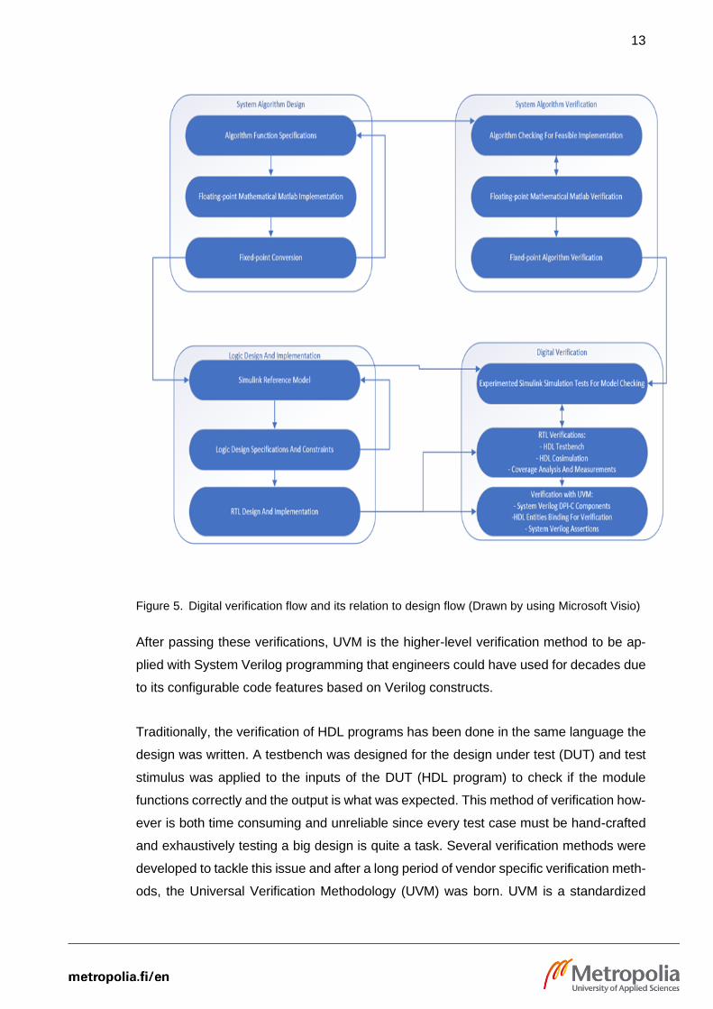
The verification flow applied for the Thesis project is shown in figure 5. At the initial de-
sign stage, design specifications are considered with a verification plan for feasibility.
After this period, verifications are implemented to guarantee the module functional char-
acteristics to be expected. That is, floating-point code and fixed-point mathematical code
are used to verify the module functional characteristics. If any design error occurs during
simulation, there would be an inevitable change on algorithm specifications. Simulink
modeling is used to be as a reference algorithm due to its characteristics for visualization
and sample-based simulation. That is, the design dataflow can be observed sample by
sample during the simulation for fast error checking and easy debugging ability to inter-
vene and adjust block properties to achieve model functional correctness. Configured
diagnostics for the Simulink reference model are observed after simulation experiments
to check model functionalities. In addition, Simulink components of each subsystem are
utilized to be converted to DPI-C reference mathematic coding which is run under UVM
test environment through Direct Programming Interface to generate the reference input
stimuli and expected output data. These stimuli are driven into RTL DUT and RTL cap-
tured output will be in comparison with the available expected output from DPI-C coding
parallel simulation. For RTL verification, HDL testbench is coded to verify RTL design in
the specific use case to meet the functional specifications. Logic simulation is applied by
utilizing this testbench. Later, to debug whether there is any design misoperation which
differentiates RTL design from the reference model or not, HDL Cosimulation is used to
set up mutual connections between Simulink and HDL Simulator. The identical stimuli
are applied to both Simulink reference model and RTL DUT for parallel simulation then
their outputs are captured to be compared with design goal which is to achieve the bit-
to-bit zero difference.
13
Figure 5. Digital verification flow and its relation to design flow (Drawn by using Microsoft Visio)
After passing these verifications, UVM is the higher-level verification method to be ap-
plied with System Verilog programming that engineers could have used for decades due
to its configurable code features based on Verilog constructs.
Traditionally, the verification of HDL programs has been done in the same language the
design was written. A testbench was designed for the design under test (DUT) and test
stimulus was applied to the inputs of the DUT (HDL program) to check if the module
functions correctly and the output is what was expected. This method of verification how-
ever is both time consuming and unreliable since every test case must be hand-crafted
and exhaustively testing a big design is quite a task. Several verification methods were
developed to tackle this issue and after a long period of vendor specific verification meth-
ods, the Universal Verification Methodology (UVM) was born. UVM is a standardized
14
methodology now supported by all the major simulator vendors. The UVM class library
brings a lot of automation to the SystemVerilog language such as sequences, data au-
tomation features and macros. With UVM it is possible to create reusable, automated
and adaptable test environments that accelerate the verification of complex hardware
designs and make it possible to achieve much better test coverage with reduced effort
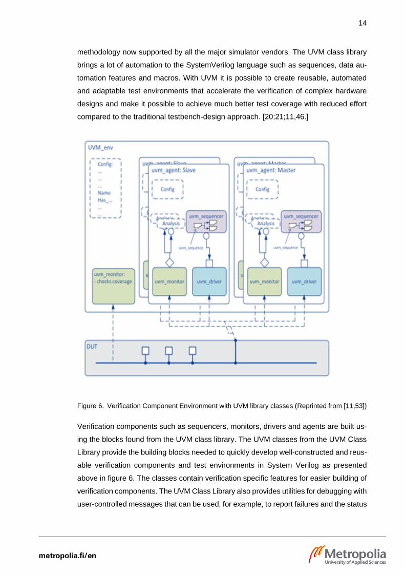
compared to the traditional testbench-design approach. [20;21;11,46.]
Figure 6. Verification Component Environment with UVM library classes (Reprinted from [11,53])
Verification components such as sequencers, monitors, drivers and agents are built us-
ing the blocks found from the UVM class library. The UVM classes from the UVM Class
Library provide the building blocks needed to quickly develop well-constructed and reus-
able verification components and test environments in System Verilog as presented
above in figure 6. The classes contain verification specific features for easier building of
verification components. The UVM Class Library also provides utilities for debugging with
user-controlled messages that can be used, for example, to report failures and the status

15
of every test operation on any level of the testbench, even globally. To be more precise,
the UVM classes and utilities are divided into categories pertaining to the specific roles
or functions such as UVM core base class, reporting classes provide a facility for issuing
reports with consistent formatting and configurable side effects based on design verbos-
ity and severity, factory overrides to manufacture UVM objects and components, phasing
capability, configuration database, type parameterized data structures, and UVM reusa-
ble and configurable verification components. [21;11,53.]
Below are the main UVM verification components [11,53-54] explained briefly:
• Data item: Any input to the DUT network packets, buses, transactions or protocol values
and attributes.
• Driver: Emulates the logic driving the DUT. Accepts data input which it can sample and
feed to DUT.
• Sequencer: Stimulus generator that feeds the driver.
• Monitor: A passive entity that samples DUT signals. Monitors collect coverage infor-
mation and perform the checking of the data.
• Agent: An agent encapsulates drivers, monitors and sequencers to simplify the usage
of verification components by providing an abstract container which can perform a com-
plex task without independently configuring every component.
• Environment: Top-level component of verification components and agents has the con-
figuration properties for customization and re-use of the whole component topology with-
out altering the internal components.

16
Figure 7. The UVM Phases (Reprinted from [17,11])
The UVM uses phases which are described in detail in figure 7. It allows a consistent
testbench execution flow during simulation. There are three different groups of phases
executed in the following order [17,11.]:
• Build phases: where the testbench is configured and constructed.
• Run-Time phases: where time is consumed in running the testcase.
• Clean-up phases: where the results of the testcase are collected and reported.

17
4 Design Specifications and Algorithm to Architecture
The Adaptive FIR Filtering Noise Cancellation module updates the filter weights based
on LMS algorithm as FIR filtering procedure. The original input signal source is a com-
plex-valued sinusoidal signal which is stimulated with configured length. The noise
source is randomly generated then being filtered by FIR filtering process to create the
corrupted noise. After the addition of the original input and the corrupted noise, the result
of this procedure is the desired signal source which will be scaled for fixed-point imple-
mentation.
Before adaptive FIR filtering implementation, through configured tests, adaptation step
size is selected to optimize the adaptive filtering process.
The tapped delay noise input and the estimation error output after each adaptive filtering
procedure are used to calculate the updated filter weights based on adaptation step size.
4.1 LMS Algorithm for Digital Design and Implementation
Based on the diagram as in figure 8, LMS algorithm consists of two basic processes that
continually build mutually:
• Filtering process: filter output computation includes FIR filter design of noise input
based on updated weights to get the calculated filtered signal and the subtraction of this
filtered signal from the desired input signal to obtain the estimation error output.
• Adaptation process consists of weight update logic, tapped delay input processing,
weight update controller.

18
Figure 8. Signal-flow graph representation of the LMS algorithm (Reprinted from [1,267])
The specified architecture is required to perform a design bit-level architecture for vector-
vector multiplication used for output calculation with finite convolution sum applied algo-
rithm.
Figure 9. Detailed RTL architecture of LMS algorithm (Drawn by using Microsoft Visio)

19
A detailed top-level module architecture is demonstrated in figure 9. It contains two par-
tial designs: filter weights adaptation and filter output computation. The left-side design
describes how the filter coefficients adapt to the optimal solution. For each valid clock
cycle, the delayed input is generated from Tapped Delay core. The estimation error reg-
ister will multiply by the fixed step size parameter, then the result will go through trunca-
tion, round and wrap procedures respectively. This result called adaptive correction will
continue to multiply by the delayed input before rounding and wrapping to get the needed
offset for weights adaptation. The addition between the weight offset and the weight reg-
ister is to update to create a new set of filter coefficients. Meanwhile, filtering process is
parallelly operated, which can be seen in detail at the right side of the figure 9. It de-
scribes the filter output computation. To be more specific, for each valid clock cycle, there
occurs the multiplication between the generated set of filter weights and the delayed
input to result in the output array with its size as the filter length order. After round and
wrap, cumulative sum of elements and resize procedures, the final filtered output is used
for subtraction operation based on noise cancellation algorithm to obtain the estimation
error register. The Q-format [10,530] to be shown for each signal are configured in ad-
vance, is 1.24.23 that it means the signal is represented in signed binary format, 24 is
the word length and 23 is the fractional length. In summary, these two design processes
operate simultaneously and have a mutual impact on each other.
Figure 10. Tap delay processing of RTL Tapped Delay core (Drawn by using Microsoft Visio)
The Tapped Delay core for the adaptive noise cancellation module is shown in figure 10.
In the tap processing, each tap is controlled by the valid clock signal. The input from
each tap is shifted and stored to be combined with the next tap input after one-cycle
delay operation. The reference noise input is propagated through all taps and automati-
cally replaced by shift arithmetic process. [27.]

20
Figure 11. Weight update control mechanism for RTL (Drawn by using Microsoft Visio)
Weight update control mechanism is shown in figure 11. For every rising edge of the
clock signal, the weight update process evaluates the valid signal which enables the
register operation for signals to be used for mathematical computations.
4.2 Design Configurations and Constraints
The LMS algorithm designed for adaptive FIR filtering noise cancellation module is com-
plex in the sense that the input and output data as well as the tap weights are all complex
valued.
To be more specific, Matlab implementation, floating-point to fixed-point conversion, cod-
ing style and verification functional requirements are the considered aspects at the early
design period to specify detailed variable parameters for design compatibility as well as
its configurability.
4.2.1 Floating-point Matlab Implementation
Relevant parameters related to adaptive LMS FIR filtering algorithm is configured as
below:
• FIR filter length is 45, which is not only sufficient for coefficient adaptation but also an
effective tap order number for FIR filtering.
• Stimulus length is 1000, which is high enough to allow an effective design functional
characteristics observation.

21
• Scale Factor Adjustment: It is acceptable for accuracy limitation when transitioning from
a floating point to a fixed‐point representation. The conversion method is to keep a limited
number of decimal digits. Normally, two to three decimal places method is appropriate
for digital filter processing. Therefore, the scale factor can easily be obtained by multi-
plying the data values by 100 and divide the calculated values by 100 to recover the
anticipated value. [13,24-25.] For complex signal, the common scale factor is the maxi-
mum value between the calculated scale factor of real part and the another one of imag-
inary part to guarantee that the output values are in the interval [-1, 1].
• Clean original input signals is a complex-valued sinusoidal signal which includes in
dependent sinewave sequences containing the sine of elements over the domain which
ranges are proportional to (−π,π) with multiplying constants of 5 and 6 respectively. Their
step-incremental values are also in the interval [-1, 1] with a determined range which is
corresponding to the configured stimulus length. Therefore, signal resolution is about
6.23*10^^-3 (radians).
• The noise input is generated as a random Gaussian noise sequence to be scaled by
dividing by the common scale factor. The correlated noise input is generated by using a
22-th order window-based FIR bandpass filter with passband 0.35π≤ω≤0.65π rad/sam-
ple. The desired input is an addition of the clean sinewave input and the correlated noise
input after being scaled by dividing by the common scale factor.
• The necessary condition for the step size parameter u to satisfy the convergence time
constant is 0 < u << 1 [3,296]. In addition, if u is made too large then the algorithm
becomes unstable. Therefore, u is determined to be optimal by test experiments using
Matlab coding with pre-defined conditions.
4.2.2 Floating-point to Fixed-point Conversion
Floating point circuits have higher power consumption and lower performance compared
to fixed point. For the vast majority of DSP applications, fixed point arithmetic is suitable,
especially FIR filtering algorithm. [9,545-546.] For fixed-point conversion, signal dynamic
range is mapped into the limited fixed-point precision [2,366].
Using finite word lengths prevents us from representing values with infinite precision,
inaccurate arithmetic results. The level of output roundoff noise in fixed-point implemen-
tations can be reduced by increasing the word length. [5,647.]

22
The value bit width of 24 is chosen to be configured for quantization process due to its
step resolution of 1/8388608 which works out to 1.192 * 10-7, leads to the significant
reduction of error percent of signal level. To perform mathematic computations in RTL
design, Q1.23 format to represent signed values with fraction bits of 23 is used.
The next finite word-length effect to be considered is data overflow. Round and wrap on
overflow are the chosen method due to hardware resource accuracy minimization, es-
pecially suitable for configured bit-level design. For addition and multiplication processes
in RTL coding, the results are always truncated to Q1.23 format to meet the data bit width
requirements as configured before.
4.2.3 Coding Style
MATLAB is generally used for algorithm design of a system for fast simulation and veri-
fication purposes of the behavioral model. To produce rational HDL code, the algorithm
should be written from the hardware perspective. Algorithm models are often written into
simulation optimized vector operations that create parallel structures and copies of com-
binational logic blocks in hardware. To create synthesizable MATLAB code, the structure
must be correct. Register modeling is done through “persistent” variables. The variables
that are wanted to save their states are defined in MATLAB function as persistent and
these variables generate registers into RTL. [12,21-23.]
Figure 12. Gated clock method to reduce power consumption (Reprinted from [22,12])

23
RTL implementation uses gated clock method as described in detail in figure 12 is utilized
to reduce power consumption in device architectures by effectively shutting down por-
tions of a digital circuit when not being in use [22,12].
4.2.4 Verification Requirements
All-passed verification from simulation-based verification with HDL testbench, bit-accu-
rate parallel verifications with HDL Cosimulation and most importantly, UVM testbench
that use constrained stimulus generation and functional coverage methodologies is the
must-meet design goal. Apart from modular and reusable coding style, specifically for
the mathematical algorithm, Matlab implemented coding is re-quired to be in separate
functions which are targeted to a dynamic system.
In addition, the structural coverage analysis with code coverage result of 100% along
with all concurrent System Verilog assertions evaluated to be passed are the fundamen-
tal factors to clearly demonstrate design functional correctness.

24
5 Adaptive FIR Filtering Noise Cancellation Module Implementation
5.1 Matlab Analysis and Implementation
5.1.1 Floating-point Matlab Implementation
When the LMS algorithm is operating in a limited-precision environment, the point to note
is that the step size parameter may be decreased only to a level at which the degrading
impacts of round-off noises in the tap weights of the finite-precision LMS algorithm be-
come significant [1,515].
In addition, as mentioned in section 4.2.1, step size that is too small increases the time
for filter convergence or that is too large may cause the adaptive filter to diverge [27].
Therefore, to be in compliance with the step size condition, the step size u must be 0 <
u << 1.
Listing 1. Matlab implementation for adaptation step size test selection
As seen in listing 1, the design configurations are fixed as specified in section 4.2.1 for
input signals, the pre-defined filter length of 45 taps and the stimulus length of 1000. The
available Matlab supported system object dsp.LMSFilter is utilized to compute estimation
error output of the adaptive LMS filter according to the step size parameter which is
experimentally determined. XY plot is used to show the output signals over time.
In figure 13, the blue signal is the clean original sinusoidal wave which runs at the same
time with the filtered output signal which is the red one. The optimal solution is reached
when the error difference between these two signals is at the minimum value. Therefore,

25
after test experiments with gradual reduction of step size parameter, 0.008 is the best
choice because it is small enough but efficient to meet the design requirements to get
the optimal convergence.
Figure 13. MATLAB GUI displaying the result of step size test selection after simulation
After defining the fixed adaptation step size, other design specifications must be config-
ured independently as shown in listing 2. That means it is easy and convenient to modify
if there is any change from the design algorithm. Matlab top-level design and Simulink
reference model import this configuration as a design callback.
Listing 2. Matlab function for initial design configurations

26
The detailed declaration for reference inputs of the Matlab mathematical testbench are
shown in listing 3. These input declarations are to follow the design specification speci-
fied in section 4.2.1. The two inputs, which are the reference noise and the desired sig-
nal, are both generated in the sense of complex values. Moreover, window-based FIR
filter design with the usage of dsp.FIRFilter system object is to generate correlated noise
from original noise input. It uses a Hamming window to design a 22-th order FIR band-
pass filter with passband 0.35π≤ω≤0.65π rad/sample. The correlated input will be added
to the clean sinewave to form the desired signal. Obviously, the scaling method is applied
for original noise input and desired signal to adjust their value ranges to be in the interval
[-1, 1].
Listing 3. Input declarations for adaptive FIR filtering noise cancellation testbench
Down to the verification of the Matlab testbench as can be observed in listing 4, it calls
the main implementation of adaptive LMS FIR filtering noise cancellation for separate
data paths. Because both of two inputs are complex-valued format, to implement the
adaptive LMS algorithm, their data paths are divided into real path and imaginary path.
Each data path is independent to implement the adaptation process before complex-
valued combination only at the final stage to get the final outputs. Therefore, there are
two separate comparison plots for each data path.

27
Listing 4. Call to the main design implementation from Matlab testbench and graphical plots of outputs after test simulation
The design goal is to implement design code to be configurable and reusable that there
are modular functions coded for partial designs. Besides, to register the filter coefficients
for Matlab mathematical algorithm, persistent variable declaration is used as can be seen
in listing 5.
Listing 5. Persistent variable usage for RTL description of filter weights
Adaptive LMS FIR filtering noise cancellation implementation is mainly divided into three
modular functions to be shown in detail in listing 6, listing 7 and listing 8. These functions
aim to be the design callbacks when the top-level design call them to perform FIR filtering
and weight update process before output computation at the end of each step adaptation.

28
Listing 6. Tapped delay Matlab function
As seen in listing 6 above, the noise reference input is delayed at each simulation step
to form 45 taps which is previously defined as exactly equal to the filter coefficient length.
The persistent variable u_d is responsible to store the tap input which is in vector form
for shifting process when the top-level design calls the tapped delay function.
Listing 7. Weight update logic Matlab function

29
The main adaptation procedure is described in listing 7. The weight update logic is im-
plemented step-by-step in a clear coding style, follows the LMS reference algo-rithm.
The Matlab code is to use reset_weights variable and update_weights variable to set the
weight update control mechanism.
Listing 8. Cumulative sum of elements Matlab function
FIR Filtering process is simply described in listing 9. To be more specific, after vector-
vector multiplication between tapped delay input and the filter coefficient set, cumulative
sum of elements procedure shown in detail in listing 8 is implemented to calculate the
filtered signal based on the computed filter weights as the input variable.
Listing 9. Filtered output computation procedure from Matlab reference design
After design steps of Matlab mathematical algorithm mentioned previously, the Matlab
testbench is run to verify adaptive FIR filtering noise cancellation reference design. The
plot of outputs for each data path is shown in figure 14.

30
Figure 14. Graphical plot to show Matlab testbench outputs after simulation
The adaptive FIR filtering noise cancellation is successfully operated. The desired signal
is the addition of the clean sinewave stimulus and the noise reference input. To be com-
pared with the desired signal, the estimation error signal reached the cleaner version
due to noise elimination. To be more precise, the estimation error is the result of the
subtraction the FIR-filtering filtered output signal from the desired signal.
5.1.2 Fixed-point Matlab Mathematical Testbench
To implement floating-point to fixed-point conversion, fixed-point mathematics configu-
ration is simply specified in Listing 10 below which is added to every Matlab floating-point
code.
Listing 10. Matlab fixed-point mathematics configuration
As listing 10 demonstrated, step_v is exceptional to be configure only for fixed-point step
size while dat is configured for remaining signals.
31
5.2 Simulink Reference Modelling
Simulink is a graphical design tool that uses library blocks, MATLAB functions and Sys-
tem Objects to perform indicated tasks and functions. Simulink library contains huge se-
lection of hardware optimized blocks. These blocks are divided into different categories
to be integrated in SoC development. User-defined MATLAB function blocks and System
Object blocks can be used to self-define design specific configurations or to reutilize
available MATLAB mathematical computations. The blocks are built in Simulink model-
ing by referring the Matlab reference algorithm with fixed-point data types. A test bench
in Simulink is built by driving all input variables into Device Under Test and capturing
DUT outputs to be verified. The data is imported as streaming data with generic param-
eter configurations. [12,24-25.]
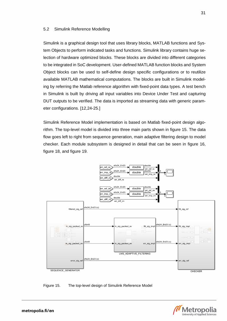
Simulink Reference Model implementation is based on Matlab fixed-point design algo-
rithm. The top-level model is divided into three main parts shown in figure 15. The data
flow goes left to right from sequence generation, main adaptive filtering design to model
checker. Each module subsystem is designed in detail that can be seen in figure 16,
figure 18, and figure 19.
Figure 15. The top-level design of Simulink Reference Model
32
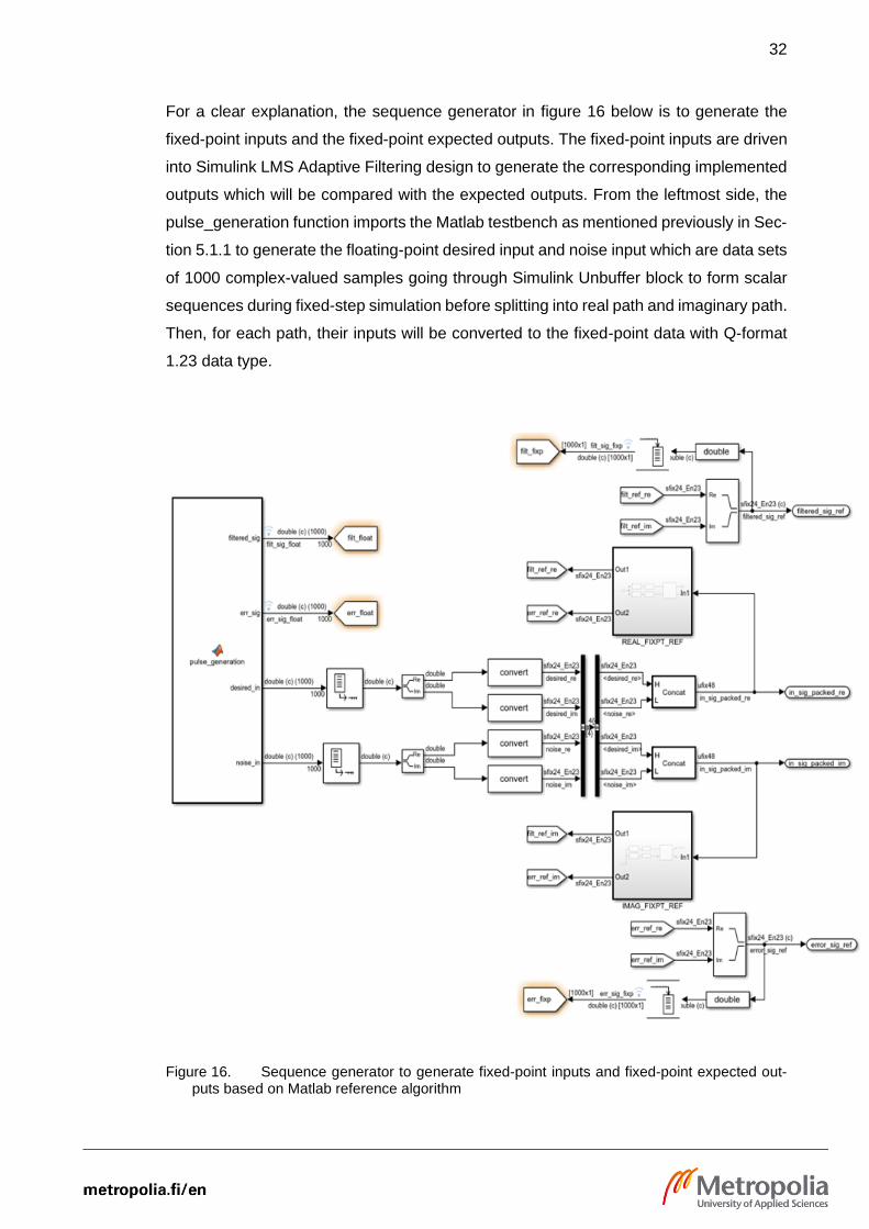
For a clear explanation, the sequence generator in figure 16 below is to generate the
fixed-point inputs and the fixed-point expected outputs. The fixed-point inputs are driven
into Simulink LMS Adaptive Filtering design to generate the corresponding implemented
outputs which will be compared with the expected outputs. From the leftmost side, the
pulse_generation function imports the Matlab testbench as mentioned previously in Sec-
tion 5.1.1 to generate the floating-point desired input and noise input which are data sets
of 1000 complex-valued samples going through Simulink Unbuffer block to form scalar
sequences during fixed-step simulation before splitting into real path and imaginary path.
Then, for each path, their inputs will be converted to the fixed-point data with Q-format
1.23 data type.
Figure 16. Sequence generator to generate fixed-point inputs and fixed-point expected out-puts based on Matlab reference algorithm
33
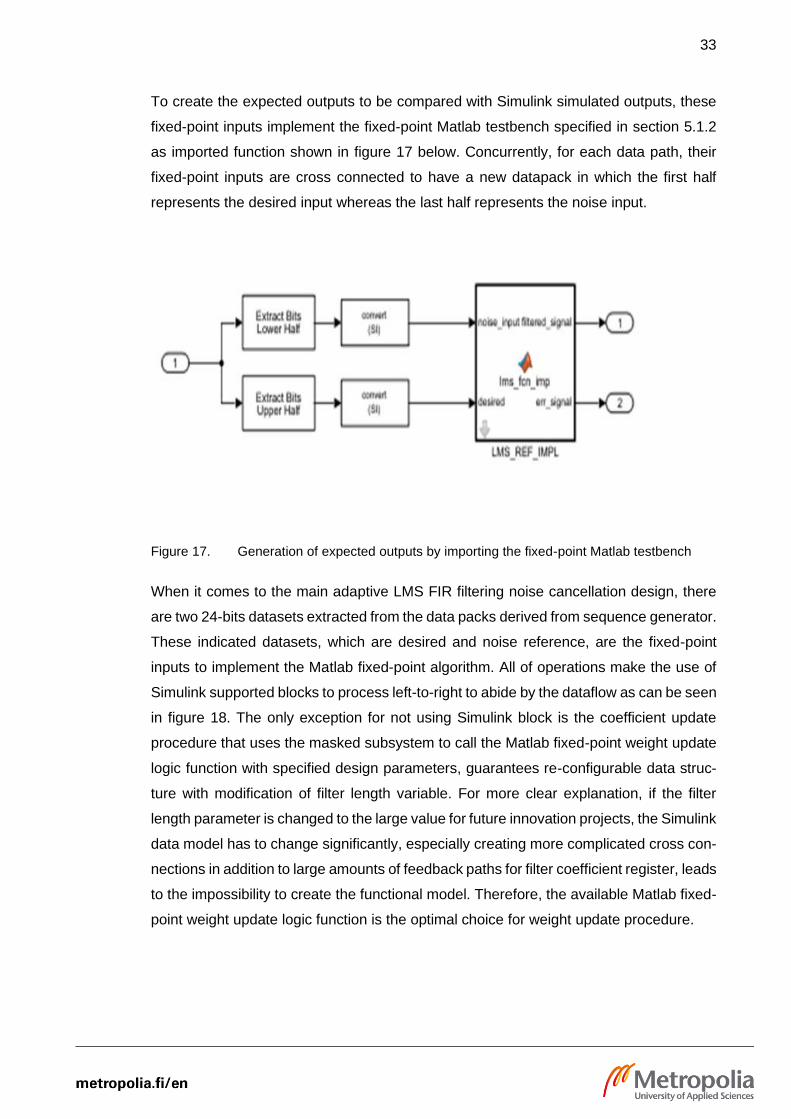
To create the expected outputs to be compared with Simulink simulated outputs, these
fixed-point inputs implement the fixed-point Matlab testbench specified in section 5.1.2
as imported function shown in figure 17 below. Concurrently, for each data path, their
fixed-point inputs are cross connected to have a new datapack in which the first half
represents the desired input whereas the last half represents the noise input.
Figure 17. Generation of expected outputs by importing the fixed-point Matlab testbench
When it comes to the main adaptive LMS FIR filtering noise cancellation design, there
are two 24-bits datasets extracted from the data packs derived from sequence generator.
These indicated datasets, which are desired and noise reference, are the fixed-point
inputs to implement the Matlab fixed-point algorithm. All of operations make the use of
Simulink supported blocks to process left-to-right to abide by the dataflow as can be seen
in figure 18. The only exception for not using Simulink block is the coefficient update
procedure that uses the masked subsystem to call the Matlab fixed-point weight update
logic function with specified design parameters, guarantees re-configurable data struc-
ture with modification of filter length variable. For more clear explanation, if the filter
length parameter is changed to the large value for future innovation projects, the Simulink
data model has to change significantly, especially creating more complicated cross con-
nections in addition to large amounts of feedback paths for filter coefficient register, leads
to the impossibility to create the functional model. Therefore, the available Matlab fixed-
point weight update logic function is the optimal choice for weight update procedure.

34
Figure 18. Simulink LMS design to implement adaptive noise cancellation process
After adaptive noise cancellation implementation, to verify model functional correct-
ness, the checker shown in figure 19 verifies the equivalence checking between the
golden reference output derived from fixed-point Matlab testbench implementation and
the another one achieved from Simulink simulation.

35
Figure 19. The checker to compare the implemented outputs with the expected outputs
This checker imports the Matlab lms_checker function demonstrated in listing 11 for the
response checking of both filtered output and estimation error output. This function eval-
uates the size difference of the two inputs for dimensional comparability. The test result
must be passed to move onto the next verification that compares the expected signal
with the implemented signal for every corresponding element. The assertion messages
will be displayed for compatible test cases during Simulink simulation.

36
Listing 11. Checker function to verify signal equivalence checking
The final step to verify is to run the Simulink reference model. For detailed waveform
analysis of the output signals which can be observed in figure 20, the blue signal is the
sinusoidal wave of estimation error signal whereas the red line indicates the error differ-
ence of zero which is calculated by subtracting the Simulink implemented data from the
Matlab reference data.

37
Figure 20. Graphical plot to show estimation error output and the zero difference between Matlab reference data and Simulink implemented data
In addition, the messages from lms_checker function for test-passed verification are on
the Diagnostic Viewer display during Simulink simulation.
Figure 21. Diagnostic viewer of checker function during Simulink simulation
As figure 21 illustrated, the messages mean the Simulink reference model is designed
as exactly specified as Matlab reference mathematical algorithm.

38
5.3 Register Transfer Level Design with VHDL
The final design phase is to create Register Transfer Level descriptions of the Simulink
attributes. The RTL designs are required to have integrated HDL coding style to validate
the Simulink reference model.
All RTL implementations are coded in VHDL according to design specifications and con-
straints mentioned in chapter 4. To be more specific, fixed predefined design parameters
are configured in LMS_ADAPTIVE_FILTERING_pkg.vhd file as illustrated in listing 12.
Apart from initial declarations of fixed parameters such as filter coefficient length and
weight update control logics, the constant w_data_c of 24 is the common data word
length configuration for all data signals which are design entity in-puts, entity outputs and
the outputs of different binary arithmetic operations. Besides, w_mult_c of 48 and w_ad-
der_c of 30 are the constants used for multiplication and finite convolution sum. Further-
more, data word length of step size is to obey the specified design specification that its
fractional length is 30 and its word length is 24. In addition, it is fixed to be an unsigned
binary of 0.008 which hexadecimal converted result is 83126F.
Listing 12. Data declarations of fixed parameters in HDL package file
As specified in section 4.2.2 about overflow handling and rounding, round and wrap on
overflow is the chosen method to be coded as an HDL procedure that can be seen in
listing 13. Its inputs are based on the following factors: rounding Most Significant Bit,
rounding Least Significant Bit and wrapping Most Significant Bit. There are two concur-
rent procedures that the rounding procedure uses resize function to truncate input to

39
data with a new specified data width but retain the sign bit as can be seen in line 75
whereas the wrapping procedure is going through recursive OR operations with the us-
age of for loop as coded from line 80 to line 82 before using different bitwise calculations
based on the wrapping theory to generate the wrap bit. The result from rounding and
wrapping procedures is the addition of the rounded variable and the wrap bit. More-over,
the cumulative sum of elements procedure is also directly coded at the top of the identical
HDL package file as can be seen from line 45 to line 61.
Listing 13. HDL procedures for overflow handling and cumulative sum computation
The main RTL coding for adaptive noise cancellation algorithm is separated into three
partial operations which run simultaneously. RTL coding style uses rising clock edge to
drive the signal logic and asynchronous reset which will be activated when the reset
signal is asserted. To be more explicit, tapped delay processing described in listing 14
is to generate 45-taps noise reference input.

40
Listing 14. HDL procedure to create tapped delay signal from noise input
In addition, as can be seen in listing 15, adaptive weight update from line 90 to line 99 is
to utilize mathematical computations based on adaptive LMS FIR filtering theory. For
every clock cycle, valid signal starts filter coefficient registering.

41
Listing 15. RTL top-down adaptation process
As coded from line 112 to line 117 in listing 15, FIR filtering of the delayed noise input
according to the updated filter coefficient set and the tap delay of noise reference is the
vector-vector multiplication to create a new set of filter weights which then goes through
the rounding and wrapping procedure. After that, the adaptive filtered output is generated
by using cusum procedure declared in HDL package file for finite summation of the cal-
culated filter weight.
42
6 Adaptive FIR Filtering Noise Cancellation Module Verification
The verification techniques used to verify RTL design of Adaptive FIR Filtering Noise
Cancellation module are explained here and the results of these verifications are also
presented. RTL design in this Thesis goes through multiple levels of verification. Queta-
Sim as an HDL Simulator empirically checks simulation-based RTL functional character-
istics with assertions and provides the design code coverage analysis. Besides, HDL
Cosimulation establishes mutual connections between Simulink and QuestaSim for par-
allel simulations to guarantee that RTL design does what Simulink reference modeling
expects under clock synchronization condition. Finally, an UVM based bit-exact simula-
tion testbench is used to verify the specific use case. The HDL entities are integrated to
the UVM environment. The DPI-C mathematical model, which is converted from the Sim-
ulink reference model, is to run to generate input stimulus and the reference output data.
During UVM test simulation, the generated input stimulus will stimulate RTL entities then
their output data will be captured to be compared with the DPI-C generated reference
output data.
6.1 HDL Testbench Generation and Simulation with Questa Sim
This first verification to verify RTL design is to generate a HDL test bench to simulate
HDL design files in QuestaSim simulator.
This test bench verifies the created HDL DUT against test vectors generated from Sim-
ulink reference model. The input stimulus and expected data, which are generated from
Simulink simulation, are stored in data files (.dat). In detail, the input data are
in_sig_packed_re, in_sig_packed_im and the output data are err_sig_impl_re_expected,
err_sig_impl_im_expected, filt_sig_impl_re_expected, filt_sig_impl_im_expected that
their data format is hexadecimal number. During HDL simulation, the HDL test bench will
read the input stimulus derived from the input data files then drive these stimuli to DUT
input ports as illustrated in listing 16. After that, the HDL testbench captures the actual
DUT outputs which will be compared with the corresponding expected outputs stored in
the output data files.

43
Listing 16. RTL entities binding to the HDL testbench
As can be seen in listing 17, for real data path, the process statement describes the
procedure which opens in_sig_packed_re.dat file to read the input stimulus as read_data
variable then stores it as a raw data for the registering process. Because stimulus cap-
ture is dependent on not only system clock signal but also intrinsic rdEnb variable value,
there are two concurrent processes that the first one as coded from line 259 to line 266
is responsible to hold raw data at every rising clock edge to be driven into offset data if
sequence reading is disabled, whereas the remaining one as coded from line 268 to line
275 is to immediately achieve raw data as an offset data if there occurs any change of
raw data.
Listing 17. Sequence generation to drive stimulus to the HDL Design Under Test

44
The HDL testbench is configured that it opens the reference data .dat file then reads the
captured data as expected outputs. After that, the expected outputs will be compared
with RTL implemented outputs. As a sample demonstration, the verification of real-val-
ued filtered output is shown in listing 18. Expected filtered output reading procedure is
coded from line 374 to line 388 and the equivalence checking process is coded from line
390 to line 402 in which at every valid rising clock edge, there is an assertion to verify
whether the actual RTL output is equal to the expected output or not.
Listing 18. HDL equivalence checking of actual RTL output and Simulink expected output

45
After HDL compilation, QuestaSim is used to run the configure HDL testbench to verify
the functional correctness of RTL design. The detailed waveform shown in figure 22 is
that the test result is passed after a completed simulation.
Figure 22. Detailed waveform of signals from HDL testbench verification by QuestaSim
For an instance explanation, observing at 199120 ns, all RTL implemented outputs are
equivalence to the respective reference outputs and their asserted variables for test fail-
ure checking are always zero during test simulation.
6.2 Code Coverage
Code coverage is a technique to collect the statistics on the execution of each line of
HDL code. Its coverage analysis is evaluated using the built-in features of QuestaSim to
measures how many times certain aspects of the source are exercised while running a
suite of tests. Code Coverage types are divided into Statements, Branches, FEC Ex-
pressions, FEC Conditions, Finite State Machine and Toggles. [16,41-48].

46
Figure 23. Code coverage result of the main HDL coding of the design module
For RTL design of Adaptive LMS FIR Filtering Noise Cancellation module, there are only
Statements, Branches and Toggle coverages needed for statistics analysis. The
achieved results are shown in figure 23 and figure 24.
Figure 24. Code coverage result of HDL coding of design package file
For both real path and imaginary path, code coverage reached 100% as the desired goal
mentioned in section 4.2.4. Therefore, the verification for code coverage of RTL design
was considered done.

47
6.3 HDL Cosimulation Verification
Co-simulation automatically drives stimulus into an HDL model from Simulink testbench
and runs a RTL simulator concurrently. Cosimulation compares expected output derived
from Simulink testbench to the HDL model’s output. HDL Verifier is required to be in-
stalled. Co-simulation compares the models bit-accurately and cycle-accurately. [12,32.]
Simulink configuration is presented in figure 25 below.
Figure 25. HDL Co-simulation configuration (Reprinted from [12,32])
Mathworks reference documentation [23] briefly described the procedure of how to set
up a communication link between Simulink and HDL simulator through HDL Cosimula-
tion, stating that:
In co-simulation, it creates a communication link between the HDL simulator and Simulink. Such a link enables to verify a model directly against the HDL implemen-tation, create test signals and testbench for HDL code, use a behavioral model as a reference in an HDL simulation, use analysis and visualization features for real-time insight into an HDL implementation, integrate a new model with the existing HDL design. [23.]
Error is calculated from the differences of Simulink model simulation and RTL simulation.
Start time alignment is configured for delay balancing between Simulink and RTL simu-
lator. If RTL is written correctly to perform functional characteristics of Simulink model,
then the error should be zero. The comparison is done on the output ports and it is a
rapid method to verify HDL design correctness every time the reference algorithm is ad-
justed. [12,32.]

48
Figure 26. Simulink cosimulation model of adaptive FIR filtering noise cancellation
To be more specific, the Simulink reference model that includes an HDL Cosimulation
block shown in figure 26 above will run the generated HDL code in QuestaSim HDL
simulator. This block drives Simulink stimulus into RTL input ports of DUT then captures
the actual outputs from DUT to compare against Simulink reference outputs of
LMS_ADAPTIVE_FILTERING subsystem.

49
Figure 27. The comparison plot to show Simulink estimation error output and its RTL output
The plot presented in figure 27 is to prove the correctness of RTL design against Simulink
mathematical model. The topmost sinusoidal wave is the achieved estimation error out-
put derived from DUT meanwhile the middle one represents its Simulink simulated out-
put. As can be seen, these sinusoidal waves have the identical characteristics. The bot-
tom line is the error difference being zero over time simulation between DUT output and
Simulink reference output. Therefore, the design functional characteristics are correctly
converted from Simulink modeling to RTL design coding.
6.4 Functional Verification with Universal Verification Methodology
For this Thesis project, Direct Programming Interface was utilized to create a UVM test
environment. This environment contains a System Verilog DPI top module which is bind-
ing to RTL design under verification. The UVM test bench basically includes a sequence,
a scoreboard, and design under verification. As demonstrated in figure 28, the top mod-
ule which comprises clock and reset signals to control system process, instantiates De-
sign Under Verification (DUV) which is connected to verification environment through
module interface. The UVM environment consists of the scoreboard and the agent which
includes a sequencer, a monitor and a driver. The detailed process of UVM testbench is
that the sequence object which defines a set of transactions, is divided into two paths.
For the first path, the sequencer is responsible for routing the stimulus data from the
sequence to the driver which will transform each transaction to the desired protocol and
drives the transaction to the DUV through the virtual interface. After RTL operations of
DUV, the passive UVM monitor samples implemented output data to send to the score-
board. The remaining path is a direct path in which the scoreboard receives the reference

50
output data from the sequence object then compares this expected data with the imple-
ment data from RTL DUV.
Figure 28. UVM Testbench Architecture (Reprinted from [25])
To be more precise, Simulink subsystems are exported as generated C codes which
describe design implementations to be integrated with UVM environment with a direct
programming interface (DPI). It means that UVM sequence, DUV, and UVM scoreboard
are generated from Sequence Generator, LMS Adaptive Filtering design and Checker
subsystem respectively. These DPI-C codes can be found at subsystem build directories
that there are subsystem DPI package files for function declarations, the generated Sys-
tem Verilog DPI subsystem, and the DPI-C subsystem wrappers for C descriptions of
Simulink design operations.

51
UVM hierarchy configuration is briefly demonstrated in lms_pkg.sv file as can be seen in
figure 29.
Figure 29. UVM Hierarchy as presented in HDL package file
The functionalities of UVM artifacts as presented in figure 29 are defined below:
• mw_LMS_FILTERING_sequence_trans.sv – This file includes type definitions of se-
quence items
• mw_LMS_FILTERING_sequence.sv – This file contains sequence declarations and
sequencer instantiation.
• mw_LMS_FILTERING_trans.sv - This file contains a UVM object that defines the input
transaction type for the scoreboard.
• mw_LMS_FILTERING_driver.sv - This file includes a pass-through UVM driver by de-
fault.
• mw_LMS_FILTERING_monitor.sv - This file includes a UVM monitor. The monitor sam-
ples implemented signals from the DUV to the scoreboard.
• mw_LMS_FILTERING_monitor_input.sv - This file includes a pass-through UVM mon-
itor. The monitor samples expected signals from the driver to the scoreboard.

52
• mw_LMS_FILTERING_agent.sv - This file includes a UVM agent that instantiates se-
quence, driver, and monitor.
• mw_LMS_FILTERING_scoreboard.sv – This file consists of a UVM scoreboard
• mw_LMS_FILTERING_environment.sv - This file includes a UVM environment, that
instantiates an agent and a scoreboard.
• mw_LMS_FILTERING_test.sv - This file includes a UVM test which is based on the
specified use case of adaptive LMS filtering design.
After completing UVM configurations, the System Verilog top design illustrated in listing
19 is integrated with UVM environment. The UVM interface as coded in mw_LMS_FIL-
TERING_if.sv file is to connect with DPI-C representation of Simulink LMS Adaptive Fil-
tering design subsystem. During UVM simulation, it receives stimulus from UVM driver
then drives them into the scoreboard through UVM monitor for UVM response checking.
In addition, the top design utilizes this interface to capture DPI-C implemented output
signals to be compared with RTL outputs which is delayed for signal compatibility. The
RTL binding can be seen from line 43 to line 53.
Listing 19. Instantiations of UVM interface, RTL DUV, and Simulink DPI-C representation

53
The equivalence checking between real-valued RTL implemented estimation error and
its DPI-C representation is demonstrated in listing 20. The signal err_sig_impl_re_de-
layed is the delayed RTL estimation error output whereas err_sig_impl_re_ref is its Sys-
tem Verilog DPI-C generation. The equivalence checking is passed, leads to that
err_sig_impl_re_testFailure value is always zero.
Listing 20. Top-module equivalence checking in UVM environment written by System Verilog

54
The same coding technique is applied for filtered output at both real path and imaginary
path. If all of these checking are done without failure during UVM simulation then the
test-completed message is displayed, otherwise the test-failed message is shown in-
stead.
Figure 30. UVM testbench simulation with test-passed result
After HDL Design integration with UVM testbench, QuestaSim tool is used to verify UVM
simulation run. The result shown in figure 30 is to prove the previously specified equiva-
lence checking in addition to UVM test-passed simulation of 200030 ns.

55
Figure 31. Detailed waveform of inspected signals from UVM Testbench simulation
To analyze UVM test simulation in detail, the signal waveform as seen in figure 31 above
is to present all needed output signals over time. From a detailed observation at the
yellow cursor, for instance, at 199120 ns, err_sig_re_expt is Simulink DPI-C expected
estimation error captured from scoreboard that its value is equal to the value of
err_sig_impl_re which is RTL implemented estimation error. Their identical value under
hexadecimal format is 16E049, although their data bit width is different. The same results
are obtained for filtered output at both data paths.
6.5 System Verilog Assertions
An assertion is a statement about a design’s intended behavior which must be verified.
It is used to validate the behavior of the system defined as properties which are design
behavioral attributes. Its sole purpose is to ensure consistency between the designer’s
intention, and what is created. [15,3-4.]
For this Thesis project, System Verilog assertions were used to verify the correct func-
tionality of signal logic under valid control. Simple tests written were to check that tap
delay processing and weight update logic worked as expected. The register interface
writes the configuration and exports the data from the module internal registers to the

56
top-level configuration and data registers [11,80]. This connectivity from RTL design
module to top level registers to be coded as System Verilog assertions binding shown in
listing 21 below is to read RTL implemented output data then drive them into assertion
properties through the binding interface. Concurrent assertions are used at each rising
edge of the valid system clock to evaluate the behavior of RTL signal logic.
Listing 21. HDL entities binding to System Verilog assertion properties
To implement modular System Verilog assertions, the coding style used splits assertion
declarations into two parts as can be seen in listing 22. Sequence expressions are to
configure the functional tests for equivalence checking under control logic whereas prop-
erties are to specify the trigger conditions of the previous configured sequence expres-
sions. To be more specific, from line 21 to line 25, it means when valid_in is activated,
weights_sig value assigns to weight_v which will be stored as a temporary variable. At
the one next clock cycle, this variable will be compared to fil-ter_coeff_sig_1 which is the
weight update logic. The similar configuration applied to tap delay processing as can be
seen from line 27 to line 30 that there is a variable assignment from noise_signed to the
intermediate variable noise_in_v which will be in comparison with the shifted element of
tap delay register after one delayed clock cycle. For property declarations, from line 33
to line 47, it describes that at each rising edge of system clock, when valid_in triggers,
previous configured sequence expressions will be verified.

57
Listing 22. Sequence and property declarations for SystemVerilog concurrent assertions
In listing 23, from line 50 to line 62, there are assertions to verify the design properties
that if the asserted logic behaviors are not as expected then uvm_error actions will be
activated to stop UVM simulation along with the detailed messages shown on HDL sim-
ulator display.
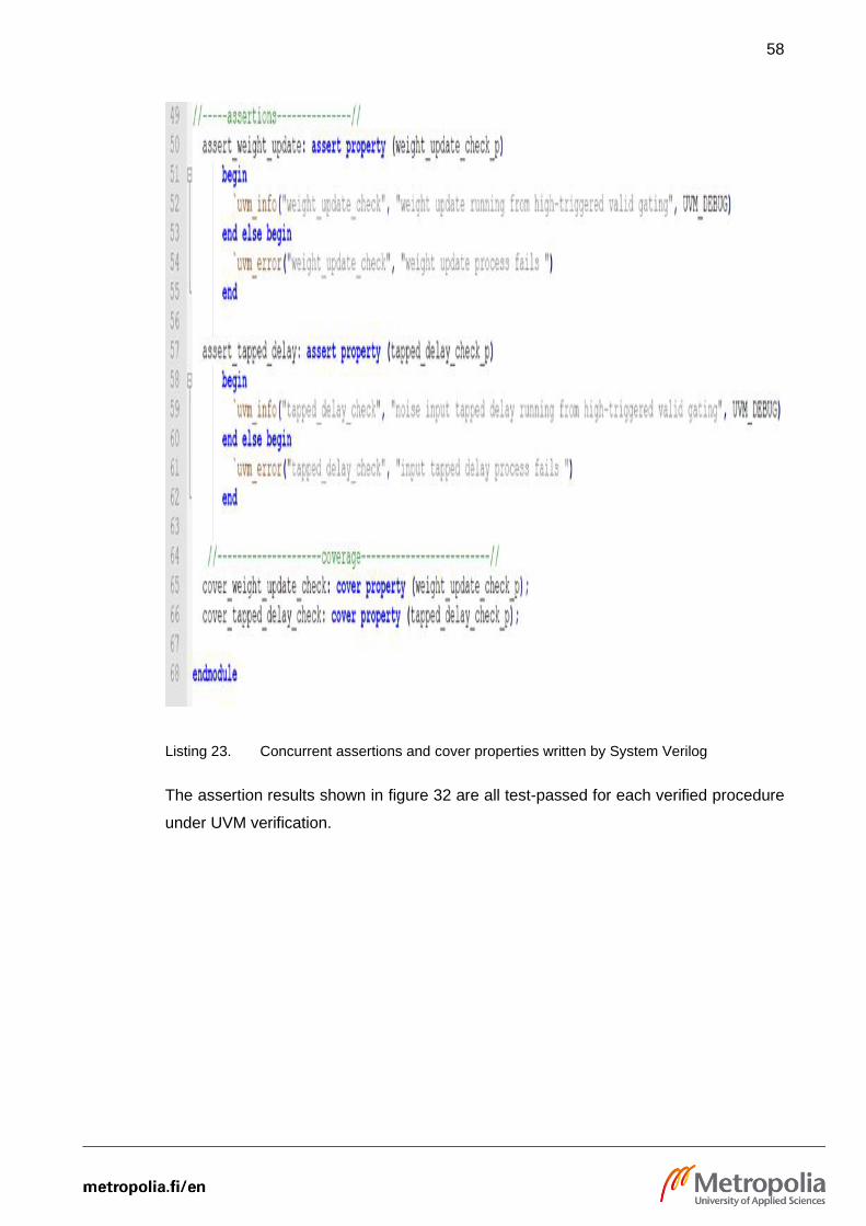
58
Listing 23. Concurrent assertions and cover properties written by System Verilog
The assertion results shown in figure 32 are all test-passed for each verified procedure
under UVM verification.
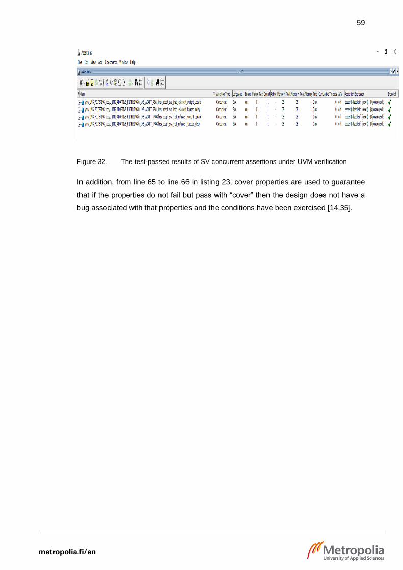
59
Figure 32. The test-passed results of SV concurrent assertions under UVM verification
In addition, from line 65 to line 66 in listing 23, cover properties are used to guarantee
that if the properties do not fail but pass with “cover” then the design does not have a
bug associated with that properties and the conditions have been exercised [14,35].

60
7 Conclusion
The Thesis work presented an adaptive FIR filtering noise cancellation module which
smoothly filtered the corrupted noisy signal to recover the clean original sinusoidal signal.
The design module implements Least Mean Squared algorithm with filter coefficients
update stages to create the compatible weights for each adaptive filtering procedure and
eliminate the uncorrelated noise from the corrupted signal. The main design goals for
this module were configurability and reusability. These were achieved already in algo-
rithm level with the use of modular coding style to create instantiated functions for partial
configurations. The configurability was implemented with the use of Matlab command
line interface which provided an interface to the configured parameters. RTL reusability
was realized by describing parameters configuration and each used function inside HDL
package. The implementation work was done adhering to Mathworks digital design flow.
Verification was likewise done following an ASIC verification flow before physical design
period. The verification flow included many modern tools and practices such as the use
of a re-usable UVM test bench for module and system level verification, specific use
case. The module was verified to produce exactly the same results as the algorithm by
comparing the fixed-point data the algorithm generated to the data the RTL model output
during functional verification. The data were compared clock accurately bit-to-bit. Addi-
tionally, no errors or bugs were found from the design module. the module passed all
required functionality tests and was cleared for RTL hand-off. The complexity of the
Adaptive FIR Filtering noise cancellation module is quite trivial to dial back and forth as
the tapped delay process, smoothing filtering stages are all modular. [11,85.]
The design module serves the purpose of noise cancellation process based on adaptive
LMS algorithm with allowed configured difference between the original input and corre-
lated filtered output. The relevant theory related adaptive filter was explored. The theory
and mathematical model of the design module were also explained. The design flow
followed the familiar top-down model where work is done in subsequent stages. First the
algorithms were developed to fixed-point models which physically realizable. Then the
RTL micro-architecture of the module was designed on the basis of the algorithms pro-
vided. The actual HDL was written following the RTL micro-architecture description. Ver-
ification work was started after all functionality was included in the RTL. The verification

61
environment was an UVM test bench which supported many modern verification tech-
niques including test case establishment, code coverage and System Verilog assertions.
[11,87.]
Hardware deployment and implementation and the related challenges, such as IP core
generation to be integrated with a register abstraction layer by using AXI protocols,
Transaction Level Modeling using SystemC and IP-XACT, could be innovated for future
development of this Thesis project, since the design module was already modified to be
modular and reusable, so that it has a scalable architecture with generic parameter spec-
ifications. This gave some valuable insight because RTL design coding style and config-
urations originally targeted to an SoC.
The aim of this work was to design, implement and verify a fully adaptive FIR filtering
noise cancellation module following Mathworks digital design flow. This objective was
successfully reached as the design module met all pre-defined design specifications.

62
References
1 Simon Haykin. Adaptive Filter Theory. Fifth Edition. Essex, England: Pearson Ed-ucation; 2014.
2 Michael Parker. Digital Signal Processing 101 Everything You Need to Know to Get Started. Second Edition. Oxford, United Kingdom: Newnes - an imprint of Elsevier; 2017.
3 Samuel D. Stearns, Don R. Hush. Digital Signal Processing with Examples in Matlab. Second Edition. Florida, USA: CRC Press; 2011.
4 Lizhe Tan, Jean Jiang. Digital Signal Processing Fundamentals and Applications. Third Edition. London, United Kingdom: Academic Press – an imprint of Elsevier; 2019.
5 Andreas Antoniou. Digital Signal Processing, Signals, Systems, and Filters. United States of America: The McGraw-Hill Companies; 2006.
6 Uwe Meyer-Baese. Digital Signal Processing with Field Programmable Gate Ar-rays. Fourth Edition. Florida, USA: Springer; 2014.
7 Vinay K. Ingle, John G. Proakis. Digital Signal Processing Using Matlab. Third Edition. Stamford, USA: Cengage Learning; 2012.
8 Roger Woods, John McAllister, Gaye Lightbody, Ying Yi. FPGA-Based Imple-mentation of Signal Processing Systems. West Sussex, United Kingdom: John Wiley & Sons; 2008.
9 Steven W. Smith. The Scientist and Engineer’s Guide to Digital Signal Pro-cessing. Second Edition. California, USA: California Technical Publishing; 1999.
10 Richard G. Lyons. Understanding Digital Signal Processing. Third Edition. Bos-ton, Massachusetts, USA: Prentice Hall; 2011.
11 Ville Kivelä. Design, Implementation and Verification of a Digital Predistorter Overdrive Protection Module. Master’s Thesis. Oulu, Finland: University of Oulu, Faculty of Information Technology and Electrical Engineering; 2016.
12 Joonas Järviluoma. Rapid Prototyping from Algorithm to FPGA Prototype. Mas-ter’s Thesis. Oulu, Finland: University of Oulu, Department of Electrical Engineer-ing; 2015
13 Joseph Petrone. Adaptive Filter Architectures for FPGA Implementation. Master’s Thesis. Florida, USA: The Florida State University College of Engineering, De-partment of Electrical and Computer Engineering; 2004.
14 Ashok B.Mehta. SystemVerilog Assertions and Functional Coverage, Guide to Language, Methodology and Applications. Third Edition. Cham, Zug, Switzerland: Springer; 2020.
15 Harry D. Foster, Adam C. Krolnik, David J. Lacey. Assertion-based Design. Sec-ond Edition. Boston, Massachusetts, USA: Kluwer Academic Publishers; 2004.

63
16 Janick Bergeron. Writing Testbenches Using System Verilog. New York, USA: Springer; 2006.
17 Mentor’s Verification Academy. Universal Verification Methodology UVM Cook-book. Mentor Graphics Corporation; 2018.
18 Mentor’s Verification Academy. Coverage Cookbook. Mentor Graphics Corpora-tion; 2019.
19 ANSI/IEEE Std 1076-1993. IEEE Standard VHDL Language Reference Manual. New York, USA: IEEE; 1994.
20 IEEE Std 1800-2005. IEEE Standard for System Verilog - Unified Hardware De-sign, Specification, and Verification Language. New York, USA: IEEE; 2005.
21 Accellera Systems Initiative. Universal Verification Methodology (UVM) 1.2 Class Reference. California, USA: Accellera; 2014.
22 Intel Corporation. Intel Quartus Prime Standard Edition User Guide: Design Rec-ommendations UG-20175. [Online]. USA: Intel; 24 September 2018. URL:https://www.intel.com/content/dam/www/programmable/us/en/pdfs/ literature/ug/ug-qps-design-recommendations.pdf [Accessed on November 9th 2020]
23 MathWorks. Verification with Cosimulation. [Online]. URL: https://www.math-works.com/help/hdlverifier/ hdl-verification-with-cosimulation.html [Accessed on November 9th 2020]
24 MathWorks. LMS Filter. [Online]. URL: https://www.math-works.com/help/dsp/ref/lmsfilter.html [Accessed on November 9th 2020]
25 Henry Chan. UVM Spells Relief - Create Robust Test Environments with Ease. [Online]. Aldec Blog. URL: https://www.aldec.com/en/company/blog/110--uvm-spells-relief [Accessed on November 9th 2020]
26 MathWorks. HDL Verifier. Test and Verify Verilog and VHDL Using HDL Simula-tors and FPGA boards. [Online]. URL: https://www.mathworks.com/products/hdl-verifier.html#resources [Accessed on November 9th 2020]
27 Roshny Jose George. Design of An Adaptive Filtering Algorithm for Noise Can-cellation. Volume 2 Issue 4. [Online]. IRJET; July 2015. URL: https://www.ir-jet.net/archives/V2/i4/Irjet-v2i4105.pdf [Accessed on November 9th 2020]