digital counter
TRANSCRIPT
8683R DIGITAL AND ANALOGUE DEVICES AND CIRCUITSEED 3303
ACKNOWLEDGEMENT
Alhamdulillah and grateful to Allah S.W.T the Al-Mighty cause give me an
opportunity of managing the specific time to complete this. Without Allah
permission definitely I cannot done my project. We can just try and pray but only
Allah can decide it.
Firstly, I must try all my best, but I know I still at back that why I need and I
must try hard with have patience inside me. I know that I must strive forward like
ask further information from lecturer and get knowledge from them. I hope in this
way I can improve myself with more encouragement and enjoyable for this
subject.
Not forgot to all my friend who help me when I got trouble and give me a
spirit to get more interesting in this subject, meanwhile to my senior who are give
me an advice for this subject that really important for getting a job next.
I hope that when I done this project the knowledge of this project not just
disappears and I always can refer it back and give me the knowledge to
extending my educational higher level and also useful as an experience for the
future coming.
I accept equal responsibility for this texts strength and weaknesses .The
entire good thing came from Allah and the weakness is from my own weakness,
because it is natural human been.
Lastly, I hope that my lecturer always supports me to go forward, and I get
more interesting to learn more for have the credibility and creativity in this
subject.
1

8683R DIGITAL AND ANALOGUE DEVICES AND CIRCUITSEED 3303
INTRODUCTION
A synchronous binary counter has the same sequence of count states as
a ripple counter. However, if a flip-flop changes state when a synchronous
counter is incremented, the chance occurs on the leading or trailing edge of a
clock pulse rather than on the leading or trailing edge of the preceding flip-flop’s
output
As is characteristic of all synchronous devices, the clock is connected to
every flip-flop in the counter, and all those flip-flop that change state do so at the
same time. In a synchronous counter, the flip-flop are most often of the J-K type.
The circuit is a synchronous counter that will count up 00 to 99, then down
99 to 00, then up 00 to 99. There are 3 type of Integrated Circuit use in this circuit
(SN 7447, 74LS192, and 74LS04). It also can be manually stop and reset by an
externally push button. The circuit can be divided into two sections. One section
is called the unit counter; the other is the decade counter.
There are 4 types of Integrated Circuit (IC) used in this circuit, 74LS192,
SN 7447, 74LS04 and 555.
74LS192 IC is a synchronous BCD up/down counter. It is used to count
up/down the binary output.
SN7447 IC is a BCD to seven-segment decoder. It is used to connect the
output from 74LS192 to a seven-segment display. The type of seven-segment
display that has been used is common cathode seven-segment display
2

8683R DIGITAL AND ANALOGUE DEVICES AND CIRCUITSEED 3303
555 is a timer IC. The clock from the IC will replace the clock from the
digital trainer.
Seven-segment display is used to view the output of the circuit. Instead of
the output is display in binary state, the seven –segment display can display it in
decimal state without any requirement of translating binary to decimal or any
other format.
3

8683R DIGITAL AND ANALOGUE DEVICES AND CIRCUITSEED 3303
UP/DOWN SYNCHRONOUS COUNTER CIRCUIT
4

8683R DIGITAL AND ANALOGUE DEVICES AND CIRCUITSEED 3303
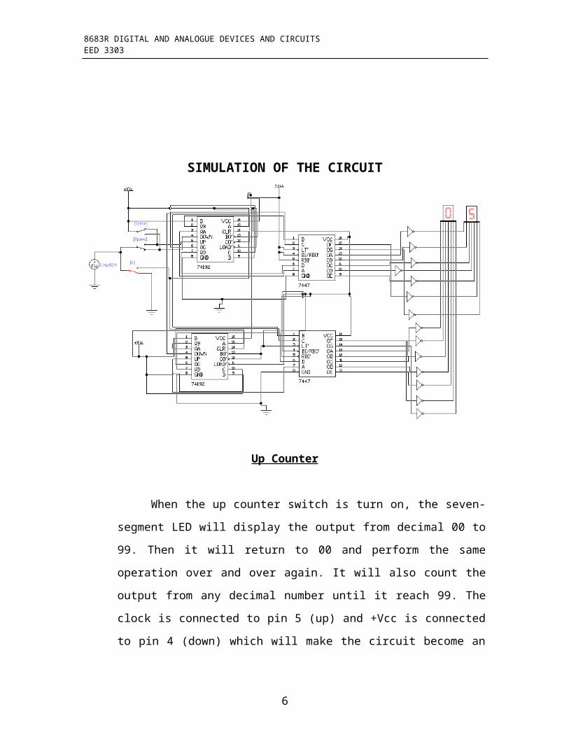
SIMULATION OF THE CIRCUIT
Up Counter
When the up counter switch is turn on, the seven-segment LED will
display the output from decimal 00 to 99. Then it will return to 00 and
perform the same operation over and over again. It will also count the
output from any decimal number until it reach 99. The clock is connected
to pin 5 (up) and +Vcc is connected to pin 4 (down) which will make the
circuit become an up counter. IC 74LS192 will received a clock from the
timer IC. This IC will count up from 0 for a unit counter. When the unit
counter reached to 9, pin 12 and 3 will generate the clock to the second IC
74LS192 at below. This second IC will start count up from 0 for a decade
counter. Then the circuit wills continuous count up from 00 till it reached to
the highest value 99.
5
8683R DIGITAL AND ANALOGUE DEVICES AND CIRCUITSEED 3303
Down Counter
When the down counter switch is turn on, the seven-segment LED will
display the output from decimal 99 to 00. Then it will return to 99 and perform the
same operation over and over again. It will also count the output from any
decimal number until it reaches 00. The clock is connected to pin 4 (down) and
+Vcc is connected to pin 5 (up) which will make the circuit become a down
counter. IC 74LS192 will received a clock from the timer IC. This IC will count
down from 9 for a unit counter. When the unit counter reached to 0, the pin 12
and pin 13 will generate the clock to the second IC 74LS192 at below. This
second IC will start count down from 9 for a decade counter. Then the circuit wills
continue count down from 99 till it reached to the lowest value 00.
6

8683R DIGITAL AND ANALOGUE DEVICES AND CIRCUITSEED 3303
Reset condition
When the clear switch is turn on, the seven segments LED will reset back
to 00. This condition applies to both up and down counter. This is cause by the
Vcc which is connected to clear (pin 14) on the 74LS192 IC make the IC to reset
to its original condition. But, when the reset button was pushed, the voltage
supply will flow through the pin 14 for both of IC 74LS192. When the voltage
enters to both of this IC, it will automatically reset the counter circuit. So, when
the counter circuit is reset the seven segment will display 00 as at above.
7

8683R DIGITAL AND ANALOGUE DEVICES AND CIRCUITSEED 3303
ANALYSIS
Synchronous Counter
A Synchronous binary counter has the same sequence of count states as a ripple
counter. However, if a flip-flops changes state when a synchronous counter is
incremented, the change occurs on the leading or trailing edge of a clock pulse
rather than on the leading or trailing edge of the preceding flip-flops output.
The characteristic a synchronous, the clock is connected to every flip-flop
in the counter. In a synchronous counter, the flip-flops are most often of under
normal operating conditions, the J and K inputs to each flip-flop should remain
stable at either logic 1 or 0 while the count pulse undergoes its 1 to 0 to 1
transition.
Logic 1 on the clear control line will force all counter outputs to logic 0 and
hold them there until the clear line is returned to logic pulses and leave the
counter in some nonzero state, if such data-hold behavior is required for
particular application the J-K type.
8

8683R DIGITAL AND ANALOGUE DEVICES AND CIRCUITSEED 3303
COMPONENT IN THE CIRCUIT
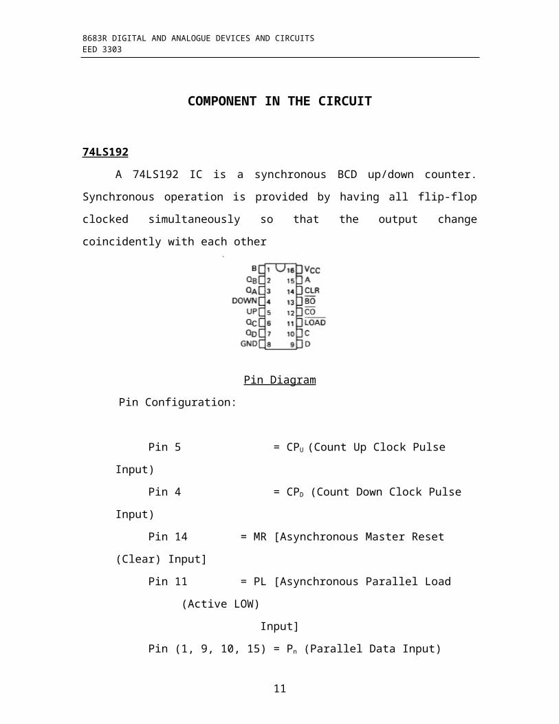
74LS192
A 74LS192 IC is a synchronous BCD up/down counter. Synchronous
operation is provided by having all flip-flop clocked simultaneously so that the
output change coincidently with each other
Pin Diagram
Pin Configuration:
Pin 5 = CPU (Count Up Clock Pulse Input)
Pin 4 = CPD (Count Down Clock Pulse Input)
Pin 14 = MR [Asynchronous Master Reset (Clear) Input]
Pin 11 = PL [Asynchronous Parallel Load (Active LOW)
Input]
Pin (1, 9, 10, 15) = Pn (Parallel Data Input)
Pin (2, 3, 6, 7) = Qn (Flip-Flop Outputs)
Pin 13 = TCD [Terminal Count Down (Borrow) Output]
Pin 12 = TCU [Terminal Count Up (Carry) Output]
Pin 8 = Gnd (Terminal Ground)
Pin 16 = Vcc (Input Voltage Terminal)
9

8683R DIGITAL AND ANALOGUE DEVICES AND CIRCUITSEED 3303
SN7447
A SN7447 IC is BCD to seven-segment decoder.
Pin Diagram
Pin Configuration:
Pin 3 = LT (Lamp Test)
Pin 5 = RBI (Ripple Blanking Input)
Pin 4 = BI/RBO (Blanking Input/Ripple Blanking
Output)
Pin (1, 2, 6, 7) = Input Terminal
Pin (9, 10, 11, 12, 13, 14,15) = Output Terminal
Pin 8 = Gnd (Ground Terminal)
Pin 16 = Vcc (Input Voltage Terminal)
10
8683R DIGITAL AND ANALOGUE DEVICES AND CIRCUITSEED 3303
555 Timer IC
555 is a timer IC. It will replace the clock from the digital trainer.
Pin Diagram
Pin Configuration:
Pin 1 = Gnd (Ground Terminal)
Pin 8 = Vcc (Input Voltage Terminal)
Pin 3 = Output (Clock/Timer Output)
11

8683R DIGITAL AND ANALOGUE DEVICES AND CIRCUITSEED 3303
74LS04
74LS04 is an inverter IC. It has 6 inverter gates inside an IC. It will invert
the input to the opposite condition as it output. (0 to 1, 1 to 0).
Pin Diagram
Pin Configuration:
Pin 1 = First Input (A0)
Pin 2 = First Output (Ā0)
Pin 3 = Second Input (A1)
Pin 4 = Second Output (Ā1)
Pin 5 = Third Input (A2)
Pin 6 = Third Output (Ā2)
Pin 7 = Gnd (Ground Terminal)
Pin 8 = Forth Input (A3)
Pin 9 = Forth Output (Ā3)
Pin 10 = Fifth Input (A4)
Pin 11 = Fifth Output (Ā4)
Pin 12 = Sixth Input (A5)
Pin 13 = Sixth Output (Ā5)
Pin 14 = Vcc (Input Voltage Terminal)
12

8683R DIGITAL AND ANALOGUE DEVICES AND CIRCUITSEED 3303
Seven-Segment Display
The seven-segment display chosen for this project is common Anode.
Seven Segment Common Anode LED Display Physical Layout and Schematic Diagram
The type of seven-segment display that has been used in this project is a common cathode seven-segment display. This seven segment will turn on when connected with the BCD-Decimal decoder and input voltage. This seven-segment has 10 pins. Pin number 3 is connected to the input voltage. Pins are connected to SN7447 IC according to their description.
13
When the number zero is display, all of pin is turn on except for pin g. This means the input High are connected through all of pin (a, b, c, d, e, and f). While the input Low is connected through the pin g.

8683R DIGITAL AND ANALOGUE DEVICES AND CIRCUITSEED 3303
14
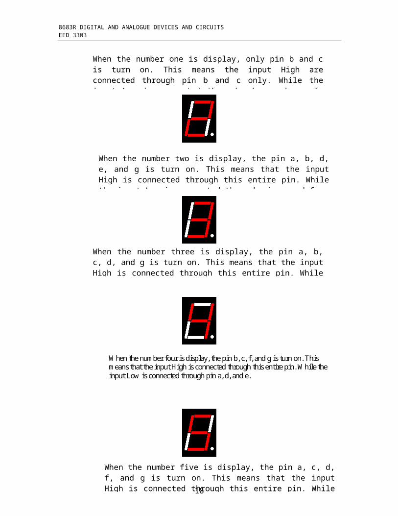
When the number one is display, only pin b and c is turn on. This means the input High are connected through pin b and c only. While the input Low is connected through pin a, d, e, f, and g.
When the number two is display, the pin a, b, d, e, and g is turn on. This means that the input High is connected through this entire pin. While the input Low is connected through pin c and f.
When the number three is display, the pin a, b, c, d, and g is turn on. This means that the input High is connected through this entire pin. While the input Low is connected through pin e and f.
When the number four is display, the pin b, c, f, and g is turn on. This means that the input High is connected through this entire pin. While the input Low is connected through pin a, d, and e.

8683R DIGITAL AND ANALOGUE DEVICES AND CIRCUITSEED 3303
15
When the number five is display, the pin a, c, d, f, and g is turn on. This means that the input High is connected through this entire pin. While the input Low is connected through pin b and e.
When the number is six displays, the pin c, d, e, f, and g are turn on. This means that the input High is connected through this entire pins. While the input Low is connected through pin a and b.
When the number seven is display, the pin a, b, and c is turn on. This means that the input High is connected through this entire pins. While the input Low is connected through pin d, e, f, and g.
When the number is eight displays, the entire pin a, b, c, d, e, f, and g is turn on. This means that the input High is connected through this entire pin.

8683R DIGITAL AND ANALOGUE DEVICES AND CIRCUITSEED 3303
16
When the number nine is display, the pin a, b, c, d, f, and g is turn on. This means that the input High is connected through this entire pin. While the input Low is connected through the pin e.

8683R DIGITAL AND ANALOGUE DEVICES AND CIRCUITSEED 3303
COMPONENTS LIST
This is the list of components that I used to complete my synchronous up/down counter.
Component Quantity Price (RM)
74LS192 IC 2Given by
Lecturer
SN 7447 IC 2Given by
Lecturer
Resistor (1k Ω & 10k Ω) 2Given by
Lecturer
Metric Street Board (MSB) 1Given by
Lecturer
Common cathode seven
segment display2
Given by
Lecturer
Reset switch 1 0.30
Up/down switch 1 1.80
555 timer IC 1Given by
Lecturer
Capacitor (22µF) 1Given by
Lecturer
IC base (14 pins) 3 0.90
IC base (16 pins) 4 2.40
17
8683R DIGITAL AND ANALOGUE DEVICES AND CIRCUITSEED 3303
CONCLUSION
After I finish this assignment, I get more knowledge and more information
during do this assignment. What I get is I know how to design ripple counter.
Before we design we must know the step that we must follow. The first step is we
must do the state diagram. In here we know what mode that we want to design.
With using this state diagram my work very easy and we can see what we need
to do.
The second step that we need to do is transition table. After we do this we
must do the present and next present to get the output before using the
Karnough Map. After we get the output then we put it in the Karnough map then
we simplified it. After we have followed all the procedure we can design the MOD
that we need. The type of IC that we need to use is 74LS47 and 74LS192.
I also find the best way to troubleshoot my circuit counter with the lab
assignment. This is because while I build my circuit at stripe board. I learn how to
settle my problem. Such as connection between ic pin and other component.
This lab assignment give me many experience and I can used this knowledge for
build any circuit with greatest
For my observation, when we design we can use any logic that we want.
But if we want do the project we must use the simple logic because to save the
budget. We also must be careful during do design because if we have a careless
mistake we can get what the MOD that we want. Therefore that output also can
get.
18