digital background calibration techniques for...
TRANSCRIPT
DIGITAL BACKGROUND CALIBRATION TECHNIQUES FOR
HIGH-RESOLUTION, WIDE BANDWIDTH
ANALOG-TO-DIGITAL CONVERTERS
By
Alma Delic-Ibukic
B.S. University of Maine, 2002
M.S. University of Maine, 2004
A THESIS
Submitted in Partial Fulfillment of the
Requirements for the Degree of
Doctor of Philosophy
(in Electrical Engineering)
The Graduate School
The University of Maine
August, 2008
Advisory Committee:
Donald M. Hummels, Castle Professor of Electrical and Computer Engineering,
Advisor
David E. Kotecki, Associate Professor of Electrical and Computer Engineering
Duane Hanselman, Associate Professor of Electrical and Computer Engineering
Ali Abedi, Assistant Professor of Electrical and Computer Engineering
Ali Ozluk, Professor of Mathematics and Statistics

LIBRARY RIGHTS STATEMENT
In presenting this thesis in partial fulfillment of the requirements for an advanced
degree at The University of Maine, I agree that the Library shall make it freely available
for inspection. I further agree that permission for “fair use” copying of this thesis for
scholarly purposes may be granted by the Librarian. It is understood that any copying
or publication of this thesis for financial gain shall not be allowed without my written
permission.
Signature:
Date:

DIGITAL BACKGROUND CALIBRATION TECHNIQUES FOR
HIGH-RESOLUTION, WIDE BANDWIDTH
ANALOG-TO-DIGITAL CONVERTERS
By Alma Delic-Ibukic
Thesis Advisor: Dr. Donald M. Hummels
An Abstract of the Thesis Presentedin Partial Fulfillment of the Requirements for the
Degree of Doctor of Philosophy(in Electrical Engineering)
August, 2008
Due to consumer demand for wireless devices that support multimedia services rang-
ing from voice and data transfer to video on demand, there is a need for flexible and
adaptable base stations. These systems are typically implemented using a wide-band re-
ceiver that captures and digitizes the entire cellular band which contains multiple wire-
less standards. In order to digitize the entire cellular band, there is a requirement for
wide bandwidth, high-resolution analog-to-digital converters (ADCs). In general, these
ADCs are hard to realize and require some form of calibration to meet the requirements.
In this thesis, two novel digital background calibration techniques targeted for pipeline
and Π∆Σ architecture ADCs are reported. The two calibration schemes are realized
by introducing a redundancy in the system. For the pipeline architecture converters,
two extra stages located at the end of the pipeline are implemented and are active only
during calibration process. This calibration is suitable for implementation in a fully
monolithic pipeline ADCs. For the Π∆Σ architecture converters, an extra channel that
is linearly dependent on the Π∆Σ channels is implemented to correct for channel gain
mismatches. All channels are calibrated simultaneously, and calibration of the overall
system depends on the convergence rate of a recursive-least-squares algorithm.

ACKNOWLEDGMENTS
I would first like to thank my advisor Professor Donald M. Hummels for being a
great mentor and for introducing me to data converters. His support and technical guid-
ance throughout this project have been invaluable. He always managed to find some-
thing positive in every situation. His trust in me helped me move forward in my research
and most importantly helped me build confidence. It has been a privilege working with
him.
I would also like to thank Professor David E. Kotecki for patiently answering all
my Cadence questions and any other questions I always seemed to have. Your guidance
and advice have been greatly appreciated.
Thank you, Professor Ali Abedi for serving on my committee and especially for
making the resources of your lab available for the successful completion of my research.
Thank you, Professor Duane Hanselman and Professor Ali Ozluk for serving on
my committee and for sharing with me your knowledge of engineering and mathematics
throughout my education at the University of Maine.
I would like to thank Steven Turner for finding time to review my thesis and
provide valuable feedback. Also, I would like to thank Heidi Purrington for helping out
and doing an excellent job with the layout of an ADC test board.
Also, I would like to express my gratitude to my colleagues and friends, Thomas
Kenny, Thomas Pollard, Homer W. Slade, Bennett Meulendyk and Janice Duy for all
those productive days in Barrows Hall. I will truly miss you.
I would like to thank to my international friends, Metin Cakir, Sonia Aziz, San-
jeev Manandhar, Silvia Cordero-Sancho and Semra Ozdemir for being part of my life,
and sharing with me all my hardships and every one of my accomplishments.
Finally, and most importantly, I would like to express my gratitude to my family,
Nihada and Sead Delic-Ibukic, Judy Cox and my brother Dino for their love, support
University of Maine Ph.D. DissertationAlma Delic-Ibukic, August, 2008
ii

and encouragement throughout this educational endeavor. They have been my number
one fans throughout this educational roller coster ride, and this thesis is dedicated to
them.
University of Maine Ph.D. DissertationAlma Delic-Ibukic, August, 2008
iii
TABLE OF CONTENTS
ACKNOWLEDGMENTS . . . . . . . . . . . . . . . . . . . . . . . . . . . . . . . . . . . . . . . . . . . . . . . . . . . . . . . . . . . . . . ii
LIST OF TABLES. . . . . . . . . . . . . . . . . . . . . . . . . . . . . . . . . . . . . . . . . . . . . . . . . . . . . . . . . . . . . . . . . . . . . . . vi
LIST OF FIGURES . . . . . . . . . . . . . . . . . . . . . . . . . . . . . . . . . . . . . . . . . . . . . . . . . . . . . . . . . . . . . . . . . . . . . vii
Chapter
1 Introduction . . . . . . . . . . . . . . . . . . . . . . . . . . . . . . . . . . . . . . . . . . . . . . . . . . . . . . . . . . . . . . . . . . . . . . . . . . 11.1 Background . . . . . . . . . . . . . . . . . . . . . . . . . . . . . . . . . . . . . . . . . . . . . . . . . . . . . . . . . . . . . . . . . . . 31.2 Purpose of the Research . . . . . . . . . . . . . . . . . . . . . . . . . . . . . . . . . . . . . . . . . . . . . . . . . . . . . . 61.3 Thesis Organization . . . . . . . . . . . . . . . . . . . . . . . . . . . . . . . . . . . . . . . . . . . . . . . . . . . . . . . . . . . 8
2 Wide-Bandwidth, High-Resolution Analog-to-Digital Converter Architectures . 102.1 Analog-to-Digital Conversion Process . . . . . . . . . . . . . . . . . . . . . . . . . . . . . . . . . . . . . . . 102.2 Successive-Approximation-Register (SAR) ADCs . . . . . . . . . . . . . . . . . . . . . . . . . 132.3 Pipeline Architecture ADCs . . . . . . . . . . . . . . . . . . . . . . . . . . . . . . . . . . . . . . . . . . . . . . . . . . 142.4 Oversampled Converter Architectures . . . . . . . . . . . . . . . . . . . . . . . . . . . . . . . . . . . . . . . 16
2.4.1 Quantization . . . . . . . . . . . . . . . . . . . . . . . . . . . . . . . . . . . . . . . . . . . . . . . . . . . . . . . . . . 172.4.2 Oversampled A/D Converter Architecture . . . . . . . . . . . . . . . . . . . . . . . . . . 182.4.3 ∆Σ Architecture ADCs . . . . . . . . . . . . . . . . . . . . . . . . . . . . . . . . . . . . . . . . . . . . . . 19
2.5 Parallel ∆Σ ADC Architectures. . . . . . . . . . . . . . . . . . . . . . . . . . . . . . . . . . . . . . . . . . . . . . 242.5.1 Time-Interleaved ADC Architectures . . . . . . . . . . . . . . . . . . . . . . . . . . . . . . . 242.5.2 Frequency-Band-Decomposition ADC Architecture . . . . . . . . . . . . . . . 262.5.3 Hadamard Modulated ∆Σ ADC Architecture . . . . . . . . . . . . . . . . . . . . . . 28
3 Pipeline A/D Converter Calibration Techniques . . . . . . . . . . . . . . . . . . . . . . . . . . . . . . . . . . . 303.1 Pipeline Architecture Overview (1-bit per stage example) . . . . . . . . . . . . . . . . . 303.2 Sources of Error in Pipeline A/D Converters . . . . . . . . . . . . . . . . . . . . . . . . . . . . . . . . 33
3.2.1 Sub-ADC Error. . . . . . . . . . . . . . . . . . . . . . . . . . . . . . . . . . . . . . . . . . . . . . . . . . . . . . . 333.2.2 Sub-DAC error . . . . . . . . . . . . . . . . . . . . . . . . . . . . . . . . . . . . . . . . . . . . . . . . . . . . . . . 363.2.3 Interstage Gain Error. . . . . . . . . . . . . . . . . . . . . . . . . . . . . . . . . . . . . . . . . . . . . . . . . 37
3.3 Analog Calibration Schemes . . . . . . . . . . . . . . . . . . . . . . . . . . . . . . . . . . . . . . . . . . . . . . . . . 383.4 Digital Calibration Schemes. . . . . . . . . . . . . . . . . . . . . . . . . . . . . . . . . . . . . . . . . . . . . . . . . . 40
3.4.1 Off-line Calibration . . . . . . . . . . . . . . . . . . . . . . . . . . . . . . . . . . . . . . . . . . . . . . . . . . 433.4.2 Real-Time Digital Calibration Scheme Development . . . . . . . . . . . . . . 45
3.5 Verilog Implementation and Results . . . . . . . . . . . . . . . . . . . . . . . . . . . . . . . . . . . . . . . . . 503.5.1 Finite State Machine (FSM) Description . . . . . . . . . . . . . . . . . . . . . . . . . . . 503.5.2 Required Stage Modifications . . . . . . . . . . . . . . . . . . . . . . . . . . . . . . . . . . . . . . . 523.5.3 Error Correction Logic Modification. . . . . . . . . . . . . . . . . . . . . . . . . . . . . . . . 533.5.4 Results of the Developed Calibration Technique . . . . . . . . . . . . . . . . . . . 55
University of Maine Ph.D. DissertationAlma Delic-Ibukic, August, 2008
iv
3.5.5 Complexity of the Real-Time Calibration Logic . . . . . . . . . . . . . . . . . . . 57
4 Hadamard Modulated ∆Σ A/D Converter Calibration Techniques . . . . . . . . . . . . . . . 584.1 Overview of Modulation Based A/D Converter Architectures . . . . . . . . . . . . . 584.2 Oversampling Π∆Σ A/D Converter Architecture . . . . . . . . . . . . . . . . . . . . . . . . . . . 61
4.2.1 Overview of Π∆Σ A/D Converters . . . . . . . . . . . . . . . . . . . . . . . . . . . . . . . . . 624.2.2 Simulation of Π∆Σ A/D Converters . . . . . . . . . . . . . . . . . . . . . . . . . . . . . . . . 66
4.3 Dominant Errors in Π∆Σ ADCs . . . . . . . . . . . . . . . . . . . . . . . . . . . . . . . . . . . . . . . . . . . . . 714.3.1 Channel Gain and Offset Mismatch Errors . . . . . . . . . . . . . . . . . . . . . . . . . 714.3.2 Calibration Techniques for Modulation-Based ADCs. . . . . . . . . . . . . . 76
4.4 Real-Time Digital Calibration Algorithm Development . . . . . . . . . . . . . . . . . . . . 784.5 Effect of Quantization Noise on Π∆Σ ADCs . . . . . . . . . . . . . . . . . . . . . . . . . . . . . . . 814.6 Overview of the RLS Algorithm . . . . . . . . . . . . . . . . . . . . . . . . . . . . . . . . . . . . . . . . . . . . . 854.7 The RLS Algorithm Applied to Π∆Σ ADCs. . . . . . . . . . . . . . . . . . . . . . . . . . . . . . . . 894.8 Simulation Results for the RLS Algorithm Performance . . . . . . . . . . . . . . . . . . . 974.9 Calibration Algorithm and Dynamic Range Improvement . . . . . . . . . . . . . . . . . 1054.10 Calibration Based on Multi-Tone Input Signal . . . . . . . . . . . . . . . . . . . . . . . . . . . . . . 112
5 Hardware Implementation and Results . . . . . . . . . . . . . . . . . . . . . . . . . . . . . . . . . . . . . . . . . . . . . 1185.1 Π∆Σ ADC Architecture . . . . . . . . . . . . . . . . . . . . . . . . . . . . . . . . . . . . . . . . . . . . . . . . . . . . . . 1185.2 Design Overview. . . . . . . . . . . . . . . . . . . . . . . . . . . . . . . . . . . . . . . . . . . . . . . . . . . . . . . . . . . . . . 123
5.2.1 OTA DC Gain Requirements . . . . . . . . . . . . . . . . . . . . . . . . . . . . . . . . . . . . . . . . 1245.2.2 kT/C Noise and Capacitor Sizing . . . . . . . . . . . . . . . . . . . . . . . . . . . . . . . . . . . 1265.2.3 OTA Slew Rate Requirements . . . . . . . . . . . . . . . . . . . . . . . . . . . . . . . . . . . . . . . 1275.2.4 Fully Differential Gain Boosting OTA . . . . . . . . . . . . . . . . . . . . . . . . . . . . . . 1295.2.5 Remaining ∆Σ Modulator Components . . . . . . . . . . . . . . . . . . . . . . . . . . . . 136
5.3 Test and Characterization . . . . . . . . . . . . . . . . . . . . . . . . . . . . . . . . . . . . . . . . . . . . . . . . . . . . . 1375.4 Performance Test. . . . . . . . . . . . . . . . . . . . . . . . . . . . . . . . . . . . . . . . . . . . . . . . . . . . . . . . . . . . . . 139
5.4.1 Real-Time Calibration Results for an 8-channel Π∆Σ ADC . . . . . . 1405.4.2 Real-Time Calibration Results for a 16-channel Π∆Σ ADC . . . . . . 141
6 Conclusion . . . . . . . . . . . . . . . . . . . . . . . . . . . . . . . . . . . . . . . . . . . . . . . . . . . . . . . . . . . . . . . . . . . . . . . . . . . 1546.1 Summary of Accomplishments. . . . . . . . . . . . . . . . . . . . . . . . . . . . . . . . . . . . . . . . . . . . . . . 1556.2 Recommendations for Future Work . . . . . . . . . . . . . . . . . . . . . . . . . . . . . . . . . . . . . . . . . . 159
REFERENCES . . . . . . . . . . . . . . . . . . . . . . . . . . . . . . . . . . . . . . . . . . . . . . . . . . . . . . . . . . . . . . . . . . . . . . . . . . 161
APPENDIX A. Circuit Schematics . . . . . . . . . . . . . . . . . . . . . . . . . . . . . . . . . . . . . . . . . . . . . . . . 169
APPENDIX B. Test Board Schematics and Layout. . . . . . . . . . . . . . . . . . . . . . . . . . . . . . . 179
Biography of the Author . . . . . . . . . . . . . . . . . . . . . . . . . . . . . . . . . . . . . . . . . . . . . . . . . . . . . . . . . . . . . . . . 186
University of Maine Ph.D. DissertationAlma Delic-Ibukic, August, 2008
v

LIST OF TABLES
3.1 Sample propagation through the pipeline for the proposed real-time digital calibration technique. . . . . . . . . . . . . . . . . . . . . . . . . . . . . . . . . . . . . . . . . . 48
4.1 Summary of the RLS algorithm . . . . . . . . . . . . . . . . . . . . . . . . . . . . . . . . . . . . . . . . . . . . 86
4.2 Summary of the RLS algorithm convergence for n � M + 1with and without quantization noise present. . . . . . . . . . . . . . . . . . . . . . . . . . . . . . . 96
5.1 Characteristics of a fully differential gain-boosting OTA withCMFB. . . . . . . . . . . . . . . . . . . . . . . . . . . . . . . . . . . . . . . . . . . . . . . . . . . . . . . . . . . . . . . . . . . . . . . . 135
5.2 Equipment used to test custom designed chip that contains tensecond-order ∆Σ modualtors. . . . . . . . . . . . . . . . . . . . . . . . . . . . . . . . . . . . . . . . . . . . . . . 139
6.1 Summary of the RLS algorithm convergence for n � M + 1with and without quantization noise present. . . . . . . . . . . . . . . . . . . . . . . . . . . . . . . 158
A.1 Device sizing for obtaining V b1 and V b2 biasing voltages inFigure A.1. These will bias the fully differential tranconduc-tance amplifier and CMFB circuit in Figures 5.8 and 5.10. . . . . . . . . . . . . . . 170
A.2 Device sizing for obtaining V b3 and V b4 biasing voltages inFigure A.1. These will bias the differential gain boosting am-plifiers in Figure 5.9. . . . . . . . . . . . . . . . . . . . . . . . . . . . . . . . . . . . . . . . . . . . . . . . . . . . . . . . 170
University of Maine Ph.D. DissertationAlma Delic-Ibukic, August, 2008
vi
LIST OF FIGURES
1.1 Traditional multicarrier base station receiver architecture. . . . . . . . . . . . . 2
1.2 Software radio receiver architecture for a base station sys-tem using wide-bandwidth IF sampling ADCs. . . . . . . . . . . . . . . . . . . . . . . . . 2
1.3 Blocking profile for GSM 900 Base Transceiver Stations(BTS) [1]. . . . . . . . . . . . . . . . . . . . . . . . . . . . . . . . . . . . . . . . . . . . . . . . . . . . . . . . . . . . . . . . . 4
2.1 Basic concept behind A/D conversion. . . . . . . . . . . . . . . . . . . . . . . . . . . . . . . . . . 11
2.2 Commercially available ADCs from Analog Devices, Inc.and Texas Instruments Incorporated reported in September2007. . . . . . . . . . . . . . . . . . . . . . . . . . . . . . . . . . . . . . . . . . . . . . . . . . . . . . . . . . . . . . . . . . . . . . . 12
2.3 Successive-approximation-register A/D converter block di-agram. . . . . . . . . . . . . . . . . . . . . . . . . . . . . . . . . . . . . . . . . . . . . . . . . . . . . . . . . . . . . . . . . . . . . 14
2.4 Generic pipeline ADC block diagram. . . . . . . . . . . . . . . . . . . . . . . . . . . . . . . . . . . 15
2.5 Generic pipeline stage block diagram. . . . . . . . . . . . . . . . . . . . . . . . . . . . . . . . . . . 16
2.6 An example of a uniform 2-bit quantizer and quantizationerror e showing the deviation of the actual 2-bit quantizerfrom the straight line (ideal quantizer). . . . . . . . . . . . . . . . . . . . . . . . . . . . . . . . . . . 17
2.7 Oversampled A/D converter architecture. . . . . . . . . . . . . . . . . . . . . . . . . . . . . . . 19
2.8 Quantization noise power spectral density for A/D convert-ers with and without oversampling employed. . . . . . . . . . . . . . . . . . . . . . . . . . 20
2.9 ∆Σ converter architecture implemented using first order∆Σ modulators. . . . . . . . . . . . . . . . . . . . . . . . . . . . . . . . . . . . . . . . . . . . . . . . . . . . . . . . . . . 20
2.10 Linear model for a first order ∆Σ modulator. . . . . . . . . . . . . . . . . . . . . . . . . . . 21
2.11 Frequency response of NTF (z) and STF (z) for the firstorder ∆Σ modulator. The normalized frequency is givenby f = F
DFS, where FS is the Nyquist-rate frequency for
the first order ∆Σ modulator and D is the oversamplingratio. . . . . . . . . . . . . . . . . . . . . . . . . . . . . . . . . . . . . . . . . . . . . . . . . . . . . . . . . . . . . . . . . . . . . . . 22
2.12 Frequency response of a comb2 filter with D = 20. . . . . . . . . . . . . . . . . . . . 24
2.13 An M -channel time-interleaved ADC system. . . . . . . . . . . . . . . . . . . . . . . . . . 25
2.14 ModifiedM -channel time-interleaved ADC system that avoidsclock skew errors. . . . . . . . . . . . . . . . . . . . . . . . . . . . . . . . . . . . . . . . . . . . . . . . . . . . . . . . . 26
University of Maine Ph.D. DissertationAlma Delic-Ibukic, August, 2008
vii

2.15 M -channel frequency-band-decomposition ADC architec-ture. . . . . . . . . . . . . . . . . . . . . . . . . . . . . . . . . . . . . . . . . . . . . . . . . . . . . . . . . . . . . . . . . . . . . . . . 27
2.16 Frequency response of the bank of M analysis filters witheach assigned to different frequency band. . . . . . . . . . . . . . . . . . . . . . . . . . . . . . 27
2.17 Π∆Σ A/D converter architecture. . . . . . . . . . . . . . . . . . . . . . . . . . . . . . . . . . . . . . . . 28
3.1 Generic Pipeline ADC block diagram showing the detailsof a pipeline stage. . . . . . . . . . . . . . . . . . . . . . . . . . . . . . . . . . . . . . . . . . . . . . . . . . . . . . . . 31
3.2 Residual error plots for 1-bit per stage ideal pipeline ADC(blue) and pipeline ADC with errors (red). . . . . . . . . . . . . . . . . . . . . . . . . . . . . . . 34
3.3 Residual error characteristics and allowed threshold voltagevariations. . . . . . . . . . . . . . . . . . . . . . . . . . . . . . . . . . . . . . . . . . . . . . . . . . . . . . . . . . . . . . . . . 36
3.4 Switched capacitor implementation of the MDAC for 1-bitper stage architecture. . . . . . . . . . . . . . . . . . . . . . . . . . . . . . . . . . . . . . . . . . . . . . . . . . . . . 37
3.5 Pipeline ADC with off-line digital calibration applied to theseventh stage. . . . . . . . . . . . . . . . . . . . . . . . . . . . . . . . . . . . . . . . . . . . . . . . . . . . . . . . . . . . . . 42
3.6 Example of a two-phase, non-overlapping clock signal usedin pipeline ADC architecture. . . . . . . . . . . . . . . . . . . . . . . . . . . . . . . . . . . . . . . . . . . . 45
3.7 Proposed real-time digital calibration architecture. . . . . . . . . . . . . . . . . . . . . . 49
3.8 Modifications required for a stage to be calibrated (dashedboxes). . . . . . . . . . . . . . . . . . . . . . . . . . . . . . . . . . . . . . . . . . . . . . . . . . . . . . . . . . . . . . . . . . . . . 52
3.9 Modified error correction logic for a real-time digital cali-bration scheme implementation. Example of N -stage con-verter with 1-bit per stage architecture. . . . . . . . . . . . . . . . . . . . . . . . . . . . . . . . . . . 54
3.10 Residual error characteristics for a simulated ADC with ap-plied real-time calibration and errors introduced in all 18stages of the converter. . . . . . . . . . . . . . . . . . . . . . . . . . . . . . . . . . . . . . . . . . . . . . . . . . . . 56
4.1 Generic architecture for modulation based ∆Σ converters. . . . . . . . . . . . . 59
4.2 Π∆Σ A/D converter architecture with oversampling. . . . . . . . . . . . . . . . . . . 62
4.3 Linear model for a second order ∆Σ modulator used in sim-ulations. . . . . . . . . . . . . . . . . . . . . . . . . . . . . . . . . . . . . . . . . . . . . . . . . . . . . . . . . . . . . . . . . . . . 67
4.4 Frequency spectrum of 8 by 8 Hadamard matrix. Numbers1 through 8 indicate Hadamard matrix rows and FS is theNyquist-rate clock. . . . . . . . . . . . . . . . . . . . . . . . . . . . . . . . . . . . . . . . . . . . . . . . . . . . . . . . 69
University of Maine Ph.D. DissertationAlma Delic-Ibukic, August, 2008
viii

4.5 Simulation results for an 8-channel Π∆Σ A/D converterwith oversampling ratio D = 4. Normalized frequency isgiven by F/FS . . . . . . . . . . . . . . . . . . . . . . . . . . . . . . . . . . . . . . . . . . . . . . . . . . . . . . . . . . . . 69
4.6 Simulation results for a 16-channel Π∆Σ A/D converterwith oversampling ratio D = 4. Normalized frequency isgiven by F/FS . . . . . . . . . . . . . . . . . . . . . . . . . . . . . . . . . . . . . . . . . . . . . . . . . . . . . . . . . . . . 70
4.7 Π∆Σ architecture converter without oversampling. . . . . . . . . . . . . . . . . . . . 72
4.8 Model for gain and offset error in rth channel of Π∆Σ con-verters. . . . . . . . . . . . . . . . . . . . . . . . . . . . . . . . . . . . . . . . . . . . . . . . . . . . . . . . . . . . . . . . . . . . . 72
4.9 Simulations results for a 16-channel Π∆Σ A/D converterwith oversampling ratio D = 4 and offset errors introducesin each channel. Normalized frequency is given by F/FS . . . . . . . . . . . . . 74
4.10 Simulations results for a 16-channel Π∆Σ A/D converterwith oversampling ratio D = 4 and gain errors introducesin each channel. Labelled are gain error spectrum peak lo-cations fε. . . . . . . . . . . . . . . . . . . . . . . . . . . . . . . . . . . . . . . . . . . . . . . . . . . . . . . . . . . . . . . . . 75
4.11 Parallel ∆Σ ADC modified to include gain calibration. . . . . . . . . . . . . . . . 82
4.12 Parallel ∆Σ ADC modified to include gain calibration andfiltered quantization noise vr[n]. . . . . . . . . . . . . . . . . . . . . . . . . . . . . . . . . . . . . . . . . 84
4.13 The RLS algorithm performance and convergence resultsfor an 8-channel Π∆Σ converter with the oversampling rateD = 4. . . . . . . . . . . . . . . . . . . . . . . . . . . . . . . . . . . . . . . . . . . . . . . . . . . . . . . . . . . . . . . . . . . . . . 99
4.14 The RLS algorithm performance and convergence resultsfor an 8-channel set up where ∆Σ modulator and decima-tion filter were taken out of a channel path. . . . . . . . . . . . . . . . . . . . . . . . . . . . . . 102
4.15 Convergence of the coefficient β2[n]: (a) ideal case, quan-tization noise at the output of each channel is excluded and(b) RLS algorithm performance in the presence of the quan-tization noise. Solid lines designate the optimum coeffi-cients β, and the dashed lines designate the optimum coef-ficients β with the offset term included. . . . . . . . . . . . . . . . . . . . . . . . . . . . . . . . . 103
4.16 Convergence of the coefficient β6[n]: (a) ideal case, quan-tization noise at the output of each channel is excluded and(b) RLS algorithm performance in the presence of the quan-tization noise. Solid lines designate the optimum coeffi-cients β, and the dashed lines designate the optimum coef-ficients β with the offset term included. . . . . . . . . . . . . . . . . . . . . . . . . . . . . . . . . 104
University of Maine Ph.D. DissertationAlma Delic-Ibukic, August, 2008
ix
4.17 Averaged output spectrum for an 8-channel Π∆Σ converterwith a 1% channel gain mismatch error and oversamplingratio D = 4. The dashed line corresponds to theoreticalmean of spectral peaks caused by channel gain mismatches. . . . . . . . . . . 107
4.18 Output spectrum for uncalibrated (a) 8-channel and (b) 16-channel Π∆Σ converters with gain mismatch error of 1%and oversampling ratio D = 4. The dashed lines indicatethe theoretical means of spectral peaks caused by channelgain mismatches . . . . . . . . . . . . . . . . . . . . . . . . . . . . . . . . . . . . . . . . . . . . . . . . . . . . . . . . . . 111
4.19 Performance of an 8-channel Π∆Σ converter after calibra-tion. Gain correction terms were calculated using an RLSalgorithm and input signal with zero mean and variance σ2
x.The RLS algorithm was trained to obtain the dynamic rangeimprovement of: (a) 20 dB and (b) 40 dB.The dashed linescorrespond to theoretical means of spectral peaks that re-mained after calibration. . . . . . . . . . . . . . . . . . . . . . . . . . . . . . . . . . . . . . . . . . . . . . . . . . . 113
4.20 Performance of a 16-channel Π∆Σ converter after calibra-tion. Gain correction terms were calculated using an RLSalgorithm and input signal with zero mean and variance σ2
x.The RLS algorithm was trained to obtain the dynamic rangeimprovement of: (a) 20 dB and (b) 40 dB. The dashed linescorrespond to theoretical means of spectral peaks that re-mained after calibration. . . . . . . . . . . . . . . . . . . . . . . . . . . . . . . . . . . . . . . . . . . . . . . . . . . 114
4.21 Simulation results for a 5-tone input: (a) Uncalibrated 16-channel Π∆Σ converter with 1% gain mismatch error andoversampling ratio D = 4 and (b) Performance of a 16-channel Π∆Σ converter after calibration. Coefficients αrare identical. Frequencies are normalized by the decimatedsample rate. . . . . . . . . . . . . . . . . . . . . . . . . . . . . . . . . . . . . . . . . . . . . . . . . . . . . . . . . . . . . . . . 116
4.22 The simulated RLS algorithm performance results for a multi-tone input signal with frequency spectrum shown in Figure4.21. . . . . . . . . . . . . . . . . . . . . . . . . . . . . . . . . . . . . . . . . . . . . . . . . . . . . . . . . . . . . . . . . . . . . . . 117
5.1 Oversampling Π∆Σ ADC with gain calibration. Also shownare the parts of the architecture that were implemented inhardware and software. . . . . . . . . . . . . . . . . . . . . . . . . . . . . . . . . . . . . . . . . . . . . . . . . . . 119
5.2 Fully differential second-order ∆Σ modulator implementedusing switched-capacitor circuits. . . . . . . . . . . . . . . . . . . . . . . . . . . . . . . . . . . . . . . . 121
5.3 Two-phase, non-overlapping clock timing diagram. . . . . . . . . . . . . . . . . . . . 122
University of Maine Ph.D. DissertationAlma Delic-Ibukic, August, 2008
x

5.4 Die microphotograph. Die measures 3704 µm by 2620 µm;it contains ten 2nd order ∆Σ modulators and two-phase,non-overlapping clock generator. . . . . . . . . . . . . . . . . . . . . . . . . . . . . . . . . . . . . . . . 123
5.5 Implementation of SC integrator. . . . . . . . . . . . . . . . . . . . . . . . . . . . . . . . . . . . . . . . 124
5.6 Two-phase, non-overlapping clock timing diagram indicat-ing sampling instances. . . . . . . . . . . . . . . . . . . . . . . . . . . . . . . . . . . . . . . . . . . . . . . . . . . 125
5.7 SC integrator configuration used to determine the effectivecapacitance Ce when φ2 is high. Feedback is not effectivebecause the OTA will be slewing for most of φ2. . . . . . . . . . . . . . . . . . . . . . . 128
5.8 Fully differential telescopic OTA with gain boosting andcommon-mode feedback (CMFB). . . . . . . . . . . . . . . . . . . . . . . . . . . . . . . . . . . . . . . 130
5.9 Differential gain boosting amplifiers used in the design ofthe OTA in Figure 5.8. . . . . . . . . . . . . . . . . . . . . . . . . . . . . . . . . . . . . . . . . . . . . . . . . . . . . 131
5.10 Common mode feedback circuit used in the design of a gainboosting OTA. . . . . . . . . . . . . . . . . . . . . . . . . . . . . . . . . . . . . . . . . . . . . . . . . . . . . . . . . . . . . 133
5.11 Open loop frequency response (phase margin and unity gainfrequency) for different load capacitances CL. Star symbolcorresponds to unity gain frequency axis and asterisk sym-bol correspond to phase margin axes. . . . . . . . . . . . . . . . . . . . . . . . . . . . . . . . . . . . 133
5.12 Circuit setup to test the open loop frequency response of theOTA. . . . . . . . . . . . . . . . . . . . . . . . . . . . . . . . . . . . . . . . . . . . . . . . . . . . . . . . . . . . . . . . . . . . . . . 134
5.13 Circuit setup to test the slew rate of the OTA. . . . . . . . . . . . . . . . . . . . . . . . . . . 135
5.14 A two-stage high-speed comparator. . . . . . . . . . . . . . . . . . . . . . . . . . . . . . . . . . . . . 137
5.15 Fabricated PC board configured to test two custom designedchips in parallel. . . . . . . . . . . . . . . . . . . . . . . . . . . . . . . . . . . . . . . . . . . . . . . . . . . . . . . . . . . 138
5.16 Experimental performance of uncalibrated 8-channel Π∆Σconverter with (a) Fin = 350 kHz (b) Fin = 430 kHz. Thedashed line corresponds to a theoretical mean of spectralpeaks caused by channel gain mismatches. . . . . . . . . . . . . . . . . . . . . . . . . . . . . . . 142
5.17 Experimental performance of an 8-channel Π∆Σ converterafter calibration. Calibration results are based on the signal-to-noise ratio σ2
w/σ2v = 28 dB. The output spectrums for:
(a) Fin = 350 kHz (b) Fin = 430 kHz are plotted. Thedashed line indicates the expected mean of spectral peaksafter calibration. . . . . . . . . . . . . . . . . . . . . . . . . . . . . . . . . . . . . . . . . . . . . . . . . . . . . . . . . . . 143
University of Maine Ph.D. DissertationAlma Delic-Ibukic, August, 2008
xi

5.18 Output spectrum for uncalibrated 16-channel Π∆Σ con-verter with (a) Fin = 350kHz and (b) Fin = 430 kHz. Thedashed line corresponds to a theoretical mean of spectralpeaks caused by channel gain mismatches. . . . . . . . . . . . . . . . . . . . . . . . . . . . . . . 145
5.19 Experimental performance of a 16-channel Π∆Σ converterafter calibration. The RLS algorithm was trained to obtainthe dynamic range improvement of 16 dB. The output spec-trums for: (a) Fin = 350 kHz and (b) Fin = 430 kHz areplotted. The dashed line indicates the expected mean ofspectral peaks after calibration. . . . . . . . . . . . . . . . . . . . . . . . . . . . . . . . . . . . . . . . . . . 147
5.20 Performance of a 16-channel Π∆Σ converter after calibra-tion. The RLS algorithm was trained to obtain the dynamicrange improvement of 33 dB. The output spectrums for: (a)Fin = 350 kHz and (b) Fin = 430 kHz are plotted. Thedashed line indicates the expected mean of spectral peaksafter calibration.. . . . . . . . . . . . . . . . . . . . . . . . . . . . . . . . . . . . . . . . . . . . . . . . . . . . . . . . . . . 148
5.21 Simulated output spectrum for uncalibrated 16-channel Π∆Σconverter with (a) Fin = 350kHz and (b) Fin = 430 kHz.The clock skew of 0.2% of a high rate sampling period issimulated between the two chips. The dashed line corre-sponds to a theoretical mean of spectral peaks caused bychannel gain mismatches. . . . . . . . . . . . . . . . . . . . . . . . . . . . . . . . . . . . . . . . . . . . . . . . . 150
5.22 Simulation results for a 16-channel Π∆Σ converter aftercalibration. The RLS algorithm was trained to obtain thedynamic range improvement of 16 dB. The output spec-trums for: (a) Fin = 350 kHz and (b) Fin = 430 kHz areplotted. The dashed line indicates the expected mean ofspectral peaks after calibration. . . . . . . . . . . . . . . . . . . . . . . . . . . . . . . . . . . . . . . . . . . 151
5.23 Simulation results for a 16-channel Π∆Σ converter aftercalibration. The RLS algorithm was trained to obtain thedynamic range improvement of 33 dB. The output spec-trums for: (a) Fin = 350 kHz and (b) Fin = 430 kHz areplotted. The dashed line indicates the expected mean ofspectral peaks after calibration. . . . . . . . . . . . . . . . . . . . . . . . . . . . . . . . . . . . . . . . . . . 152
A.1 Biasing circuit for OTA, CMFB and gain boosting ampli-fiers. These will bias the fully differential tranconductanceamplifier and CMFB circuit in Figures 5.8 and 5.10. . . . . . . . . . . . . . . . . . . 170
A.2 1-bit DAC design. Transistors M1 through M4 are sized as45µm/0.6µm. . . . . . . . . . . . . . . . . . . . . . . . . . . . . . . . . . . . . . . . . . . . . . . . . . . . . . . . . . . . . 171
University of Maine Ph.D. DissertationAlma Delic-Ibukic, August, 2008
xii
A.3 Buffer designed to drive 100 fF loads. It is used in FiguresA.10 and A.11. . . . . . . . . . . . . . . . . . . . . . . . . . . . . . . . . . . . . . . . . . . . . . . . . . . . . . . . . . . . . 171
A.4 A two-stage high-speed comparator. . . . . . . . . . . . . . . . . . . . . . . . . . . . . . . . . . . . . 172
A.5 Biasing circuit for a comparator design in Figure A.4. Tran-sistors M1 and M2 are sized as 3µm/1.8µm and M3 =6.9µm/1.8µm. . . . . . . . . . . . . . . . . . . . . . . . . . . . . . . . . . . . . . . . . . . . . . . . . . . . . . . . . . . . 173
A.6 Minimum size inverter: M1 = 3µm/0.6µm and M2 =1.5µm/0.6µm. Minimum size inverter is used in FiguresA.9, A.10 and A.11. . . . . . . . . . . . . . . . . . . . . . . . . . . . . . . . . . . . . . . . . . . . . . . . . . . . . . . 173
A.7 Two input NAND gate; Transistors M1 through M4 aresized as 3µm/0.6µm. Two input NAND gate is used inFigures A.9 and A.11. . . . . . . . . . . . . . . . . . . . . . . . . . . . . . . . . . . . . . . . . . . . . . . . . . . . . 174
A.8 Buffer designed to drive 500 fF loads. It is used in FigureA.9. . . . . . . . . . . . . . . . . . . . . . . . . . . . . . . . . . . . . . . . . . . . . . . . . . . . . . . . . . . . . . . . . . . . . . . . 174
A.9 Two-phase, non-overlapping clock generator. . . . . . . . . . . . . . . . . . . . . . . . . . . 175
A.10 Buffered clock signals that control switches S2-S4 in FigureA.12. . . . . . . . . . . . . . . . . . . . . . . . . . . . . . . . . . . . . . . . . . . . . . . . . . . . . . . . . . . . . . . . . . . . . . . 176
A.11 Hadamard modulation circuit. Control outputs, ctr2 andctr1, will pass the differential signal or cross the inputs topass the differential signal inverse, respectively.The switchS1 is sized as 63µm/0.6µm. . . . . . . . . . . . . . . . . . . . . . . . . . . . . . . . . . . . . . . . . . . . . 177
A.12 Fully differential second-order ∆Σ modulator implementedusing switched-capacitor circuits. Switches labelled S1 throughS4 are sized as 79.2µm/0.6µm, 52.8µm/0.6µm, 13.2µm/0.6µm,39.75µm/0.6µm, respectively. . . . . . . . . . . . . . . . . . . . . . . . . . . . . . . . . . . . . . . . . . . 178
B.1 Test board schematics for data capture and FPGA interface(i.e. Hadamard modulation sequence). . . . . . . . . . . . . . . . . . . . . . . . . . . . . . . . . . . 180
B.2 Test board schematics for the supply and reference voltagesgeneration for two chips. . . . . . . . . . . . . . . . . . . . . . . . . . . . . . . . . . . . . . . . . . . . . . . . . . 181
B.3 Test board schematics for generation of a differential inputsignal, clock signal and FPGA clock signal. . . . . . . . . . . . . . . . . . . . . . . . . . . . . 182
B.4 Test board schematics for generation of a differential inputsignal and clock signal (cont.). . . . . . . . . . . . . . . . . . . . . . . . . . . . . . . . . . . . . . . . . . . . 183
B.5 Top copper layer of a printed circuit test board with silkscreen and top layer interconnects. . . . . . . . . . . . . . . . . . . . . . . . . . . . . . . . . . . . . . . 184
University of Maine Ph.D. DissertationAlma Delic-Ibukic, August, 2008
xiii

B.6 Bottom copper layer of a printed circuit test board with silkscreen and bottom layer interconnects. . . . . . . . . . . . . . . . . . . . . . . . . . . . . . . . . . . 185
University of Maine Ph.D. DissertationAlma Delic-Ibukic, August, 2008
xiv

CHAPTER 1
Introduction
Due to consumer demand for wireless devices that support multimedia services
ranging from voice and data transfers to video on demand, there is a need for flexible
and adaptable cellular base stations [2]. An initial base station design solution that
supports ever growing consumer demands relied on having multiple receivers, with each
receiver optimized for a given wireless standard. Figure 1.1 shows a traditional base
station receiver architecture [3]. The output of each receiver is sent to an Analog-to-
Digital Converter (ADC) followed by a Digital Signal Processor (DSP). Each channel
is tuned to a frequency band of a particular wireless standard. As the wireless standards
change and/or additional standards become available, this type of architecture requires
the physical layer of the base station to change increasing the cost/complexity of the
analog components [2–4]. Therefore, the above base station design is neither flexible
nor adaptable.
One way to fix the shortcomings of the traditional base station design requires
implementation of a wide-band receiver that captures and digitizes the entire cellular
band. Figure 1.2 shows the receiver architecture that employs this concept [2]. In the
analog domain, the received signal is filtered and converted from radio frequencies (RF)
to intermediate frequencies (IF), where the IF filter is sufficiently wide so the entire
cellular band passes through. This wide-band input signal is sent to a wide-bandwidth
IF sampling ADC. After being digitized, the input signal is processed by the DSP, where
the downconversion, baseband processing and channel recovery are implemented in the
digital domain. This type of receiver architecture for base station systems is known as a
software radio (SWR) or software defined radio (SDR) receiver because changes made
to the base station are carried out by reconfiguring software within the DSP processing
block [2–5].
University of Maine Ph.D. DissertationAlma Delic-Ibukic, August, 2008
1

RF Stage Receiver IF Stage Receiver
ADC − Q
ADC − I DSP Processing
Channel 2
RF Stage Receiver IF Stage Receiver
ADC − Q
ADC − I DSP Processing
Channel 3
RF Stage Receiver IF Stage Receiver
ADC − Q
ADC − I DSP Processing
Channel 1
RF Stage Receiver IF Stage Receiver
ADC − Q
ADC − I DSP Processing
Channel n
Figure 1.1: Traditional multicarrier base station receiver architecture.
Digital IF
channel selection)
(downconversion and
Digital IF
channel selection)
(downconversion and
Digital IF
channel selection)
(downconversion and
Q
I
I
I
Q
Q
Wide−band
RF stage
high−resolution ADCWide bandwidth,
Analog Domain
DSP processing
Wide band
analog IF filterADC
Channel 1
Channel 2
Channel n
Baseband
processing
Baseband
processing
processing
Baseband
Figure 1.2: Software radio receiver architecture for a base station system using wide-bandwidth IF sampling ADCs.
University of Maine Ph.D. DissertationAlma Delic-Ibukic, August, 2008
2

By pushing the digital portion of the receiver towards radio frequencies, a chal-
lenge is placed on the ADC design. To cover the entire received cellular band that may
contain multiple wireless standards, the ADC is required to run at high sampling speeds.
As an example, the Global System for Mobile communications (GSM) wireless standard
has 25 MHz of bandwidth allocated for communication between mobile phones and a
base station. If a base station receiver is assigned the entire GSM frequency band, that
would require an ADC to run at the speed of at least 50 MHz so the assigned bandwidth
of 25 MHz can be recovered. At the same time, the ADC is required to have high-
linearity (e.g. wide dynamic range) because the cellular band being digitized usually
contains signals from different wireless users with different strengths. If the receiver
is nonlinear, strong signals can cause unwanted in-band distortion for a given channel.
This distortion may block the signals of interest in other channels. Figure 1.3 shows a
blocking profile for the GSM 900 wireless standard [1]. A receiver for the GSM 900
wireless standard is required to accurately detect a desired signal at -101 dBm in the
presence of a blocking signal at -13 dBm. An ADC with at least 88 dB of dynamic
range is required, which translated into more than 14-bits of linearity. Therefore the
challenge to realize a flexible and adaptable base station lies in designing high-speed
(e.g. wide bandwidth) and high-resolution ADCs [2–5].
1.1 Background
Due to the push toward SWR base stations, there is a need for ADCs that run at
clock frequencies greater than 40 MHz with a resolution greater than 12 bits [2, 3, 6].
High-speed and high-resolution converters are often implemented using Nyquist-rate
converters, namely pipeline multistage ADC architecture converters. One of the rea-
sons is that the overall speed of the pipeline architecture converter is given by the speed
of a single low resolution stage. Also, the hardware complexity of the pipeline con-
verter is proportional to the number of bits resolved. Designs of pipelined architecture
University of Maine Ph.D. DissertationAlma Delic-Ibukic, August, 2008
3

−101 dBm
−26 dBm
−16 dBm−16 dBm
8 dBm 8 dBm
−13 dBm
−16 dBm
out−of−band
fo
−16 dBm
−13 dBm
8 dBm
−13 dBm
8 dBm
−13 dBm
In−band
0 dBm
out−of−band
Single tone blocking signal
GMSK modulated signal of interest
93
5M
Hz
1.2
75
GH
z
92
5M
Hz
fo+
3M
Hz
fo+
2.8
MH
z
fo+
1.6
MH
z
fo+
60
0kH
zfo
+8
00
kHz
87
0M
Hz
fo−
2.8
MH
zfo
−3
MH
z
fo−
1.6
MH
z
fo−
80
0kH
zfo
−6
00
kHz
−26 dBm
Figure 1.3: Blocking profile for GSM 900 Base Transceiver Stations (BTS) [1].
ADCs have relied on high precision analog components, such as high-gain operational
amplifiers, and excellent capacitor matching to produce moderate resolution converters
(10-12 bits). While the pipeline ADCs built using CMOS process technology can ex-
ceed 100 MHz [7–10], their resolution does not exceed 12 bits. A pipeline architecture
ADC with a 14-bit resolution was reported in [11]. To achieve a 14-bit resolution, Yang
et. al. in [11], used a multi-bit per stage topology with careful design optimization.
However, even with the accomplishment in [11], if a pipeline converter with resolution
greater than 12-bits is needed some form of calibration technique is required.
Alternative converter architectures, such as oversampling delta-sigma (∆Σ) con-
verters, offer resolutions greater than 16-bits [12], require mostly digital circuitry, and
compared to Nyquist-rate converters, don’t rely on high precision analog components
[13]. The need for a high oversampling rate to achieve high linearity, limits the in-
put bandwidth of ∆Σ converters. For example, to achieve 18-bits of resolution, a ∆Σ
ADC described in [12] has an input bandwidth of 24 kHz and it operates at a sampling
rate of 6.1 MHz. Due to the limited bandwidth, ∆Σ ADCs are mostly used in applica-
tions such as digital audio. To keep the high linearity of ∆Σ ADCs and to increase the
University of Maine Ph.D. DissertationAlma Delic-Ibukic, August, 2008
4

bandwidth of the converter, ∆Σ converters can be placed in parallel [14–19]. The par-
allel ∆Σ architectures provide one method of trading circuit complexity for increased
resolution or bandwidth. Even with the parallel ∆Σ ADC architectures, the required
high-resolution and wide bandwidth needed for flexible and adaptable base station can-
not be obtained due to channel mismatches that degrade the overall performance of the
converter [16, 18, 20]. As in the case of pipeline architecture ADCs, parallel ∆Σ ADCs
require some form of calibration technique to reach the desired bandwidth and resolu-
tion.
Different calibration techniques have been proposed to improve the bandwidth
and linearity of pipeline ADCs and parallel ∆Σ ADCs. Calibration techniques can be
of analog nature [21, 22], digital nature [23–33] or mixed (analog and digital) nature
[34–37]. Calibration techniques fall into one of three categories: calibration performed
in a factory, calibration performed every time converter is powered up (foreground cal-
ibration) [19, 28, 34, 38–41], and continuous (background) calibration [29, 31, 42–46].
Calibration performed in a factory, such as capacitor trimming, is a one time event.
Before packaging the ADC, capacitors are trimmed to accomplish the best possible
capacitor matching. Because linearity of pipeline ADCs relies on a well matched ca-
pacitors, they benefit from this calibration technique. However, foreground calibration
requires the converter to be off-line and it ignores environmental changes (e.g., temper-
ature fluctuations) that can affect the overall performance of the converter. Also, factory
calibrated converters cannot be re-calibrated. While foreground calibration technique
makes re-calibration possible, the converter must be off-line during the (re)calibration
process. The ideal calibration is background calibration. Here, the converter is in its
normal mode of operation while being calibrated. Through background calibration en-
vironmental and internal changes are continuously taken into account and corrected.
Analog background calibration schemes have been reported in the literature [21,
22,35]. Analog calibration techniques use analog signal paths and extra analog circuitry
University of Maine Ph.D. DissertationAlma Delic-Ibukic, August, 2008
5

to apply corrections to the ADC under calibration. Most of the today’s pipeline and
∆Σ ADCs are implemented using switched-capacitor circuits. As CMOS technologies
are scaled to smaller geometries, analog switch capacitor components become more
difficult to design. This is due to the increase in sub-threshold and gate leakage currents
and reduced power supply voltage [47, 48]. On the other hand, digital circuits adjust
readily to new process technologies and occupy less silicon area [49], which makes
them a preferred design choice for implementing background calibration schemes.
Several digital background calibration schemes have been reported in the liter-
ature. This work concentrates on calibration techniques for two ADC groups, namely:
pipeline ADCs [24, 25, 42–46, 50] and parallel converter architectures [29–31, 51–54].
This thesis considers the development of digital background calibration techniques for
both pipeline architecture and Hadamard modulated parallel ∆Σ architecture ADCs.
Parallel ∆Σ architectures implemented using Hadamard modulation are also known as
Π∆Σ ADCs [18, 19].
1.2 Purpose of the Research
Several digital calibration schemes suitable for pipeline and Hadamard modu-
lated parallel ∆Σ converters have been proposed and successfully implemented. Karan-
icolas et al. in [28] implemented a 15-bit digitally self-calibrated ADC. This was a
foreground digital calibration technique derived for a 1-bit per stage pipeline topol-
ogy and targeted toward pipeline ADCs. The calibration was successful in correcting
dominant errors in pipeline ADC architectures (i.e. DAC and interstage gain errors).
Even though it proved to be successful, this calibration technique required the converter
to be off-line during calibration. Digital background calibration techniques were re-
ported in [25, 44, 45, 50]. Calibration techniques in [25, 45] rely on complex digital
post-processing for extraction of calibration parameters and suffer from slow conver-
gence rate. In addition to the required digital post-processing in [44], this calibration
University of Maine Ph.D. DissertationAlma Delic-Ibukic, August, 2008
6

procedure requires an additional pipeline converter identical to the one being calibrated.
If not perfectly matched, the two ADCs will have an additional error source due to
channel mismatches.
This thesis first defines a novel calibration scheme suitable for implementation
in a fully monolithic pipeline ADC. The proposed calibration scheme utilizes the cali-
bration algorithm derived in [28], and extends it to real-time operation. A state machine
is developed that allows for full digital domain background calibration. Calibration is
transparent to the overall system performance and is demonstrated using 14-bit ADC
with 1-bit per stage topology and 16 identical pipeline stages. Calibration implemen-
tation utilizes a hardware description language and two additional stages located at the
end of the pipeline, which are used only during calibration process. This work has been
reported in [55–57].
Parallel architecture converters are sensitive to channel mismatches (i.e. channel
gain and offset errors) that are usually caused by variations in manufacturing process.
Ferragina et al. [31] have reported a digital background calibration technique for time-
interleaved ∆Σ converters. This technique is also applicable to Hadamard modulated
parallel ∆Σ converters. An additional channel serves as a reference element, which is
placed in parallel with the channel being calibrated. Calibration of the overall system
depends on the number of parallel channels used and time required to calibrate a single
channel.
Secondly, this thesis develops a digital background correction scheme to cali-
brate channel gain errors in Π∆Σ converters. Part of this work has been reported in [58].
This novel digital calibration technique removes gain mismatches between the channels
without interrupting the normal operation of the Π∆Σ converter. The proposed calibra-
tion technique requires a linearly dependant extra channel. The redundancy introduced
by the extra channel facilitates use of the adaptive Recursive-Least-Squares (RLS) algo-
rithm to correct for gain errors within the channels. Calibration is transparent to over-
University of Maine Ph.D. DissertationAlma Delic-Ibukic, August, 2008
7
all system operation and all channels are calibrated simultaneously. Calibration of the
overall system depends on the convergence rate of the RLS algorithm which is directly
related to signal to quantization noise ratio in a given channel.
1.3 Thesis Organization
This thesis is structured to provide background information on wide-bandwidth,
high-resolution ADCs, followed by the theory, simulation and results of the developed
real-time digital calibration techniques for two different converter architectures, pipeline
and Π∆Σ ADCs.
Chapter 2 gives an overview of different wide-bandwidth, high-resolution con-
verter architectures. The architectures discussed include pipeline, ∆Σ and successive
approximation register (SAR) converters. Architectures that utilize parallel configura-
tions, such as time-interleaving ADCs, are also discussed in this chapter. The concept
of oversampling is introduced and its benefits are explained through discussion of ∆Σ
ADCs.
Chapter 3 presents a novel calibration technique suitable for pipeline architecture
converters. Dominant errors that are encountered in pipeline ADCs are discussed. An
example of an off-line digital calibration technique presented in [28] is introduced. A
discussion of a novel real-time calibration technique follows that is based on the calibra-
tion algorithm in [28]. The novel calibration technique was realized using a hardware
description language (Verilog HDL) and demonstrated using a 14-bit ADC with 1-bit
per stage pipeline architecture and interstage gains less than two. The complexity of the
proposed calibration technique is also discussed.
Chapter 4 provides a detailed overview of Π∆Σ converter architectures. This
is followed by a MATLAB simulation of an 8-channel and 16-channel oversampling
Π∆Σ ADC implemented using a second-order ∆Σ modulators and oversampling ratio
of four. Dominant errors that are present in Π∆Σ architecture converters and exam-
University of Maine Ph.D. DissertationAlma Delic-Ibukic, August, 2008
8

ples of calibration schemes capable of correcting these errors are discussed. Finally,
a novel real-time digital calibration technique is developed that corrects for gain error
mismatches in Π∆Σ ADCs.
Chapter 5 demonstrates the developed gain calibration technique for Π∆Σ con-
verters in hardware. This demonstration includes an overview of an IC design that con-
tains ten ∆Σ modulators, Hadamard modulation logic and two-phase, non-overlapping
clock generator. A test set-up to verify the real-time calibration technique in hardware
is also described.
Finally, Chapter 6 summarizes the thesis and contains a brief section on future
work.
University of Maine Ph.D. DissertationAlma Delic-Ibukic, August, 2008
9

CHAPTER 2
Wide-Bandwidth, High-Resolution Analog-to-Digital Converter
Architectures
This chapter provides an overview of the Analog-to-Digital (A/D) conversion
process and converter architectures that are frequently used in the design of wide band-
width, high-resolution converters. The basic architectures discussed are: pipeline, ∆Σ,
and SAR converters. These architectures are used either in their original form or modi-
fied into parallel architectures to obtain higher resolution and/or wider bandwidth.
2.1 Analog-to-Digital Conversion Process
Analog-to-Digital Converters (ADCs) translate analog signals into their digital
counterparts. Figure 2.1 shows the basic concept behind A/D conversion. A continuous-
time, continuous-valued signal y(t) is first converted to discrete-time, continuous-valued
samples y(n) through a sampling process. The sampling process, in accordance with
the sampling theorem [59, 60], sets the upper limit on the input signal bandwidth to
prevent the occurrence of aliasing.Analog-to-digital converters that can process input
bandwidths up to FS/2, where FS is a sample rate expressed in samples per second, are
known as Nyquist-rate converters. Converters that process bandwidths that are less than
FS/2 are known as oversampling converters.
After the input signal is sampled, the discrete-time, continuous-valued samples
are converted to discrete-time, discrete-valued (digital) outputs through a quantization
process. Quantization assigns the same digital output to a fixed range of continuous-
valued samples. This assignment determines the resolution of the ADC. Higher reso-
lution ADCs imply that smaller range of continuous-valued samples is assigned to the
same digital output. A common way to measure the resolution of an A/D converter is in
University of Maine Ph.D. DissertationAlma Delic-Ibukic, August, 2008
10
Sample and hold circuit Quantizer
Analog−to−Digital Converter
t
y(t)
n
y(n)
00...10
00...11
00...01
00...00
Analog Input
Digital Output
S / H
Continuous−time, continuous−valued signal
Discrete−time,continuous−valued signal
Discrete−time, discrete−valued (digital) signal
Figure 2.1: Basic concept behind A/D conversion.
terms of effective number of bits (ENOB). The ENOB specification takes into account
noise and distortion errors that are present in A/D converters.
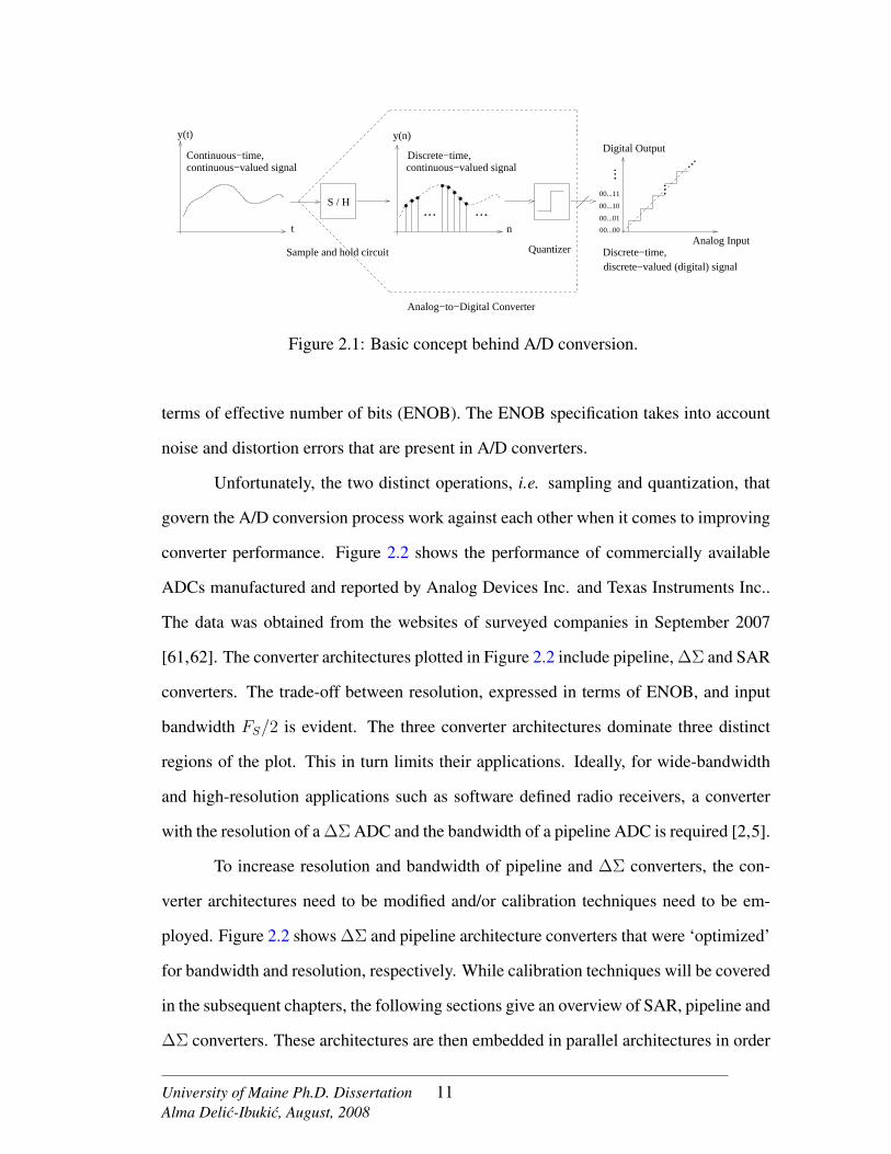
Unfortunately, the two distinct operations, i.e. sampling and quantization, that
govern the A/D conversion process work against each other when it comes to improving
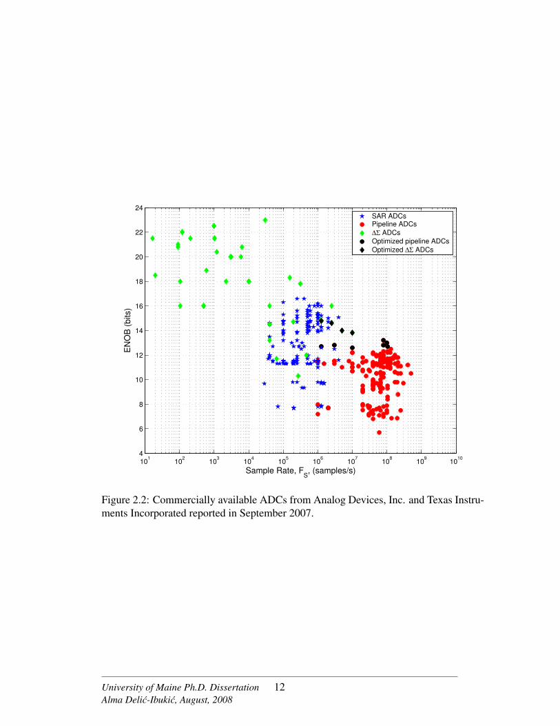
converter performance. Figure 2.2 shows the performance of commercially available
ADCs manufactured and reported by Analog Devices Inc. and Texas Instruments Inc..
The data was obtained from the websites of surveyed companies in September 2007
[61,62]. The converter architectures plotted in Figure 2.2 include pipeline, ∆Σ and SAR
converters. The trade-off between resolution, expressed in terms of ENOB, and input
bandwidth FS/2 is evident. The three converter architectures dominate three distinct
regions of the plot. This in turn limits their applications. Ideally, for wide-bandwidth
and high-resolution applications such as software defined radio receivers, a converter
with the resolution of a ∆Σ ADC and the bandwidth of a pipeline ADC is required [2,5].
To increase resolution and bandwidth of pipeline and ∆Σ converters, the con-
verter architectures need to be modified and/or calibration techniques need to be em-
ployed. Figure 2.2 shows ∆Σ and pipeline architecture converters that were ‘optimized’
for bandwidth and resolution, respectively. While calibration techniques will be covered
in the subsequent chapters, the following sections give an overview of SAR, pipeline and
∆Σ converters. These architectures are then embedded in parallel architectures in order
University of Maine Ph.D. DissertationAlma Delic-Ibukic, August, 2008
11
101 102 103 104 105 106 107 108 109 10104
6
8
10
12
14
16
18
20
22
24
Sample Rate, FS, (samples/s)
EN
OB
(bits
)
SAR ADCsPipeline ADCs∆Σ ADCsOptimized pipeline ADCsOptimized ∆Σ ADCs
Figure 2.2: Commercially available ADCs from Analog Devices, Inc. and Texas Instru-ments Incorporated reported in September 2007.
University of Maine Ph.D. DissertationAlma Delic-Ibukic, August, 2008
12
to increase the overall bandwidth and/or resolution of an ADC.
2.2 Successive-Approximation-Register (SAR) ADCs
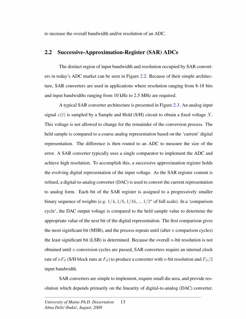
The distinct region of input bandwidth and resolution occupied by SAR convert-
ers in today’s ADC market can be seen in Figure 2.2. Because of their simple architec-
ture, SAR converters are used in applications where resolution ranging from 8-18 bits
and input bandwidths ranging from 10 kHz to 2.5 MHz are required.
A typical SAR converter architecture is presented in Figure 2.3. An analog input
signal x(t) is sampled by a Sample and Hold (S/H) circuit to obtain a fixed voltage X .
This voltage is not allowed to change for the remainder of the conversion process. The
held sample is compared to a coarse analog representation based on the ‘current’ digital
representation. The difference is then routed to an ADC to measure the size of the
error. A SAR converter typically uses a single comparator to implement the ADC and
achieve high resolution. To accomplish this, a successive approximation register holds
the evolving digital representation of the input voltage. As the SAR register content is
refined, a digital-to-analog converter (DAC) is used to convert the current representation
to analog form. Each bit of the SAR register is assigned to a progressively smaller
binary sequence of weights (e.g. 1/4, 1/8, 1/16, ... 1/2n of full scale). In a ‘comparison
cycle’, the DAC output voltage is compared to the held sample value to determine the
appropriate value of the next bit of the digital representation. The first comparison gives
the most significant bit (MSB), and the process repeats until (after n comparison cycles)
the least significant bit (LSB) is determined. Because the overall n-bit resolution is not
obtained until n conversion cycles are passed, SAR converters require an internal clock
rate of nFS (S/H block runs at FS) to produce a converter with n-bit resolution and FS/2
input bandwidth.
SAR converters are simple to implement, require small die area, and provide res-
olution which depends primarily on the linearity of digital-to-analog (DAC) converter.
University of Maine Ph.D. DissertationAlma Delic-Ibukic, August, 2008
13
ADC+
−
Successiveapproximationregister
S/H outputDigitalXx(t)
DAC
Figure 2.3: Successive-approximation-register A/D converter block diagram.
However, their use of oversampling limits them to low-bandwidth applications. For
wide-bandwidth applications, different converter architectures must be considered.
2.3 Pipeline Architecture ADCs
Pipeline architecture converters are well suited for wide-bandwidth applications
where the required resolutions range up to 12 bits. This is because the overall sampling
rate, FS , of a pipeline ADC is determined by the speed of a single low resolution stage.
Figure 2.4 illustrates a conventional pipeline converter architecture. The pipeline
converter consists of lower resolution stages that are pipelined together to work consec-
utively to form a high resolution output. Each stage in the pipeline serves two purposes:
to provide qi, a low resolution digital estimate of the input voltage and to provide the
next stage in the pipeline with the ‘residual’ ri (the difference between the input volt-
age and the digital estimate qi). Once all stages have processed the given input sample,
all qi’s are collected in a digital encoder block where they are properly recombined to
achieve a higher resolution representation of the analog input voltage X . Because the
digital output is not available until the last stage in the pipeline has processed the given
input sample, there is an inherent latency associated with a pipeline architectures. This
latency increases with the number of additional stages.
Figure 2.5 shows the block diagram of a typical pipeline low resolution stage.
The analog input signal ri−1 is sampled by the Sample and Hold (S/H) circuit. The
sampled input is converted to a coarse digital output of a stage by the low resolution
University of Maine Ph.D. DissertationAlma Delic-Ibukic, August, 2008
14

Stage 2 Stage N
qnq
1 q2
Stage 1
Digital Output
Xr1 2r
Clock
Digital Encoder
Figure 2.4: Generic pipeline ADC block diagram.
flash ADC (sub-ADC). The sub-ADC output qi is an integer value ranging from 0 to
2Bi − 1, where Bi is the number of resolvable bits for the given stage. Once the coarse
digital output is obtained, the value is passed on to the low resolution DAC (sub-DAC) to
form the analog equivalent of the coarse digital input sample. This voltage is subtracted
from the initial input sample giving the quantization error voltage, ei. The resulting
error voltage ei is scaled by the gain factor Gi and passed as a residual ri to the next
stage in the attempt to improve the digital representation of the input. The gain factor is
selected so the error voltage of the first stage doesn’t exceed the acceptable input range
of the next stage. For an ideal sub-ADC and sub-DAC, the gain factor can be selected
to be Gi = 2Bi . Selecting a gain factor as a power of two simplifies the logic of digital
encoder block.
For pipeline architecture converters, hardware complexity is directly propor-
tional to the number of bits resolved. Compared ot high resolution stages, low reso-
lution stages are easier to build and they occupy little real estate on silicon. In theory,
a pipeline converter with N -stages, where each stage contains a B-bit sub-ADC, will
produce a wide-bandwidth ADC with the overall resolution of n = NB bits using
University of Maine Ph.D. DissertationAlma Delic-Ibukic, August, 2008
15

Bi( −bit)qi
−bitBi −bitBi
ri−1Gi
DAC
+−
+S/H
ADC
riie
Figure 2.5: Generic pipeline stage block diagram.
N(2B − 1) comparators. For example, a 2 bits per stage architecture requires 3 com-
parators per stage and a 4 bits per stage architecture requires 15 comparators per stage.
At the same time, low-resolution stages require more pipeline stages to obtain higher
final ADC resolution and vice versa.
In theory, with a given per stage resolution, one can build a pipeline A/D con-
verter with any resolution by cascading the appropriate number of stages. However, in
practice, monolithic, high-resolution pipeline ADCs are difficult to obtain due to ex-
traordinary component matching requirements. Component matching becomes increas-
ingly difficult as CMOS technologies are scaled to smaller geometries. Error sources
encountered in pipeline architecture converters and ways to cope with them are dis-
cussed in Chapter 3.
2.4 Oversampled Converter Architectures
One way to improve the resolution of Nyquist rate converters (e.g., pipeline ar-
chitecture ADCs) is by employing oversampling. With oversampling, the analog input
signal is sampled at a sampling rate that is much higher than the Nyquist rate FS . To un-
derstand the benefits of oversampling, requires revisiting the quantization process. The
following sections provide an overview of quantization, oversampled A/D converters,
University of Maine Ph.D. DissertationAlma Delic-Ibukic, August, 2008
16

Vref2
−Vref2
Vref2
−Vref2
Vref
−Vref
Vref
−Vref
Ideal streight line
2−bit quantizer output
X
Vout
(a) Transfer characteristics of a uniform 2-bitquantizer.
Vref4
−Vref4
−Vref VrefX
e
(b) Quantization error for a 2-bit quantizer.
Figure 2.6: An example of a uniform 2-bit quantizer and quantization error e showingthe deviation of the actual 2-bit quantizer from the straight line (ideal quantizer).
and oversampled noise-shaping A/D converters.
2.4.1 Quantization
As mentioned in Section 2.1, to convert an analog signal into a digital signal,
two distinct operations need to take place: sampling and quantization. The quantization
process assigns a continuous valued input to one of a finite numbers of discrete (digital)
values as an output. A transfer characteristic of a 2-bit quantizer together with the ideal
straight line are shown in Figure 2.6(a). The ideal straight line represents a quantizer
with infinite resolution, meaning one-to-one correspondence between analog inputs and
their digital counterparts. The quantization interval (i.e., the distance between two con-
secutive quantization levels) is given by QB = 2VREF/2B, where B is resolution of a
quantizer and ±VREF is the input range of the quantizer. For the 2-bit quantizer illus-
trated in Figure 2.6(a), the quantization interval is given by Q2 = 2VREF/4 = VREF/2.
The difference between the quantizer output and the ideal straight line is known as quan-
tization error or quantization noise. The quantization error for an ideal 2-bit quantizer
is plotted in Figure 2.6(b). Because the quantizer with an infinite resolution doesn’t
University of Maine Ph.D. DissertationAlma Delic-Ibukic, August, 2008
17

exist, quantization error inherently exists in every A/D converter. As long as the quan-
tizer doesn’t saturate (|X| ≤ VREF ) the quantization error e for an ideal A/D con-
verter is bounded by ±QB/2. For the case of a 2-bit quantizer, this translates into
|e| ≤ Q2/2 = VREF/4.
Even though quantization error is fully dependant on the input signal X , as long
as the input signal is not constant or does not change regularly by multiples or submul-
tiples of the quantization interval QB between sample times, quantization error can be
modelled as an additive white noise process [13,63]. Modelling quantization error as an
additive white noise process with samples uniformly distributed within ±QB/2 interval
simplifies the analysis of A/D converters. The following sections discuss the benefits of
oversampling by utilizing a model of quantization error as an additive noise source.
2.4.2 Oversampled A/D Converter Architecture
Figure 2.7 shows an oversampled A/D converter architecture where the quan-
tizer is modelled as an additive noise source e. The input signal x(t) is sampled at a
rate D times higher than the Nyquist-rate, FS . Once the input signal is quantized the
high-rate digital output is low-pass filtered and decimated to obtain the digital output at
the Nyquist-rate. The factor D is known as the ‘oversampling ratio’ of the converter.
By employing oversampling, the resolution of the converter is increased because the
quantization noise is reduced within the signal band.
The total amount of the quantization noise power σ2e that is added to the sampled
signal is the same regardless of whether or not the input signal is oversampled. As-
suming that the quantization noise e is uniformly distributed over ±QB/2 interval, the
quantization noise power σ2e is given by
σ2e =
1
QB
∫ QB/2
−QB/2e2de = Q2
B/12. (2.1)
University of Maine Ph.D. DissertationAlma Delic-Ibukic, August, 2008
18

LPF D outputDigital
Digital decimation filter
e
S/H
ADC model
x(t)
quantizer
High speed clock (DFs)
sampler
Nyquist rate clock (Fs)
Figure 2.7: Oversampled A/D converter architecture.
Even though σ2e is the same regardless of whether oversampling is used, what differs
is the frequency distribution of the quantization noise power when oversampling is em-
ployed. Because oversampling requires sampling frequencies that are much higher than
Nyquist-rate frequencies, the same amount of quantization noise power is distributed
over a wider frequency range. This reduces the noise power in the frequency band of
interest, which in turn, increases the resolution of the converter. Figure 2.8 illustrates
this fact, where the quantization noise power frequency distribution is shown for an A/D
converter with and without oversampling. The signal band of interest is the region from
−FS/2 to FS/2. For the oversampled converter architectures there is an apparent quanti-
zation noise reduction in the desired region that contributes to the increase in converter’s
resolution.
2.4.3 ∆Σ Architecture ADCs
The resolution of oversampled converter architectures can be further improved
by integrating noise-shaping with oversampling. The most popular A/D converter ar-
chitecture that employs noise-shaping and oversampling are based on ∆Σ modulators.
These architectures are known as ∆Σ ADCs. Figure 2.2 shows the performance of ∆Σ
architecture converters. For a relatively small input bandwidths, resolutions up to 24-bits
are obtainable.
University of Maine Ph.D. DissertationAlma Delic-Ibukic, August, 2008
19

Se(f)
Nyquist-rate converters
Oversampled A/D converters
QB2
12FS
QB2
12( DFS )
f-D(FS /2) -FS /2 FS /2 D(FS /2)
Figure 2.8: Quantization noise power spectral density for A/D converters with and with-out oversampling employed.
LPF D
DAC
+
− outputDigital
Digital decimation filter
e
∆Σ
ADC
modulator
x[n]
Figure 2.9: ∆Σ converter architecture implemented using first order ∆Σ modulators.
University of Maine Ph.D. DissertationAlma Delic-Ibukic, August, 2008
20

+ −
x[n]
e[n]
y[n]−1
−1z
1−z
Figure 2.10: Linear model for a first order ∆Σ modulator.
Figure 2.9 shows a ∆Σ converter architecture implemented using a first order
∆Σ modulator. The ∆Σ modulator operates at a sampling speed that is much higher
than the digital output data rate FS , which determines the overall input bandwidth of the
converter (FS/2). The basic modulator components are: an integrator, a single compara-
tor (ADC), and a low-resolution DAC. The high data rate digital output coming from the
∆Σ modulator is lowpass filtered and downsampled to provide a final high-resolution,
low-bandwidth output. The use of an integrator with feedback forces that average value
of the quantizer output to track the average value of the input signal. Because averag-
ing occurs at sampling speeds that are much faster than the Nyquist-rate, the average
error between the quantized output and the input signal is reduced. This implies that
the quantization noise is pushed out of the signal band of interest to higher frequencies
where it is filtered out.
Figure 2.10 shows a linear model of a first order ∆Σ modulator. The linear
model simplifies the behavioral analysis of the ∆Σ modulator. Using the z-transform
the output y[n] in Figure 2.10 is given by
Y (z) = X(z)z−1 + E(z)(1− z−1)
= X(z)STF (z) + E(z)NTF (z) (2.2)
In this equation, STF (z) = z−1 represents the signal transfer function that delays the
input signal x[n], and NTF (z) = (1 − z−1) represents the noise transfer function that
University of Maine Ph.D. DissertationAlma Delic-Ibukic, August, 2008
21

0 0.05 0.1 0.15 0.2 0.25 0.3 0.35 0.4 0.45 0.50
0.2
0.4
0.6
0.8
1
1.2
1.4
1.6
1.8
2
Mag
nitu
de
Normilized frequency
NTF(z) = 1 − z−1
STF(z) = z−1Des
ired
sign
al b
andw
idth
Figure 2.11: Frequency response of NTF (z) and STF (z) for the first order ∆Σ mod-ulator. The normalized frequency is given by f = F
DFS, where FS is the Nyquist-rate
frequency for the first order ∆Σ modulator and D is the oversampling ratio.
only affects the quantization noise e[n]. Figure 2.11 shows the frequency response of
noise transfer function NTF (z) and signal transfer function STF (z) for a first order
∆Σ modulator. Attenuation of the quantization noise in the signal band of interest by
NTF (z) is evident. The low frequency quantization noise is moved to higher frequen-
cies and outside the band of interest. In general, an Lth order ∆Σ modulator can be
modelled by
Y (z) = X(z)z−m + E(z)(1− z−1)L
= X(z)STF (z) + E(z)NTF (z) (2.3)
where STF (z) = z−m is a signal transfer function that delays the input signal by m
samples, and NTF (z) = (1 − z−1)L is a noise transfer function that contributes to
minimization of the quantization noise within the signal band [13].
From Figure 2.9, the lowpass filter that follows the ∆Σ modulator is designed to
University of Maine Ph.D. DissertationAlma Delic-Ibukic, August, 2008
22

remove as much of the out-of-band quantization noise as possible. Otherwise, following
the decimation (i.e., reducing the sampling rate down to Nyquist-rate) the quantization
noise at frequencies that are a multiple of the oversampling ratio will fold back into a
signal band of interest. It is common to implement the decimation filter for ∆Σ converter
architectures by cascading comb filters [13, 63], where each comb filter stage has the
transfer function1
D
(1− z−D
1− z−1
). In general, for the Lth order ∆Σ modulator, L + 1
comb filters are cascaded to sufficiently reduce the out-of-band quantization noise [13].
For a first order modulator, a two stage comb filter is used as the decimation filter, having
the transfer function
G(z) =1
D2
(1− z−D
1− z−1
)2
(2.4)
and associated frequency response given by
G(ej2πf ) =1
D2
(sin(Dπf)
sin(πf)
)2
(2.5)
From (2.4) it can be observed that the filter has periodically spaced zeros on the unit cir-
cle at z = ej2πkD for k = 1, 2, 3, ...D−1. Figure 2.12 shows the frequency response of the
two stage comb filter with D = 20. The lowpass characteristic with periodically spaced
zeros at 1/D and its multiples can be observed. The lowpass filter portion preserves the
desired input signal band and periodically spaced zeros make sure that the out-of-band
quantization noise is attenuated sufficiently so that only a small portion appears back in
the signal band.
∆Σ converter architectures require primarily digital circuitry, and when com-
pared to pipeline converters, they don’t rely on high precision analog components [13,
63]. The drawback of ∆Σ converters is the need for a high oversampling ratio D to
get high linearity for relatively small input bandwidth. To maintain high linearity that
∆Σ converters offer and increase the bandwidth of the converter, ∆Σ modulators can be
placed in parallel [16,64]. Parallel architecture converters are discussed in the following
University of Maine Ph.D. DissertationAlma Delic-Ibukic, August, 2008
23
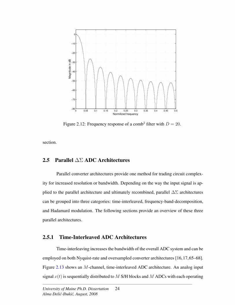
0 0.05 0.1 0.15 0.2 0.25 0.3 0.35 0.4 0.45 0.5−80
−70
−60
−50
−40
−30
−20
−10
0
Normilized frequency
Mag
nitu
de in
dB
Figure 2.12: Frequency response of a comb2 filter with D = 20.
section.
2.5 Parallel ∆Σ ADC Architectures
Parallel converter architectures provide one method for trading circuit complex-
ity for increased resolution or bandwidth. Depending on the way the input signal is ap-
plied to the parallel architecture and ultimately recombined, parallel ∆Σ architectures
can be grouped into three categories: time-interleaved, frequency-band-decomposition,
and Hadamard modulation. The following sections provide an overview of these three
parallel architectures.
2.5.1 Time-Interleaved ADC Architectures
Time-interleaving increases the bandwidth of the overall ADC system and can be
employed on both Nyquist-rate and oversampled converter architectures [16,17,65–68].
Figure 2.13 shows an M -channel, time-interleaved ADC architecture. An analog input
signal x(t) is sequentially distributed toM S/H blocks andM ADCs with each operating
University of Maine Ph.D. DissertationAlma Delic-Ibukic, August, 2008
24

S/Hn bits
ADC 1
S/Hn bits
S/Hn bits
FS
M
n bits
ADC M
ADC 2
Dig
ital M
ultip
lexe
r
Analog Demultiplexer
x(t)
Figure 2.13: An M -channel time-interleaved ADC system.
at 1/M of the overall system sample rate FS . Each channel operates at a different clock
phase, thereby allowing the final, high sample rate output to be formed by interleaving
the lower sample rate outputs of each channel in proper sequence (i.e. 1, 2, 3, ..., M, 1,
2, ...). This channel recombination occurs in the digital domain.
Besides having performance limitations due to the ADC architecture used, per-
formance of parallel architecture ADC systems is also limited by mismatches among
the channels. In addition to the gain and offset channel mismatch errors, the other com-
mon mismatch error for time-interleaved ADC systems is due to clock skew [69–71].
Clock skew errors cause sample time mismatches across channels [66,71,72]. One way
to avoid clock skew error is by implementing a front-end sample and hold (S/H) cir-
cuit [66]. Figure 2.14 shows the modifiedM -channel time-interleaved ADC system that
utilizes the front-end S/H circuit to minimize the clock skew errors. Here, the analog
input signal x(t) is first sampled at high sample rate and than sequentially distributed to
M ADCs with each operating at 1/M of the overall sample rate FS . This architecture
modification calls for a design of a S/H block that runs at M × FS sample rate.
University of Maine Ph.D. DissertationAlma Delic-Ibukic, August, 2008
25

n bits
n bits
n bits
n bitsADC 1
FS
M
Analog Demultiplexer
FS
S/H
ADC M
ADC 2
Dig
ital M
ultip
lexe
r
x(t)
Figure 2.14: Modified M -channel time-interleaved ADC system that avoids clock skewerrors.
2.5.2 Frequency-Band-Decomposition ADC Architecture
The frequency-band-decomposition ADC architecture is based on the concept of
filter banks [14, 15, 73–75] as illustrated in Figure 2.15. Two filter banks are required
to process the given input signal x[n], namely the analysis filter bank and synthesis
filter bank. The analysis filter bank Hk(z) breaks the wide bandwidth input signal x[n]
into M smaller frequency bands. Each frequency band is assigned to an A/D converter
processes the assigned band of frequencies (i.e. bandpass ADC). Because only 1/M th of
the input signal is being processed by a give channel, the sampling rate for each channel
is reduced by M . The synthesis filter bank Fk(z) takes the M frequency bands and
combines them back to the single frequency band of the original input signal x[n]. Once
all channels are recombined, the overall frequency response seen by x[n] is all-pass.
Figure 2.16 shows the frequency response for the bank of M analysis filters. Each filter
Hk(z), where k = 1, 2, ...,M is assigned a different frequency band so each channel
processes only 1/M th of the overall signal band.
Unlike time-interleaved converters, the frequency-band-decomposition ADC ar-
University of Maine Ph.D. DissertationAlma Delic-Ibukic, August, 2008
26
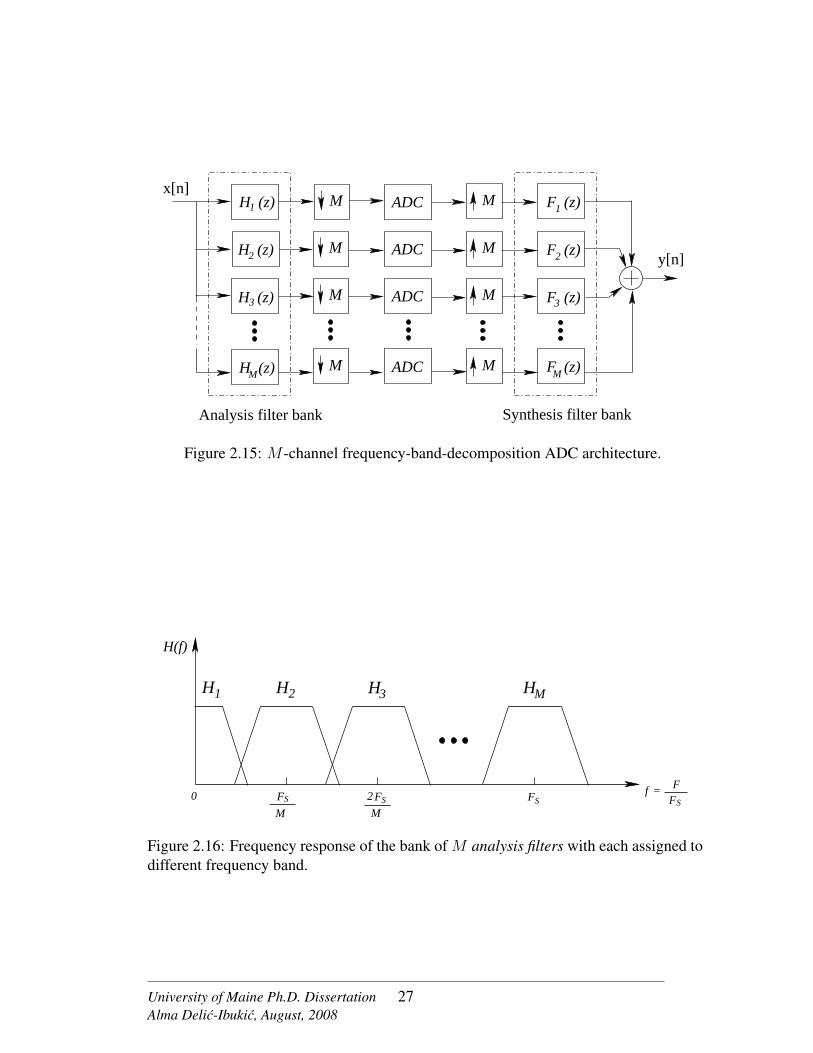
M
M
M
M
ADC
ADC
ADC
ADC
M
M
M
M
1F (z)H (z)
H (z)2
3
H (z)
1
H (z)
M
2F (z)
F (z)
F (z)M
3
Synthesis filter bankAnalysis filter bank
x[n]
y[n]
Figure 2.15: M -channel frequency-band-decomposition ADC architecture.
H2 H3 HMH1
H(f)
f =FS
M
F2 S
M
FS
FFS
0
Figure 2.16: Frequency response of the bank of M analysis filters with each assigned todifferent frequency band.
University of Maine Ph.D. DissertationAlma Delic-Ibukic, August, 2008
27

D
D
D
D
DG(z)
G(z)
G(z)
G(z)
G(z)
Ms [n]
M−1s [n]
1
2
3
x[n]
y[n]
s [n]
s [n]
s [n]
∆ Σ
∆ Σ
∆ Σ
∆ Σ
∆ Σ
1
2
3
M−1
M
p [n]
p [n]
p [n]
p [n]
p [n]
Figure 2.17: Π∆Σ A/D converter architecture.
chitecture is insensitive to channel mismatches [20,74]. On the other hand, each channel
of the frequency-band-decomposition architecture is unique, requiring a different filter
and bandpass A/D converter in each channel. This results in a complex design which is
more pronounced at the front end of the architecture where the analog components are
required (i.e. analysis filter bank) [14, 75].
2.5.3 Hadamard Modulated ∆Σ ADC Architecture
Parallel ∆Σ architectures implemented using Hadamard modulation are also
known as Π∆Σ ADCs [18, 19]. Hadamard modulated ∆Σ ADC architectures were
first reported in [18,64] as a method of implementing Nyquist rate converters. Later the
concept of ∆Σ channels operating in parallel without time-interleaving was extended to
oversampling converters which allows not just for the significant increase in the overall
converter bandwidth but also the increase in the overall converter resolution [19].
Figure 2.17 shows the oversampling Π∆Σ ADC architecture. The oversampling
University of Maine Ph.D. DissertationAlma Delic-Ibukic, August, 2008
28

ratio D does not depend on the number of channels used. The M parallel channels
have an input sequence x[n] applied simultaneously. Each channel is modulated by a
distinct ±1 sequence sr[n]. The ±1 sequences are selected as orthogonal Hadamard
sequences. An identical, but delayed and downsampled, copy of this signal pr[n] is
later used to (digitally) demodulate the channel. The remainder of the channels consist
of a conventional ∆Σ converter. However, the bandwidth of the lowpass filter G(z) is
significantly narrower than that of a conventional ∆Σ converter.
Aside from the selected modulation sequence, all Π∆Σ channels are identical.
Valid Hadamard sequences are available when M is a power of 2, placing a signifi-
cant restriction on the number of channels used for this architecture. Also (as for the
time-interleaved converters) Π∆Σ converters are sensitive to channel gain and offset
mismatches and Hadamard modulation level errors [19, 20, 30].
University of Maine Ph.D. DissertationAlma Delic-Ibukic, August, 2008
29

CHAPTER 3
Pipeline A/D Converter Calibration Techniques
This chapter provides an overview of pipeline architecture A/D converters using
1-bit per stage topology. Error mechanisms that can be present in a pipeline converter
are reviewed. Also, and different calibration techniques applicable to pipeline ADCs
are discussed. Also, a new real-time calibration technique based on the algorithm first
reported by Karanicolas et. al. in [28] will be introduced and its implementation in real-
time using Verilog HDL will be discussed. Calibration is successfully demonstrated
using a 14-bit ADC with 1-bit per stage architecture and 16 identical stages. More
detailed work behind the proposed real-time calibration scheme can be found in [57].
3.1 Pipeline Architecture Overview (1-bit per stage example)
High speed, high resolution, low power ADCs are frequently based on a pipeline
architecture because the overall speed of the pipeline converter is given by the speed of
the single low resolution stage.
Figure 3.1 shows a conventional 1-bit per stage pipeline converter architecture.
Each stage in the pipeline serves two purposes: to provide qi, the coarse resolution dig-
ital representation of the input voltage, and to provide the next stage in the pipeline
with ri, the difference between the input voltage and analog form of qi. This resid-
ual voltage, ri, is passed on to the subsequent stages for quantization in an attempt
to improve the digital representation of the input. All qi’s are collected in the digital
encoder block where they are combined properly to achieve a higher resolution rep-
resentation of the input voltage X . A pipeline stage consists of a sample and hold
(S/H) block, 1-bit analog-to-digital converter (sub-ADC), 1-bit digital-to-analog con-
verter (sub-DAC), analog subtractor and a gain block. The quantization interval for
a single 1-bit stage is Q = 2VREF/2 or just VREF . The sub-ADC for this particular
University of Maine Ph.D. DissertationAlma Delic-Ibukic, August, 2008
30

Stage 2 Stage N
qnq
1 q2
Stage 1
Digital Output
Xr1 2r
Clock
Digital Encoder
2
DAC
+−
+S/HX
ADC
r
q( )VREFsub sub
q
e
1
G1 11
1
1
Figure 3.1: Generic Pipeline ADC block diagram showing the details of a pipeline stage.
topology requires one comparator with a zero volt threshold. There are two valid digital
outputs of the sub-ADC block, a 0 or 1. The corresponding sub-DAC outputs for these
two digital values are −VREF/2 and +VREF/2. The sub-DAC outputs are subtracted
from the input and multiplied by the appropriate gain G. Ideally the gain should scale
the residual error to |ri| ≤ VREF , the input range of the subsequent stage. The input volt-
age X can be represented in terms of the error voltage, e, and sub-DAC outputs. The
representation of X in terms of the first stage error voltage, e1, and sub-DAC output, q1,
is
X = e1 +
(q1 −
1
2
)VREF (3.1)
The first stage residual voltage, r1, can be written in terms of the corresponding values
from the next stage in the pipeline.
r1 = G1e1 = e2 +
(q2 −
1
2
)VREF (3.2)
University of Maine Ph.D. DissertationAlma Delic-Ibukic, August, 2008
31

Solving (3.2) for e1 and making a substitution in (3.1) gives the input voltage, X , in
terms of the quantized outputs of the first two pipeline stages.
X =e2
G1
+
(q1 −
1
2
)VREF +
(q2 −
1
2
)VREFG1
(3.3)
The error voltage e2 is, in turn, amplified and quantized by Stage 3, refining the repre-
sentation of X .
X =e3
G1G2
+
(q1 −
1
2
)VREF +
(q2 −
1
2
)VREFG1
+
(q3 −
1
2
)VREFG1G2
(3.4)
This process continues throughout the remaining stages of the pipeline. For the N -stage
converter, the input voltage X is represented in terms of the quantized outputs of the N
stages and the error voltage eN as
X =eN
G1G2G3 . . . GN−1
+
(q1 −
1
2
)VREF +
(q2 −
1
2
)VREFG1
+
(q3 −
1
2
)VREFG1G2
. . .+
(qN−1 −
1
2
)VREF
G1G2G3 . . . GN−2
+
(qN −
1
2
)VREF
G1G2G3 . . . GN−1
(3.5)
Equation 3.5 contains all required terms to form the digital output code for this N -stage
converter. The digital output is given by:
D = q1 (G1G2G3 . . . GN−1) + q2 (G2G3G4 . . . GN−1) + q3 (G3G4G5 . . . GN−1)
+ . . . qN−2 (GN−2GN−1) + qN−1GN−1 + qN (3.6)
Often, pipeline ADCs are designed using identical stages. If the N -stage converter was
designed using N identical stages the digital output could be re-written as:
D = q1GN−1 + q2G
N−2 + q3GN−3 + . . . qN−2G
2 + qN−1G+ qN (3.7)
University of Maine Ph.D. DissertationAlma Delic-Ibukic, August, 2008
32

The digital output is correct as long as there are no gain errors in the pipeline.
3.2 Sources of Error in Pipeline A/D Converters
Figure 3.2 shows the residual characteristics for 1-bit ideal pipeline stage and
pipeline stage with sub-ADC, sub-DAC and interstage gain errors. Sub-ADC error can
be fixed by modifying a pipeline stage. Sub-DAC and interstage gain errors cannot be
fixed by implementing stage modifications alone. Rather, new techniques are required
to address these errors.
3.2.1 Sub-ADC Error
Variations in threshold voltages introduce a comparator offset error. Figure 3.2(a)
illustrates a residual error plot for a 1-bit ideal pipeline stage and a stage with compara-
tor offset error. This error characteristic causes the residual output of one stage to exceed
the input range of the next stage.
There are two ways to relax the comparator offset requirements: increase the
quantization resolution of the stage and keep the interstage gain as a power of two, or
keep the same number of bits per stage but reduce the interstage gain. Increasing the
quantization interval of the stage allows for the digital encoder block to remain the same,
because the interstage gain does not change. On the other hand, reducing the interstage
gain adds complexity to the digital encoder block design.
When implementing the digital calibration, values used to form the ADC out-
put code need to be modified. This requires alteration of the digital encoder block. If
modification of the digital encoder is needed, then reducing the gain of the stage is the
better choice for dealing with the comparator offset errors. The interstage gain reduction
generally requires additional stages so that the resolution of the converter is not com-
promised. Equation 3.7 provides a means for determining the relationship between the
implemented value of G and the number of required stages. For example, to obtain a
University of Maine Ph.D. DissertationAlma Delic-Ibukic, August, 2008
33

−V
RE
F
+V
RE
F
−VREF
+VREF
Vou
t
Vin
q = 0 q = 1
(a) comparator offset (sub-ADC error)
−V
RE
F
+V
RE
F
−VREF
+VREF
Vou
t
Vin
(b) charge injection (sub-DAC error)
−V
RE
F
+V
RE
F
−VREF
+VREF
Vou
t
Vin
(c) capacitor mismatch (gain error)
Figure 3.2: Residual error plots for 1-bit per stage ideal pipeline ADC (blue) andpipeline ADC with errors (red).
University of Maine Ph.D. DissertationAlma Delic-Ibukic, August, 2008
34

converter with a 14-bit resolution, we set D = 214−1 for all qi = 1. Using N = 16 stages
gives a value of G = 1.81, small enough to ensure that residual voltages will not saturate
subsequent stages.
If the interstage gain is less than two, the full scale voltage (VFS) of the pipeline
is no longer ±VREF . The full scale voltage for a converter with an arbitrary gain can be
derived by solving for the input voltage VFS that produces residual voltage VFS at each
stage of the pipeline. The following relationship between the interstage gain, G, and full
scale voltage, VFS , is derived:
G(VFS − VDAC) = VFS, where VDAC =VREF
2.
VFS =G
G− 1
(VREF
2
)(3.8)
The new quantization interval is now given by Q = 2VFS/2n, where n is the number of
bits.
Reducing an interstage gain allows for variations in threshold voltages of the
sub-ADC comparators. Figure 3.3 shows the residual error characteristics for the 1-bit
per stage architecture and allowed threshold voltage change (∆VADC) before the full
scale range of the next stage is reached. The allowed variations in a threshold voltage of
a sub-ADC comparator for a converter with the arbitrary gain is given by:
∆VADC = ±VREF2
(1
G− 1− 1
)(3.9)
For the 14-bit, 16 stage example introduced above, the gain of 1.81 is used and VREF
is set to 1V. The full scale range of the converter is VFS = 1.12 V. This accommodates
±0.12 V variations in the threshold voltage of the sub-ADC comparator.
University of Maine Ph.D. DissertationAlma Delic-Ibukic, August, 2008
35
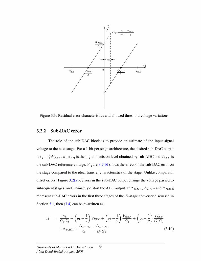
Vin
−VREF +VREF
Vou
t
−VREF
2
+VREF
2
VREF
2
G
V∆ ADC
VFSG
G−1
VREF
2
0
=
Figure 3.3: Residual error characteristics and allowed threshold voltage variations.
3.2.2 Sub-DAC error
The role of the sub-DAC block is to provide an estimate of the input signal
voltage to the next stage. For a 1-bit per stage architecture, the desired sub-DAC output
is (q − 12)VREF , where q is the digital decision level obtained by sub-ADC and VREF is
the sub-DAC reference voltage. Figure 3.2(b) shows the effect of the sub-DAC error on
the stage compared to the ideal transfer characteristics of the stage. Unlike comparator
offset errors (Figure 3.2(a)), errors in the sub-DAC output change the voltage passed to
subsequent stages, and ultimately distort the ADC output. If ∆DAC1, ∆DAC2 and ∆DAC3
represent sub-DAC errors in the first three stages of the N -stage converter discussed in
Section 3.1, then (3.4) can be re-written as
X =e3
G1G2
+
(q1 −
1
2
)VREF +
(q2 −
1
2
)VREFG1
+
(q3 −
1
2
)VREFG1G2
+∆DAC1 +∆DAC2
G1
+∆DAC3
G1G2
(3.10)
University of Maine Ph.D. DissertationAlma Delic-Ibukic, August, 2008
36

Vin
V+ DAC
Voutq
φ
φ
φ2
1φ1
2
C1
C2
VDAC−
+
−
Figure 3.4: Switched capacitor implementation of the MDAC for 1-bit per stage archi-tecture.
From (3.10) it can be seen that the sub-DAC error associated with a stage scales down
by the total gain factor of all previous stages. Stages near the pipeline front end are
especially critical, and tend to dominate these error contributions.
3.2.3 Interstage Gain Error
Figure 3.2(c) shows the gain error effect compared to the ideal transfer character-
istics of the stage. The gain error changes the slope of the residual curve. Many modern
pipeline converters are implemented using switched capacitor circuits [47]. This tech-
nology is suitable for high-speed, low power and monolithic CMOS implementations of
pipeline ADCs. For CMOS implementations, the S/H block, sub-DAC and gain block
are implemented together in what is known as a multiplying digital-to-analog converter
(MDAC). Figure 3.4 shows switched capacitor implementation of the MDAC for 1-bit
per stage architecture. Non-overlapping clocks, φ1 and φ2, control the switches of the
MDAC. During φ1, the input voltage is sampled onto two capacitors, C1 and C2. During
φ2, C2 is connected to the amplifier through the feedback loop and C1 is sampling one
University of Maine Ph.D. DissertationAlma Delic-Ibukic, August, 2008
37

of the sub-DAC outputs, q or q. The output of the MDAC can be written as
Vout =
(1 +
C1
C2
)Vin −
C1
C2
VDAC , (3.11)
where VDAC can be either +VDAC or −VDAC , depending on the sub-ADC output q.
From (3.11) it can be seen that the two capacitors in the MDAC block determine the
value of gain. If there is a mismatch in one of the capacitor values, C1 + ∆C1 instead of
C1, the gain would be altered as
Vout =
(1 +
C1
C2
+∆C1
C2
)Vin −
(C1
C2
+∆C1
C2
)VDAC . (3.12)
If a gain of 2 is desired, the two capacitors, C1 and C2, need to be perfectly
matched. Equation 3.6 shows dependency of the ADC output on gains. When design-
ing the digital encoder block, gains are known in advance and their digital representa-
tions are implemented in hardware to be used during normal converter operation. When
there is a gain error in a pipeline converter, the ADC output is greatly affected because
the digital encoder assumes the nominal gain. For accurate representation of any gain
value, excellent capacitor matching is required. In current process technologies, ca-
pacitor matching of ±0.1% is achievable. This process limitation limits the achievable
resolution of pipeline ADCs to roughly 10 bits. For higher resolution converters some
form of calibration must be employed.
3.3 Analog Calibration Schemes
Analog calibration schemes use the analog signal path and extra analog circuitry
to apply corrections to the stage being calibrated [21, 34–36]. The idea behind analog
calibration is to estimate dominant stage errors and then adjust required voltages and
gains back to their nominal values. These techniques adjust the threshold voltage of
University of Maine Ph.D. DissertationAlma Delic-Ibukic, August, 2008
38
the sub-ADC, reference voltage of the sub-DAC, and capacitor values of the gain block
while the digital encoder block remains unchanged.
Lin et al. [36] have used the digital output to correct for the gain errors of the
converter by adjusting values of the sampling capacitors in the MDAC. This was accom-
plished by attaching small trim capacitors to the sampling capacitor. Through iteration,
the best capacitor configuration is found. To obtain sufficient resolution trim capacitors,
a capacitor divider array was implemented. This technique is complicated by the exis-
tence of parasitic capacitances. For optimal trim capacitors, all capacitances, including
parasitics, need to be included in the calculation of the final capacitance. This calibra-
tion technique takes place during the power up of the converter or any time the converter
is idle. While the converter is re-calibrating, normal operation is suspended. Any envi-
ronmental changes, or changes in power supply voltage during normal operation of the
converter can affect the performance of the converter and will not be accounted for with
this calibration process.
A continuous calibration time technique in the analog domain has been reported
in the literature [21, 35]. Ingino et al. [21] employed an additional pipeline stage that
replaces the pipeline stage being calibrated. In this way, the normal operation of the
converter is not interrupted. The calibration technique uses the analog signal path to
adjust each stage’s reference voltage and comparator threshold voltage to meet the input
range requirement of subsequent stages. Adjustments are determined using a successive
approximation algorithm. Ming et al. [35] proposed a statistically based background
calibration scheme where the sub-DAC reference voltages are adjusted to correct for the
interstage gain error. During normal operation of the converter, the calibration signal is
added to the input and both are processed simultaneously. Adding two signals together
may cause saturation of the subsequent stage. To avoid this, special consideration needs
to be given to the design of the sub-ADC comparators.
Analog calibration techniques are favorable because the overall power consump-
University of Maine Ph.D. DissertationAlma Delic-Ibukic, August, 2008
39

tion of the converter stays low and the digital encoder block is not affected by the cal-
ibration process. However, as mentioned before, most of today’s pipeline ADCs are
designed using switched capacitor circuits. With scaled technologies, analog switch ca-
pacitor components are becoming more difficult to design. This is due to the increase in
sub-threshold and gate leakage currents and reduced power supply voltage [47]. Sam-
pling capacitors of the MDAC depend on accurately holding the signal value, e, to within
|e| < Q/2, if the residual is to be within the input range of the next stage. In this case,
the subsequent stages will be able to correct the error. Any sub-threshold and gate leak-
age currents will introduce a voltage error that translates to sub-DAC and gain errors.
To better fit scaled technology, a fully digital calibration schemes are considered next.
3.4 Digital Calibration Schemes
Digital calibration schemes measure error contributions in the digital domain.
The measured gain and reference voltage deviations are not adjusted back to their nom-
inal values, but rather they used to form the ADC output code [28, 42, 43, 76]. Equation
3.5 shows the dependency of the ADC output on the sub-DAC reference voltages and
interstage gains. The accuracy of the calibration depends on how well the errors are
measured in the digital domain. To digitally correct the ADC output code, extra digital
circuitry is required in the digital encoder block.
Lee and Song [76] measured dislocation of the digital output code from the ideal
transfer curve. In their work, the dislocation, defined as code errors, were measured
during the calibration cycle and stored in memory. Later on, during the normal oper-
ation of the converter, these code errors are recalled and subtracted digitally from the
uncalibrated digital outputs of the converter. Karanicolas et al. [28] looked at the residue
characteristics of the stage at the comparator threshold input voltage. Each segment of
the residue plot corresponds to different digital output of the stage. For the same input
voltage the residual of a given stage can come from either line segment. The idea behind
University of Maine Ph.D. DissertationAlma Delic-Ibukic, August, 2008
40

the calibration algorithm derived by Karanicolas et al. [28] is to ensure that for the same
input voltage the digital output remains unchanged regardless of which segment is cho-
sen by the comparator of a given stage. This calibration technique corrects for capacitor
mismatch, charge injection, comparator offset and finite op-amp gain.
The calibration techniques mentioned above rely on a fully digital implementa-
tion. However, both schemes are foreground calibration strategies. They are conducted
on converter power up. If re-calibration is required, the normal converter operation must
be interrupted.
Background or continuous digital calibration schemes have been reported in the
literature [42, 43]. Shu et al. [42] measured DAC errors in the background using a real-
time oversampling calibrator that was implemented using an oversampling delta-sigma
converter. This calibration technique does not account for gain errors resulting from
capacitor mismatch. Another continuous digital calibration technique was employed
by Moon et al. [43]. Their proposed technique is based on the concept of skipping a
conversion cycle randomly to free a clock cycle for calibration purposes. The skipped
sample is filled in later using nonlinear interpolation. Because of the finite resolution of
the data samples on which the nonlinear interpolation is applied, the interpolated value
suffers from uncertainty that affects the final resolution of the converter.
All the continuous digital calibration schemes discussed above have limitations.
They do not correct for all errors of a pipeline stage [42]. Accurate interpolation of
skipped samples is difficult to realize and results in distortion of the ADC output se-
quence [43]. The following sections describe an off-line digital calibration scheme de-
veloped by Karanicolas et al. [28] and subsequently demonstrate needed adaptations for
it to work in a continuous calibration mode.
University of Maine Ph.D. DissertationAlma Delic-Ibukic, August, 2008
41

DS2ω 7
q7 = 0 to find S1
= 1 to find Sq7 2
STAGES 8 −−> 16
G < 2
STAGE 7
G < 2
VoutVin6r
9
−DS1=
Set
Set
Digital encoder andcalibration logic block
Digital ADC Output
(a) Off-line digital calibration applied to the seventh stage.
Vin
Vou
t
+V REF
−VREF
−V
RE
F
+V
RE
F
S 1
S 2q = 0 q = 1
0
(b) Residual error plot of 1-bit per stage architecture with errors.
Figure 3.5: Pipeline ADC with off-line digital calibration applied to the seventh stage.
University of Maine Ph.D. DissertationAlma Delic-Ibukic, August, 2008
42
3.4.1 Off-line Calibration
Figure 3.5 illustrates the foreground calibration process derived in [28] for a
single stage of a pipeline ADC. The illustrated case is based on the implementation
of a 14-bit ADC with 16 identical stages, interstage gains less than two, and 1-bit per
stage topology. Gains less than two are chosen for all 16 stages so the output of each
stage does not saturate the remaining stages. Calibration begins with the least signifi-
cant stages (the end of the pipeline) and progresses toward the most significant stages.
For example, to calibrate stage 7, we must assume that stages 8-16 have already been
calibrated, or have been fabricated to sufficient accuracy that calibration is not needed.
Figure 3.5(a) shows the off-line digital calibration applied to the seventh stage of a
16-stage architecture. Figure 3.5(b) shows residual characteristics for the stage being
calibrated. Following calibration of the seventh stage, the process continues with the
sixth stage, and so on until the first stage is reached and the calibration of the converter
is complete.
Equation 3.6, derived in Section 3.1, describes the digital output of the N -stage
converter. Bit seen at the output of each stage is given a weight indicated by the gain
products given in parenthesis. Most pipeline ADCs use ‘nominal’ design gains to con-
struct the digital output. This approach is correct only if the converter is free of any
gain or sub-DAC errors. If the implemented gain is different from the design value, or
if sub-DAC errors exist, there will be error in the ADC output. Making these weights
programmable is the idea behind most of digital calibration techniques. This is the case
for the calibration algorithm derived by Karanicolas et al., where the correction terms
ωi are programmable and are updated each time a stage is calibrated. Equation 3.6 can
be re-written in terms of these weights,
D =N∑i=1
qiωi, (3.13)
University of Maine Ph.D. DissertationAlma Delic-Ibukic, August, 2008
43

where qi is the output bit for stage i and N is the number of stages used.
Pipeline converter error characteristics often show discontinuities associated with
the change in the output of the sub-ADC comparators. The residual error shown in Fig-
ure 3.5(b) consists of two segments (for q=0 and q=1) and the transition between the
segments is determined by the comparator threshold. The goal of digital calibration is
to ensure that for the same input voltage, the digital ADC output remains unchanged
regardless of which segment is selected by the sub-ADC comparator of the stage. To
assure this consistency, the converter output is examined for a stage input set to zero
volts, where the stage is forced to operate on each of the segments. Setting q7=0 with
Vin=0, forces Stage 7 to operate on the left segment, producing output residual voltage
S1. S1 is quantized by the remaining pipeline stages (stages 8, 9, 10,..., 16), producing
digital output DS1 . When Stage 7 is added to the pipeline, the resulting digital output is
given by
q7ω7|q7=0 +DS1 = DS1 (3.14)
Setting q7=1 (Vin=0) forces Stage 7 to operate on the right segment, producing residual
voltage S2. S2 is quantized by the remaining pipeline stages to give a digital outputDS2 .
The pipeline output in this case is
q7ω7|q7=1 +DS2 = ω7 +DS2 (3.15)
For a consistent digital output, ω7 should be selected so (3.14) and (3.15) agree. Setting
(3.14) and (3.15) equal to each other gives the expression for ω7.
ω7 = DS1 −DS2 (3.16)
The residual voltage terms S1 and S2 for a single stage are identified in Fig-
ure 3.5(b). Once the digital representations DS1 and DS2 for the residual voltages S1
University of Maine Ph.D. DissertationAlma Delic-Ibukic, August, 2008
44

1φ
2φ
Figure 3.6: Example of a two-phase, non-overlapping clock signal used in pipeline ADCarchitecture.
and S2 are found, the correction term ωi can be obtained. The correction term ωi is fed
back to the digital encoder and calibration logic block. This value is a weight associ-
ated with the bit of the stage being calibrated and it carries the information about the
interstage gain and sub-DAC errors.
The off-line calibration algorithm discussed above states that the correction terms,
ωi’s, can be found for all pipeline stages starting with the least significant stage and
progressing towards the most significant stage. In practice, calibration of the least sig-
nificant stages is not required since the converter error is dominated by the first few
stages of the pipeline. Current process technology easily accomplishes 8-bit accuracy
without calibration, suggesting that the last 7 stages (1 bit/stage topology) need not be
calibrated. Simulations have verified this, and suggest that starting calibration at the
least significant stages may actually degrade performance [57].
3.4.2 Real-Time Digital Calibration Scheme Development
Pipeline architecture ADCs rely on the two-phase, non-overlapping clock sig-
nal shown in Figure 3.6. All the odd stages in a pipeline sample during phase φ1 and
present the valid residue output to the next stage during φ2. All the even stages work
on the opposite clock phase. This allows for all stages in the pipeline to operate concur-
University of Maine Ph.D. DissertationAlma Delic-Ibukic, August, 2008
45

rently. A proposed real-time digital calibration based on the algorithm derived in [28]
was realized using two extra stages located at the end of the pipeline. These two extra
stages are active only during calibration. Two extra stages at the end of the pipeline
allow for a calibration sample to be introduced in the pipeline and still maintain the
normal operation of the converter. Table 3.1 shows propagation of samples through the
pipeline during the calibration process. Table 3.1 is based on a 14-bit ADC with 1-bit
per stage topology, 16 identical stages plus two additional stages for calibration (total of
18 pipeline stages), and gains less than two. Numbers 1 through 18 indicate the pipeline
stages. The two-phase, non-overlapping clocks are indicated by φ1 and φ2. Values -1,
0, 1, 2, ..., correspond to sample number being acquired by a given stage, and D−1, D0,
D1, D2, ..., correspond to digital representation of the sample produced at the output of
a given stage. For example, sample number 4 is processed by Stage 1 on a phase φ1
and its digital representation and residual are available on φ2. At this time, Stage 2 is
ready to acquire this residual voltage. Stage 2 produces its coarse digital representation
on the following φ1. This continues until all 16 stages in the pipeline have generated
coarse digital representation of sample number 4. Once the coarse digital representation
of sample 4 is available for the digital encoder and calibration logic block the corre-
sponding digital value for the sample is obtained.
After the inherent pipeline delay, digital outputs become available on every φ1.
This is considered a normal converter operation and it must be preserved during the
calibration process. When calibrating a stage using the digital calibration algorithm
derived in [28], the stage being calibrated needs to be taken off line which interrupts the
normal operation of the converter. To avoid this, two extra stages are added at the end of
the pipeline. This allows one conversion cycle to be freed for calibration purposes while
maintaining normal converter operation.
During calibration, all samples at the various stages of the pipeline are shifted
by two stages down in the pipeline. The two extra stages at the end of the pipeline make
University of Maine Ph.D. DissertationAlma Delic-Ibukic, August, 2008
46

sure the converter maintains a full 14-bit output during calibration cycle. Table 3.1
shows the calibration of Stage 5. An artificial sample is introduced at the beginning of
the pipeline denoted “T”. At the same moment, sample number 3 is shifted as an input
into Stage 3. This means that Stage 3 for this instant acts as a first stage of the pipeline
and last stage for this sample will be Stage 18. Sample number 2, which should be at
the calibration moment occupying Stage 3, is now shifted two stages down to the next
free odd stage, Stage 5. Sample number 1, which should be occupying Stage 5 is shifted
to the next odd stage, Stage 7. The last sample that needs to be shifted at the calibration
instant is located in Stage 14. Instead of going to Stage 15 on the next clock phase, it
will be routed to Stage 17. The same shift is used for the coarse digital outputs for these
samples. The only difference is the clock phase on which shift of the digital counterpart
occurs. It can be seen from Table 3.1 that all samples still propagate through 16 stages
with no time delay introduced and samples lost. Also, Stage 5 can be calibrated as
described in Section 3.4.1.
Due to the pipeline shift, additional digital logic is required to form the digital
output code during the calibration process. Equation 3.6 shows formation of the digital
output for the N -stage, 1-bit per stage converter. With all identical stages (3.6) becomes
D = q1GN−1 + q2G
N−2 + q3GN−3 + . . . qN−2G
2 + qN−1G+ qN (3.17)
From (3.17) it can be seen that there is a weight associated with each bit of the stage.
When calibration occurs, Stage 3 becomes the first stage of the pipeline, and should be
given weight GN−1. Similarly the weights associated with the other stages need to shift
to reflect the reorganization of the pipeline. The weights for Stages 1, 2, 3, ..., need to
be available at location of Stages 3, 4, 5, ..., respectively for the correct formation of the
final digital output during the calibration.
Figure 3.7 shows the proposed continuous time digital calibration architecture
University of Maine Ph.D. DissertationAlma Delic-Ibukic, August, 2008
47
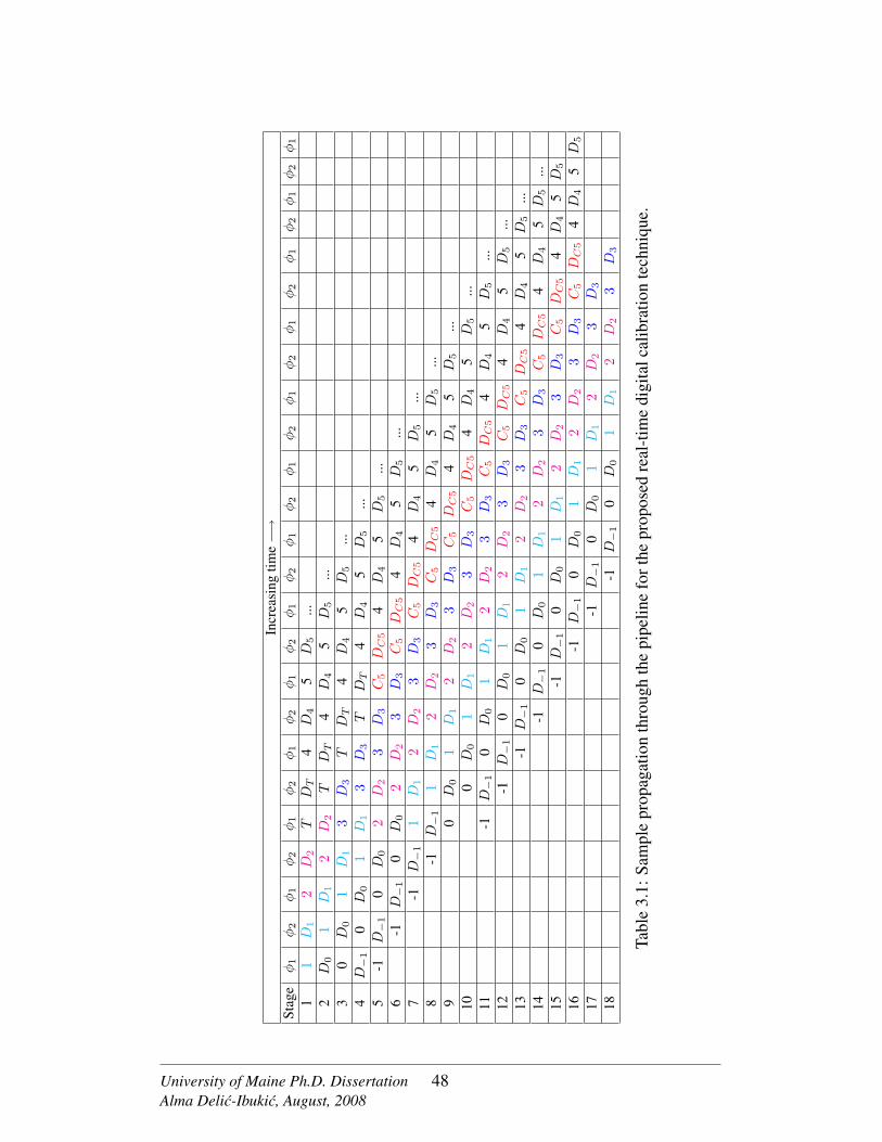
Incr
easi
ngtim
e−→
Stag
eφ
1φ
2φ
1φ
2φ
1φ
2φ
1φ
2φ
1φ
2φ
1φ
2φ
1φ
2φ
1φ
2φ
1φ
2φ
1φ
2φ
1φ
2φ
1φ
2φ
1
11
D1
2D
2T
DT
4D
45
D5
...2
D0
1D
12
D2
TD
T4
D4
5D
5...
30
D0
1D
13
D3
TD
T4
D4
5D
5...
4D−
10
D0
1D
13
D3
TD
T4
D4
5D
5...
5-1
D−
10
D0
2D
23
D3
C5
DC
54
D4
5D
5...
6-1
D−
10
D0
2D
23
D3
C5
DC
54
D4
5D
5...
7-1
D−
11
D1
2D
23
D3
C5
DC
54
D4
5D
5...
8-1
D−
11
D1
2D
23
D3
C5
DC
54
D4
5D
5...
90
D0
1D
12
D2
3D
3C
5D
C5
4D
45
D5
...10
0D
01
D1
2D
23
D3
C5
DC
54
D4
5D
5...
11-1
D−
10
D0
1D
12
D2
3D
3C
5D
C5
4D
45
D5
...12
-1D−
10
D0
1D
12
D2
3D
3C
5D
C5
4D
45
D5
...13
-1D−
10
D0
1D
12
D2
3D
3C
5D
C5
4D
45
D5
...14
-1D−
10
D0
1D
12
D2
3D
3C
5D
C5
4D
45
D5
...15
-1D−
10
D0
1D
12
D2
3D
3C
5D
C5
4D
45
D5
16-1
D−
10
D0
1D
12
D2
3D
3C
5D
C5
4D
45
D5
17-1
D−
10
D0
1D
12
D2
3D
3
18-1
D−
10
D0
1D
12
D2
3D
3
Tabl
e3.
1:Sa
mpl
epr
opag
atio
nth
roug
hth
epi
pelin
efo
rthe
prop
osed
real
-tim
edi
gita
lcal
ibra
tion
tech
niqu
e.
University of Maine Ph.D. DissertationAlma Delic-Ibukic, August, 2008
48

STA
GE
10
STA
GE
1ST
AG
E 5
STA
GE
4ST
AG
E 9
STA
GE
3ST
AG
E 2
STA
GE
7ST
AG
E 6
cal.
logi
cca
l. lo
gic
cal.
logi
cca
l. lo
gic
cal.
logi
cca
l. lo
gic
cal.
logi
cca
l. lo
gic
cal.
logi
cca
l. lo
gic
q 4q 6
q 8q 10
GG
1
STA
GE
8V
in
GG
//
G/
G
q 1q
q2
3q 5
q 7q 9
G
2G
G
/4
G
GGG
GG
G
10
2031
2 453
6
4
7
53
67
ωω
ωω
Figu
re3.
7:Pr
opos
edre
al-t
ime
digi
talc
alib
ratio
nar
chite
ctur
e.
University of Maine Ph.D. DissertationAlma Delic-Ibukic, August, 2008
49

for an 8-stage, 1-bit per stage pipeline converter. Stages 9 and 10 are active only during
the calibration process. In the figure, only stages 1 through 4 are calibrated, and stages
5 through 8 are assumed to be fabricated with sufficient accuracy. Each “calibration
logic” block has two weights associated with the given stage. One set of weights is used
only during the calibration process and reflect the reorganization of the pipeline during
calibration instant. The other set of weights goes with the normal converter operation.
In the case of the first four stages, these weights are programmable and their corrected
version ωi is obtained during calibration. Programmable weights are labeled ωi, where
i corresponds to stage numbers 1 through 4.
3.5 Verilog Implementation and Results
The proposed continuous calibration was implemented in Verilog Hardware De-
scription Language (HDL). A state machine that controls the calibration procedure is
discussed in Section 3.5.1. Required stage and digital encoder block modifications are
discussed in Sections 3.5.2 and 3.5.3. A 14-bit pipeline ADC implemented using 16
identical stages and 1-bit per stage topology is used for verification of the developed
calibration technique. Results are presented in Section 3.5.4. Also, the complexity of
the design is evaluated and presented in Section 3.5.5.
3.5.1 Finite State Machine (FSM) Description
Finite State Machines (FSMs) have been shown to be very efficient in modelling
sequential circuits [77]. The designed state machine controls the calibration process of
each stage, the predetermined data path shift that occurs during calibration, activation of
the extra two stages at the end of the pipeline, and writing of the corrected ωi value back
to the pipeline stage being calibrated. Two passes per stage are necessary to determine
the correction term ωi for that stage. A state machine was designed for a 14-bit pipeline
ADC implemented using 16 identical stages with gains less than two and 1-bit per stage
University of Maine Ph.D. DissertationAlma Delic-Ibukic, August, 2008
50

topology. Two extra stages are added at the end of the pipeline for a continuous time
calibration purposes. This makes a total of 18 identical pipeline stages. Only the first
seven stages are calibrated and have programmable weights associated with each stage.
The state machine is clocked using one of the non-overlapping clocks, φ1. A signal
coming from the FSM will stay ‘high’ for the entire clock period of φ1. Two non-
overlapping clocks are used to operate a pipeline ADC. During a ‘low’ time of φ1, the
second clock signal φ2 will be active and therefore, the necessary changes within the
even stages can be made.
As mentioned before, the FSM controls the sequence of the events essential for
the continuous calibration scheme to succeed. On the converter power up, and before
‘Calibration’ signal occurs, the ‘Reset’ signal must be asserted. Once the ‘Reset’ sig-
nal occurs, nineteen clock cycles are necessary to initialize the weights of all eighteen
pipeline stages. Each stage is initialized in turn with two weights. One set of weights
is associated with the normal operation of the converter, and a second set of shifted
weights is required for the (re)calibration process. At any instant (after the nineteen
clock cycles have passed), the ‘Calibration’ signal can occur. The master FSM con-
trols the calibration sequence. The calibration process is conducted starting with the last
stage in the pipeline being calibrated and moving toward the front of the pipeline. A
slave FSM counts clock cycles needed to start the calibration of a given stage and con-
trols the timing associated with the capture of the digital representation of the S1 and S2
terms shown in Figure 3.5. The state machine uses a clock counter to control the timing
of all calibration steps. To obtain a digital representation of S1 or S2 for a single stage,
nine clock cycles are required. The designed slave state machine uses 11 clock cycles.
This allows for the correction term to be calculated and written back to the calibrated
stage. Therefore, to obtain a correction term, ωi, for a single stage, 22 clock cycles are
necessary. The calculated weight, ωi, is the difference between the digital representa-
tions of S1 and S2. To calibrate 7 stages a total of 154 clock cycles are needed. The
University of Maine Ph.D. DissertationAlma Delic-Ibukic, August, 2008
51

ADCsub
+−
+ rGi i
ei
21q( )VREFi
qi
subDAC
controlled by thefinite state machine
i−1r
ri−3
S/H
0 or 1
(odd stage only)
Figure 3.8: Modifications required for a stage to be calibrated (dashed boxes).
sampling rate for the converter implemented is 51.2 MHz. At this speed, the converter
requires a total time of 3 µs to complete a calibration of 7 stages.
In addition to monitoring the calibration status of a stage, the clock counter is
responsible for setting and resetting different calibration lines for each stage. Calibration
lines have functions such as forcing the input to a sub-DAC to 0 or 1 when a stage is
being calibrated, changing the input data path, activating the extra two stages at the
end of the pipeline, monitoring the correct digital output collection sequence during
calibration period and writing the corrected term after calibration back to the calibrated
stage. Once all 7 stages have been calibrated the state machine is idle until the next
calibration signal is initiated.
3.5.2 Required Stage Modifications
Pipeline stages must be modified for the FSM to be able to make adjustments to
a stage while calibrating. All odd stages in the pipeline need to be capable of switching
a data path during the calibration process. Also, stages being calibrated must have
an option to select a ground for an input and to select forced sub-DAC inputs at the
calibration instant. The calibration instant for a given stage is controlled by the FSM.
Figure 3.8 shows the additional digital logic required by a stage being calibrated.
University of Maine Ph.D. DissertationAlma Delic-Ibukic, August, 2008
52

3.5.3 Error Correction Logic Modification
Most of the modifications regarding the digital calibration techniques are made
inside the digital encoder block. Digital calibration relies on measuring the error con-
tributions of the stage in digital domain and using these measured values to form the
ADC output code. The digital encoder block is where the ADC output code is formed,
therefore it plays a major role during the calibration process.
For the real-time digital calibration technique described in Section 3.4.2, the
digital encoder block must:
1. Form the ADC output code during normal operation of the converter.
2. Form the ADC output code during calibration process without interrupting the
converter’s operation.
3. During calibration process, obtain the correction terms to be used to form the
ADC output and write these terms back to a stage being calibrated for later use.
Figure 3.9 shows the digital encoder block modification for anN -stage converter
with 1-bit per stage architecture and two additional stages at the end of the pipeline
used during calibration. The digital encoder block consists of N + 2 adders (including
the extra two stages) pipelined together. The logic controlling the first seven adders is
different from the rest of the pipeline because the first seven stages can be calibrated.
During the normal converter operation each stage provides the digital encoder block with
the intermediate bit, qi, where i designates the stage number. Depending on the value
of qi, these weights will be added accordingly to form the ADC output code. The first
seven stages of a pipeline ADC have programmable weights initially set to ωi = Gi−1
and replaced as the correction term ωi is obtained during the calibration process. During
the calibration period, select lines from the FSM control the data path changes between
the stages to prevent interruption of the normal converter operation. For example, Stage
3 acts as a first stage in a pipeline when forming the coarse digital output. This select line
University of Maine Ph.D. DissertationAlma Delic-Ibukic, August, 2008
53

++
G1
+G
0
������������
��������
DIG
ITA
L O
UT
PUT
OF
TH
E C
ON
VE
RT
ER
dete
rmin
ed b
y th
e fi
nate
sta
te m
achi
ne.
−
++
+
fini
te s
tate
mac
hine
q 1q 2
GN
−2
G N
−1
+
GN
−1
q 3
++
GN
−3
G
/G
q
N−
55
N−
3
5
q
GG0 2
q N+
1N
q N+
2
TW
O E
XT
RA
ST
AG
ES
USE
D D
UR
ING
CA
LIB
RA
TIO
N P
RO
CE
SS
q
/
GG6
N−
4
N−
6
6
G
/G
q
N−
5
7N
−7
7
OB
TA
ININ
G C
OR
RE
CT
ION
TE
RM
S FO
R T
HE
ST
AG
ES
BE
ING
CA
LIB
RA
TE
D.
Stor
ed d
igita
l val
ue w
hen
sub−
DA
C in
put i
s se
t to
0.
Sub−
DA
C in
put
is s
et to
1.
for
a st
age
FLA
GFL
AG
FLA
G
FLA
G
FLA
GFL
AG
//
cont
rolle
d by
the
q
/
GG4
N−
2
N−
4
4
FLA
G1
2ω
ω3
/ω
ω
ωω
ω
FLA
GFL
AG
=0
Cor
rect
ed w
eigh
t
Figu
re3.
9:M
odifi
eder
ror
corr
ectio
nlo
gic
for
are
al-t
ime
digi
talc
alib
ratio
nsc
hem
eim
plem
enta
tion.
Exa
mpl
eofN
-sta
geco
nver
ter
with
1-bi
tper
stag
ear
chite
ctur
e.
University of Maine Ph.D. DissertationAlma Delic-Ibukic, August, 2008
54

is used only for one clock cycle at the start of the calibration procedure. The FSM lines
also control the use of the second set of weights which are attributed to each stage for
use during calibration process, and the FSM lines enable calibration of a stage itself. If
a particular stage is being calibrated, the coarse digital output for that stage is set to zero
(and later, to one) and the rest of the pipeline resumes the normal converter operation to
obtain the correction term ωi for the calibrated stage. The FSM select lines also control
the stages from which the ADC output will be taken. The green lines labelled FLAG in
Figure 3.9, are used during the calibration process to allow each stage to communicate
to the next stage if the second set of weights is to be used when adding the previous stage
output. All flags (except stages 1 and 2) are set to one at the start of calibration cycle.
Each stage then latches the value of FLAG from the previous stage on every clock edge.
The FLAG values propagate through the pipeline as an indicator that the corresponding
sample has been shifted in the pipeline, and the second set of weights should be used
when forming the ADC output code.
3.5.4 Results of the Developed Calibration Technique
The calibration scheme was implemented using Verilog HDL and simulated us-
ing the Verilog-XL simulator. The real-time calibration technique was derived for a
14-bit ADC with 1-bit per stage architecture implemented using 18 identical stages (in-
cluding two extra stages for calibration purposes). The last two stages in the pipeline
are active only during the calibration process. To verify that the real-time calibration
technique works, it was necessary to model a pipeline stage in Verilog HDL and also to
control gain, threshold and sub-DAC reference voltages of the stages being calibrated.
To model the behavior of the pipeline ADC, fully digital odd and even stages were cre-
ated using Verilog HDL. Gain, threshold and sub-DAC reference voltages were made
control variables at the input of each simulated pipeline stage. The nominal gain for all
18 stages was set to 1.81. The input range (VFS) for this converter was set to ±1.12
University of Maine Ph.D. DissertationAlma Delic-Ibukic, August, 2008
55

0 200 400 600 800 1000 1200
−20
−10
0
10
20
30
40
Sample Number
Res
idua
l Err
or (
LSB
)
SFDR = 97.1424 dB
SINAD = 78.4418 dB
ENOB = 12.7378 bits
SFDR = 70.6884 dB
SINAD = 65.4244 dB
ENOB = 10.5755 bits
+2 LSB
−2 LSB
calib
ratio
n st
arts
real−time calibration (Verilog HDL)
Figure 3.10: Residual error characteristics for a simulated ADC with applied real-timecalibration and errors introduced in all 18 stages of the converter.
V and the reference voltage for the converter was set to VREF = 1 V. A sampling fre-
quency of 51.2 MHz was used and the sinusoidal test signal was set to 150 kHz with the
amplitude at -1 dBFS (994 mV). Errors were introduced in all 18 stages (including two
extra stages used during calibration) of the converter and 1024 samples were collected.
Capacitor matching error between 0.1-0.5% was simulated. For threshold voltage varia-
tions, an error up to 10% of VFS was simulated. This is the maximum error allowed for
the chosen gain. Verilog-XL simulation results were collected and evaluated in MAT-
LAB. Figure 3.10 shows the residual error characteristics for a simulated 14-bit ADC
calibrated in a real-time. Before activating the calibration signal, the error contributions
from all 16 stages on the final resolution of an ADC is evident in Figure 3.10. The ADC
behaves as a 10-bit converter before calibration and as 12.7 bit converter after calibra-
tion. Once the calibration signal is activated, 154 clock cycles are needed for completion
of the calibration process.
University of Maine Ph.D. DissertationAlma Delic-Ibukic, August, 2008
56

3.5.5 Complexity of the Real-Time Calibration Logic
Verilog modules needed to implement the calibration technique were imported
in BuildGates Extreme and synthesized using a ‘generic build’ command in the Ca-
dence design environment. This produces unoptimized digital logic necessary to im-
plement the real-time calibration. The number of required transistor gates was approxi-
mated from the synthesized worse case model. Based on the synthesizer, approximately
100,000 logic gates are needed to implement the derived calibration. For a minimum
feature size of 65 nanometers the required area to implement the derived calibration
logic is approximately 0.07 mm2, based on the ITRS report from year 2007 [49]. This
is a fully digital logic design and therefore, the required area scales down easily with
new process technologies. Also, if this worse case model (100,000 logic gates) is to be
implemented in ASIC (Application Specified Integrated Circuit) design, the currently
available ASIC structures would dissipate on average 0.45 mW of power per MHz. This
is based on the IBM Cu-65HP ASIC - 65 nm process technology with power dissipation
of 4.5 nW/MHz/gate. If power is of a major concern, one way of reducing it would be by
activating calibration logic periodically and therefore making the calibration algorithm
non-continuous. For example, to calibrate first seven stages of a 16-stage pipeline con-
verter 154 clock cycles are required. If the sampling rate is 51.2 MHz converter requires
a total time of 3 µs to complete calibration of 7 stages. To reduce a power consumption
calibration logic can be activated every second, instead of having it run continuously.
University of Maine Ph.D. DissertationAlma Delic-Ibukic, August, 2008
57
CHAPTER 4
Hadamard Modulated ∆Σ A/D Converter Calibration Techniques
This chapter provides a general discussion of modulation based converter archi-
tectures. This is followed by examples of Hadamard modulated ∆Σ converters imple-
mented using 8 and 16 channels. Hadamard modulated ∆Σ converters are also known
as Π∆Σ ADCs [18, 19]. Following the two examples, the dominant error mechanisms
that can be present in Π∆Σ converters are discussed. Calibration techniques suitable
for these converter architectures are presented and their benefits and/or shortcoming are
analyzed. A new real-time digital calibration technique targeted for Π∆Σ architecture
converters is also introduced.
4.1 Overview of Modulation Based A/D Converter Architectures
Modulation based converter architectures use a collection of orthogonal periodic
modulation signals to decompose an input signal into M orthogonal channels. Each
channel is quantized, and the channels are then digitally recombined to form the wide-
bandwidth digital output. Valid modulation sequence sets are conveniently described
using unitary matrices [19, 20]. A unitary matrix is defined as an M × M complex
matrix U with a property that UU ∗ = I , where I is an identity matrix and ∗ denotes a
conjugate transpose [78]. If U contains only real elements and UUT = I , then U is
said to be orthogonal or orthonormal.
The rows of an M × M unitary matrix U correspond to a valid collection of
modulation sequences for parallel architecture. Each column of the matrix indicates a
time instance n. Let the sequence ur[n] = ur,n mod M indicate row elements of a unitary
matrix U extended in time (i.e. each row of U is repeated over and over again). Fig-
ure 4.1 shows a generic architecture for modulation based ∆Σ converters implemented
usingM channels. For analysis, the Lth order ∆Σ modulator may be replaced by its sig-
University of Maine Ph.D. DissertationAlma Delic-Ibukic, August, 2008
58

1u [n]
2u [n]
u [n]3
M−1u [n]
u [n]M
G(z)
3*
G(z)
1u [n−d]*
u [n−d]
G(z)
2*
G(z)
u [n−d]
y[n]u [n−d]*
M−1
G(z)
u [n−d]M*
∆Σ
∆Σ
∆Σ
∆Σ
∆Σ
G(z)~
x[n]
Figure 4.1: Generic architecture for modulation based ∆Σ converters.
nal transfer function STF (z) = z−m, as discussed in Section 2.4.3. The signal transfer
function introduces a fixed delay of m samples to each channel of the Π∆Σ ADC. Also,
to further simplify the analysis, the ∆Σ modulator and lowpass filter G(z) are grouped
into one system G(z). The delay introduced by G(z) contains delays introduced by both
the ∆Σ modulator and the lowpass filter G(z).
After the input signal x[n] is modulated by ur[n], the modulated input is passed
on to the system G(z). The output of G(z) is demodulated by a delayed sequence
u∗r[n− d], with ∗ indicating a complex conjugate and d indicating a delay through G(z),
which must be an integer value. The output of the overall system y[n] is then given by
y[n] =M∑r=1
∞∑k=0
(g[k]x[n− k]ur[n− k])u∗r[n− d]
=∞∑k=0
g[k]x[n− k]M∑r=1
ur[n− k]u∗r[n− d] (4.1)
University of Maine Ph.D. DissertationAlma Delic-Ibukic, August, 2008
59
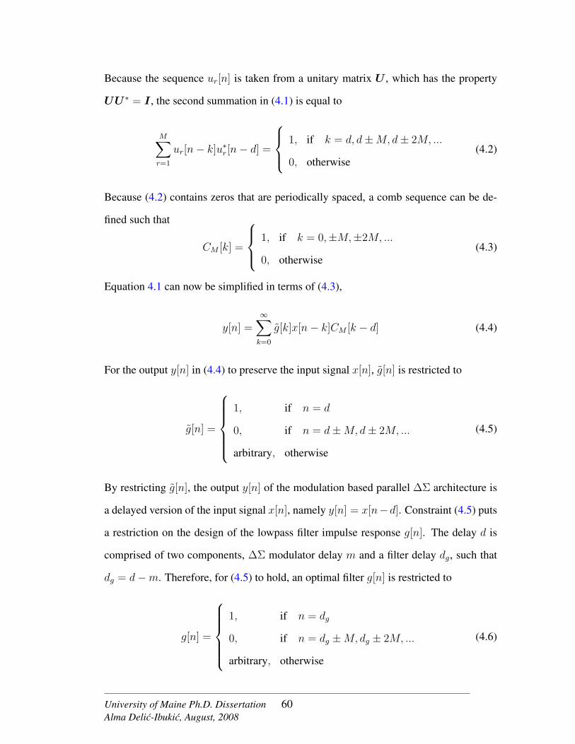
Because the sequence ur[n] is taken from a unitary matrix U , which has the property
UU ∗ = I , the second summation in (4.1) is equal to
M∑r=1
ur[n− k]u∗r[n− d] =
1, if k = d, d±M,d± 2M, ...
0, otherwise(4.2)
Because (4.2) contains zeros that are periodically spaced, a comb sequence can be de-
fined such that
CM [k] =
1, if k = 0,±M,±2M, ...
0, otherwise(4.3)
Equation 4.1 can now be simplified in terms of (4.3),
y[n] =∞∑k=0
g[k]x[n− k]CM [k − d] (4.4)
For the output y[n] in (4.4) to preserve the input signal x[n], g[n] is restricted to
g[n] =
1, if n = d
0, if n = d±M,d± 2M, ...
arbitrary, otherwise
(4.5)
By restricting g[n], the output y[n] of the modulation based parallel ∆Σ architecture is
a delayed version of the input signal x[n], namely y[n] = x[n−d]. Constraint (4.5) puts
a restriction on the design of the lowpass filter impulse response g[n]. The delay d is
comprised of two components, ∆Σ modulator delay m and a filter delay dg, such that
dg = d−m. Therefore, for (4.5) to hold, an optimal filter g[n] is restricted to
g[n] =
1, if n = dg
0, if n = dg ±M,dg ± 2M, ...
arbitrary, otherwise
(4.6)
University of Maine Ph.D. DissertationAlma Delic-Ibukic, August, 2008
60

For a discrete time ∆Σ modulator, the ADC delay m is an integer. To obtain an integer
system delay d, the lowpass filter delay dg must also be designed as a fixed integer value.
This further restricts the design of g[n] to an odd-length linear phase filter.
As seen from the above discussion, modulation based parallel ∆Σ converter ar-
chitectures will preserve the input signal as long as the criteria for the filter g[n] and mod-
ulation signal are met: filter behavior is restricted by (4.6); and the modulation signal
is derived from a unitary matrix. Common unitary matrices used to modulate the input
signal of a parallel architecture ∆Σ converters are: DFT (Discrete Fourier Transform)
matrix, identity matrix and Hadamard matrix [19, 20, 73]. Modulation based architec-
tures that are implemented using the identity matrix are also known as time-interleaved
converter architectures. Time-interleaved converter architectures are discussed in Sec-
tion 2.5.1 [16,17,20,67,68]. The DFT modulation based parallel architecture converters
are discussed in Section 2.5.2. The disadvantage of DFT modulation is the requirement
of complex modulators which are difficult to realize in hardware [14,20,73]. Hadamard
modulated parallel ∆Σ converter architectures use a Hadamard matrix, which is com-
posed of ±1’s as a modulation signal. Also, Hadamard modulated architectures can be
extended to exploit oversampling. This allows not just for the increase in the overall
bandwidth, but also increase in the overall converter resolution [19].
4.2 Oversampling Π∆Σ A/D Converter Architecture
Hadamard modulated ∆Σ converters are also known as Π∆Σ converters [18,19].
This section gives an overview of Π∆Σ A/D converter architectures and their imple-
mentation when oversampling is used. Following the overview of the Π∆Σ architecture
converter, an example of an 8-channel and a 16-channel oversampling Π∆Σ converter
will be presented.
University of Maine Ph.D. DissertationAlma Delic-Ibukic, August, 2008
61

D
D
D
D
DG(z)
G(z)~
G(z)
G(z)
G(z)
G(z)
Ms [n]
M−1s [n]
1
2
3
x[n]
y[n]
s [n]
s [n]
s [n]
∆ Σ
∆ Σ
∆ Σ
∆ Σ
∆ Σ
1
2
3
M−1
M
h [n]
h [n]
h [n]
h [n]
h [n]
Figure 4.2: Π∆Σ A/D converter architecture with oversampling.
4.2.1 Overview of Π∆Σ A/D Converters
As shown in Section 4.1, modulation based ∆Σ converters can be implemented
using any external signal, as long as it is derived from a unitary matrix. A Hadamard
matrix H is an M ×M matrix which is proportional to a unitary matrix. H consists
only of ±1’s and therefore is easy to realize in hardware. For the Hadamard matrix
to exist, M must be a positive power of two, meaning M = 2l+1. This in turn puts a
constraint on number of channels in the parallel configuration. The lth Hadamard matrix
is defined recursively by
Hl =
Hl−1 Hl−1
Hl−1 −Hl−1
, H0 =
1 1
1 −1
(4.7)
and it has a property HHT = MI , where I is identity matrix. Each row of the
Hadamard matrix H corresponds to the modulation sequence for a single channel, and
each column corresponds to a sampling instance n. Figure 4.2 shows an M-channel
University of Maine Ph.D. DissertationAlma Delic-Ibukic, August, 2008
62

Hadamard modulated parallel ∆Σ ADC that employs oversampling D. Each channel
consist of a conventional Lth order ∆Σ modulator and decimation filter G(z). To sim-
plify the analysis of the signal component, the D-fold downsampler can be ignored, and
the Lth order ∆Σ modulator is replaced by its signal transfer function STF (z) = z−m.
This reflects the fixed delay of m samples associated with the modulator. Also, the ∆Σ
modulator and lowpass filterG(z) are grouped into one system with the transfer function
G(z).
By ignoring downsampling, the Hadamard modulation sequences sr[n] and hr[n]
become sr[n] and sr[n− d], respectively; where d is the delay introduced by the system
G(z) and sequence sr[n] = sr,n mod M indicates the rth row elements ofH that is extend
in time. Therefore, from Figure 4.2 with downsampling ignored, the output of the overall
system y[n] is given by
y[n] =M∑r=1
∞∑k=0
(g[k]x[n− k]sr[n− k])sr[n− d]
=∞∑k=0
g[k]x[n− k]M∑r=1
sr[n− k]sr[n− d] (4.8)
Because the sequence sr[n] is taken from a Hadamard matrix H that has a property
HHT = MI , the second summation in (4.8) is equal to
M∑r=1
sr[n− k]sr[n− d] =
M, if k = d, d±M,d± 2M, ...
0, otherwise(4.9)
Equation 4.9 has periodically spaced zeros and as such can be written in terms of the
comb sequence that was defined in (4.3). Rewriting (4.8) in terms of CM [k] gives
y[n] = M∞∑k=0
g[k]x[n− k]CM [k − d] (4.10)
University of Maine Ph.D. DissertationAlma Delic-Ibukic, August, 2008
63

For the output y[n] to preserve the input signal x[n], g[n] is restricted to
g[n] =
1/M, if n = d
0, if n = d±M,d± 2M, ...
arbitrary, otherwise
(4.11)
By restricting g[n] the overall output of the Hadamard modulated parallel ∆Σ A/D con-
verter y[n] is a delayed version of the input signal, namely y[n] = x[n − d]. The
constraint (4.11) puts a restriction on the design of the lowpass filter g[n]. The overall
delay through G(z) is given by d = m + dg, where m is the delay through an Lth or-
der modulator and dg is a delay through a lowpass filter G(z). For (4.11) to hold, the
impulse response g[n] is restricted to
g[n] =
1/M, if n = dg
0, if n = dg ±M,dg ± 2M, ...
arbitrary, otherwise
(4.12)
where dg = d − m. As mentioned in Section 4.1, d and m are integer values which
further restricts the design of g[n] to an odd-length linear phase filter.
The design of an optimal filter g[n] involves the selection of the undetermined
coefficients in (4.12) and is discussed in [18]. Alternative filter architectures that are
not restricted to (4.12) but may be more simple to implement can be used. In this case,
the overall output y[n] of Π∆Σ architecture is not just a delayed version of the input
signal x[n]. The distortion in the overall output y[n] that may be caused by the use of
non-optimal filterG(z) can be recovered (if necessary) by implementing an equalization
filter [18,19]. The equalization filter would come after the output of the Π∆Σ ADC and
therefore only one such filter would be required. Equalization filter designs for Nyquist-
rate and oversampling Π∆Σ ADCs are discussed in [18, 19].
Oversampled ∆Σ converter architectures are desirable because they improve the
University of Maine Ph.D. DissertationAlma Delic-Ibukic, August, 2008
64

overall resolution of the converter as discussed in Section 2.4.3. Applying oversampling
to Π∆Σ architecture converters results in an increase of the overall converter bandwidth
and resolution [19]. When oversampling is used, the Hadamard modulation sequences
sr[n] and hr[n] from Figure 4.2 must be modified. If hr[n] = hr,n mod M indicates the rth
row elements ofH that are extended in time, then sr[n] must be modified and advanced
to take into account oversampling and delay through ∆Σ modulator and lowpass filter
G(z) [19]. The sequence sr[n] in terms of hr[n] is given by
sr[n] = hr
(⌊n+ d+ D−1
2
D
⌋), (4.13)
where D is the oversampling ratio, d is the delay through the system G(z), and the inner
brackets round towards minus infinity. The delay d is given by
d =J − 1
2+m (4.14)
where J is the length of a lowpass filter G(z) and m is the delay through the Lth order
∆Σ modulator. To obtain an integer result for a total system advance, J andD are either
both even or both odd integers.
Alternative filter architectures that are not restricted to (4.12), and are simpler
to implement can be used in the design of G(z). The lowpass filter G(z) must be de-
signed to minimize the quantization noise contribution in a desired signal band. In the
case of conventional ∆Σ converter architectures, the in-band quantization noise power
is reduced by using comb filters that have zeros placed at 1/D and its multiples, where
D is the oversampling ratio as was discussed in Section 2.4.3. For the parallel ∆Σ ar-
chitecture converters, the overall quantization noise power comes from the contribution
of M parallel channels [19]. Hardware efficient filters for Π∆Σ converter architectures
that minimize the overall in-band quantization noise power are derived in [19]. The
University of Maine Ph.D. DissertationAlma Delic-Ibukic, August, 2008
65

recommended filter is combL+1 filter having the transfer function
G(z) =
(1
DM
)L+1(1− z−DM
1− z−1
)L+1
(4.15)
where L is the ∆Σ modulator order, M is the number of channels used in parallel
configuration and D is the oversampling ratio. The length of a comb filter described
in (4.15) is given by J = (DM)(L+ 1)−L. In case an integer result for a total system
advance is not satisfied, an alternative comb filter architecture can be used [18, 19],
where one comb filter stage is changed,
G(z) =
(1
DM
)L(1
DM + 1
)(1− z−DM
1− z−1
)L(1− z−(DM+1)
1− z−1
). (4.16)
The new filter length is given by J = (DM)(L+ 1)− L+ 1.
For the combL+1 filter described by (4.15), zeros are located at 1/DM and its
multiples. The bandwidth of the decimation filter G(z) is smaller by a factor of M ,
relative to the conventional ∆Σ converter. By using a filter described by (4.15), an
M -channel Π∆Σ converter with oversampling ratio of D will achieve performance
approaching a conventional ∆Σ converter with oversampling ratio of M × D. How-
ever, there is a 12
log2(M)-bit penalty in accuracy that is associated with parallel struc-
tures [19].
4.2.2 Simulation of Π∆Σ A/D Converters
To illustrate the benefits of parallel architecture converters, a Π∆Σ ADC was
simulated in MATLAB. Both 8-channel and 16-channel oversampling Π∆Σ converter
architecture were modelled, with each channel containing 2nd order ∆Σ modulators with
a 1-bit quantizer (ADC) and decimation filter described by (4.15). Also, an equalization
filter described in [19] was implemented to recover any distortion in the overall converter
output that is caused by the use of non-optimal filter. The oversampling ratio D = 4 is
University of Maine Ph.D. DissertationAlma Delic-Ibukic, August, 2008
66

z−1k1
1−z−1z−1
1−z−1
k2x[n] y[n]
e[n]
+ + −−
Figure 4.3: Linear model for a second order ∆Σ modulator used in simulations.
used in both examples.
Figure 4.3 shows the linear model of a 2nd order ∆Σ modulator with a 1-bit
quantizer that is used in simulation. The ∆Σ modulator contains two delaying integra-
tors and is based on the design first introduced in [79]. By setting coefficients k1 and
k2 to 0.5 and 2, respectively and by using a z-transform, the output y[n] in Figure 4.3 is
given by
Y (z) = X(z)z−2 + E(z)(1− z−1)2
= X(z)STF (z) + E(z)NTF (z) (4.17)
The STF (z) is the signal transfer function and NTF (z) is the noise transfer func-
tion which are described in Section 2.4.3. The 1-bit quantizer is modelled as an addi-
tive white noise source e[n] with samples uniformly distributed within ±Q1/2 interval,
where Q1 is the quantization interval described in Section 2.4.1. For a 1-bit quantizer,
the quantization interval is given by Q1 = 2VREF/2 = VREF , where ±VREF is the
allowable input signal range of the quantizer (1-bit ADC).
A general setup for an M -channel oversampling Π∆Σ converter architecture
is shown in Figure 4.2. Equation (4.7) was used to generate Hadamard (de)modulation
sequences for 8-channel and 16-channel Π∆Σ ADCs and (4.13) is used to create a front-
end Hadamard modulation sequence that takes into account oversampling. The 8 × 8
University of Maine Ph.D. DissertationAlma Delic-Ibukic, August, 2008
67

Hadamard matrix for an eight channel Π∆Σ converter is
H2 =
1 1 1 1 1 1 1 1
1 −1 1 −1 1 −1 1 −1
1 1 −1 −1 1 1 −1 −1
1 −1 −1 1 1 −1 −1 1
1 1 1 1 −1 −1 −1 −1
1 −1 1 −1 −1 1 −1 1
1 1 −1 −1 −1 −1 1 1
1 −1 −1 1 −1 1 1 −1
.
The rth row of the Hadamard matrix corresponds to modulation sequence for the rth
channel, and each column represents the time instance. Although the Hadamard modu-
lation sequences are not simply a frequency decomposition, the modulation sequences
do have distinct and recognizable spectral characteristics. For the eight-channel exam-
ple, rows three and four have the same fundamental frequency FS/4, where FS is the
Nyquist-rate clock, but differ in phase. The same is true for rows five, six, seven and
eight which share the same frequency FS/8. Figure 4.4 illustrates the frequency content
of the rows of an 8×8 Hadamard matrix. Numbers 1 though 8 correspond to Hadamard
matrix rows. Each channel (or multiple channels) of a Π∆Σ architecture modulates dif-
ferent frequency band of an input signal with bandwidth of FS/2. The noticeable bumps
in the noise floor mimic the noise shaping function of ∆Σ modulators.
Figures 4.5 and 4.6 show simulation results for an 8-channel and a 16-channel
Π∆Σ converter implemented using an oversampling ratio of D = 4 and a single tone
input signal. The signal amplitude was at -1 dB of full scale (dBFS). The noticeable
bumps in the noise floor are due to the noise shaping transfer function NTF (z) of a
2nd order ∆Σ modulator. In both cases, the input bandwidth FS/2 is preserved by the
oversampling Π∆Σ converter architecture. Also, the Hadamard decomposition of the
University of Maine Ph.D. DissertationAlma Delic-Ibukic, August, 2008
68

FS0 SFS FSF
8 4 8 2
3 F
5,6,7,8 25,6,7,81 3,4F
requ
ency
spe
ctru
m
Figure 4.4: Frequency spectrum of 8 by 8 Hadamard matrix. Numbers 1 through 8indicate Hadamard matrix rows and FS is the Nyquist-rate clock.
0 0.05 0.1 0.15 0.2 0.25 0.3 0.35 0.4 0.45 0.5−140
−120
−100
−80
−60
−40
−20
0
Normalized Frequency
Mag
nitu
de, d
BFS
ENOBΠ∆Σ= 8.45 bits
ENOB∆Σ= 10.19 bits
Figure 4.5: Simulation results for an 8-channel Π∆Σ A/D converter with oversamplingratio D = 4. Normalized frequency is given by F/FS .
University of Maine Ph.D. DissertationAlma Delic-Ibukic, August, 2008
69

0 0.05 0.1 0.15 0.2 0.25 0.3 0.35 0.4 0.45 0.5−140
−120
−100
−80
−60
−40
−20
0
Normalized Frequency
Mag
nitu
de, d
BFS
ENOBΠ∆Σ=10.48ENOBΠ∆Σ=10.48 bits
ENOB∆Σ=12.65 bits
Figure 4.6: Simulation results for a 16-channel Π∆Σ A/D converter with oversamplingratio D = 4. Normalized frequency is given by F/FS .
input bandwidth into M distinct frequency regions, where M corresponds to number of
channels, is evident. The M frequency regions are centered around zero (i.e. DC) and
multiples of 1/M .
In Section 4.2.1 it was noted that an M -channel Π∆Σ converter with oversam-
pling ratio of D will achieve performance approaching a conventional ∆Σ converter
with oversampling ratio of M × D. There is a 12
log2(M)-bit penalty associated with
a parallel architectures [19]. Figures 4.5 and 4.6 show the effective number of bits
(ENOB) for Π∆Σ and conventional ∆Σ converter architectures. ENOBΠ∆Σ is the ef-
fective number of bits for Π∆Σ converter and ENOB∆Σ is the effective number of bits
for a conventional ∆Σ converter with oversampling ratio M ×D. The performance dif-
ference between the two architectures is close to 1.5-bits and 2-bits, for 8-channel and
16-channel Π∆Σ ADC, respectively. The 12
log2(M)-bit difference in accuracy is in the
agreement with the theory derived in [19].
University of Maine Ph.D. DissertationAlma Delic-Ibukic, August, 2008
70

4.3 Dominant Errors in Π∆Σ ADCs
The Π∆Σ architecture described in Section 4.2 shows one way of trading circuit
complexity for increased resolution and/or bandwidth. However, the wide-bandwidth
and high-resolution results are achieved only if all M -channels in the parallel archi-
tecture are identical and Hadamard modulation sequences are in-sync. Channel mis-
matches are usually caused by variations in the manufacturing process. To preserve the
wide bandwidth and/or resolution that parallel converter architectures offer, errors such
as channel gain and offset mismatches need to be addressed. Following the discussion
of dominant errors in parallel architecture converters, an overview of current calibration
techniques suitable for Π∆Σ converter architectures is given.
4.3.1 Channel Gain and Offset Mismatch Errors
Besides the nonidealities that come with conventional ∆Σ modulators, Π∆Σ ar-
chitecture converters are sensitive to channel gain mismatches, offset mismatches and
Hadamard modulation level errors [18, 19, 64, 70, 71]. To simplify the analysis of chan-
nel mismatch errors in Π∆Σ converters, a Hadamard modulated converter without over-
sampling is analyzed. Figure 4.7 shows an idealM -channel Π∆Σ converter architecture
without oversampling. The sequence hr[n] = hr,n mod M indicates row elements of the
M×M Hadamard matrix. Each channel, as before, consists of a conventional Lth order
∆Σ modulator that is assumed to introduce a constant delay ofm samples, and decimat-
ing lowpass filter G(z). The lowpass filter G(z) and ∆Σ modulators are grouped into
one system, G(z). The system G(z) introduces a delay d that consists of both, delay
through the filter and ∆Σ modulator.
Dominant errors in Π∆Σ architecture converters are channel gain and offset
mismatch errors [18, 19, 64]. These errors introduce undesirable frequency tones in the
converter output, affecting its overall linearity and degrading the spurious-free-dynamic-
range (SFDR) and signal-to-noise-ratio (SNR). Figure 4.8 shows a model used to ana-
University of Maine Ph.D. DissertationAlma Delic-Ibukic, August, 2008
71

G(z)
1h [n−d]
2h [n−d]
3h [n−d]
y[n]M−1h [n−d]
Mh [n−d]
G(z)~
G(z)
G(z)
G(z)
M
M−1
1
x[n]∆ Σ
∆ Σ
∆ Σ
∆ Σ
∆ Σ
2
3
h [n]
h [n]
h [n]
h [n]
h [n]
G(z)
Figure 4.7: Π∆Σ architecture converter without oversampling.
y [n]r rw [n]G(z)~
rh [n−d]
1+ ε r
ra
offset, rh [n]r
x[n]
b
gain,
Figure 4.8: Model for gain and offset error in rth channel of Π∆Σ converters.
University of Maine Ph.D. DissertationAlma Delic-Ibukic, August, 2008
72

lyze gain and offset errors in the rth channel of a Π∆Σ converter shown in Figure 4.7.
The general expression for the output of the rth-channel, yr[n], including channel gain
and offset errors is given by
yr[n] =
(∞∑k=0
g[k](1 + εr)x[n− k]hr[n− k] + br
)hr[n− d]
=
(∞∑k=0
g[k]x[n− k]hr[n− k]
)hr[n− d]
+
(∞∑k=0
g[k]εrx[n− k]hr[n− k]
)hr[n− d] + brhr[n− d] (4.18)
and the overall output y[n] is given by
y[n] =M∑r=1
yr[n]
=∞∑k=0
g[k]x[n− k]M∑r=1
hr[n− k]hr[n− d]
+∞∑k=0
g[k]x[n− k]M∑r=1
εrhr[n− k]hr[n− d] +M∑r=1
brhr[n− d]
= x[n− d] +∞∑k=0
g[k]x[n− k]M∑r=1
εrhr[n− k]hr[n− d]
+M∑r=1
brhr[n− d] (4.19)
From (4.18) and (4.19) it can be seen that offset errors br are signal independent.
At the output of each channel, the offset errors are modulated by a delayed version
of hr[n], a single row of the M ×M Hadamard matrix. As shown in Section 4.2.2, an
M×M Hadamard matrix introduces frequency tones throughout the frequency spectrum
at multiples of 1/M of the Nyquist-rate clock FS . Therefore, with the offset errors
present, the output spectrum of y[n] will contain frequency tones at FS/M and multiples
of FS/M .
University of Maine Ph.D. DissertationAlma Delic-Ibukic, August, 2008
73
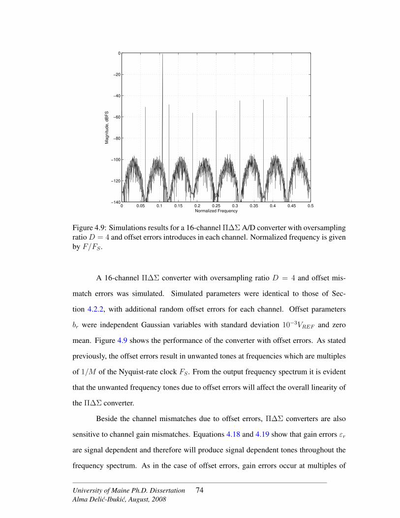
0 0.05 0.1 0.15 0.2 0.25 0.3 0.35 0.4 0.45 0.5−140
−120
−100
−80
−60
−40
−20
0
Normalized Frequency
Mag
nitu
de, d
BFS
Figure 4.9: Simulations results for a 16-channel Π∆Σ A/D converter with oversamplingratioD = 4 and offset errors introduces in each channel. Normalized frequency is givenby F/FS .
A 16-channel Π∆Σ converter with oversampling ratio D = 4 and offset mis-
match errors was simulated. Simulated parameters were identical to those of Sec-
tion 4.2.2, with additional random offset errors for each channel. Offset parameters
br were independent Gaussian variables with standard deviation 10−3VREF and zero
mean. Figure 4.9 shows the performance of the converter with offset errors. As stated
previously, the offset errors result in unwanted tones at frequencies which are multiples
of 1/M of the Nyquist-rate clock FS . From the output frequency spectrum it is evident
that the unwanted frequency tones due to offset errors will affect the overall linearity of
the Π∆Σ converter.
Beside the channel mismatches due to offset errors, Π∆Σ converters are also
sensitive to channel gain mismatches. Equations 4.18 and 4.19 show that gain errors εr
are signal dependent and therefore will produce signal dependent tones throughout the
frequency spectrum. As in the case of offset errors, gain errors occur at multiples of
University of Maine Ph.D. DissertationAlma Delic-Ibukic, August, 2008
74

0 0.2 0.4 0.6 0.8 1 1.2 1.4 1.6 1.8 2−140
−120
−100
−80
−60
−40
−20
0
Frequency (MHz)
Mag
nitu
de, d
BFS
FS/16,1
FS/16,−1
FS/8+F
INFS/8−F
IN
3FS/16,13F
S/16,−1
FS/4+F
IN
FS/4−F
IN
5FS/16,1
5FS/16,−1
3FS/8+F
IN
3FS/8−F
IN
7FS/16,1
7FS/16,−1
FS/2+F
IN
FS/2−F
IN
Figure 4.10: Simulations results for a 16-channel Π∆Σ A/D converter with oversam-pling ratio D = 4 and gain errors introduces in each channel. Labelled are gain errorspectrum peak locations fε.
1/M of the Nyquist-rate clock FS before being modulated by the input frequency FIN .
However, unlike offset errors, gain errors are signal dependent and their spectrum peaks
occur at
fε = iFSM± FIN , i = 1, 2, 3...M/2, (4.20)
where M is the number of channels in parallel configuration. A 16-channel Π∆Σ con-
verter with oversampling ratio D = 4 and gain mismatch errors was simulated in MAT-
LAB. The converter was simulated using same setup as in Section 4.2.2. Gain error
mismatches of ±1% were simulated and introduced to all channels. Figure 4.10 shows
the performance of a Π∆Σ converter with gain errors. The location of the spurious
peaks fε due to gain error are also labelled. As stated previously, the location of un-
wanted frequency tones are determined only by the input signal frequency FIN and the
frequency tones due to the M ×M Hadamard matrix (i.e. tones at multiples of 1/M of
the Nyquist-rate clock FS).
University of Maine Ph.D. DissertationAlma Delic-Ibukic, August, 2008
75

As was the case with offset errors, gain error mismatches degrade the overall
performance of parallel architecture converters. To preserve the linearity and band-
width that parallel architecture converters offer, some form of calibration needs to be
employed. Calibration techniques suitable for Π∆Σ ADCs are discussed next.
4.3.2 Calibration Techniques for Modulation-Based ADCs
Different foreground and background calibration techniques for modulation based
parallel converter architectures have been proposed [22,29–31,54,80]. Foreground cali-
bration techniques are repeated each time converter is powered up [30] and re-calibration
of the converter is possible. However, this requires a converter to be off-line while
(re)calibration is in progress. This type of calibration interrupts the normal operation
of the converter and it does not take into account changes in the environment that can
affect the performance of the converter. Background calibration techniques are the ideal
type of calibration [22, 29, 31, 54, 80]. While being calibrated, the converter is in its
normal mode of operation. Environmental and internal changes are taken into account
and corrected.
A foreground calibration technique for modulation based parallel ∆Σ converters
was reported in [30]. The technique corrects for channel gain and offset mismatch errors.
At converter startup, each channel of the parallel architecture will quantize a set of
known calibration voltages. These values are used to determine a set of calibration
coefficients for each channel. These are used to compensate for the mismatch in each
path using digital ∆Σ modulators which are area efficient and insensitive to process
variations.
Background calibration techniques for time-interleaved converter architectures
were reported in [22, 29, 31, 54, 80]. In [22] an analog calibration technique was dis-
cussed. The technique requires M + 1 time-interleaved converters and one reference
ADC to increase the overall system sample rate by M , where M is the number of chan-
University of Maine Ph.D. DissertationAlma Delic-Ibukic, August, 2008
76
nels in parallel configuration. At any time, M channels are running in time-interleaving
manner and one is taken off-line so the selected ADC can be calibrated. While off-line,
the selected ADC is calibrated to match the gain and offset errors of the reference ADC.
Once calibrated, the converter is placed back in the parallel configuration path and the
new (uncalibrated) channel is taken off-line for calibration. This calibration technique,
while effective for Nyquist-rate converters (i.e. pipeline ADCs), cannot be configured
for ∆Σ ADCs. The output of ∆Σ modulators depends on the input history. By period-
ically taking a single ∆Σ modulator off-line and reintroducing it back in a signal path
after some time, periodic deviations in a path history are created. Any deviations in the
output from the ideal one for a given channel will degrade the overall performance of
parallel architecture converters.
A digital background calibration technique for time-interleaved converter archi-
tectures was reported in [29]. To calibrate a channel gain mismatch, a calibration signal
that is uncorrelated with the input is added to the input. Both signals are then processed
by the ADC. The digital form of the calibration signal is than subtracted from the ADC
output. If the the gain error is present in the channel, the calibration signals will not can-
cel each other out through subtraction. By adding a variable gain in the ADC path and
updating it through an adaptive algorithm, the channel output can be driven to contain
only the input signal and nothing else. Because the subtractive dithering (i.e addition
of the noise to the signal) is employed, this calibration techniques is suited for Nyquist-
rate converters. Implementing subtractive dither in ∆Σ converter architectures is not
practical [63].
Digital background calibration techniques for time-interleaved ADC architec-
tures that were reported in [31, 80] are also applicable for calibration of Π∆Σ ADCs.
In [31], an additional channel is used as a reference element. The channel being cal-
ibrated is placed in parallel with the reference channel and calibration is preformed in
a digital domain through the use of a complex digital signal processing. Calibration of
University of Maine Ph.D. DissertationAlma Delic-Ibukic, August, 2008
77

the overall system depends on the number of parallel channels and the time required to
calibrate a single channel. The calibration technique discussed in [80] uses an adaptive
algorithm to corrected for channel mismatches. The gain and offset mismatches are cor-
rected relative to the first A/D converter in a parallel configuration. To converge, the
calibration algorithm assumes the same input statistics (i.e. mean, variance etc.) for all
channels.
The calibration techniques discussed above either cannot be applied to parallel
converter architectures that are built using ∆Σ modulators [22,29] or make assumptions
about the properties of the input signal [80]. The following section introduces a new
digital calibration technique that is targeted towards Π∆Σ converter architectures and is
independent of input signal statistics.
4.4 Real-Time Digital Calibration Algorithm Development
A novel real-time digital calibration approach that removes gain mismatch errors
between channels of Π∆Σ ADCs is described below. Calibration is accomplished by
adding an additional channel that is linearly dependant on the Π∆Σ channels used.
This redundancy in the system allows for gain errors within channels to be successfully
corrected.
The model used to analyze gain and offset errors in the rth channel of a Π∆Σ
converter was introduced in Section 4.3 and is shown in Figure 4.8. The general ex-
pression for the output of rth-channel before demodulation, including channel gain and
offset errors, is given by
wr[n] =∞∑k=0
g[k](1 + εr)x[n− k]hr[n− k] + br
=∞∑k=0
g[k]arx[n− k]hr[n− k] + br (4.21)
University of Maine Ph.D. DissertationAlma Delic-Ibukic, August, 2008
78
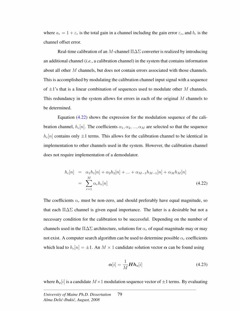
where ar = 1 + εr is the total gain in a channel including the gain error εr, and br is the
channel offset error.
Real-time calibration of anM -channel Π∆Σ converter is realized by introducing
an additional channel (i.e., a calibration channel) in the system that contains information
about all other M channels, but does not contain errors associated with those channels.
This is accomplished by modulating the calibration channel input signal with a sequence
of ±1’s that is a linear combination of sequences used to modulate other M channels.
This redundancy in the system allows for errors in each of the original M channels to
be determined.
Equation (4.22) shows the expression for the modulation sequence of the cali-
bration channel, hc[n]. The coefficients α1, α2, ..., αM are selected so that the sequence
hc[n] contains only ±1 terms. This allows for the calibration channel to be identical in
implementation to other channels used in the system. However, the calibration channel
does not require implementation of a demodulator.
hc[n] = α1h1[n] + α2h2[n] + ...+ αM−1hM−1[n] + αMhM [n]
=M∑r=1
αrhr[n] (4.22)
The coefficients αr must be non-zero, and should preferably have equal magnitude, so
that each Π∆Σ channel is given equal importance. The latter is a desirable but not a
necessary condition for the calibration to be successful. Depending on the number of
channels used in the Π∆Σ architecture, solutions for αr of equal magnitude may or may
not exist. A computer search algorithm can be used to determine possible αr coefficients
which lead to hc[n] = ±1. An M × 1 candidate solution vector α can be found using
α[i] =1
MHhc[i] (4.23)
wherehc[i] is a candidateM×1 modulation sequence vector of±1 terms. By evaluating
University of Maine Ph.D. DissertationAlma Delic-Ibukic, August, 2008
79
(4.23) for each of the 2M possible vectorshc[i] (i = 0, 1, 2, ..., 2M−1), all candidateα[i]
solutions may be examined. Candidates containing zero elements are rejected, leaving
many possible solutions of modulation sequence hc.
Once the modulation sequence hc[n] is determined, the expression for the output
of calibration channel wc[n], including channel gain and offset errors, can be formed.
The calibration channel output is given by
wc[n] =∞∑k=0
g[k](1 + εc)x[n− k]hc[n− k] + bc
=∞∑k=0
g[k]acx[n− k]hc[n− k] + bc (4.24)
where ac is total gain in the calibration channel including the gain error εc, and bc is the
calibration channel offset error. Substituting (4.22) into (4.24) leads to the following
wc[n] =M∑r=1
∞∑k=0
g[k]acx[n− k]αrhr[n− k]︸ ︷︷ ︸+bc. (4.25)
The expression over the brace in (4.25) can be written in terms of Π∆Σ channel outputs
wr[n] described by (4.21),
wc[n] =M∑r=1
αracar
(wr[n]− br) + bc
=M∑r=1
αracar
wr[n] +
(bc −
M∑r=1
αracar
br
)(4.26)
The first term of (4.26) contains information about gain errors of each channel
and the second term contains the sum of offsets found in each channel, including the
calibration channel. Equation (4.26) can be rewritten
wc[n] = β0 +M∑r=1
βrwr[n] (4.27)
University of Maine Ph.D. DissertationAlma Delic-Ibukic, August, 2008
80

where βr = αrac/ar for r = 1, 2, ...,M and β0 = bc −∑M
r=1 βrbr. Equation (4.27) can
be further modified so the sum of the offsets β0 is included in the summation,
wc[n] =M∑r=0
βrwr[n] (4.28)
where every sample of w0[n] is a 1, and wr+1[n] are rth channel outputs.
Any least-squares procedure can be used to find coefficients βr which best pre-
dict the known calibration channel output wc[n] from the given M channel outputs. Di-
viding coefficients βr for r = 1, 2, ...,M by αr provides an estimate cr = βr/αr ≈ ac/ar
which is proportional to the reciprocal of the unknown gain for each channel. Scaling
channel outputs of Π∆Σ converter by cr effectively removes gain mismatches.
To solve for βr coefficients, an adaptive recursive least squares (RLS) algorithm
is used. The RLS algorithm is independent of the input signal statistics, capable of
realizing fast convergence rate, and can be modified to work in nonstationary envi-
ronment [81]. Figure 4.11 shows the Π∆Σ converter modified to include calibration
of channel gain mismatches. To correctly formulate the least squares solution for the
unknown coefficients, the effect of quantization noise in each channel of the Π∆Σ con-
verter must be examined.
4.5 Effect of Quantization Noise on Π∆Σ ADCs
Up to now, the analysis of Π∆Σ ADCs was carried out with ∆Σ modulators
modelled by only their signal transfer function STF (z). The ∆Σ modulators were
discussed in Section 2.4.3 and the general expression for the output of an Lth order ∆Σ
modulator was derived to be
Y (z) = X(z)z−m + E(z)(1− z−1)L
= X(z)STF (z) + E(z)NTF (z) (4.29)
University of Maine Ph.D. DissertationAlma Delic-Ibukic, August, 2008
81
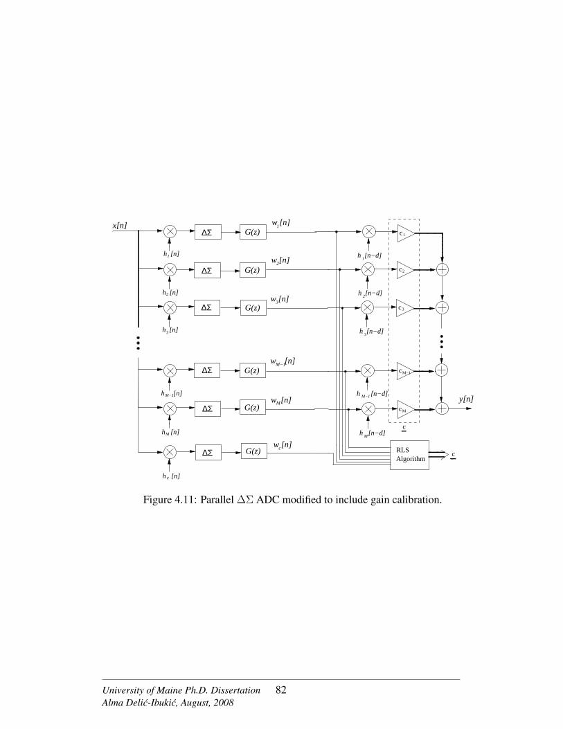
c
c
G(z)
G(z)
G(z)
G(z)
G(z)
G(z)w [n]c
Mw [n]
M−1w [n]
3w [n]
w [n]2
w [n]1
M−1
c
1
2
3
M−1
M
c
c
c
c
c
M
AlgorithmRLS
M
3
2
1
h [n]
h [n]
h [n]
h [n]
3h [n−d]
2h [n−d]
1h [n−d]
y[n]
h [n−d]
M−1
x[n]
h [n]
h [n]
h [n−d]
∆Σ
∆Σ
∆Σ
∆Σ
∆Σ
∆Σ
Figure 4.11: Parallel ∆Σ ADC modified to include gain calibration.
University of Maine Ph.D. DissertationAlma Delic-Ibukic, August, 2008
82

The ∆Σ modulator output contains two terms: the delayed version of the input sig-
nal X(z) and quantization error E(z) that is modified by the noise transfer function
NTF (z).
Quantization error was discussed in Section 2.4.1. It was modelled as an addi-
tive white noise source e[n] with samples uniformly distributed within ±QB/2 interval,
where QB is the quantization interval and B is the resolution of the quantizer. If a ∆Σ
modulator is used, quantization error is further modified by noise shaping filterNTF (z)
whose general form is given in (4.29). The two together form the quantization noise that
is seen at the output of ∆Σ modulators.
Figure 4.12 shows a Nyquist rate Π∆Σ converter modified to include continuous
gain calibration algorithm and filtered quantization noise vr[n]. Before demodulation,
the outputs of all channels are routed to an adaptive filter algorithm for finding a least
squares solution recursively [81]. The result is then scaled by the known 1/αr values for
r = 1, 2, ...,M to obtain gain correction terms for each channel, cr = βr/αr. Filtered
quantization noise vr[n] is part of the input to an adaptive filter algorithm and therefore
its impact on the overall algorithm performance must be examined. Π∆Σ architecture
converters contain M identical channels, so each channel contributes the same amount
of filtered quantization noise power to an adaptive filter algorithm and the overall con-
verter output y[n]. The amount of filtered quantization noise power that is seen at the
output of each channel is given by
σ2v =
2Q2B
12
∫ 12
0
∣∣NTF (ej2πf )G(ej2πf )∣∣2 df
=Q2B
6
∫ 12
0
(2 sinπf)2L∣∣G(ej2πf )
∣∣2 df (4.30)
whereQ2B/12 is the quantization error power that was derived in Section 2.4.2. NTF (ej2πf )
and G(ej2πf ) are the frequency responses of the noise shaping filter and the lowpass fil-
ter, respectively.
University of Maine Ph.D. DissertationAlma Delic-Ibukic, August, 2008
83

c
c
G(z)
G(z)
G(z)
G(z)
G(z)
G(z)w [n]c
Mw [n]
M−1w [n]
v [n]c
v [n]M
v [n]M−1
3w [n]
w [n]2
w [n]1
3v [n]
2v [n]
v [n]1
M−1
c
1
2
3
M−1
M
c
c
c
c
c
M
AlgorithmRLS
M
3
2
1
h [n]
h [n]
h [n]
h [n]
3h [n−d]
2h [n−d]
1h [n−d]
y[n]
h [n−d]
M−1
x[n]
h [n]
h [n]
h [n−d]
∆Σ
∆Σ
∆Σ
∆Σ
∆Σ
∆Σ
Figure 4.12: Parallel ∆Σ ADC modified to include gain calibration and filtered quanti-zation noise vr[n].
University of Maine Ph.D. DissertationAlma Delic-Ibukic, August, 2008
84
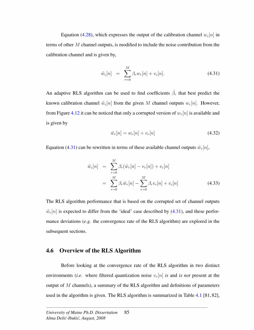
Equation (4.28), which expresses the output of the calibration channel wc[n] in
terms of other M channel outputs, is modified to include the noise contribution from the
calibration channel and is given by,
wc[n] =M∑r=0
βrwr[n] + vc[n]. (4.31)
An adaptive RLS algorithm can be used to find coefficients βr that best predict the
known calibration channel wc[n] from the given M channel outputs wr[n]. However,
from Figure 4.12 it can be noticed that only a corrupted version of wr[n] is available and
is given by
wr[n] = wr[n] + vr[n] (4.32)
Equation (4.31) can be rewritten in terms of these available channel outputs wr[n],
wc[n] =M∑r=0
βr(wr[n]− vr[n]) + vc[n]
=M∑r=0
βrwr[n]−M∑r=0
βrvr[n] + vc[n] (4.33)
The RLS algorithm performance that is based on the corrupted set of channel outputs
wr[n] is expected to differ from the ‘ideal’ case described by (4.31), and these perfor-
mance deviations (e.g. the convergence rate of the RLS algorithm) are explored in the
subsequent sections.
4.6 Overview of the RLS Algorithm
Before looking at the convergence rate of the RLS algorithm in two distinct
environments (i.e. where filtered quantization noise vr[n] is and is not present at the
output of M channels), a summary of the RLS algorithm and definitions of parameters
used in the algorithm is given. The RLS algorithm is summarized in Table 4.1 [81, 82],
University of Maine Ph.D. DissertationAlma Delic-Ibukic, August, 2008
85
Initialize the algorithm by settingP [0] = δ−1I , where δ is a small positive constantβ[0] = α
For each training epoch n = 1, 2, 3, ..., compute
k[n] =P [n− 1]w[n]
λ+ wT [n]P [n− 1]w[n]
ξ[n] = wc[n]− βT [n− 1]w[n]
β[n] = β[n− 1] + k[n]ξ[n]
P [n] = λ−1(P [n− 1]− k[n]wT [n]P [n− 1]
)Table 4.1: Summary of the RLS algorithm
where w[n] is a vector defined by
w[n] = [w0[n], w1[n], w2[n], ..., wM [n]]T (4.34)
with each element described by (4.32). The first element w0[n] is always 1, and wr[n]
for r = 1, 2, ...,M are outputs of M channels at time n (i.e. RLS algorithm training
samples). The vector β[n] is a vector of estimated coefficients at training instant n that
best fit the solution to (4.33). It is defined as
β[n] = [β0[n], β1[n], β2[n], ..., βM [n]]T . (4.35)
The initialization vector α is the vector of known coefficients that are used to find the
modulation sequence of the calibration channel hc[n]. By design,α is composed of only
±1’s as defined in (4.22).
α = [α0, α1, α2, α3, ..., αM ]T (4.36)
University of Maine Ph.D. DissertationAlma Delic-Ibukic, August, 2008
86

The first element α0 should be initialized to zero to reflect the design goal of zero DC
offset in all channels. The other M elements of α are found according to (4.22). The
term λ is a positive scalar that is equal to, or is close to 1, and is also known as a
forgetting factor [81, 82]. If λ = 1, then all the past data is contributed in computing
the updated coefficient vector β. On the other hand, if λ < 1, then the past data values
are attenuated exponentially while the importance in computing updated coefficients is
given to more recent data samples. The forgetting factor allows for the RLS algorithm
to run in nonstationary environment. The matrix P [n] = Φ−1[n] is the inverse of an
(M + 1) × (M + 1) correlation matrix Φ[n], where Φ[n] is a correlation matrix of the
RLS algorithm inputs w[n] at training sample n. The correlation matrix Φ[n] is defined
by
Φ[n] =n∑i=1
λn−iw[n]wT [n] (4.37)
A positive constant δ is required for the initialization of matrix P [n]. It should be
selected such that it is small compared to 0.01σ2w, where σ2
w is the variance of training
samples w[n] [82].
In the absence of quantization noise vr[n] in the channels, (w[n] = w[n]), (4.31)
becomes a classic linear least squares problem, and the RLS algorithm of Table 4.1 can
be shown to converge to the least-squares solution.
To analyze the quality of the RLS algorithm solution, an analytical measure of
the accuracy of the coefficients estimation is used [82–84] which is given by
Q[n] = E
(M∑r=0
(βr[n]− βr)2
)= E
((β[n]− β)T (β[n]− β)
)(4.38)
where β is a vector of true coefficients, β[n] is a vector of estimated coefficients at
University of Maine Ph.D. DissertationAlma Delic-Ibukic, August, 2008
87
training instant n. Term (β[n]− β) is the coefficient error vector [82] and is defined as
β[n]− β = Φ−1[n]n∑i=1
w[i]vc[i] (4.39)
where vc[n] is filtered quantization noise contribution from the calibration channel wc[n].
For the case when w[n] = w[n], this is the only noise contribution to the RLS algorithm.
The RLS algorithm can be shown to converge under two common assumptions [82]:
Assumption-1: The input vectors w[n], for n = 1, 2, 3, ... are independently and identi-
cally distributed.
Assumption-2: The input vectors w[n], for n = 1, 2, 3, ... are drawn from a stochas-
tic process with a multivariate Gaussian distribution of zero mean and
ensemble-averaged correlation matrixR = limn→∞
1
nΦ[n].
Based on these assumptions, in [82, 83] RLS algorithm performance is given by
Q[n] =M
n
σ2v
σ2w
n�M + 1 (4.40)
where n is a training instant, M is the number of channels in a parallel configuration,
σ2v is the filtered quantization noise power for calibration channel wc[n] given by (4.30),
and σ2w is the signal power seen at the output of a single Π∆Σ channel before demodula-
tion. In (4.40), filtered quantization noise power σ2v and the number of parallel channels
M are fixed quantities that are determined by the overall design of Π∆Σ ADC. There-
fore, the two parameters that can be modified are the number of training samples n
and the RLS algorithm input signal power σ2w. Based on the relationship in (4.40), a
faster convergence rate for the RLS algorithm requires larger σ2w. This implies that for
a given number of training samples, there is always a minimum requirement placed on
the variance of the RLS algorithm training samples σ2w.
The above discussion focused on the RLS algorithm performance when finding
University of Maine Ph.D. DissertationAlma Delic-Ibukic, August, 2008
88

coefficients β that best predict solution to (4.31). As discussed in Section 4.5, only a
corrupted version of wr[n] is available, namely wr[n] = wr[n] + vr[n] where vr[n] is
filtered quantization noise seen at the output of the rth channel of Π∆Σ ADC. The fol-
lowing section examines the effect of the filtered quantization noise on the performance
of the RLS algorithm.
4.7 The RLS Algorithm Applied to Π∆Σ ADCs
To analyze the performance of the RLS algorithm in the presence of the filtered
quantization noise, the coefficient error vector described in (4.39) needs to be examined.
If the filtered quantization noise vr[n] were not present in the rth channel of an
M channel Π∆Σ converter, the coefficient error vector would have the following form
β[n]− β = Φ−1[n]n∑i=1
w[i]vc[i] (4.41)
where
Φ[n] =n∑i=1
w[n]wT [n] (4.42)
The expected value of the coefficient error vector E(β[n] − β) would be zero because
the quantization noise in the calibration channel vc[n] and the rth channel output wr[n]
are independent of each other. This implies that the RLS algorithm converges in the
mean for training samples n ≥M to the optimum coefficients β,
E(β[n]) = β, n ≥M. (4.43)
With the quantization noise taken into account, coefficients β that best predict
the solution to (4.33) are sought. In this case the coefficient error vector becomes
β[n]− β = Φ−1[n]n∑i=1
w[i](vc[i]− βTv[i]) (4.44)
University of Maine Ph.D. DissertationAlma Delic-Ibukic, August, 2008
89
where Φ[n] is given by (4.37) with a forgetting factor λ set to 1, w[n] = w[n]+v[n] and
v[n] = [v0[n], v1[n], v2[n], ..., vM [n]]T is the filtered quantization noise vector. The first
element of v[n] is always zero and vr[n] for r = 1, 2, ...,M is filtered quantization noise
for the rth channel in Π∆Σ architecture with variance σ2v given by (4.30). To simplify
the analysis of the RLS algorithm performance in the presence of filtered quantization
noise, the correlation matrix Φ[n] is approximated by
Φ[n] =n∑i=1
w[i]wT [i]
=n∑i=1
(w[i] + v[i])(w[i] + v[i])T
=n∑i=1
w[i]wT [i] +n∑i=1
w[i]vT [i] +n∑i=1
v[i]wT [i] +n∑i=1
v[i]vT [i]
∼= Φ[n] (4.45)
Equation (4.44) can be written in terms of Φ[n], w[n] and v[n],
β[n]− β = Φ−1[n]n∑i=1
(w[i] + v[i])(vc[i]− βTv[i]) (4.46)
= Φ−1[n]
(n∑i=1
w[i](vc[i]− βTv[i]) +n∑i=1
v[i](vc[i]− βTv[i])
)
= Φ−1[n]
(n∑i=1
w[i](vc[i]− βTv[i]) +n∑i=1
v[i]vc[i]−n∑i=1
v[i]βTv[i]
)
The expected value of the coefficient error vector in (4.46) does not converge to a zero,
instead it converges to a bias that depends on the variance of the filtered quantization
noise σ2v , and inverse of the correlation matrix Φ−1[n] of the input vector w[n]. The
University of Maine Ph.D. DissertationAlma Delic-Ibukic, August, 2008
90

expectation for the coefficient error vector in (4.46) is given by
E(β[n]− β) = −E
(Φ−1[n]
n∑i=1
v[i]v[i]Tβ
)
= −E
(Φ−1[n]
n∑i=1
σ2vIβ
)= −nσ2
vE(Φ−1[n])β (4.47)
where n is a training instant and β are the optimum coefficients that best predict the
solution to (4.33). The expected value of the first two terms in (4.46) are zero because
random variables in question are independent of each other.
In [82] it was shown that the expectation of the inverse correlation matrix Φ−1[n]
is exactly
E(Φ−1[n]) =1
n−M − 1R−1, n > M + 1 (4.48)
where n is a training instant, M is the number of channels in parallel configuration and
R is ensemble-averaged correlation matrix of the RLS algorithm input vectorw[n]. Be-
cause input vectorsw[n] for n = 1, 2, 3, ... are independently and identically distributed,
as stated on page 88, the ensemble-averaged correlation matrix R = σ2wI , where σ2
w is
the variance of the input vector w[n] and I is M by M identity matrix. For training
samples n�M + 1, (4.47) can be further simplified to
E(β[n]− β) = −σ2vR−1β
= − σ2v
σ2w
β (4.49)
Equation (4.49) states that the RLS algorithm in the presence of the filtered quantization
noise converges in the mean for training samples n�M+1 to the optimum coefficients
University of Maine Ph.D. DissertationAlma Delic-Ibukic, August, 2008
91

β plus a bias term,
E(β[n]) = β − σ2v
σ2w
β
= β
(1− σ2
v
σ2w
), n�M + 1 (4.50)
For the RLS algorithm to converge to the optimum filter coefficients β, the biasing
constant σ2v/σ
2w must be small, which implies that signal to noise ratio at the output of
the rth channel of an M channel Π∆Σ converter needs to be large. The biasing term
in (4.50) is independent of the number of training samples n, therefore the RLS algo-
rithm convergence in the mean can only improve by increasing the variance of training
samples w[n] or reducing quantization noise v[n]. Reducing quantization noise in a
given channel is not an option, because quantization noise is inherent to A/D converter
architectures and it is determined by the overall design of Π∆Σ ADC. Therefore, the
only way to improve the RLS algorithm convergence in the mean is by increasing the
variance of training samples σ2w.
The biasing term in (4.49) directly affects the performance measure Q[n] of the
RLS algorithm given in (4.38) by introducing an offset in the solution. Q[n] in the
presence of the filtered quantization noise is derived next. The derivation is based on the
analysis done in [82] and assumptions listed on page 88.
The coefficient error vector in the presence of quantization noise was given in
(4.46), and its correlation matrix is defined here as
K[n] = E(
(β[n]− β)(β[n]− β)T)
(4.51)
= E
(Φ−1[n]
n∑i=1
n∑j=1
w[i](vc[i]− βTv[i])(vc[j]− βTv[j])T wT [j]Φ−1[n]
)
University of Maine Ph.D. DissertationAlma Delic-Ibukic, August, 2008
92

where w[n] = w[n] + v[n]. Writing (4.51) in terms w[n] and v[n],
K[n] = E
(Φ−1[n]
n∑i=1
n∑j=1
w[i](vc[i]− βTv[i])(vc[j]− βTv[j])TwT [j]Φ−1[n]
)
+ E
(Φ−1[n]
n∑i=1
n∑j=1
v[i](vc[i]− βTv[i])(vc[j]− βTv[j])TvT [j]Φ−1[n]
)(4.52)
By invoking the expectation property of a random variable E(X) = E(E(X|Y = y)),
where E(X|Y = y) is a conditional expectation of X given a value Y = y, (4.51) can
be rewritten given a vector w[i], i = 1, 2, 3, ..., n, as
K[n] = E
(Φ−1[n]
n∑i=1
n∑j=1
w[i]E((vc[i]− βTv[i])(vc[j]− βTv[j])T
)wT [j]Φ−1[n]
)
+ E
(Φ−1[n]
n∑i=1
n∑j=1
E(v[i](vc[i]− βTv[i])(vc[j]− βTv[j])TvT [j]
)Φ−1[n]
)(4.53)
Each of the two expectation terms in (4.53) will be analyzed separately. Filtered
quantization noise v[n] and vc[n] that is encountered in each of the M channels of Π∆Σ
ADC and calibration channel, respectively, is modelled as an additive white noise pro-
cess with variance σ2v . The expectation of the filtered quantization noise of the first term
in (4.53) can be simplified to
E((vc[i]− βTv[i])(vc[j]− βTv[j])T
)=
E (vc[i]vc[j]) + E(βTv[i]vT [j]β
)=
2σ2v , i = j
0, i 6= j(4.54)
where coefficients β = αa/ac and βTβ ∼= 1. Vectorα is defined in (4.36) and is a vec-
tor of known coefficients that allows for a modulation sequence of calibration channel
University of Maine Ph.D. DissertationAlma Delic-Ibukic, August, 2008
93

to be composed of only ±1 terms. Terms a = 1 + ε and ac = 1 + εc are the vector of
gain errors in each of the M channels and in the calibration channel, respectively.
The expectation of the filtered quantization noise of the second term in (4.53)
can be simplified to
n∑i=1
n∑j=1
E(v[i](vc[i]− βTv[i])(vc[j]− βTv[j])TvT [j]
)=
n∑i=1
n∑j=1
E(v[i]βTv[i]vT [j]βvT [j]
)=
3nσ4vββ
T , i = j
n(n− 1)σ4vββ
T , i 6= j(4.55)
For the case when i = j, the fourth order moment for a normal random variable is
used [85], otherwise random variables v[i] and v[j] are independent of each other. With
the above simplifications, (4.53) can be written in terms of (4.42), (4.54)and (4.55),
K[n] = 2σ2vE
(Φ−1[n]
n∑i=1
w[i]wT [i]Φ−1[n]
)+E
(Φ−1[n]Φ−1[n]
) (n2σ4
v + 2nσ4v
)ββT
= 2σ2vE(Φ−1[n]Φ[n]Φ−1[n]
)+ E
(Φ−1[n]Φ−1[n]
) (n2σ4
v + 2nσ4v
)ββT
= 2σ2vE(Φ−1[n]
)+ E
(Φ−1[n]Φ−1[n]
) (n2σ4
v + 2nσ4v
)ββT (4.56)
For training samples n�M + 1, (4.56) can be further simplified in terms of (4.48),
K[n] =2σ2
v
nR−1 + E
(Φ−1[n]Φ−1[n]
) (n2σ4
v + 2nσ4v
)ββT (4.57)
where R is the ensemble-averaged correlation matrix of the input w[n]. Behavior of
the second term in (4.57) is an offset contribution that can be analyzed in terms of the
ensemble-averaged correlation matrix R. The ensemble-averaged correlation matrix R
is given as
R = limn→∞
1
nΦ[n] (4.58)
University of Maine Ph.D. DissertationAlma Delic-Ibukic, August, 2008
94
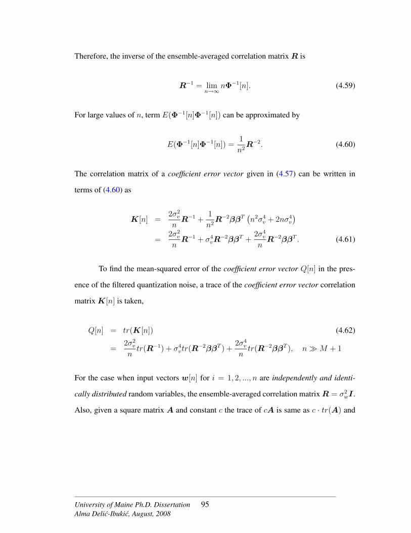
Therefore, the inverse of the ensemble-averaged correlation matrixR is
R−1 = limn→∞
nΦ−1[n]. (4.59)
For large values of n, term E(Φ−1[n]Φ−1[n]) can be approximated by
E(Φ−1[n]Φ−1[n]) =1
n2R−2. (4.60)
The correlation matrix of a coefficient error vector given in (4.57) can be written in
terms of (4.60) as
K[n] =2σ2
v
nR−1 +
1
n2R−2ββT
(n2σ4
v + 2nσ4v
)=
2σ2v
nR−1 + σ4
vR−2ββT +
2σ4v
nR−2ββT . (4.61)
To find the mean-squared error of the coefficient error vector Q[n] in the pres-
ence of the filtered quantization noise, a trace of the coefficient error vector correlation
matrixK[n] is taken,
Q[n] = tr(K[n]) (4.62)
=2σ2
v
ntr(R−1) + σ4
vtr(R−2ββT ) +
2σ4v
ntr(R−2ββT ), n�M + 1
For the case when input vectors w[n] for i = 1, 2, ..., n are independently and identi-
cally distributed random variables, the ensemble-averaged correlation matrixR = σ2wI .
Also, given a square matrix A and constant c the trace of cA is same as c · tr(A) and
University of Maine Ph.D. DissertationAlma Delic-Ibukic, August, 2008
95

RLS algorithm
RLS algorithm
withnoise
E(β[n]− β) 0 − σ2v
σ2w
β
Q[n] = E(
(β[n]− β)T (β[n]− β)) M
n
σ2v
σ2w
M
n
2σ2v
σ2w
+
(σ2v
σ2w
)2
Table 4.2: Summary of the RLS algorithm convergence for n�M+1 with and withoutquantization noise present.
therefore (4.62) can be simplified to
Q[n] =M
n
2σ2v
σ2w
+σ4v
σ4w
tr(ββT ) +1
n
2σ4v
σ4w
tr(ββT )
=M
n
2σ2v
σ2w
+σ4v
σ4w
+1
n
2σ4v
σ4w
∼=M
n
2σ2v
σ2w
+σ4v
σ4w
(4.63)
where training samples n � M + 1 and tr(ββT ) ∼= 1. Equation (4.63) shows that the
RLS algorithm performance in the presence of filtered quantization noise is limited by
the offset term σ4v/σ
4w. The offset term is independent of the number of training samples
n. If a desired accuracy of the coefficients estimation is required (i.e. Q[n]), the offset
term must be bounded to at least the required accuracy. The offset term depends on
two quantities, namely quantization noise power σ2v and the RLS algorithm input signal
power σ2w. Table 4.2 gives a summary of the RLS algorithm convergence results in the
presence of the quantization noise.
As mentioned before, the quantization noise power in a single channel of a Π∆Σ
ADC is a fixed quantity that depends on the design of the overall system, so the only
parameter that can be modified is the RLS algorithm input signal power σ2w. Putting an
upper bound on the offset term in (4.63) places a minimum requirement on the input
University of Maine Ph.D. DissertationAlma Delic-Ibukic, August, 2008
96

signal power σ2w. This in turn determines the length of data required to achieve the
desired accuracy.
4.8 Simulation Results for the RLS Algorithm Performance
To verify the quality and the convergence rate of the RLS algorithm, an 8-
channel oversampling Π∆Σ converter with an additional channel for calibration was
modelled in MATLAB in which each channel contains 2nd order ∆Σ modulators with a
1-bit quantizer and decimation filter described by (4.15). The 1-bit quantizer was mod-
elled as an additive white noise source, and the oversampling ratio of D = 4 was used
in simulations.
As discussed in Section 4.4, known coefficients αr, where r = 1, 2, ..., 8, need to
be selected so the modulation sequence hc[n] for the calibration channel contains only
±1 terms. Coefficients αr should preferably have equal magnitude, so each channel in
the Π∆Σ architecture is given equal importance. For the case of an 8-channel Π∆Σ
converter, coefficients αr of equal magnitude do not exist. As identified by a computer
search algorithm, one of the valid solutions for coefficients αr that yielded only ±1
terms for a modulation sequence hc[n], was
α = [0.25 0.25 −0.25 −0.25 0.25 −0.75 −0.25 −0.25]T
The RLS algorithm performance analysis was based on the assumptions listed on page 88.
To effectively compare simulation results with theory, the Π∆Σ ADC input signal sam-
ples x[n] were taken from a normal distribution with zero mean and variance σ2x. For
the oversampling Π∆Σ ADC, the variance seen at the output of each channel of an
M -channel Π∆Σ converter before demodulation is given by
σ2w = σ2
x
∞∑n=0
|g[n]|2 (4.64)
University of Maine Ph.D. DissertationAlma Delic-Ibukic, August, 2008
97

where g[n] is the impulse response of a lowpass decimation filter described by (4.12) and
discussed in Section 4.2.1. For the modelled 8-channel Π∆Σ ADC, with oversampling
ratio D = 4 and decimation filter described by (4.15), the variance seen at the output of
each channel is
σ2w∼= (0.0172)σ2
x. (4.65)
The RLS algorithm performance was analyzed in terms of the mean-square error
of the coefficient error vector Q[n] that is given by (4.38). Two sets of analysis were
conducted: the RLS algorithm solution to (4.31), where the algorithm’s input signal
w[n] = w[n], and the RLS algorithm solution to (4.33), where the algorithm’s input
signal is corrupted by noise, w[n] = w[n] +v[n]. The behavior of the measure Q[n] for
the RLS algorithm performance when w[n] = w[n] is given by (4.40) and is repeated
here in a decibel form
Q[n]dB = 10 log10
(M
n
)− 10 log10
(σ2w
σ2v
), n�M + 1 (4.66)
whereσ2w
σ2v
is known as a signal-to-noise ratio. The metric Q[n] for the RLS algorithm
performance when w[n] = w[n] + v[n] is given by (4.63). Except for the factor of 2
that modifies the amount of quantization noise seen in the RLS algorithm, the algorithm
follows the convergence rate of (4.66) until the offset termσ4v
σ4w
starts to dominate.
Figure 4.13 shows the RLS algorithm performance in terms of Q[n]dB for a
simulated 8-channel Π∆Σ converter plus an additional channel for calibration and a
signal-to-noise ratio of 30 dB and 40 dB. The quantization noise power σ2v was found
according to (4.30) and a gain error mismatch of 1% was simulated and introduced to
all eight channels. The variance at the converter input σ2x was found based on the given
signal-to-noise ratio σ2w/σ
2v and (4.65). Coefficients β[n] that contain gain correction
terms and are used in determining Q[n], are found using the RLS algorithm described
in Table 4.1. The results shown in Figure 4.13 are averaged over 10 simulation runs.
University of Maine Ph.D. DissertationAlma Delic-Ibukic, August, 2008
98

102 103 104 105 106−80
−75
−70
−65
−60
−55
−50
−45
−40
−35
−30
Training samples
Q[n
] in
dB
Expected performanceRLS algorithm convergenceRLS algorithm convergence with noise
(a) Signal-to-noise ratio is 30 dB.
102 103 104 105 106−90
−85
−80
−75
−70
−65
−60
−55
−50
−45
−40
Training samples
Q[n
] in
dB
Expected performanceRLS algorithm convergenceRLS algorithm convergence with noise
(b) Signal-to-noise ratio is 40 dB.
Figure 4.13: The RLS algorithm performance and convergence results for an 8-channelΠ∆Σ converter with the oversampling rate D = 4.
University of Maine Ph.D. DissertationAlma Delic-Ibukic, August, 2008
99

Curves show the expected convergence of Q[n]dB as predicted by (4.66), and the RLS
algorithm performance with and without quantization noise v[n].
The RLS algorithm performance without quantization noise was simulated by
modelling an ideal 2nd order ∆Σ modulator without a quantizer (i.e. the quantizer is
assumed to be ideal with infinite resolution). Results in Figure 4.13 deviate from what
is expected in theory. The algorithm appears to be converge faster than expected when
implemented in the described environment. By assuming an ideal quantizer, the RLS
algorithm was expected to agree with the theoretical convergence curve described by
(4.66). Also, the RLS algorithm performance with quantization noise was expected to
be 3 dB worse than the theoretical convergence curve given by (4.66), due to the factor
of two that is present in (4.63). On the other hand, the presence of the offset term in
(4.63) is in the agreement with what is seen in simulation results. Because the offset
termσ4v
σ4w
in (4.63) depends on the RLS algorithm input signal and filtered quantization
noise power, the Q[n]dB stops converging according to (4.66) once it reaches -60 dB
when signal-to-noise ratio of 30 dB is used, and -80 dB when signal-to-noise ratio of
40 dB is used. Therefore, once the offset term is reached, further training does not
improve the mean-square error of the coefficient error vector Q[n].
Deviations of the RLS algorithm performance from the theory summarized in
Table 4.2 are attributed to the assumptions made when the theory was derived. The
theory is based on the assumptions that both the training samples w[n] and filtered
quantization noise v[n] have flat power spectral densities. Implementation of the ∆Σ
modulator and decimation filter introduces spectral shaping to the signal path and noise
path. As discussed in Section 2.4.3, the quantization noise in ∆Σ modulators get pushed
out of the signal band of interest to high frequencies where it will be filtered out. Sim-
ilarly, only the desired signal bandwidth is passed through the filter. There is a portion
of frequency spectrum where signal-to-noise ratio is better than theory predicts. This
spectral shaping has a positive effect on the convergence of the RLS algorithm.
University of Maine Ph.D. DissertationAlma Delic-Ibukic, August, 2008
100

To confirm this, an 8-channel converter set up with an additional channel for
calibration was modelled in MATLAB where the ∆Σ modulator and decimation filter
were excluded from the channel. This model matches the assumption used to derive
theory in Sections 4.6 and 4.7. Quantization noise v[n] and input signal samples x[n]
were taken from a normal distribution with zero mean and variance σ2v and σ2
x, respec-
tively. The quantization noise power σ2v was found according to (4.30). Because the ∆Σ
modulator and decimation filter are not included in the simulation run, the signal power
at the output of each channel before demodulation is σ2w = σ2
x. Also, the gain error mis-
matches of 1% were simulated and introduced in all eight channels. Figure 4.14 shows
the simulated RLS algorithm performance in terms of QdB[n] for this case and signal-
to-noise ratios of 30 dB and 40 dB. Plotted results are averaged over 10 simulation runs.
Curves show the expected convergence as predicted by (4.66), and the RLS algorithm
performance with and without quantization noise v[n]. As anticipated, when quantiza-
tion noise is introduced only to the calibration channel, the RLS algorithm behaves as
predicted by (4.66). Also, when quantization noise is introduced to all channels, the
RLS algorithm follows the convergence trend of (4.66) (plus the 3 dB offset described
earlier) until the offset term σ4v/σ
4w in (4.63) starts to dominate.
To see the effect of limited convergence of Q[n] on coefficients β[n], the RLS
convergence in the mean is examined. In Section 4.7 it was shown that the RLS algo-
rithm applied to Π∆Σ converters converges in the mean to
E(β[n]) = β − σ2v
σ2w
β, n�M + 1. (4.67)
Ideally, β[n] should converge in the mean to true coefficients β. Figures 4.15 and 4.16
show the convergence of two coefficients (β2[n]) and β6[n], for a simulated 8-channel
Π∆Σ ADC with signal-to-noise ratio of 30 dB and gain mismatch errors of 1% intro-
duced in all eight channels. As before, the estimated coefficients β[n] are found using
University of Maine Ph.D. DissertationAlma Delic-Ibukic, August, 2008
101

102 103 104 105 106−80
−75
−70
−65
−60
−55
−50
−45
−40
−35
−30
Training samples
Q[n
] in
dB
Expected performanceRLS algorithm convergenceRLS algorithm convergence with noise
(a) Signal-to-noise ratio is 30 dB.
102 103 104 105 106−90
−85
−80
−75
−70
−65
−60
−55
−50
−45
−40
Training samples
Q[n
] in
dB
Expected performanceRLS algorithm convergenceRLS algorithm convergence with noise
(b) Signal-to-noise ratio is 40 dB.
Figure 4.14: The RLS algorithm performance and convergence results for an 8-channelset up where ∆Σ modulator and decimation filter were taken out of a channel path.
University of Maine Ph.D. DissertationAlma Delic-Ibukic, August, 2008
102

102
103
104
105
106
0.25
0.252
0.254
0.256
0.258
0.26(a)
Coe
ffici
ent
β2[n
]
102
103
104
105
106
0.24
0.245
0.25
0.255
Training samples
Coe
ffici
ent
β2[n
]
(b)
Figure 4.15: Convergence of the coefficient β2[n]: (a) ideal case, quantization noiseat the output of each channel is excluded and (b) RLS algorithm performance in thepresence of the quantization noise. Solid lines designate the optimum coefficients β,and the dashed lines designate the optimum coefficients β with the offset term included.
University of Maine Ph.D. DissertationAlma Delic-Ibukic, August, 2008
103
102
103
104
105
106
−0.756
−0.754
−0.752
−0.75
−0.748(a)
Coe
ffici
ent
β6[n
]
102
103
104
105
106
−0.755
−0.75
−0.745
−0.74
−0.735(b)
Coe
ffici
ent
β6[n
]
Training samples
Figure 4.16: Convergence of the coefficient β6[n]: (a) ideal case, quantization noiseat the output of each channel is excluded and (b) RLS algorithm performance in thepresence of the quantization noise. Solid lines designate the optimum coefficients β,and the dashed lines designate the optimum coefficients β with the offset term included.
University of Maine Ph.D. DissertationAlma Delic-Ibukic, August, 2008
104

an RLS algorithm described in Table 4.1 and the results are based on a single simula-
tion run. Solid lines designate the optimum coefficients β, and dashed lines designate
the optimum coefficients β with the offset term included. In both figures, the two co-
efficients converge as excepted by (4.67) to the offset termσ2v
σ2w
β. Also, the offset is
more pronounced for β6[n]. Coefficient terms β[n] are proportional to the coefficients
α which determine the modulation sequence hc[n] for calibration channel. In the case
of an 8-channel Π∆Σ ADC, coefficients α of equal magnitude are unattainable leaving
one term with a dominant magnitude (i.e. α6). Coefficient α6 will increase the offset
term in (4.67), causing coefficient β6 to deviate more from the desired value β6. It is
apparent from (4.67) that by increasing signal-to-noise ratio, the offset term decreases
which allows for more accurate estimation of coefficients β[n].
4.9 Calibration Algorithm and Dynamic Range Improvement
Channel gain errors and their locations in the frequency spectrum of Π∆Σ ADCs
were discussed in Section 4.3. The unwanted frequency tones degrade the overall perfor-
mance (i.e. dynamic range) of Π∆Σ converters. To quantitatively relate the accuracy of
the developed calibration algorithm to improvements in the dynamic range of the Π∆Σ
converter requires knowledge of the peak frequency tone levels that can be generated by
a given gain error.
If a full scale sinusoidal input signal is applied to an M channel time-interleaved
converter, the mean and variance of error tones due to channel gain mismatches are
given by [70]
µg =σa2
√π
M
σ2g = (1− π/4)
σ2a
M(4.68)
where σ2a is the variance of a total gain in a channel ar for r = 1, 2, ...,M with M being
University of Maine Ph.D. DissertationAlma Delic-Ibukic, August, 2008
105
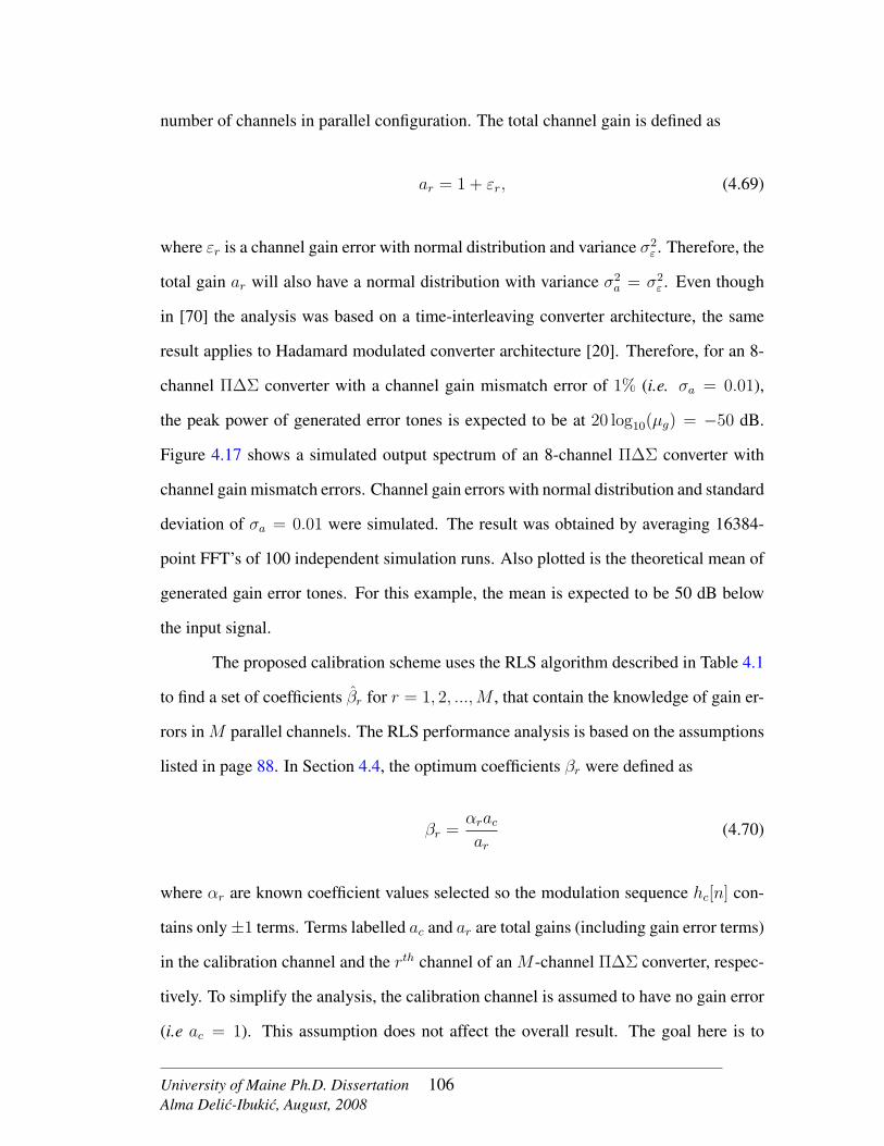
number of channels in parallel configuration. The total channel gain is defined as
ar = 1 + εr, (4.69)
where εr is a channel gain error with normal distribution and variance σ2ε . Therefore, the
total gain ar will also have a normal distribution with variance σ2a = σ2
ε . Even though
in [70] the analysis was based on a time-interleaving converter architecture, the same
result applies to Hadamard modulated converter architecture [20]. Therefore, for an 8-
channel Π∆Σ converter with a channel gain mismatch error of 1% (i.e. σa = 0.01),
the peak power of generated error tones is expected to be at 20 log10(µg) = −50 dB.
Figure 4.17 shows a simulated output spectrum of an 8-channel Π∆Σ converter with
channel gain mismatch errors. Channel gain errors with normal distribution and standard
deviation of σa = 0.01 were simulated. The result was obtained by averaging 16384-
point FFT’s of 100 independent simulation runs. Also plotted is the theoretical mean of
generated gain error tones. For this example, the mean is expected to be 50 dB below
the input signal.
The proposed calibration scheme uses the RLS algorithm described in Table 4.1
to find a set of coefficients βr for r = 1, 2, ...,M , that contain the knowledge of gain er-
rors in M parallel channels. The RLS performance analysis is based on the assumptions
listed in page 88. In Section 4.4, the optimum coefficients βr were defined as
βr =αracar
(4.70)
where αr are known coefficient values selected so the modulation sequence hc[n] con-
tains only±1 terms. Terms labelled ac and ar are total gains (including gain error terms)
in the calibration channel and the rth channel of an M -channel Π∆Σ converter, respec-
tively. To simplify the analysis, the calibration channel is assumed to have no gain error
(i.e ac = 1). This assumption does not affect the overall result. The goal here is to
University of Maine Ph.D. DissertationAlma Delic-Ibukic, August, 2008
106

0 0.05 0.1 0.15 0.2 0.25 0.3 0.35 0.4 0.45 0.5−140
−120
−100
−80
−60
−40
−20
0
Normalized Frequency
Mag
nitu
de, d
BFS
Figure 4.17: Averaged output spectrum for an 8-channel Π∆Σ converter with a 1%channel gain mismatch error and oversampling ratio D = 4. The dashed line corre-sponds to theoretical mean of spectral peaks caused by channel gain mismatches.
find channel mismatches, and if there is a gain error present in the calibration channel,
than all the channels will be calibrated with respect to gain ac of the calibration channel.
Setting ac = 1 and writing (4.70) in terms of the RLS algorithm coefficient estimates
βr[n] leads to the following expression
βr[n] =αrar
+ εβ[n] (4.71)
where εβ[n] is the error describing deviation of βr[n] from the optimum solution βr at
training instant n.
Equation (4.71) shows that the estimated coefficients βr[n] are inversely propor-
tional to the total gain ar in a given channel. Dividing βr[n] by the known value of αr
and scaling the output of the rth channel by this new expression will correct for channel
University of Maine Ph.D. DissertationAlma Delic-Ibukic, August, 2008
107

gain mismatches. The new expression for the gain that is contained in each channel is
ar[n] = ar
(αrar
+ εβ[n]
)1
αr
= 1 +arεβ[n]
αr
= 1 +(1 + εr)εβ[n]
αr
∼= 1 +εβ[n]
αr(4.72)
The error term εβ[n] depends on the accuracy of estimation of βr[n], which in turn
depends on the RLS algorithm performance. The RLS performance was analyzed in
terms of a mean-square error of coefficient error vector Q[n] that is given in (4.38). Q[n]
can be also interpreted as a sum of variances of εβ[n] that is contained in M channels.
Therefore, the variance of the error describing the deviation of βr[n] from the optimum
solution βr at the training instant n is
σ2εβ
=Q[n]
M, (4.73)
where M is the number of channels in parallel configuration. Based on (4.73), the new
gain ar[n] in (4.72) has a variance
σ2a =
Q[n]
Mα2r
. (4.74)
Equation (4.74) can be written in terms of the initial gain error variance σ2a,
σ2a =
(Q[0]
Mα2r
)(Q[n]
Q[0]
)= σ2
a
(Q[n]
Q[0]
)(4.75)
where Q[0]/M is the sum of variances of εβ[n] that is contained in M channels at train-
University of Maine Ph.D. DissertationAlma Delic-Ibukic, August, 2008
108

ing instant n = 0. At training instant n = 0, coefficients βr[n] are assumed to have no
gain error and are initialized to βr[0] = αr/1. By solving (4.71) for εβ[n] at n = 0, the
initial deviation of the estimate from the optimum answer is given by
εβ[0] =αr1− αrar
=αr1− αr
1 + εr∼= αrεr. (4.76)
Using (4.73) and knowledge that gain errors εr have a normal distribution with variance
σ2a, Q[0] can be expressed in terms of the variance of initial gain error σ2
a,
Q[0] = Mα2rσ
2a. (4.77)
Equation (4.75) implies that the magnitude of frequency tones due to gain mis-
match errors in a Π∆Σ converter will be changed by (Q[n]dB − Q[0]dB) decibels. The
peak power of error tones after calibration can be found by solving (4.68) using the new
gain ar[n],
20 log10(µg) = 20 log10
(σa2
√π
M
)(4.78)
To show improvement in dynamic range of Π∆Σ converters, oversampling 8-channel
and 16-channel Π∆Σ converters with an additional channel for calibration were mod-
elled in MATLAB. Each channel contains 2nd order ∆Σ modulators with a 1-bit quan-
tizer and decimation filter described by (4.15). The quantizer was modelled as an ad-
ditive white noise source and oversampling ratio of D = 4 was used in both converter
simulations. For the calibration channel of the 16-channel converter, coefficients αr
were set to ±0.25 as identified by computer search. Channel gain mismatches with a
normal distribution and standard deviation σ2a = 0.01 were simulated and introduced in
all channels, including the calibration channels. Figure 4.18 shows the output spectrums
for uncalibrated 8-channel and 16-channel Π∆Σ converters. The normalized frequency
University of Maine Ph.D. DissertationAlma Delic-Ibukic, August, 2008
109

is given by f = FDFS
, where FS is the Nyquist-rate frequency. Also plotted is the the-
oretical mean of spectral peaks caused by channel gain mismatches. The input signal
amplitude was set at -5 dB of full scale.
Calibration of an 8-channel and 16-channel Π∆Σ converter was performed based
on the analysis and findings in Section 4.7. To find coefficients βr[n] for the 8-channel
and 16-channel converters, Π∆Σ ADC input signal samples x[n] were taken from nor-
mal distribution with zero mean and a variance σ2x. Convergence of the RLS algorithm
depends on the signal-to-noise ratio seen at the output of each channel before domodu-
lation, namelyσ2w
σ2v
, where σ2w is signal power seen at the output of each channel and σ2
v is
filtered quantization noise power found according to (4.30). For an 8-channel converter,
the relationship between the input signal power σ2x and signal power seen at the output
of each channel σ2w is given by (4.65). Similarly, using (4.64), the power seen at the
output of each channel of a 16-channel Π∆Σ ADC with oversampling ratio D = 4 and
decimation filter described by (4.15) is given by
σ2w∼= (0.0086)σ2
x (4.79)
As mentioned earlier, the RLS algorithm performance was analyzed in terms
of Q[n]. Given a signal-to-noise ratioσ2w
σ2v
and mean-squared error Q[n], the required
number of training samples n can be obtained using (4.63). For this example a signal-
to-noise ratio of 40 dB and two different values for Q[n] were used, namely Q[n] of
10−6 and 10−8. Based on the value of Q[n] at the last training instant n, (4.75) and
(4.78) were used to theoretically predict the new peak power of error tones that remained
after calibration. For a simulated gain error of 1% and a mean-square error Q[n]dB of
-60 dB and -80 dB, the expected dynamic range improvement for both 8-channel and
16-channel Π∆Σ converters was 20 dB and 40 dB, respectively. Figures 4.19 and 4.20
show the output spectrums for calibrated 8-channel and 16-channel Π∆Σ converters,
University of Maine Ph.D. DissertationAlma Delic-Ibukic, August, 2008
110
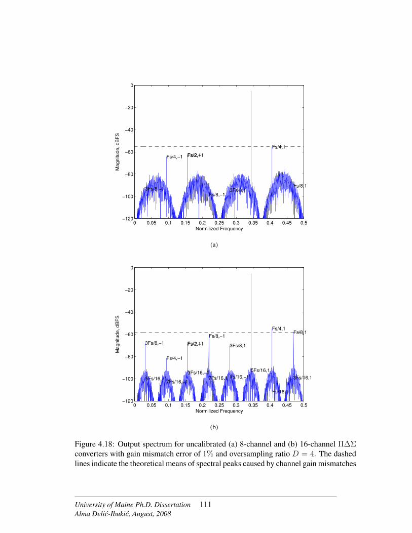
0 0.05 0.1 0.15 0.2 0.25 0.3 0.35 0.4 0.45 0.5−120
−100
−80
−60
−40
−20
0
Normilized Frequency
Mag
nitu
de, d
BFS
Fs/8,1
Fs/8,−1
Fs/4,1
Fs/4,−1
3Fs/8,13Fs/8,−1
Fs/2,1Fs/2,−1
(a)
0 0.05 0.1 0.15 0.2 0.25 0.3 0.35 0.4 0.45 0.5−120
−100
−80
−60
−40
−20
0
Normilized Frequency
Mag
nitu
de, d
BFS
Fs/16,1
Fs/16,−1
Fs/8,1Fs/8,−1
3Fs/16,13Fs/16,−1
Fs/4,1
Fs/4,−1
5Fs/16,1
5Fs/16,−1
3Fs/8,13Fs/8,−1
7Fs/16,17Fs/16,−1
Fs/2,1Fs/2,−1
(b)
Figure 4.18: Output spectrum for uncalibrated (a) 8-channel and (b) 16-channel Π∆Σconverters with gain mismatch error of 1% and oversampling ratio D = 4. The dashedlines indicate the theoretical means of spectral peaks caused by channel gain mismatches
University of Maine Ph.D. DissertationAlma Delic-Ibukic, August, 2008
111

respectively. Also plotted are the theoretical means of spectral peaks that remained after
calibration and are based on the value of Q[n] at the last collected training sample n. As
predicted by theory, the error tones were reduced by 20 dB for Q[n]dB = −60 dB and
by 40 dB for Q[n]dB = −80 dB.
4.10 Calibration Based on Multi-Tone Input Signal
Up until now, the performance of the gain correction algorithm was based on the
input signal samples x[n] having normal distribution with variance σ2x. This ensured that
each channel in an M -channel Π∆Σ converter was processing part of the input signal.
The RLS algorithm cannot detect a gain error for an inactive channel(s), therefore the
input signal must excite all of the channels in the Π∆Σ architecture. If the input signal
constraint is met, the proposed calibration will simultaneously correct for all the chan-
nel gain errors. In software radio (SWR) receiver architectures an ADC is required to
capture an entire cellular band that may contain multiple wireless standards and signals
from different wireless users. This multi-tone input signal can be enough to excite allM
channels of the Π∆Σ architecture, leading to successful gain calibration. An example of
a multi-tone input signal that leads to successful channel gain error correction is given
next.
A 16-channel Π∆Σ converter with an additional channel for calibration was
modelled in MATLAB. Each channel contains a 2nd order ∆Σ modulator with the over-
sampling ratio D = 4. Calibration is demonstrated for a 5 tone input signal. This input
signal shows the wide bandwidth capabilities of Π∆Σ converters and also excites all of
the 16 channels. To have a calibration channel as a linear combination of other channels,
terms αr for r = 1, 2, ..., 16 were set to ±0.25 as identified by computer search. Gain
error mismatches of 1% were simulated and introduced to all channels (including the
calibration channel). Gain correction terms were calculated using the RLS algorithm
described in Table 4.1. Figure 4.21 shows the simulation results for an uncalibrated and
University of Maine Ph.D. DissertationAlma Delic-Ibukic, August, 2008
112

0 0.05 0.1 0.15 0.2 0.25 0.3 0.35 0.4 0.45 0.5−120
−100
−80
−60
−40
−20
0
Normilized frequency
Mag
nitu
de, d
BFS
Fs/8,1
Fs/8,−1
Fs/4,1Fs/4,−1
3Fs/8,13Fs/8,−1Fs/2,1Fs/2,−1
(a)
0 0.05 0.1 0.15 0.2 0.25 0.3 0.35 0.4 0.45 0.5−120
−100
−80
−60
−40
−20
0
Normilized frequency
Mag
nitu
de, d
BFS
Fs/8,1Fs/8,−1
Fs/4,1Fs/4,−1
3Fs/8,13Fs/8,−1
Fs/2,1Fs/2,−1
(b)
Figure 4.19: Performance of an 8-channel Π∆Σ converter after calibration. Gain cor-rection terms were calculated using an RLS algorithm and input signal with zero meanand variance σ2
x. The RLS algorithm was trained to obtain the dynamic range improve-ment of: (a) 20 dB and (b) 40 dB.The dashed lines correspond to theoretical means ofspectral peaks that remained after calibration.
University of Maine Ph.D. DissertationAlma Delic-Ibukic, August, 2008
113

0 0.05 0.1 0.15 0.2 0.25 0.3 0.35 0.4 0.45 0.5−120
−100
−80
−60
−40
−20
0
Normilized frequency
Mag
nitu
de, d
BFS
Fs/16,1Fs/16,−1
Fs/8,1
Fs/8,−1
3Fs/16,1
3Fs/16,−1
Fs/4,1
Fs/4,−1
5Fs/16,1
5Fs/16,−13Fs/8,13Fs/8,−1 7Fs/16,1
7Fs/16,−1
Fs/2,1Fs/2,−1
(a)
0 0.05 0.1 0.15 0.2 0.25 0.3 0.35 0.4 0.45 0.5−120
−100
−80
−60
−40
−20
0
Normilized frequency
Mag
nitu
de, d
BFS
Fs/16,1
Fs/16,−1 Fs/8,1Fs/8,−13Fs/16,1
3Fs/16,−1 Fs/4,1Fs/4,−15Fs/16,1
5Fs/16,−1 3Fs/8,1
3Fs/8,−1
7Fs/16,17Fs/16,−1
Fs/2,1Fs/2,−1
(b)
Figure 4.20: Performance of a 16-channel Π∆Σ converter after calibration. Gain cor-rection terms were calculated using an RLS algorithm and input signal with zero meanand variance σ2
x. The RLS algorithm was trained to obtain the dynamic range improve-ment of: (a) 20 dB and (b) 40 dB. The dashed lines correspond to theoretical means ofspectral peaks that remained after calibration.
University of Maine Ph.D. DissertationAlma Delic-Ibukic, August, 2008
114

a calibrated system. The RLS algorithm successfully converged for a 5 tone input signal
and the unwanted tones are completely removed from the frequency spectrum.
Based on the analysis and findings in Section 4.7, when the signal power at the
output of each channel of the Π∆Σ converter before demodulation is not equal, the
metric Q[n] can be rewritten from (4.63) to
Q[n] =2σ2
v
n
M∑r=1
1
σ2wr
+ σ4v
M∑r=1
1
σ4wr
(4.80)
Term σ2wr is the signal power at the output of the rth channel of Π∆Σ converter be-
fore demodulation. Based on (4.80), the convergence of the RLS algorithm will be
limited by the channel with the minimum signal power. The minimum signal to noise
ratio σ2w/σ
2v for a 5 tone input signal was measured to be 37 dB. The RLS algorithm
will stop converging when Q[n]dB reaches -74 dB or, because the signal power in each
channel is different, a more accurate result is 20 log10
(σ2v
M∑r=1
1
σ2wr
)= −75 dB. Fig-
ure 4.22 shows the RLS algorithm convergence results for the multi-tone input signal
with frequency spectrum shown in Figure 4.21. As expected, the RLS algorithm stops
converging once Q[n]dB reaches -75 dB. Also, the RLS algorithm takes fewer iterations
to saturate because some channels have larger signal to noise ratio σ2w/σ
2v and therefore
converge to the correct solution faster.
University of Maine Ph.D. DissertationAlma Delic-Ibukic, August, 2008
115

0 0.05 0.1 0.15 0.2 0.25 0.3 0.35 0.4 0.45 0.5−140
−120
−100
−80
−60
−40
−20
0
Normilized Frequency
Mag
nitu
de, d
BFS
(a)
0 0.05 0.1 0.15 0.2 0.25 0.3 0.35 0.4 0.45 0.5−140
−120
−100
−80
−60
−40
−20
0
Normilized Frequency
Mag
nitu
de, d
BFS
(b)
Figure 4.21: Simulation results for a 5-tone input: (a) Uncalibrated 16-channel Π∆Σconverter with 1% gain mismatch error and oversampling ratio D = 4 and (b) Perfor-mance of a 16-channel Π∆Σ converter after calibration. Coefficients αr are identical.Frequencies are normalized by the decimated sample rate.
University of Maine Ph.D. DissertationAlma Delic-Ibukic, August, 2008
116
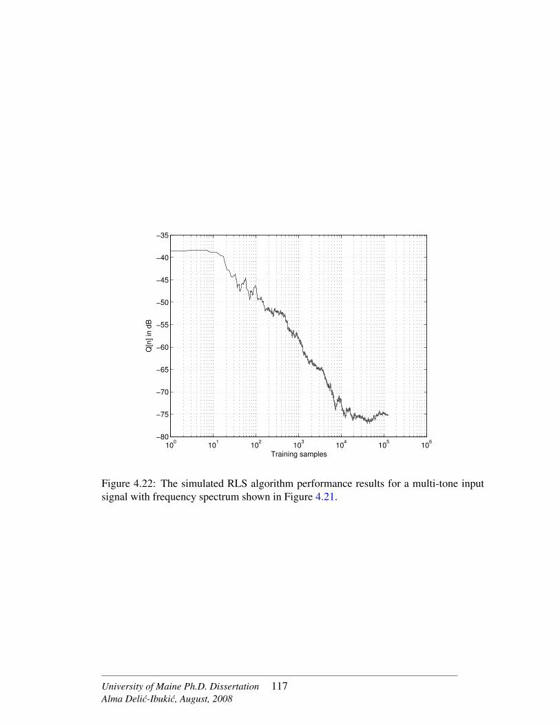
100 101 102 103 104 105 106−80
−75
−70
−65
−60
−55
−50
−45
−40
−35
Training samples
Q[n
] in
dB
Figure 4.22: The simulated RLS algorithm performance results for a multi-tone inputsignal with frequency spectrum shown in Figure 4.21.
University of Maine Ph.D. DissertationAlma Delic-Ibukic, August, 2008
117
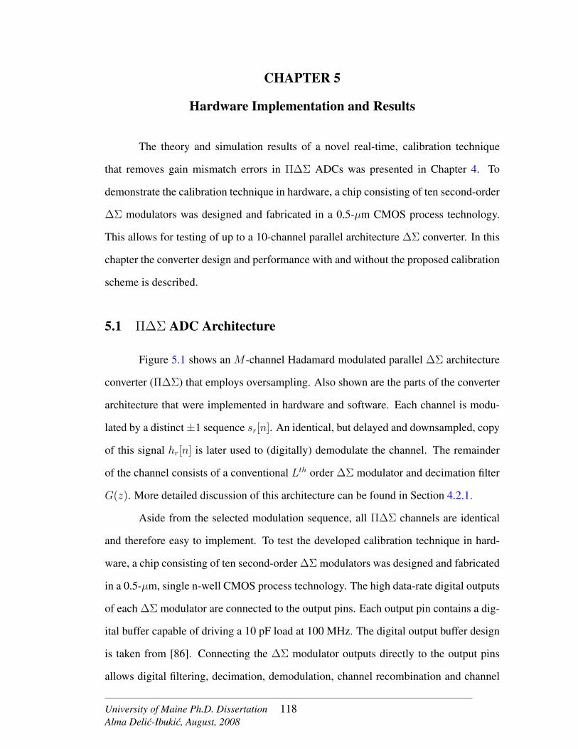
CHAPTER 5
Hardware Implementation and Results
The theory and simulation results of a novel real-time, calibration technique
that removes gain mismatch errors in Π∆Σ ADCs was presented in Chapter 4. To
demonstrate the calibration technique in hardware, a chip consisting of ten second-order
∆Σ modulators was designed and fabricated in a 0.5-µm CMOS process technology.
This allows for testing of up to a 10-channel parallel architecture ∆Σ converter. In this
chapter the converter design and performance with and without the proposed calibration
scheme is described.
5.1 Π∆Σ ADC Architecture
Figure 5.1 shows an M -channel Hadamard modulated parallel ∆Σ architecture
converter (Π∆Σ) that employs oversampling. Also shown are the parts of the converter
architecture that were implemented in hardware and software. Each channel is modu-
lated by a distinct±1 sequence sr[n]. An identical, but delayed and downsampled, copy
of this signal hr[n] is later used to (digitally) demodulate the channel. The remainder
of the channel consists of a conventional Lth order ∆Σ modulator and decimation filter
G(z). More detailed discussion of this architecture can be found in Section 4.2.1.
Aside from the selected modulation sequence, all Π∆Σ channels are identical
and therefore easy to implement. To test the developed calibration technique in hard-
ware, a chip consisting of ten second-order ∆Σ modulators was designed and fabricated
in a 0.5-µm, single n-well CMOS process technology. The high data-rate digital outputs
of each ∆Σ modulator are connected to the output pins. Each output pin contains a dig-
ital buffer capable of driving a 10 pF load at 100 MHz. The digital output buffer design
is taken from [86]. Connecting the ∆Σ modulator outputs directly to the output pins
allows digital filtering, decimation, demodulation, channel recombination and channel
University of Maine Ph.D. DissertationAlma Delic-Ibukic, August, 2008
118

c
c
G(z)
G(z)
G(z)
G(z)
G(z)
G(z)
D
D
D
D
D
D
M−1
c
1
2
3
M−1
M
c
c
c
c
c
M
AlgorithmRLS
M
3
1
s [n]
s [n]
s [n]
s [n]
3h [n]
2h [n]
1h [n]
h [n]
M−1
x[n]
s [n]
s [n]
h [n]
∆Σ
∆Σ
∆Σ
∆Σ
∆Σ
∆Σ
2
y[n]
Implemented on chip Implemented in software
Figure 5.1: Oversampling Π∆Σ ADC with gain calibration. Also shown are the partsof the architecture that were implemented in hardware and software.
University of Maine Ph.D. DissertationAlma Delic-Ibukic, August, 2008
119

gain mismatch calibration to be performed in software.
The second-order ∆Σ modulators are implemented using switched-capacitor
(SC) circuits. A fully differential configuration ensures good power supply noise re-
jection, increased dynamic range, and reduced clock feedthrough [47, 79, 87]. Figure
5.2 shows the fully differential second-order ∆Σ modulator implementation. The topol-
ogy contains two delaying integrators in the forward path and is based on the design
first introduced in [79]. The two integrators consist of an operational transconductance
amplifier (OTA), two sampling capacitors with value C and two integrating capacitors
with value 2C. The linear model of this architecture was introduced in Section 4.2.2,
where gains for the first and second integrator were set to 0.5 and 2, respectively. With
these gains, the ∆Σ modulator output is given as the sum of the delayed input signal
and filtered quantization noise. In Figure 5.2, both integrators are designed to have a
gain of 0.5. This change does not affect the output of ∆Σ modulator because the second
integrator is followed by a 1-bit quantizer and its final decision will be unaffected by
this gain reduction [63, 79].
To operate correctly, the ∆Σ modulators rely on a two-phase, non-overlapping
clock signals, φ1 and φ2. To minimize the charge injection that is inherent in switched
capacitor circuits, a bottom-plate sample-and-hold (S/H) design is used [47, 87]. The
bottom-plate S/H circuit requires extra clock signals to be introduced (φ′1 and φ′2) that
turn off slightly before φ1 and φ2. Since the switches that are controlled by φ′1 and φ′2
are connected to a fixed potential or a virtual ground node, the charge injected by these
switch transitions is independent of the input signal. This constant offset term is further
removed by implementation of a fully differential circuits [47,79]. Figure 5.3 illustrates
the timing waveforms for four clock signals used in the design.
In Figure 5.2, each integrator samples the input signal during φ1. During φ2,
the output of the second integrator is processed by a 1-bit quantizer followed by a 1-
bit D/A converter. The difference between the D/A converter output and the input into
University of Maine Ph.D. DissertationAlma Delic-Ibukic, August, 2008
120
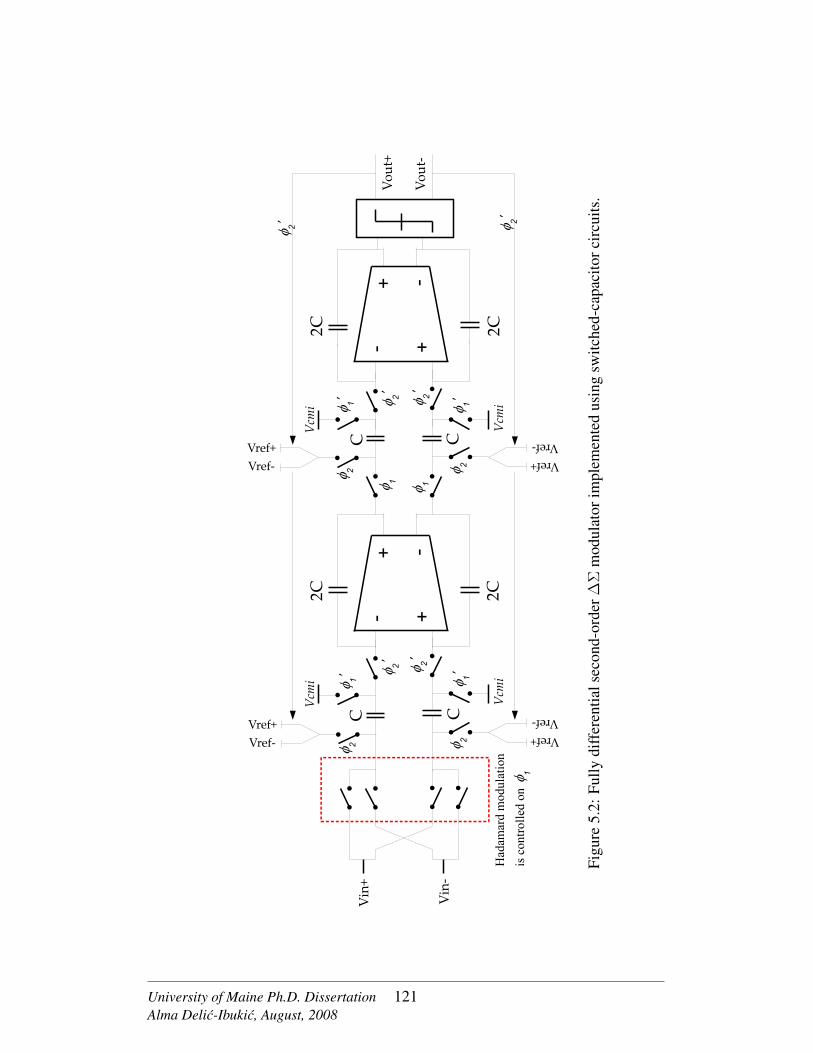
Figu
re5.
2:Fu
llydi
ffer
entia
lsec
ond-
orde
r∆Σ
mod
ulat
orim
plem
ente
dus
ing
switc
hed-
capa
cito
rcir
cuits
.
University of Maine Ph.D. DissertationAlma Delic-Ibukic, August, 2008
121

Figure 5.3: Two-phase, non-overlapping clock timing diagram.
each integrator is transferred to the capacitor labelled 2C. This is the “subtraction and
integration phase”. Because sampling and integration occur at two different clock phases
(i.e. φ1 and φ2), each action should be complete within half the period of the main clock.
If the main clock is running at 50 MHz, each component in ∆Σ modulator circuit must
settle to its final value in 10 ns.
During φ2, the Hadamard modulation sequence is captured and during φ1 based
on the captured sequence switches are configured to pass the differential signal or cross
the inputs to pass the inverse of the differential signal to the stage 1 input. The logic
circuit that performs Hadamard modulation and sizing of all the switches used in Figure
5.2 can be found in the Appendix A.
The fabricated chip operates from a single 5 V supply. To maximize the output
swing, the common-mode voltage was set to 2.5 V. Each ∆Σ modulator accepts a ±1 V
fully differential input signal that is centered around the common-mode voltage. The
two reference voltages VREF+ and VREF− that are required for the ∆Σ modulator op-
eration are set to 3 V and 2 V, respectively. This corresponds to a 1-bit D/A output of
±1 V. The 1-bit D/A output is controlled by a 1-bit quantizer at the output of the second
integrator. In Figure 5.2, the nodes labelled V cmi set the common mode input voltage
of the differential OTA input. In this design, V cmi was set to 1.5 V. All the required
University of Maine Ph.D. DissertationAlma Delic-Ibukic, August, 2008
122

Figure 5.4: Die microphotograph. Die measures 3704 µm by 2620 µm; it contains ten2nd order ∆Σ modulators and two-phase, non-overlapping clock generator.
common-mode and reference voltages are supplied off-chip.
Figure 5.4 shows a die microphotograph that contains ten second-order ∆Σ mod-
ulators and a two-phase, non-overlapping clock generator. The die also contains cir-
cuitry required to preform Hadamard modulation at the input of each ∆Σ modulator.
The die measures 3704 µm by 2620 µm and is packaged in a 40-pin DIP. The following
section gives an overview of a ∆Σ modulator building blocks and circuit techniques
used to implement them.
5.2 Design Overview
When designing switched-capacitor ∆Σ A/D converters, important considera-
tion is given to the DC gain of the OTA, the input-referred thermal noise (i.e. sampling
noise) and the OTA current required to drive capacitive loads quickly and accurately (i.e.
slew-rate limit) [13,63,79,88]. This section also gives an overview of a fully differential
University of Maine Ph.D. DissertationAlma Delic-Ibukic, August, 2008
123

Figure 5.5: Implementation of SC integrator.
gain-boosting OTA with common-mode feedback that was adopted for the final design.
5.2.1 OTA DC Gain Requirements
Figure 5.5 shows a switched-capacitor (SC) integrator implemented using two-
phase, non-overlapping clock signals, φ1 and φ2. Parasitic capacitances due to the OTA
are assumed to be negligible. If the OTA is assumed to have finite DC gain A, then
vout = A(v+ − v−) = −Av− (5.1)
where v+ and v− are voltages seen at the positive and negative input terminals of the
OTA, respectively. Based on the timing diagram of clocks φ1 and φ2 in Figure 5.6, the
total charge stored on the integrator in Figure 5.5 at the end of φ1 is given by
q[n− 1] = vin[n− 1]Cs+ vout[n− 1]Ci
(1 + A
A
)(5.2)
The total charge stored on the integrator at the end of φ2 is given by
q[n− 1
2] = vout[n−
1
2]Cs
A+ vout[n−
1
2]Ci
(1 + A
A
)= vout[n]
Cs
A+ vout[n]Ci
(1 + A
A
)(5.3)
University of Maine Ph.D. DissertationAlma Delic-Ibukic, August, 2008
124

Figure 5.6: Two-phase, non-overlapping clock timing diagram indicating sampling in-stances.
The second line of (5.3) holds since during φ1, the voltage across Ci is constant, result-
ing in vout[n − 12] = vout[n]. In order to maintain charge conservation in the circuit,
q[n− 1] = q[n− 12]. By equating (5.2) and (5.3), the relationship between the integrator
input vin and output vout can be found.
vin[n− 1]Cs = vout[n]
(Cs
A+ Ci
(1 + A
A
))− vout[n]Ci
(1 + A
A
)(5.4)
The z-domain transfer function of the SC integrator with a finite DC gain of A is given
by
Vout(z)
Vin(z)=
ACsz−1
Cs+ (1 + A)Ci(1− z−1)
=Cs
Ci
(1
1 + 1A
+ CsCiA
)(z−1
1− z−1 Ci(A+1)Ci(A+1)+Cs
)
=Cs
Ci
(1
1 + 1A
+ CsCiA
)(z−1
1− z−1(1− CsCiA+Ci+Cs
)
)
' Cs
Ci
(1
1 + 1A
+ CsCiA
)(z−1
1− z−1(1− CsCiA
)
)(5.5)
University of Maine Ph.D. DissertationAlma Delic-Ibukic, August, 2008
125

Equation (5.5) shows that if a DC gain of the OTA is not large enough, there will be a
pole introduced by the integrator. This is known as integrator leakage because only (1−CsCiA
) of the integrator’s previous output will be added to every new input sample [63,79].
Integrator leakage will reduce the noise suppression at low frequencies, which in turn
degrades the final resolution of ∆Σ modulators.
To ensure large DC gain, a fully differential telescopic OTA with gain boosting
is implemented. The OTA design overview is given later in the chapter.
5.2.2 kT/C Noise and Capacitor Sizing
In order to properly size capacitors required to implement a second-order ∆Σ
modulator in Figure 5.2, the input-referred thermal noise of the first integrator is con-
sidered. Here, it is assumed that all of the input-referred thermal noise is contributed by
the switches that charge/discharge the sampling capacitor C. Because the circuit is fully
differential and the noise power adds up, the input-referred thermal noise power due to
switches is given by
σ2tn = 2× 2kT
D · C(5.6)
where k is Boltzmann’s constant, T is the absolute temperature and D is the oversam-
pling rate [13]. From (5.6) it can be seen that increasing the oversampling rate and
sampling capacitor C of the first integrator will reduce the input-referred noise power.
The design goal was to achieve an 11-bit converter performance with an oversampling
rate D = 2. For a second-order ∆Σ modulator, the signal-to-noise ratio (SNR) is given
by [13, 89]
SNRdB = 10 log10
(σ2s
σ2e
)= n · 6.02 + 1.76 + 50 log10(D)− 10 log10
(π4
5
)(5.7)
University of Maine Ph.D. DissertationAlma Delic-Ibukic, August, 2008
126
where σ2s is the maximum input signal power, σ2
e is the quantization noise power de-
scribed in Section 2.4.2, n is the desired number of bits and D is the oversampling rate.
Based on (5.7), the maximum SNR for an 11-bit ∆Σ ADC with D = 2 is 70 dB. The
input-referred thermal noise σ2tn was chosen to be 4 dB lower than the maximum SNR
for an 11-bit ∆Σ ADC. Also, the design accepts ±1-V differential input signal and
therefore the maximum mean square voltage σ2s for a sinusoidal input is 0.5-V2. With
these restrictions, σ2tn for SNR of 74 dB and input variance of 0.5-V2 is found to be
σ2tn =
0.5
107.4= 20 · 10−9 V2 (5.8)
By using (5.6), D = 2 and the result of (5.8), the lower limit on the required sampling
capacitor C was found to be 414-fF. The sampling capacitor C in Figure 5.2 was chosen
to be 500-fF, which in turn requires an integrating capacitor 2C of 1-pF.
5.2.3 OTA Slew Rate Requirements
Referring to Figure 5.2, during φ2, integrators of a second-order ∆Σ modulator
directly sample the output of a 1-bit DAC causing the OTA to see large signal at its
input terminals. Because the output of the OTA cannot change instantaneously, the
OTA is driven out of its linear region of operation and is expected to slew for most of
φ2 [88, 90]. The slew rate (SR) is given by
SR =I
Ce(5.9)
where I is the maximum bias current available at the OTA output node for charg-
ing/discharging of the external capacitance Ce. As mentioned in Section 5.1, sampling
and integration occur during two different clock phases, therefore each action needs to
be completed within half the period of the main clock. The design goal is to minimize
the slew rate, and therefore minimize the current required for the OTA to complete the
University of Maine Ph.D. DissertationAlma Delic-Ibukic, August, 2008
127

Figure 5.7: SC integrator configuration used to determine the effective capacitance Cewhen φ2 is high. Feedback is not effective because the OTA will be slewing for most ofφ2.
integration and ensure the output settles to a final value (within some allowable error
range) by the end of φ2.
For the given converter design, a full-scale analog input range is 2 V (i.e. ±1 V
differential). Based on the ∆Σ modulator topology used and results found in [79], to
support input signals that are 1 dB below full-scale, the output of both integrators should
be at least 50 % larger than the full-scale analog input range. This means that for a full-
scale analog input range of 2 V, the output swing of the OTA should be 3 V. If the main
clock is running at 50 MHz, integration needs to complete within 10 ns. Therefore, to
avoid distortion from slewing, the minimum OTA slew rate is 300 V/µs.
In order to find the OTA current that meets the minimum slew rate requirements,
the capacitance Ce seen at the output node of the OTA to ground during φ2 must be
estimated. Figure 5.7 shows the SC integrator configuration when the clock signal φ2
is high. As mentioned before, the OTA will be slewing for most of φ2. During the
slewing period, the operation of the OTA is nonlinear and therefore the feedback is not
effective [88,90]. The total capacitanceCe seen at the output node of the OTA to ground
during φ2 is given by
Ce = Cl +CiCs
Ci+ Cs(5.10)
University of Maine Ph.D. DissertationAlma Delic-Ibukic, August, 2008
128

Assuming the load capacitance Cl is the same size as the sampling capacitor Cs and
using capacitor values found in Section 5.2.2, the total capacitance Ce seen at the output
node of the OTA during φ2 is approximately 1 pF. Knowing the minimum slew rate
requirement, (5.9) can be used to find the minimum current I required to drive the
external capacitance Ce. For this design, the minimum current requirement is 300 µA.
This is the current required at a single output node of the OTA. For the differential
implementation, the total OTA bias current ISS should be at least 600 µA to provide the
required capability to charge both of the differential branches.
5.2.4 Fully Differential Gain Boosting OTA
In order to achieve high DC gain, the telescopic OTA architecture with gain
boosting was implemented [91–94]. Figure 5.8 shows a fully differential implementa-
tion of a telescopic OTA with gain boosting and common-mode feedback (CMFB). Also
shown are device sizings used in the final design. Circuits that generate biasing voltages
V b1 and V b2 can be found in Appendix A. The gain-boosting techniques increase the
output resistance of the telescopic OTA without the need for additional cascode stages.
Negative feedback is used to maintain a relatively constant output current by reducing
the drain voltage variations for M1, M2, M7 and M8. Minimizing current variations
(i.e. current remains more constant) translates into an increase in the output resistance
of the OTA.
Because the circuit implementation is fully differential (i.e. left and right side
are identical in implementation), it is sufficient to analyze only one side. The overall
voltage gain for a gain-boosting OTA in Figure 5.8 is given by [90]
Av ∼= gm7 · (ro7ro5gm5(1 + Agbn)) ‖ (ro1ro3gm3(1 + Agbp)) (5.11)
where gm and ro terms are small signal device transconductance and output resistance,
University of Maine Ph.D. DissertationAlma Delic-Ibukic, August, 2008
129

M1 60µm/0.6µm M2 60µm/0.6µm M3 60µm/0.6µm M4 60µm/0.6µmM5 120µm/0.6µm M6 120µm/0.6µm M7 400µm/0.6µm M8 400µm/0.6µmM9 240µm/1.5µm M10 60µm/1.5µm
Figure 5.8: Fully differential telescopic OTA with gain boosting and common-modefeedback (CMFB).
University of Maine Ph.D. DissertationAlma Delic-Ibukic, August, 2008
130

(a) Differential GB amplifier for an NMOS cascodepair in Figure 5.8.
M1 24µm/0.6µm M2 24µm/0.6µm M3 12µm/1.5µmM4 12µm/1.5µm M5 300µm/1.5µm
(b) Differential GB amplifier for a PMOS cascode pairin Figure 5.8.
M1 60µm/1.5µm M2 60µm/1.5µm M3 72µm/0.6µmM4 72µm/0.6µm M5 120µm/0.6µm
Figure 5.9: Differential gain boosting amplifiers used in the design of the OTA in Figure5.8.
University of Maine Ph.D. DissertationAlma Delic-Ibukic, August, 2008
131

respectively. Terms labelled Agbn and Agbp are DC gains of auxiliary amplifiers that
provide gain boosting to the NMOS and PMOS cascode pairs, respectively. In this
design, a common-source amplifiers were used for gain-boosting. Their fully differential
implementation is shown in Figure 5.9. Also included in the figure are the device sizes
used in the design. Circuits that generate biasing voltages V b3 and V b4 can be found
in Appendix A. For this design, the DC gain of the auxiliary amplifiers is given by
Agbn = gm3(ro3 ‖ ro1) and Agbp = gm3(ro1 ‖ ro3) based on Figures 5.9(a) and 5.9(b),
respectively.
A drawback of fully differential amplifier is the requirement of a common-mode
feedback (CMFB) circuit in order to operate properly. Fully differential amplifiers
don’t have a well defined common-mode (CM) level at the output nodes. If the out-
put nodes are not kept fixed at some DC level, they will drift, causing the amplifier
to saturate. The purpose of the CMFB circuit is to sense the output CM level (i.e.
Vout,cm = (Vout++Vout−)2
), compare it with the reference voltage VCM , and adjust the am-
plifier’s bias circuitry to maintain a specific output CM level [87, 90]. The output CM
levels are kept around the reference voltage VCM .
Figure 5.10 shows the CMFB circuit that controls the output CM level by current
steering. Also shown are device sizes used in the design. The design was adapted from
[90] and modified to meet the design requirements. The circuit senses the difference
between Vout,cm and VCM and produces a current through M5 that is proportional to this
difference. Also, transistorM5 will contain a DC current term that is equal to the CMFB
circuit bias current generated by V b1 and transistors M6 and M7. The total current is
mirrored to the OTA by transistor M10 in Figure 5.8. Transistor M10 together with M9
forms the tail current of the OTA which controls the output CM levels.
Open loop frequency response and slew rate limit tests were conducted to char-
acterize the final design of the fully differential OTA with gain-boosting and CMFB.
Two open loop frequency response characteristics of interest are phase margin and unity
University of Maine Ph.D. DissertationAlma Delic-Ibukic, August, 2008
132

M1 7.5µm/0.6µm M2 7.5µm/0.6µm M3 7.5µm/0.6µm M4 7.5µm/0.6µmM5 60µm/1.5µm M6 36µm/0.6µm M7 36µm/0.6µm M8 60µm/1.5µm
Figure 5.10: Common mode feedback circuit used in the design of a gain boosting OTA.
0.5 1 1.5 2 2.5 3 3.5 40
10
20
30
40
50
60
70
Pha
se M
argi
n (d
egre
es)
CL (pF)
0.5 1 1.5 2 2.5 3 3.5 4108
109
1010
Uni
ty g
ain
frequ
ency
(Hz)
Figure 5.11: Open loop frequency response (phase margin and unity gain frequency) fordifferent load capacitances CL. Star symbol corresponds to unity gain frequency axisand asterisk symbol correspond to phase margin axes.
University of Maine Ph.D. DissertationAlma Delic-Ibukic, August, 2008
133

Figure 5.12: Circuit setup to test the open loop frequency response of the OTA.
gain frequency. For the given OTA design topology, the overall transfer function will
have a dominant pole due to a capacitive load CL located at the output node of the OTA.
However, the given topology also has a pole-zero doublet present in its transfer function
which is a side-effect of gain-boosting [92,95]. The existence of a pole-zero doublet can
have a negative affect on the phase margin and/or the settling time of the OTA. Circuit
configurations to run the open loop frequency response and slew rate tests were adapted
from [96] and are shown in Figures 5.12 and 5.13, respectively.
Figure 5.11 shows the simulated open loop frequency response behavior of the
OTA as a function of load capacitances CL. The OTA was simulated with the common-
mode input voltage V cmi set to 1.5 V and the common-mode output voltage VCM set
to 2.5 V. Figure 5.11 shows reduced phase margin due to a pole-zero doublet and low
values of CL. As CL increases, separation between the dominant pole and pole-zero
doublet increases causing a more stable frequency response with a reduced unity gain
frequency. A summary of a fully differential gain-boosting OTA with CMFB is given in
Table 5.1.
University of Maine Ph.D. DissertationAlma Delic-Ibukic, August, 2008
134
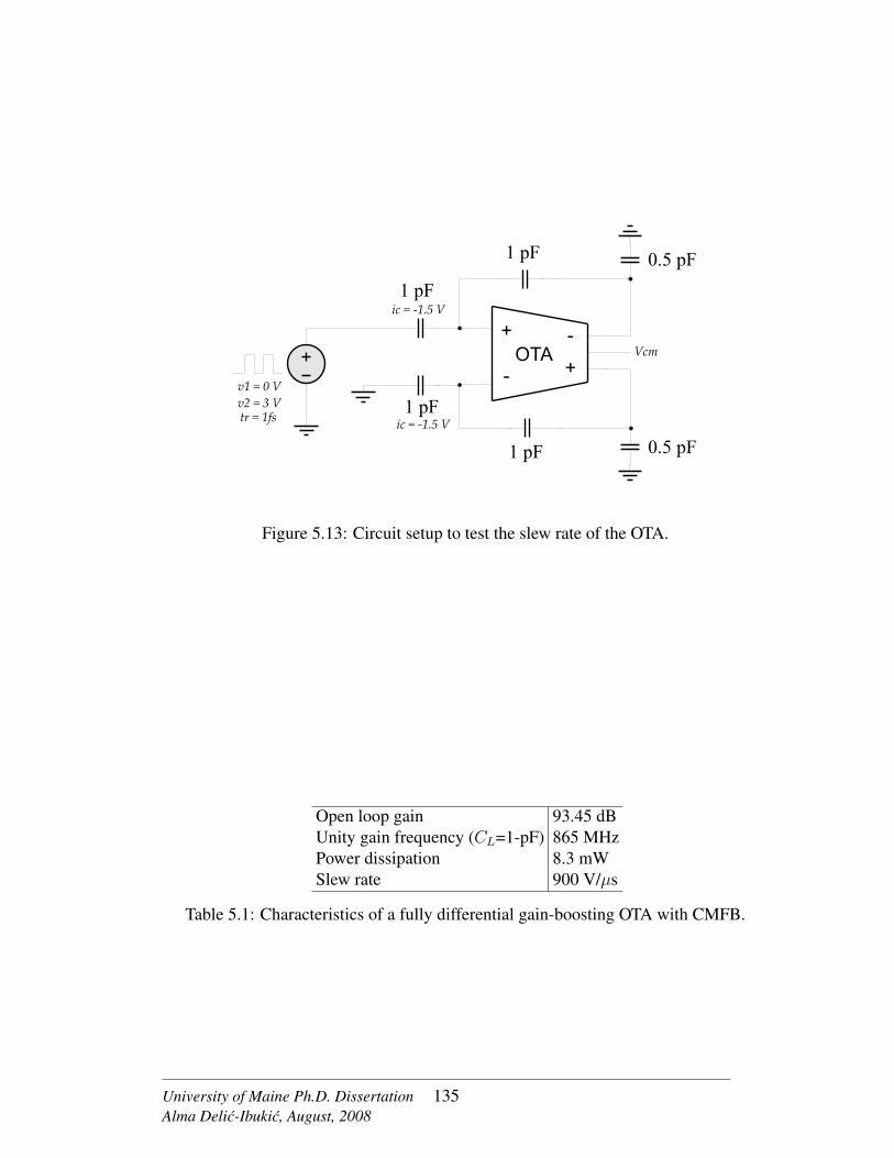
Figure 5.13: Circuit setup to test the slew rate of the OTA.
Open loop gain 93.45 dBUnity gain frequency (CL=1-pF) 865 MHzPower dissipation 8.3 mWSlew rate 900 V/µs
Table 5.1: Characteristics of a fully differential gain-boosting OTA with CMFB.
University of Maine Ph.D. DissertationAlma Delic-Ibukic, August, 2008
135

5.2.5 Remaining ∆Σ Modulator Components
The remaining ∆Σ modulator components are the 1-bit DAC, 1-bit comparator
and the two-phase, non-overlapping clock signal generator. Full schematics and device
sizes for all of these components are provided in Appendix A.
The comparator design was motivated by a design reported in [97] and is shown
in Figure 5.14. It was sized to meet the current design requirements and its performance
at 50 MHz can be found in [86]. From Figure 5.14, transistors M1-M6 are the input
stage of the comparator and are always active. When Latch is high, transistors M11
and M12 pull the gates of M7-M10 low making them inactive and M12 and M14
make sure that the output nodes are pulled high. Therefore, during the comparator’s off-
time, the output nodes are always pulled high, which makes sure that a decision from a
previous comparison is always erased. When Latch is low, M15 is active which in turn
deactivates M13, M14 and M16. During this time the comparator makes the decision
and depending on the applied input, the positive feedback formed by M9 and M10 will
pull one of the output nodes low.
Both the comparator decision and its compliment are provided at the output
nodes. However, the modulator design does not directly utilize the compliment. In-
stead, the compliment is obtained by directly inverting the comparator decision. The
inverter is part of the 1-bit D/A converter design logic. This was done to avoid indeci-
sive comparator outputs [86].
The 1-bit D/A converter design and device sizes are provided in Appendix A.
The D/A converter uses two minimum sized inverters and four NMOS switches that
are controlled by the comparator output. Depending on the comparator decision, the
1-bit D/A converter will produce ±1 V differential output. This is based on VREF+
and VREF− being 3 V and 2 V, respectively. The two-phase, non-overlapping clock
generator was based on the design in [47, 86], and it was modified to meet current de-
sign requirements. The design and device sizes for the clock generator are provided in
University of Maine Ph.D. DissertationAlma Delic-Ibukic, August, 2008
136

Figure 5.14: A two-stage high-speed comparator.
Appendix A.
5.3 Test and Characterization
To test the calibration scheme presented in Chapter 4, a four-layer printed circuit
(PC) board was designed and fabricated. The fabricated board is shown in Figure 5.15.
The PC board supports two custom designed chips with each containing ten second-
order ∆Σ modulators. The two inner layers of the PC board are used as ground and
power planes. The test board requires two separate power supplies, one to drive the two
chips and reference generation circuitry (VDD), and the other to drive digital circuitry
responsible for capturing data from the two chips (VCC). The power plane was connected
to VDD, while VCC was routed to required components using top and bottom layers of
the four-layer board. The test board schematics and PC board layout are provided in
Appendix B.
The PC board can be configured to run either two of the chips independent of
University of Maine Ph.D. DissertationAlma Delic-Ibukic, August, 2008
137
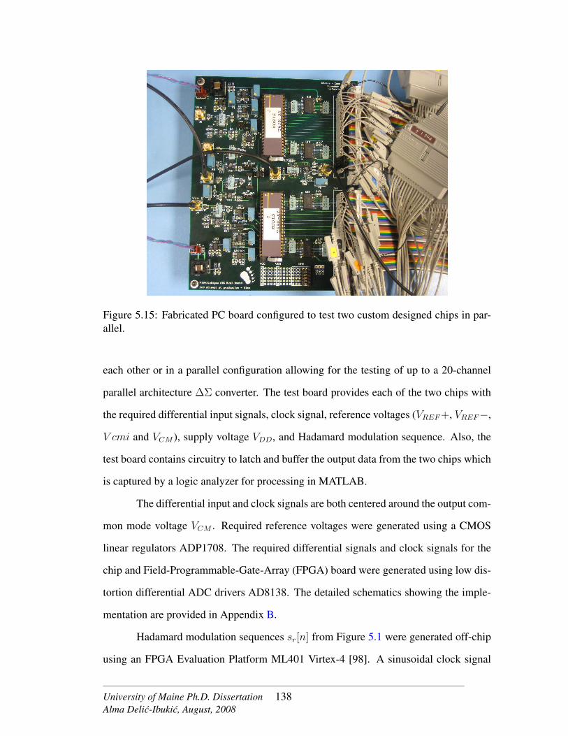
Figure 5.15: Fabricated PC board configured to test two custom designed chips in par-allel.
each other or in a parallel configuration allowing for the testing of up to a 20-channel
parallel architecture ∆Σ converter. The test board provides each of the two chips with
the required differential input signals, clock signal, reference voltages (VREF+, VREF−,
V cmi and VCM ), supply voltage VDD, and Hadamard modulation sequence. Also, the
test board contains circuitry to latch and buffer the output data from the two chips which
is captured by a logic analyzer for processing in MATLAB.
The differential input and clock signals are both centered around the output com-
mon mode voltage VCM . Required reference voltages were generated using a CMOS
linear regulators ADP1708. The required differential signals and clock signals for the
chip and Field-Programmable-Gate-Array (FPGA) board were generated using low dis-
tortion differential ADC drivers AD8138. The detailed schematics showing the imple-
mentation are provided in Appendix B.
Hadamard modulation sequences sr[n] from Figure 5.1 were generated off-chip
using an FPGA Evaluation Platform ML401 Virtex-4 [98]. A sinusoidal clock signal
University of Maine Ph.D. DissertationAlma Delic-Ibukic, August, 2008
138

Device Model FunctionSignal Generator HP8645A Input signalSignal Generator HP8642A ClockSystem DC Power Supply HP6621A V DD and V CC supply for
the chipLogic Analyzer Agilent 16823A Used to capture dataFPGA Evaluation Platform ML401 Virtex-4 Used to generate Hadamard
modulation sequence
Table 5.2: Equipment used to test custom designed chip that contains ten second-order∆Σ modualtors.
generated by an HP8642 was passed through a splitter with one signal routed to generate
the required clock signal for the chip and the other signal routed to generate the clock for
the FPGA board. Table 5.2 lists the equipment used to test the Π∆Σ ADC and collect
data.
Once the high-data rate digital outputs from the two chips are collected, digital
filtering, decimation, demodulation, channel recombination and calibration were per-
formed in MATLAB. The following sections discuss the performance of the ∆Σ test
chip with and without calibration.
5.4 Performance Test
The power consumption of a single chip that contains 10 second-order ∆Σ mod-
ulators was measured at 175-mW. Performance of an 8-channel and 16-channel Π∆Σ
converter with Nyquist-rate frequency FS = 1.25 MHz and oversampling ratio D = 4
was examined. To calibrate both setups, an Agilent 33120A arbitrary waveform genera-
tor was used to generate a Gaussian noise input. In all cases, input noise and sinusoidal
test signals were filtered before being applied as ADC inputs. The lowpass filter cutoff
frequency was fixed at 2.5 MHz.
University of Maine Ph.D. DissertationAlma Delic-Ibukic, August, 2008
139

5.4.1 Real-Time Calibration Results for an 8-channel Π∆Σ ADC
The ADC test board was configured to run nine ∆Σ modulators in a parallel
configuration. This creates an 8-channel Π∆Σ converter plus an additional channel
used for calibration of channel gain mismatches.
Figure 5.16 shows the real-time data output spectrum for the uncalibrated 8-
channel Π∆Σ converter for two different input frequencies (350 kHz and 430 kHz). In
both cases, the amplitude of the input signal was set at -6 dB of full scale. Using an
Agilent logic analyzer, a sequence of 219 binary output samples per ∆Σ modulator was
collected. The collected data was filtered, downsampled and demodulated in software
to obtain 8192 samples. The output spectrum calculated from these samples is shown
in Figure 5.16. The output spectrum shows spurs due to channel gain mismatches and
harmonic distortion. The harmonic distortion terms are caused by the signal genera-
tor. Harmonics below 2.5 MHz are passed through the lowpass filter to the ADC input.
These additional tones alias back into the signal band (FS/2), and are labelled by a
single integer indicating the harmonic number. Distortion caused by channel gain mis-
matches is expected to appear at frequencies of FSM± Fin, as described in Section 4.3.
These terms are also labelled in the figure. The goal of gain calibration is to reduce these
undesired terms. The dashed line corresponds to a theoretical mean of spectral peaks
caused by channel gain mismatches given by (4.68). By looking at the standard devia-
tion of the estimated coefficients β[n] (after calibration), the channel gain mismatches
for the fabricated chip and given test setup were found to be in the order of 0.5%.
The quantization noise power at the output of each channel σ2v before demodula-
tion is determined by removing the signal component and all the distortion terms from
the output spectrum. The quantization noise power for the 8-channel Π∆Σ converter
experimental setup was found to be 8 · σ2v∼= 8 · 10−6 V2. Quantization noise is expected
to be equally distributed in all 8 channels and therefore the noise seen at the output of
each channel before demodulation σ2v is 10−6 V2.
University of Maine Ph.D. DissertationAlma Delic-Ibukic, August, 2008
140

To test the gain calibration algorithm, the ADC was driven using a Gaussian
input signal with a signal-to-noise ratio of 28 dB. For a signal-to-noise ratio σ2w/σ
2v of
28 dB, the signal power seen at the output of each channel σ2w can be determined. As
before, for an 8-channel converter, the relationship between σ2w and input variance σ2
x is
given by (4.65). The Gaussian noise with variance σ2x was generated using an Agilent
33120A arbitrary waveform generator and a new buffer of ADC output samples was
collected. The RLS algorithm summarized in Table 4.1 was used to determine gain
error correction terms β[n], based on n = 131, 000 independent training samples.
For the 28 dB signal-to-noise ratio, based on the results summarized in Table
4.2, the RLS algorithm will stop converging once Q[n] reaches -56 dB. Based on the
channel gain mismatch error of 0.5% and results in Section 4.9, the dynamic range of
an 8-channel Π∆Σ converter is expected to improve by 10 dB. Also, based on (4.63),
number of training samples n required forQ[n] to reach -56 dB is approximately 10,000.
Training for n = 131, 000 should not improve the performance of the RLS algorithm.
Following the calibration, the derived correction terms β[n] were used to recalculate the
output spectrum. Figure 5.17 shows the real-time data output spectrums for calibrated 8-
channel Π∆Σ converter. The dashed line indicates the expected mean of spectral peaks
after calibration. The experimental results are in the agreement with the theory derived
in Section 4.9. As expected, training for longer than 10,000 samples did not improve
the estimation of gain correction terms.
5.4.2 Real-Time Calibration Results for a 16-channel Π∆Σ ADC
The ADC test board was configured to run seventeen ∆Σ modulators in parallel.
This enables testing of a 16-channel Π∆Σ converter. The extra channel is used for
calibration of channel gain mismatches.
Figure 5.18 shows the real-time data output spectrum for the uncalibrated 16-
channel Π∆Σ converter. As for the 8-channel case, the two single tone test frequencies
University of Maine Ph.D. DissertationAlma Delic-Ibukic, August, 2008
141

0 0.1 0.2 0.3 0.4 0.5 0.6−120
−100
−80
−60
−40
−20
0
Frequency (MHz)
Mag
nitu
de, d
BFS
1
23
4
5
6
7
89
10Fs/8,1Fs/8,−1
Fs/8,2Fs/8,−2Fs/4,1Fs/4,−1 Fs/4,2 Fs/4,−23Fs/8,1
3Fs/8,−13Fs/8,2
3Fs/8,−2
Fs/2,1Fs/2,−1
Fs/2,2Fs/2,−2
(a)
0 0.1 0.2 0.3 0.4 0.5 0.6−120
−100
−80
−60
−40
−20
0
Frequency (MHz)
Mag
nitu
de, d
BFS
1
2
3
4
56
7
8
9
10
Fs/8,1Fs/8,−1Fs/8,2
Fs/8,−2
Fs/4,1Fs/4,−1
Fs/4,2Fs/4,−2
3Fs/8,13Fs/8,−1
3Fs/8,23Fs/8,−2Fs/2,1Fs/2,−1
Fs/2,2Fs/2,−2
(b)
Figure 5.16: Experimental performance of uncalibrated 8-channel Π∆Σ converter with(a) Fin = 350 kHz (b) Fin = 430 kHz. The dashed line corresponds to a theoreticalmean of spectral peaks caused by channel gain mismatches.
University of Maine Ph.D. DissertationAlma Delic-Ibukic, August, 2008
142

0 0.1 0.2 0.3 0.4 0.5 0.6−120
−100
−80
−60
−40
−20
0
Frequency (MHz)
Mag
nitu
de, d
BFS
1
23
4
5
6
7
89
10Fs/8,1Fs/8,−1
Fs/8,2Fs/8,−2
Fs/4,1
Fs/4,−1 Fs/4,2 Fs/4,−23Fs/8,1
3Fs/8,−13Fs/8,2
3Fs/8,−2
Fs/2,1Fs/2,−1
Fs/2,2Fs/2,−2
(a)
0 0.1 0.2 0.3 0.4 0.5 0.6−120
−100
−80
−60
−40
−20
0
Frequency (MHz)
Mag
nitu
de, d
BFS
1
2
3
4
56
7
8
9
10
Fs/8,1Fs/8,−1Fs/8,2
Fs/8,−2Fs/4,1
Fs/4,−1Fs/4,2
Fs/4,−2
3Fs/8,13Fs/8,−1
3Fs/8,23Fs/8,−2
Fs/2,1Fs/2,−1Fs/2,2Fs/2,−2
(b)
Figure 5.17: Experimental performance of an 8-channel Π∆Σ converter after calibra-tion. Calibration results are based on the signal-to-noise ratio σ2
w/σ2v = 28 dB. The
output spectrums for: (a) Fin = 350 kHz (b) Fin = 430 kHz are plotted. The dashedline indicates the expected mean of spectral peaks after calibration.
University of Maine Ph.D. DissertationAlma Delic-Ibukic, August, 2008
143

used are 430 kHz and 350 kHz. The amplitude of the input signal was set to -6 dB of full
scale. Using an Agilent logic analyzer, a sequence of 219 binary output samples per ∆Σ
modulator was collected. This data was filtered, decimated and demodulated in software
to obtain 8192 samples. The output spectrum calculated from these samples is shown
in Figure 5.18. The output spectrum shows terms due to channel gain mismatches and
harmonic distortion. The dashed line corresponds to theoretical mean of spectral peaks
caused by channel gain mismatches given by (4.68). The channel gain mismatches
for the fabricated chip and given test set up are found to be 0.5%. This is based on
the standard deviation of the estimated coefficients β[n] which are directly related to
channel gain errors as shown in Section 4.9.
For calibration, the quantization noise power σ2v seen at the output of each chan-
nel is determined. By removing a signal component and distortion terms from the output
spectrum, the total quantization noise power for a 16-channel Π∆Σ ADC was found to
be 16 · σ2v∼= 9.6 · 10−8 V2. Therefore, the quantization noise variance seen at the output
of each channel before demodulation σ2v is 6 · 10−9 V2. A Gaussian input with 42 dB
signal-to-noise ratio was applied to the converter to test the RLS algorithm. For a signal
to noise ratio σ2w/σ
2v of 42 dB, the signal variance seen at the output of each channel
σ2w can be determined. For the 16-channel converter, the relationship between the input
variance σ2x and σ2
w is given by (4.79). The Gaussian input was generated using an Agi-
lent 33120A arbitrary waveform generator and calibration data was collected. The RLS
algorithm summarized in Table 4.1 was used to determine gain error correction terms
β[n].
Based on the results summarized in Table 4.2, the RLS algorithm will stop con-
verging onceQ[n] reaches -84 dB. Given a signal to noise ratio σ2w/σ
2v and mean-squared
error Q[n], the required number of training samples n can be determined from (4.63).
For this experiment, a signal-to-noise ratio of 42 dB and two different values of Q[n]dB
were used, namely -62 dB and -79 dB. This was based on the RLS algorithm training for
University of Maine Ph.D. DissertationAlma Delic-Ibukic, August, 2008
144

0 0.1 0.2 0.3 0.4 0.5 0.6−120
−100
−80
−60
−40
−20
0
Frequency (MHz)
Mag
nitu
de, d
BFS
1
23
4
5
6
7
8910
Fs/16,1Fs/16,−1
Fs/8,1
Fs/8,−13Fs/16,13Fs/16,−1
Fs/4,1
Fs/4,−1
5Fs/16,1
5Fs/16,−1
3Fs/8,1
3Fs/8,−1
7Fs/16,17Fs/16,−1
Fs/2,1Fs/2,−1
(a)
0 0.1 0.2 0.3 0.4 0.5 0.6−120
−100
−80
−60
−40
−20
0
Frequency (MHz)
Mag
nitu
de, d
BFS
1
2
3
45
67
8
9 10Fs/16,1Fs/16,−1
Fs/8,1
Fs/8,−1 3Fs/16,1
3Fs/16,−1
Fs/4,1
Fs/4,−1
5Fs/16,1
5Fs/16,−1
3Fs/8,1
3Fs/8,−1
7Fs/16,1
7Fs/16,−1
Fs/2,1Fs/2,−1
(b)
Figure 5.18: Output spectrum for uncalibrated 16-channel Π∆Σ converter with (a)Fin = 350kHz and (b) Fin = 430 kHz. The dashed line corresponds to a theoreticalmean of spectral peaks caused by channel gain mismatches.
University of Maine Ph.D. DissertationAlma Delic-Ibukic, August, 2008
145
3000 and 131,000 samples, respectively. Based on the channel gain mismatch error of
0.5% and results in Section 4.9, the dynamic range for a 16-channel Π∆Σ converter is
expected to improve by 16 dB for Q[n] = −62 dB and 33 dB for Q[n] = −79 dB. Fig-
ures 5.19 and 5.20 show the output spectrum for a 16-channel Π∆Σ converter after cal-
ibration for dynamic range improvement of 16 dB and 33 dB, respectively. The dashed
line indicates the expected mean of spectral peaks due to channel gain mismatches after
calibration.
Based on the theory and simulation results in Section 4.9, for a 16-channel Π∆Σ
converter with signal-to-noise ratio of 42 dB and mean-squared error Q[n]dB of -79 dB,
all the gain error terms in a frequency spectrum are expected to not exceed the noise
level of the converter. This is not the case as seen in Figure 5.20, where some of the
distortion terms are above the noise level.
To run this 16-channel Π∆Σ converter experiment, two separate chips were con-
figured to operate in parallel. Besides being prone to channel gain and offset mismatches
as discussed in Section 4.3, parallel converter architectures are also prone to timing er-
rors such as clock skew and clock jitter [71, 99, 100]. Clock jitter is a random error that
is unavoidable and it is caused by a device noise and random noise that can be coupled
from the power supply [100]. Because it is random in nature, clock jitter affects the over-
all noise floor of the output spectrum and as such degrades signal-to-noise ratio. Clock
skew error is attributed to the clock signal being delayed between different ADC chan-
nels and therefore causing the input signal to be periodically but nonuniformly sampled.
The clock skew error ∆tr is signal dependant and therefore will introduce signal depen-
dent tones throughout the frequency spectrum [71]. Spectrum peaks due to clock skew
error occur at the same location as the spectrum peaks due channel gain mismatches
discussed in Section 4.3. The frequency location of spectrum peaks due to gain/clock
University of Maine Ph.D. DissertationAlma Delic-Ibukic, August, 2008
146
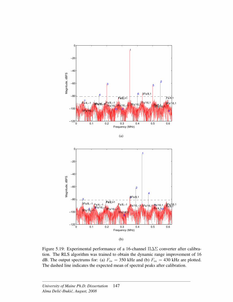
0 0.1 0.2 0.3 0.4 0.5 0.6−120
−100
−80
−60
−40
−20
0
Frequency (MHz)
Mag
nitu
de, d
BFS
1
23
4
5
6
7
89
10
Fs/16,1Fs/16,−1 Fs/8,1
Fs/8,−1 3Fs/16,13Fs/16,−1
Fs/4,1
Fs/4,−15Fs/16,1
5Fs/16,−1
3Fs/8,1
3Fs/8,−1 7Fs/16,17Fs/16,−1
Fs/2,1Fs/2,−1
(a)
0 0.1 0.2 0.3 0.4 0.5 0.6−120
−100
−80
−60
−40
−20
0
Frequency (MHz)
Mag
nitu
de, d
BFS
1
2
3
45
67
8
9 10Fs/16,1Fs/16,−1 Fs/8,1
Fs/8,−1 3Fs/16,1
3Fs/16,−1 Fs/4,1Fs/4,−1 5Fs/16,1
5Fs/16,−1
3Fs/8,1
3Fs/8,−1
7Fs/16,1
7Fs/16,−1
Fs/2,1Fs/2,−1
(b)
Figure 5.19: Experimental performance of a 16-channel Π∆Σ converter after calibra-tion. The RLS algorithm was trained to obtain the dynamic range improvement of 16dB. The output spectrums for: (a) Fin = 350 kHz and (b) Fin = 430 kHz are plotted.The dashed line indicates the expected mean of spectral peaks after calibration.
University of Maine Ph.D. DissertationAlma Delic-Ibukic, August, 2008
147
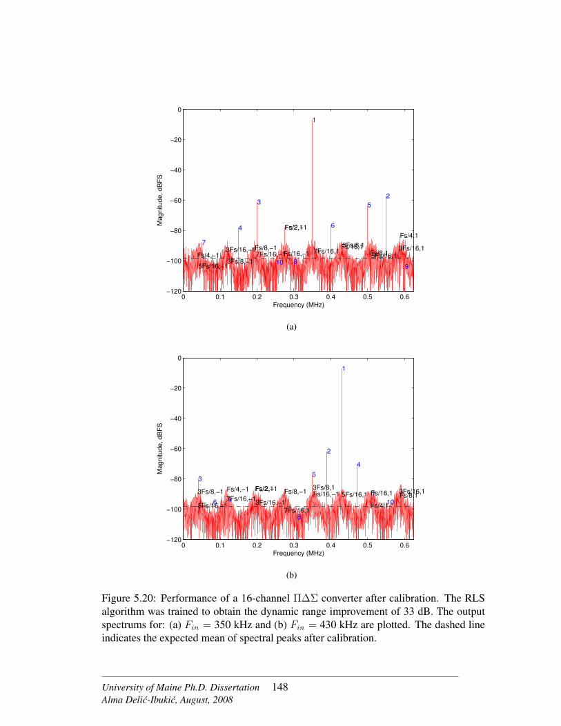
0 0.1 0.2 0.3 0.4 0.5 0.6−120
−100
−80
−60
−40
−20
0
Frequency (MHz)
Mag
nitu
de, d
BFS
1
23
4
5
6
7
89
10
Fs/16,1Fs/16,−1 Fs/8,1
Fs/8,−1 3Fs/16,13Fs/16,−1
Fs/4,1
Fs/4,−1 5Fs/16,1
5Fs/16,−1
3Fs/8,1
3Fs/8,−1
7Fs/16,17Fs/16,−1
Fs/2,1Fs/2,−1
(a)
0 0.1 0.2 0.3 0.4 0.5 0.6−120
−100
−80
−60
−40
−20
0
Frequency (MHz)
Mag
nitu
de, d
BFS
1
2
3
45
67
8
9 10Fs/16,1Fs/16,−1 Fs/8,1Fs/8,−1 3Fs/16,1
3Fs/16,−1 Fs/4,1
Fs/4,−15Fs/16,1
5Fs/16,−1
3Fs/8,13Fs/8,−1
7Fs/16,1
7Fs/16,−1Fs/2,1Fs/2,−1
(b)
Figure 5.20: Performance of a 16-channel Π∆Σ converter after calibration. The RLSalgorithm was trained to obtain the dynamic range improvement of 33 dB. The outputspectrums for: (a) Fin = 350 kHz and (b) Fin = 430 kHz are plotted. The dashed lineindicates the expected mean of spectral peaks after calibration.
University of Maine Ph.D. DissertationAlma Delic-Ibukic, August, 2008
148

skew errors occur at
fε,∆t = iFSM± FIN , i = 1, 2, 3...M/2. (5.12)
In (5.12), FS is the Nyquist-rate clock, FIN is the input frequency and M is the number
of channels in a parallel configuration.
Even though the frequency locations of the clock skew and gain error spectrum
peaks are the same, the distortion terms in Figure 5.20 that are left after the gain calibra-
tion was performed are most likely due to clock skew error. The Π∆Σ ADC test setup
utilizes two separate chips to form a 16-channel Π∆Σ converter. Due to this configura-
tion there may exist a clock skew between the two chips that is more dominant than a
clock skew between the channels within a single chip. To confirm that a clock skew be-
tween the two chips is enough to cause distortion tones seen in Figure 5.20, a 16-channel
Π∆Σ converter with an additional channel for calibration was modelled in MATLAB.
Each channel contains 2nd order ∆Σ modulator, the decimation filter described by (4.15)
and a quantizer that mimics the quantization noise seen in the experiment (σ2v = 6 ·10−9
V2). The quantizer was modelled as an additive white noise source. The oversampling
ratio D and the Nyquist-rate frequency FS were set to 4 and 1.25 MHz, respectively.
This was the same as in the experiment. A fixed clock skew error of 0.2% at over-
sampled clock period (Tclk = 1DFS
) was introduced in eight channels. This mimics the
constant clock delay that may be seen between the two chips on the test board. Also,
a gain error mismatches of 0.5% were introduced in all 16 channels including the cali-
bration channel. Figure 5.21 shows the simulated spectrum for uncalibrated 16-channel
Π∆Σ converter with gain and clock skew errors at 350 kHz and 430 kHz. Because the
spectrum peaks due to gain errors and clock skew errors occur at the same location it
is hard to distinguish between the two. The dashed line indicates the expected mean of
spectral peaks due to 0.5% channel gain mismatches. As was the case in the experi-
University of Maine Ph.D. DissertationAlma Delic-Ibukic, August, 2008
149

0 0.1 0.2 0.3 0.4 0.5 0.6−120
−100
−80
−60
−40
−20
0
Frequency (MHz)
Mag
nitu
de, d
BFS
Fs/16,1Fs/16,−1
Fs/8,1Fs/8,−1
3Fs/16,1
3Fs/16,−1
Fs/4,1Fs/4,−1
5Fs/16,1
5Fs/16,−1
3Fs/8,13Fs/8,−1
7Fs/16,17Fs/16,−1
Fs/2,1Fs/2,−1
(a)
0 0.1 0.2 0.3 0.4 0.5 0.6−120
−100
−80
−60
−40
−20
0
Frequency (MHz)
Mag
nitu
de, d
BFS
Fs/16,1
Fs/16,−1
Fs/8,1Fs/8,−1
3Fs/16,13Fs/16,−1
Fs/4,1Fs/4,−1
5Fs/16,1
5Fs/16,−1
3Fs/8,13Fs/8,−1
7Fs/16,17Fs/16,−1
Fs/2,1Fs/2,−1
(b)
Figure 5.21: Simulated output spectrum for uncalibrated 16-channel Π∆Σ converterwith (a) Fin = 350kHz and (b) Fin = 430 kHz. The clock skew of 0.2% of a high ratesampling period is simulated between the two chips. The dashed line corresponds to atheoretical mean of spectral peaks caused by channel gain mismatches.
University of Maine Ph.D. DissertationAlma Delic-Ibukic, August, 2008
150

0 0.1 0.2 0.3 0.4 0.5 0.6−120
−100
−80
−60
−40
−20
0
Frequency (MHz)
Mag
nitu
de, d
BFS
Fs/16,1Fs/16,−1
Fs/8,1
Fs/8,−1 3Fs/16,1
3Fs/16,−1
Fs/4,1Fs/4,−1 5Fs/16,1
5Fs/16,−1
3Fs/8,13Fs/8,−1
7Fs/16,17Fs/16,−1
Fs/2,1Fs/2,−1
(a)
0 0.1 0.2 0.3 0.4 0.5 0.6−120
−100
−80
−60
−40
−20
0
Frequency (MHz)
Mag
nitu
de, d
BFS
Fs/16,1Fs/16,−1
Fs/8,1
Fs/8,−1
3Fs/16,1
3Fs/16,−1
Fs/4,1Fs/4,−1
5Fs/16,15Fs/16,−1
3Fs/8,1
3Fs/8,−17Fs/16,17Fs/16,−1
Fs/2,1Fs/2,−1
(b)
Figure 5.22: Simulation results for a 16-channel Π∆Σ converter after calibration. TheRLS algorithm was trained to obtain the dynamic range improvement of 16 dB. Theoutput spectrums for: (a) Fin = 350 kHz and (b) Fin = 430 kHz are plotted. The dashedline indicates the expected mean of spectral peaks after calibration.
University of Maine Ph.D. DissertationAlma Delic-Ibukic, August, 2008
151

0 0.1 0.2 0.3 0.4 0.5 0.6−120
−100
−80
−60
−40
−20
0
Frequency (MHz)
Mag
nitu
de, d
BFS
Fs/16,1Fs/16,−1
Fs/8,1
Fs/8,−1
3Fs/16,1
3Fs/16,−1 Fs/4,1Fs/4,−1
5Fs/16,1
5Fs/16,−1
3Fs/8,1
3Fs/8,−1 7Fs/16,17Fs/16,−1
Fs/2,1Fs/2,−1
(a)
0 0.1 0.2 0.3 0.4 0.5 0.6−120
−100
−80
−60
−40
−20
0
Frequency (MHz)
Mag
nitu
de, d
BFS
Fs/16,1
Fs/16,−1Fs/8,1
Fs/8,−13Fs/16,13Fs/16,−1
Fs/4,1
Fs/4,−1
5Fs/16,1
5Fs/16,−1
3Fs/8,13Fs/8,−1
7Fs/16,17Fs/16,−1
Fs/2,1Fs/2,−1
(b)
Figure 5.23: Simulation results for a 16-channel Π∆Σ converter after calibration. TheRLS algorithm was trained to obtain the dynamic range improvement of 33 dB. Theoutput spectrums for: (a) Fin = 350 kHz and (b) Fin = 430 kHz are plotted. The dashedline indicates the expected mean of spectral peaks after calibration.
University of Maine Ph.D. DissertationAlma Delic-Ibukic, August, 2008
152

mental run, the signal to noise ratio σ2w/σ
2v of 42 dB was used to aid in calibration of
a 16-channel Π∆Σ converter. The RLS algorithm convergence was stopped once the
mean-squared error Q[n] reached -62 dB and -79 dB for dynamic range improvements
of 16 dB and 33 dB, respectively. Figures 5.22 and 5.23 show the output spectrums
for a 16-channel Π∆Σ converter after calibration for dynamic range improvement of
16 dB and 33 dB, respectively. The dashed line indicates the expected mean of spectral
peaks due to channel gain mismatches after calibration. The distortion tones observed
in Figure 5.20 are also present in Figure 5.23. Because the only other errors introduced
in simulations are due to clock skew, it is suspected that the distortion terms left after
gain calibration are due to clock skew seems plausible.
Aside from timing errors, for a given signal to noise ratio σ2w/σ
2v , the RLS algo-
rithm continued converging according to (4.63) and the dynamic range of the converter
before and after calibration improved according to findings in Section 4.9.
University of Maine Ph.D. DissertationAlma Delic-Ibukic, August, 2008
153

CHAPTER 6
Conclusion
In this thesis, two digital background calibration techniques were developed to
aid in improving the linearity of high-resolution, wide bandwidth ADCs. The goal was
to develop a fully digital calibration technique that has minimal intrusion to the overall
A/D converter architecture and does not interrupt the normal operation of the converter
(i.e. runs continuously in the background). The two converter architectures considered
were pipeline and Π∆Σ ADCs.
Pipeline architecture converters offer wide-bandwidth but their resolution, if not
calibrated, is limited to approximately 10-12 bits. This is because pipeline converters
rely on high-precision analog components such as high-gain operation amplifiers. As
CMOS technologies are scaled to smaller geometries, the design of high-precision ana-
log components becomes increasingly difficult due to the reduced power-supply volt-
ages which put the limit on the number of cascoding levels that can occur in a given
circuit. On the other hand, Π∆Σ converters utilize parallelism to increase the bandwidth
of oversampling ∆Σ modulators that inherently offer high-resolution. However, Π∆Σ
converters offer high-resolution and wide bandwidth results only if all of the channels
in parallel configuration are identical and modulation sequences are in-sync. Because
the channel mismatches are usually caused by variations in the manufacturing process,
the decline in the overall performance of Π∆Σ converters may be inevitable.
As the CMOS technologies are scaled to smaller geometries, the design of ana-
log circuit elements becomes increasingly difficult due to reduced power supply voltages
that put a limit on the number of cascoding levels that can occur in a given circuit. On
the other hand, the digital circuitry adjusts readily to scaled process technologies and
occupies less area on silicon. Due to this, the digital calibration techniques are more
favorable when improving the performance of A/D converters.
University of Maine Ph.D. DissertationAlma Delic-Ibukic, August, 2008
154

The accomplishments of these thesis and recommendations for future work are
summarized next.
6.1 Summary of Accomplishments
The first accomplishment of this thesis was the development of digital back-
ground calibration technique that is suitable for implementation in a fully monolithic
pipeline A/D converters. The developed technique is discussed in Chapter 3. The new
scheme utilizes an existing digital calibration algorithm developed by Karanicolas et.
al. [28] and extends it to work in real-time by incorporating two additional stages lo-
cated at the end of the pipeline. The theory and results of this work were published
in [55, 56]. At the time of its publication, other digital background calibration tech-
niques were reported in [25,44,45]. These are correlation-based background calibration
techniques, where a random signal is introduced in a pipeline stage and stage error terms
are measured in digital domain by removing the introduced random term. Calibration
techniques in [25, 45] rely on complex digital post-processing for extraction of calibra-
tion parameters and are slow to converge. Also, in [25] the calibration technique is de-
pendant on the input signal statistics. In addition to the required digital post-processing
in [44], an additional pipeline converter identical to the one being calibrated is required.
If not perfectly matched, the two ADCs will have an additional error sources due to
channel mismatches. The work presented in this thesis frees one conversion cycle for
calibration purposes by introducing two extra stages at the end of the pipeline. Once the
conversion cycle is available, a pipeline stage can be calibrated according to [28]. To
calibrate the first seven stages of a 16-stage pipeline A/D converter implemented using
1-bit/stage topology, a total of 154 clock cycles are needed and calibration is indepen-
dent of input signal statistics. The algorithm is successful in correcting for comparator
offset, charge injection, and capacitor mismatch errors [28].
A hardware model of the continuous digital calibration logic was designed using
University of Maine Ph.D. DissertationAlma Delic-Ibukic, August, 2008
155
VHDL, and it was effective in showing the success of the proposed technique. The
proposed calibration technique is completely digital, transparent to the overall system,
and applicable to multiple bits per stage pipeline architectures. The additional stages
at the end of the pipeline are used only during the calibration process. The VHDL was
used to model the real-time calibration scheme, and hardware simulation was performed
using Verilog-XL.
The simulation results verified the success of the derived calibration scheme.
Calibration was demonstrated using a 14-bit pipeline ADC with a 1-bit/stage architec-
ture and 16 identical stages. The first seven (and most critical) stages in the pipeline
were calibrated. For the simulated ADC, the number of effective bits was improved by
at least 2-bits, and the dynamic range of the converter was extended by at least 20 dB.
The required area to implement the necessary digital logic scales down easily with the
new process technologies, making it an attractive solution for improving the resolution
of the pipeline converters. If the power consumption is of a major concern, the power
dedicated to calibration can be minimized by running the calibration logic periodically
instead of continuously.
The second accomplishment of this thesis was the development of digital back-
ground calibration scheme to calibrate channel gain errors in Π∆Σ converters. The
theory and simulation results behind the developed technique are discussed in Chap-
ter 4. Also, to demonstrate the developed calibration technique in hardware, a chip
containing ten second-order ∆Σ modulators was designed and fabricated in a 0.5-µm
CMOS process technology. The hardware results are discussed in Chapter 5. The
work completed has been reported in [58]. At the time of its publication, other rele-
vant digital background calibration techniques applicable to Π∆Σ converters have been
reported [31,80]. In [31] an additional channel is used as a reference element. The chan-
nel being calibrated is placed in parallel with the reference element and calibration is
performed in digital domain through the use of of digital post-processing. The accuracy
University of Maine Ph.D. DissertationAlma Delic-Ibukic, August, 2008
156

of the calibration is limited by the time slot (number of samples) required for calibra-
tion. Because all of the samples in the time slot are required for calibration at one time,
the hardware complexity increases as the calibration accuracy improves. Calibration of
the overall system depends on the number of channels and the time required to calibrate
a single channel. The calibration technique in [80] uses an adaptive algorithm to correct
for channel mismatches. The channel mismatches errors (gain and offset) are corrected
relative to the first A/D converter in the parallel configuration. In order to converge, the
calibration algorithm assumes the same input statistics for all channels.
The proposed calibration requires an extra channel that is linearly dependant on
Π∆Σ channels used. The redundancy in the system allows for the gain errors within the
channels to be successfully corrected. To solve for gain correction terms, the adaptive
RLS algorithm can be used. All the channels are calibrated simultaneously, calibration
is transparent to the overall system and is independent of the input statistics. The time
required to calibrate the overall system depends on the convergence rate of the adaptive
RLS algorithm.
Channel gain and offset mismatch errors that occur in Π∆Σ converter architec-
tures were defined and discussed. The theory behind calibration algorithm was derived
and the RLS algorithm performance when applied to Π∆Σ converters was discussed
in detail. When applied to Π∆Σ ADCS, the RLS algorithm performance is limited by
the signal-to-noise ratio that is observed at the output of each channel in the parallel
configuration before demodulation. Table 6.1 gives a summary of the RLS algorithm
convergence findings when applied to Π∆Σ ADCs. Using MATLAB, an 8-channel
Π∆Σ converter with additional channel for calibration was simulated to confirm the
findings in Table 6.1.
Also, the relationship between the RLS algorithm convergence and the improve-
ment in the dynamic range of a Π∆Σ converter was derived and confirmed using MATA-
LAB simulations. An 8-channel and 16-channel Π∆Σ converter with an extra channel
University of Maine Ph.D. DissertationAlma Delic-Ibukic, August, 2008
157
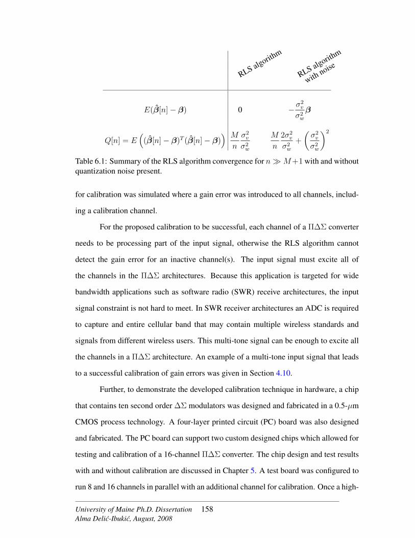
RLS algorithm
RLS algorithm
withnoise
E(β[n]− β) 0 − σ2v
σ2w
β
Q[n] = E(
(β[n]− β)T (β[n]− β)) M
n
σ2v
σ2w
M
n
2σ2v
σ2w
+
(σ2v
σ2w
)2
Table 6.1: Summary of the RLS algorithm convergence for n�M+1 with and withoutquantization noise present.
for calibration was simulated where a gain error was introduced to all channels, includ-
ing a calibration channel.
For the proposed calibration to be successful, each channel of a Π∆Σ converter
needs to be processing part of the input signal, otherwise the RLS algorithm cannot
detect the gain error for an inactive channel(s). The input signal must excite all of
the channels in the Π∆Σ architectures. Because this application is targeted for wide
bandwidth applications such as software radio (SWR) receive architectures, the input
signal constraint is not hard to meet. In SWR receiver architectures an ADC is required
to capture and entire cellular band that may contain multiple wireless standards and
signals from different wireless users. This multi-tone signal can be enough to excite all
the channels in a Π∆Σ architecture. An example of a multi-tone input signal that leads
to a successful calibration of gain errors was given in Section 4.10.
Further, to demonstrate the developed calibration technique in hardware, a chip
that contains ten second order ∆Σ modulators was designed and fabricated in a 0.5-µm
CMOS process technology. A four-layer printed circuit (PC) board was also designed
and fabricated. The PC board can support two custom designed chips which allowed for
testing and calibration of a 16-channel Π∆Σ converter. The chip design and test results
with and without calibration are discussed in Chapter 5. A test board was configured to
run 8 and 16 channels in parallel with an additional channel for calibration. Once a high-
University of Maine Ph.D. DissertationAlma Delic-Ibukic, August, 2008
158

data rate digital outputs from the two chips were collected, digital filtering, decimation,
demodulation, channel recombination and calibration were executed in MATLAB. The
experimental results were successful in demonstrating the importance of channel gain
error calibration and they are in the agreement with the theory derived in Section 4.9.
6.2 Recommendations for Future Work
To demonstrate the background calibration technique for pipeline ADCs in hard-
ware requires additional research. This can be accomplished by designing a 14-bit ADC
with 1-bit per stage topology, gains less than two and intermediate bits as the outputs
of the converter. Additional digital input lines for each calibrated stage must also be
provided in order to allow the calibration logic to specify the digital stage outputs, or
ground the stage inputs. These could provide inputs to an FPGA (Field Programmable
Gate Array) where the continuous digital calibration and error correction logic resides.
This way the power consumption of the digital calibration logic can be examined, and
the effectiveness of the derived calibration in hardware evaluated.
The gain calibration technique for Π∆Σ converters was successfully demon-
strated. However, there are other errors in this architecture that degrade the performance
of the overall converter. These include channel offset errors that if present in a channel
will show up in the output spectrum as discussed in Section 4.3, and timing errors (clock
skew). Additional research is required to remove these errors.
Also, the chip that contains ten ∆Σ modulators was already designed, fabri-
cated and tested. After the high-rate digital data was collected by the logic analyzer,
digital filtering, decimation, calibration and recombination were done in software. To
further test the implementation, effectiveness and power consumption of the required
calibration set-up, all the work currently implemented in software can be transferred
to an FPGA so the digital signal processing and calibration algorithm can be evalu-
ated. For the current test set-up, Hadamard modulation sequences are generate using
University of Maine Ph.D. DissertationAlma Delic-Ibukic, August, 2008
159

an FPGA Evaluation Platform ML-401 Virtex-4. To calibrate a 16-channel Π∆Σ con-
verter, sixteen Hadamard sequences need to be generated plus and additional sequence
for calibration channel. The ML-401 evaluation board provides 32 single-ended signal
connections to the FPGA I/Os. To provide the fabricated chip with the modulation se-
quences and collected the high-rate digital data for further processing in an FPGA, at
least 34 connections are needed. This is if a 16-channel Π∆Σ converter is to be tested.
For an 8-channel converter, the FPGA ML-401 evaluation board will be sufficient.
Further, the fabricated chip was designed to run at 50 MHz, but all the exper-
imental results were collected at 5 MHz. Testing at higher frequencies provided the
output spectrum that resembles the results when Hadamard modulation and demodula-
tion sequences are not aligned correctly. Hadamard modulation sequences are available
for a full, high-rate clock cycle Tclk, and on chip they are latched on φ2 (Tφ2 = Tclk/2).
It is assumed that Hadamard modulation sequences are stable by the time φ2 occurs. If
this is not the case, the input signal will be modulated with a wrong Hadamard sequence,
which in turn will affect demodulation and the final answer. Because there is no access
to φ2, it is difficult to determine if the data is captured correctly. One way to deal with
this would be by trial and error, where a Hadamard modulation sequence coming from
an FPGA can be delayed until a sequence is captured.
University of Maine Ph.D. DissertationAlma Delic-Ibukic, August, 2008
160

REFERENCES
[1] Digital cellular telecommunications system (Phase 2+); Radio transmission andreception (GSM 05.05 version 8.5.1 Release 1999), ETSI EN 300 910 V8.5.1(2000-11) ed., European Telecommunications Standards Institute, Nov. 2000.
[2] A. K. Salkintzis, H. Nie, and P. T. Mathiopoulos, “ADC and DSP challenges inthe development of software radio base stations,” IEEE Personal Communica-tions, pp. 47–55, Aug. 1999.
[3] A. Perez-Neira, X. Mester, and J. R. Fonollosa, “Smart antennas in software radiobase stations,” IEEE Communications Magazine, pp. 166–173, Feb. 2001.
[4] K. C. Zangi and R. D. Koilpillai, “Software radio issues in cellular base stations,”IEEE Journal on Selected Areas in Communications, vol. 17, pp. 561–573, Apr.1999.
[5] J. Mitola III, “Technical challengies in the globalization of software radio,” IEEECommunications Magazine, pp. 84–87, Feb. 1999.
[6] R. H. Walden, “Analog-to-digital converter survey and analysis,” IEEE Journalon Selected Areas in Communications, vol. 17, pp. 539–548, Apr. 1999.
[7] J. Li and U.-K. Moon, “A 1.8-V 67-mW 10-bit 100-MS/s pipelined ADC usingtime-shifted CDS technique,” IEEE Journal of Solid-State Circuits, vol. 39, pp.1468–1476, Sept. 2004.
[8] Y.-T. Wang and B. Razavi, “An 8-bit 150-MHz CMOS A/D converter,” IEEEJournal of Solid-State Circuits, vol. 35, pp. 308–317, Mar. 2000.
[9] S.-M. Yoo, J.-B. Park, S.-H. Lee, and U.-K. Moon, “A 1.8-V 67-mW 10-bit 100-MS/s pipelined ADC using time-shifted CDS technique,” IEEE Transactions onCircuits and System-II, vol. 51, pp. 269–275, May 2004.
[10] K. Y. Kim, N. Kusayanagi, and A. A. Abidi, “A 10-b, 100-MS/s CMOS A/Dconverter,” IEEE Journal of Solid-State Circuits, vol. 32, pp. 302–311, Mar. 1997.
[11] W. Yang, D. Kelly, I. Mehr, M. T. Sayuk, and L. Singer, “A 3-V 340-mW 14-b75-Msample/s CMOS ADC with 85-dB SFDR at Nyquist input,” IEEE Journalof Solid-State Circuits, vol. 36, pp. 1931–1936, Dec. 2001.
[12] I. Fujimori, K. Koyama, D. Trager, F. Tam, and L. Longo, “A 5-V single-chipdelta-sigma audio A/D converter with 111 dB dynamic range,” IEEE Journal ofSolid-State Circuits, vol. 32, pp. 329–336, Mar. 1997.
[13] R. Schreier and G. C. Temes, Understanding Delta-Sigma Data Converters.Hoboken, NJ: John Wiley & Sons, Inc, 2005.
University of Maine Ph.D. DissertationAlma Delic-Ibukic, August, 2008
161

[14] S. Saucier, “Multiband analog-to-digital conversion,” Master’s thesis, Universityof Maine, Orono, Dec. 2002. [Online]. Available: http://www.eece.maine.edu/∼hummels/thesis/ssaucier 02.pdf
[15] R. F. Cormier, T. L. Sculley, and R. H. Bamberger, “Combining subband decom-position and sigma delta modulation for wideband A/D conversion,” in Proceed-ings of IEEE International Symposium on Circuits and Systems, May 1994, pp.357–360.
[16] R. Khoini-Poorfard, L. B. Lim, and D. A. Johns, “Time-interleaved oversam-pling A/D converters: Theory and practice,” IEEE Transactions on Circuits andSystems-II, vol. 44, pp. 634–645, Aug. 1997.
[17] A. Eshraghi and T. S. Fiez, “A time-interleaved parallel ∆Σ A/D converter,” IEEETransactions on Circuits and Systems-II, vol. 50, pp. 118–129, Mar. 2003.
[18] I. Galton and H. T. Jensen, “Delta-sigma modulator based on A/D conversionwithout oversampling,” IEEE Transactions on Circuits and Systems-II, vol. 42,pp. 773–784, Dec. 1995.
[19] ——, “Oversampling parallel delta-sigma modulator A/D conversion,” IEEETransactions on Circuits and Systems-II, vol. 43, pp. 801–810, Dec. 1996.
[20] A. Eshraghi and T. S. Fiez, “A comparative analysis of parallel delta-sigma ADCarhitectures,” IEEE Transactions on Circuits and Systems-II, vol. 51, pp. 450–458, Mar. 2004.
[21] J. M. Ingino and B. A. Wooley, “A continuously calibrated 12-b, 10-MS/s, 3.3VA/D converter,” IEEE Journal of Solid-State Circuits, vol. 12, pp. 1920–1931,Dec. 1998.
[22] K. Dyer, D. Fu, S. Lewis, and P. Hurst, “An analog background calibration tech-nique for time-interleaved analog-to-digital converters,” IEEE Journal of Solid-State Circuits, vol. 33, pp. 1912–1919, Dec. 1998.
[23] M. Taherzadeh-Sani and A. A. Hamoui, “Digital background calibration ofcapacitor-mismatch error in pipelined ADCs,” IEEE Transactions on Circuits andSystems-II, vol. 53, pp. 966–970, Sept. 2006.
[24] H.-C. Liu, Z.-M. Lee, and J.-T. Wu, “A 15-bit 40-MS/s CMOS pipelined analog-to-digital converter with digital background calibration,” IEEE Journal of Solid-State Circuits, vol. 40, pp. 1047–1056, May 2005.
[25] B. Murmann and B. E. Boser, “A 12-bit 75-MS/s pipelined ADC using open-loopresidue amplification,” IEEE Journal of Solid-State Circuits, vol. 38, pp. 2040–2050, Dec. 2003.
University of Maine Ph.D. DissertationAlma Delic-Ibukic, August, 2008
162

[26] J. McNeill, M. Coln, and B. Larivee, “Split-ADC arhictecture for deterministicdigital background calibration of a 16b 1MS/s ADC,” IEEE Journal of Solid-StateCircuits, vol. 40, pp. 2437–2445, Dec. 2005.
[27] E. G. Soenen and R. L. Geiger, “An architecture and an algorithm for fully digitalcorrection of monolithic pipelined ADC’s,” IEEE Transactions on Circuits andSystems-II, vol. 42, pp. 143–153, Mar. 1995.
[28] A. N. Karanicolas, H.-S. Lee, and K. L. Bacrania, “A 15-b 1-Msample/s digitallyself-calibrated pipeline ADC,” IEEE Journal of Solid-State Circuits, vol. 28, pp.1207–1215, Dec. 1993.
[29] D. Fu, K. Dyer, S. Lewis, and P. Hurst, “A digital background calibration tech-nique for time-interleaved analog-to-digital converters,” IEEE Journal of Solid-State Circuits, vol. 33, pp. 1904–1911, Dec. 1998.
[30] R. D. Batten, A. Eshraghi, and T. S. Fiez, “Calibration of parallel ∆Σ ADCs,”IEEE Transactions on Circuits and Systems-II, vol. 49, pp. 390–399, June 2002.
[31] V. Ferragina, A. Fornasari, U. Gatti, P. Malcovati, and F. Maloberti, “Gain andoffset mismatch calibration in time-interleaved multipath A/D sigma-delta mod-ulators,” IEEE Transactions on Circuits and Systems-I, vol. 51, pp. 2365–2373,Dec. 2004.
[32] R. G. Massolini, G. Cesura, and R. Castello, “A fully digital fast convergencealgorithm for nonlinearity correction in multistage ADC,” IEEE Transactions onCircuits and Systems-II, vol. 53, pp. 389–393, May 2006.
[33] E. B. Blecker, T. M. McDonald, O. E. Erdogan, P. J. Hurst, and S. H. Lewis, “Dig-ital background calibration of an algorithmic analog-to-digital converter using asimplified queue,” IEEE Journal of Solid-State Circuits, vol. 38, pp. 1059–1062,June 2003.
[34] H.-S. Lee, D. A. Hodges, and P. R. Gray, “A self-calibrated 15 bit CMOS A/Dconverter,” IEEE Journal of Solid-State Circuits, vol. 6, pp. 813–819, Dec. 1984.
[35] J. Ming and S. H. Lewis, “An 8-bit 80-Msample/s pipelined analog-to-digital con-verter with background calibration,” IEEE Journal of Solid-State Circuits, vol. 36,pp. 1489–1497, Oct. 2001.
[36] Y.-M. Lin, B. Kim, and P. R. Gray, “A 13-b 2.5-MHz self-calibrated pipelinedA/D converter in 3-micron CMOS,” IEEE Journal of Solid-State Circuits, vol. 26,pp. 628–636, Apr. 1991.
[37] H. van der Ploeg, G. Hoogzaad, H. A. H. Termeer, M. Vertregt, and R. L. J.Roovers, “A 2.5-V 12-b 54-Msample/s 0.25-µm CMOS ADC in 1-mm2 withmixed-signal chopping and calibration,” IEEE Journal of Solid-State Circuits,vol. 36, pp. 1859–1867, Dec. 2001.
University of Maine Ph.D. DissertationAlma Delic-Ibukic, August, 2008
163

[38] H.-S. Lee, “A 12-b 600 ks/s digitally self-calibrated pipelined algorithmic ADC,”IEEE Journal of Solid-State Circuits, vol. 29, pp. 509–515, Apr. 1994.
[39] I. E. Opris, L. D. Lewicki, and B. C. Wong, “A single-ended 12-bit 20 Msample/sself-calibrating pipeline A/D converter,” IEEE Journal of Solid-State Circuits,vol. 33, pp. 1898–1903, Dec. 1998.
[40] K. Iizuka, H. Matsui, M. Ueda, and M. Daito, “A 14-bit digitally self-calibratedpipelined ADC with adaptive bias optimization for arbitrary speeds up to 40MS/s,” IEEE Journal of Solid-State Circuits, vol. 41, pp. 883–890, Apr. 2006.
[41] C. R. Grace, P. J. Hurst, and S. H. Lewis, “A 12-bit 80-MSample/s pipelinedADCwith bootstrapped digital calibration,” IEEE Journal of Solid-State Circuits,vol. 40, pp. 1038–1046, May 2005.
[42] T.-H. Shu, B.-S. Song, and K. Bacrania, “A 13-b 10-Msample/s ADC digitallycalibrated with oversampling delta-sigma converter,” IEEE Journal of Solid-StateCircuits, vol. 30, pp. 443–452, Apr. 1995.
[43] U.-K. Moon and B.-S. Song, “Background digital calibration techniques forpipelined ADC’s,” IEEE Transactions on Circuits and Systems-II, vol. 44, pp.102–109, Feb. 1997.
[44] J. Li and U.-K. Moon, “Background calibration techniques for multistagepipelined ADCs with digital redundacy,” IEEE Transactions on Circuits andSystems-II, vol. 50, pp. 531–538, Sept. 2003.
[45] J. P. Keane, P. J. Hurst, and S. H. Lewis, “Background interstage gain calibrationtechnique for pipelined ADCs,” IEEE Transactions on Circuits and Systems-I,vol. 52, pp. 32–43, Jan. 2005.
[46] X. Wang, P. Hurst, and S. Lewis, “A 12-bit 20 MS/s pipelined ADC with nesteddigital background calibration,” in Proceedings of IEEE Custom IC Conf., SanJose, Sept. 2003, pp. 409–412.
[47] A. Abo, “Design for reliability of low-voltage switched-capacitor circuits,” Ph.D.dissertation, University of California, Berkeley, California, May 1999.
[48] M. Waltari, “Circuit techniques for low-voltage and high-speed A/D converters,”Ph.D. dissertation, Helskinki University of Technology, Helsinki, Finland, May2002.
[49] (2007) International Technology Roadmap for Semiconductors 2007 Update.[Online]. Available: http://www.itrs.net
[50] Y. Chiu, C. W. Tsang, B. Nikolic, and P. R. Gray, “Least mean square adaptivedigital background calibration of pipelined analog-to-digital converters,” IEEETransactions on Circuits and Systems-I, vol. 51, pp. 38–46, Jan. 2004.
University of Maine Ph.D. DissertationAlma Delic-Ibukic, August, 2008
164

[51] S. Huang and B. C. Levy, “Blind calibration of timing offset for four-channeltime-interleaved ADCs,” IEEE Transactions on Circuits and Systems-I, vol. 54,pp. 863–876, Apr. 2007.
[52] ——, “Adaptive blind calibration of timing offset and gain mismatch for two-channel time-interleaved ADCs,” IEEE Transactions on Circuits and Systems-I,vol. 53, pp. 1278–1288, June 2006.
[53] Z.-M. Lee, C.-Y. Wang, and J.-T. Wu, “A CMOS 15-bit, 125-MS/s time-interleaved ADC with digital background calibration,” IEEE Journal of Solid-State Circuits, vol. 42, pp. 2149–2160, Oct. 2007.
[54] S. M. Jamal, D. Fu, N. C.-J.Chang, P. J. Hurst, and S. H. Lewis, “A 10-b 120-Msample/s time-interleaved analog-to-digital converter with digital backgroundcalibration,” IEEE Journal of Solid-State Circuits, vol. 37, pp. 1618–1627, Dec.2002.
[55] A. Delic-Ibukic and D. M. Hummels, “Continuous digital calibration of pipelineA/D converters,” in Proceedings of IEEE International Instrumentation and Mea-surement Technology Conference, May 2005, pp. 2–6.
[56] ——, “Continuous digital calibration of pipeline A/D converters,” IEEE Transac-tions on Instrumentation and Measurement, vol. 55, pp. 1175–1185, Aug. 2006.
[57] A. Delic-Ibukic, “Continuous digital calibration of pipeline A/D converters,”Master’s thesis, University of Maine, Orono, May 2004. [Online]. Available:http://www.eece.maine.edu/∼hummels/thesis/adi 04.pdf
[58] A. Delic-Ibukic and D. M. Hummels, “Continuous gain calibration of paralleldelta sigma A/D converters,” in Proceedings of IEEE International Instrumenta-tion and Measurement Technology Conference, Apr. 2006, pp. 905–909.
[59] H. Nyquist, “Certain topics in telegraph transmission theory,” Reprint as classicpaper in Proc. of the IEEE, vol. 90, pp. 280–305, Feb. 2002.
[60] C. E. Shannon, “Communication in the presence of noise,” Reprint as classicpaper in Proc. of the IEEE, vol. 86, pp. 447–457, Feb. 1998.
[61] (2007) Analog Devices Inc. [Online]. Available: http://www.analog.com/
[62] (2007) Texas Instruments Inc. [Online]. Available: http://www.ti.com/
[63] S. R. Norsworthy, R. Schreier, and G. C. Temes, Delta-Sigma Data converters:Theory, Design, and Simulation. Hoboken, NJ: John Wiley & Sons, Inc, 1997.
[64] E. T. King, A. Eshraghi, I. Galton, and T. S. Fiez, “A Nyquist-rate delta-sigmaA/D converter,” IEEE Journal of Solid-State Circuits, vol. 33, pp. 45–52, Jan.1998.
University of Maine Ph.D. DissertationAlma Delic-Ibukic, August, 2008
165

[65] S. Limotyrakis, S. D. Kulchycki, D. K. Su, and B. A. Wooley, “A 150-MS/s 8-b 71-mW CMOS time-interleaved ADC,” IEEE Journal of Solid-State Circuits,vol. 40, pp. 1057–1067, May 2005.
[66] L. Sumanen, M. Waltari, and K. A. I. Halonen, “A 10-bit 200-MS/s CMOS par-allel pipeline A/D converter,” IEEE Journal of Solid-State Circuits, vol. 36, pp.1048–1055, July 2001.
[67] M. Kozak and I. Kale, “Novel topologies for time-interleaved delta-sigma modu-lators,” IEEE Transactions on Circuits and Systems-II, vol. 47, pp. 639–654, July2000.
[68] G. Bernardinis, F. Borghetti, V. Ferragina, A. Fornasari, U. Gatti, P. Malcovati,and F. Maloberti, “A wide-band 280-MHz four-path time-interleaved bandpasssigma-delta modulator,” IEEE Transactions on Circuits and Systems-I, vol. 53,pp. 1423–1432, July 2006.
[69] W. C. Black Jr. and D. A. Hodges, “Time interleaved converter arrays,” IEEEJournal of Solid-State Circuits, vol. SC-15, pp. 1022–1029, Dec. 1980.
[70] A. Petraglia and S. K. Mitra, “Analysis of mismatch effect among A/D converterin a time-interleaved waveform digitizer,” IEEE Transactions on Instrumentationand Measurement, vol. 40, pp. 831–835, Oct. 1991.
[71] N. Kurosawa, H. Kobayashi, K. Maruyama, H. Sugawara, and K. Kobayashi,“Explicit analysis of channel mismatch effects in time-interleaved ADC systems,”IEEE Transactions on Circuits and Systems-I, vol. 48, pp. 261–271, Mar. 2001.
[72] C. Vogel, “The impact of combined channel mismatch effects in time-interleavedADCs,” IEEE Transactions on Instrumentation and Measurement, vol. 54, pp.415–427, Feb. 2005.
[73] S. K. Mitra, Digital Signal Processing: A computer-based approach. New York,NY: McGraw-Hill, 2001.
[74] A. Petraglia and S. K. Mitra, “High-speed A/D conversion incorporating a QMFbank,” IEEE Transactions on Instrumentation and Measurement, vol. 41, pp.427–431, June 1992.
[75] S. R. Velazquez, T. Q. Nguyen, and S. R. Broadstone, “Design of hybrid filterbanks for analog/digital conversion,” IEEE Transactions on Signal Processing,vol. 46, pp. 956–967, Apr. 1998.
[76] S.-H. Lee and B.-S. Song, “Digital-domain calibration of multistep analog-to-digital converter,” IEEE Journal of Solid-State Circuits, vol. 27, pp. 1679–1688,Dec. 1992.
[77] D. J. Smith, HDL Chip Design. Madison, AL: Doone Publications, 1996.
University of Maine Ph.D. DissertationAlma Delic-Ibukic, August, 2008
166

[78] T. K. Moon and W. C. Stirling, Mathematical Methods and Algorithms for SignalProcessing. Upper Saddle River, NJ: Prentice Hall, 2000.
[79] B. E. Boser and B. A. Wooley, “The design of sigma-delta modulation analog-to-digital converters,” IEEE Journal of Solid-State Circuits, vol. 23, pp. 1298–1308,Dec. 1988.
[80] J. Elbornsson, F. Gustafsson, and J.-E. Eklund, “Blind adaptive equalization ofmismatch errors in a time-interleaved A/D converter system,” IEEE Transactionson Circuits and Systems-I, vol. 51, pp. 151–158, Jan. 2004.
[81] S. Haykin, Introduction to Adaptive Filters. New York, NY: Macmillan Pub-lishing Company, 1984.
[82] ——, Adaptive Filter Theory. Upper Saddle River, NJ: Prantice Hall, 1996.
[83] L. R. Rabiner, R. E. Crochiere, and J. B. Allen, “FIR system modeling and identi-fication in the presence of noise and with band-limited inputs,” IEEE Transactionson Acoustics, Speech, and Signal Processing, vol. ASSP-26, pp. 319–333, Aug.1978.
[84] S. L. Marple Jr. and L. R. Rabiner, “Performance of a fast algorithm for FIR sys-tem identification using least-squares anaysis,” The Bell System Technical Jour-nal, vol. 62, pp. 717–742, Mar. 1983.
[85] A. Papoulis and S. U. Pillai, Probability, Random Variables and Stochastic Pro-cesses, 4th ed. New York, NY: McGraw-Hill, 2002.
[86] A. Delic-Ibukic, “10-bit, 50 MHz, pipeline A/D converter,” University of Maine,Dept. of Electrical and Computer Engineering, Orono, Maine, ECE-547 VLSIDesign Report, Jan. 2004. [Online]. Available: http://www.eece.maine.edu/vlsi/
[87] B. Razavi, Design of Analog CMOS Integrated Circuits. New York, NY:McGraw-Hill, 2001.
[88] P. J. Quinn and A. H. M. van Roermund, Switched-capacitor Techniques for High-Acccuracy Filter and ADC Design. The Netherlands: Springer, 2007.
[89] M. Liu, Demystifying Switched-capacitor circuits. Burlington, MA: ElsevierInc., 2006.
[90] P. R. Gray, P. J. Hurst, S. H. Lewis, and R. G. Meyer, Anaysis and Design ofAnalog Integrated Circuits, 4th ed. New York, NY: John Wiley & Sons, Inc.,2001.
[91] E. Sackinger and W. Guggenbuhl, “A high-swing, high-impedance MOS cascodecircuit,” IEEE Journal of Solid-State Circuits, vol. 25, pp. 289–298, Feb. 1990.
University of Maine Ph.D. DissertationAlma Delic-Ibukic, August, 2008
167
[92] K. Bult and G. J. G. M. Geelen, “A fast-settling CMOS op amp for SC circuitswith 90-dB DC gain,” IEEE Journal of Solid-State Circuits, vol. 25, pp. 1379–1384, Dec. 1990.
[93] Y. Chiu, P. R. Gray, and B. Nikolic, “A 14-b 12-MS/s CMOS pipeline ADC withover 100-dB SFDR,” IEEE Journal of Solid-State Circuits, vol. 39, pp. 2139–2151, Dec. 2004.
[94] K. Gulati and H.-S. Lee, “A high-swing CMOS telescopic operational amplifier,”IEEE Journal of Solid-State Circuits, vol. 33, pp. 2010–2019, Dec. 1998.
[95] M. Das, “Improved design criteria of gain-boosted CMOS OTA with high-speedoptimizations,” IEEE Transactions on Circuits and Systems-II, vol. 49, pp. 204–207, Mar. 2002.
[96] R. J. Baker, CMOS Circuit Design, Layout and Simulation, 2nd ed. Hoboken,NJ: John Wiley & Sons, Inc., 2005.
[97] S. R. Norsworthy, I. G. Post, and H. S. Fetterman, “A 14-bit 80-kHz sigma-deltaA/D converter: modeling, design, and perfromance evaluation,” IEEE Journal ofSolid-State Circuits, vol. 24, pp. 256–266, Apr. 1989.
[98] (2006) Xilinx ML401 Evaluation Platform Documentation. [Online]. Available:http://www.xilinx.com/products/boards/ml401/docs.htm
[99] J. Elbornsson, F. Gustafsson, and J.-E. Eklund, “Blind equalization of time er-rors in a time-interleaved ADC system,” IEEE Transactions of Signal Processing,vol. 53, pp. 1413–1424, Apr. 2005.
[100] H. Jin and E. K. F. Lee, “A digital-background calibration technique for minimiz-ing timing error effect in time-interleaved ADCs,” IEEE Transactions on Circuitsand Systems-II, vol. 47, pp. 603–613, July 2000.
University of Maine Ph.D. DissertationAlma Delic-Ibukic, August, 2008
168

APPENDIX A
Circuit Schematics
University of Maine Ph.D. DissertationAlma Delic-Ibukic, August, 2008
169

Figure A.1: Biasing circuit for OTA, CMFB and gain boosting amplifiers. These willbias the fully differential tranconductance amplifier and CMFB circuit in Figures 5.8and 5.10.
M1 12µm/0.6µm M2 6µm/1.8µm M3 6µm/1.8µmM4 30µm/1.5µm M5 30µm/1.5µm
Table A.1: Device sizing for obtaining V b1 and V b2 biasing voltages in Figure A.1.These will bias the fully differential tranconductance amplifier and CMFB circuit inFigures 5.8 and 5.10.
M1 12µm/0.6µm M2 4.05µm/1.8µm M3 3µm/1.8µmM4 30µm/1.5µm M5 30µm/1.5µm
Table A.2: Device sizing for obtaining V b3 and V b4 biasing voltages in Figure A.1.These will bias the differential gain boosting amplifiers in Figure 5.9.
University of Maine Ph.D. DissertationAlma Delic-Ibukic, August, 2008
170

Figure A.2: 1-bit DAC design. Transistors M1 through M4 are sized as 45µm/0.6µm.
M1 18µm/0.6µm M2 10.8µm/0.6µm M3 42µm/0.6µmM4 25.2µm/0.6µm
Figure A.3: Buffer designed to drive 100 fF loads. It is used in Figures A.10 and A.11.
University of Maine Ph.D. DissertationAlma Delic-Ibukic, August, 2008
171

M1 14.4µm/1.8µm M2 12µm/0.6µm M3 12µm/0.6µmM4 3.6µm/1.2µm M5 3.6µm/1.2µm M6 20.7µm/0.6µmM7 20.7µm/0.6µm M8 14.4µm/1.8µm M9 3µm/0.6µmM10 3µm/0.6µm M11 3.6µm/0.6µm M12 4.5µm/0.6µmM13 4.5µm/0.6µm M14 9µm/0.6µm M15 9µm/0.6µmM16 7.2µm/0.6µm M17 7.2µm/0.6µm M18 14.4µm/1.8µmM19 14.4µm/1.8µm M20 3.6µm/1.8µm M21 3.6µm/0.6µmM22 3.6µm/0.6µm
Figure A.4: A two-stage high-speed comparator.
University of Maine Ph.D. DissertationAlma Delic-Ibukic, August, 2008
172

Figure A.5: Biasing circuit for a comparator design in Figure A.4. Transistors M1 andM2 are sized as 3µm/1.8µm and M3 = 6.9µm/1.8µm.
Figure A.6: Minimum size inverter: M1 = 3µm/0.6µm and M2 = 1.5µm/0.6µm.Minimum size inverter is used in Figures A.9, A.10 and A.11.
University of Maine Ph.D. DissertationAlma Delic-Ibukic, August, 2008
173

Figure A.7: Two input NAND gate; Transistors M1 through M4 are sized as3µm/0.6µm. Two input NAND gate is used in Figures A.9 and A.11.
M1 18µm/0.6µm M2 10.8µm/0.6µm M3 71.55µm/0.6µmM4 27µm/0.6µm M5 111.75µm/0.6µm M6 67.5µm/0.6µmM7 270µm/0.6µm M8 169.5µm/0.6µm
Figure A.8: Buffer designed to drive 500 fF loads. It is used in Figure A.9.
University of Maine Ph.D. DissertationAlma Delic-Ibukic, August, 2008
174

Figu
reA
.9:T
wo-
phas
e,no
n-ov
erla
ppin
gcl
ock
gene
rato
r.
University of Maine Ph.D. DissertationAlma Delic-Ibukic, August, 2008
175

Figu
reA
.10:
Buf
fere
dcl
ock
sign
als
that
cont
rols
witc
hes
S2-S
4in
Figu
reA
.12.
University of Maine Ph.D. DissertationAlma Delic-Ibukic, August, 2008
176
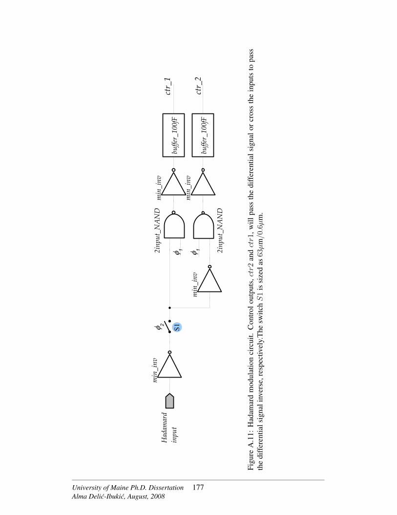
Figu
reA
.11:
Had
amar
dm
odul
atio
nci
rcui
t.C
ontr
olou
tput
s,ctr2
andctr1
,will
pass
the
diff
eren
tials
igna
lor
cros
sth
ein
puts
topa
ssth
edi
ffer
entia
lsig
nali
nver
se,r
espe
ctiv
ely.
The
switc
hS
1is
size
das
63µ
m/0.6µ
m.
University of Maine Ph.D. DissertationAlma Delic-Ibukic, August, 2008
177

Figu
reA
.12:
Fully
diff
eren
tial
seco
nd-o
rder
∆Σ
mod
ulat
orim
plem
ente
dus
ing
switc
hed-
capa
cito
rci
rcui
ts.
Switc
hes
labe
lledS
1th
roug
hS
4ar
esi
zed
as79.2µ
m/0.6µ
m,5
2.8µ
m/0.6µ
m,1
3.2µ
m/0.6µ
m,3
9.75µ
m/0.6µ
m,r
espe
ctiv
ely.
University of Maine Ph.D. DissertationAlma Delic-Ibukic, August, 2008
178

APPENDIX B
Test Board Schematics and Layout
University of Maine Ph.D. DissertationAlma Delic-Ibukic, August, 2008
179

Figu
reB
.1:T
estb
oard
sche
mat
ics
ford
ata
capt
ure
and
FPG
Ain
terf
ace
(i.e
.Had
amar
dm
odul
atio
nse
quen
ce).
University of Maine Ph.D. DissertationAlma Delic-Ibukic, August, 2008
180

Figu
reB
.2:T
estb
oard
sche
mat
ics
fort
hesu
pply
and
refe
renc
evo
ltage
sge
nera
tion
fort
wo
chip
s.
University of Maine Ph.D. DissertationAlma Delic-Ibukic, August, 2008
181

Figu
reB
.3:T
estb
oard
sche
mat
ics
forg
ener
atio
nof
adi
ffer
entia
linp
utsi
gnal
,clo
cksi
gnal
and
FPG
Acl
ock
sign
al.
University of Maine Ph.D. DissertationAlma Delic-Ibukic, August, 2008
182
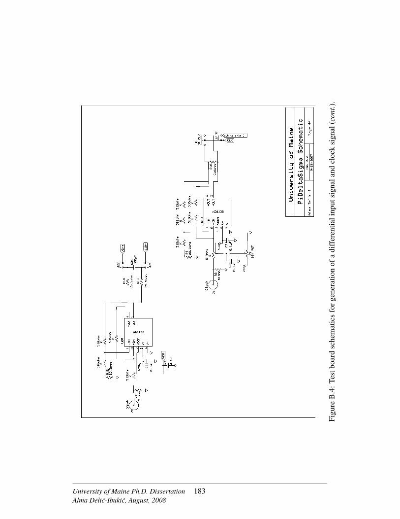
Figu
reB
.4:T
estb
oard
sche
mat
ics
forg
ener
atio
nof
adi
ffer
entia
linp
utsi
gnal
and
cloc
ksi
gnal
(con
t.).
University of Maine Ph.D. DissertationAlma Delic-Ibukic, August, 2008
183
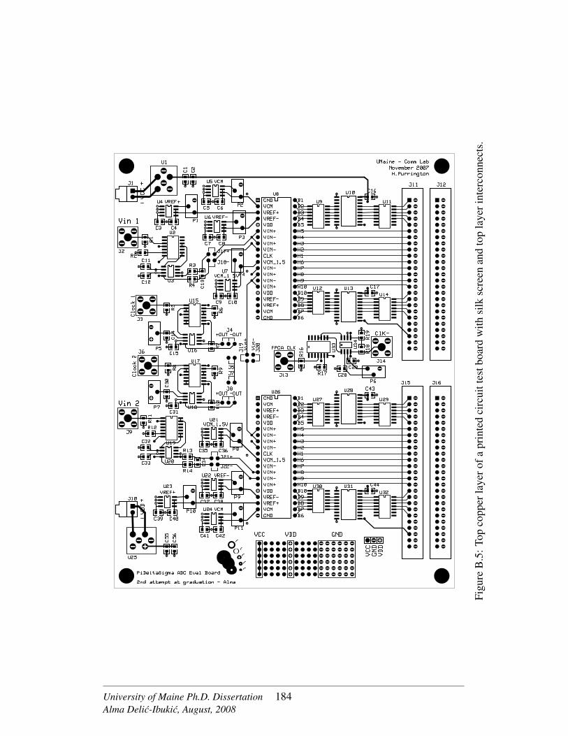
Figu
reB
.5:T
opco
pper
laye
rofa
prin
ted
circ
uitt
estb
oard
with
silk
scre
enan
dto
pla
yeri
nter
conn
ects
.
University of Maine Ph.D. DissertationAlma Delic-Ibukic, August, 2008
184
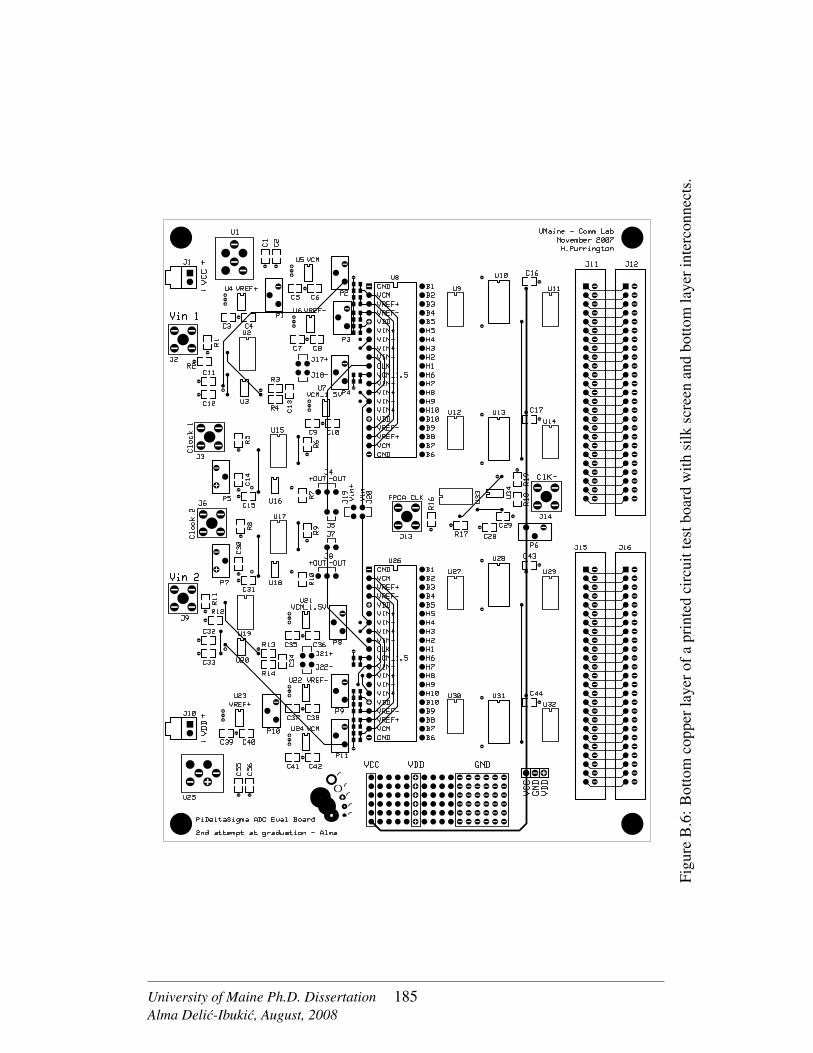
Figu
reB
.6:B
otto
mco
pper
laye
rofa
prin
ted
circ
uitt
estb
oard
with
silk
scre
enan
dbo
ttom
laye
rint
erco
nnec
ts.
University of Maine Ph.D. DissertationAlma Delic-Ibukic, August, 2008
185

Biography of the Author
Alma Delic-Ibukic was born in Bihac, Bosnia-Herzegovina. She received her
high school education from Mount Desert Island High School in Bar Harbor, Maine
graduating in 1997.
She entered the University of Maine in 1997 and obtained her Bachelor of Sci-
ence and Master of Science degrees in Electrical Engineering in 2002 and 2004, re-
spectively. During her undergraduate education, she completed a semester long Co-op
assignment at Texas Instruments Inc. (Dallas, TX) where she worked on test and char-
acterization of high-speed ADCs.
Since September 2004, she has served as a Research Assistant in the Com-
munications and Signal Processing Laboratory. Her current research interests include
mixed-signal CMOS design and real-time calibration techniques for high-speed, high-
resolution ADCs. She is a member of IEEE, Tau Beta Pi and Eta Kappa Nu.
Alma is a candidate for the Doctor of Philosophy degree in Electrical Engineer-
ing from The University of Maine in August 2008.
University of Maine Ph.D. DissertationAlma Delic-Ibukic, August, 2008
186