all-digital background calibration of a successive...
TRANSCRIPT

1
All-Digital Background Calibration of a SuccessiveApproximation ADC using the “Split ADC”
ArchitectureJohn A. McNeill, Ka Yan Chan, Michael Coln, Christopher David, and Cody Brenneman
Abstract—The “Split ADC” architecture enables fully digitalcalibration and correction of nonlinearity errors due to capacitormismatch in a Successive Approximation (SAR) ADC. The diearea of a single ADC design is split into two independenthalves, each converting the same input signal. Total area andpower is unchanged, resulting in minimal increase in analogcomplexity. For each conversion, the half-sized ADCs generatetwo independent outputs which are digitally corrected usingestimates of capacitor mismatch errors for each ADC. The ADCoutputs are averaged to produce the ADC output code. Thedifference of the two outputs is used in a background calibrationalgorithm which estimates the error in the correction parameters.Any nonzero difference drives an LMS feedback loop toward zerodifference which can only occur when the average error in eachcorrection parameter is zero. Simulation of a 16 bit 1Msps SARADC show calibration convergence within 200 000 samples.
Index Terms: Analog-digital conversion, adaptive systems, cal-ibration, self-calibrating, digital background calibration, mixedanalog-digital integrated circuits.
I. INTRODUCTION
THE successive approximation (SAR) architecture contin-ues to be of interest for Nyquist rate analog-to-digital
converters (ADCs) in nanoscale CMOS [1]. In particular,the charge-balance SAR ADC [2] is well suited to CMOSintegration and offers a good compromise in the tradeoffsamong sampling rate, power, dynamic range, and die area.For the charge-balance SAR, ADC linearity is limited bycapacitor matching. As CMOS devices enter the nanoscaleregion, difficulty with matching in the presence of increasedvariability becomes more critical [3], necessitating some formof calibration. Since scaling of CMOS device dimensionsoffers clear advantages for digital circuitry in terms of den-sity, speed, and integration, it becomes advantageous to pushcalibration into the digital domain if possible.
This paper presents an application of the “Split ADC” [4],[5] architecture to the problem of calibrating and correctinglinearity errors in successive approximation ADCs. Comparedwith the work in [5], the novel content in this paper is theextension of the split ADC concept to the SAR architecture.
This paper is organized as follows: Section II reviews issuesassociated with errors in successive approximation ADCs, aswell as analog and digital methods of correcting errors. SectionIII describes the novel aspects of the hardware design of thesplit SAR ADC. Section IV describes the error correction andcalibration process using the split ADC architecture. SectionV describes the design of a 16b 1MSps SAR ADC in a 180nm
CMOS process, with simulation results at the behavioral andextracted silicon levels.
II. SAR ADC REVIEW
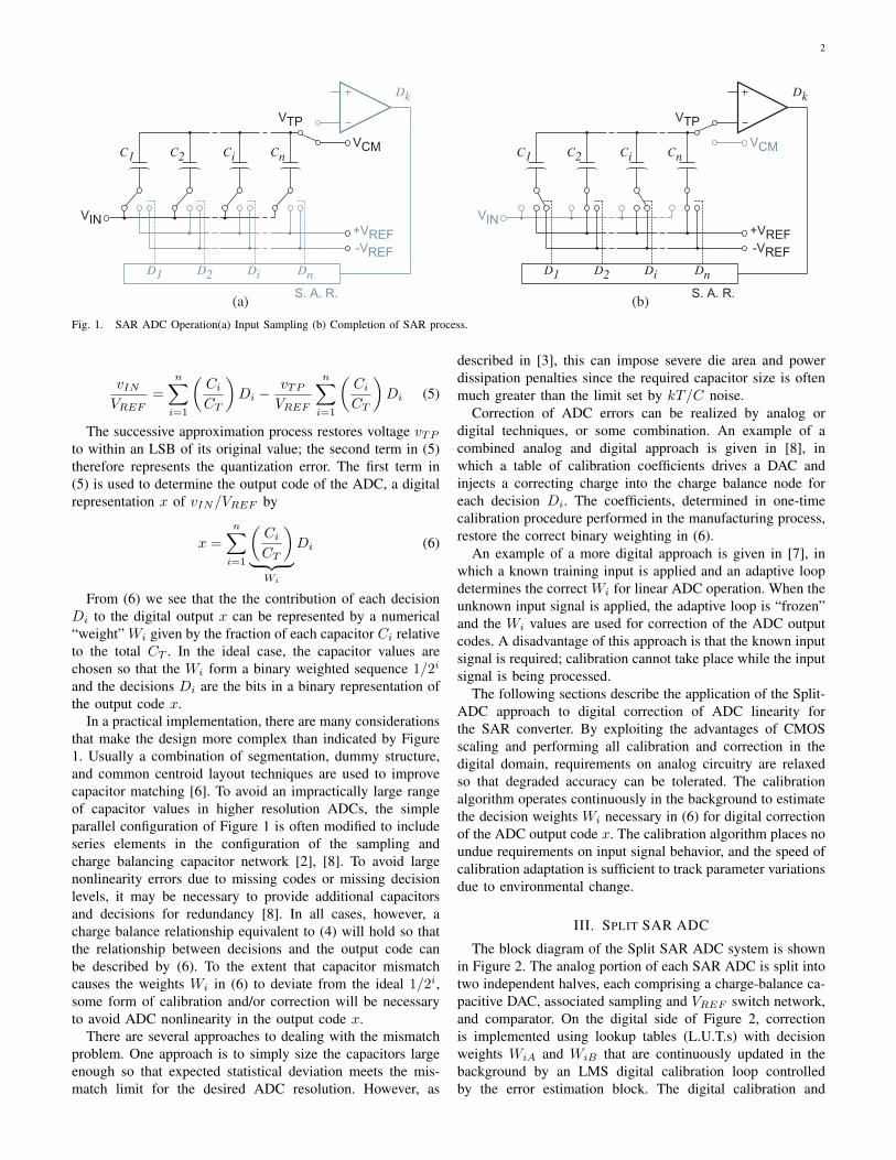
Figure 1 shows a simplified version of charge-balance SARADC operation [6]. For simplicity only half of a differentialimplementation is shown; all results are applicable to thefully differential case. Also for simplicity, we will temporarilyignore offset error; the effect of offset will be discussed inSection IV-B. In the sample phase shown in Fig. 1a, the inputsignal vIN is sampled on the bottom plates of all capacitors.The top plate voltage VTP is sampled to VCM , the desiredcommon-mode voltage at the comparator input. Assuming forsimplicity VCM = 0 (VCM cancels in a fully differentialimplementation), the charge on each capacitor is given by
Qi = CivIN (1)
and the total charge QT on all capacitors is
QT =n∑
i=1
CivIN = CT vIN with CT =n∑
i=1
Ci (2)
with CT the total capacitance.In the successive approximation process shown in figure
1b, the capacitor top plates are applied to the input of thecomparator and the bottom plates are switched to referencevoltages ±VREF in accordance with the comparator decisionsDk = ±1, where Dk is the decision in the kth approximationcycle which is stored in the successive approximation register(S.A.R.). Since the comparator input ideally draws no current,the total charge on the capacitor top plates will remainconstant. At the conclusion of the successive approximationprocess, the total charge on the capacitors is given by
QT =n∑
i=1
Ci(DiVREF − vTP ) (3)
where vTP is the voltage at the comparator input. By chargeconservation we equate (3) and (2) to obtain
CT vIN =n∑
i=1
Ci(DiVREF − vTP ) (4)
Rearranging (4) and solving for vIN/VREF gives
2
N DELAY STAGES
MN1
MN3
MP4
MP2
VDD
VCTL(P)
VCTL
VCTL(N)
Td
VCM
VTP
S. A. R.
CL
Cn
vOvI
CiC2C1
DnDiD2D1
Dk
CnCiC2C1
DnDiD2D1
VIN+VREF-VREF
VCM
VTP
S. A. R.
CnCiC2C1
Dn
(a) (b)
DiD2D1
Dk
VIN+VREF-VREF
Fig. 1. SAR ADC Operation(a) Input Sampling (b) Completion of SAR process.
vIN
VREF=
n∑i=1
(Ci
CT
)Di −
vTP
VREF
n∑i=1
(Ci
CT
)Di (5)
The successive approximation process restores voltage vTP
to within an LSB of its original value; the second term in (5)therefore represents the quantization error. The first term in(5) is used to determine the output code of the ADC, a digitalrepresentation x of vIN/VREF by
x =n∑
i=1
(Ci
CT
)︸ ︷︷ ︸
Wi
Di (6)
From (6) we see that the the contribution of each decisionDi to the digital output x can be represented by a numerical“weight” Wi given by the fraction of each capacitor Ci relativeto the total CT . In the ideal case, the capacitor values arechosen so that the Wi form a binary weighted sequence 1/2i
and the decisions Di are the bits in a binary representation ofthe output code x.
In a practical implementation, there are many considerationsthat make the design more complex than indicated by Figure1. Usually a combination of segmentation, dummy structure,and common centroid layout techniques are used to improvecapacitor matching [6]. To avoid an impractically large rangeof capacitor values in higher resolution ADCs, the simpleparallel configuration of Figure 1 is often modified to includeseries elements in the configuration of the sampling andcharge balancing capacitor network [2], [8]. To avoid largenonlinearity errors due to missing codes or missing decisionlevels, it may be necessary to provide additional capacitorsand decisions for redundancy [8]. In all cases, however, acharge balance relationship equivalent to (4) will hold so thatthe relationship between decisions and the output code canbe described by (6). To the extent that capacitor mismatchcauses the weights Wi in (6) to deviate from the ideal 1/2i,some form of calibration and/or correction will be necessaryto avoid ADC nonlinearity in the output code x.
There are several approaches to dealing with the mismatchproblem. One approach is to simply size the capacitors largeenough so that expected statistical deviation meets the mis-match limit for the desired ADC resolution. However, as
described in [3], this can impose severe die area and powerdissipation penalties since the required capacitor size is oftenmuch greater than the limit set by kT/C noise.
Correction of ADC errors can be realized by analog ordigital techniques, or some combination. An example of acombined analog and digital approach is given in [8], inwhich a table of calibration coefficients drives a DAC andinjects a correcting charge into the charge balance node foreach decision Di. The coefficients, determined in one-timecalibration procedure performed in the manufacturing process,restore the correct binary weighting in (6).
An example of a more digital approach is given in [7], inwhich a known training input is applied and an adaptive loopdetermines the correct Wi for linear ADC operation. When theunknown input signal is applied, the adaptive loop is “frozen”and the Wi values are used for correction of the ADC outputcodes. A disadvantage of this approach is that the known inputsignal is required; calibration cannot take place while the inputsignal is being processed.
The following sections describe the application of the Split-ADC approach to digital correction of ADC linearity forthe SAR converter. By exploiting the advantages of CMOSscaling and performing all calibration and correction in thedigital domain, requirements on analog circuitry are relaxedso that degraded accuracy can be tolerated. The calibrationalgorithm operates continuously in the background to estimatethe decision weights Wi necessary in (6) for digital correctionof the ADC output code x. The calibration algorithm places noundue requirements on input signal behavior, and the speed ofcalibration adaptation is sufficient to track parameter variationsdue to environmental change.
III. SPLIT SAR ADC
The block diagram of the Split SAR ADC system is shownin Figure 2. The analog portion of each SAR ADC is split intotwo independent halves, each comprising a charge-balance ca-pacitive DAC, associated sampling and VREF switch network,and comparator. On the digital side of Figure 2, correctionis implemented using lookup tables (L.U.T.s) with decisionweights WiA and WiB that are continuously updated in thebackground by an LMS digital calibration loop controlledby the error estimation block. The digital calibration and

3
N DELAY STAGES
MN1
MN3
MP4
MP2
VDD
VCTL(P)
VCTL
VCTL(N)
Td
VSS
CL
Cn
vOvI
CiC2C1 CnCiC2C1
DnDiD2D1
VTP
SAMPLING / ±VREF / DAC SWITCH NETWORK
S. A. R.
PREAMPS LATCH
COMPARATOR
VINP
500fF UNIT CAP 63fF UNIT CAP
ANALOG DIGITAL ERROR CORRECTION / CALIBRATION
63fF UNIT CAP 63fF UNIT CAP 63fF UNIT CAP
C7
Cs1
C6C5C4R
500fF 250fF 125fF 63fF
63fF C10C9C8C7R
500fF 250fF 125fF 63fF
Cs2
63fF C13C12C11C10R
500fF 250fF 125fF 63fF
Cs3
63fF C16C15C14C13R
500fF 250fF 125fF 63fF
VINM
+VREF-VREF
ERRORESTIMATION
SAMPLING / ±VREF / DAC SWITCH NETWORK
CAPACITIVE DAC
CAPACITIVE DAC
SAMPLING / ±VREF / DAC SWITCH NETWORK
SAMPLING / ±VREF / DAC SWITCH NETWORK
DkA
diA
diA
diA
diB diB
xA
Δx
S. A. R.
PRN
-
+
WiA
Σ
Σ μ
x+
+
ˆ ε iA
PRN WiB Σ μˆ ε iB
PREAMPS LATCH
DECISIONWEIGHTL.U.T.s
SEGMENTASSIGNMENT
LOGIC
COMPARATOR
DkB diB xBΣ
Fig. 2. Split SAR ADC Block Diagram.
correction are discussed in more detail in Section IV; theremainder of this section describes the analog circuitry.
A. Capacitive DAC
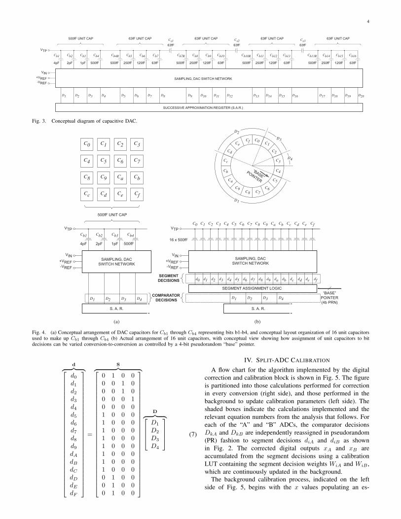
In the example implementation shown in Figure 2, thecapacitive DAC is divided into 5 blocks each representing4 comparator decision bits. A conceptual block diagram ofthe capacitive DAC implemented in this design is shown inFig. 3. The total capacitance was determined from kT/Cnoise considerations. Bits 1-4 use 500fF unit capacitors; allremaining bits use 63fF unit capacitors. The design shown heremakes heavy use of redundancy, with redundant bits includedfor every fourth decision. This is excessively conservative andwas done to ease layout and ensure that eventual silicon couldbe calibrated, rather than to optimize area or SAR decisions.With the redundancy provided by overlap between the blocks,16-b resolution is achieved with a total of 20 comparatordecisions D1 −D20.
The following subsection describes a key novel feature ofthe hardware design: assignment of comparator decisions tocapacitor segments is not fixed, but rather can be controlledon a conversion-by-conversion basis.
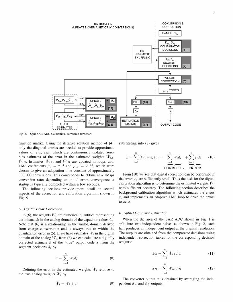
B. Dynamic Segment Assignment
Figure 4 illustrates the capacitor segment assignment pro-cess using the four MSBs of the converter as an example. Fig-ure 4a shows the standard SAR function, with binary weightedcapacitors Cb1 − Cb4 switched to the ±VREF reference asdetermined by the comparator decisions D1 − D4 loadedinto the SAR. To improve matching, the capacitor values arerealized using a unit capacitor array. Usually the assignment ofsegment capacitor switches to comparator decisions is fixed,often in a common centroid pattern which minimizes mismatcherrors. In this work, however, the segment assignment logic(shown in Figure 4b) dynamically assigns the comparatordecisions D1 −D4 to different segments. The decisions seen
by each segment’s VREF switch are denoted by the segmentdecisions d1 − df in Figure 4b.
Operation of the segment assignment logic is shown inconceptual form in Figure 4b. As shown in the diagram,groups of capacitor segments are assigned to each comparatordecision as directed by a “base” pointer, which is varied inpseudorandom (PR) fashion on a conversion-by-conversionbasis. In the example shown, the ”base” pointer value is 5,so the first 8 segments beginning at location 5 (C5 − Cc)represent comparator decision D1. The segment assignmentlogic routes comparator decision D1 to segment decisionsd5−dc which control the switches corresponding to capacitorsegments C5 − Cc. The switches for the next 4 segments,Cd−C0, are controlled by comparator decision D2. Similarly,capacitors C1 and C2 are controlled by comparator decisionD3 and capacitor C3 is controlled by comparator decision D4.Note that there will always be one segment which is not used;this ensures that as the “base” pointer is changed there willalways be different segments used even in the case of a DCinput.
In summary, the key novel feature of the hardware design isthe calibration algorithm’s use of a segment assignment logicblock and the individually controlled segment switches to dy-namically change the assignment of comparator bit decisionsDk to capacitor segment decisions di. This feature is key tothe calibration algorithm described in section IV.
C. Matrix Representation
The operation of the segment assignment logic can berepresented in matrix form; for the example of Figure 4b, theassignment of comparator decisions Dk to segment decisionsdi is given by (7). The segment assignment matrix S indicateshow comparator decisions in D are assigned to each segmentswitch control in d .
4
N DELAY STAGES
MN1
MN3
MP4
MP2
VDD
VCTL(P)
VCTL
VCTL(N)
Td
VSS
CL
Cn
vOvI
CiC2C1 CnCiC2C1
DnDiD2D1
VTP
SAMPLING, DAC SWITCH NETWORK
Cb4Cb3Cb2Cb1
VIN
4pF 2pF 1pF 500fF
500fF UNIT CAP 63fF UNIT CAP 63fF UNIT CAP 63fF UNIT CAP 63fF UNIT CAP
Cb7
Cs1
Cb6Cb5Cb4R
500fF 250fF 125fF 63fF
63fF
Cb10Cb9Cb8Cb7R
500fF 250fF 125fF 63fF
Cs263fF
Cb13Cb12Cb11Cb10R
500fF 250fF 125fF 63fF
Cs363fF
Cb16Cb15Cb14Cb13R
D4D3D2D1 D7D6D5 D10 D11 D12D9 D14 D15 D16D13 D18 D19 D20D17D8
500fF 250fF 125fF 63fF
+VREF-VREF
SUCCESSIVE APPROXIMATION REGISTER (S.A.R.)
Fig. 3. Conceptual diagram of capacitive DAC.
N DELAY STAGES
MN1
MN3
MP4
MP2
VDD
VCTL(P)
VCTL
VCTL(N)
Td
VSS
CL
Cn
vOvI
CiC2C1 CnCiC2C1
DnDiD2D1
VTP
SAMPLING, DAC SWITCH NETWORK
COMPARATORDECISIONS
C4C3C2C1
VIN
4pF 2pF 1pF 500fF
500fF UNIT CAP 63fF UNIT CAP 63fF UNIT CAP 63fF UNIT CAP 63fF UNIT CAP
C7
Cs1
C6C5C4R
500fF 250fF 125fF 63fF
63fF C10C9C8C7R
500fF 250fF 125fF 63fF
Cs2
63fF C13C12C11C10R
500fF 250fF 125fF 63fF
Cs3
63fF C16C15C14C13R
500fF 250fF 125fF 63fF
+VREF-VREF
VTPCb4Cb3Cb2Cb1
(a) (b)
Cc
VIN
4pF 2pF 1pF 500fF
500fF UNIT CAP
D4D3D2D1
D4
+VREF-VREF
VTP
C2 C3C1C0
VIN
16 x 500fF
D4D3D2D1
+VREF-VREF
Cd Ce Cf
C8 C9 Ca Cb
C4 C5 C6 C7
Cc Cd Ce CfC8 C9 Ca CbC4 C5 C6 C7
dc dd ded8 d9 da dbd4 d5 d6 d7d2 d3d1d0 df
C0 C1 C2 C3
CC CD CE CF
C8 C9 CA CB
C4 C5 C6 C7
C0 C1 C2 C3
Cc
Cd
CeCf
C8C9
Ca
Cb C4
C5
C6C7
C0 C1
C2
C3
“BASE”
POINTER
D3
D2
D1
SAMPLING, DAC SWITCH NETWORK
SEGMENT ASSIGNMENT LOGIC
S. A. R. S. A. R.
“BASE”POINTER(4b PRN)
SEGMENTDECISIONS
Fig. 4. (a) Conceptual arrangement of DAC capacitors for Cb1 through Cb4 representing bits b1-b4, and conceptual layout organization of 16 unit capacitorsused to make up Cb1 through Cb4 (b) Actual arrangement of 16 unit capacitors, with conceptual view showing how assignment of unit capacitors to bitdecisions can be varied conversion-to-conversion as controlled by a 4-bit pseudorandom “base” pointer.
d︷ ︸︸ ︷
d0
d1
d2
d3
d4
d5
d6
d7
d8
d9
dA
dB
dC
dD
dE
dF
=
S︷ ︸︸ ︷
0 1 0 00 0 1 00 0 1 00 0 0 10 0 0 01 0 0 01 0 0 01 0 0 01 0 0 01 0 0 01 0 0 01 0 0 01 0 0 00 1 0 00 1 0 00 1 0 0
D︷ ︸︸ ︷D1
D2
D3
D4
(7)
IV. SPLIT-ADC CALIBRATION
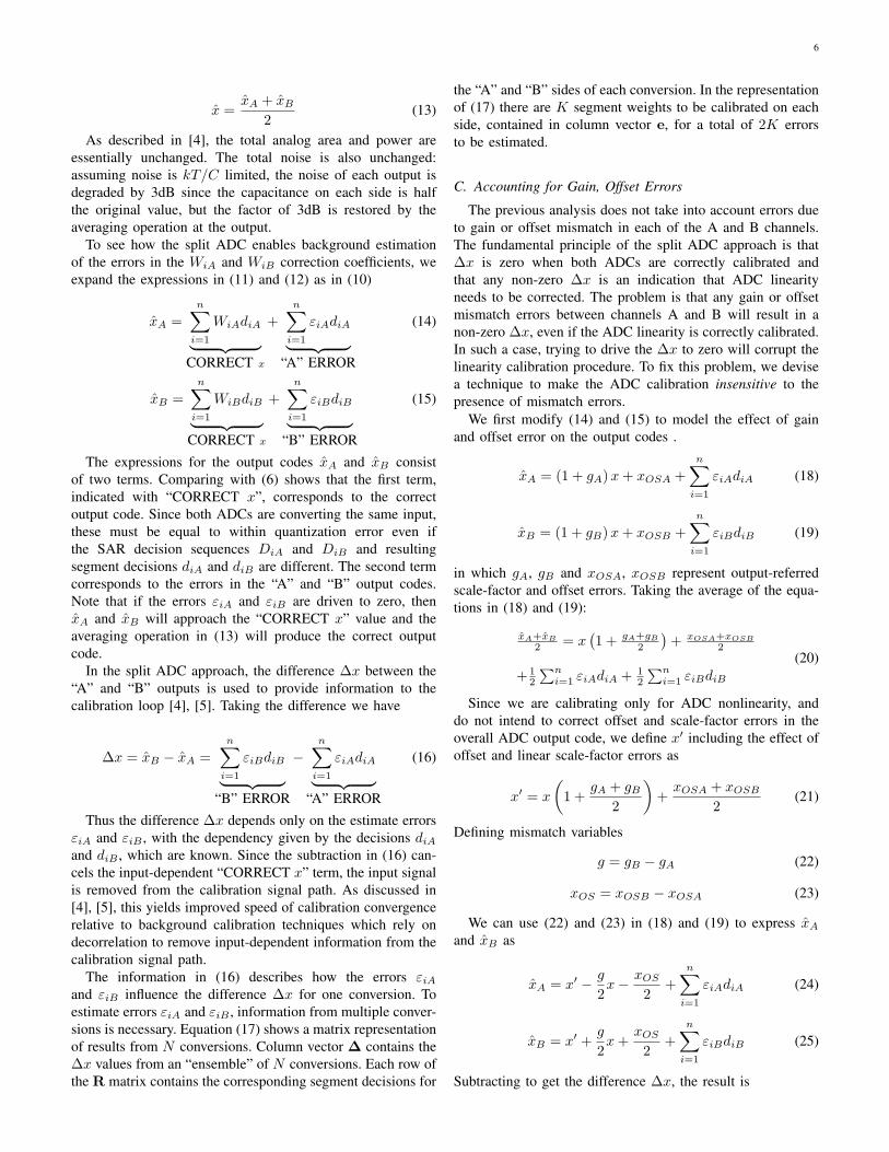
A flow chart for the algorithm implemented by the digitalcorrection and calibration block is shown in Fig. 5. The figureis partitioned into those calculations performed for correctionin every conversion (right side), and those performed in thebackground to update calibration parameters (left side). Theshaded boxes indicate the calculations implemented and therelevant equation numbers from the analysis that follows. Foreach of the “A” and “B” ADCs, the comparator decisionsDkA and DkB are independently reassigned in pseudorandom(PR) fashion to segment decisions diA and diB as shownin Fig. 2. The corrected digital outputs xA and xB areaccumulated from the segment decisions using a calibrationLUT containing the segment decision weights WiA and WiB ,which are continuously updated in the background.
The background calibration process, indicated on the leftside of Fig. 5, begins with the x values populating an es-
5
Fig. 5. Split SAR ADC Calibration, correction flowchart
timation matrix. Using the iterative solution method of [4],only the diagonal entries are needed to provide approximatevalues of εiA, εiB , which are continuously updated zero-bias estimates of the error in the estimated weights WiA,WiB . Estimates WiA, and WiB are updated in loops withLMS coefficients µe = 2−4 and µW = 2−13, which werechosen to give an adaptation time constant of approximately300 000 conversions. This corresponds to 300ms at a 1Mspsconversion rate; depending on initial error, convergence atstartup is typically completed within a few seconds.
The following sections provide more detail on severalaspects of the correction and calibration algorithm shown inFig. 5.
A. Digital Error Correction
In (6), the weights Wi are numerical quantities representingthe mismatch in the analog domain of the capacitor values Ci.Note that (6) is a relationship in the analog domain derivedfrom charge conservation and is always true to within thequantization error in (5). If we have estimates Wi in the digitaldomain of the analog Wi, from (6) we can calculate a digitallycorrected estimate x of the “true” output code x from thesegment decisions di by
x =n∑
i=1
Widi (8)
Defining the error in the estimated weights Wi relative tothe true analog weights Wi by
Wi = Wi + εi (9)
substituting into (8) gives
x =n∑
i=1
(Wi + εi) di =n∑
i=1
Widi︸ ︷︷ ︸CORRECT x
+n∑
i=1
εidi︸ ︷︷ ︸ERROR
(10)
From (10) we see that digital correction can be performed ifthe errors εi are sufficiently small. Thus the task for the digitalcalibration algorithm is to determine the estimated weights Wi
with sufficient accuracy. The following section describes thebackground calibration algorithm which estimates the errorsεi and implements an adaptive LMS loop to drive the errorsto zero.
B. Split-ADC Error Estimation
When the die area of the SAR ADC shown in Fig. 1 issplit into two independent halves as shown in Fig. 2, eachhalf produces an independent output at the original resolution.The outputs are obtained from the comparator decisions usingindependent correction tables for the corresponding decisionweights:
xA =n∑
i=1
WiAdiA (11)
xB =n∑
i=1
WiBdiB (12)
The converter output x is obtained by averaging the inde-pendent xA and xB outputs:
6
x =xA + xB
2(13)
As described in [4], the total analog area and power areessentially unchanged. The total noise is also unchanged:assuming noise is kT/C limited, the noise of each output isdegraded by 3dB since the capacitance on each side is halfthe original value, but the factor of 3dB is restored by theaveraging operation at the output.
To see how the split ADC enables background estimationof the errors in the WiA and WiB correction coefficients, weexpand the expressions in (11) and (12) as in (10)
xA =n∑
i=1
WiAdiA︸ ︷︷ ︸CORRECT x
+n∑
i=1
εiAdiA︸ ︷︷ ︸“A” ERROR
(14)
xB =n∑
i=1
WiBdiB︸ ︷︷ ︸CORRECT x
+n∑
i=1
εiBdiB︸ ︷︷ ︸“B” ERROR
(15)
The expressions for the output codes xA and xB consistof two terms. Comparing with (6) shows that the first term,indicated with “CORRECT x”, corresponds to the correctoutput code. Since both ADCs are converting the same input,these must be equal to within quantization error even ifthe SAR decision sequences DiA and DiB and resultingsegment decisions diA and diB are different. The second termcorresponds to the errors in the “A” and “B” output codes.Note that if the errors εiA and εiB are driven to zero, thenxA and xB will approach the “CORRECT x” value and theaveraging operation in (13) will produce the correct outputcode.
In the split ADC approach, the difference ∆x between the“A” and “B” outputs is used to provide information to thecalibration loop [4], [5]. Taking the difference we have
∆x = xB − xA =n∑
i=1
εiBdiB︸ ︷︷ ︸“B” ERROR
−n∑
i=1
εiAdiA︸ ︷︷ ︸“A” ERROR
(16)
Thus the difference ∆x depends only on the estimate errorsεiA and εiB , with the dependency given by the decisions diA
and diB , which are known. Since the subtraction in (16) can-cels the input-dependent “CORRECT x” term, the input signalis removed from the calibration signal path. As discussed in[4], [5], this yields improved speed of calibration convergencerelative to background calibration techniques which rely ondecorrelation to remove input-dependent information from thecalibration signal path.
The information in (16) describes how the errors εiA
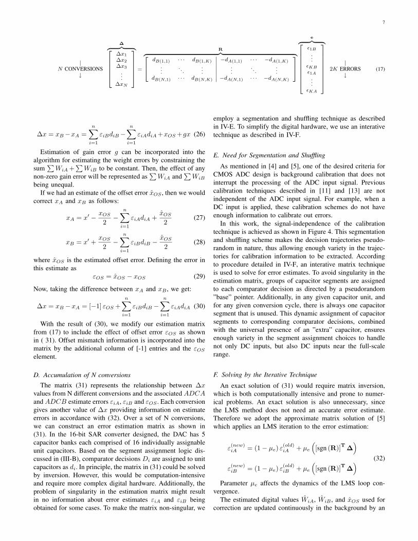
and εiB influence the difference ∆x for one conversion. Toestimate errors εiA and εiB , information from multiple conver-sions is necessary. Equation (17) shows a matrix representationof results from N conversions. Column vector ∆ contains the∆x values from an “ensemble” of N conversions. Each row ofthe R matrix contains the corresponding segment decisions for
the “A” and “B” sides of each conversion. In the representationof (17) there are K segment weights to be calibrated on eachside, contained in column vector e, for a total of 2K errorsto be estimated.
C. Accounting for Gain, Offset Errors
The previous analysis does not take into account errors dueto gain or offset mismatch in each of the A and B channels.The fundamental principle of the split ADC approach is that∆x is zero when both ADCs are correctly calibrated andthat any non-zero ∆x is an indication that ADC linearityneeds to be corrected. The problem is that any gain or offsetmismatch errors between channels A and B will result in anon-zero ∆x, even if the ADC linearity is correctly calibrated.In such a case, trying to drive the ∆x to zero will corrupt thelinearity calibration procedure. To fix this problem, we devisea technique to make the ADC calibration insensitive to thepresence of mismatch errors.
We first modify (14) and (15) to model the effect of gainand offset error on the output codes .
xA = (1 + gA)x+ xOSA +n∑
i=1
εiAdiA (18)
xB = (1 + gB)x+ xOSB +n∑
i=1
εiBdiB (19)
in which gA, gB and xOSA, xOSB represent output-referredscale-factor and offset errors. Taking the average of the equa-tions in (18) and (19):
xA+xB
2 = x(1 + gA+gB
2
)+ xOSA+xOSB
2
+ 12
∑ni=1 εiAdiA + 1
2
∑ni=1 εiBdiB
(20)
Since we are calibrating only for ADC nonlinearity, anddo not intend to correct offset and scale-factor errors in theoverall ADC output code, we define x′ including the effect ofoffset and linear scale-factor errors as
x′ = x
(1 +
gA + gB
2
)+xOSA + xOSB
2(21)
Defining mismatch variables
g = gB − gA (22)
xOS = xOSB − xOSA (23)
We can use (22) and (23) in (18) and (19) to express xA
and xB as
xA = x′ − g
2x− xOS
2+
n∑i=1
εiAdiA (24)
xB = x′ +g
2x+
xOS
2+
n∑i=1
εiBdiB (25)
Subtracting to get the difference ∆x, the result is
7
|N CONVERSIONS
↓
∆︷ ︸︸ ︷∆x1
∆x2
∆x3
...∆xN
=
R︷ ︸︸ ︷ dB(1,1) · · · dB(1,K) −dA(1,1) · · · −dA(1,K)
.... . .
......
. . ....
dB(N,1) · · · dB(N,K) −dA(N,1) · · · −dA(N,K)
e︷ ︸︸ ︷
ε1B
...εKB
ε1A
...εKA
|
2K ERRORS↓
(17)
∆x = xB−xA =n∑
i=1
εiBdiB−n∑
i=1
εiAdiA +xOS +gx (26)
Estimation of gain error g can be incorporated into thealgorithm for estimating the weight errors by constraining thesum
∑WiA +
∑WiB to be constant. Then, the effect of any
non-zero gain error will be represented as∑WiA and
∑WiB
being unequal.If we had an estimate of the offset error xOS , then we would
correct xA and xB as follows:
xA = x′ − xOS
2−
n∑i=1
εiAdiA +xOS
2(27)
xB = x′ +xOS
2−
n∑i=1
εiBdiB − xOS
2(28)
where xOS is the estimated offset error. Defining the error inthis estimate as
εOS = xOS − xOS (29)
Now, taking the difference between xA and xB , we get:
∆x = xB −xA = [−1] εOS +n∑
i=1
εiBdiB −n∑
i=1
εiAdiA (30)
With the result of (30), we modify our estimation matrixfrom (17) to include the effect of offset error εOS as shownin ( 31). Offset mismatch information is incorporated into thematrix by the additional column of [-1] entries and the εOS
element.
D. Accumulation of N conversions
The matrix (31) represents the relationship between ∆xvalues from N different conversions and the associated ADCAand ADCB estimate errors εiA, εiB and εOS . Each conversiongives another value of ∆x providing information on estimateerrors in accordance with (32). Over a set of N conversions,we can construct an error estimation matrix as shown in(31). In the 16-bit SAR converter designed, the DAC has 5capacitor banks each comprised of 16 individually assignableunit capacitors. Based on the segment assignment logic dis-cussed in (III-B), comparator decisions Di are assigned to unitcapacitors as di. In principle, the matrix in (31) could be solvedby inversion. However, this would be computation-intensiveand require more complex digital hardware. Additionally, theproblem of singularity in the estimation matrix might resultin no information about error estimates εiA and εiB beingobtained for some cases. To make the matrix non-singular, we
employ a segmentation and shuffling technique as describedin IV-E. To simplify the digital hardware, we use an interativetechnique as described in IV-F.
E. Need for Segmentation and Shuffling
As mentioned in [4] and [5], one of the desired criteria forCMOS ADC design is background calibration that does notinterrupt the processing of the ADC input signal. Previouscalibration techniques described in [11] and [13] are notindependent of the ADC input signal. For example, when aDC input is applied, these calibration schemes do not haveenough information to calibrate out errors.
In this work, the signal-independence of the calibrationtechnique is achieved as shown in Figure 4. This segmentationand shuffling scheme makes the decision trajectories pseudo-random in nature, thus allowing enough variety in the trajec-tories for calibration information to be extracted. Accordingto procedure detailed in IV-F, an interative matrix techniqueis used to solve for error estimates. To avoid singularity in theestimation matrix, groups of capacitor segments are assignedto each comparator decision as directed by a pseudorandom”base” pointer. Additionally, in any given capacitor unit, andfor any given conversion cycle, there is always one capacitorsegment that is unused. This dynamic assignment of capacitorsegments to corresponding comparator decisions, combinedwith the universal presence of an ”extra” capacitor, ensuresenough variety in the segment assignment choices to handlenot only DC inputs, but also DC inputs near the full-scalerange.
F. Solving by the Iterative Technique
An exact solution of (31) would require matrix inversion,which is both computationally intensive and prone to numer-ical problems. An exact solution is also unnecessary, sincethe LMS method does not need an accurate error estimate.Therefore we adopt the approximate matrix solution of [5]which applies an LMS iteration to the error estimation:
ε(new)iA = (1− µe) ε(old)
iA + µe
([sgn (R)]T ∆
)ε(new)iB = (1− µe) ε(old)
iB + µe
([sgn (R)]T ∆
) (32)
Parameter µe affects the dynamics of the LMS loop con-vergence.
The estimated digital values WiA, WiB , and xOS used forcorrection are updated continuously in the background by an

8
|N CONVERSIONS
↓
∆︷ ︸︸ ︷∆x1
∆x2
∆x3
...∆xN
=
R︷ ︸︸ ︷ dB(1,1) · · · dB(1,K) −dA(1,1) · · · −dA(1,K) −1
.... . .
......
. . ....
...dB(N,1) · · · dB(N,K) −dA(N,1) · · · −dA(N,K) −1
e︷ ︸︸ ︷
ε1B
...εKB
ε1A
...εKA
εOS
|
2K + 1 ERRORS↓
(31)
LMS feedback loop.
W(new)iA = W
(old)iA − µW εiA
W(new)iB = W
(old)iB − µW εiB
x(new)OS = x
(old)OS − µW εOS
(33)
The LMS loop uses εOS , εiA, and εiB , which are estimatederrors in the xOS , WiA, and WiB values. The LMS multiplerµW controls the dynamics of the loop convergence. A keyadvantage of the LMS approach is that the εOS , εiA, andεiB need not be accurate; all that is required is that theybe zero-bias and (on average) steer the convergence of (33)in the correct direction. The general LMS technique is wellestablished [9], [11], [12]; the novel contributions of thiswork are in the use of the ”Split ADC” approach to extractcalibration information in the background.
By constraining∑WiA +
∑WiB = constant, we incorpo-
rate gain error calibration into the calibration of the decisionweights. The effect of applying this contraint is that any non-zero gain error in the ADC results in
∑WiA and
∑WiB
being unequal. In this work, the contraint is applied in aninterative fashion by keeping track of the change in weightsums
∑WiA and
∑WiB as shown in (34). This change in
the sum of the weights is expressed as a scalar ratio h asshown in (35). This scalar is then used to modify the weightsW
(new)iA and W (new)
iB in (33) to obtain new weights W (new)′
as shown in (36).
∑W
(old)iA +
∑W
(old)iB = A(old)
∑W
(new)iA +
∑W
(new)iB = A(new)
(34)
A(old)
A(new)= h (35)
W(new)′
iA = h.W(new)iA
W(new)′
iB = h.W(new)iB
(36)
Applying this constraint on the weights forces the gain errorof the ADC to manifest only as
∑WiA and
∑WiB being
unequal. The implementation of this contraint is representedin the overall algorithm as shown in Fig 5. It involves anadditional update of the state estimates W (new)
iA and W(new)iB
based on the current value of scalar h.
Table 1. Behavioral Simulation Parameters.PARAMETER VALUE
ADC Resolution 16bConversion Speed 1 MSps
Comparator SAR Decisions 20Input Referred Noise -96 dBFS
DAC Capacitance Total 16pFMinimum Unit 50 fFInput Referred Mismatch 50ppm
LMS Parameter µW 2−13
µe 2−4
Internal Digital Precision 24b
V. RESULTS
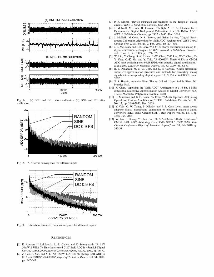
A 16-bit 1 Msps SAR converter was designed in a 0.25µmprocess, with capacitive DAC segmentation and shuffling toimplement the algorithm described above [10]. The layoutwas extracted to a combination SPICE and HDL model to betested with a MATLAB simulation of the calibration algorithm.Simulation parameters are shown in Table 1.
Figures 6a and 6b show plots of DNL and INL (in LSB)before calibration. Once the LMS calibration loop has con-verged to its steady state, the simulated linearity is better than±1LSB. Figure 7 shows ADC error in dB relative to full scale(dBFS) plotted as a function of conversion for different inputsignals: random, sinusoidal, and DC equal to 0.9 of full scale(FS). In all cases, performance within 200 000 conversions.Figure 8 show the convergence of the maximum estimationparameter error for different input signals. In all cases, theerror is below the limit required for proper ADC operationwithin 200 000 conversions. In similar fashion to [5], theultimate limit on estimation parameter error is determined byeither the internal digital precision or the value of the LMSparameters.
VI. CONCLUSION
A successive approximation ADC using the split ADCarchitecture has been presented. DNL and INL errors due tocapacitor mismatch are digitally corrected and calibration isperformed continuously in the background with a fully digitalimplementation. Behavioral simulation of a 16b 1Msps ADCshows calibration convergence within 200 000 samples.
ACKNOWLEDGMENT
This material is based upon work supported by AnalogDevices and by the National Science Foundation under GrantNo. 0523996. The authors thank the members of the Preci-sion Nyquist Converter and High-Speed Converter groups atAnalog Devices.
9
Fig. 6. (a) DNL and INL before calibration (b) DNL and INL aftercalibration.
RANDOMSINEDC 0.9 FS
Fig. 7. ADC error convergence for different inputs
RANDOMSINEDC 0.9 FS
Fig. 8. Estimation parameter error convergence for different inputs
REFERENCES
[1] E. Alpman, H. Lakdawala, L. R. Carley, and K. Soumyanath, “A 1.1V50mW 2.5GS/s 7b Time-Interleaved C-2C SAR ADC in 45nm LP DigitalCMOS,” ISSCC2009 Digest of Technical Papers, vol. 52, 2009, pp. 76-77.
[2] Z. Cao, S. Yan, and Y. Li, “A 32mW 1.25GS/s 6b 2b/step SAR ADC in0.13 µm CMOS,” ISSCC2008 Digest of Technical Papers, vol. 51, 2008,pp. 542-543.
[3] P. R. Kinget, “Device mismatch and tradeoffs in the design of analogcircuits,”IEEE J. Solid-State Circuits, June 2005.
[4] J. McNeill, M. Coln, B. Larivee, ”’A Split-ADC’ Architecture for aDeterministic Digital Background Calibration of a 16b 1MS/s ADC,”IEEE J. Solid-State Circuits, pp. 2437 - 2445, Dec. 2005.
[5] J. McNeill, M Coln, D. R. Brown, and Brian Larivee, ”Digital Back-ground Calibration Algorithm for ’Split ADC’ Architecture,” IEEE Trans.Circuits Syst. I, vol. 56, no. 2, Feb. 2009, pp. 294-306.
[6] J. L. McCreary and P. R. Gray, “All-MOS charge redistribution analog-to-digital conversion techniques. I,” IEEE Journal of Solid-State Circuits,”vol. 10 no. 6, Dec 1975, pp. 371- 379
[7] W. Liu, Y. Chang, S.-K. Hsien, B.-W. Chen, Y.-P. Lee, W.-T. Chen, T.-Y. Yang, G.-K. Ma, and Y. Chiu, ”A 600MS/s 30mW 0.13µm CMOSADC array achieving over 60dB SFDR with adaptive digital equalization,”ISSCC2009 Digest of Technical Papers, vol. 52, 2009, pp. 82-83.
[8] B. E. Amazeen, M. C. W. Coln, and G. R. Carreau, ”Quasi-differentialsuccessive-approximation structures and methods for converting analogsignals into corresponding digital signals.” U.S. Patent 6,400,302, June,2002.
[9] S. S. Haykin, Adaptive Filter Theory, 3rd ed. Upper Saddle River, NJ:Prentice Hall.
[10] K. Chan, “Applying the ”Split-ADC” Architecture to a 16 bit, 1 MS/sdifferential Successive Approximation Analog-to-Digital Converter,” M.S.Thesis, Worcester Polytechnic Institute, 2008.
[11] B. Murmann and B. E. Boser, ”A 12-bit 75-MS/s Pipelined ADC usingOpen-Loop Residue Amplification,” IEEE J. Solid-State Circuits, Vol. 38,No. 12, pp. 2040-2050, Dec. 2003.
[12] Y. Chiu, C. W. Tsang, B. Nikolic, and P. R. Gray, Least mean squareadaptive digital background calibration of pipelined analog-to-digitalconverters, IEEE Trans. Circuits Syst. I, Reg. Papers, vol. 51, no. 1, pp.3846, Jan. 2004.
[13] W. Liu, P. Huang, Y. Chiu, ”A 12b 22.5/45MS/s 3.0mW 0.059mm2
CMOS SAR ADC Achieving Over 90dB SFDR,” IEEE Solid StateCircuits Conference Digest of Technical Papers,” vol. 53, Feb 2010 pp.380-381