development and verification of soft ip core of usb 3.0 in verilog hdl baig - be thesis.pdf ·...
TRANSCRIPT

Development and Verification of Soft IP Core of USB 3.0 in Verilog HDL
B.E. (EL) PROJECT REPORT
Prepared by:
Hasan Baig
Project Advisors:
Mr. Muhammad Nauman (Internal Advisor) Mr. Fasahat Hussain (External Advisor)
Department of Electronics Engineering
N.E.D. University of Engineering and Technology Karachi-75270

Development and Verification of Soft IP Core of USB 3.0 in Verilog HDL
B.E. (EL) PROJECT REPORT
Prepared by:
Muhammad Obaid Khalid (EL-025) Hasan Baig (EL-034)
Syed Taha Munir (EL-048) Muhammad Asrar Alam (EL-068)
Project Advisors:
Mr. Muhammad Nauman (Internal Advisor) Mr. Fasahat Hussain (External Advisor)
Department of Electronics Engineering
N.E.D. University of Engineering and Technology Karachi-75270

Abstract The Universal Serial Bus (USB) is a new way of attaching devices to personal
computers. The bus architecture features two-way communication and has been
developed as a response to devices becoming smarter and requiring more
interaction with the host. USB support is included in all current PC chipsets and is
therefore available in all recently built PCs. USB, as a protocol, has also been
picked up for many non-traditional applications such as industrial automation and
control.
Universal serial bus has supported a wide variety of devices from keyboard,
mouse, flash memory device, game peripheral, imaging up to high speed broad
band devices. In addition, user applications demand a higher performance
connection between the PC and other increasingly sophisticated peripherals. USB
3.0 addresses this need by adding even faster transfer rates. It promises a data
transfer rate of 4.8 Gbps as compared to its predecessor interface USB 2.0 which
has a raw data rate at 480Mbps.
This implementation of SuperSpeed USB Memory Device, with a pipelining
concept of processing the packets, is proposed to support high speed transfer rate
and high throughputs. Alongside, the use of efficient handshaking signals complies
with optimum performance of the overall device. This implementation meets all
the required specifications with high reliability.

Acknowledgments ]
We would first of all thank ALLAH Almighty Who enabled us to carry out this project
with full devotion and consistency. It was only because of His blessings that we could
find our way up to the completion of this task. Next we would like to pay our regards to
Mr. Khursheed Hassan, the CEO of Eonsil LLC. Texas, U.S.A, for allowing us an
opportunity to work on a project revealing the cutting edge technology of USB 3.0 that
brought us up to date with the latest technology and gained us unrivalled experience in
the field of digital designing and FPGA. Along with this we would like to present our
gratitude to Mr. Fasahat Hussain of Digitech Karachi, Pakistan, for guiding us and
leading us out of trouble at each and every pinnacle of this project work. Mr. Fasahat
coordinated with us at each and every aspect and steered us into the very details.
We would also of course like to thank our internal Mr. Muhammad Nauman for co-
operating with us throughout the course of this project and co-coordinating from time
to time with Mr. Fasahat and Mr. Khursheed about our progress and problems.
In the last but not the least we would like to acknowledge the efforts of our group
members who worked tirelessly for the accomplishment of this project leading it in
parallel with our studies and other co-curricular activities. This project was not an
achievement of any individual but its credits and acknowledgements are deserved by all
hands and minds that contributed devotedly towards its triumph.
Table of Contents 1. The Implemented Architecture of USB 3.0 Memory Device .................................. 1
1.1 Architecture’s Overview.................................................................................... 1 1.2 Dual Simplex Requirement Of USB 3.0 SuperSpeed Protocols ....................... 3 1.3 PHY Chip Behavioral Model ............................................................................ 3 1.4 The Pipe Line Operation ................................................................................... 3
2. The Physical Layer Controller .................................................................................. 4
2.1 Physical Layer Overview .................................................................................. 5 2.2 USB Physical Layer .......................................................................................... 6 2.3 MAC – PHY Interface....................................................................................... 7
2.3.1 MAC – PHY Interface Signals .................................................................... 9 2.3.2 MAC – LTSSM Interface Signals ............................................................. 10 2.3.3 MAC – Link Layer Controller Interface Signals....................................... 11 2.3.4 MAC – Master Controller interface signals .............................................. 11
2.4 MAC Layer intermediate signals..................................................................... 12 2.5 Algorithmic States Machine Description of Phy Encoder .............................. 13 2.6 Algorithmic States Machine Description of Phy Decoder .............................. 16
3. The Link Layer ......................................................................................................... 18
3.1 Link Layer Overview....................................................................................... 19 3.2 Hardware Implementation of Link Layer........................................................ 19
3.2.1 Packet Disassembler .................................................................................. 20 3.2.2 Packet Assembler ...................................................................................... 20
3.3 Buffer controllers (buffer interfaces)............................................................... 21 3.4 Link Layer Controller...................................................................................... 21
3.4.1 Link Commands ........................................................................................ 21 3.4.2 Header Packet Exchange Control .............................................................. 23
3.4.2.1 IDLE STATE.............................................................................. 24 3.4.2.2 Initialization for HP integrity and flow control .......................... 25 3.4.2.3 Valid Header Packets Exchange................................................. 25 3.4.2.4 Header Packet Retry Process...................................................... 26
3.4.3 Link Power Management: ......................................................................... 27 3.4.3.1 Rules for a port to request or accept a low power link state....... 27
3.5 Error Detection Algorithm (CRC)................................................................... 27 3.5.1 Method of Parallel CRC Computation ...................................................... 28
4. The Link Training and Status State Machine ....................................................... 30
4.1 Introduction ..................................................................................................... 31 4.2 LTSSM’s Interconnections with other Layers................................................. 32
4.2.1 LTSSM AND MAC LAYER .................................................................... 32 4.2.2 LTSSM AND PHY.................................................................................... 33 4.2.3 LTSSM AND DATA LINK LAYER........................................................ 34
4.3 An Overview Of The LTSSM State Machine ................................................. 34 4.4 Detailed Description Of LTSSM States .......................................................... 35
4.4.1 SS. DISABLED......................................................................................... 35 4.4.2 SS. INACTIVE.......................................................................................... 36 4.4.3 RX.DETECT ............................................................................................. 37 4.4.4 POLLING .................................................................................................. 37 4.4.5 U0 – LINK ACTIVE ................................................................................. 39 4.4.6 U1 – LINK IDLE WITH FAST EXIT ...................................................... 39 4.4.7 U2 – LINK IDLE WITH SLOW EXIT..................................................... 39 4.4.8 U3 – LINK SUSPENDED......................................................................... 40 4.4.9 RECOVERY.............................................................................................. 40 4.4.10 LOOPBACK........................................................................................... 41 4.4.11 COMPLIANCE ...................................................................................... 41 4.4.12 HOT RESET........................................................................................... 41
4.5 Brief Description Of LTSSM’s Functionalities .............................................. 42 4.5.1 Link Training & Initialization ................................................................... 42 4.5.2 POWER MANAGEMENT ....................................................................... 43 4.5.3 ERROR RECOVERY ............................................................................... 43
5. The Protocol Layer................................................................................................... 46
5.1 Protocol Layer Overview ................................................................................ 47 5.2 Types of Packets.............................................................................................. 47 5.3. Hardware Implementation of Protocol Layer................................................. 47
5.3.1 Registers bank for Descriptors and Device Configuration........................ 48 5.3.2 Packet assembler ....................................................................................... 48 5.3.3 Packet-disassembler................................................................................... 49 5.3.4 Protocol layer controller ............................................................................ 50
5.3.4.1 IN Transfers................................................................................ 51 5.3.4.2 OUT Transfer ............................................................................. 53
5.3.5 Buffers for packet storage ......................................................................... 55 5.3.6 Buffer controllers (buffer interfaces)......................................................... 55
6. The Master Controller ............................................................................................. 56
6.1 Master Controller Overview............................................................................ 57 6.2 Decoding Path Controller ................................................................................ 58 6.3 Encoding Path Controller ................................................................................ 60
7. Functional Simulation of Implemented Device...................................................... 63
7.1 Functional Verification of LTSSM ................................................................. 63 7.2 Functional Verification of Phy Layer Controller ............................................ 63 7.3 Functional Verification of Link Layer............................................................. 64 7.4 Functional Verification of Protocol Layer ...................................................... 64
Bibliography.................................................................................................................. 63

Table of Figures Fig 1.1: The Over-all block diagram of the Architecture ................................................. 2 Fig 2.1: PHY/MAC Interface ........................................................................................... 7 Fig 2.2: Top Level Block Diagram of PHY Layer Controller.......................................... 8 Fig. 2.3: ASMD of Phy Encoder .................................................................................... 15 Fig. 2.4: Standard packet with maximum of 1024 data bytes ........................................ 16 Fig. 2.5: ASMD of Phy Decoder .................................................................................... 17 Fig. 3.1: Block Diagram of the Link Layer .................................................................... 19 Fig. 3.2: Header packet with HPSTART, Packet Header and Link Control Word ........ 20 Fig. 3.3: Link Control Word........................................................................................... 21 Fig. 3.4: Link Command Structure................................................................................ 22 Fig. 3.5: Initial Condition and Idle State ....................................................................... 24 Fig. 3.6: Successful Transmission & Reception of HP ................................................. 25 Fig. 3.7: Transmission of a corrupted HP....................................................................... 26 Fig. 3.8: CRC5 Serial Remainder Generation ................................................................ 28 Fig. 4.1: LTSSM placement in USB 3.0 device ............................................................. 32 Fig. 4.2: LTSSM State Machine Diagram...................................................................... 36 Fig. 4.3: SS.INACTIVE Sub state Machine................................................................... 37 Fig. 4.4: RX.DETECT Substate Machine ...................................................................... 37 Fig. 4.5: POLLING Substate Machine ........................................................................... 38 Fig. 4.6: U1 Exit Conditions State Diagram................................................................... 39 Fig. 4.7: U2 EXIT Conditions State Diagram ................................................................ 40 Fig. 4.8: U3 EXIT Conditions State Diagram ................................................................ 40 Fig. 4.9: Recovery Substate Machine............................................................................. 41 Fig. 4.10: Hot Reset Substate Machine .......................................................................... 42 Fig. 4.11: Link Initialization & Training Flow Chart..................................................... 43 Fig. 4.12: Power Management Flowchart ...................................................................... 44 Fig. 4.13: Error Recovery Flow Charts .......................................................................... 44 Fig. 5.1: Block Diagram of the Protocol Layer .............................................................. 48 Fig. 5.2: SuperSpeed IN transfer sequence..................................................................... 52 Fig. 5.3: SuperSpeed OUT transfer sequence ................................................................ 55 Fig. 6.1: Top Level Block Diagram of Master Controller.............................................. 57 Fig. 6.2 Timing diagram of decoding process. ............................................................... 58 Fig. 6.3 Timing diagram of encoding process. ............................................................... 60

Chapter # 1
The Implemented Architecture of USB 3.0 Memory Device

1 Chapter 1 The Implemented Architecture of USB 3.0 Memory Device
1.1 Architecture’s Overview
USB 3.0 specification provide an extensively complicated hardware inference. It was
emphasized to produce such an architecture which can be easily comprehended,
integrated and implemented without an extraordinary knowledge of interfacing different
layers of the Device entity. To achieve such goals each layer was kept separated from
the other by placing dual-port-memory-banks in between two consecutive layers. As
seen by the device, first comes the physical layer (shown by PHY Chip entity which
converts the serial interface to parallel interface), the MAC layer, the link layer and
lastly the protocol layer. Since these layers are separated by intermediate memories
which are rather slaves for the layers they are connected to. When one of the layers is
done with the intermediate memory(dual-port-memory), there is a primary need of
notifiying the next concerned layer to begin exection and process the valid memory
contents in the intermediate memory area. This need is accomplished by using the
Master Controller which is scheduling the exection of layers in a pre-determined
sequence which is given in Chapter-6. There has been some extensive usage of buffer
interfaces. The primary concept is to overcome the need to incorporate a memory
controller into a layer’s main controller. For instance, if protocol layer is instructed to
start processing some valid memory contents, there are two possiblities in this regard.
Firstly protocol layer controller can fetch memory contents by driving the address, data,
enable ports of the memory with incrementing each time the address for next valid data
and asserting the enable port. Second possiblity is that it has a separate module which is
notified of the number of bytes to be fetched from memory and which is resposible of
incrementing the address each time it gets valid data for memory. In order to simplify
the implementation, it is recommend to have separate entities so that hardware can be
easily comprehended and debugged or in another scence the main controller is freed
from some extra burden to deal with the memory. Thus second approad seems feasible
and to meet its requirement buffer interface or memory controllers are used in the
architecture just in the neighbourhood of intermdiate dual-port-memories.
For simulation purposes, SRAM is shown as the ultimate source or sink of data in the
device. This is also a Dual port SRAM having a read-only port and a write only port. It
is generator by using Coregen facility provided by the Xilinx ISE Design Suite.

2 Chapter 1 The Implemented Architecture of USB 3.0 Memory Device
Fig 1.1: The Over-all block diagram of the Architecture

3 Chapter 1 The Implemented Architecture of USB 3.0 Memory Device
1.2 Dual Simplex Requirement Of USB 3.0 SuperSpeed Protocols
Since SuperSpeed Protocols are meant for dual simplex transmission lines, transmitting
and receiving transactions independently, there is an absolute need of having the
architecture which support such Protocols. In order to meet the requirement there are
separate encode and decode paths working concurrently and independently. Thus
encode path is associated with packet assemblers or encoders while the decode path is
associated with packet disassembler or decoders. Encode and decode paths are executed
by the Master Controller State Machine so as to fulfill the dual simplex capability of the
bus.
1.3 PHY Chip Behavioral Model
Having discussed all the fundamental and higher level entities of the USB device, PHY
Chip Behavioral model needs some explanation. Although the whole of the USB Device
is written in synthesizable RTL code, this entity will be representing the behavior of the
Host plus the behavior of the PHY Chip. It is meant only for simulation purposes and
can never infer a hardware whatsoever. It can supress the concept of separate layers and
can accommodate the behavioral of the host entity and PHY Chip as a single entity
which is needed to derive the MAC layer, appearing in the front-line of the upstream
port (USB Devie). It tests whole of the device by looping back the data from the device
that it sends.
1.4 The Pipe Line Operation
The dual-port-memory bank no. 3 and 4 have two buffers whereas dual-port-memory
bank no. 1 and 2 have four buffers. This implementation promises high speed pipe
lining with each layer filling up the buffers and the following layer fetching the
previous memory contents at the same time.

Chapter # 2
The Physical Layer Controller (Media Access (MAC) layer)

Chapter 2 The Physical Layer Controller
5
2.1 Physical Layer Overview
The physical layer defines the PHY portion of a port and the physical connection
between a downstream facing port (on a host or hub) and a upstream facing port on a
device. The SuperSpeed physical connection is comprised of two differential data pairs,
one transmit path and one receive path (Fig. 2.1). The nominal signaling data rate is
5Gbps.
The electrical aspects of each path are characterized as a transmitter, channel, and
receiver; these collectively represent a unidirectional differential link. Each differential
link is AC-coupled with the capacitors located on the transmitter side of the differential
link. The channel includes the electrical characteristics of the cables and connectors.
At an electrical level, each differential link is initialized by enabling its receiver
termination. The transmitter is responsible for detecting the far end receiver termination
as an indicator of a bus connection and informing the link layer so the connect status
can be factored into link operation and management.
When receiver termination is present but no signaling is occurring on the differential
link, it is considered to be in the electrical idle state. When in this state, Low Frequency
Periodic Signaling (LFPS) is used to signal initialization and power management
information. The LFPS is relatively simple to generate and detect and uses very little
power.
Each PHY has its own clock domain with Spread Spectrum Clocking (SSC)
modulation. The USB 3.0 cable doesn’t include a reference clock so the clock domains
on each end of the physical connection are not explicitly connected. Bit-level timing
synchronization relies on the local receiver aligning its bit recovery clock to the remote
transmitter’s clock by phase-locking to the signal transitions in the received bit stream.
The receiver needs enough transitions to reliably recover clock and data from the bit
stream. To assure that adequate transitions occurs in the bit stream independent of the
data content being transmitted, the transmitter encodes data and control characters into

Chapter 2 The Physical Layer Controller
6
symbols using 8b/10b code. Control symbols are used to achieve byte alignment and are
used for framing data and managing the link. Special characteristics make control
symbols uniquely identifiable from data symbols.
The physical layer receives 8-bit data from the link layer and scrambles the data to
reduce Electromagnetic Interference (EMI) emissions. The bit stream is recovered from
the differential link by the receiver, assembled into 10-bit symbols, decoded and
descrambled, producing 8-bit data that are then sent to the link layer for further
processing.
2.2 USB Physical Layer
The USB PHY Layer handles the low level USB protocol and signalling. This includes
features such as; data serialization and deserialization, 8b/10b encoding, analog buffers,
elastic buffers and receiver detection. The primary focus of this block is to shift the
clock domain of the data from the USB rate to one that is compatible with the general
logic in the ASIC.
Some key features of the USB PHY are:
o Standard PHY interface enables multiple IP sources for USB Link Layer and
provides a target interface for USB PHY vendors
o Supports 5.0 GT/s serial data transmission rate
o Utilizes 8-bit or 16-bit parallel interface to transmit and receive PCI Express
data
o Allows integration of high speed components into a single functional block as
seen by the device designer
o Data and clock recovery from serial stream on the USB SuperSpeed bus
o Holding registers to stage transmit and receive data
o Supports direct disparity control for use in transmitting compliance pattern(s)
o 8b/10b encode/decode and error indication
o Receiver detection
o Low Frequency Periodic Signalling (LFPS) Transmission
o Selectable Tx
o Margining

Chapter 2 The Physical Layer Controller
7
2.3 MAC – PHY Interface
Fig. 2.1 shows the implemented data and logical command/status signals between the
PHY and MAC (or PHY layer controller)1 layer. These signals will be described in the
next section. Full support of USB mode requires 16 control signals and 7 status signals.
Fig 2.1: PHY/MAC Interface
Since the PIPE (PHY Interface for the PCI Express) is implemented for USB mode that
supports 5.0GT/s, we have chosen 32 bits data paths with PCLK running at 125MHz.
The MAC Layer commands the communication of PHY Layer with the Link Layer and
LTSSM. PHY layer controller itself is commanded by Master Controller. The top level
block diagram of PHY Layer Controller is shown in Fig. 2.2.
It can be observed that the PHY Layer Controller itself comprises of some modules out
of which DPRF, Read and Write buffer interfaces is discussed in chapter 5. The I/O
signals of PHY Layer Controller are described in the following sections.
1 Phy Layer Controller is also called Media Access (MAC) Layer. We will use these terms interchangeably throughout this document.

Chapter 2 The Physical Layer Controller
8
Fig 2.2: Top Level Block Diagram of PHY Layer Controller

Chapter 2 The Physical Layer Controller
9
2.3.1 MAC – PHY Interface Signals The MAC-PHY input and output signals are described in the Table 2-1. The signals
described here and later are defined from the perspective of a PHY Layer Controller
(MAC Layer). Thus a signal described as an “output” is driven by MAC and the signal
described as an “input” is received by the MAC. Legends
Encoder Decoder Data Signals Command Signals Status Signals External Signals
Table 2-1: MAC-PHY I/O Interface signals
Name Direction Active Level
Description
[31:0]Txdata
Output
N/A
Parallel USB data output bus. 32 bits represents the 4 symbols of transmit data. Bits [7:0] are the first symbol to be transmitted, bits [15:8] are the second symbol, bits [23:16] are the third symbol and bits [31:24] are the fourth symbol.
[3:0]TxdataK
Output
N/A
Data/Control bit for the symbols of transmitted data. For 32-bit interfaces, Bit 0 corresponds to the Low-byte of Txdata (i.e. bits [7:0]) and Bit 3 corresponds to the Upper-byte (i.e. bits [31:24]). A value of “0” indicates a Data byte and a value of “1” indicates a Control byte.
TxDetectRx Output High Used to tell the PHY to begin a receiver detection operation.
Tx_elec_idle
Output
High
Forces Tx output to electrical idle when asserted in all power states. When deasserted while in P0 (as indicated by the PowerDownLTSSM signals) indicates that a valid data present on Txdata and TxdataK pins and that data must be transmitted.
[1:0] PowerDown
Output N/A Power up or down the transceiver power states.
phy_status
Input
High
Used to communicate completion of several PHY functions including power management state transitions, rate change, and receiver detection.
Encoder
[2:0]Rx_status
Input
N/A
Encodes receiver status and error codes for the received data stream when receiving data. Receiver is detected when Rx_status = 011.
[31:0]RxData
Input
N/A
Parallel USB data input bus. 32 bits represents the 4 symbols of transmit data. Bits [7:0] are the first symbol to be transmitted, bits [15:8] are the second symbol, bits [23:16] are the third symbol and bits [31:24] are the fourth symbol.
[3:0]RxDataK
Input
N/A
Data/Control bit for the symbols of received data. For 32-bit interfaces, Bit 0 corresponds to the Low-byte of RxData (i.e. bits [7:0]) and Bit 3 corresponds to the Upper-byte (i.e. bits

Chapter 2 The Physical Layer Controller
10
[31:24]). A value of “0” indicates a Data byte and a value of “1” indicates a Control byte.
reset_rx_tx Output Low Resets the transmitter and receiver
RxPolarity
Output
High Tells PHY to do a polarity inversion on the received data: 0: PHY does no polarity inversion 1: PHY does polarity inversion
RX_Termina-tion
Output
High
Control presence of receiver terminations: 0: Terminations removed 1: Terminations present
RxValid Input High Indicates valid data on RxData and RxDataK
Rx_elec_idle
Input
High Indicates receiver detection of an electrical idle. While deasserted with PHY in P0, P1, P2 or P3 indicates the detection of LFPS.
Decoder
PowerPresent Input High Indicates the presence of VBUS.
PCLK
Input
Rising Edge
Parallel interface differential data clock. All data movement across the parallel data interface is synchronized to this clock which operated at 125MHz (in our case).
External Signals
Phy_mode
Output
N/A Selects PHY operating mode 0: PCI Express 1: USB Mode So it should always be kept High.
2.3.2 MAC – LTSSM Interface Signals The MAC – LTSSM I/O signals are described in the Table 2-2. The signals described as
inputs are received by MAC and those described as outputs are driven by MAC. Legends
Encoder Decoder
Table 2-2: MAC – LTSSM I/O Interface signals
Name Direction Active Level
Description
[1:0]PowerDownLTSSM
Input
N/A
Instruction for MAC to take PHY chip into the Power State (P0, P1, P2 or P3) mentioned by LTSSM.
transmit_LFPS
Input
High
Instruction for MAC to transmit Low Frequency Periodic Signaling (LFPS) when the PHY is in P1, P2 or P3 state.
transmit Input High Instruction for MAC to begin transmission operation followed by the proper protocols.
receiver_DO Input High Instruction for MAC to do receiver detection operation.
[2:0]Rx_status_2LTSSM Output N/A Sends back the encoded receiver status to LTSSM.
LTSSM_phy_status
Output
High
Informs LTSSM the completion of several PHY functions including power management, state transitions, rate change, and receiver detection.

Chapter 2 The Physical Layer Controller
11
do_rx_termination Input High Controls the presence of receiver terminations commanded by LTSSM.
VBUS Output High Indicates the presence of VBUS to LTSSM LFPS_detected Output High Indicates LTSSM that Low Frequency
Periodic Signaling (LFPS) is being detected.
2.3.3 MAC – Link Layer Controller Interface Signals
The MAC-Link Layer Controller I/O signals are described in the Table 2-3. The signals
described as inputs are received by MAC and those described as outputs are driven by
MAC. DPRF (for Encoder) is used by the Link Layer Controller to write the data in
dual port memory. That data is read and send (to PHY chip) by the Read Buffer
Interface and Phy Encoder respectively (See Fig. 2.2). Similarly, the data coming from
the PHY chip is received by Phy decoder, and then written into DPRF (for Decoder)
through the Write Buffer Interface, which is then used by Link Layer Controller (See
Fig. 2.2).
Legends
DPRF (for Encoder) DPRF (for Decoder) PHY Decoder
Table 2-3: MAC – Link Layer Controller I/O Interface signals
Name Direction Active Level
Description
[8:0]ll_wr_dprf_addr Input N/A Address from which Link Layer Controller starts writing the data in DPRF.
[31:0]ll_wr_dprf_din Input N/A 32-bits data input bus. [31:0]ll_wr_dprf_wem Input N/A Write enable mask.
ll_wr_dprf_en Input High Enable DPRF for writing data. [8:0]ll_rd_dprf_addr Input N/A Address from which Link Layer Controller
wants to read the data from DPRF. ll_rd_dprf_en Input High Enable DPRF for reading data.
[31:0]ll_rd_dprf_dout Output N/A 32-bits data out. Ignore Input High Force Phy Decoder to ignore the incoming
packet of data until lrty is found. lrty_found Output High Informs the Link Layer Controller that header
packet is resending.
2.3.4 MAC – Master Controller interface signals
The signals used to monitor and control the PHY Layer Controller are described in the
Table 2-4. The signals are described from the perspective of Master Controller. Thus the
signals described as “input” are received by the Master and signals described as
“output” are driven by the Master.
Chapter 2 The Physical Layer Controller
12
Table 2-4: MAC – Master Controller I/O Interface signals
Name Direction Active Level
Description
clk Input N/A Pclk coming from PHY chip.
done
Input
High Asserts after a complete transaction of packet from Read Buffer interface to PHY chip.
phy_active_tx
Input
High
Indicates that Encoder is active and fetching data from Read Buffer interface.
rx_done Input High Informs the Master controller that one packet has been fetched from PHY chip.
phy_active_rx Input High Indicates that decoder is in active state and reading data from PHY chip.
[10:0]packet_size Input N/A Size of packet (calculated by Phy Decoder) received from the PHY chip.
[8:0] pld_base_addr Input N/A Base address of next packet generated by Phy decoder.
[8:0] pld_base_addr_en Output N/A Base address from which Phy Encoder needs to read data.
[10:0] pack_size Output N/A Instruct Phy Encoder to fetch the given size of packet.
reset_n Output Low Master reset start_en Output High Starts encoding operation.
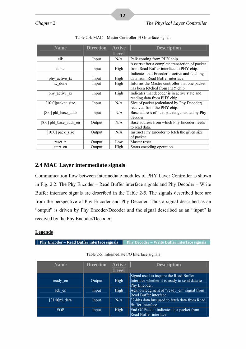
2.4 MAC Layer intermediate signals
Communication flow between intermediate modules of PHY Layer Controller is shown
in Fig. 2.2. The Phy Encoder – Read Buffer interface signals and Phy Decoder – Write
Buffer interface signals are described in the Table 2-5. The signals described here are
from the perspective of Phy Encoder and Phy Decoder. Thus a signal described as an
“output” is driven by Phy Encoder/Decoder and the signal described as an “input” is
received by the Phy Encoder/Decoder. Legends
Phy Encoder – Read Buffer interface signals Phy Decoder – Write Buffer interface signals
Table 2-5: Intermediate I/O Interface signals
Name Direction Active Level
Description
ready_en
Output
High
Signal used to inquire the Read Buffer Interface whether it is ready to send data to Phy Encoder.
ack_en Input High Acknowledgment of “ready_en” signal from Read Buffer interface.
[31:0]rd_data Input N/A 32-bits data bus used to fetch data from Read Buffer Interface.
EOP Input High End Of Packet: indicates last packet from Read Buffer interface.

Chapter 2 The Physical Layer Controller
13
valid Input High Indicates valid data at “rd_data” bus of Read Buffer interface
buf_if_active_en Input High It signifies that Read Buffer is in active state and fetching data from dprf.
phy_rd_valid Output High Indicates valid data, at 32-bits RxData bus, to Write Buffer Interface.
ready_de
Output
High
Signal used to inquire the Write Buffer Interface whether it is ready to receive data from Phy Decoder.
[31:0]phy_wr_data_bus
Output
N/A
32-bits data bus; used to write data into Write Buffer interface.
phy_data_last Output High Indicates last packet from PHY chip buf_if_active_de Input High It signifies that Write Buffer is in active state
and writing data into dprf. ack_de Input High Acknowledgment of “ready_de” signal from
Write Buffer interface.
2.5 Algorithmic States Machine Description of Phy Encoder
ASMD of PHY Encoder is shown in Fig. 2.3. When an encoding process is done by
Link Layer controller, it asserts “ll_enc_done” (mentioned in Chapter 6, The Master
Controller), informing master controller that a valid data has been placed in dprf and
must be fetched by Phy Encoder. Master controller then asserts “start_en” signal to
initialize Phy encoder and waits for being acknowledged from Phy encoder.
LTSSM controls the power state of PHY chip through Phy Encoder. Phy chip remains
idle in P1 and P3 power states. In P2 state, encoder waits for the instruction from
LTSSM either to force Phy Chip to transmit LFPS or to do receiver detection operation
(Fig. 2.3). When a valid data is present in the buffers, LTSSM instructs Phy Encoder to
take Phy chip into P0 state. Encoder starts the process of fetching data, from buffer,
only when a positive edge of “transmit” is seen asserted.
When LTSSM asserts “transmit” signal, encoder requests the data and waits for the
acknowledgment from Read Buffer Interface. When transaction begins, encoder obtains
the data payload size from the packet size (given by master controller, in terms of bytes)
and puts into the register “[10:0] data_pld_size”. The purpose of calculating the data
payload size is to find out how many number of transactions are required to send the
complete packet to Phy chip. Since each transaction can have 4 symbols of transmit data
(32-bit bus), therefore a packet size is divided by 4 to obtain the correct number of
transactions required.

Chapter 2 The Physical Layer Controller
14
As mentioned in section 2.3.1 (Table 2.1), TxDataK bus indicates Control or Data byte
in a current transaction. The RTL of encoder is efficient enough to locate which byte is
a control byte or data byte in a current transaction. Fig 2.4 depicts that there are two
such transactions (1st and 6th) which have complete control symbols (bytes) in it. The
last transaction should have all control bytes, but it depends on the data payload size. If
data payload size is not a multiple of 4, then there must be an ambiguity which symbol
is a control or a data byte, in 2nd last transaction. Two least significant bits of “[10:0]
data_pld_size” indicates the position of data byte in 2nd last transaction (Fig. 2.3).

Chapter 2 The Physical Layer Controller
15
Fig. 2.3: ASMD of Phy Encoder

Chapter 2 The Physical Layer Controller
16
Fig. 2.4: Standard packet with maximum of 1024 data bytes
2.6 Algorithmic States Machine Description of Phy Decoder
ASMD of Phy Decoder is shown in Fig. 2.5. “PowerState” of Phy Decoder is again in a
control of LTSSM. Phy Decoder remains idle in P1 & P2 states. In P3, LTSSM asserts
“receiver_DO” signal when it requires “receiver detection” operation to be performed.
Phy Decoder in-turn asserts “TxDetectRx” signal, requesting PHY chip to begin
“receiver detection” operation. This signal should remain high until “phy_status” signal
from Phy Chip is seen asserted. When the receiver detection operation is completed,
PHY chip asserts “phy_status” signal. Phy decoder then deasserts “TxDetectRx”,
meanwhile informs LTSSM, the status of receiver through “Rx_status_2LTSSM” bus.
As soon as LTSSM instructs Phy decoder to take PHY Chip into the power state P0,
decoder starts looking for “Rx_elec_idle” signal. Phy Decoder informs the LTSSM
about LFPS on the basis of “Rx_elec_idle” signal. It then goes into “idle” state until
valid data is present at “RxData” bus. When the valid data is present, decoder
interrogates the Write Buffer Interface”, whether it is ready to accept the incoming data,
and jumps to the “ackldg” (acknowledge) state. It then waits for the acknowledgment
from “Write Buffer Interface”. As soon as the buffer acknowledges, decoder starts
fetching and sending data from Phy Chip to Write Buffer Interface respectively (see Fig.
2.2).

Chapter 2 The Physical Layer Controller
17
Fig. 2.5: ASMD of Phy Decoder

Chapter 2 The Physical Layer Controller
18
Phy Decoder keeps on transferring packet from Phy Chip to Write Buffer Interface
unless the Link Layer Controller asserts “ignore” signal. When “ignore” is seen
asserted, Phy decoder discards the incoming data from the Phy Chip and starts looking
for LRTY. Decoder also calculates the size of packet while transferring data from Phy chip to write
buffer interface. Fig. 2.4 depicts that a packet can have a maximum size of 1024 bytes
(max data payload) + 28 bytes (standard protocol of each packet). The packet size is
calculated in such a way that a counter is incremented each time a transaction occurs.
Decoder continuously monitors RxDataK lines. Control byte is indicated by RxDataK
bus whenever its value is non-zero. Whenever a non-zero value is present at RxDataK
lines, another counter is incremented to monitor the number of control byte transactions.
Referring to the Fig. 2.4, it can be observed that there could only be 3 or 4 such
transactions which have control bytes in it, i.e. the first transaction, the sixth transaction
and the last transaction. There could be fourth control byte transaction when data
payload size is not a multiple of 4 (i.e. first three of the last four control bytes can be a
part of second last transaction).
Since the first and the sixth transaction is a complete control byte transaction, therefore
one doesn’t need to care about them. The problem arises after data pay load due to
variations in the data payload sizes.
Fig 2.5 reveals that decoder repeatedly checks for “rxdataK_count” to become equal to
2. When “rxdataK_count” become equal to 2, decoder checks the value of RxDataK.
RxDataK = 4’hF point towards that all the four bytes are control bytes and a current
transaction is End of Packet. RxDataK, other than 4’hF, clearly indicates that the data
payload size is not a multiple of 4 and the present transaction contains the data byte(s)
besides the control byte(s) as well. Also we would have fourth control byte transaction.
If RxDataK = 4’h8 (4’b1000), it shows, there are 3 data bytes and 1 control byte. This
one control byte is actually from the four of the last control bytes (shown in Fig. 2.4).
This means that there will be only 3 (remaining) control bytes in the next transaction
and the last byte will remain empty, thus a value of 1’b1 is subtracted from the size of
packet (shown in Fig. 2.5). Similar method is implemented for RxDataK = 4’hC and
4’hE.

Chapter # 3
The Link Layer
Chapter 3 The Link Layer
19
3.1 Link Layer Overview
A SuperSpeed link is a logical and physical connection of two ports. The connected
ports are called link partners. A port has a physical part and a logical part. The link layer
defines the logical portion of a port and the communications between link partners. The
responsibilities of link layer contain successful data transfer with the link partner and
link training control. The robust link flow control is based on packets and link
commands. Link management between partners and the flow control is completely
governed by the link command words.
3.2 Hardware Implementation of Link Layer
Fig. 3.1: Block Diagram of the Link Layer

Chapter 3 The Link Layer
20
3.2.1 Packet Disassembler
This module is associated with the decoding of the packets, which are received from the
link partners, link layer and protocol layer both contains this disassembler but
differentiate in the extraction of information link layer is more interested in the error
free transaction so it checks the CRC 16 and CRC 5 of the header packets to endorse it
and the Header Sequence # to verify the flow of the transaction and asks the Link Layer
controller to acknowledge the particular HP with LGOOD or reject a corrupted HP with
LBAD.
3.2.2 Packet Assembler
Link Layer controller fetches the data from Dual Port memory bank 1 where already
assembled data is placed by the protocol layer and place the link control word in the
header packet. HP are of 20 bytes which are constructed in link layer by the addition of
Link Control Word (2 Bytes) and Header Packet Framing HPSTART ordered set
defined as three consecutive symbols of SHPs (Start Header Packet) followed by a
symbol of EPF (End Packet framing) while CRC 16 and header information collectively
called as Packet header is added in the protocol layer. The assembled packet is then
write in the Dual port memory bank 3.The complete HP structure is shown in figure .1.
Fig. 3.2: Header packet with HPSTART, Packet Header and Link Control Word
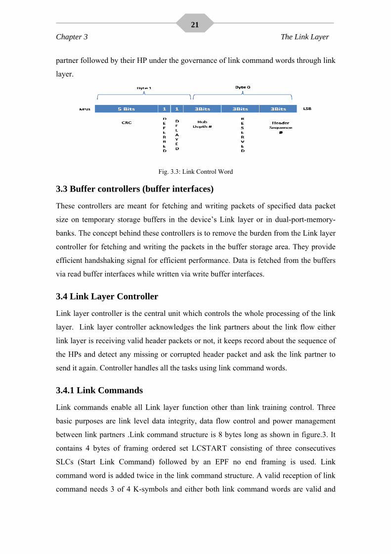
Link control word is also generated in the link layer which is 16 bits long, which
contains 11 bits of information and 5 bits for CRC 5 as shown in figure .2. Header
Sequence # is unique to each link which is used for integrity assurance of the link and
detect the missing HP while CRC-5 protects the integrity of other 11 bits. Delayed,
deferred and Hub Depth bits are utilized for Hub forwarding support. Data packet
payloads are generated and framed in the protocol layer but transferred to the link
Chapter 3 The Link Layer
21
partner followed by their HP under the governance of link command words through link
layer.
Fig. 3.3: Link Control Word
3.3 Buffer controllers (buffer interfaces)
These controllers are meant for fetching and writing packets of specified data packet
size on temporary storage buffers in the device’s Link layer or in dual-port-memory-
banks. The concept behind these controllers is to remove the burden from the Link layer
controller for fetching and writing the packets in the buffer storage area. They provide
efficient handshaking signal for efficient performance. Data is fetched from the buffers
via read buffer interfaces while written via write buffer interfaces.
3.4 Link Layer Controller Link layer controller is the central unit which controls the whole processing of the link
layer. Link layer controller acknowledges the link partners about the link flow either
link layer is receiving valid header packets or not, it keeps record about the sequence of
the HPs and detect any missing or corrupted header packet and ask the link partner to
send it again. Controller handles all the tasks using link command words.
3.4.1 Link Commands
Link commands enable all Link layer function other than link training control. Three
basic purposes are link level data integrity, data flow control and power management
between link partners .Link command structure is 8 bytes long as shown in figure.3. It
contains 4 bytes of framing ordered set LCSTART consisting of three consecutives
SLCs (Start Link Command) followed by an EPF no end framing is used. Link
command word is added twice in the link command structure. A valid reception of link
command needs 3 of 4 K-symbols and either both link command words are valid and

Chapter 3 The Link Layer
22
identical or one Link command word is valid and the other is invalid. In USB3.0 we use
three types of link command words for different usage as shown in table 3-1.
Fig. 3.4: Link Command Structure
Table.3-1: Types of Link Commands
Usage Cases Link Commands
Ensure Successful Transfer Of HP
(Acknowledgement)
LGOOD_n(n=0to7), LBAD, LRTY
Flow Control LCRD_x(x=A,B,C,D)
Power Management LGO_Ux(x=1,2,3), LAU, LXU,
LPMA
Special (For presence in U0) LUP
LGOOD:
This is an acknowledgement from a link partner that a header packet with the Header
Sequence Number of “n” is received properly. LGOOD_n uses an explicit numerical
index called Header Sequence Number to represent the sequencing of a header packet.
The Header Sequence Number starts from 0 and is incremented by one based on
modulo-8 addition with each header packet. The index corresponds to the received
Header Sequence Number and is used for flow control and detection of lost or corrupted
header packets.
LBAD:
LBAD commands are used for Bad header packet. LBAD is sent by a port receiving the
header packet in response to an invalid header packet. Packet that was received has
corrupted CRC-5 and/or CRC-16.

Chapter 3 The Link Layer
23
Receipt of LBAD will cause a port to resend all header packets after the last header
packet that has been acknowledged with LGOOD_n.
LRTY:
Sent by a port before resending the first header packet in response to receipt of LBAD.
LCRD:
Sent by a port after receiving a header packet that meets the following criteria:
• LGOOD_n is sent.
• The header packet has been processed, and an Rx Header Buffer Credit is available.
LCRD_x is sent in the alphabetical order of A, B, C, D, and back to A without skipping.
Missing LCRD_x
will cause the link to transition to Recovery.
LGO_Ux:
LGO_U1 Sent by a port requesting entry to U1.
LGO_U2 Sent by a port requesting entry to U2.
LGO_U3 Sent by a downstream port (Host) requesting entry to U3. An upstream
port (Device) shall accept the request.
LAU:
Sent by a port accepting the request to enter U1, U2, or U3.
LXU:
Sent by a port rejecting the request to enter U1 or U2.
LPMA:
Sent by a port upon receiving LAU. Used in conjunction with LGO_Ux and LAU
handshakes to guarantee both ports are in the same state.
LUP:
It is a special link command use to signify that device is present in U0. Sent by an
upstream port every 10 μs when there are no packets or other link commands to be
transmitted.
3.4.2 Header Packet Exchange Control
Both link partners contains 4 buffers in each transmitter and receiver, these buffers have
the capacity to hold four HPs at a time. In order to explain HP exchange procedures

Chapter 3 The Link Layer
24
among two link partners some terminologies and link commands should be explained
first.
RX Header Sequence Number: The sequence number of the expected HP from TX.
TX Header Sequence Number: The sequence number assigned to new HP.
ACK_TX Header Sequence Number: Oldest unacknowledged HP in TX buffer.
Local RX Header Buffer Credit: Space available in RX HP buffer.
Remote RX Header Buffer Credit: Credit to transmit HPs.
RX LCRD Index: Assigned to next LCRD_x.
Remote RX LCRD index: Expected index of next LCRD_x from RX.
Link Partner: Device at one end of the link.
Link Partner TX: HP sender.
Link Partner RX: HP receiver.
3.4.2.1 IDLE STATE
TX HP BUF F E REmpty
Empty
Empty
Empty
TX HP BUF F E REmpty
Empty
Empty
Empty
R X HP BUF F E REmpty
Empty
Empty
Empty
R X HP BUF F E REmpty
Empty
Empty
Empty
R X Header S equence # : 0
L C RD Index: A
L ocal RX Header Buffer c redit: 4
R X Header S equence # : 0
L C RD Index: A
L ocal RX Header Buffer c redit: 4
TX Header S equence #: 0
AC K Header S equence#: 0
R emote RX Header Buffer C redit: 4
R emote RX L C RD Index: A
TX Header S equence #: 0
AC K Header S equence#: 0
R emote RX Header Buffer C redit: 4
R emote RX L C RD Index: A
L ink Partner TX L ink Partner RX
LUP
L UP
L UP
Fig. 3.5: Initial Condition and Idle State
The link has just entered the U0 state from reset hence initial values of above described
parameters are set as shown in the figure3.5. It is clear that so far no HP is transmitted

Chapter 3 The Link Layer
25
or received between link partners. Hence there is no exchange of packets or link
command words but working in U0 this is an IDLE state so LUP command word is
transmitted by upstream port after every 10us to aid the disconnect detection . When a
header packet will be transmitted by the TX link partner LUP transmission will be
automatically ended.
3.4.2.2 Initialization for HP integrity and flow control
Whenever the link state transition back to U0 initialization using advertisement is done
to announce the link partner about parameters, header sequence number and header
buffer credit is advertised.
• Advertise expected RX Header Sequence Number, send LGOOD_n,where
n=HSEQ# of last good received HP other wise.
• Advertise Local RX Header Buffer Credit,send credit for all available buffers
using LCRD_x.
3.4.2.3 Valid Header Packets Exchange
TX HP BUFF E REmpty
HS E Q#=1,Acknowledged
HS E Q#=2,UnAcknowledged
Empty
TX HP BUFF E REmpty
HS E Q#=1,Acknowledged
HS E Q#=2,UnAcknowledged
Empty
R X HP BUFF E REmpty
HS E Q#=1,P roces s ing Done
HS E Q#=2,C hecking OK
Empty
R X HP BUFF E REmpty
HS E Q#=1,P roces s ing Done
HS E Q#=2,C hecking OK
Empty
R X Header S equence # : 3
L C RD Index: B
L ocal RX Header B uffer c redit: 2
RX Header S equence # : 3
L C RD Index: B
L ocal RX Header B uffer c redit: 2
TX Header S equence #: 3
AC K Header S equence#: 2
R emote RX Header B uffer C redit: 2
R emote RX L C RD Index: B
TX Header S equence #: 3
AC K Header S equence#: 2
R emote RX Header B uffer C redit: 2
R emote RX L C RD Index: B
L ink Partner TX L ink Partner RXHP,HS E Q#0
L GOOD_
0
HP ,HS E Q#1
L GOOD
_1
L C RD_A
HP ,HS E Q#2
Fig. 3.6: Successful Transmission & Reception of HP
Fig. 3.6 shows the successful transmission and rececption of HP.All the parameter
values are updated accordingly.Three HPs are sent by the Link PartnerTX HP#0,HP#1
and HP#2. LGOOD of HP#0 and HP#1 has been received so these packets are
acknowldeged, HP#0 is removed from the buffer because LCRD was received for that

Chapter 3 The Link Layer
26
HP#0, but HP#2 is still unacknowledged because it is being checked for errors,as
checking of HP#2 is also done valid, LGOOD for HP#2 is also about to send.
3.4.2.4 Header Packet Retry Process
TX HP BUF F E RHS E Q#=0,Acknowledged
HS E Q#=1,Unacknowledge
HS E Q#=2,Unacknowledged
Empty
TX HP BUF F E RHS E Q#=0,Acknowledged
HS E Q#=1,Unacknowledge
HS E Q#=2,Unacknowledged
Empty
R X HP BUF F E RHS E Q#=0, Proces s ing Done
HS E Q#=1, C RC 5 E rror
HS E Q#=2, C hecking OK
Empty
R X HP BUF F E RHS E Q#=0, Proces s ing Done
HS E Q#=1, C RC 5 E rror
HS E Q#=2, C hecking OK
Empty
R X Header S equence # : 1
L C RD Index: B
L ocal RX Header Buffer c redit: 3
RX Header S equence # : 1
L C RD Index: B
L ocal RX Header Buffer c redit: 3
TX Header S equence #: 1
AC K Header S equence#: 1
R emote R X Header Buffer C redit: 3
R emote R X L C RD Index: B
TX Header S equence #: 1
AC K Header S equence#: 1
R emote R X Header Buffer C redit: 3
R emote R X L C RD Index: B
L ink Partner TX L ink Partner RXHP ,HS E Q#0
HP ,HS E Q#1
L BAD
HP ,HS E Q#2
L GOOD_
0
L R TY
Fig. 3.7: Transmission of a corrupted HP
Figure 3.7 explains how a link layer controller will detect a corrupted header packet and
ask the link partner to resend packets again .Link partner has transmitted 3 header
packets HP#0 has been acknowledged but still waiting for LCRD to be removed from
the buffer .HP#1 and HP#2 are still unacknowledged and waiting for their LGOOD but
HP#1 is a corrupted header packet because it generated CRC5 error so LBAD is send
from Link Partner RX to Link Partner TX, after reception of LBAD TX will generate
LRTY for RX which means it is trying to resend the corrupted header packet but not
only corrupted HP but all unacknowledged HPs will be resend again to the RX ,HP#2
was a valid HP as it encounter no error in error checking but because of HP#1 it has to
be resend again. Until the reception of LRTY link partner RX will ignore all received
Chapter 3 The Link Layer
27
HP. Several types of header packet errors are detected and they are resolved using
different methods else they made the link to transition to recovery. They are:
1. Missing of a header packet
2. Invalid header packet due to CRC errors
3. Mismatch of a Rx Header Sequence Number
4. Mismatch of ACK Header Sequence Number.
5. Missing of frames.
3.4.3 Link Power Management
Requests to transition to low power link states are done at the link level during U0. Link
commands LGO_U1, LGO_U2, and LGO_U3 are sent by a port as a request to enter a
low power link state. LAU or LXU is sent by the other port as the response. LPMA is
sent by a port in response only to LAU.
3.4.3.1 Rules for a port to request or accept a low power link state
It has transmitted LGOOD_n, LCRD_x for all packets received.
• It has received and LGOOD_n, LCRD_x sequence for all packets transmitted.
• It has no pending packets for transmission.
• It is permitted to request or accept by the highest layer
• U3 is initiated only by software request to a downstream port, it must be
accepted.
3.5 Error Detection Algorithm (CRC)
Every modern communication protocol uses one or more error detection algorithms.
Cyclic Redundancy Check, or CRC, is by far the most popular one. CRC properties are
defined by the generator polynomial length and coefficients. The protocol specification
usually defines CRC in hex or polynomial notation. For example, CRC5 used in USB
3.0 protocol is represented as 0×5 in hex notation or as G(x)=x5+x2+1 in the
polynomial notation. Other CRC used in USB3.0 are CRC16 and CRC32 .CRC is
typically implemented in hardware as a linear feedback shift register (LFSR) with a
serial data input as shown in the Fig. 3.8.

Chapter 3 The Link Layer
28
Fig. 3.8: CRC5 Serial Remainder Generation Serial LFSR implementation of the CRC is suboptimal because of the serial data input it
only allows the CRC calculation of one data bit every clock. If a design has 32-bit wide
data path, meaning that every clock CRC module has to calculate CRC on 32-bit of
data, this approach will not work. To achieve higher throughput, serial LFSR
implementation of the CRC has to be converted into a parallel N-bit wide circuit, where
N is the design data path width, so that every clock N bits are processed. This is called
as parallel CRC implementation.
3.5.1 Method of Parallel CRC Computation
The method description is step-by-step and is accompanied by an example of parallel
CRC generation for the USB CRC5 polynomial G(x)=x5+x2+1 with 11-bit data width.
1. Let’s denote N=data width, M=CRC polynomial width. For example, if we want to
generate a parallel USB CRC5 for 11-bit data path, N=11, M=5.
2. Implement serial CRC generator of polynomial (00101b) in any language or
multisim.
3. Parallel CRC implementation is a function of N-bit data input as well as M-bit
current CRC state. In the following steps we’re going to build two matrices:
a) Mout (next CRC state) as a function of Min (current CRC state) when Nin=0.
This matrix is of size [MxM].
b) Mout as a function of Nin when Min=0. This matrix is of size [NxM]
4. Using the routine from step (2) calculate the CRC for the N values of Nin when
Min=0. Each of the Nin values is one-hot encoded, that is there is only one bit set.
Mout = CRC (Nin, Min=0).
Chapter 3 The Link Layer
29
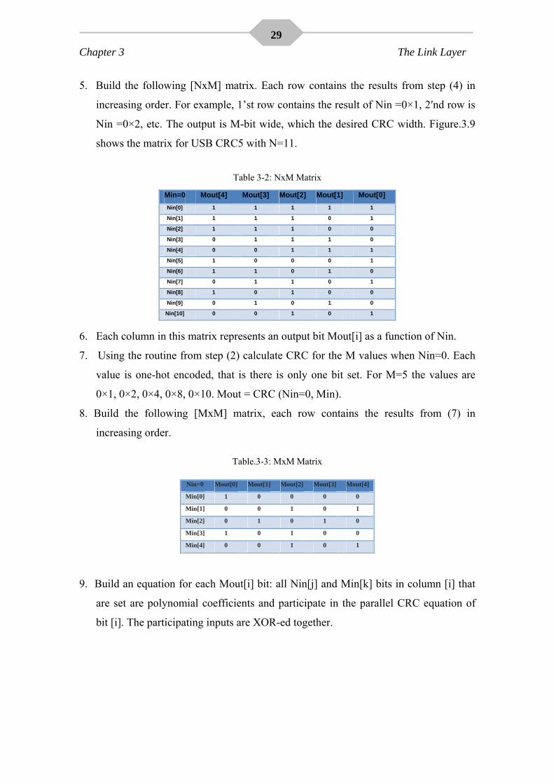
5. Build the following [NxM] matrix. Each row contains the results from step (4) in
increasing order. For example, 1’st row contains the result of Nin =0×1, 2′nd row is
Nin =0×2, etc. The output is M-bit wide, which the desired CRC width. Figure.3.9
shows the matrix for USB CRC5 with N=11.
Table 3-2: NxM Matrix
Min=0 Mout[4] Mout[3] Mout[2] Mout[1] Mout[0] Nin[0] 1 1 1 1 1
Nin[1] 1 1 1 0 1
Nin[2] 1 1 1 0 0
Nin[3] 0 1 1 1 0
Nin[4] 0 0 1 1 1
Nin[5] 1 0 0 0 1
Nin[6] 1 1 0 1 0
Nin[7] 0 1 1 0 1
Nin[8] 1 0 1 0 0
Nin[9] 0 1 0 1 0
Nin[10] 0 0 1 0 1
6. Each column in this matrix represents an output bit Mout[i] as a function of Nin.
7. Using the routine from step (2) calculate CRC for the M values when Nin=0. Each
value is one-hot encoded, that is there is only one bit set. For M=5 the values are
0×1, 0×2, 0×4, 0×8, 0×10. Mout = CRC (Nin=0, Min).
8. Build the following [MxM] matrix, each row contains the results from (7) in
increasing order.
Table.3-3: MxM Matrix
Nin=0 Mout[0] Mout[1] Mout[2] Mout[3] Mout[4]
Min[0] 1 0 0 0 0
Min[1] 0 0 1 0 1
Min[2] 0 1 0 1 0
Min[3] 1 0 1 0 0
Min[4] 0 0 1 0 1
9. Build an equation for each Mout[i] bit: all Nin[j] and Min[k] bits in column [i] that
are set are polynomial coefficients and participate in the parallel CRC equation of
bit [i]. The participating inputs are XOR-ed together.
Chapter # 4
The Link Training and Status State Machine
(The LTSSM)

Chapter 4 The LTSSM
31
4.1 Introduction
The USB 3.0 architecture utilizes very efficient and productive algorithms for
maintaining reliable link, highly optimized power consumption and extremely fast and
flawless data transfer rate. The Link Training Status State Machine has been employed
as the foremost workhorse in these regards. Its functions and provisions contribute
matchlessly towards the “super speed” high class performance, delivered by USB 3.0.
The LTSSM tunes and trains the USB link for reliable data transfer. It also implements
various algorithms for link’s reliability maintenance and is also responsible to recover
the link from any errors as may arise. It also plays key role in power management by
greatly reducing link’s power consumption and nullifying any conditions that waste
power. The LTSSM allows or disallows data transaction over the USB 3.0 link based
upon the device state and the adopted power saving scheme. It blocks data path when
the device undergoes a serious error and then performs the error recovery itself. Then
when the link is ready to send or transmit data, it is the LTSSM that allows the data to
be communicated over the link. The LTSSM also performs operations for making the
link ready for data transaction in the very beginning when the device is plugged in.
Hence LTSSM is the “DATA FLOW GATEWAY CONTROL” for the device.
The core responsibilities of the LTSSM include:
• Link Training & Initialization
• Power Management
• Error Recovery
For the sake of performing these duties, it communicates and co-ordinates with almost
all the layers of the device namely the PHY, the MAC, the link layer and also the master
controller. Thus it behaves as the central traffic controller for the device. A brief
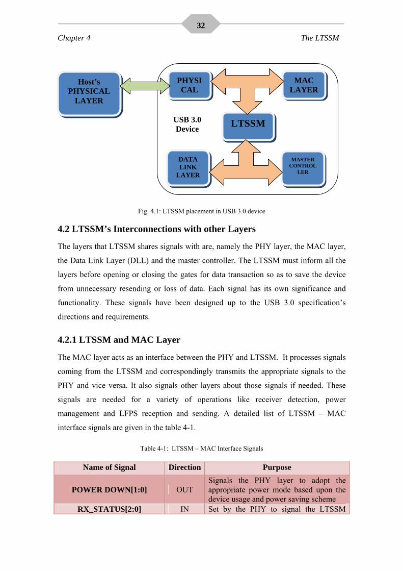
overview of the placement and interconnection of LTSSM with other layers is shown in
the Fig. 4.1.
Chapter 4 The LTSSM
32
USB 3.0 DEVIC
E
Host’s PHYSICAL
LAYER
DATA LINK
LAYER
MAC LAYER
PHYSICAL
MASTER CONTROL
LER
LTSSM
Fig. 4.1: LTSSM placement in USB 3.0 device
4.2 LTSSM’s Interconnections with other Layers
The layers that LTSSM shares signals with are, namely the PHY layer, the MAC layer,
the Data Link Layer (DLL) and the master controller. The LTSSM must inform all the
layers before opening or closing the gates for data transaction so as to save the device
from unnecessary resending or loss of data. Each signal has its own significance and
functionality. These signals have been designed up to the USB 3.0 specification’s
directions and requirements.
4.2.1 LTSSM and MAC Layer
The MAC layer acts as an interface between the PHY and LTSSM. It processes signals
coming from the LTSSM and correspondingly transmits the appropriate signals to the
PHY and vice versa. It also signals other layers about those signals if needed. These
signals are needed for a variety of operations like receiver detection, power
management and LFPS reception and sending. A detailed list of LTSSM – MAC
interface signals are given in the table 4-1.
Table 4-1: LTSSM – MAC Interface Signals
Name of Signal Direction Purpose
POWER DOWN[1:0] OUT Signals the PHY layer to adopt the appropriate power mode based upon the device usage and power saving scheme
RX_STATUS[2:0] IN Set by the PHY to signal the LTSSM
USB 3.0 Device
Chapter 4 The LTSSM
33
about presence or absence of a far end receiver
PHY_STATUS IN Set by the PHY to signal completion of receiver detection
LFPS_RECEIVED IN Set by the MAC to signal the LTSSM about the reception of LFPS signals.
TRANSMIT_LFPS OUT Set by the LTSSM when it desires to send the LFPS(Low Frequency Periodic Signal)
RX_TERMINATION OUT Set by the LTSSM to enable or disable the PHY’s termination resistors.
TRANSMIT OUT Set by the LTSSM when it is ready to allow MAC to carry out packet transactions.
VBUS IN Set by MAC to signal the LTSSM about presence or absence of power signal (vbus).
RECEIVER _DO OUT Set by the LTSSM to signal the PHY to initiate receiver detection
SEND_IDLE IN Set by the MAC to signal the sending of IDLEs
4.2.2 LTSSM and PHY Chip
The LTSSM also shares some direct signals with the PHY chip where MAC’s
interception is not necessary ant might overload MAC with extra tasks. These signals
enable the LTSSM to control the PHY directly when MAC or other layers are inactive
for the purpose of its own transactions, thereby reducing device’s power consumption
and increasing the efficiency. Such needs arise during link training and error recovery.
Table 4.-2: LTSSM – PHY Interface Signals
Name of Signal Direction Purpose TX [31:0] OUT Used to send 32-bit data to the host when needed
TX_K [3:0] OUT Used to send 4-bit data K word to the host in accordance with the “Tx” signal.
RX [31:0] IN Used to receive 32-bit data to the host when needed
RX_K [3:0] IN Used to receive 4-bit data K word to the host in accordance with the “Rx” signal.
RX_VALID IN Set by host to signal valid data reception
RX_EQ_TRAIN OUT Used to direct the PHY to bypass normal operations and perform receiver equalization
RESET_B IN Used to reset the device registers and buffers

Chapter 4 The LTSSM
34
CLK IN Provided by PHY as the operational clock frequency
TX_ELEC_IDLE OUT Set by LTSSM to start or stop data transaction
4.2.3 LTSSM and Data Link Layer
The Data Link layer frequently needs to communicate with the LTSSM during various
operations. It signals the LTSSM about the emergence of any link error that must drive
the LTSSM into error recovery procedures. The link layer also needs to tell the LTSSM
about any link power management commands from the host that might need LTSSM’s
intervention since almost all the power optimization is catered by the LTSSM. The
detailed list of LTSSM – DLL interface signals is given in the table 4-3.
Table 4-3: LTSSM – DLL Interface Signals
Name of Signal Direction Purpose
LGO_U1 IN Used to send the LTSSM to U1 from U0 LGO_U2 IN Used to send the LTSSM to U2 from U0 LGO_U3 IN Used to send the LTSSM to U3 from U0
LL_ADV_DONE IN Used to tell the LTSSM that U0 advertisement has been done
COMM_SENT IN To tell the LTSSM that command or data packets are being sent
SEND_LUP_EN OUT Used to instruct the DLL to send LUP link command word
ERROR_LL IN Used to tell the LTSSM to proceed to error recovery mode
U0 OUT Used to tell the device that device is in U0 RECOVERY_U0 OUT Used to tell DLL that U0 has been entered via
recovery
4.3 An Overview Of The LTSSM State Machine
The state machine of LTSSM is specified with 12 main states that carry out these
responsibilities. Four of these states are solely for power management. These four states
include U0, U1, U2, and U3. These four states provide different levels of energy saving
schemes U0 being the active most state having all the modules in the device active,
while U3 being the most dormant state with maximum power saving facilities, though at
a higher latency rate. The U1, and U2 are intermediate power states that provide certain
Chapter 4 The LTSSM
35
selective levels of power saving. Compared with U1, U2 allows for further power
saving opportunities with a penalty of increased exit latency. U3 is a link suspended
state where aggressive power saving opportunities is possible. The USB 3.0 has been
designed for maximum power saving, rendering the device completely inactive or
“sleeping” when not in use. This enhances up time for portable devices e.g. laptops etc.
The link training and initialization states are 2 in number namely RX DETECT and
POLLING. The RX DETECT state is designated for the link’s far end receiver detection
where as POLLING is mainly reserved for link training and receiver aligning.
RX.DETECT represents the initial power-on link state where a port is attempting to
determine if its SuperSpeed link partner is present. POLLING is a link state that is
defined for the two link partners to have their SuperSpeed transmitters and receivers
trained, synchronized, and ready for packet transfer.
The error recovery states are RECOVERY and COMPLIANCE. These states are
entered in case of any sort of miss matching of synchronization or malfunctioning.
Another state is LOOPBACK which is used as a ping to check the reliability and
operation of the receiver and transmitter. Next come two states that result in case of
recovery failure or when the device is disconnected. These states are SS.DISABLED
which is entered when device is completely rendered inactive or is disconnected, and
the SS.INACTIVE state which is entered when the device cannot operate in “super
speed” mode. In the last comes the HOT RESET mode which is entered when the host
desires to reset the device. The state machine of LTSSM can also be well described by a
state diagram in Fig. 4.2.
4.4 Detailed Description of LTSSM States
4.4.1 SS. DISABLED
It is a state where a port’s SuperSpeed connectivity is disabled with its receiver
termination removed. SS.Disabled is also a logical power-off state for a self-powered
USB device. The port does not receive or transmit any USB signals in this mode. Only
VBUS is detectable in this state.

Chapter 4 The LTSSM
36
4.4.2 SS. INACTIVE
This mode is entered as a result of far end receiver removal or other non recoverable
errors. During SS.Inactive, a port periodically performs a far-end link partner detection.
If a link partner is not detected, the device will return to RX.DETECT. Otherwise, the
link will stay in SS.Inactive until software intervention is made by issuing a warm reset.
The SS.INACTIVE contains sub states which are mentioned in the SS.INACTIVE state
machine (Fig. 4.3).
Fig. 4.2: LTSSM State Machine Diagram.

Chapter 4 The LTSSM
37
Fig. 4.3: SS.INACTIVE Sub state Machine
4.4.3 RX.DETECT
Rx.Detect is the power on state of the LTSSM for a USB device that is entered after
PowerOn Reset and Warm Reset, used to detect the impedance of far-end receiver. A
port will perform the far-end receiver termination detection periodically during
Rx.Detect. If the link partner is detected the LTSSM transitions to the link training state
called POLLING. Otherwise it stays in RX.DETECT. The RX.DETECT substate
machine is shown in the Fig. 4.4.
Fig. 4.4: RX.DETECT Substate Machine
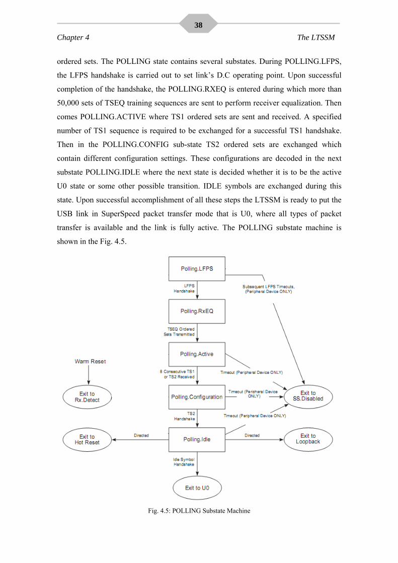
4.4.4 POLLING
Polling is a state for link training. During Polling, a Polling.LFPS handshake shall take
place between the two ports before the SuperSpeed training is started. Bit lock, symbol
lock, and Rx equalization trainings are achieved using TSEQ, TS1, and TS2 training
Chapter 4 The LTSSM
38
ordered sets. The POLLING state contains several substates. During POLLING.LFPS,
the LFPS handshake is carried out to set link’s D.C operating point. Upon successful
completion of the handshake, the POLLING.RXEQ is entered during which more than
50,000 sets of TSEQ training sequences are sent to perform receiver equalization. Then
comes POLLING.ACTIVE where TS1 ordered sets are sent and received. A specified
number of TS1 sequence is required to be exchanged for a successful TS1 handshake.
Then in the POLLING.CONFIG sub-state TS2 ordered sets are exchanged which
contain different configuration settings. These configurations are decoded in the next
substate POLLING.IDLE where the next state is decided whether it is to be the active
U0 state or some other possible transition. IDLE symbols are exchanged during this
state. Upon successful accomplishment of all these steps the LTSSM is ready to put the
USB link in SuperSpeed packet transfer mode that is U0, where all types of packet
transfer is available and the link is fully active. The POLLING substate machine is
shown in the Fig. 4.5.
Fig. 4.5: POLLING Substate Machine

Chapter 4 The LTSSM
39
4.4.5 U0 – LINK ACTIVE
U0 is the normal operational state where packets can be transmitted and received. All
layers are active and working in this state. This state consumes maximum power so this
mode is sustained only as long as Super Speed packet transfer continues or is scheduled
to be made in very near feature. This state moves to lower power states as soon as high
speed packet transfer is not made or needed for a specified time.
4.4.6 U1 – LINK IDLE WITH FAST EXIT
U1 is a low power state where no packets are to be transmitted. This mode is “light
sleep” so it provides fastest transition back to other states. There are two possibilities of
exiting this state. If any packet transfers are needed again within a specified time out
period (U2 inactivity timeout), then it moves back to active state in the response of U1
EXIT LFPS signal, or, if that time out occurs and no activity is needed, it moves to an
even lower power mode U2.
Fig. 4.6: U1 Exit Conditions State Diagram
4.4.7 U2 – LINK IDLE WITH SLOW EXIT
U2 is an even lower power mode that provides even deeper power saving capability but
with an increased wake up time. The device goes into “moderate sleep” so it takes bit
longer than U1 to wake up. U2 can only result to U0 by either link partner when a
packet needs to be transmitted.

Chapter 4 The LTSSM
40
Fig. 4.7: U2 EXIT Conditions State Diagram
4.4.8 U3 – LINK SUSPENDED
It is the deepest low power link state where aggressive power saving is provided but its
exit latency is much higher then other two modes. The device goes into “deep sleep” so
it takes the longest to awake the device. It is entered by host through U0 and can also
exit to U0 only.
Fig. 4.8: U3 EXIT Conditions State Diagram
4.4.9 RECOVERY
The Recovery link state is entered to retrain the link after undergoing a serious error, or
to perform Hot Reset. The process of retraining is almost the same as initial training in
POLLING. However, in this case only TS1 and TS2 ordered sets are transmitted and
not TSEQ. The substate machine for RECOVERY is defined in Fig. 4.9.

Chapter 4 The LTSSM
41
Fig. 4.9: Recovery Substate Machine
4.4.10 LOOPBACK
Loopback is intended for testing the accuracy and compatibility of SuperSpeed receiver
and transmitter and also for fault isolation. Loopback includes a bit error rate test
(BERT) state machine. Loopback master is the port that starts loopback and slave is the
port that replies back.
4.4.11 COMPLIANCE
Compliance Mode is used to test the transmitter for compliance to voltage and timing
specifications. Several different test patterns are transmitted during compliance mode
that is designed for tuning different physical parameters of the physical layer. The
LTSSM transitions to RX.DETECT from this state upon the issuance of Warm Reset.
4.4.12 HOT RESET
The hot reset mode is used by either the device or the host to reset its and the partners
registers and timers, as required during the active data transmission. When the host
initiates reset, it shall transmit TS2 ordered sets with the Reset bit asserted, which is
then followed by the device. Once both ports receive the TS2 ordered sets with the

Chapter 4 The LTSSM
42
Reset bit de-asserted, they shall exit from Hot Reset.Active and return to U0 after
exchanging IDLE symbols.
Fig. 4.10: Hot Reset Substate Machine
4.5 Brief Description Of LTSSM’s Functionalities
4.5.1 Link Training & Initialization
One of the core tasks of the LTSSM is to train and make the USB 3.0 link ready for data
transaction. This process starts with the detection of a link partner at the far end of the
link in the RX.DETCT state. The detection starts as soon as the partner is plugged in to
the bus. Once the far end receiver detection is complete, the LTSSM then starts training
the link for synchronizing with the clock frequency and bit locking, in the POLLING
state, with the transmission and exchanging of TSEQ, TS1 and TS2. These training
sequences contain data bits that are designed to train and align the receivers of two link
partners. First of all TSEQ is sent for a specified number of times, then TS1 sequences
are sent and received as well since the far end partner is also designed to detect and send
back these sequences. Upon a successful handshake of all these link training stages
between the link partners, the link is then brought to the active power state, the U0 state,
where it is ready to carry out all super speed data transmissions and receptions.

Chapter 4 The LTSSM
43
Fig. 4.11: Link Initialization & Training Flow Chart
4.5.2 Power Management
The USB 3.0 architecture manages power consumption in a very peculiar and efficient
manner, which minimize power drainage from the host as long as possible. U0 is the
state where data packets are exchanged at super speed and all other communications are
openly made. As soon as this data transfer operation is completed, and there is no more
data transfer expected or scheduled, the system immediately puts device into lower
power mode, U1. If the link is still idle for a specified time in this period it sweeps to
U2 which provides even more power saving. Upon further idle behavior the device is
brought into deep sleep or “U3” mode which provides maximum power saving features
by turning off even the internal clocks for most modules. The device then stays in this
mode until re-triggered by the host.
4.5.3 Error Recovery
The RECOVERY state defined in LTSSM is entered whenever the link fails the
operation, or faces some errors or miss-matches. This state performs the retraining of
the link and the resets the device for the retrieval of the data transfer mode that it was
formerly in. The COMPLIANCE mode is chiefly meant to check if the receiver and
transmitter are in proper alignment.
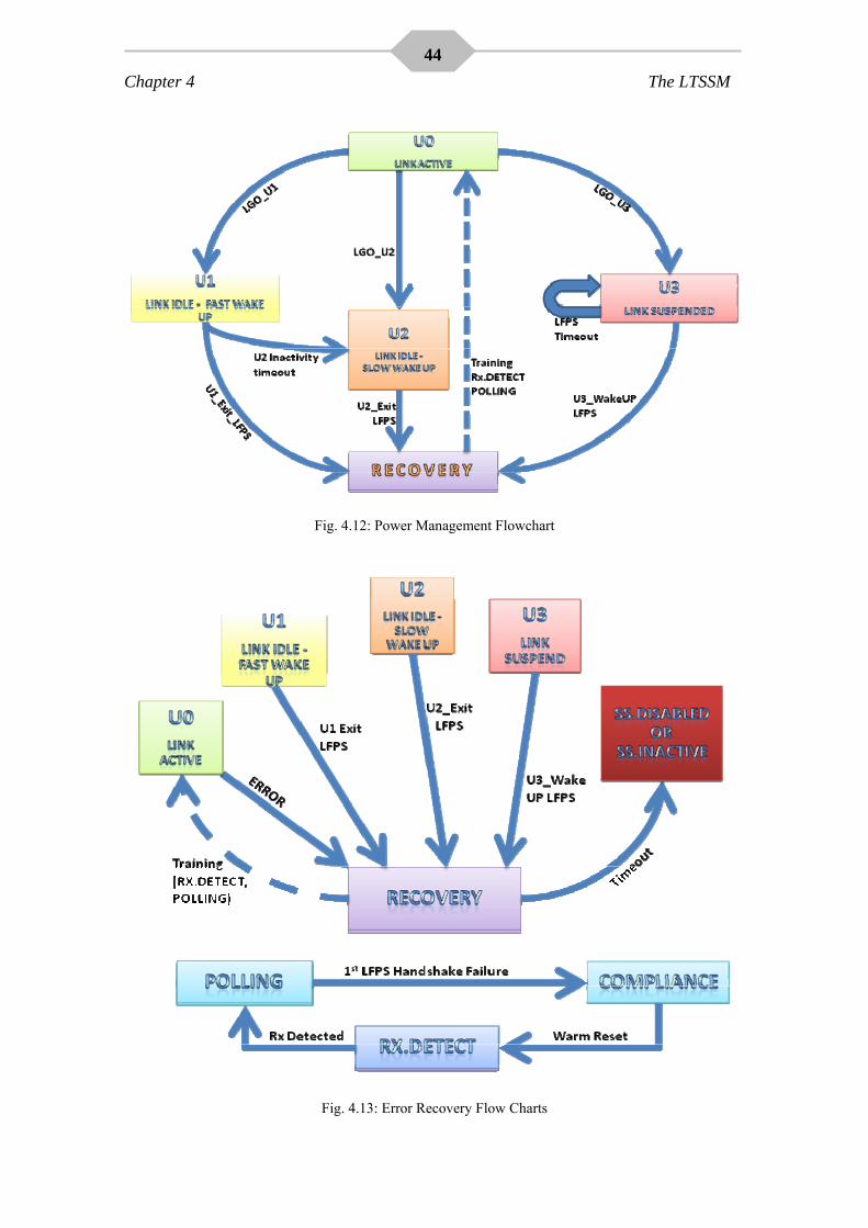
Chapter 4 The LTSSM
44
Fig. 4.12: Power Management Flowchart
Fig. 4.13: Error Recovery Flow Charts

Chapter 4 The LTSSM
45
There are also various timers, counters and sequence senders associated with the
LTSSM that are constantly utilized for LTSSM’s operations. All these timers work
under the reluctances allowed in the specifications. All timeout values must be set to the
specified values after PowerOn Reset or Inband Reset.
The LTSSM is also associated with the very useful provision of USB 3.0, which are the
low frequency periodic signals (LFPS). These signals are of very low power and
perform very important tasks like hand shakes, reset generation and device active
pinging which enable power saving and even higher speeds. These LFPS signals are
characterized on the basis of their timings and repetitions as:
• Polling.LFPS – Sent during POLLING.LFPS as keep alive signal.
• Ping.LFPS – Sent during U1, U2 and COMPLIANCE as keep alive signal.
• U1/U2_EXIT_LFPS – Sent during U1/U2 to transit to recovery and then to U0.
• U3_WAKEUP – Sent during U3 to transit to recovery and then to U0.
• Warm Reset – Used to reset device registers and counters.

Chapter # 5
The Protocol Layer
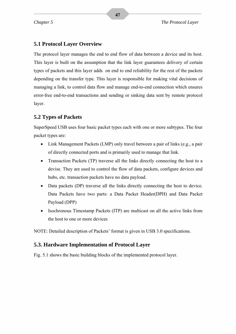
Chapter 5 The Protocol Layer
47
5.1 Protocol Layer Overview
The protocol layer manages the end to end flow of data between a device and its host.
This layer is built on the assumption that the link layer guarantees delivery of certain
types of packets and this layer adds on end to end reliability for the rest of the packets
depending on the transfer type. This layer is responsible for making vital decisions of
managing a link, to control data flow and manage end-to-end connection which ensures
error-free end-to-end transactions and sending or sinking data sent by remote protocol
layer.
5.2 Types of Packets
SuperSpeed USB uses four basic packet types each with one or more subtypes. The four
packet types are:
• Link Management Packets (LMP) only travel between a pair of links (e.g., a pair
of directly connected ports and is primarily used to manage that link.
• Transaction Packets (TP) traverse all the links directly connecting the host to a
devise. They are used to control the flow of data packets, configure devices and
hubs, etc. transaction packets have no data payload.
• Data packets (DP) traverse all the links directly connecting the host to device.
Data Packets have two parts: a Data Packet Header(DPH) and Data Packet
Payload (DPP)
• Isochronous Timestamp Packets (ITP) are multicast on all the active links from
the host to one or more devices
NOTE: Detailed description of Packets’ format is given in USB 3.0 specifications.
5.3. Hardware Implementation of Protocol Layer Fig. 5.1 shows the basic building blocks of the implemented protocol layer.

Chapter 5 The Protocol Layer
48
Fig. 5.1: Block Diagram of the Protocol Layer
5.3.1 Registers bank for Descriptors and Device Configuration
A device needs to be configured before its functionality could be used. The host can
read the device configuration to determine its capabilities and may set alternate settings
for configurations. A device descriptor describes general information about a device. It
includes information that applies globally to the device and all of the device’s
configurations. These register banks are accessed by the host through control transfers
using setup packets. Setup Packets are decoded by the packet disassembler while
protocol layer controller is responsible for fetching or setting these register bank.
5.3.2 Packet assembler
This module is associated with the assembling of packets. It involves the encoding of
header packets- proper placement of header fields’ contents as directed by the protocol
layer controller, crc16 generation and its appending, one word (16-bits) allocation for
link control word, proper placement of the desired data and its crc32 following the Data
Packet Payload (DPP) for DP. The DPP is fetched by the assembler from the SRAM
using read buffer interface and the assembled packets are placed into the dual-port-memory-bank-1 using write buffer interface.

Chapter 5 The Protocol Layer
49
Packet assembler is capable of assembling following packets:
1. Link Management Packets
Following subtypes are supported in the packet assembler
Set link function
U2 inactivity timeout
Port capability
Port configuration response.
2. Transaction Packets
Following subtypes are supported in the packet assembler
ACK
NRDY
ERDY
STALL
DEV_NOTIFICATION
PING_RESPONSE
3. Data Packets
Data packets are responsible for end-to-end data transfer. They don’t have subtypes.
Packet assembler is capable of latching the field required for assembling the packets
each time it is request by controller to assemble the packet so the controller doesn’t
need to drive valid configuration until the packet assembler is done. It provides
necessary hand-shaking signals to protocol layer controller for efficient performance.
NOTE: The assembled packets meet the entire requirements as per specifications.
5.3.3 Packet-disassembler
This module is associated with the disassembling or decoding of packets received from
the remote protocol layer. It involves the extraction of packet’s description i.e. packet
header type, subtype, sequence number etc., detection of crc32 error, DPP aborted, DPP

Chapter 5 The Protocol Layer
50
missing or Data length errors. Packet’s header information, extracted each time when a
valid packet is received, is provided to the protocol layer controller to initiate or resume
appropriate transactions while at the reception of valid data packet, packet-disassembler
either fills the data-buffers with data in DPP or return an appropriate response to the
host(as specified in the USB 3.0 specification). It communicates to the dual-port-
memory-bank-2 through read buffer interface to fetch the packets there while places
DPP, extracted from valid DP, into the SRAM. It provides valid descriptions extracted
from the previous valid disassembled packet until it is instructed to decode another
packet. It is capable of decoding the following packets:
1. Link Management Packets:
Following subtypes are supported in the packet assembler
Set link function
U2 inactivity timeout
Port capability
Port configuration.
2. Transaction Packets
Following subtypes are supported in the packet assembler
ACK
STATUS
3. Data Packets
Data packets are responsible for end-to-end data transfer. They don’t have subtypes.
5.3.4 Protocol layer controller
This module controls the overall operation of the protocol layer, making decisions on
transactions received and sent to the remote protocol layer. It provides the packet
assembler with the configurations to be sent with header packets also the number bytes
to be placed in the DPP if it is the DP. Packet assembler must fetch the configurations
when they are indicated as valid and master controller directs it to assemble the packet.
It also directs the master controller about the scheduling of encode section. When a

Chapter 5 The Protocol Layer
51
valid packet is disassembled by the packet-disassembler, protocol layer utilizes the
extracted information and the previously extracted information to furnish configurations
to the Packet-assembler. It also tells the packet-assembler and dis-assembler about the
base-address for fetching the desired data from the sram along with base-address when
data is to be written into the sram. Protocol layer controller can support control
transfers, IN and OUT transfers of maximum burst size of four.
5.3.4.1 IN Transfers
The protocol layer supports IN transfers of different burst sizes as furnished by the first
ACK TP it receives per transaction. Thus host can dynamically change the burst size if
desires. These transfers are supported by the data sinking into the host. These transfers
are initiated by the host by sending ACK TP of appropriate sequence number. Device
responds with Data packets with desired sequence number on the reception of valid
ACK TP.
This transfer sequence is implemented in the way that when protocol layer receive an
ACK TP from the host, it fetches specified number of bytes (as defined by maximum
packet size of device endpoint companion descriptor) from SRAM evaluates its crc-32
while it has already prepared it header with its crc-16 field. The packet assembler then
pushes the assembled packet into the dual-port-memory-bank1. The protocol layer
controller may wait for next ACK TP before sending new DP as decided through the
NumP and number of DP it has sent after the last ACK TP. ACK TP are fetched from
dual-port-memory-bank-2. These are the appropriate responses during IN transactions:
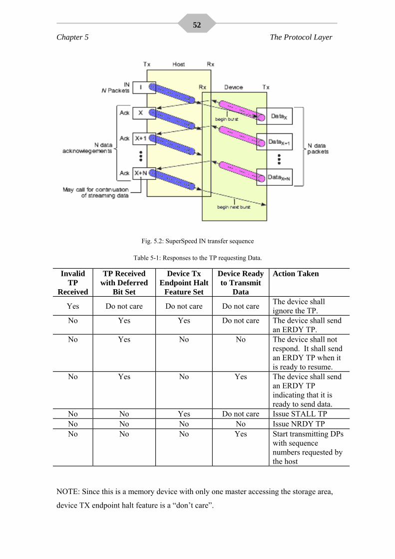
Chapter 5 The Protocol Layer
52
Fig. 5.2: SuperSpeed IN transfer sequence
Table 5-1: Responses to the TP requesting Data.
Invalid TP
Received
TP Received with Deferred
Bit Set
Device Tx Endpoint Halt
Feature Set
Device Ready to Transmit
Data
Action Taken
Yes Do not care Do not care Do not care The device shall ignore the TP.
No Yes Yes Do not care The device shall send an ERDY TP.
No Yes No No The device shall not respond. It shall send an ERDY TP when it is ready to resume.
No Yes No Yes The device shall send an ERDY TP indicating that it is ready to send data.
No No Yes Do not care Issue STALL TP No No No No Issue NRDY TP No No No Yes Start transmitting DPs
with sequence numbers requested by the host
NOTE: Since this is a memory device with only one master accessing the storage area,
device TX endpoint halt feature is a “don’t care”.

Chapter 5 The Protocol Layer
53
5.3.4.2 OUT Transfer During this transfer, host sources the data packets while device end point consumes
them.
Table 5-2: Host responses to the DP it receives from the device.
DPH has Invalid Values
Data Packet Payload Error
Host Can Accept Data
TP Returned by Host
Yes Do not care Do not care Discard data and do not send any TP. No Yes Do not care Discard data and send an ACK TP with
the Retry bit set requesting for one or more DPs with the Sequence Number field set to the sequence number of the DP that was corrupted.
No No No Discard data; send an ACK TP with the Retry bit set requesting for one or more DPs with the Sequence Number field set to the sequence number of the DP that the host was unable to receive. The ACK TP shall have the Host Error bit set to one to indicate that the host was unable to accept the data.
No No Yes Accept data and send an ACK TP requesting for zero or more DPs with the Sequence Number field set to the sequence number of the next DP expected. This is also an implicit acknowledgement that this DP was received successfully.
Each DP is acknowledged by the device having specified sequence number. Since the
device is capable of supporting data bursting of maximum burst size of four, the host
can send up to four DP before it waits for an ACK TP for the first DP it sent. DP
packets during OUT transfers are fetched from the dual-port-memory-bank-2, their
header information is extracted by the packet disassembler and if the packet received
was valid DP with no crc-32 errors is written into the SRAM. Header information is
provided to the protocol layer controller to provide appropriate response as given in the
table 5-3.

Chapter 5 The Protocol Layer
54
Table 5-3: Device responses to the DP received from the host.
DPH has
Invalid Values
DPH has Deferred Bit Set
Receiver Halt
Feature Set
Data Packet
Payload Error
Device Can Accept Data
TP Returned by Device
Yes Do not care
Do not care
Do not care Do not care Discard DP.
No Yes Yes Do not care
Do not care The device shall send an ERDY TP.
No Yes No Do not care
No The device shall not respond. It shall send an ERDY TP when it is ready to resume.
No Yes No Do not care
Yes The device shall send an ERDY TP.
No No Yes Do not care
Do not care The device shall send a STALL TP.
No No No Do not care No Discard DP, send an
NRDY TP.
No
No
No
Yes
Yes
Discard DP, send an ACK TP with the sequence number of the DP expected (thereby indicating that the DP was not received), the Retry bit set and the number of DPs that the device can receive for this endpoint.
No
No
No
No
Yes
Send an ACK TP indicating the sequence number of the next DP expected (thereby indicating that this DP was received successfully) and the number of DPs that the device can receive for this endpoint.
NOTE: Conditions for DPH to have deferred bit set or receiver halt feature are “don’t
care”.

Chapter 5 The Protocol Layer
55
Fig. 5.3: SuperSpeed OUT transfer sequence
5.3.5 Buffers for packet storage
Since the implemented USB3.0 device is capable of supporting burst transaction of
maximum burst size of four, protocol layer is implemented to have four data-packet
buffers for OUT transactions. This is rather accomplished in the SRAM entity because
intended system has nothing to do with the USB device operation. Nevertheless, in the
intended system there would be another dual-port-memory-bank serving as temporary
storage buffers and these buffers would be dumped into the hard-drive when they are
acknowledged.
5.3.6 Buffer controllers (buffer interfaces)
These controllers are meant for fetching and writing packets of specified data packet size on
temporary storage buffers in the device’s protocol layer or in dual‐port‐memory‐banks. The
concept behind these controllers is to remove the burden from the protocol layer controller
for fetching and writing the packets in the buffer storage area. They provide efficient
handshaking signal for efficient performance. Data is fetched from the buffers via read buffer
interfaces while written via write buffer interfaces.

Chapter # 6
The Master Controller

Chapter 6 The Master Controller
57
6.1 Master Controller Overview
Master Controller is developed to command the communication flow between each
module. The centralized master controller monitors and controls the decoding and
encoding operation separately. Fig. 6.1 depicts the IO interface of master controller with
LTSSM, Physical Layer, Link Layer and Protocol Layer Controllers.
Fig. 6.1: Top Level Block Diagram of Master Controller; showing IO interface with each layer and LTSSM.
The control flow for encoding and decoding processes are described in the following
sections.

Chapter 6 The Master Controller
58
6.2 Decoding Path Controller
The decoding process is to take packet from the Phy chip and pass it to link layer
controller (decoder) and so forth. Master controller follows the protocols in the
sequence mentioned below.
1. When Phy Layer controller (Phy decoder) receives the complete packet, it
generates an indication signal to master controller which in turn will initialize
the Link Layer (LL) decoder, provided that LL decoder is not already in a busy
state. Meanwhile, master also sends the packet size to the LL decoder; it had
received from the Phy Layer decoder at the complete reception of packet.
2. When the packet is processed by the LL decoder, it generates an indication
signal to master controller which in turn will initialize the Protocol Layer (PL)
decoder, provided that it is not already busy. Link layer decoder de-assembles
the packet received (Chapter 2) and sends the new packet size (packet size
changes after passing through the packet de-assembler) to master controller.
Master then sends this new packet size to protocol layer decoder at the time of
its initialization.
Note: Master must deassert the initializing signal of Link Layer and Protocol Layer
decoders as soon as they acknowledged.
Fig. 6.2 depicts the timing diagram of decoding process.

Chapter 6 The Master Controller
59

Chapter 6 The Master Controller
60
6.3 Encoding Path Controller
The controlling protocols, mentioned below, are followed by the master controller in
order to encode the packet
1. Protocol Layer (PL) Encoder is initialized when master-configuration valid
signal is received by the Master controller provided that the PL encoder must not
already busy. As soon as the complete packet is encoded, PL encoder generates
a “pl_enc_done” signal (shown in Fig. 6.3) to the master informing it the packet
has been transferred into the buffer and ready to be fetched by Link Layer
controller. Master controller then generates a signal to initialize the Link Layer
(LL) encoder, provided that LL encoder is not already in a busy state.
Meanwhile, master also sends the packet size to the Link Layer encoder; it had
received from the PL encoder at the complete reception of packet.
2. After processing, assembling and transferring the complete packet in the buffer
(Chapter #2), LL encoder generates an indication signal to master controller
which in turn will initialize the Phy Layer encoder, provided that it is not already
busy. Link layer encoder also sends the new packet size (packet size changes
after passing through the packet assembler) to master controller. Master then
sends this new packet size to Phy layer encoder at the time of its initialization.
Note: Master must deassert the initializing signal of Protocol Layer, Link Layer and Phy
Layer Encoders as soon as they acknowledged.
Fig. 6.3 depicts the timing diagram of encoding process.
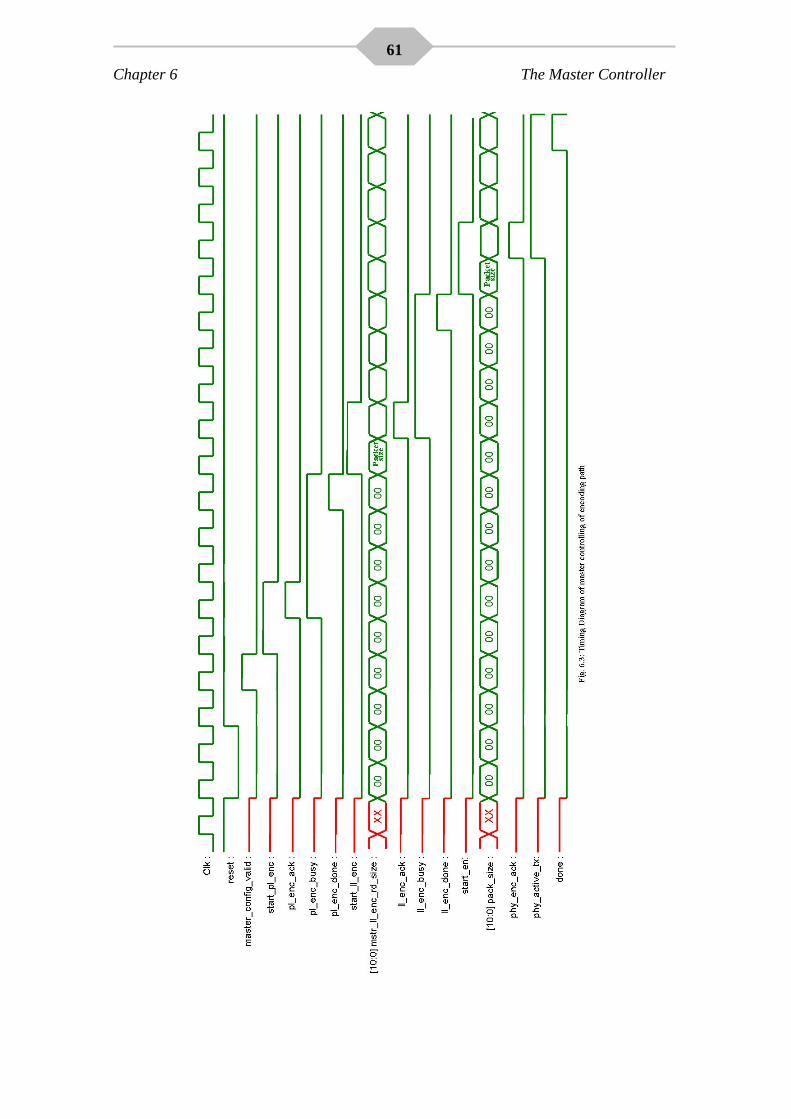
Chapter 6 The Master Controller
61

Chapter # 7
Functional Simulation of Implemented Device

63 Chapter 7 Functional Simulation of
Implemented Device
Simulation of the memory device is shown by looping back the data from the SRAM. In
the first phase of simulation, SRAM is completely filled with data sent from the
behavioral of host. In the second phase, the behavioral reads the filled SRAM and
checks whether the correct data is fetched. In this way operation from the PHY
controller, link layer up to protocol layer is verified. To meet this goal, several
compulsory features of each layer are also checked and verified.
7.1 Functional Verification of LTSSM
In order to prepare the device to handle data transmission and reception the links must
be initialized and trained. This process starts with the detection of a link partner at the
far end of the link in the RX.DETCT state. The detection starts as soon as the partner is
plugged in to the bus. Once the far end receiver detection is complete, the LTSSM then
starts training the link for synchronizing with the clock frequency and bit locking, in the
POLLING state, with the transmission and exchanging of TSEQ, TS1 and TS2. These
training sequences contain data bits that are designed to train and align the receivers of
two link partners. First of all TSEQ is sent for a specified number of times, then TS1
sequences are sent and received as well since the far end partner is also designed to
detect and send back these sequences. Upon a successful handshake of all these link
training stages between the link partners, the link is then brought to the active power
state, the U0 state, where it is ready to carry out all super speed data transmissions and
receptions.
7.2 Functional Verification of Phy Layer Controller
Phy decoder will play its role during the first phase of simulation as the data is coming
from the host. Phy decoder will remain idle unless RxValid signal (from behavioral of
Host, Fig. 2.2) is seen asserted. As soon as the rising edge of RxValid signal is sensed,
decoder requests Write Buffer Interface to received data coming from the Host. As soon
as it acknowledges, the Phy decoders starts fetching the data and place it on the ports
facing write buffer interface which in turn place the data into the buffer # 4 (Fig. 1.1).
Meanwhile it also looks for the control bytes (on RxData bus) on the basis of which it
could find out the size of packet (See Section 2.6). The operation of Phy encoder and
decoder are described in detail in sections 2.5 and 2.6, respectively.
64 Chapter 7 Functional Simulation of
Implemented Device
7.3 Functional Verification of Link Layer
When Link layer initializes to U0 it starts with the advertisement of last acknowledged
Header Sequence Number and Buffer Credit to its link partner. After advertisement link
layer starts sending LUP to its link partner until no transaction is carried out on encode
and decode path. When encode path initializes and protocol layer places the assembled
data to the dual port memory bank 1, link layer controller fetches the data and places the
link control word and already prepared and framed link commands of RX and TX with
the data and writes the encoded data on dual port memory bank-3 for PHY layer
,similarly when decode path initializes link layer reads the data from dual port memory
bank 4 and tests the data for CRC errors and matches the Header Sequence Number and
generate link command words and also decode the received link commands from link
partner and updates the parameter accordingly, reception of LBAD stops the transaction
of data unless LRTY is received or transmitted from link partners. Link commands for
Link power management are only accepted if all the header and data packets have been
acknowledged from link partners and removed from the buffers but
LGO_U3(requesting entry to U3) from host cannot be rejected.
7.4 Functional Verification of Protocol Layer
Master controller strobes protocol layer dis-assembler to initiate its operation. Protocol
layer dis-assembler decodes packet stored in the dual-port-memory bank # 3 extracts the
descriptions stored in the packet and route them towards the protocol layer controller
which decides about the packet to be sent in response, evaluates its configurations and
provides them to the protocol layer packet assembler while indicating the master
controller that packet assembler has valid configuration to initiate a valid packet. Master
controller then strobes the packet assembler which fetches required amount of data from
the SRAM along with its crc32 field (if it is an IN transaction) appends it with the
header packet thus assembling the packet and writing it into the dual-port-memory-bank
# 1. This is the most basic state machine of the protocol layer. Depending upon the
configurations fetched from the packets decoded and the packet assembled, protocol
layer either resumes the transaction with successive sequence numbers or wait for new
packet to be decoded. However, protocol layer assembler and protocol layer dis-
assembler works concurrently.

Bibliography
[1]. Universal Serial Bus 3.0 Specification, Revision 1.0, November 12, 2008.
[2]. Universal Serial Bus Specification, Revision 2.0, April 27, 2000.
[3]. PHY Interface for the PCI Express TM and USB Architectures, Version 2.90, Intel Corporation,
2007-08.
[4]. On-The-Go Supplement to the USB 2.0 Specification, Revision 1.3, December 5, 2006.
[5]. Inter-Chip USB Supplement to the USB 2.0 Specification, Revision 1.0, March 13, 2006.
[6]. High-Speed Inter-Chip USB Electrical Specification, Version 1.0, September 23, 2007.
[7]. UTMI+ Low Pin Interface (ULPI) Specification, Revision 1.1, October 20, 2004.
[8]. UTMI+ Specification, Revision 1.0, February 25, 2004.
[9]. USB System Architecture (USB 2.0), MindShare, Inc., Don Anderson.
[10]. Samir Palnitkar, Verilog HDL: A guide to Digital Design and Synthesis, Second Edition, Prentice
Hall, 2003.
[11]. Pong P. Chu, FPGA Prototyping by Verilog Examples, John Wiley & Sons, Inc., 2008.
[12]. Janick Bergeron, Writing Testbenches: Functional Verification of HDL Models.
[13]. Peter J. Ashenden, Digital Design: An Embedded System Approach using Verilog, Elsevier, 2008.