verilog foundation express with verilog hdl … reference...• chapter 1, “foundation express...
TRANSCRIPT
Verilog Reference Guide Printed in U.S.A.
Verilog Reference Guide
Foundation Express with Verilog HDL
Description Styles
Structural Descriptions
Expressions
Functional Descriptions
Register and Three-State Inference
Foundation Express Directives
Writing Circuit Descriptions
Verilog Syntax
Appendix A—Examples

Verilog Reference Guide
The Xilinx logo shown above is a registered trademark of Xilinx, Inc.
FPGA Architect, FPGA Foundry, NeoCAD, NeoCAD EPIC, NeoCAD PRISM, NeoROUTE, Timing Wizard, TRACE,XACT, XILINX, XC2064, XC3090, XC4005, XC5210, and XC-DS501 are registered trademarks of Xilinx, Inc.
The shadow X shown above is a trademark of Xilinx, Inc.
All XC-prefix product designations, A.K.A. Speed, Alliance Series, AllianceCORE, BITA, CLC, Configurable LogicCell, CORE Generator, CoreGenerator, CoreLINX, Dual Block, EZTag, FastCLK, FastCONNECT, FastFLASH,FastMap, Foundation, HardWire, LCA, LogiBLOX, Logic Cell, LogiCORE, LogicProfessor, MicroVia, PLUSASM,PowerGuide, PowerMaze, QPro, RealPCI, RealPCI 64/66, SelectI/O, Select-RAM, Select-RAM+, Smartguide,Smart-IP, SmartSearch, Smartspec, SMARTSwitch, Spartan, TrueMap, UIM, VectorMaze, VersaBlock,VersaRing, Virtex, WebLINX, XABEL, XACTstep, XACTstep Advanced, XACTstep Foundry, XACT-Floorplanner,XACT-Performance, XAM, XAPP, X-BLOX, X-BLOX plus, XChecker, XDM, XDS, XEPLD, Xilinx FoundationSeries, XPP, XSI, and ZERO+ are trademarks of Xilinx, Inc. The Programmable Logic Company and TheProgrammable Gate Array Company are service marks of Xilinx, Inc.
All other trademarks are the property of their respective owners.
Xilinx, Inc. does not assume any liability arising out of the application or use of any product described or shownherein; nor does it convey any license under its patents, copyrights, or maskwork rights or any rights of others.Xilinx, Inc. reserves the right to make changes, at any time, in order to improve reliability, function or design andto supply the best product possible. Xilinx, Inc. will not assume responsibility for the use of any circuitry describedherein other than circuitry entirely embodied in its products. Xilinx, Inc. devices and products are protected underone or more of the following U.S. Patents: 4,642,487; 4,695,740; 4,706,216; 4,713,557; 4,746,822; 4,750,155;4,758,985; 4,820,937; 4,821,233; 4,835,418; 4,855,619; 4,855,669; 4,902,910; 4,940,909; 4,967,107; 5,012,135;5,023,606; 5,028,821; 5,047,710; 5,068,603; 5,140,193; 5,148,390; 5,155,432; 5,166,858; 5,224,056; 5,243,238;5,245,277; 5,267,187; 5,291,079; 5,295,090; 5,302,866; 5,319,252; 5,319,254; 5,321,704; 5,329,174; 5,329,181;5,331,220; 5,331,226; 5,332,929; 5,337,255; 5,343,406; 5,349,248; 5,349,249; 5,349,250; 5,349,691; 5,357,153;5,360,747; 5,361,229; 5,362,999; 5,365,125; 5,367,207; 5,386,154; 5,394,104; 5,399,924; 5,399,925; 5,410,189;5,410,194; 5,414,377; 5,422,833; 5,426,378; 5,426,379; 5,430,687; 5,432,719; 5,448,181; 5,448,493; 5,450,021;5,450,022; 5,453,706; 5,455,525; 5,466,117; 5,469,003; 5,475,253; 5,477,414; 5,481,206; 5,483,478; 5,486,707;5,486,776; 5,488,316; 5,489,858; 5,489,866; 5,491,353; 5,495,196; 5,498,979; 5,498,989; 5,499,192; 5,500,608;5,500,609; 5,502,000; 5,502,440; 5,504,439; 5,506,518; 5,506,523; 5,506,878; 5,513,124; 5,517,135; 5,521,835;5,521,837; 5,523,963; 5,523,971; 5,524,097; 5,526,322; 5,528,169; 5,528,176; 5,530,378; 5,530,384; 5,546,018;5,550,839; 5,550,843; 5,552,722; 5,553,001; 5,559,751; 5,561,367; 5,561,629; 5,561,631; 5,563,527; 5,563,528;5,563,529; 5,563,827; 5,565,792; 5,566,123; 5,570,051; 5,574,634; 5,574,655; 5,578,946; 5,581,198; 5,581,199;5,581,738; 5,583,450; 5,583,452; 5,592,105; 5,594,367; 5,598,424; 5,600,263; 5,600,264; 5,600,271; 5,600,597;5,608,342; 5,610,536; 5,610,790; 5,610,829; 5,612,633; 5,617,021; 5,617,041; 5,617,327; 5,617,573; 5,623,387;5,627,480; 5,629,637; 5,629,886; 5,631,577; 5,631,583; 5,635,851; 5,636,368; 5,640,106; 5,642,058; 5,646,545;5,646,547; 5,646,564; 5,646,903; 5,648,732; 5,648,913; 5,650,672; 5,650,946; 5,652,904; 5,654,631; 5,656,950;5,657,290; 5,659,484; 5,661,660; 5,661,685; 5,670,896; 5,670,897; 5,672,966; 5,673,198; 5,675,262; 5,675,270;5,675,589; 5,677,638; 5,682,107; 5,689,133; 5,689,516; 5,691,907; 5,691,912; 5,694,047; 5,694,056; 5,724,276;5,694,399; 5,696,454; 5,701,091; 5,701,441; 5,703,759; 5,705,932; 5,705,938; 5,708,597; 5,712,579; 5,715,197;5,717,340; 5,719,506; 5,719,507; 5,724,276; 5,726,484; 5,726,584; 5,734,866; 5,734,868; 5,737,234; 5,737,235;5,737,631; 5,742,178; 5,742,531; 5,744,974; 5,744,979; 5,744,995; 5,748,942; 5,748,979; 5,752,006; 5,752,035;5,754,459; 5,758,192; 5,760,603; 5,760,604; 5,760,607; 5,761,483; 5,764,076; 5,764,534; 5,764,564; 5,768,179;5,770,951; 5,773,993; 5,778,439; 5,781,756; 5,784,313; 5,784,577; 5,786,240; 5,787,007; 5,789,938; 5,790,479;
R
Xilinx Development System

5,790,882; 5,795,068; 5,796,269; 5,798,656; 5,801,546; 5,801,547; 5,801,548; 5,811,985; 5,815,004; 5,815,016;5,815,404; 5,815,405; 5,818,255; 5,818,730; 5,821,772; 5,821,774; 5,825,202; 5,825,662; 5,825,787; 5,828,230;5,828,231; 5,828,236; 5,828,608; 5,831,448; 5,831,460; 5,831,845; 5,831,907; 5,835,402; 5,838,167; 5,838,901;5,838,954; 5,841,296; 5,841,867; 5,844,422; 5,844,424; 5,844,829; 5,844,844; 5,847,577; 5,847,579; 5,847,580;5,847,993; 5,852,323; Re. 34,363, Re. 34,444, and Re. 34,808. Other U.S. and foreign patents pending. Xilinx,Inc. does not represent that devices shown or products described herein are free from patent infringement or fromany other third party right. Xilinx, Inc. assumes no obligation to correct any errors contained herein or to adviseany user of this text of any correction if such be made. Xilinx, Inc. will not assume any liability for the accuracy orcorrectness of any engineering or software support or assistance provided to a user.
Xilinx products are not intended for use in life support appliances, devices, or systems. Use of a Xilinx product insuch applications without the written consent of the appropriate Xilinx officer is prohibited.
Copyright 1991-1999 Xilinx, Inc. All Rights Reserved.
Verilog Reference Guide

Verilog Reference Guide
Xilinx Development System

About This Manual
This manual describes how to use the Xilinx Foundation Express program to translate and optimize a Verilog HDL description into an internal gate-level equivalent.
Before using this manual, you should be familiar with the operations that are common to all Xilinx software tools. These operations are covered in the Quick Start Guide.
For additional information, go to http://support.xilinx.com. The following table lists some of the resources you can access from this page. You can also directly access some of these resources using the provided URLs.
Resource Description/URL
Tutorial Tutorials covering Xilinx design flows, from design entry to verification and debugginghttp://support.xilinx.com/support/techsup/tutorials/index.htm
AnswersDatabase
Current listing of solution records for the Xilinx software toolsSearch this database using the search function at http://support.xilinx.com/support/searchtd.htm
Application Notes
Descriptions of device-specific design techniques and approacheshttp://support.xilinx.com/apps/appsweb.htm
Data Book Pages from The Programmable Logic Data Book, which describe device-specific information on Xilinx device characteristics, including read-back, boundary scan, configuration, length count, and debugginghttp://support.xilinx.com/partinfo/databook.htm
Verilog Reference Guide v

Verilog Reference Guide
Manual ContentsThis manual covers the following topics.
• Chapter 1, “Foundation Express with Verilog HDL,” discusses general concepts about Verilog and the Foundation Express design process and methodology.
• Chapter 2, “Description Styles,” presents the concepts you need to make the necessary architectural decisions and use the constructs best suited for synthesis.
• Chapter 3, “Structural Descriptions,” discusses modules and module instantiations.
• Chapter 4, “Expressions,” explains how to build and use expres-sions with constant-valued expressions, operators, operands, and expression bit-widths.
• Chapter 5, “Functional Descriptions,” describes the construction and use of functional descriptions. Task statements and always blocks are also discussed.
• Chapter 6, “Register and Three-State Inference,” describes how to report inference results, control inference behavior, and infer cells.
• Chapter 7, “Foundation Express Directives” describes Founda-tion Express directives and their effect on translation.
• Chapter 8, “Writing Circuit Descriptions” describes how to write a Verilog description to ensure an efficient implementation.
• Chapter 9, “Verilog Syntax,” contains syntax descriptions of the Verilog language as supported by Foundation Express.
• Appendix A, “Examples,” presents examples that demonstrate basic concepts of Foundation Express.
Xcell Journals Quarterly journals for Xilinx programmable logic usershttp://support.xilinx.com/xcell/xcell.htm
Tech Tips Latest news, design tips, and patch information on the Xilinx design environmenthttp://support.xilinx.com/support/techsup/journals/index.htm
Resource Description/URL
vi Xilinx Development System

Conventions
This manual uses the following typographical and online document conventions. An example illustrates each typographical convention.
TypographicalThe following conventions are used for all documents.
• Courier font indicates messages, prompts, and program files that the system displays.
speed grade: -100
• Courier bold indicates literal commands that you enter in a syntactical statement. However, braces “{ }” in Courier bold are not literal and square brackets “[ ]” in Courier bold are literal only in the case of bus specifications, such as bus [7:0].
rpt_del_net=
Courier bold also indicates commands that you select from a menu.
File → Open
• Italic font denotes the following items.
• Variables in a syntax statement for which you must supply values
edif2ngd design_name
• References to other manuals
See the Development System Reference Guide for more informa-tion.
Verilog Reference Guide vii

Verilog Reference Guide
• Emphasis in text
If a wire is drawn so that it overlaps the pin of a symbol, the two nets are not connected.
• Square brackets “[ ]” indicate an optional entry or parameter. However, in bus specifications, such as bus [7:0], they are required.
edif2ngd [option_name] design_name
• Braces “{ }” enclose a list of items from which you must choose one or more.
lowpwr ={on|off}
• A vertical bar “|” separates items in a list of choices.
lowpwr ={on|off}
• A vertical ellipsis indicates repetitive material that has been omitted.
IOB #1: Name = QOUT’IOB #2: Name = CLKIN’...
• A horizontal ellipsis “. . .” indicates that an item can be repeated one or more times.
allow block block_name loc1 loc2 ... locn;
Online DocumentThe following conventions are used for online documents.
• Red-underlined text indicates an interbook link, which is a cross-reference to another book. Click the red-underlined text to open the specified cross-reference.
• Blue-underlined text indicates an intrabook link, which is a cross-reference within a book. Click the blue-underlined text to open the specified cross-reference.
viii Xilinx Development System

Contents
About This ManualManual Contents ............................................................................ vi
ConventionsTypographical................................................................................. viiOnline Document ........................................................................... viii
Chapter 1 Foundation Express with Verilog HDL
Hardware Description Languages.................................................. 1-1Foundation Express Design Process ............................................. 1-2Using Foundation to Compile a Verilog HDL Design ..................... 1-3Design Methodology ...................................................................... 1-4
Chapter 2 Description Styles
Design Hierarchy............................................................................ 2-2Structural Descriptions ................................................................... 2-2Functional Descriptions.................................................................. 2-3Mixing Structural and Functional Descriptions ............................... 2-3Register Selection .......................................................................... 2-6
Register Instantiation ................................................................ 2-6Register Inference..................................................................... 2-6
Asynchronous Designs .................................................................. 2-7
Chapter 3 Structural Descriptions
Modules.......................................................................................... 3-1Macromodules................................................................................ 3-2Port Definitions............................................................................... 3-3Port Names .................................................................................... 3-4
Renaming Ports ........................................................................ 3-4Module Statements and Constructs ............................................... 3-5
Verilog Reference Guide ix

Verilog Reference Guide
Structural Data Types ............................................................... 3-6parameter ............................................................................ 3-6wire ...................................................................................... 3-7wand .................................................................................... 3-8wor ....................................................................................... 3-8tri.......................................................................................... 3-8supply0 and supply1 ............................................................ 3-9reg........................................................................................ 3-9
Port Declarations ...................................................................... 3-10input ..................................................................................... 3-10output................................................................................... 3-10inout ..................................................................................... 3-11
Continuous Assignment ............................................................ 3-11Module Instantiations ..................................................................... 3-12
Named and Positional Notation ................................................ 3-13Parameterized Designs............................................................. 3-14Gate-Level Modeling................................................................. 3-14Three-State Buffer Instantiation ................................................ 3-15
Chapter 4 Expressions
Constant-Valued Expressions........................................................ 4-1Operators ....................................................................................... 4-2
Arithmetic Operators ................................................................. 4-3Relational Operators ................................................................. 4-4Equality Operators .................................................................... 4-4Handling Comparisons to X or Z............................................... 4-5Logical Operators...................................................................... 4-6Bit-wise Operators .................................................................... 4-7Reduction Operators................................................................. 4-7Shift Operators.......................................................................... 4-8Conditional Operator................................................................. 4-8Concatenation Operator............................................................ 4-9Operator Precedence................................................................ 4-10
Operands ....................................................................................... 4-11Numbers ................................................................................... 4-11Wires and Registers.................................................................. 4-11
Bit-Selects............................................................................ 4-12Part-Selects ......................................................................... 4-12
Function Calls ........................................................................... 4-12Concatenation of Operands ...................................................... 4-13
Expression Bit Widths .................................................................... 4-13
x Xilinx Development System

Contents
Chapter 5 Functional Descriptions
Sequential Constructs .................................................................... 5-1Function Declarations .................................................................... 5-2
Input Declarations ..................................................................... 5-3Function Output ........................................................................ 5-4Register Declarations................................................................ 5-4Memory Declarations ................................................................ 5-5Parameter Declarations ............................................................ 5-5Integer Declarations.................................................................. 5-6
Function Statements ...................................................................... 5-6Procedural Assignments ........................................................... 5-7RTL Assignments...................................................................... 5-7begin...end Block Statements ................................................... 5-10if...else Statements ................................................................... 5-11Conditional Assignments .......................................................... 5-12case Statements ....................................................................... 5-13Full Case and Parallel Case ..................................................... 5-14casex Statements ..................................................................... 5-16casez Statements ..................................................................... 5-17for Loops ................................................................................... 5-19while Loops ............................................................................... 5-20forever Loops ............................................................................ 5-21disable Statements ................................................................... 5-21
task Statements ............................................................................. 5-22always Blocks................................................................................. 5-23
Event Expression ...................................................................... 5-24Incomplete Event Specification................................................. 5-25
Chapter 6 Register and Three-State Inference
Register Inference.......................................................................... 6-1The Inference Report ................................................................ 6-1Latch Inference Warnings ......................................................... 6-2Controlling Register Inference .................................................. 6-3Inferring Latches ....................................................................... 6-5
Inferring SR Latches ............................................................ 6-5Inferring D Latches .............................................................. 6-6Simple D Latch ................................................................... 6-8D Latch with Asynchronous Set or Reset ........................... 6-9D Latch with Asynchronous Set and Reset ........................ 6-12Understanding the Limitations of D Latch Inference............ 6-13Inferring Master-Slave Latches............................................ 6-13
Verilog Reference Guide xi
Verilog Reference Guide
Inferring Flip-Flops .................................................................... 6-14Inferring D Flip-Flops ........................................................... 6-14Simple D Flip-Flop .............................................................. 6-15D Flip-Flop with Asynchronous Set or Reset ...................... 6-17D Flip-Flop with Asynchronous Set and Reset ................... 6-19D Flip-Flop with Synchronous Set or Reset ........................ 6-20D Flip-Flop with Synchronous and Asynchronous Load ..... 6-22Multiple Flip-Flops with Asynchronous and Synchronous Controls 6-24Understanding the Limitations of D Flip-Flop Inference....... 6-26Inferring JK Flip-Flops.......................................................... 6-28JK Flip-Flop ......................................................................... 6-28JK Flip-Flop With Asynchronous Set and Reset ................. 6-29Inferring Toggle Flip-Flops................................................... 6-31Toggle Flip-Flop With Asynchronous Set or Reset ............. 6-31Toggle Flip-Flop With Enable and Asynchronous Reset .... 6-33Getting the Best Results ...................................................... 6-34Minimizing Flip-Flop Count .................................................. 6-35Correlating with Simulation Results ..................................... 6-36
Understanding Limitations of Register Inference ...................... 6-37Three-State Inference .................................................................... 6-38
Reporting Three-State Inference .............................................. 6-38Controlling Three-State Inference............................................. 6-38Inferring Three-State Drivers .................................................... 6-38
Simple Three-State Driver ................................................... 6-39Registered Three-State Drivers ........................................... 6-42
Understanding the Limitations of Three-State Inference .......... 6-44
Chapter 7 Foundation Express Directives
Notation for Foundation Express Directives................................... 7-1translate_off and translate_on Directives....................................... 7-2parallel_case Directive ................................................................... 7-3full_case Directive .......................................................................... 7-4state_vector Directive..................................................................... 7-6enum Directive ............................................................................... 7-7Component Implication .................................................................. 7-12
Chapter 8 Writing Circuit Descriptions
How Statements Are Mapped to Logic........................................... 8-1Design Structure ....................................................................... 8-2Using Design Knowledge.......................................................... 8-5
xii Xilinx Development System
Contents
Optimizing Arithmetic Expressions ........................................... 8-5Arranging Expression Trees for Minimum Delay ................. 8-5Considering Signal Arrival Times ........................................ 8-6Using Parentheses ............................................................. 8-7Considering Overflow Characteristics ................................. 8-8Sharing Common Subexpressions ...................................... 8-9
Using Operator Bit-Width Efficiently.......................................... 8-11Using State Information ............................................................ 8-12Describing State Machines ....................................................... 8-14Minimizing Registers................................................................. 8-18Separating Sequential and Combinatorial Assignments........... 8-20
Don’t Care Inference ...................................................................... 8-22Limitations of Using Don’t Care Values .................................... 8-22Differences Between Simulation and Synthesis ....................... 8-23
Propagating Constants................................................................... 8-24Synthesis Issues ............................................................................ 8-24
Feedback Paths and Latches ................................................... 8-24Synthesizing Asynchronous Designs........................................ 8-24
Designing for Overall Efficiency ..................................................... 8-26Describing Random Logic......................................................... 8-26Sharing Complex Operators ..................................................... 8-27
Chapter 9 Verilog Syntax
Syntax ............................................................................................ 9-1BNF Syntax Formalism ............................................................. 9-1BNF Syntax............................................................................... 9-2
Lexical Conventions ....................................................................... 9-11White Space.............................................................................. 9-11Comments................................................................................. 9-12Numbers ................................................................................... 9-12Identifiers .................................................................................. 9-13Operators .................................................................................. 9-14Macro Substitution .................................................................... 9-14Include Construct ...................................................................... 9-14Simulation Directives ................................................................ 9-15Verilog System Functions ......................................................... 9-16
Verilog Keywords ........................................................................... 9-17Unsupported Verilog Language Constructs ................................... 9-18
Unsupported Definitions and Declaration ................................. 9-18Unsupported Statements .......................................................... 9-18Unsupported Operators ............................................................ 9-19Unsupported Gate-Level Constructs......................................... 9-19
Verilog Reference Guide xiii

Verilog Reference Guide
Appendix A ExamplesCount Zeros—Combinatorial Version ............................................ A-1Count Zeros—Sequential Version.................................................. A-3Drink Machine—State Machine Version ........................................ A-6Drink Machine—Count Nickels Version ......................................... A-9Carry-Lookahead Adder................................................................. A-11
xiv Xilinx Development System

Chapter 1
Foundation Express with Verilog HDL
Foundation Express translates and optimizes a Verilog HDL descrip-tion into an internal gate-level equivalent, then compiles this repre-sentation to produce an optimized architecture-specific design in a given FPGA or CPLD technology.
This chapter introduces the main concepts and capabilities of Foun-dation Express in the following sections.
• “Hardware Description Languages”
• “Foundation Express Design Process”
• “Using Foundation to Compile a Verilog HDL Design”
• “Design Methodology”
Hardware Description LanguagesHardware description languages (HDLs) describe the architecture and behavior of discrete electronic systems. Modern HDLs and their associated simulators are very powerful tools for integrated circuit designers.
A typical HDL supports a mixed-level description in which gate and netlist constructs are used with functional descriptions. This mixed-level capability enables you to describe system architectures at a very high level of abstraction, then incrementally refine a design’s detailed gate-level implementation.
HDL descriptions play an important role in modern design method-ology for three main reasons.
• You can verify design functionality early in the design process. A design written as an HDL description can be simulated immedi-ately. Design simulation at this higher level, before implementa-
Verilog Reference Guide 1-1
Verilog Reference Guide
tion at the gate-level, allows you to evaluate architectural and design decisions.
• Using Foundation Express to compile Verilog and synthesize logic, you can automatically convert an HDL description to a gate-level implementation in a target FPGA or CPLD technology. This step eliminates the former technology-specific design bottle-neck, the majority of circuit design time, and the errors intro-duced when you hand translate an HDL specification to gates.
• With Foundation Express logic optimization, you can automati-cally transform a synthesized design into a smaller or faster circuit. Foundation Express both synthesizes and optimizes logic. For further information, refer to the Foundation Express online help.
• An HDL description is more easily read and understood than a netlist or schematic description. HDL descriptions provide tech-nology independent documentation of a design and its function-ality. Because the initial HDL design description is technology independent, you can use it again to generate the design in a different technology, without having to translate it from the orig-inal technology.
Foundation Express Design ProcessFoundation Express translates Verilog language hardware descrip-tions to an internal design format. You can then use Foundation Express to optimize and map the design to a specific FPGA tech-nology library, as shown in the following figure.
1-2 Xilinx Development System

Foundation Express with Verilog HDL
.
Figure 1-1 Foundation Express Design Process
Foundation Express supports a majority of the Verilog constructs. For exceptions, see the “Unsupported Verilog Language Constructs” section of the “Verilog Syntax” chapter.
Using Foundation to Compile a Verilog HDL DesignWhen a Verilog design is read into Foundation Express, it is converted to an internal database format so that Foundation Express can synthesize and optimize the design. When Foundation Express optimizes a design, it may restructure part or all of the design. You control the degree of restructuring. You have the following options.
• Fully preserve a design’s hierarchy
• Combine certain modules with others
• Compress the entire design into one module (called flattening the design), if it is beneficial
The following section describes the design process that uses Founda-tion Express with a Verilog HDL simulator.
X8588
Verilog Description
OptimizedTechnology-Specific
Netlist
FPGA Technology Library Foundation Express
Verilog Reference Guide 1-3

Verilog Reference Guide
Design MethodologyThe figure below shows a typical design process that uses Founda-tion Express and a Verilog HDL simulator. Each step of this design model is described in detail after the figure.
Figure 1-2 Design Flow
X8589
1
2
4
Compare Outputs
5
63
7
Foundation Express
FPGA Development System
Verilog HDL SimulatorVerilog HDL Simulator
Verilog HDLDescription
VerilogTest Drivers
SimulationOutput
SimulationOutput
1-4 Xilinx Development System

Foundation Express with Verilog HDL
The following numbered steps correspond to the numbers in the figure above.
1. Write a design description in the Verilog language.
This description can be a combination of structural and func-tional elements (as shown in the “Description Styles” chapter). It is used with both Foundation Express and a Verilog simulator.
2. Write Verilog language test drivers for the Verilog HDL simu-lator.
The drivers supply test vectors for simulation and gather output data. For information on writing these drivers, see the appro-priate simulator manual.
3. Simulate the design by using a Verilog HDL simulator, and verify that the description is correct.
4. Synthesize and optimize the Verilog design description into a gate-level netlist using Foundation Express.
Foundation Express generates optimized netlists to satisfy timing constraints for a targeted FPGA architecture.
5. Map and, then, place and route the FPGA netlist using your FPGA development system. Generate a Verilog netlist for post-place and route simulation.
The development system includes simulation models and inter-faces required for the design flow.
6. Simulate the technology-specific version of the design with the Verilog simulator.
You can use the original Verilog simulation drivers from Step 3 because module and port definitions are preserved through the translation and optimization processes.
7. Compare the output of the gate-level simulation (Step 6) with the output of the original Verilog description simulation (Step 3) to verify that the implementation is correct.
Verilog Reference Guide 1-5

Verilog Reference Guide
1-6 Xilinx Development System

Chapter 2
Description Styles
A Verilog circuit description can be one of two types; a structural description or a functional description, also referred to as a Register Transfer Level (RTL) description. A structural description defines the exact physical makeup of the circuit, showing the details of the components and the connections between them. A functional or RTL description describes a circuit in terms of its registers and the combi-natorial logic between the registers.
The style of your initial Verilog description has a major effect on the characteristics of the resulting gate-level design synthesized by Foun-dation Express. The organization and style of a Verilog description determines the basic architecture of your design. Because Foundation Express automates most of the logic-level decisions required in your design, you can concentrate on architectural tradeoffs.
You can use Foundation Express to make some of the high-level architectural decisions. Certain Verilog constructs are well suited to synthesis. To make these decisions and use the constructs, you need to become familiar with the concepts covered in the following sections of this chapter.
• “Design Hierarchy”
• “Structural Descriptions”
• “Functional Descriptions”
• “Mixing Structural and Functional Descriptions”
• “Register Selection”
• “Asynchronous Designs”
Verilog Reference Guide 2-1

Verilog Reference Guide
Design HierarchyFoundation Express maintains the hierarchical boundaries you define when you use structural Verilog. These boundaries have two major effects.
• Each module you specify in your HDL description is synthesized separately and maintained as a distinct design. The constraints for the design are maintained, and you can optimize each module separately in Foundation Express.
• The modules that you instantiate within HDL descriptions are maintained during input. The instance name you assign to user-defined components is carried through to the gate-level implementation.
The “Structural Descriptions” chapter discusses modules and module instantiations.
Note: Foundation Express does not automatically maintain (create) the hierarchy of other nonstructural Verilog constructs such as blocks, loops, functions, and tasks. These elements of an HDL description are translated in the context of their design.
The choice of hierarchical boundaries has a significant effect on the quality of the synthesized design. You can optimize a design while preserving these hierarchical boundaries using Foundation Express. However, Foundation Express only partially optimizes logic across hierarchical modules. Full optimization is possible across those parts of the design hierarchy that are collapsed in Foundation Express.
Structural DescriptionsThe structural elements of a Verilog description consist of generic logic gates, library-specific components, and user-defined compo-nents connected by wires. In one way, a structural description can be viewed as a simple netlist composed of nets that connect instantia-tions of gates. However, unlike a netlist, nets in the structural description can be driven by an arbitrary expression that describes the value assigned to the net. A statement that drives an arbitrary expression onto a net is called a continuous assignment. Continuous assignments are convenient links between pure netlist descriptions and functional descriptions.
2-2 Xilinx Development System
Description Styles
A Verilog structural description can define a range of hierarchical and gate-level constructs, including module definitions, module instantiations, and netlist connections. Refer to the “Structural Descriptions” chapter for more information.
Functional DescriptionsThe functional elements of a Verilog description consist of function declarations, task statements, and always blocks. These elements describe the function of the circuit but do not describe its physical makeup or layout. The choice of gates and components is left entirely to Foundation Express.
You can construct functional descriptions with the Verilog functional constructs described in the “Functional Descriptions” chapter. These constructs can appear within functions or always blocks. Functions imply only combinatorial logic; always blocks can imply either combinatorial or sequential logic.
Although many Verilog functional constructs appear sequential in nature (for example, for loops and multiple assignments to the same variable), these constructs describe combinatorial logic networks. Other functional constructs imply sequential logic networks. Latches and registers are inferred from these constructs. Refer to the “Register and Three-State Inference” chapter.
Mixing Structural and Functional DescriptionsWhen you use a functional description style in a design, you typically describe the combinatorial portions of a design in Verilog functions, always blocks, and assignments. The complexity of the logic deter-mines whether you use one or many functions.
The example “Mixed Structural and Functional Descriptions” shows how structural and functional description styles are mixed in a design specification. In this example, the function detect_logic deter-mines whether the input bit is a 0 or a 1. After making this determina-tion, detect_logic sets ns to the next state of the machine. An always block infers flip-flops to hold the state information between clock cycles.
You can directly specify elements of a design as module instantia-tions at the structural level. For example, see the three-state buffer, t1,
Verilog Reference Guide 2-3

Verilog Reference Guide
in the following example of mixed structural and functional descrip-tions.
Note: The three-state buffers can be inferred. For more information, refer to the “Three-State Inference” section of the “Register and Three-State Inference” chapter.)
You can also use this description style to identify the wires and ports that carry information from one part of the design to another.
// This finite state machine (Mealy type) reads one// bit per clock cycle and detects three or more// consecutive ones.module three_ones(signal,clock,detect,output_enable);input signal, clock, output_enable;output detect;
// Declare current state and next state variables.reg [1:0] cs;reg [1:0] ns;wire ungated_detect;
// declare the symbolic names for statesparameter NO_ONES=0,ONE_ONE=1,TWO_ONES=2
AT_LEAST_THREE_ONES=3;
// ************* STRUCTURAL DESCRIPTION *********** // Instance of a three-state gate that enables outputthree_state t1(ungated_detect,output_enable, detect);
// ***************** ALWAYS BLOCK **************** // always block infers flip-flops to hold the state of // the FSM.always @ (posedge clock) begin
cs = ns;end
// ************* FUNCTIONAL DESCRIPTION ************function detect_logic;
input [1:0] cs; input signal;begin
2-4 Xilinx Development System
Description Styles
detect_logic = 0; // default valueif ( signal == 0 ) // bit is zero
ns = NO_ONES;else // bit is one,increment state
case (cs)NO_ONES: ns = ONE_ONE;ONE_ONE: ns = TWO_ONES;TWO_ONES, AT_LEAST_THREE_ONES:
beginns = AT_LEAST_THREE_ONES;detect_logic = 1;
endendcase
endendfunction
// ************** assign STATEMENT **************assign ungated_detect = detect_logic( cs, signal );endmodule
To successfully synthesize a structural or functional HDL descrip-tion, the description must conform to the three elements of Verilog synthesis.
• Design methodology
Design methodology refers to the synthesis design process described in the “Foundation Express with Verilog HDL” chapter that uses Foundation Express and a Verilog HDL Simulator.
• Description style
Use the HDL design and coding style that makes the best use of the synthesis process to obtain high quality results from Founda-tion Express. See the “Writing Circuit Descriptions” chapter.
• Language constructs
The third component of the Verilog synthesis policy is the set of Verilog constructs that describes your design, determines its architecture, and gives consistently good results.
Foundation Express uses HDL constructs that maximize coding flexibility while producing consistently good results. Although Foundation Express can read the entire Verilog language, a few HDL constructs cannot be synthesized. These constructs are unsupported, because they cannot be realized in logic. For
Verilog Reference Guide 2-5

Verilog Reference Guide
example, you cannot use simulation time as a trigger, because time is an element of the simulation process and cannot be real-ized. See the “Unsupported Verilog Language Constructs” section of the “Verilog Syntax” chapter for unsupported Verilog constructs.
Register SelectionThe placement of registers and the clocking scheme are important architectural decisions. There are two ways to define registers in your Verilog description; instantiating or inferring registers. Each method has specific advantages and disadvantages.
Register InstantiationYou can directly instantiate registers into a Verilog description, selecting from any element in your FPGA or CPLD library. (Clocking schemes can be arbitrarily complex.) You can choose between a flip-flop or a latch-based architecture. The main disadvantages to this approach follow.
• The Verilog description is specific to a given technology, because you choose structural elements from that technology library. However, you can isolate that portion of your design with directly instantiated registers as a separate component (module), and, then, connect it to the rest of the design.
• The description is more difficult to write.
Register InferenceYou can use some Verilog constructs to direct Foundation Express to infer registers from the description. This method allows Foundation Express to select the type of component inferred, based on constraints. Therefore, if you need a specific component, you should instantiate registers, instead of inferring them. However, some types of registers and latches cannot be inferred.
The following advantages of inferring registers directly counter the disadvantages of instantiating registers.
• Inferring registers is technology independent.
• With register inference, the Verilog description is much easier to write.
2-6 Xilinx Development System

Description Styles
See the “Register Inference” section of the “Register and Three-State Inference” chapter for a discussion of latch and register inference.
Asynchronous DesignsYou can use Foundation Express to construct asynchronous designs that use multiple clocks or gated clocks. Although these designs are logically and statically correct, they may not simulate or operate correctly because of race conditions.
The “Foundation Express Directives” chapter describes how to write Verilog descriptions of asynchronous designs.
Verilog Reference Guide 2-7

Verilog Reference Guide
2-8 Xilinx Development System

Chapter 3
Structural Descriptions
A Verilog circuit description can be one of two types; a structural description or a functional description, also referred to as a Register Transfer Level (RTL) description. A structural description defines the exact physical makeup of the circuit, detailing components and the connections between them. A functional or RTL description describes a circuit in terms of its registers and the combinatorial logic between the registers.
This chapter describes the construction of structural descriptions and is divided into the following sections.
• “Modules”
• “Macromodules”
• “Port Definitions”
• “Module Statements and Constructs”
• “Module Instantiations”
ModulesThe principal design entity in the Verilog language is a module. A module consists of the module name, its input and output descrip-tion (port definition), a description of the functionality or implemen-tation for the module (module statements and constructs), and named instantiations. The basic structural parts of a module are illus-trated in the following figure.
Verilog Reference Guide 3-1

Verilog Reference Guide
Figure 3-1 Structural Parts of a Module
The following example shows a simple module that implements a 2-input NAND gate by instantiating an AND gate and an INV gate. The first line of the module definition declares the name of the module and a list of ports. The second and third lines declare the direction for all ports. (Ports are either inputs, outputs, or bidirec-tionals.) The fourth line in the description creates a wire variable.
The next two lines instantiate the two components, creating copies named instance1 and instance2 of the components AND and INV. These components connect to the ports of the module and are finally connected by using the variable and_out.
module NAND(a,b,z);input a,b; // Inputs to NAND gateoutput z; // Outputs from NAND gatewire and_out;// Output from AND gate
AND instance1(a,b,and_out);INV instance2(and_out, z);
endmodule
Macromodules The macromodule construct makes simulation more efficient by merging the macromodule definition with the definition of the calling (parent) module. However, Foundation Express treats the macromodule construct as a module construct. Whether you use
X8759
MODULE
Module Nameand Port List
Module Statementsand Constructs
Definitions:Port, Wire, Registers,Parameters, Integers,Functions
Module Instantiations
3-2 Xilinx Development System

Structural Descriptions
module or macromodule, the synthesis process, the hierarchy it creates, and the end result are the same. The following example shows how to use the macromodule construct.
macromodule adder (in1,in2,out1);input [3:0] in1,in2;output [4:0] out1;
assign out1 = in1 + in2;endmodule
Note: When Foundation Express instantiates a macromodule, a new level of hierarchy is created.
Port DefinitionsA port list consists of port expressions that describe the input and output interface for a module. Define the port list in parentheses after the module name, as shown below.
module_name (port_list ) ;
A port expression in a port list can be any of the following.
• An identifier
• A single bit selected from a bit vector declared within the module
• A group of bits selected from a bit vector declared within the module
• A concatenation of any of the above
Concatenation is the process of combining several single-bit or multiple-bit operands into one large bit vector. For more information on concatenation, see the “Concatenation Operator” section of the “Expressions” chapter.
Explicitly declare each port in a port list as input, output, or bidirec-tional in the module with an input, output, or inout statement. (See the “Port Declarations” section of this chapter.) For example, the module definition in the module definition example shows that module NAND has three ports, a, b, and z, connected to 1-bit nets a, b, and z. Declare these connections in the input and output state-ments.
Verilog Reference Guide 3-3

Verilog Reference Guide
Port NamesSome port expressions are identifiers. If the port expression is an identifier, the port name is the same as the identifier. A port expres-sion is not an identifier if the expression is a single bit, a group of bits selected from a vector of bits, or a concatenation of signals. In these cases, the port is unnamed unless you explicitly name it.
The following example shows some module definition fragments that illustrate the use of port names. The ports for module ex1 are named a, b, and z, and are connected to nets a, b, and z, respectively. The first two ports of module ex2 are unnamed; the third port is named z. The ports are connected to nets a[1], a[0], and z, respectively. Module ex3 has two ports; the first port is unnamed and is connected to a concatenation of nets a and b; the second port, named z, is connected to net z.
module ex1(a,b,z);input a,b; output z;
endmodule
module ex2(a[1],a[0],z); input [1:0] a; output z;
endmodule
module ex3({a,b},z); input a,b; output z;
endmodule
Renaming PortsYou can rename a port by explicitly assigning a name to a port expression with the dot (.) operator. The module definition fragments in the following example show how to rename ports. The ports for module ex4 are explicitly named in_a, in_b, and out and are connected to nets a, b, and z. Module ex5 shows ports named i1, i0, and z connected to nets a[1], a[0], and z, respectively. The first port for module ex6 (the concatenation of nets a and b) is named i.
module ex4(.in_a(a),.in_b(b),.out(z));input a,b;
3-4 Xilinx Development System

Structural Descriptions
output z; endmodule
module ex5(.i1(a[1]),.i0(a[0]),z); input [1:0] a; output z;
endmodule
module ex6(.i({a,b}),z); input a,b; output z;
endmodule
Module Statements and ConstructsFoundation Express recognizes the following Verilog statements and constructs when they are used in a Verilog module.
• parameter declarations
• wire, wand, wor, tri, supply0, and supply1 declarations
• reg declarations
• input declarations
• output declarations
• inout declarations
• Continuous assignments
• Module instantiations
• Gate instantiations
• Function definitions
• always blocks
• task statements
Data declarations and assignments are described in this section. Module and gate instantiations are described in the “Module Instan-tiations” section of this chapter. Function definitions, task statements, and always blocks are described in the “Functional Descriptions” chapter.
Verilog Reference Guide 3-5

Verilog Reference Guide
Structural Data TypesVerilog structural data types include wire, wand, wor, tri, supply0, and supply1. Although parameter does not fall into the category of structural data types, it is presented here because it is used with structural data types.
You can define an optional range for all the data types presented in this section. The range provides a means for creating a bit vector. The syntax for a range specification follows.
[msb : lsb]
Expressions for most significant bit (msb) and least significant bit (lsb) must be non-negative constant-valued expressions. Constant-valued expressions are composed only of constants, Verilog parameters, and operators.
parameter
You can customize each instantiation of a module by using Verilog parameters. By setting different values for the parameter when you instantiate the module, you can cause constructions of different logic. For more information, see the “Parameterized Designs” section of this chapter.
A parameter symbolically represents constant values. The definition for a parameter consists of the parameter name and the value assigned to it. The value can be any constant-valued integer or Boolean expression. If you do not set the size of the parameter with a range definition or a sized constant, the parameter is unsized and defaults to a 32-bit quantity. Refer to the “Constant-Valued Expres-sions” section of the “Expressions” chapter for information about constant formats.
You can use a parameter wherever a number is allowed, except when you declare the number of bits in an assignment statement, which will generate a syntax error as shown in the following example.
parameter size = 4;assign out = in ? 4’b000 :size’b0101; //syntax error
You can define a parameter anywhere within a module definition. However, the Verilog language requires that you define the param-eter before you use it.
3-6 Xilinx Development System

Structural Descriptions
The following example shows two parameter declarations. Parame-ters TRUE and FALSE are unsized and have values of 1 and 0, respec-tively. Parameters S0, S1, S2, and S3 have values of 3, 1, 0, and 2, respectively, and are stored as 2-bit quantities.
parameter TRUE=1, FALSE=0;parameter [1:0]S0=3,S1=1,S2=0,S3=2;
wire
A wire data type in a Verilog description represents the physical wires in a circuit. A wire connects gate-level instantiations and module instantiations. With the Verilog language, you can read a value from a wire from within a function or a begin...end block, but you cannot assign a value to a wire within a function or a begin...end block. (An always block is a specific type of begin...end block).
A wire does not store its value. It must be driven in one of two ways.
• By connecting the wire to the output of a gate or module
• By assigning a value to the wire in a continuous assignment
In the Verilog language, an undriven wire defaults to a value of Z (high impedance). However, Foundation Express leaves undriven wires unconnected. Multiple connections or assignments to a wire short the wires together.
In the following example, two wires are declared; a is a single-bit wire, and b is a 3-bit vector of wires. Its most significant bit (msb) has an index of 2, and its least significant bit (lsb) has an index of 0.
wire a;wire [2:0] b;
You can assign a delay value in a wire declaration, and you can use the Verilog keywords scalared and vectored for simulation. Founda-tion Express accepts the syntax of these constructs, but they are ignored when the circuit is synthesized.
Note: You can use delay information for modeling, but Foundation Express ignores this delay information. If the functionality of your circuit depends on the delay information, Foundation Express might create logic with behavior that does not agree with the behavior of the simulated circuit.
Verilog Reference Guide 3-7

Verilog Reference Guide
wand
The wand (wired AND) data type is a specific type of wire.
In the following example, two variables drive the variable c. The value of c is determined by the logical AND of a and b.
module wand_test(a,b,c);input a,b; output c;
wand c;
assign c = a;assign c = b;
endmodule
You can assign a delay value in a wand declaration, and you can use the Verilog keywords scalared and vectored for simulation. Founda-tion Express accepts the syntax of these constructs, but they are ignored when the circuit is synthesized.
wor
The wor (wired OR) data type is a specific type of wire.
In the following example, two variables drive the variable c. The value of c is determined by the logical OR of a and b.
module wor_test(a, b, c);input a, b;output c;
wor c;
assign c = a;assign c = b;
endmodule
tri
The tri (three-state) data type is a specific type of wire. All variables that drive the tri must have a value of Z (high-impedance), except one. This single variable determines the value of the tri.
3-8 Xilinx Development System

Structural Descriptions
Note: Foundation Express does not enforce the previous condition. You must ensure that no more than one variable driving a tri has a value other than Z.
In the following example, three variables drive the variable out.
module tri_test (out,condition);input [1:0] condition;output out;
reg a,b,c;tri out;
always @ (condition) begina = 1’bz; //set all variables to Z
b = 1’bz; c = 1’bz;
case (condition) //set only one variable to non-Z2’b00 : a = 1’b1;2’b01 : b = 1’b0;2’b10 : c = 1’b1;
endcaseend
assign out = a; // make the tri connectionassign out = b;assign out = c;
endmodule
supply0 and supply1
The supply0 and supply1 data types define wires tied to logic 0 (ground) and logic 1 (power). Using supply0 and supply1 is the same as declaring a wire and assigning a 0 or a 1 to it. In the following example, power is tied to logic 1 and gnd (ground) is tied to logic 0.
supply0 gnd;supply1 power;
reg
A reg represents a variable in Verilog. A reg can be a 1-bit quantity or a vector of bits. For a vector of bits, the range indicates the most significant bit (msb) and least significant bit (lsb) of the vector. Both
Verilog Reference Guide 3-9
Verilog Reference Guide
regs must be non-negative constants, parameters, or constant-valued expressions. The following example shows reg declarations.
reg x; // single bitreg a,b,c; // 3 1-bit quantitiesreg [7:0] q; // an 8-bit vector
Port DeclarationsYou must explicitly declare the direction (input, output, or bidirec-tional) of each port that appears in the port list of a port definition. Use the input, output, and inout statements, as described in the following sections.
input
An input is a type of wire and is governed by the syntax of wire. You declare all input ports of a module with an input statement. You can use a range specification to declare an input that is a vector of signals, as for input b in the following example. The input statements can appear in any order in the description but must be declared before they are used. The following is an example.
input a;input [2:0] b;
output
Unless otherwise defined by a reg, wand, wor, or tri declaration, an output is a type of wire and is governed by the syntax of wire. You declare all output ports of a module with an output statement. An output statement can appear in any order in the description, but you must declare the output before you use it.
You can use a range specification to declare an output that is a vector of signals. If you use a reg declaration for an output, the reg must have the same range as the vector of signals. The following declara-tion is an example.
output a;output [2:0]b;reg [2:0] b;
3-10 Xilinx Development System
Structural Descriptions
inout
You can declare bidirectional ports with the inout statement. An inout is a type of wire and is governed by the syntax of wire. With Foundation Express, you can connect only inout ports to module or gate instantiations. You must declare an inout before you use it. The following declaration is an example.
inout a;inout [2:0]b;
Continuous AssignmentIf you want to drive a value onto a wire, wand, wor, or tri, use a continuous assignment to specify an expression for the wire value. You can specify a continuous assignment in two ways.
• Use an explicit continuous assignment statement after the wire, wand, wor, or tri declaration.
• Specify the continuous assignment in the same line as the decla-ration for a wire.
The following example shows two equivalent continuous assign-ments for wire a.
wire a; // declare assign a = b & c; // assignwire a = b & c; // declare and assign
The left side of a continuous assignment can be any of the following.
• A wire, wand, wor, or tri
• One or more bits selected from a vector
• A concatenation of any of these
The right side of the continuous assignment statement can be any supported Verilog operator or any arbitrary expression that uses previously declared variables and functions. You cannot assign a value to a reg in a continuous assignment.
With Verilog, you can assign drive strength for each continuous assignment statement. Foundation Express accepts drive strength, but it does not affect the synthesis of the circuit. Keep this in mind when you use drive strength in your Verilog source.
Verilog Reference Guide 3-11

Verilog Reference Guide
Assignments are performed bit-wise, with the low bit on the right side assigned to the low bit on the left side.
• If the number of bits on the right side is greater than the number on the left side, the high-order bits on the right side are discarded.
• If the number of bits on the left side is greater than the number on the right side, operands on the right side are zero-extended.
Module InstantiationsModule instantiations are copies of the logic in a module that define component interconnections.
module_name instance_name1 (terminal, terminal, ...),instance_name2 (terminal, terminal, ...);
A module instantiation consists of the name of the module (module_name), followed by one or more instantiations. An instantia-tion consists of an instantiation name (instance_name) and a connec-tion list. A connection list is a list of expressions called terminals, separated by commas. These terminals are connected to the ports of the instantiated module. Module instantiations have the following syntax.
(terminal1, terminal2, ...),(terminal1, terminal2, ...);
Terminals connected to input ports can be any arbitrary expression. Terminals connected to output and inout ports can be identifiers, single- or multiple-bit slices of an array, or a concatenation of these. The bit-widths for a terminal and its module port must be the same.
If you use an undeclared variable as a terminal, the terminal is implicitly declared as a scalar (1-bit) wire. After the variable is implic-itly declared as a wire, it can appear wherever a wire is allowed.
The following example shows the declaration for the module SEQ with two instances (SEQ_1 and SEQ_2).
module SEQ(BUS0,BUS1,OUT); //description of module //SEQ
input BUS0, BUS1; output OUT; ...
3-12 Xilinx Development System

Structural Descriptions
endmodule
module top(D0,D1,D2,D3,OUT0,OUT1);input D0, D1, D2, D3;output OUT0, OUT1;
SEQ SEQ_1(D0,D1,OUT0), //instantiations of //module SEQ
SEQ_2(.OUT(OUT1),.BUS1(D3),.BUS0(D2));endmodule
Named and Positional NotationModule instantiations can use either named or positional notation to specify the terminal connections.
In name-based module instantiation, you explicitly designate which port is connected to each terminal in the list. Undesignated ports in the module are unconnected.
In position-based module instantiation, you list the terminals and specify connections to the module according to each terminal’s posi-tion in the list. The first terminal in the connection list is connected to the first module port, the second terminal to the second module port, and so on. Omitted terminals indicate that the corresponding port on the module is unconnected.
In the example of module instantiations, SEQ_2 is instantiated with named notation, as follows.
• Signal OUT1 is connected to port OUT of the module SEQ.
• Signal D3 is connected to port BUS1.
• Signal D2 is connected to port BUS0.
SEQ_1 is instantiated by using positional notation, as follows.
• Signal D0 is connected to port BUS0 of module SEQ.
• Signal D1 is connected to port BUS1.
• Signal OUT0 is connected to port OUT.
Verilog Reference Guide 3-13

Verilog Reference Guide
Parameterized DesignsWith Verilog language, you can create parameterized designs by overriding parameter values in a module during instantiation.You can do this with the defparam statement or with the following syntax.
module module_name #(parameter_value,parameter_value,...)instance_name (terminal_list)
Foundation Express does not support the defparam statement but does support the syntax above.
The module in the following example contains a parameter declara-tion. The default value of the parameter width is 8, unless you over-ride the value when the module is instantiated. When you change the value, you build a different version of your design. This type of design is called a parameterized design.
module foo (a,b,c);
parameter width = 8;
input [width-1:0] a,b;output [width-1:0] c;
assign c = a & b;
endmodule
Foundation Express automatically manages templates and parame-ters. Some errors due to parameter or port size mismatch are detected when an implementation is created, not when the Verilog is read.
Gate-Level ModelingVerilog provides several basic logic gates that enable modeling at the gate level. Gate-level modeling is a special case of positional notation for module instantiation that uses a set of predefined module names. Foundation Express supports the following gate types.
• and
• nand
• or
3-14 Xilinx Development System

Structural Descriptions
• nor
• xor
• xnor
• buf
• not
• tran
Connection lists for instantiations of a gate-level model use positional notation. In the connection lists for and, nand, or, nor, xor, and xnor gates, the first terminal connects to the output of the gate, and the remaining terminals connect to the inputs of the gate. You can build arbitrarily wide logic gates with as many inputs as you want.
Connection lists for buf, not, and tran gates also use positional nota-tion. You can have as many outputs as you want, followed by only one input. Each terminal in a gate-level instantiation can be a 1-bit expression or signal.
In gate-level modeling, instance names are optional. Drive strengths and delays are allowed, but Foundation Express ignores them.
The following example shows two gate-level instantiations.
buf (buf_out,e); and and4(and_out,a,b,c,d);
Note: Foundation Express parses but ignores delay options for gate primitives. Because Foundation Express ignores the delay informa-tion, it can create logic whose behavior does not agree with the simu-lated behavior of the circuit. See the “Inferring D Flip-Flops” section of the “Register and Three-State Inference” chapter for more informa-tion.
Three-State Buffer InstantiationFoundation Express supports the following gate types for instantia-tion of three-state gates.
• bufif0 (active-low enable line)
• bufif1 (active-high enable line)
• notif0 (active-low enable line; output inverted)
• notif1 (active-high enable line; output inverted)
Verilog Reference Guide 3-15
Verilog Reference Guide
Connection lists for bufif and notif gates use positional notation. Specify the order of the terminals as follows.
• The first terminal connects to the output of the gate.
• The second terminal connects to the input of the gate.
• The third terminal connects to the control line.
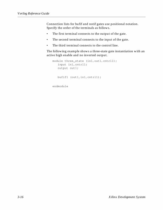
The following example shows a three-state gate instantiation with an active high enable and no inverted output.
module three_state (in1,out1,cntrl1);input in1,cntrl1;output out1;
bufif1 (out1,in1,cntrl1);
endmodule
3-16 Xilinx Development System

Chapter 4
Expressions
In Verilog, expressions consist of a single operand or multiple oper-ands separated by operators. You use expressions where a value is required in Verilog.
This chapter explains how to build and use expressions. The chapter is divided into the following sections.
• “Constant-Valued Expressions”
• “Operators”
• “Operands”
• “Expression Bit Widths”
Constant-Valued ExpressionsA constant-valued expression is an expression whose operands are either constants or parameters. Foundation Express determines the value of these expressions.
In the following example, size-1 is a constant-valued expression. The expression (op == ADD) ? a+b : a-b is not a constant-valued expres-sion because the value depends on the variable op. If the value of op is 1, b is added to a; otherwise, b is subtracted from a.
//all expressions are constant-valued, //except in the assign statement.module add_or_subtract(a,b,op,s); //performs s=a+b if op is ADD // s=a-b if op is not ADD
parameter size=8; parameter ADD=1’b1;
Verilog Reference Guide 4-1

Verilog Reference Guide
input op; input [size-1:0]a,b; output[size-1:0]s;assign s=(op==ADD)? a+b:a-b; //not a constant-
//valued expressionendmodule
The operators and operands used in an expression influence the way that a design is synthesized. Foundation Express evaluates constant-valued expressions and does not synthesize circuitry to compute their value. If an expression contains constants, they are propagated to reduce the amount of circuitry required. However, Foundation Express does synthesize circuitry for an expression that contains variables.
OperatorsOperators identify the operation to be performed on their operands to produce a new value. Most operators are either unary operators, that apply to only one operand, or binary operators, that apply to two operands. Two exceptions are conditional operators, which take three operands, and concatenation operators, which take any number of operands.
Foundation Express supports the Verilog language operators listed in the following table. A description of the operators and their order of precedence is given in the sections following the table.
Table 4-1 Verilog Operators Supported by Foundation Express
Operator Type Operator Description
Arithmetic Operators + - * /%
ArithmeticModules
Relational Operators >>=<<=
Relational
Equality Operators ==! =
Logical equalityLogical inequality
Logical Operators !&&| |
Logical NOTLogical ANDLogical OR
4-2 Xilinx Development System

Expressions
In the following descriptions, the terms variable and variable operand refer to operands or expressions that are not constant-valued expres-sions. This group includes wires and registers, bit-selects and part-selects of wires and registers, function calls, and expressions that contain any of these elements.
Arithmetic OperatorsArithmetic operators perform simple arithmetic on operands. The Verilog arithmetic operators follow.
• Addition (+)
• Subtraction (-)
• Multiplication (*)
• Division (/)
• Modules (%)
You can use the +, -, and * operators with any operand form (constants or variables). You can use the + and - operators as either
Bit-wise Operators ~&|^^~ or ~^
Bit-wise NOTBit-wise ANDBit-wise ORBit-wise XORBit-wise XNOR
Reduction Operators &|~ &~ |^~^ or ^~
Reduction ANDReduction ORReduction NANDReduction NORReduction XORReduction XNOR
Shift Operators <<>>
Shift leftShift right
Conditional Operator ? : Conditions
Concatenation Operator
{ } Concatenation
Table 4-1 Verilog Operators Supported by Foundation Express
Operator Type Operator Description
Verilog Reference Guide 4-3

Verilog Reference Guide
unary or binary operators. Foundation Express requires that / and % operators have constant-valued operands.
The following example shows three forms of the addition operator. The circuitry built for each addition operation is different because of the different operand types. The first addition requires no logic, the second synthesizes an incrementer, and the third synthesizes an adder.
parameter size=8; wire[3:0]a,b,c,d,e;
assign c=size + 2; //constant + constantassign d=a + 1; //variable + constantassign e=a + b; //variable + variable
Relational OperatorsRelational operators compare two quantities and yield a 0 or 1 value. A true comparison evaluates to 1; a false comparison evaluates to 0. All comparisons assume unsigned quantities. The circuitry synthe-sized for relational operators is a bit-wise comparator whose size is based on the sizes of the two operands.
The Verilog relational operators follow.
• Less than (<)
• Less than or equal to (<=)
• Greater than (>)
• Greater than or equal to (>=)
The following example shows a relational operator.
function [7:0] max(a,b); input [7:0] a,b;
if(a>=b) max=a; else max=b;
endfunction
Equality OperatorsEquality operators generate a 0 if compared expressions are not equal and a 1 if the expressions are equal. Equality and inequality compari-sons are performed by bit.
4-4 Xilinx Development System

Expressions
The Verilog equality operators follow.
• Equality (==)
• Inequality (!=)
The following example shows the equality operator used to test for a JMP instruction. The output signal jump is set to 1 if the two high-order bits of instruction are equal to the value of parameter JMP; otherwise, jump is set to 0.
module is_jump_instruction(instruction,jump);parameter JMP=2’h3;
input [7:0] instruction; output jump; assign jump=(instruction[7:6]==JMP);
endmodule
Handling Comparisons to X or ZFoundation Express always ignores comparisons to an X or a Z. If your code contains a comparison to an X or a Z, a warning message is displayed indicating that the comparison is always evaluated to FALSE, which might cause simulation to disagree with synthesis.
The following example shows code from a file called test2.v. Founda-tion Express always assigns Variable B to the value 1, because the comparison to X is ignored.
always beginif (A==1’bx) //this is line 10
B=0;else
B=1;end
When Foundation Express reads this code, it generates the following warning message.
Warning: Comparisons to a “don’t care” are treated as always being false in routine test2 line 10 in file ‘test2.v’. This may cause simulation to disagree with synthesis. (HDL-170)
Verilog Reference Guide 4-5
Verilog Reference Guide
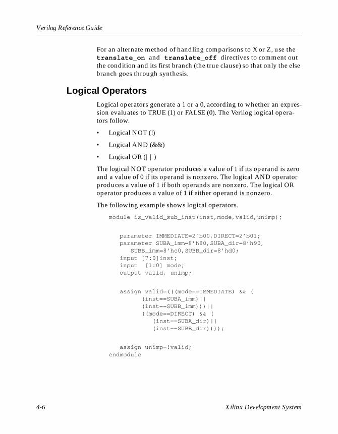
For an alternate method of handling comparisons to X or Z, use the translate_on and translate_off directives to comment out the condition and its first branch (the true clause) so that only the else branch goes through synthesis.
Logical OperatorsLogical operators generate a 1 or a 0, according to whether an expres-sion evaluates to TRUE (1) or FALSE (0). The Verilog logical opera-tors follow.
• Logical NOT (!)
• Logical AND (&&)
• Logical OR (||)
The logical NOT operator produces a value of 1 if its operand is zero and a value of 0 if its operand is nonzero. The logical AND operator produces a value of 1 if both operands are nonzero. The logical OR operator produces a value of 1 if either operand is nonzero.
The following example shows logical operators.
module is_valid_sub_inst(inst,mode,valid,unimp);
parameter IMMEDIATE=2’b00,DIRECT=2’b01;parameter SUBA_imm=8’h80,SUBA_dir=8’h90,
SUBB_imm=8’hc0,SUBB_dir=8’hd0;input [7:0]inst;input [1:0] mode;output valid, unimp;
assign valid=(((mode==IMMEDIATE) && ( (inst==SUBA_imm)|| (inst==SUBB_imm)))||((mode==DIRECT) && (
(inst==SUBA_dir)|| (inst==SUBB_dir))));
assign unimp=!valid; endmodule
4-6 Xilinx Development System

Expressions
Bit-wise OperatorsBit-wise operators act on the operand bit by bit. The Verilog bit-wise operators follow.
• Unary negation (~)
• Binary AND (&)
• Binary OR (|)
• Binary XOR (^)
• Binary XNOR (^~ or ~^)
The following is an example of bit-wise operators.
module full_adder(a,b,cin,s,cout); input a,b,cin; output s,cout;
assign s = a ^ b ^ cin; assign cout = (a & b)|(cin & (a|b));
endmodule
Reduction OperatorsReduction operators take one operand and return a single bit. For example, the reduction AND operator takes the AND value of all the bits of the operand and returns a 1-bit result. The Verilog reduction operators follow.
• Reduction AND (&)
• Reduction OR (|)
• Reduction NAND (~&)
• Reduction NOR (~|)
• Reduction XOR (^)
• Reduction XNOR (^~ or ~^)
The following example shows reduction operators.
module check_input (in, parity, all_ones); input [7:0] in; output parity, all_ones;
Verilog Reference Guide 4-7

Verilog Reference Guide
assign parity = ^ in; assign all_ones = & in;
endmodule
Shift OperatorsA shift operator takes two operands and shifts the value of the first operand right or left by the number of bits given by the second operand.
The Verilog shift operators follow.
• Shift left (<<)
• Shift right (>>)
After the shift, vacated bits are filled with zeros. Shifting by a constant, results in minor circuitry modification (because only rewiring is required). Shifting by a variable causes a general shifter to be synthesized. The following example shows how a shift right oper-ator is used to perform a division by 4.
module divide_by_4 (dividend,quotient); input [7:0] dividend; output [7:0] quotient;
assign quotient = dividend >> 2; //shift right 2 //bits
endmodule
Conditional OperatorThe conditional operator (? :) evaluates an expression and returns a value that is based on the truth of the expression. The following example shows how to use the conditional operator. If the expression (op == ADD) evaluates to TRUE, the value a + b is assigned to result; otherwise, the value a - is assigned to result.
module add_or_subtract (a, b, op, result);
parameter ADD = 1’b0; input [7:0] a, b; input op; output [7:0] result;
4-8 Xilinx Development System
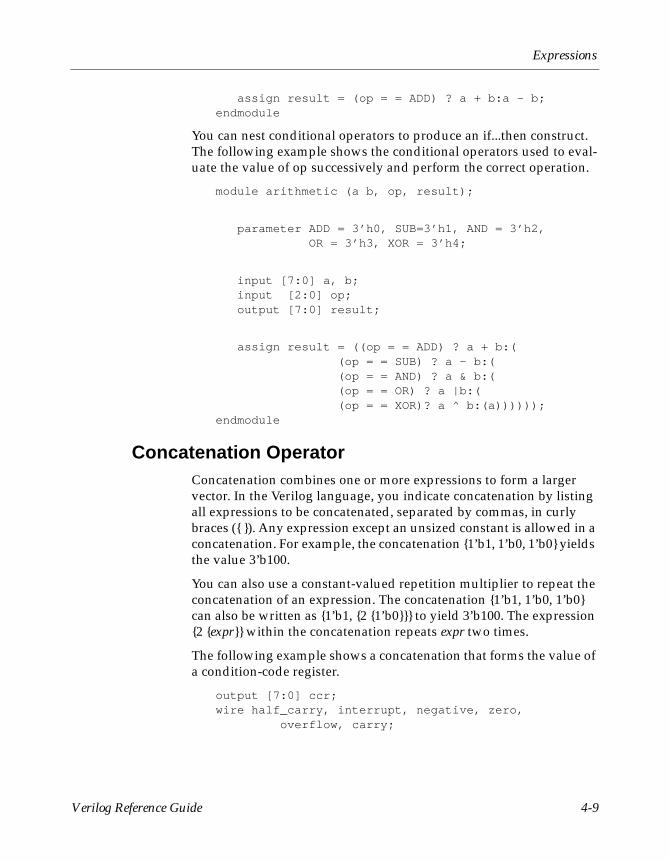
Expressions
assign result = (op = = ADD) ? a + b:a - b;endmodule
You can nest conditional operators to produce an if...then construct. The following example shows the conditional operators used to eval-uate the value of op successively and perform the correct operation.
module arithmetic (a b, op, result);
parameter ADD = 3’h0, SUB=3’h1, AND = 3’h2, OR = 3’h3, XOR = 3’h4;
input [7:0] a, b; input [2:0] op; output [7:0] result;
assign result = ((op = = ADD) ? a + b:( (op = = SUB) ? a - b:( (op = = AND) ? a & b:( (op = = OR) ? a |b:((op = = XOR)? a ^ b:(a))))));
endmodule
Concatenation OperatorConcatenation combines one or more expressions to form a larger vector. In the Verilog language, you indicate concatenation by listing all expressions to be concatenated, separated by commas, in curly braces ({ }). Any expression except an unsized constant is allowed in a concatenation. For example, the concatenation {1’b1, 1’b0, 1’b0} yields the value 3’b100.
You can also use a constant-valued repetition multiplier to repeat the concatenation of an expression. The concatenation {1’b1, 1’b0, 1’b0} can also be written as {1’b1, {2 {1’b0}}} to yield 3’b100. The expression {2 {expr}} within the concatenation repeats expr two times.
The following example shows a concatenation that forms the value of a condition-code register.
output [7:0] ccr;wire half_carry, interrupt, negative, zero,
overflow, carry;
Verilog Reference Guide 4-9

Verilog Reference Guide
... assign ccr = {2’b00, half_carry, interrupt,
negative, zero, overflow, carry};
The following example shows an equivalent description for the concatenation.
output [7:0] ccr;
... assign ccr[7] = 1’b0; assign ccr[6] = 1’b0; assign ccr[5] = half_carry; assign ccr[4] = interrupt; assign ccr[3] = negative;assign ccr[2] = zero;assign ccr[1] = overflow; assign ccr[0] = carry;
Operator PrecedenceThe following table lists the precedence of all operators, from highest to lowest. All operators at the same level in the table are evaluated from left to right, except the conditional operator (?:), which is evalu-ated from right to left.
Table 4-2 Operator Precedence
Operator Description
[ ] Bit-select or part-select
( ) Parentheses
! ~ Logical and bit-wise negation
& | ~& ~| ^ ~^ ^~ Reduction operators
+ - Unary arithmetic
{ } Concatenation
* / % Arithmetic
+ - Arithmetic
<< >> Shift
> >= < <= Relational
== != Logical equality and inequality
& Bit-wise AND
4-10 Xilinx Development System
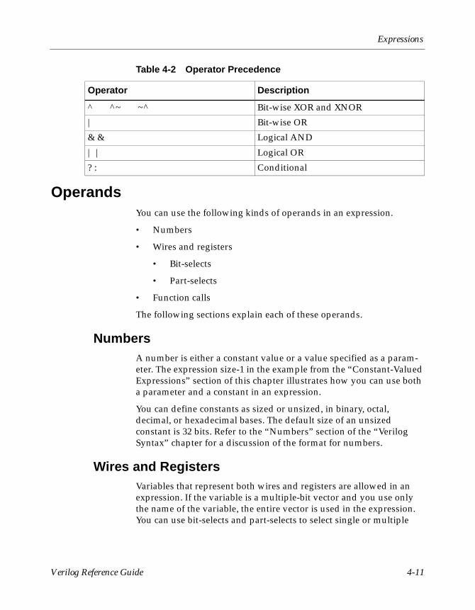
Expressions
OperandsYou can use the following kinds of operands in an expression.
• Numbers
• Wires and registers
• Bit-selects
• Part-selects
• Function calls
The following sections explain each of these operands.
NumbersA number is either a constant value or a value specified as a param-eter. The expression size-1 in the example from the “Constant-Valued Expressions” section of this chapter illustrates how you can use both a parameter and a constant in an expression.
You can define constants as sized or unsized, in binary, octal, decimal, or hexadecimal bases. The default size of an unsized constant is 32 bits. Refer to the “Numbers” section of the “Verilog Syntax” chapter for a discussion of the format for numbers.
Wires and RegistersVariables that represent both wires and registers are allowed in an expression. If the variable is a multiple-bit vector and you use only the name of the variable, the entire vector is used in the expression. You can use bit-selects and part-selects to select single or multiple
^ ^~ ~^ Bit-wise XOR and XNOR
| Bit-wise OR
& & Logical AND
| | Logical OR
? : Conditional
Table 4-2 Operator Precedence
Operator Description
Verilog Reference Guide 4-11

Verilog Reference Guide
bits, respectively, from a vector. These are described in the next two sections.
Wires are described in the “Module Statements and Constructs” section of the “Structural Descriptions” chapter. Registers are described in the “Function Declarations” section of the “Functional Descriptions” chapter.
In the Verilog fragment shown in the following example, a, b, and c are 8-bit vectors of wires. Because only the variable names appear in the expression, the entire vector of each wire is used in evaluating the expression.
wire [7:0] a, b, c; assign c = a & b;
Bit-Selects
A bit-select is the selection of a single bit from a wire, register, or parameter vector. The value of the expression in brackets ( [ ] ) selects the bit you want from the vector. The selected bit must be within the declared range of the vector. The following simple example shows a bit-select with an expression.
wire [7:0] a, b, c; assign c[0] = a [0] & b[0];
Part-Selects
A part-select is the selection of a group of bits from a wire, register, or parameter vector. The part-select expression must be constant-valued in the Verilog language, unlike the bit-select operator. If a variable is declared with ascending indices or descending indices, the part-select (when applied to that variable) must be in the same order.
You can also write the expression in the example of the wire oper-ands (in the “Wires and Registers” section of this chapter) as shown in the example below.
assign c[7:0] = a[7:0] & b[7:0]
Function CallsIn Verilog, you can call one function from inside an expression and use the return value from the called function as an operand. Func-tions in Verilog return a value consisting of one or more bits. The
4-12 Xilinx Development System
Expressions
syntax of a function call is the function name followed by a comma-separated list of function inputs enclosed in parentheses. The following example shows the function call ’legal’ used in an expres-sion.
assign error = ! legal (in1,in2);
Functions are described in the “Function Declarations” section of the “Functional Descriptions” chapter.
Concatenation of OperandsConcatenation is the process of combining several single-bit or multiple-bit operands into one large bit vector. The use of the concat-enation operator, a pair of braces ({ }), is described in the “Concatena-tion Operator” section of this chapter.
The following example shows two 4-bit vectors (nibble1 and nibble2) that are joined to form an 8-bit vector that is assigned to an 8-bit wire vector (byte).
wire [7:0] byte;wire [3:0] nibble1, nibble2;assign byte = {nibble1, nibble2};
Expression Bit WidthsThe bit width of an expression depends on the widths of the oper-ands and the types of operators in the expression.
The “Expression Bit-Widths” table shows the bit-width for each operand and operator. In the table, i, j, and k are expressions; L(i) is the bit-width of expression i.
To preserve significant bits within an expression, Verilog fills in zeros for smaller-width operands. The rules for this zero-extension depend on the operand type. These rules are also listed in the “Expression Bit-Widths” table.
Verilog classifies expressions (and operands) as either self-deter-mined or context-determined. A self-determined expression is one in which the width of the operands is determined solely by the expres-sion itself. These operand widths are never extended.
Verilog Reference Guide 4-13
Verilog Reference Guide
Table 4-3 Expression Bit-Widths
Expression Bit Length Comments
unsized constant 32-bit self-determined
sized constant as specified self-determined
i + j max(L(i),L(j)) context-determined
i - j max(L(i),L(j)) context-determined
i * j max(L(i),L(j)) context-determined
i / j max(L(i),L(j)) context-determined
i % j max(L(i),L(j)) context-determined
i & j max(L(i),L(j)) context-determined
i | j max(L(i),L(j)) context-determined
i ^ j max(L(i),L(j)) context-determined
i ^~ j max(L(i),L(j)) context-determined
~i L(i) context-determined
i == j 1-bit self-determined
i !== j 1-bit self-determined
i && j 1-bit self-determined
i || j 1-bit self-determined
i > j 1-bit self-determined
i >= j 1-bit self-determined
i < j 1-bit self-determined
i <= j 1-bit self-determined
&i 1-bit self-determined
|i 1-bit self-determined
^i 1-bit self-determined
~&i 1-bit self-determined
~|i 1-bit self-determined
~^i 1-bit self-determined
i >> j L(i) j is self-determined
{i{j}} i*L(j) j is self-determined
i << j L(i) j is self-determined
4-14 Xilinx Development System
Expressions
The following example shows a self-determined expression that is a concatenation of variables with known widths.
output [7:0] result;wire [3:0] temp;
assign temp = 4’b1111;assign result = {temp,temp};
The concatenation has two operands. Each operand has a width of four bits and a value of 4’b1111. The resulting width of the concatena-tion is 8 bits, which is the sum of the width of the operands. The value of the concatenation is 8’b11111111.
A context-determined expression is one in which the width of the expression depends on all operand widths in the expression. For example, Verilog defines the resulting width of an addition as the greater of the widths of its two operands. The addition of two 8-bit quantities produces an 8-bit value; however, if the result of the addi-tion is assigned to a 9-bit quantity, the addition produces a 9-bit result. Because the addition operands are context-determined, they are zero-extended to the width of the largest quantity in the entire expression.
The following example shows context-determined expressions.
if (((1’b1 << 15) >> 15) = = 1’b0)//This expression is ALWAYS true.
if ((((1’b1 << 15) >> 15)| 20’b0) = = 1’b0)//This expression is NEVER true.
The expression ((1’b1 << 15) >> 15) produces a 1-bit 0 value (1’b0). The 1 is shifted off of the left end of the vector, producing a value of 0. The right shift has no additional effect. For a shift operator, the first operand (1’b1) is context-dependent; the second operand (15) is self-determined.
i ? j : k Max(L(j),L(k)) j is self-determined
{i,...,j} L(i)+...+L(j) self-determined
{i {j,...,k}} /*(L(j)+...+L(k)) self-determined
Table 4-3 Expression Bit-Widths
Expression Bit Length Comments
Verilog Reference Guide 4-15
Verilog Reference Guide
The expression (((1’b1 << 15) >> 15) | 20’b0) produces a 20-bit 1 value (20’b1). 20’b1 has a 1 in the least significant bit position and 0s in the other 19 bit positions. Because the largest operand within the expres-sion has a width of 20, the first operand of the shift is zero-extended to a 20-bit value. The left shift of 15 does not drop the 1 value off the left end; the right shift brings the 1 value back to the right end, resulting in a 20-bit 1 value (20’b1).
4-16 Xilinx Development System
Chapter 5
Functional Descriptions
A Verilog functional (or Register Transfer Level) description describes a circuit in terms of its registers and the combinatorial logic between the registers.
The following sections of this chapter describe how to construct and use functional descriptions.
• “Sequential Constructs”
• “Function Declarations”
• “Function Statements”
• “task Statements”
• “always Blocks”
Sequential Constructs Although many Verilog constructs appear sequential in nature, they describe combinatorial circuitry. A simple description that appears to be sequential is shown in the following example.
x=b; if (y)
x=x + a;
Foundation Express determines the combinatorial equivalent of this description. In fact, Foundation Express treats the statements in the above example in the same way that it treats the statements in the following example.
if (y) x = b + a;
else x = b;
Verilog Reference Guide 5-1

Verilog Reference Guide
To describe combinatorial logic, you write a sequence of statements and operators to generate the output values you want. For example, suppose the addition operator (+) is not supported, and you want to create a combinatorial, ripple-carry adder. The easiest way to describe this circuit is as a cascade of full adders, as in the following example. The example has eight full adders, with each adder following the one before. From this description, Foundation Express generates a fully combinatorial adder.
function [7:0] adder;input [7:0] a, b;
reg c;integer i;begin
c = 0; for (i = 0;i <= 7; i = i + 1) begin
adder[i] = a[i] ^ b[i ^ c;c = a[i] & b[i] | a[i] & c | b[i] & c;
endend
endfunction
Function DeclarationsUsing a function declaration is one of three methods for describing combinatorial logic. The other two methods are the always block, described in the “always Blocks” section of this chapter and the continuous assignment, described in the “Continuous Assignment” section of the “Structural Descriptions” chapter. You must declare and use Verilog functions within a module. You can call functions from the structural part of a Verilog description by using them in a continuous assignment statement or as a terminal in a module instan-tiation. You can also call functions from other functions or from always blocks.
Foundation Express supports the following Verilog function declara-tions.
• Input declarations
• Output from a function
• Register declarations
• Memory declarations
5-2 Xilinx Development System
Functional Descriptions
• Parameter declarations
• Integer declarations
Functions begin with the keyword function and end with the keyword endfunction. The width of the function’s return value (if any) and the name of the function follow the function keyword, as shown in the syntax below.
function [range] name_of_function;[func_declaration]*statement_or_null
endfunction
Defining the bit range of the return value is optional. Specify the range inside square brackets ( [ ] ). If you do not define the range, a function returns a 1-bit quantity by default. You set the function’s output by assigning it to the function name. A function can contain one or more statements. If you use multiple statements, enclose the statements between a begin...end pair.
The following example shows a simple function declaration.
function [7:0] scramble; input [7:0] a; input [2:0] control; integer i;
begin for (i = 0;i <= 7;i = i + 1)
scramble[i] = a[i ^ control]; end
endfunction
Function statements that Foundation Express supports are discussed under the “Function Statements” section of this chapter.
Input Declarations Verilog input declarations specify the input signals for a function. You must declare the inputs to a Verilog function immediately after you declare the function name. The syntax of input declarations for a function is the same as the syntax of input declarations for a module.
input [range] list_of_variables;
The optional range specification declares an input as a vector of signals. Specify range inside square brackets ( [ ] ).
Verilog Reference Guide 5-3

Verilog Reference Guide
Note: The order in which you declare the inputs must match the order of the inputs in the function call.
Function Output The output from a function is assigned to the function name. A Verilog function has only one output, which can be a vector. For multiple outputs from a function, use the concatenation operation to bundle several values into one return value. This single return value can then be unbundled by the caller. The following example shows how unbundling is done.
function [9:0] signed_addinput [7:0] a, b;
reg [7:0] sum; reg carry, overflow;
begin ... signed_add = carry,overflow,sum};
end endfunction ... assign {C, V, result_bus} = signed_add (busA, busB);
The signed_add function bundles the values of carry, overflow, and sum into one value. This new value is returned in the assign state-ment following the function. The original values are then unbundled by the function that called the signed_add function.
Register Declarations A register represents a variable in Verilog. The syntax for a register declaration follows.
reg [range] list_of_register_variables;
A reg can be a single-bit quantity or a vector of bits. The range param-eter specifies the most significant bit (msb) and least significant bit (lsb) of the vector enclosed in square brackets ( [ ] ). Both bits must be nonnegative constants, parameters, or constant-valued expressions.
The following example shows some reg declarations.
5-4 Xilinx Development System
Functional Descriptions
reg x; //single bit reg a,b,c; //3 single-bit quantities reg [7:0] q; //an 8-bit vector
In Verilog language, you assign a value to a reg variable only within a function or an always block.
In the Verilog simulator, reg variables can hold state information. A reg variable can hold its value across separate calls to a function. In some cases, Foundation Express emulates this behavior by inserting flow-through latches. In other cases, it emulates this behavior without a latch. The concept of holding state is elaborated in the “Inferring Latches” section of the “Register and Three-State Infer-ence” chapter.
Memory DeclarationsThe memory declaration models a bank of registers or memory. In Verilog, the memory declaration is actually a two-dimensional array of reg variables.
The following example shows memory declarations.
reg [7:0] byte_reg;reg [7:0] mem_block [255:0];
In the above example, byte_reg is an 8-bit register and mem_block is an array of 256 registers; each is 8 bits wide. You can index the array of registers to access individual registers, but you cannot access indi-vidual bits of a register directly. Instead, you must copy the appro-priate register into a temporary one-dimensional register. For example, to access the fourth bit of the eighth register in mem_block, enter the following syntax.
byte_reg mem_block [7];individual_bit = byte_reg [3];
Parameter Declarations Parameter variables are local or global variables that hold values. The syntax for a parameter declaration follows.
parameter [range] identifier = expression, identifier = expression;
The range specification is optional.
Verilog Reference Guide 5-5
Verilog Reference Guide
You can declare parameter variables as local to a function. However, you cannot use a local variable outside of that function. Parameter declarations in a function are identical to parameter declarations in a module. The function in the following example contains a parameter declaration.
function gte;parameter width = 8;input [width - 1 : 0] a, b;gte = ( a >= b);
endfunction
Integer DeclarationsInteger variables are local or global variables that hold numeric values. The syntax for an integer declaration follows.
integer identifier_list;
You can declare integer variables locally at the function level or globally at the module level. The default size for integer variables is 32 bits. Foundation Express determines bit-widths, except in the case of a don’t care condition resulting during a compile.
The following example illustrates integer declarations.
integer a; //single 32-bit integer integer b,c; //two integers
Function StatementsFoundation Express supports the following function statements.
• Procedural assignments
• Register transfer level (RTL) assignments
• begin...end block statements
• if...else statements
• case, casex, and casez statements
• for loops
• while loops
• forever loops
• disable statements
5-6 Xilinx Development System

Functional Descriptions
Procedural Assignments Procedural assignments are assignment statements used inside a function. They are similar to the continuous assignment statements described in the “Continuous Assignment” section of the “Structural Descriptions” chapter except that the left side of a procedural assign-ment can contain only reg variables and integers. Assignment state-ments set the value of the left side to the current value of the right side. The right side of the assignment can contain any arbitrary expression of the data types described in the “Structural Data Types” section of the “Structural Descriptions” chapter including simple constants and variables.
The left side of the procedural assignment statement can contain only the following data types.
• reg variables
• Bit-selects of reg variables
• Part-selects of reg variables (must be constant-valued)
• Integers
• Concatenations of the previous data types
Foundation Express assigns the low bit on the right side to the low bit on the left side.
• If the number of bits on the right side is greater than the number on the left side, the high-order bits on the right side are discarded.
• If the number of bits on the left side is greater than the number on the right side, the right side bits are zero-extended.
Foundation Express allows multiple procedural assignments. The following example shows procedural assignments.
sum = a + b; control[5] = (instruction == 8’h2e); {carry_in, a[7:0]} = 9’h 120;
RTL AssignmentsFoundation Express handles variables driven by an RTL (nonblocking) assignment differently than those driven by a proce-dural (blocking) assignment.
Verilog Reference Guide 5-7

Verilog Reference Guide
In procedural assignments, a value passed along from variable A to variable B to variable C results in all three variables having the same value in every clock cycle. In the netlist, procedural assignments are indicated when the input net of one flip-flop is connected to the input net of another flip-flop. Both flip-flops input the same value in the same clock cycle.
In RTL assignments, however, values are passed on in the next clock cycle. Assignment from variable A to variable B occurs after one clock cycle, if variable A has been a previous target of an RTL assignment. Assignment from variable B to variable C always takes place after one clock cycle, because B is the target when RTL assigns variable A’s value to B. In the netlist, an RTL assignment shows flip-flop B receiving its input from the output net of flip-flop A. It takes one clock cycle for the value held by flip-flop Ato propagate to flip-flop B.
A variable can follow only one assignment method and, therefore, cannot be the target of RTL as well as procedural assignments.
The following example is a description of a serial register imple-mented with RTL assignments. The resulting schematic follows the example.
module rtl (clk,data, regc, regd);input data, clk;output regc, regd;
reg regc, regd;
always @ (posedge clk)begin
regc <= data;regd <= regc;
endendmodule
5-8 Xilinx Development System

Functional Descriptions
Figure 5-1 Schematic of RTL Assignments
If you use a procedural assignment, as in the figure above, Founda-tion Express does not synthesize a serial register. Therefore, the recently assigned value of rega, which is data, is assigned to regb, as the schematic in the following figure indicates.
The following example shows a blocking assignment.
module rtl (clk,data, rega, regb);input data, clk;output rega, regb;
reg rega, regb;
always @(posedge clk)begin
rega = data;regb = rega;
endendmodule
X8739
data
clk
regd
regc
Verilog Reference Guide 5-9
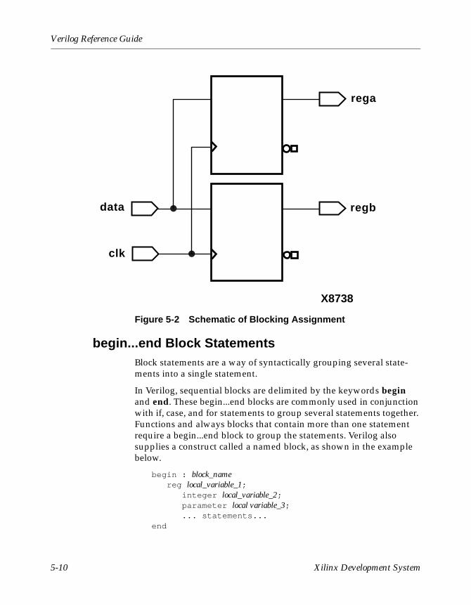
Verilog Reference Guide
Figure 5-2 Schematic of Blocking Assignment
begin...end Block Statements Block statements are a way of syntactically grouping several state-ments into a single statement.
In Verilog, sequential blocks are delimited by the keywords begin and end. These begin...end blocks are commonly used in conjunction with if, case, and for statements to group several statements together. Functions and always blocks that contain more than one statement require a begin...end block to group the statements. Verilog also supplies a construct called a named block, as shown in the example below.
begin : block_name reg local_variable_1;
integer local_variable_2; parameter local variable_3;... statements...
end
X8738
data regb
clk
rega
5-10 Xilinx Development System

Functional Descriptions
In Verilog, no semicolon (;) follows the begin or end keywords. You identify named blocks by following the begin keyword with a colon (:) and a block_name, as shown. You can use Verilog syntax to declare variables locally in a named block. You can include reg, integer, and parameter declarations within a named block but not in an unnamed block. Named blocks allow you to use the disable state-ment.
if...else Statements The if...else statements execute a block of statements according to the value of one or more expressions.
The syntax of if...else statements follows.
if (expr)begin... statements...end
else begin... statements...end
The if statement consists of the keyword if, followed by an expres-sion enclosed in parentheses. The if statement is followed by a state-ment or block of statements enclosed with the begin and end keywords. If the value of the expression is nonzero, the expression is true, and the statement block that follows is executed. If the value of the expression is zero, the expression is false, and the statement block that follows is not executed.
An optional else statement can follow an if statement. If the expres-sion following the if keyword is false, the statement or block of state-ments following the else keyword is executed.
The if...else statements can cause registers to be synthesized. Regis-ters are synthesized when you do not assign a value to the same reg variable in all branches of a conditional construct. Information on registers is detailed in the “Register Inference” section of the “Register and Three-State Inference” chapter.
Foundation Express synthesizes multiplexer logic (or similar select logic) from a single if statement. The conditional expression in an if statement is synthesized as a control signal to a multiplexer, which determines the appropriate path through the multiplexer. For
Verilog Reference Guide 5-11

Verilog Reference Guide
example, the statements in the following example create multiplexer logic controlled by c and place either a or b in the variable x.
if (c)x = a;
elsex = b;
The following example illustrates how if and else can be used to create an arbitrarily long if...else if...else structure.
if (instruction == ADD)begin
carry_in = 0; complement_arg = 0;
end else if (instruction == SUB)
begin carry_in = 1; complement_arg = 1;
end else
illegal_instruction = 1;
The following example shows nested if and else statements.
if (select [1])begin
if (select[0]) out = in[3]; else out = in[2];
end else
begin if (select[0]) out = in[1];else out = in[0];
end
Conditional AssignmentsFoundation Express can synthesize a latch for a conditionally assigned variable. If a path exists that does not explicitly assign a value to a variable, the variable is conditionally assigned. See the “Understanding the Limitations of D Flip-Flop Inference” section of the “Register and Three-State Inference” chapter for more informa-tion.
5-12 Xilinx Development System

Functional Descriptions
In the following example, the variable value is conditionally driven. If c is not true, value is not assigned and retains its previous value.
always beginif (c) beginvalue = x;endy = value; //causes a latch to be synthesized
//for valueend
case Statements The case statement is similar in function to the if...else conditional statement. The case statement allows a multipath branch in logic that is based on the value of an expression. One way to describe a multi-cycle circuit is with a case statement (see the case statement example after the case statement syntax). Another way is with multiple @ (clock edge) statements, which are discussed later in the loop section.
The syntax for a case statement is shown below.
case (expr)case_item1 : begin
...statements...
endcase_item2 : begin
...statements...
enddefault : begin
...statements...end
endcase
The case statement consists of the keyword case, followed by an expression in parentheses, followed by one or more case items (and associated statements to be executed), followed by the keyword endcase. A case item consists of an expression (usually a simple
Verilog Reference Guide 5-13

Verilog Reference Guide
constant) or a list of expressions separated by commas, followed by a colon (:).
The expression following the case keyword is compared with each case item expression, one by one. When the expressions are equal, the condition evaluates to TRUE. Multiple expressions separated by commas can be used in each case item. When multiple expressions are used, the condition is said to be TRUE if any of the expressions in the case item match the expression following the case keyword.
The first case item that evaluates to TRUE determines the path. All subsequent case items are ignored, even if they are true. If no case item is true, no action is taken. You can define a default case item with the expression default, which is used when no other case item is true.
The following example shows a case statement.
case (state) IDLE: begin
if (start) next_state = STEP1;
else next_state = IDLE;
end STEP1: begin
//do first state processing herenext_state = STEP2;
end STEP2: begin
//do second state processing herenext_state = IDLE;
end endcase
Full Case and Parallel CaseFoundation Express automatically determines whether a case state-ment is full or parallel. A case statement is referred to as full case if all possible branches are specified. If you do not specify all possible branches, but you know that one or more branches can never occur, you can declare a case statement as full case with the //synopsys full_case directive. Otherwise, Foundation Express synthesizes a latch. See the “parallel_case Directive” section of the “Foundation
5-14 Xilinx Development System
Functional Descriptions
Express Directives” chapter and “full_case Directive” section of the “Foundation Express Directives” chapter for more information.
Foundation Express synthesizes optimal logic for the control signals of a case statement. If Foundation Express cannot statically determine that branches are parallel, it synthesizes hardware that includes a priority encoder. If Foundation Express can determine that no cases overlap (parallel case), it synthesizes a multiplexer, because a priority encoder is not necessary. You can also declare a case statement as parallel case with the //synopsys parallel_case directive. Refer to the “parallel_case Directive” section of the “Foundation Express Direc-tives” chapter.
The following example is a case statement that is both full and parallel and does not result in either a latch or a priority encoder.
input [1:0] a;always @(a or w or x or y or z) begin
case (a)2’b11:
b = w ;2’b10:
b = x ;2’b01:
b = y ;2’b00:
b = z ;endcase
end
The following example shows a case statement that is parallel but not full that is missing branches for the cases 2’b01 and 2’b10. This example infers a latch for b.
input [1:0] a;always @(a or w or z) begin
case (a)2’b11:
b = w ;2’b00:
b = z ;endcase
end
The case statement in the following example is not parallel or full, because the input values of w and x cannot be determined. However, if you know that only one of the inputs equals 2’b11 at a given time,
Verilog Reference Guide 5-15

Verilog Reference Guide
you can use the // synopsys parallel_case directive to avoid synthe-sizing a priority encoder. If you know that either w or x always equals 2’b11 (a situation known as a one-branch tree), you can use the //synopsys full_case directive to avoid synthesizing a latch.
always @( w or x) begincase (2’b11)
w:b = 10 ;
x:b = 01 ;
endcaseend
casex Statements The casex statement allows a multipath branch in logic according to the value of an expression, just like the case statement. The differ-ences between the case statement and the casex statement are the keyword and the processing of the expressions.
The syntax for a casex statement follows.
casex ( expr)case_item1: begin... statements...endcase_item2: begin... statements...enddefault: begin... statements...end
endcase
A case item can have expressions consisting of the following.
• A simple constant
• A list of identifiers or expressions separated by commas, followed by a colon (:)
• Concatenated, bit-selected, or part-selected expressions
• A constant containing z, x, or ?
5-16 Xilinx Development System

Functional Descriptions
When a z, x, or ? appears in a case-item expression, it means that the corresponding bit of the casex expression is not compared. The following example shows a case item that includes an x.
reg [3:0] cond;casex (cond)
4’b100x: out = 1;default: out = 0;
endcase
In the above example, out is set to 1 if cond is equal to 4’b1000 or 4’b1001, because the last bit of cond is defined as x.
The following example shows a complicated section of code that can be simplified with a casex statement that uses the ? value.
if (cond[3]) out = 0;else if (!cond[3] & cond[2] ) out = 1;else if (!cond[3] & !cond[2] & cond[1] ) out = 2;else if (!cond[3] & !cond[2] & !cond[1] & cond[0] ) out = 3;else if (!cond[3] & !cond[2] & !cond[1] & !cond[0] ) out = 4;
The following example shows the simplified version of the same code.
casex (cond) 4’b1???: out = 0; 4’b01??: out = 1;4’b001?: out = 2; 4’b0001: out = 3;4’b0000: out = 4;
endcase
Foundation Express allows ?, z, and x bits in case items, but not in casex expressions. The following example shows an invalid casex expression.
express = 3’bxz?;...
casex (express) //illegal testing of an expression ...
endcase
casez Statements The casez statement allows a multipath branch in logic according to the value of an expression, just like the case statement. The differ-ences between the case statement and the casez statement are the
Verilog Reference Guide 5-17

Verilog Reference Guide
keyword and the way the expressions are processed. The casez state-ment acts exactly the same as casex, except that x is not allowed in case item; only z and ? are accepted as special characters.
The syntax for a casez statement follows.
casez ( expr )case_item1: begin... statements ...endcase_item2: begin... statements ...enddefault: begin... statements ...end
endcase
A case item can have expressions consisting of the following.
• A simple constant
• A list of identifiers or expressions separated by commas, followed by a colon (:)
• Concatenated, bit-selected, or part-selected expressions
• A constant containing z or ?
When a casez statement is evaluated, the value z in the case item is ignored. An example of a casez statement with z in the case item is shown in the following example.
casez (what_is_it) 2’bz0: begin
//accept anything with least significant bit //zeroit_is = even;
end 2’bz1: begin
//accept anything with least significant bit //oneit_is = odd;
end endcase
Foundation Express allows ? and z bits in case items but not in casez expressions.
5-18 Xilinx Development System
Functional Descriptions
The following example shows an invalid expression in a casez state-ment.
express = 1’bz;...
casez (express) // illegal testing of an expression ...
endcase
for Loops The for loop repeatedly executes a single statement or block of state-ments. The repetitions are performed over a range determined by the range expressions assigned to an index. Two range expressions appear in each for loop: low_range and high_range. In the syntax lines that follow, high_range is greater than or equal to low_range. Foundation Express recognizes both incrementing and decrementing loops. The statement to be duplicated is surrounded by begin and end statements.
Note: Foundation Express allows four syntax forms for a for loop. They include the following.
for (index = low_range;index < high_range;index = index + step)for (index = high_range;index > low_range;index = index - step)for (index = low_range;index <= high_range;index = index + step)for (index = high_range;index >= low_range;index = index - step)
The following example shows a simple for loop.
for (i = 0; i <= 31; i = i + 1) begin s[i] = a[i] ^ b[i] ^ carry; carry = a[i] & b[i] | a[i] & carry |
b[i] & carry; end
For loops can be nested, as shown in the following example.
for (i = 6; i >= 0; i = i - 1) for (j = 0; j <= i; j = j + 1)
if (value[j] > value[j+1]) begin temp = value[j+1]; value[j+1] = value[j]; value[j] = temp;
end
You can use for loops as duplicating statements. The following example shows a for loop.
Verilog Reference Guide 5-19
Verilog Reference Guide
for ( i=0; i < 8; i = i+1 ) example[i] = a[i] & b[7-i];
The following example is the above for loop expanded into its long-hand equivalent.
example[0] = a[0] & b[7]; example[1] = a[1] & b[6]; example[2] = a[2] & b[5]; example[3] = a[3] & b[4]; example[4] = a[4] & b[3]; example[5] = a[5] & b[2]; example[6] = a[6] & b[1]; example[7] = a[7] & b[0];
while LoopsThe while loop executes a statement until the controlling expression evaluates to FALSE. A while loop creates a conditional branch that must be broken by one of the following statements to prevent combi-natorial feedback.
@ (posedge clock) or @ (negedge clock)
Foundation Express supports while loops if you insert one of the following expressions in every path through the loop.
@ (posedge clock) or @ (negedge clock)
The following example shows an unsupported while loop that has no event expression.
alwayswhile (x < y)
x = x + z;
If you add @ (posedge clock) expressions after the while loop in the above example you get the supported version shown in the following example.
alwaysbegin @ (posedge clock)
while (x < y)begin
@ (posedge clock);x = x + z;
endend;
5-20 Xilinx Development System

Functional Descriptions
forever LoopsInfinite loops in Verilog use the keyword forever. You must break up an infinite loop with an @ (posedge clock) or @ (negedge clock) expression to prevent combinatorial feedback, as shown in the example below.
alwaysforeverbegin
@ (posedge clock);x = x + z;
end
You can use forever loops with a disable statement to implement synchronous resets for flip-flops. The disable statement is described in the next section. See the “Register Inference” section of the “Register and Three-State Inference” chapter for more information on synchronous resets.
Using the style illustrated in the example of the supported forever loop above is not recommended, because you cannot test it. The synthesized state machine does not reset to a known state; therefore, it is impossible to create a test program for the state machine. The example of the synchronous reset of state register using disable in a forever loop (in the next section) illustrates how a synchronous reset for the state machine can be synthesized.
disable StatementsFoundation Express supports the disable statement when you use it in named blocks. When a disable statement is executed, it causes the named block to terminate. A comparator description that uses disable is shown in the following example.
begin : compare for (i = 7; i >= 0; i = i - 1) beginif (a[i] != b[i]) begin
greater_than = a[i]; less_than = ~a[i]; equal_to = 0; // comparison is done so stop loopingdisable compare;
end
Verilog Reference Guide 5-21
Verilog Reference Guide
end
//If we get here a == b //If the disable statement is executed,the next three //lines will not be executed
greater_than = 0; less_than = 0; equal_to = 1;
end
Note that the above example describes a combinatorial comparator. Although the description appears sequential, the generated logic runs in a single clock cycle.
You can also use a disable statement to implement a synchronous reset, as shown in the following example.
alwaysforeverbegin: Block
@ (posedge clock)if (Reset)
beginz <= 1’b0disable Block;
endz = a;
end
The disable statement in the example above causes the block reset_label to immediately terminate and return to the beginning of the block.
task StatementsIn Verilog, the task statements are similar to functions except that task statements can have output and inout ports. You can use the task statement to structure your Verilog code so that a portion of code is reusable.
In Verilog, tasks can have timing controls and they can take a nonzero time to return. However, Foundation Express ignores all timing controls, so synthesis might disagree with simulation if the timing controls are critical to the function of the circuit.
5-22 Xilinx Development System

Functional Descriptions
The following example shows how a task statement is used to define an adder function.
module task_example (a, b, c);input [7:0] a, b;output [7:0] c;reg [7:0] c;
task adder;input [7:0] a, b;output [7:0] adder;reg c;integer i;
beginc = 0;for (i = 0; i <= 7; i = i + 1) begin
adder[i] = a[i] ^ b[i] ^ c;c = (a[i] & b[i]) | (a[i] & c) | (b[i] & c);
endend
endtaskalways
adder (a, b, c); // c is a reg
endmodule
Note: Only reg variables can receive output values from a task; wire variables cannot.
always BlocksAn always block can imply latches or flip-flops, or it can specify purely combinatorial logic. An always block can contain logic trig-gered in response to a change in a level or the rising or falling edge of a signal. The syntax of an always block follows.
always @ (event-expression [or event-expression*]) begin... statements ...
end
Verilog Reference Guide 5-23
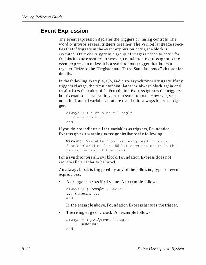
Verilog Reference Guide
Event ExpressionThe event expression declares the triggers or timing controls. The word or groups several triggers together. The Verilog language speci-fies that if triggers in the event expression occur, the block is executed. Only one trigger in a group of triggers needs to occur for the block to be executed. However, Foundation Express ignores the event expression unless it is a synchronous trigger that infers a register. Refer to the “Register and Three-State Inference” chapter for details.
In the following example, a, b, and c are asynchronous triggers. If any triggers change, the simulator simulates the always block again and recalculates the value of f. Foundation Express ignores the triggers in this example because they are not synchronous. However, you must indicate all variables that are read in the always block as trig-gers.
always @ ( a or b or c ) beginf = a & b & c
end
If you do not indicate all the variables as triggers, Foundation Express gives a warning message similar to the following.
Warning: Variable ‘foo’ is being read in block ‘bar’declared on line 88 but does not occur in the timing control of the block.
For a synchronous always block, Foundation Express does not require all variables to be listed.
An always block is triggered by any of the following types of event expressions.
• A change in a specified value. An example follows.
always @ ( identifier ) begin... statements ...end
In the example above, Foundation Express ignores the trigger.
• The rising edge of a clock. An example follows.
always @ ( posedge event ) begin... statements ...
end
5-24 Xilinx Development System

Functional Descriptions
• The falling edge of a clock. An example follows.
always @ ( negedge event ) begin ... statements ...end
• A clock or an asynchronous preload condition. An example follows.
always @ ( posedge CLOCK or negedge reset ) beginif !reset begin... statements ...endelse begin... statements ...end
end
• An asynchronous preload that is based on two events joined by the word or. An example follows.
always @ ( posedge CLOCK or posedge event1 or negedge event2 ) begin
if ( event1 ) begin... statements ...endelse if ( !event2 ) begin... statements ...endelse begin... statements ...end
end
When the event expression does not contain posedge or negedge, combinatorial logic (no registers) is usually generated, although flow-through latches can be generated.
Note: The statements @ (posedge clock) and @ (negedge clock) are not supported in functions or tasks.
Incomplete Event SpecificationAn always block can be misinterpreted if you do not list all signals entering an always block in the event specification.
Foundation Express builds a 3-input AND gate for the description in the following example. However, when this description is simulated,
Verilog Reference Guide 5-25
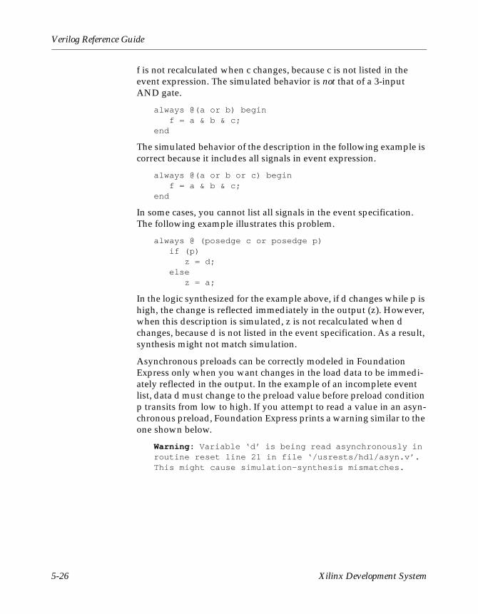
Verilog Reference Guide
f is not recalculated when c changes, because c is not listed in the event expression. The simulated behavior is not that of a 3-input AND gate.
always @(a or b) beginf = a & b & c;
end
The simulated behavior of the description in the following example is correct because it includes all signals in event expression.
always @(a or b or c) beginf = a & b & c;
end
In some cases, you cannot list all signals in the event specification. The following example illustrates this problem.
always @ (posedge c or posedge p)if (p)
z = d;else
z = a;
In the logic synthesized for the example above, if d changes while p is high, the change is reflected immediately in the output (z). However, when this description is simulated, z is not recalculated when d changes, because d is not listed in the event specification. As a result, synthesis might not match simulation.
Asynchronous preloads can be correctly modeled in Foundation Express only when you want changes in the load data to be immedi-ately reflected in the output. In the example of an incomplete event list, data d must change to the preload value before preload condition p transits from low to high. If you attempt to read a value in an asyn-chronous preload, Foundation Express prints a warning similar to the one shown below.
Warning: Variable ‘d’ is being read asynchronously in routine reset line 21 in file ‘/usrests/hdl/asyn.v’. This might cause simulation-synthesis mismatches.
5-26 Xilinx Development System
Chapter 6
Register and Three-State Inference
Foundation Express infers registers (latches and flip-flops) and three-state cells. This chapter explains inference behavior and results in the following sections.
• “Register Inference”
• “Three-State Inference”
Register InferenceBy inferring registers, you can use sequential logic in your designs and keep your designs technology-independent. A register is a simple, one-bit memory device, either a latch or a flip-flop. A latch is a level-sensitive memory device. A flip-flop is an edge-triggered memory device.
Foundation Express’ capability to infer registers supports coding styles other than those described in this chapter. However, for best results, do the following.
• Restrict each always block to a single type of memory-element inferencing: latch, latch with asynchronous set or reset, flip-flop, flip-flop with asynchronous reset, or flip-flop with synchronous reset.
• Use the templates provided in the “Inferring Latches” section and “Inferring Flip-Flops” section of this chapter.
The Inference ReportFoundation Express generates a general inference report when building a design. It provides the asynchronous set or reset, synchro-nous set or reset, and synchronous toggle conditions of each latch or
Verilog Reference Guide 6-1
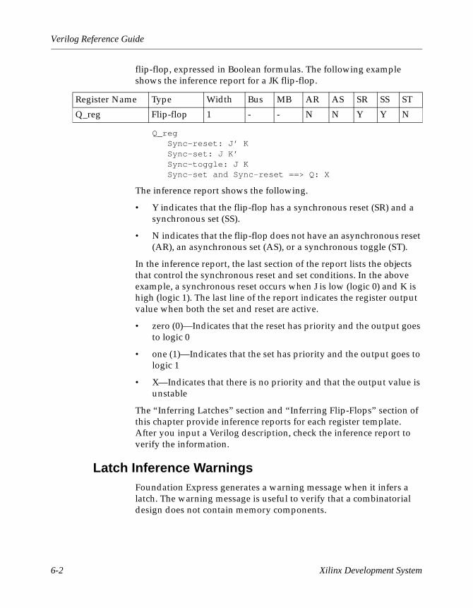
Verilog Reference Guide
flip-flop, expressed in Boolean formulas. The following example shows the inference report for a JK flip-flop.
Q_regSync-reset: J’ KSync-set: J K’Sync-toggle: J KSync-set and Sync-reset ==> Q: X
The inference report shows the following.
• Y indicates that the flip-flop has a synchronous reset (SR) and a synchronous set (SS).
• N indicates that the flip-flop does not have an asynchronous reset (AR), an asynchronous set (AS), or a synchronous toggle (ST).
In the inference report, the last section of the report lists the objects that control the synchronous reset and set conditions. In the above example, a synchronous reset occurs when J is low (logic 0) and K is high (logic 1). The last line of the report indicates the register output value when both the set and reset are active.
• zero (0)—Indicates that the reset has priority and the output goes to logic 0
• one (1)—Indicates that the set has priority and the output goes to logic 1
• X—Indicates that there is no priority and that the output value is unstable
The “Inferring Latches” section and “Inferring Flip-Flops” section of this chapter provide inference reports for each register template. After you input a Verilog description, check the inference report to verify the information.
Latch Inference WarningsFoundation Express generates a warning message when it infers a latch. The warning message is useful to verify that a combinatorial design does not contain memory components.
Register Name Type Width Bus MB AR AS SR SS ST
Q_reg Flip-flop 1 - - N N Y Y N
6-2 Xilinx Development System

Register and Three-State Inference
Controlling Register InferenceUse directives to direct the type of sequential device you want inferred. The default is to implement the type of latch described in the HDL code. These attributes override this behavior.
Foundation Express provides the following directives for controlling register inference.
• async_set_reset
When a signal has this directive set to TRUE, Foundation Express searches for a branch that uses the signal as a condition. Founda-tion Express then checks whether the branch contains an assign-ment to a constant value. If the branch does, the signal becomes an asynchronous reset or set.
Attach the async_set_reset directive to single-bit signals using the following syntax.
// synopsys async_set_reset ” signal_name_list”
• async_set_reset_local
Foundation Express treats listed signals in the specified block as if they have the async_set_reset directive set to TRUE.
Attach the async_set_reset_local directive to a block label using the following syntax.
/* synopsys async_set_reset_local block_label ”signal_name_list” */
• async_set_reset_local_all
Foundation Express treats all signals in the specified blocks as if they have the async_set_reset directive set to TRUE.
Attach the async_set_reset_local_all directive to block labels using the following syntax.
/* synopsys async_set_reset_local_all “ block_label_list” */
• sync_set_reset
When a signal has this directive set to TRUE, Foundation Express checks the signal to determine whether it synchronously sets or resets a register in the design.
Attach the sync_set_reset directive to single-bit signals using the following syntax.
Verilog Reference Guide 6-3
Verilog Reference Guide
//synopsys sync_set_reset ” signal_name_list”
• sync_set_reset_local
Foundation Express treats listed signals in the specified block as if they have the sync_set_reset directive set to TRUE.
Attach the sync_set_reset_local directive to a block label using the following syntax.
/* synopsys sync_set_reset_local block_label ” signal_name_list” */
• sync_set_reset_local_all
Foundation Express treats all signals in the specified blocks as if they have the sync_set_reset directive set to TRUE.
Attach the sync_set_reset_local_all directive to block labels using the following syntax.
/* synopsys sync_set_reset_local_all ” block_label_list” */
• one_cold
A one-cold implementation means that all signals in a group are active low and that only one signal can be active at a given time. The one_cold directive prevents Foundation Express from imple-menting priority encoding logic for the set and reset signals.
Add a check to the Verilog code to ensure that the group of signals has a one-cold implementation. Foundation Express does not produce any logic to check this assertion.
Attach the one_cold directive to set or reset signals on sequential devices using the following syntax.
// synopsys one_cold ” signal_name_list”
• one_hot
A one-hot implementation means that all signals in a group are active-high and that only one signal can be active at a given time. The one_cold directive prevents Foundation Express from imple-menting priority encoding logic for the set and reset signals.
Add a check to the Verilog code to ensure that the group of signals has a one-hot implementation. Foundation Express does not produce any logic to check this assertion.
Attach the one_hot directive to set or reset signals on sequential devices using the following syntax.
6-4 Xilinx Development System
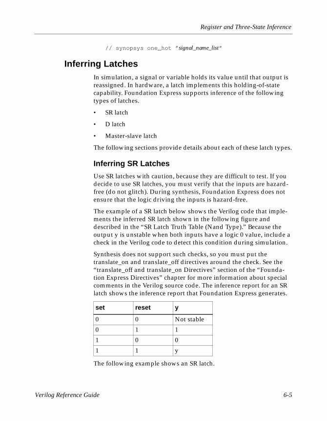
Register and Three-State Inference
// synopsys one_hot ” signal_name_list”
Inferring LatchesIn simulation, a signal or variable holds its value until that output is reassigned. In hardware, a latch implements this holding-of-state capability. Foundation Express supports inference of the following types of latches.
• SR latch
• D latch
• Master-slave latch
The following sections provide details about each of these latch types.
Inferring SR Latches
Use SR latches with caution, because they are difficult to test. If you decide to use SR latches, you must verify that the inputs are hazard-free (do not glitch). During synthesis, Foundation Express does not ensure that the logic driving the inputs is hazard-free.
The example of a SR latch below shows the Verilog code that imple-ments the inferred SR latch shown in the following figure and described in the “SR Latch Truth Table (Nand Type).” Because the output y is unstable when both inputs have a logic 0 value, include a check in the Verilog code to detect this condition during simulation.
Synthesis does not support such checks, so you must put the translate_on and translate_off directives around the check. See the “translate_off and translate_on Directives” section of the “Founda-tion Express Directives” chapter for more information about special comments in the Verilog source code. The inference report for an SR latch shows the inference report that Foundation Express generates.
The following example shows an SR latch.
set reset y
0 0 Not stable
0 1 1
1 0 0
1 1 y
Verilog Reference Guide 6-5

Verilog Reference Guide
module sr_latch (SET, RESET, Q);input SET, RESET;output Q;reg Q;
//synopsys async_set_reset ”SET, RESET”always @(RESET or SET)
if (~RESET)Q = 0;
else if (~SET)Q = 1;
endmodule
The following example shows an inference report for an SR latch.
y_regAsync-reset: RESET’Async-set: SET’Async-set and Async-reset ==> Q: 1
Figure 6-1 SR Latch
Inferring D Latches
When you do not specify the resulting value for a signal under all conditions, as in an incompletely specified if or case statement, Foun-dation Express infers a D latch.
Register Name Type Width Bus MB AR AS SR SS ST
Q_reg Latch 1 - - Y Y - - -
Q
X8590aSET
RESET
6-6 Xilinx Development System

Register and Three-State Inference
For example, the if statement in the following example infers a D latch because there is no else clause. The Verilog code specifies a value for output Q only when input GATE has a logic 1 value. As a result, output Q becomes a latched value.
always @ (DATA or GATE) beginif (GATE) begin
Q = DATA;end
end
The case statement in the following example infers D latches, because the case statement does not provide assignments to decimal for values of I between 10 and 15.
always @(I) begincase(I)
4’h0: decimal= 10’b0000000001;4’h1: decimal= 10’b0000000010;4’h2: decimal= 10’b0000000100;4’h3: decimal= 10’b0000001000;4’h4: decimal= 10’b0000010000;4’h5: decimal= 10’b0000100000;4’h6: decimal= 10’b0001000000;4’h7: decimal= 10’b0010000000;4’h8: decimal= 10’b0100000000;4’h9: decimal= 10’b1000000000;
endcaseend
To avoid latch inference, assign a value to the signal under all condi-tions. To avoid latch inference by the if statement in the above example, modify the block as shown in the following examples. To avoid latch inference by the case statement in the above example, add the following statement before the endcase statement.
default: decimal= 10’b0000000000;
The following example shows how to avoid latch inference.
always @ (DATA, GATE) beginQ = 0;if (GATE)
Q = DATA;end
The following example shows another way to avoid latch inference.
Verilog Reference Guide 6-7
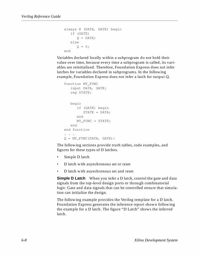
Verilog Reference Guide
always @ (DATA, GATE) beginif (GATE)
Q = DATA;else
Q = 0;end
Variables declared locally within a subprogram do not hold their value over time, because every time a subprogram is called, its vari-ables are reinitialized. Therefore, Foundation Express does not infer latches for variables declared in subprograms. In the following example, Foundation Express does not infer a latch for output Q.
function MY_FUNCinput DATA, GATE;reg STATE;
beginif (GATE) begin
STATE = DATA;endMY_FUNC = STATE;
endend function. . .Q = MY_FUNC(DATA, GATE);
The following sections provide truth tables, code examples, and figures for these types of D latches.
• Simple D latch
• D latch with asynchronous set or reset
• D latch with asynchronous set and reset
Simple D Latch When you infer a D latch, control the gate and data signals from the top-level design ports or through combinatorial logic. Gate and data signals that can be controlled ensure that simula-tion can initialize the design.
The following example provides the Verilog template for a D latch. Foundation Express generates the inference report shown following the example for a D latch. The figure “D Latch” shows the inferred latch.
6-8 Xilinx Development System
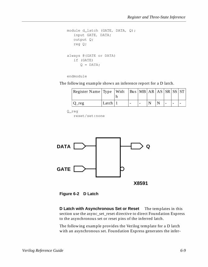
Register and Three-State Inference
module d_latch (GATE, DATA, Q);input GATE, DATA;output Q;reg Q;
always @(GATE or DATA)if (GATE)
Q = DATA;
endmodule
The following example shows an inference report for a D latch.
Q_regreset/set:none
Figure 6-2 D Latch
D Latch with Asynchronous Set or Reset The templates in this section use the async_set_reset directive to direct Foundation Express to the asynchronous set or reset pins of the inferred latch.
The following example provides the Verilog template for a D latch with an asynchronous set. Foundation Express generates the infer-
Register Name Type Width
Bus MB AR AS SR SS ST
Q_reg Latch 1 - - N N - - -
QDATA
GATE
X8591
Verilog Reference Guide 6-9

Verilog Reference Guide
ence report shown following the example for a D latch with asyn-chronous set. The figure “D Latch with Asynchronous Set” shows the inferred latch.
module d_latch_async_set (GATE, DATA, SET, Q);input GATE, DATA, SET;output Q;reg Q;
//synopsys async_set_reset ”SET”always @(GATE or DATA or SET)
if (~SET)Q = 1’b1;
else if (GATE)Q = DATA;
endmodule
The following example shows an inference report for a D latch with asynchronous set.
Q_regAsync-set: SET’
Figure 6-3 Latch with Asynchronous Set
Register Name Type Width
Bus MB AR AS SR SS ST
Q_reg Latch 1 - - N Y - - -
X8592
Q
SET
GATE
DATA
6-10 Xilinx Development System
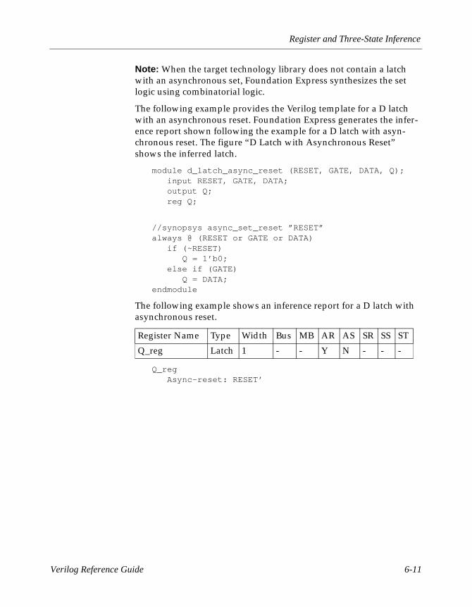
Register and Three-State Inference
Note: When the target technology library does not contain a latch with an asynchronous set, Foundation Express synthesizes the set logic using combinatorial logic.
The following example provides the Verilog template for a D latch with an asynchronous reset. Foundation Express generates the infer-ence report shown following the example for a D latch with asyn-chronous reset. The figure “D Latch with Asynchronous Reset” shows the inferred latch.
module d_latch_async_reset (RESET, GATE, DATA, Q);input RESET, GATE, DATA;output Q;reg Q;
//synopsys async_set_reset ”RESET”always @ (RESET or GATE or DATA)
if (~RESET) Q = 1’b0;
else if (GATE) Q = DATA;
endmodule
The following example shows an inference report for a D latch with asynchronous reset.
Q_regAsync-reset: RESET’
Register Name Type Width Bus MB AR AS SR SS ST
Q_reg Latch 1 - - Y N - - -
Verilog Reference Guide 6-11

Verilog Reference Guide
Figure 6-4 D Latch with Asynchronous Reset
D Latch with Asynchronous Set and Reset The following example provides the Verilog template for a D latch with an active-low asynchronous set and reset. This template uses the async_set_reset_local directive to direct Foundation Express to the asynchronous signals in block infer and uses the one_cold directive to prevent priority encoding of the set and reset signals. For this template, if you do not specify the one_cold directive, the set signal has priority, because it serves as the condition for the if clause. Foun-dation Express generates the inference report shown following the example for a D latch with asynchronous set and reset. The figure “D Latch with Asynchronous Set and Reset” shows the inferred latch.
module d_latch_async (GATE, DATA, RESET, SET, Q);input GATE, DATA, RESET, SET;output Q;reg Q;
// synopsys async_set_reset_local infer ”RESET, SET”// synopsys one_cold ”RESET, SET”always @ (GATE or DATA or RESET or SET)begin : infer
if (!SET) Q = 1’b1;
else if (!RESET)Q = 1’b0;
else if (GATE) Q = DATA;
QDATA
GATE
X8593a
RESET
6-12 Xilinx Development System

Register and Three-State Inference
end
// synopsys translate_offalways @ (RESET or SET)
if (RESET == 1’b0 & SET == 1’b0)$write (”ONE-COLD violation for RESET and SET.”);
// synopsys translate_onendmodule
The following example shows an inference report for a D latch with asynchronous set and reset.
Q_regAsync-reset: RESET’Async-set: SET’Async-set and Async-reset ==> Q: X
Figure 6-5 D Latch with Asynchronous Set and Reset
Understanding the Limitations of D Latch Inference
A variable must always have a value before it is read. As a result, a conditionally assigned variable cannot be read after the if statement in which it is assigned. A conditionally assigned variable is assigned a new value under some, but not all, conditions. The following
Register Name Type Width
Bus MB AR AS SR SS ST
Q_reg Latch 1 - - Y Y - - -
X8594
QSET
GATE
DATA
RESET
Verilog Reference Guide 6-13

Verilog Reference Guide
example shows an invalid use of the conditionally assigned variable VALUE.
begin
if (condition) thenVALUE <= X;
Y <= VALUE; // Invalid read of variable VALUEend
Inferring Master-Slave Latches
You can infer two-phase systems by using D latches. The following example shows a simple two-phase system with clocks MCK and SCK. The figure “Two-Phase Clocks” shows the inferred latches.
module latch_verilog (DATA, MCK, SCK, Q);input DATA, MCK, SCK;output Q;reg Q;
reg TEMP;
always @(DATA or MCK)if (MCK)
TEMP = DATA;
always @(TEMP or SCK)if (SCK)
Q = TEMP;endmodule
6-14 Xilinx Development System

Register and Three-State Inference
Figure 6-6 Two-Phase Clocks
Inferring Flip-FlopsFoundation Express can infer D flip-flops, JK flip-flops, and toggle flip-flops. The following sections provide details about each of these flip-flop types.
Many FPGA devices have a dedicated set/reset hardware resource that should be used. For this reason, you should infer asynchronous set/reset signals for all flip-flops in the design. Foundation Express will then use the global set/reset lines.
Inferring D Flip-Flops
Foundation Express infers a D flip-flop whenever the sensitivity list of an always block includes an edge expression (a test for the rising or falling edge of a signal). Use the following syntax to describe a rising edge.
posedge SIGNAL
Use the following syntax to describe a falling edge.
negedge SIGNAL
When the sensitivity list of an always block contains an edge expres-sion, Foundation Express creates flip-flops for all variables assigned values in the block. The following example shows the most common way of using an always block to infer a flip-flop.
always @(edge)begin
Verilog Reference Guide 6-15

Verilog Reference Guide
.end
Simple D Flip-Flop When you infer a D flip-flop, control the clock and data signals from the top-level design ports or through combina-torial logic. Clock and data signals that can be controlled ensure that simulation can initialize the design. If you cannot control the clock and data signals, infer a D flip-flop with asynchronous reset or set or with a synchronous reset or set.
When you are inferring a simple D flip-flop, the always block can contain only one edge expression.
The following example provides the Verilog template for a positive edge-triggered D flip-flop. Foundation Express generates the infer-ence report shown following the example for a positive edge-trig-gered D flip-flop. The figure “Positive-Edge-Triggered D Flip-flop” shows the inferred flip-flop.
module dff_pos (DATA, CLK, Q);input DATA, CLK;output Q;reg Q;
always @(posedge CLK)Q = DATA;
endmodule
The following example shows an inference report for a positive edge-triggered D flip-flop.
Q_regset/reset/toggle: none
Register Name Type Width Bus MB AR AS SR SS ST
Q_reg Flip-flop 1 - - N N N N N
6-16 Xilinx Development System

Register and Three-State Inference
Figure 6-7 Positive Edge-Triggered D Flip-Flop
The following example provides the Verilog template for a negative edge-triggered D flip-flop. Foundation Express generates the infer-ence report shown following the example for a negative edge-trig-gered D flip-flop. The figure “Negative Edge-Triggered D Flip-Flop” shows the inferred flip-flop.
module dff_neg (DATA, CLK, Q);input DATA, CLK;output Q;reg Q;
always @(negedge CLK)Q = DATA;
endmodule
The following example shows an inference report for a negative edge-triggered D flip-flop.
Q_regset/reset/toggle: none
Register Name Type Width Bus MB AR AS SR SS ST
Q_reg Flip-flop 1 - - N N N N N
QDATA
CLK
X8595
Verilog Reference Guide 6-17
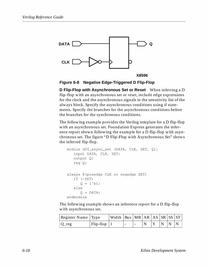
Verilog Reference Guide
Figure 6-8 Negative Edge-Triggered D Flip-Flop
D Flip-Flop with Asynchronous Set or Reset When inferring a D flip-flop with an asynchronous set or reset, include edge expressions for the clock and the asynchronous signals in the sensitivity list of the always block. Specify the asynchronous conditions using if state-ments. Specify the branches for the asynchronous conditions before the branches for the synchronous conditions.
The following example provides the Verilog template for a D flip-flop with an asynchronous set. Foundation Express generates the infer-ence report shown following the example for a D flip-flop with asyn-chronous set. The figure “D Flip-Flop with Asynchronous Set” shows the inferred flip-flop.
module dff_async_set (DATA, CLK, SET, Q);input DATA, CLK, SET;output Q;reg Q;
always @(posedge CLK or negedge SET)if (~SET)
Q = 1’b1;else
Q = DATA;endmodule
The following example shows an inference report for a D flip-flop with asynchronous set.
Register Name Type Width Bus MB AR AS SR SS ST
Q_reg Flip-flop 1 - - N Y N N N
QDATA
CLK
X8596
6-18 Xilinx Development System

Register and Three-State Inference
Q_regAsync-set: SET’
Figure 6-9 D Flip-Flop with Asynchronous Set
The following example provides the Verilog template for a D flip-flop with an asynchronous reset. Foundation Express generates the infer-ence report shown following the example for a D flip-flop with asyn-chronous reset. The figure “D Flip-Flop with Asynchronous Reset” shows the inferred flip-flop.
module dff_async_reset (DATA, CLK, RESET, Q);input DATA, CLK, RESET;output Q;reg Q;
always @(posedge CLK or posedge RESET)if (RESET)
Q = 1’b0;else
Q = DATA;endmodule
The following example shows an inference report for a D flip-flop with asynchronous reset.
Q_regAsync-reset: RESET
Register Name Type Width Bus MB AR AS SR SS ST
Q_reg Flip-flop 1 - - Y N N N N
QDATA
CLK
X8597
SET
Verilog Reference Guide 6-19
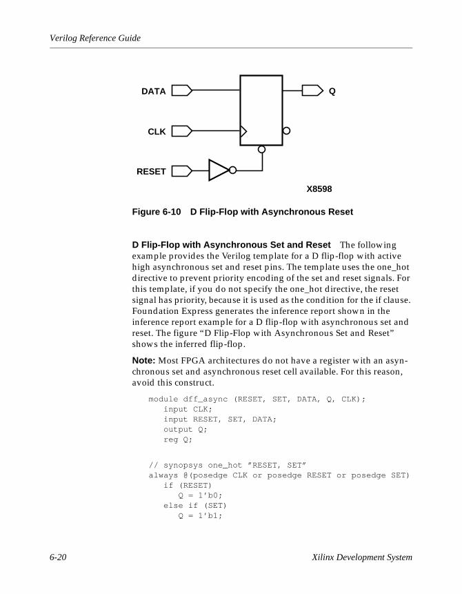
Verilog Reference Guide
Figure 6-10 D Flip-Flop with Asynchronous Reset
D Flip-Flop with Asynchronous Set and Reset The following example provides the Verilog template for a D flip-flop with active high asynchronous set and reset pins. The template uses the one_hot directive to prevent priority encoding of the set and reset signals. For this template, if you do not specify the one_hot directive, the reset signal has priority, because it is used as the condition for the if clause. Foundation Express generates the inference report shown in the inference report example for a D flip-flop with asynchronous set and reset. The figure “D Flip-Flop with Asynchronous Set and Reset” shows the inferred flip-flop.
Note: Most FPGA architectures do not have a register with an asyn-chronous set and asynchronous reset cell available. For this reason, avoid this construct.
module dff_async (RESET, SET, DATA, Q, CLK);input CLK;input RESET, SET, DATA;output Q;reg Q;
// synopsys one_hot ”RESET, SET”always @(posedge CLK or posedge RESET or posedge SET)
if (RESET)Q = 1’b0;
else if (SET)Q = 1’b1;
QDATA
CLK
X8598
RESET
6-20 Xilinx Development System

Register and Three-State Inference
else Q = DATA;
// synopsys translate_offalways @ (RESET or SET)
if (RESET + SET > 1)$write (”ONE-HOT violation for RESET and SET.”);
// synopsys translate_onendmodule
The following example shows an inference report for a D flip-flop with asynchronous set and reset.
Q_regAsync-reset: RESETAsync-set: SETAsync-set and Async-reset ==> Q: X
Figure 6-11 D Flip-flop with Asynchronous Set and Reset
D Flip-Flop with Synchronous Set or Reset The previous exam-ples illustrate how to infer a D flip-flop with asynchronous controls—one way to initialize or control the state of a sequential device. You can also synchronously reset or set the flip-flop (see the examples in this section). The sync_set_reset directive directs Foundation Express to the synchronous controls of the sequential device.
Register Name Type Width Bus MB AR AS SR SS ST
Q_reg Flip-flop 1 - - Y Y N N N
Q
CLK
RESET
DATA
SET
X8599
Verilog Reference Guide 6-21
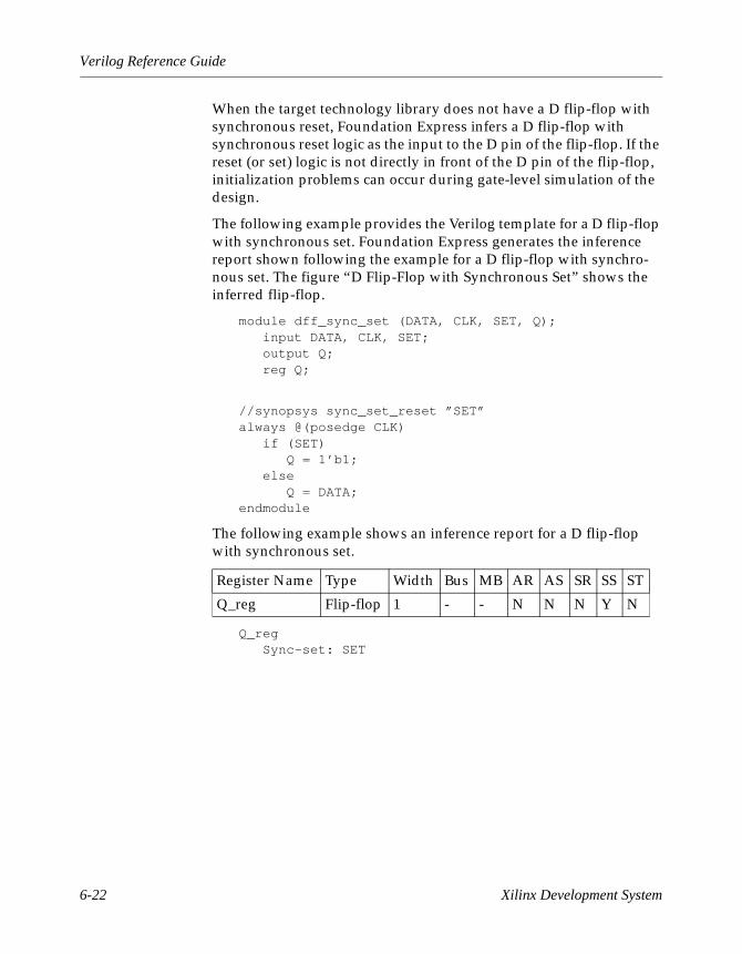
Verilog Reference Guide
When the target technology library does not have a D flip-flop with synchronous reset, Foundation Express infers a D flip-flop with synchronous reset logic as the input to the D pin of the flip-flop. If the reset (or set) logic is not directly in front of the D pin of the flip-flop, initialization problems can occur during gate-level simulation of the design.
The following example provides the Verilog template for a D flip-flop with synchronous set. Foundation Express generates the inference report shown following the example for a D flip-flop with synchro-nous set. The figure “D Flip-Flop with Synchronous Set” shows the inferred flip-flop.
module dff_sync_set (DATA, CLK, SET, Q);input DATA, CLK, SET;output Q;reg Q;
//synopsys sync_set_reset ”SET”always @(posedge CLK)
if (SET)Q = 1’b1;
else Q = DATA;
endmodule
The following example shows an inference report for a D flip-flop with synchronous set.
Q_regSync-set: SET
Register Name Type Width Bus MB AR AS SR SS ST
Q_reg Flip-flop 1 - - N N N Y N
6-22 Xilinx Development System

Register and Three-State Inference
Figure 6-12 D Flip-Flop with Synchronous Set
The following example provides the Verilog template for a D flip-flop with synchronous reset. Foundation Express generates the inference report shown following the example for a D flip-flop with synchro-nous reset. The figure “D Flip-Flop with Synchronous Reset” shows the inferred flip-flop.
module dff_sync_reset (DATA, CLK, RESET, Q);input DATA, CLK, RESET;output Q;reg Q;
//synopsys sync_set_reset ”RESET”always @(posedge CLK)
if (~RESET)Q = 1’b0;
else Q = DATA;
endmodule
The following example shows an inference report for a D flip-flop with synchronous reset.
Q_regSync-reset: RESET’
Register Name Type Width Bus MB AR AS SR SS ST
Q_reg Flip-flop 1 - - N N Y N N
SET
DATA
CLK
Q
X8600
Verilog Reference Guide 6-23
Verilog Reference Guide
Figure 6-13 D Flip-Flop with Synchronous Reset
D Flip-Flop with Synchronous and Asynchronous Load D flip-flops can have asynchronous or synchronous controls. To infer a component with both synchronous and asynchronous controls, you must check the asynchronous conditions before you check the synchronous conditions.
The following example provides the Verilog template for a D flip-flop with synchronous load (called SLOAD) and an asynchronous load (called ALOAD). Foundation Express generates the inference report shown following the example for a D flip-flop with synchronous and asynchronous load. The figure “D Flip-Flop with Synchronous and Asynchronous Load” shows the inferred flip-flop.
module dff_a_s_load (ALOAD, SLOAD, ADATA, SDATA, CLK, Q);input ALOAD, ADATA, SLOAD, SDATA, CLK;output Q;reg Q;
always @ (posedge CLK or posedge ALOAD)if (ALOAD)
Q = ADATA;else if (SLOAD)
Q = SDATA;endmodule
RESET
DATA
CLK
Q
X8601
6-24 Xilinx Development System
Register and Three-State Inference
The following example shows an inference report for a D flip-flop with synchronous and asynchronous load.
Q_regset/reset/toggle: none
Figure 6-14 D Flip-Flop with Synchronous and Asynchronous Load
Multiple Flip-Flops with Asynchronous and Synchronous Controls If a signal is synchronous in one block but asynchronous in another block, use the sync_set_reset_local and async_set_reset_local directives to direct Foundation Express to the correct implementation.
In the following example, block infer_sync uses the reset signal as a synchronous reset, while block infer_async uses the reset signal as an asynchronous reset. Foundation Express generates the inference report shown in the inference reports example for multiple flip-flops with asynchronous and synchronous controls. The figure “Multiple Flip-flops with Asynchronous and Synchronous Controls” shows the resulting design.
module multi_attr (DATA1, DATA2, CLK, RESET, SLOAD, Q1, Q2);input DATA1, DATA2, CLK, RESET, SLOAD;
Register Name Type Width
Bus MB AR AS SR SS ST
Q_reg Flip-flop 1 - - N N N N N
X8602
ALOAD
Q
ADATA
SLOADSDATA
CLK
Verilog Reference Guide 6-25

Verilog Reference Guide
output Q1, Q2;reg Q1, Q2;
//synopsys sync_set_reset_local infer_sync ”RESET”always @(posedge CLK)begin : infer_sync
if (~RESET)Q1 = 1’b0;
else if (SLOAD)Q1 = DATA1; // note: else hold Q
end
//synopsys async_set_reset_local infer_async ”RESET”always @(posedge CLK or negedge RESET)begin: infer_async
if (~RESET)Q2 = 1’b0;
else if (SLOAD)Q2 = DATA2;
endendmodule
The following example shows inference reports for multiple flip-flops with asynchronous and synchronous controls.
Q1_regSync-reset: RESET’
Q2_regAsync-reset: RESET’
Register Name Type Width Bus MB AR AS SR SS ST
Q1_reg Flip-flop 1 - - N N Y N N
Register Name Type Width Bus MB AR AS SR SS ST
Q2_reg Flip-flop 1 - - Y N N N N
6-26 Xilinx Development System
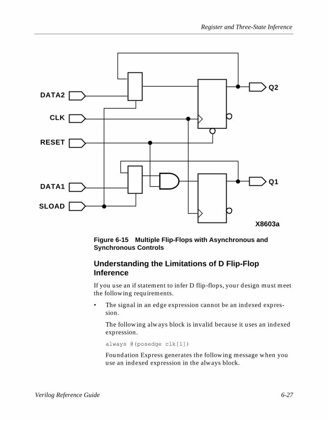
Register and Three-State Inference
Figure 6-15 Multiple Flip-Flops with Asynchronous and Synchronous Controls
Understanding the Limitations of D Flip-Flop Inference
If you use an if statement to infer D flip-flops, your design must meet the following requirements.
• The signal in an edge expression cannot be an indexed expres-sion.
The following always block is invalid because it uses an indexed expression.
always @(posedge clk[1])
Foundation Express generates the following message when you use an indexed expression in the always block.
X8603a
DATA2
DATA1Q1
Q2
SLOAD
CLK
RESET
Verilog Reference Guide 6-27

Verilog Reference Guide
Error: In an event expression with ’posedge’ and ’negedge’ qualifiers, only simple identifiers are allowed %s. (VE-91)
• Set and reset conditions must be single-bit variables.
The following reset condition is invalid because it uses a bused variable.
always @(posedge clk and negedge reset_bus)if (!reset_bus[1]).
end
Foundation Express generates the following message when you use a bused variable in a set or reset condition.
Error: The expression for the reset condition of the ’if’ statement in this ’always’ block can only be a simple identifier or its negation (%s). (VE-92)
• Set and reset conditions cannot use complex expressions.
The following reset condition is invalid because it uses a complex expression.
always @(posedge clk and negedge reset)if (reset == (1-1)).
end
Foundation Express generates the VE-92 message when you use a complex expression in a set or reset condition.
• An if statement must occur at the top level of the always block.
The following example is invalid because the if statement does not occur at the top level.
always @(posedge clk or posedge reset) begin#1;if (reset).
end
Foundation Express generates the following message when the if statement does not occur at the top level.
Error: The statements in this ’always’ block are outside the scope of the synthesis policy (%s). Only an ’if’ statement is allowed at the top level in this
6-28 Xilinx Development System

Register and Three-State Inference
’always’ block. Please refer to the HDL Compiler reference manual for ways to infer flip-flops and latches from ’always’ blocks. (VE-93)
Inferring JK Flip-Flops
When you infer a JK flip-flop, make sure you can control the J, K, and clock signals from the top-level design ports to ensure that simulation can initialize the design.The following sections provide code exam-ples, inference reports, and figures for these types of JK flip-flops:
• JK flip-flop
• JK flip-flop with asynchronous set and reset
JK Flip-Flop In the JK flip-flop, the J and K signals act as active-high synchronous set and reset. Use the sync_set_reset directive to indicate that the J and K signals are the synchronous set and reset for the design. The following table shows the inferred flip-flop..
The following example provides the Verilog code that implements the JK flip-flop described in the ”Truth Table for JK Flip-Flop.”
module JK(J, K, CLK, Q);input J, K;input CLK;output Q;reg Q;
// synopsys sync_set_reset ”J, K”always @ (posedge CLK)
case ({J, K})2’b01 : Q = 0;2’b10 : Q = 1;2’b11 : Q = ~Q;
Table 6-1 Truth Table for JK Flip-Flop
J K CLK Qn+1
0 0 Rising Qn
0 1 Rising 0
1 0 Rising 1
1 1 Rising QnB
X X Falling Qn
Verilog Reference Guide 6-29

Verilog Reference Guide
endcaseendmodule
The following example shows the inference report generated by Foundation Express for a JK flip-flop, and the figure following the report, “JK Flip-Flop,” shows the inferred flip-flop.
Q_regSync-reset: J’ KSync-set: J K’Sync-toggle: J KSync-set and Sync-reset ==> Q: X
Figure 6-16 JK Flip-Flop
JK Flip-Flop With Asynchronous Set and Reset Use the sync_set_reset directive to indicate the JK function. Use the one_hot directive to prevent priority encoding of the J and K signals.
The following example provides the Verilog template for a JK flip-flop with asynchronous set and reset.
module jk_async_sr (RESET, SET, J, K, CLK, Q);input RESET, SET, J, K, CLK;output Q;
Register Name Type Width
Bus MB AR AS SR SS ST
Q_reg Flip-flop 1 - - N N Y Y Y
6-30 Xilinx Development System

Register and Three-State Inference
reg Q;
// synopsys sync_set_reset ”J, K”// synopsys one_hot ”RESET, SET”always @ (posedge CLK or posedge RESET or posedge SET)
if (RESET)Q = 1’b0;
else if (SET)Q = 1’b1;
elsecase ({J, K})
2’b01 : Q = 0;2’b10 : Q = 1;2’b11 : Q = ~Q;
endcase
//synopsys translate_offalways @(RESET or SET)
if (RESET + SET > 1)$write (”ONE-HOT violation for RESET and SET.”);
// synopsys translate_onendmodule
The following table shows the inference report Foundation Express generates for a JK flip-flop with asynchronous set and reset, and the figure following the report, “JK Flip-Flop with Asynchronous Set and Reset,” shows the inferred flip-flop.
Q_reg Async-reset: RESET Async-set: SET Sync-reset: J’ K Sync-set: J K’ Sync-toggle: J K Async-set and Async-reset ==> Q: X Sync-set and Sync-reset ==> Q: X
Register Name Type Width
Bus MB AR AS SR SS ST
Q_reg Flip-flop 1 - - Y Y Y Y Y
Verilog Reference Guide 6-31
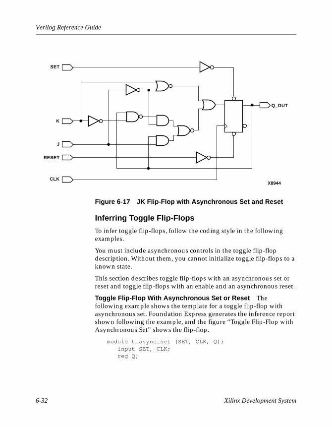
Verilog Reference Guide
Figure 6-17 JK Flip-Flop with Asynchronous Set and Reset
Inferring Toggle Flip-Flops
To infer toggle flip-flops, follow the coding style in the following examples.
You must include asynchronous controls in the toggle flip-flop description. Without them, you cannot initialize toggle flip-flops to a known state.
This section describes toggle flip-flops with an asynchronous set or reset and toggle flip-flops with an enable and an asynchronous reset.
Toggle Flip-Flop With Asynchronous Set or Reset The following example shows the template for a toggle flip-flop with asynchronous set. Foundation Express generates the inference report shown following the example, and the figure “Toggle Flip-Flop with Asynchronous Set” shows the flip-flop.
module t_async_set (SET, CLK, Q);input SET, CLK;reg Q;
X8944
SET
CLK
Q_OUT
RESET
K
J
6-32 Xilinx Development System

Register and Three-State Inference
always @ (posedge CLK or posedge SET)if (SET)
Q = 1;else
Q = ~Q;endmodule
TMP_Q_regAsync-set: SETSync-toggle: true
Figure 6-18 Toggle Flip-Flop with Asynchronous Set
The following example provides the Verilog template for a toggle flip-flop with asynchronous reset. The table following the example shows the inference report, and the figure following the report, “Toggle Flip-Flop with Asynchronous Reset,” shows the inferred flip-flop.
module t_async_reset (RESET, CLK, Q);input RESET, CLK;output Q;reg Q;
Register Name Type Width Bus MB AR AS SR SS ST
TMP_Q_reg Flip-flop 1 - - N Y N N Y
Verilog Reference Guide 6-33
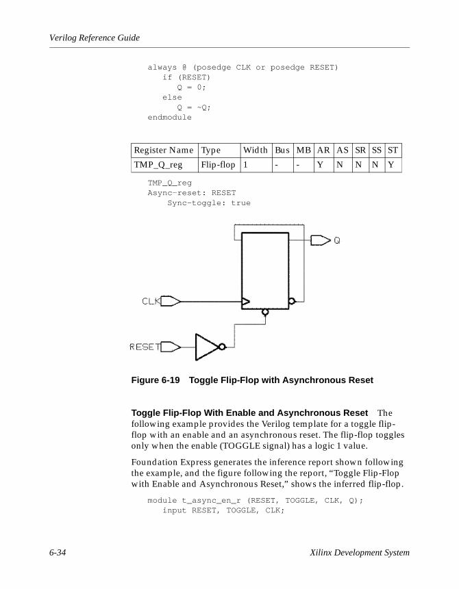
Verilog Reference Guide
always @ (posedge CLK or posedge RESET)if (RESET)
Q = 0;else
Q = ~Q;endmodule
TMP_Q_regAsync-reset: RESET Sync-toggle: true
Figure 6-19 Toggle Flip-Flop with Asynchronous Reset
Toggle Flip-Flop With Enable and Asynchronous Reset The following example provides the Verilog template for a toggle flip-flop with an enable and an asynchronous reset. The flip-flop toggles only when the enable (TOGGLE signal) has a logic 1 value.
Foundation Express generates the inference report shown following the example, and the figure following the report, “Toggle Flip-Flop with Enable and Asynchronous Reset,” shows the inferred flip-flop.
module t_async_en_r (RESET, TOGGLE, CLK, Q);input RESET, TOGGLE, CLK;
Register Name Type Width Bus MB AR AS SR SS ST
TMP_Q_reg Flip-flop 1 - - Y N N N Y
6-34 Xilinx Development System

Register and Three-State Inference
output Q;reg Q;
always @ (posedge CLK or posedge RESET)begin : infer
if (RESET) Q = 0;
else if (TOGGLE)Q = ~Q;
end endmodule
TMP_Q_regAsync-reset: RESETSync-toggle: TOGGLE
Figure 6-20 Toggle Flip-Flop with Enable and Asynchronous Reset
Getting the Best Results
This section provides tips for improving the results you achieve during flip-flop inference. The following topics are covered.
• Minimizing flip-flop count
Register Name Type Width Bus MB AR AS SR SS ST
TMP_Q_reg Flip-flop 1 - - Y N N N Y
Verilog Reference Guide 6-35

Verilog Reference Guide
• Correlating synthesis results with simulation results
Minimizing Flip-Flop Count
An always block that contains a clock edge in the sensitivity list causes Foundation Express to infer a flip-flop for each variable assigned a value in that block. Make sure your HDL description builds only as many flip-flops as the design requires.
The description in the following example builds six flip-flops, one for each variable assigned a value in the block (COUNT(2:0), AND_BITS, OR_BITS, and XOR_BITS).
module count (CLK, RESET, AND_BITS, OR_BITS, XOR_BITS);input CLK, RESET;output AND_BITS, OR_BITS, XOR_BITS;reg AND_BITS, OR_BITS, XOR_BITS;
reg [2:0] COUNT;
always @(posedge CLK) beginif (RESET)
COUNT = 0;else
COUNT = COUNT + 1;
AND_BITS = & COUNT;OR_BITS = | COUNT;XOR_BITS = ^ COUNT;
endendmodule
In the above design, the outputs AND_BITS, OR_BITS, and XOR_BITS depend solely on the value of variable COUNT. If the variable COUNT is registered, these three outputs do not need to be registered.
To compute values synchronously and store them in flip-flops, set up an always block with a signal edge trigger. To let other values change asynchronously, make a separate always block with no signal edge trigger. Put the assignments you want clocked in the always block with the signal edge trigger, and put the other assignments in the other always block. You use this technique to create Mealy machines.
6-36 Xilinx Development System
Register and Three-State Inference
To avoid inferring extra registers, assign the outputs in an always block that does not have a clock edge in its condition expression. The following example shows a description with two always blocks, one with a clock edge condition and one without. Put the registered (synchronous) assignments into the block with the clock edge condi-tion. Put the other (asynchronous) assignments in the other block. This description style lets you choose the variables that are registered and those that are not.
module count (CLK, RESET, AND_BITS, OR_BITS, XOR_BITS);input CLK, RESET;output AND_BITS, OR_BITS, XOR_BITS;reg AND_BITS, OR_BITS, XOR_BITS;
reg [2:0] COUNT;
//synchronous blockalways @(posedge CLK) begin
if (RESET)COUNT = 0;
elseCOUNT = COUNT + 1;
end//asynchronous blockalways @(COUNT) begin
AND_BITS = & COUNT;OR_BITS = | COUNT;XOR_BITS = ^ COUNT;
endendmodule
The technique of separating combinatorial logic from registered or sequential logic is useful to describe state machines. See the following examples in Appendix A.
• “Count Zeros—Combinatorial Version”
• “Count Zeros—Sequential Version”
• “Drink Machine—State Machine Version”
• “Drink Machine—Count Nickels Version”
• “Carry-Lookahead Adder”
Verilog Reference Guide 6-37
Verilog Reference Guide
Correlating with Simulation Results
Using delay specifications with registered values can cause the simu-lation to behave differently from the logic Foundation Express synthesizes. For example, the description in the following example contains delay information that causes Foundation Express to synthe-size a circuit that behaves unexpectedly (the post-synthesis simula-tion results do not match the pre-synthesis simulation results).
module flip_flop (D, CLK, Q);input D, CLK;output Q;.
endmodule
module top (A, C, D, CLK);.reg B;
always @ (A or C or D or CLK)begin
B <= #100 A;flip_flop F1(A, CLK, C);flip_flop F2(B, CLK, D);
endendmodule
In the above example, B changes 100 nanoseconds after A changes. If the clock period is less than 100 nanoseconds, output D is one or more clock cycles behind output C during simulation of the design. However, because Foundation Express ignores the delay informa-tion, A and B change values at the same time and so do C and D. This behavior is not the same as in the post-synthesis simulation.
When using delay information in your designs, make sure that the delays do not affect registered values. In general, you can safely include delay information in your description if it does not change the value that gets clocked into a flip-flop.
Understanding Limitations of Register InferenceFoundation Express cannot infer the following components. You must instantiate these components in your Verilog description.
• Flip-flops and latches with three-state outputs
6-38 Xilinx Development System

Register and Three-State Inference
• Flip-flops with bidirectional pins
• Flip-flips with multiple clock inputs
• Multiport latches
• Register banks
Note: Although you can instantiate flip-flops with bidirectional pins, Foundation Express interprets these cells as black boxes.
Three-State InferenceFoundation Express infers a three-state driver when you assign the value of z to a variable. The z value represents the high-impedance state. Foundation Express infers one three-state driver per block. You can assign high-impedance values to single-bit or bused variables.
Reporting Three-State InferenceFoundation Express generates an inference report that shows infor-mation about inferred devices.
The following example shows a three-state inference report.
The first column of the report indicates the name of the inferred three-state device. The second column of the report indicates the type of three-state device that Foundation Express inferred.
Controlling Three-State InferenceFoundation Express always infers a three-state driver when you assign the value of z to a variable. Foundation Express does not provide any means of controlling the inference.
Inferring Three-State DriversThis section contains Verilog examples that infer the following types of three-state drivers.
• Simple three-state drivers
• Registered three-state drivers
Three-State Device Name Type MB
OUT1_tri Three-State Buffer N
Verilog Reference Guide 6-39

Verilog Reference Guide
Simple Three-State Driver
This section shows a template for a simple three-state driver. In addi-tion, this section supplies examples of how allocating high-imped-ance assignments to different blocks affects three-state inference.
The following example provides the Verilog template for a simple three-state driver. Foundation Express generates the inference report shown in the inference report example for a simple three-state driver. The figure “Three-State Driver” shows the inferred three-state driver.
module three_state (ENABLE, IN1, OUT1);input IN1, ENABLE;output OUT1;reg OUT1;
always @(ENABLE or IN1) beginif (ENABLE)
OUT1 = IN1;else
OUT1 = 1’bz; //assigns high-impedance stateendendmodule
The following example shows an inference report for a simple three-state driver.
Figure 6-21 Three-State Driver
The following example shows how to place all high-impedance assignments in a single block. In this case, the data is gated and Foun-dation Express infers a single three-state driver. An inference report for a single process follows the example. The figure “Inferring One Three-State Driver” shows the schematic the code generates.
Three-State Device Name Type MB
OUT1_tri Three-State Buffer N
X8604
IN1 OUT1
ENABLE
6-40 Xilinx Development System

Register and Three-State Inference
module three_state (A, B, SELA, SELB, T);input A, B, SELA, SELB;output T;reg T;
always @(SELA or SELB or A or B) beginT = 1’bz;if (SELA)
T = A;if (SELB)
T = B;endendmodule
The following example shows a single block inference report.
Figure 6-22 Inferring One Three-State Driver
The following example shows how to place each high-impedance assignment in a separate block. In this case, Foundation Express infers multiple three-state drivers. The inference report for two three-state drivers follows the example. The figure “Inferring Two Three-State Drivers” shows the schematic the code generates.
module three_state (A, B, SELA, SELB, T);input A, B, SELA, SELB;output T;reg T;
Three-State Device Name Type MB
T_tri Three-State Buffer N
X8605
A
B
SELA
SELB
T
Verilog Reference Guide 6-41
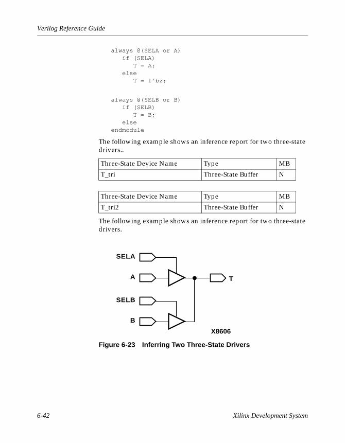
Verilog Reference Guide
always @(SELA or A)if (SELA)
T = A;else
T = 1’bz;
always @(SELB or B)if (SELB)
T = B;else
endmodule
The following example shows an inference report for two three-state drivers..
The following example shows an inference report for two three-state drivers.
Figure 6-23 Inferring Two Three-State Drivers
Three-State Device Name Type MB
T_tri Three-State Buffer N
Three-State Device Name Type MB
T_tri2 Three-State Buffer N
X8606
A T
SELA
B
SELB
6-42 Xilinx Development System

Register and Three-State Inference
Registered Three-State Drivers
When a variable is registered in the same block in which it is three-stated, Foundation Express also registers the enable pin of the three-state gate.
The following example shows this type of code, and the inference report for a three-state driver with registered enable follows the example. The figure “Three-State Driver with Registered Enable” shows the schematic the code generates.
module ff_3state (DATA, CLK, THREE_STATE, OUT1);input DATA, CLK, THREE_STATE;output OUT1;reg OUT1;
always @ (posedge CLK) beginif (THREE_STATE)
OUT1 = 1’bz;else
OUT1 = DATA;endendmodule
The following example shows an inference report for a three-state driver with registered enable.
Three-state Device Name Type MB
OUT1_triOUT1_tr_enable_reg
Three-State BufferFlip-flop (width 1)
NN
Verilog Reference Guide 6-43
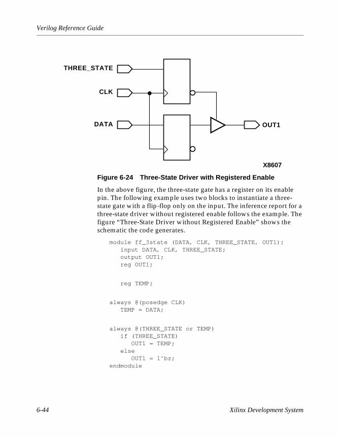
Verilog Reference Guide
Figure 6-24 Three-State Driver with Registered Enable
In the above figure, the three-state gate has a register on its enable pin. The following example uses two blocks to instantiate a three-state gate with a flip-flop only on the input. The inference report for a three-state driver without registered enable follows the example. The figure “Three-State Driver without Registered Enable” shows the schematic the code generates.
module ff_3state (DATA, CLK, THREE_STATE, OUT1);input DATA, CLK, THREE_STATE;output OUT1;reg OUT1;
reg TEMP;
always @(posedge CLK)TEMP = DATA;
always @(THREE_STATE or TEMP)if (THREE_STATE)
OUT1 = TEMP;else
OUT1 = 1’bz;endmodule
THREE_STATE
CLK
X8607
DATA OUT1
6-44 Xilinx Development System
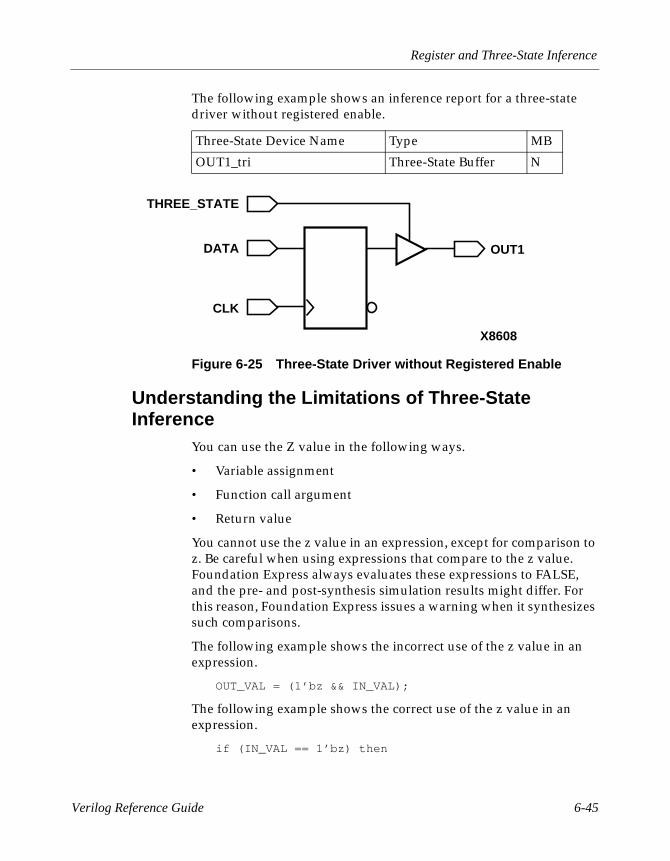
Register and Three-State Inference
The following example shows an inference report for a three-state driver without registered enable.
Figure 6-25 Three-State Driver without Registered Enable
Understanding the Limitations of Three-State Inference
You can use the Z value in the following ways.
• Variable assignment
• Function call argument
• Return value
You cannot use the z value in an expression, except for comparison to z. Be careful when using expressions that compare to the z value. Foundation Express always evaluates these expressions to FALSE, and the pre- and post-synthesis simulation results might differ. For this reason, Foundation Express issues a warning when it synthesizes such comparisons.
The following example shows the incorrect use of the z value in an expression.
OUT_VAL = (1’bz && IN_VAL);
The following example shows the correct use of the z value in an expression.
if (IN_VAL == 1’bz) then
Three-State Device Name Type MB
OUT1_tri Three-State Buffer N
OUT1
CLK
DATA
THREE_STATE
X8608
Verilog Reference Guide 6-45

Verilog Reference Guide
6-46 Xilinx Development System
Chapter 7
Foundation Express Directives
Specific aspects of the synthesis process can be controlled by special comments in the Verilog source code called Foundation Express directives. Because these directives are just a special case of regular comments, they are ignored by the Verilog HDL Simulator and do not affect simulation.
Foundation Express directives and their effect on translation are described in the following sections of this chapter.
• “Notation for Foundation Express Directives”
• “translate_off and translate_on Directives”
• “parallel_case Directive”
• “full_case Directive”
• “state_vector Directive”
• “enum Directive”
• “Component Implication”
Notation for Foundation Express DirectivesThe special comments that make up Foundation Express directives begin, like all Verilog comments, with the characters // or /*. The // characters begin a comment that fits on one line (most Foundation Express directives fit on one line). If you use the /* characters to begin a multiline comment, you must end the comment with */. You do not need to use the /* characters at the beginning of each line, only at the beginning of the first line.
Note: You cannot use // synopsys in a regular comment. In addition, Foundation Express displays a syntax error if Verilog code is in a // synopsys directive.
Verilog Reference Guide 7-1

Verilog Reference Guide
translate_off and translate_on DirectivesThe // synopsys translate_off and // synopsys translate_on direc-tives tell Foundation Express to suspend translation of the source code and restart translation at a later point. Use these directives when your Verilog source code contains commands specific to simulation that Foundation Express does not accept.
You turn translation off with the either of the following directives.
// synopsys translate_off
/* synopsys translate_off */
You turn translation back on with either of the following directives.
// synopsys translate_on
/* synopsys translate_on */
At the beginning of each Verilog file, translation is enabled. After that, you can use the translate_off and translate_on directives anywhere in the text. These directives must be used in pairs. Each translate_off must appear before its corresponding translate_on. The following example shows a simulation driver protected by a translate_off directive.
module trivial (a, b, f);input a,b;output f;
assign f = a & b;// synopsys translate_offinitial $monitor (a, b, f);// synopsys translate_on
endmodule
/* synopsys translate_off */module driver;
reg [1:0] value_in;integer i;trivial triv1(value_in[1], value_in[0]);initial begin
for (i = 0; i < 4; i = i + 1)#10 value_in = i;
endendmodule/* synopsys translate_on */
7-2 Xilinx Development System

Foundation Express Directives
parallel_case DirectiveThe // synopsys parallel_case directive affects the way logic is gener-ated for the case statement. As explained in the “Full Case and Parallel Case” section of the “Functional Descriptions” chapter, a case statement generates the logic for a priority encoder. Under certain circumstances, you might not want to build a priority encoder to handle a case statement. You can use the parallel_case directive to force Foundation Express to generate multiplexer logic instead.
The syntax for the parallel_case directive is either of the following directives.
// synopsys parallel_case
or
/* synopsys parallel_case */
In the following example, the states of a state machine are encoded as one hot signal. If the case statement in the example were imple-mented as a priority encoder, the generated logic would be unneces-sarily complex.
reg [3:0] current_state, next_state;parameter state1 = 4’b0001, state2 = 4’b0010,
state3 = 4’b0100, state4 = 4’b1000;
case (1)//synopsys parallel_case
current_state[0] : next_state = state2;current_state[1] : next_state = state3;current_state[2] : next_state = state4;current_state[3] : next_state = state1;
endcase
Use the parallel_case directive immediately after the case expression, as shown above. This directive makes all case-item evaluations in parallel. All case items that evaluate to TRUE are executed (not just the first one) which might give you unexpected results.)
In general, use parallel_case when you know that only one case item is executed. If only one case item is executed, the logic generated from a parallel_case directive performs the same function as the
Verilog Reference Guide 7-3

Verilog Reference Guide
circuit when it is simulated. If two case items are executed, and you have used the parallel_case directive, the generated logic is not the same as the simulated description.
full_case DirectiveThe // synopsys full_case directive asserts that all possible clauses of a case statement have been covered and that no default clause is necessary. This directive has two uses; it avoids the need for default logic, and it can avoid latch inference from a case statement by asserting that all necessary conditions are covered by the given branches of the case statement. As explained in the “Full Case and Parallel Case” section of the “Functional Descriptions” chapter, a latch can be inferred whenever a variable is not assigned a value under all conditions.
The syntax for the full_case directive is either of the following direc-tives.
// synopsys full_case
/* synopsys full_case */
If the case statement contains a default clause, Foundation Express assumes that all conditions are covered. If there is no default clause, and you do not want latches to be created, use the full_case directive to indicate that all necessary conditions are described in the case statement.
The following example shows two uses of the full_case directive. Note that the parallel_case and full_case directives can be combined in one comment.
reg [1:0] in, out;reg [3:0] current_state, next_state;parameter state1 = 4’b0001, state2 = 4’b0010,
state3 = 4’b0100, state4 = 4’b1000;
case (in) // synopsys full_case 0: out = 2;1: out = 3;2: out = 0;
endcase
7-4 Xilinx Development System

Foundation Express Directives
case (1) // synopsys parallel_case full_casecurrent_state[0] : next_state = state2;current_state[1] : next_state = state3;current_state[2] : next_state = state4;current_state[3] : next_state = state1;
endcase
In the first case statement, the condition in == 3 is not covered. You can either use a default clause to cover all other conditions, or use the full_case directive (as in this example) to indicate that other branch conditions do not occur. If you cover all possible conditions explic-itly, Foundation Express recognizes the case statement as full-case, so the full_case directive is not necessary.
The second case statement in the above example does not cover all 16 possible branch conditions. For example, current_state == 4’b0101 is not covered. The parallel_case directive is used in this example because only one of the four case items can evaluate to TRUE and be executed.
Although you can use the full_case directive to avoid creating latches, using this directive does not guarantee that latches will not be built. You must still assign a value to each variable used in the case statement in all branches of the case statement. The following example illustrates a situation where the full_case directive prevents a latch from being inferred for variable b, but not for variable a.
reg a, b;reg [1:0] c;case (c) // synopsys full_case
0: begin a = 1; b = 0; end1: begin a = 0; b = 0; end2: begin a = 1; b = 1; end3: b = 1; // a is not assigned here
endcase
In general, use full_case when you know that all possible branches of the case statement have been enumerated or, at least, all branches that can occur. If all branches that can occur are enumerated, the logic generated from the case statement performs the same function as the simulated circuit. If a case condition is not fully enumerated, the generated logic and the simulation are not the same.
Note: You do not need the full_case directive if you have a default branch, or you enumerate all possible branches in a case statement,
Verilog Reference Guide 7-5

Verilog Reference Guide
because Foundation Express assumes that the case statement is full_case.
state_vector DirectiveThe // synopsys state_vector directive labels a variable in a Verilog description as the state vector of an equivalent finite state machine.
The syntax for the state_vector directive is one of the following.
// synopsys state_vector vector_name
or
/* synopsys state_vector vector_name */
The vector_name variable is the name chosen as a state vector. This declaration allows Foundation Express to extract the labeled state vector from the Verilog description. Used with the enum directive, described in the next section, the state_vector directive allows you to define the state vector of a finite state machine (and its encodings) from a Verilog description. The following example shows one way to use the state_vector directive.
Warning: Do not define two state_vector directives in one module. Although Foundation Express does not issue an error message, it recognizes only the first state_vector directive and ignores the second.
reg [1:0] state, next_state;// synopsys state_vector state
ays @ (state or in) begin
case (state) // synopsys full_case0: begin
out = 3;next_state = 1;end
1: beginout = 2;next_state = 2;end
2: beginout = 1;next_state = 3;end
3: begin
7-6 Xilinx Development System
Foundation Express Directives
out = 0if (in)next_state = 0;else
next_state = 3;endcase
end
always @ (posedge clock)state = next_state;
enum DirectiveThe // synopsys enum directive is designed to use with the Verilog parameter definition statement to specify state machine encodings. When a variable is marked as a state_vector (see the “state_vector Directive” section of this chapter) and it is declared as an enum, Foundation Express uses the enum values and names for the states of an extracted state machine.
The syntax of the enum directive is either one of the following.
// synopsys enum enum_name
/* synopsys enum enum_name */
The following example shows the declaration of an enumeration of type colors that is 3 bits wide and has the enumeration literals red, green, blue, and cyan with the values shown.
parameter [2:0] // synopsys enum colorsred = 3’b000, green = 3’b001, blue = 3’b010, cyan =
3’b011;
The enumeration must include a size (bit-width) specification. The following example shows an invalid enum declaration.
parameter /* synopsys enum colors */ red = 3’b000, green = 1;// [2:0] required
The following example shows a register, a wire, and an input port with the declared type of colors. In each of the following declarations, the array bounds must match those of the enumeration declaration. If you use different bounds, synthesis might not agree with simulation behavior.
Verilog Reference Guide 7-7
Verilog Reference Guide
reg [2:0] /* synopsys enum colors */ counter;
wire [2:0] /* synopsys enum colors */ peri_bus;input [2:0] /* synopsys enum colors */ input_port;
Even though you declare a variable to be of type enum, it can still be assigned a bit value that is not one of the enumeration values in the definition. The following example relates to the previous example and shows an invalid encoding for colors.
counter = 3’b111;
Because 111 is not in the definition for colors, it is not a valid encoding. Foundation Express accepts this encoding, because it is valid Verilog code, but Foundation Express recognizes this assign-ment as an invalid encoding and ignores it.
You can use enumeration literals just like constants, as shown in the following example.
if (input_port == blue)counter = red;
You can also use enumeration with the state_vector directive. The following example shows how the state_vector variable is tagged by using enumeration.
// This finite-state machine (Mealy type) reads 1 bit// per cycle and detects 3 or more consecutive ones.
module enum2_V(signal, clock, detect);input signal, clock;output detect;reg detect;
//Declare the symbolic names for statesparameter [1:0 //synopsys enum state_info
NO_ONES = 2’h0,ONE_ONE = 2’h1,TWO_ONES = 2’h2,AT_LEAST_THREE_ONES = 2’h3;
//Declare current state and next state variablesreg [1:0] /* synopsys enum state_info */ cs;reg [1:0] /* synopsys enum state_info */ ns;
// synopsys state_vector c
always @ (cs or signal)
7-8 Xilinx Development System

Foundation Express Directives
begindetect = 0; //default valuesif (signal == 0)
ns = NO_ONES;else
case (cs) //synopsys full_caseNO_ONES: ns = ONE_ONE;ONE_ONE: ns = TWO_ONES;TWO_ONES, ns = AT_LEAST_THREE_ONES;AT_LEAST_THREE_ONES:
beginns = AT_LEAST_THREE_ONES;detect = 1;
endendcase
endalways @ (posedge clock) begin
cs = ns;endendmodule
Enumerated types are designed to be used as whole entities. This design allows Foundation Express to rebind the encodings of an enumerated type more easily. You cannot select a bit or a part from a variable that has been given an enumerated type. If you do, the overall behavior of your design changes when Foundation Express changes the original encoding. The following example shows an unsupported bit-select.
parameter [2:0] /* synopsys enum states */s0 = 3’d0, s1 = 3’d1, s2 = 3’d2, s3 = 3’d3,s4 = 3’d4, s5 = 3’d5, s6 = 3’d6, s7 = 3’d7;
reg [2:0] /* synopsys enum states */ state, next_state;
assign high_bit = state[2]; // not supported
Because you cannot access individual bits of an enumerated type, you cannot use component instantiation to hook up single-bit flip-flops or three-states. The following example shows an example of this type of unsupported bit-select.
DFF ff0 ( next_state[0], clk, state[0] );DFF ff1 ( next_state[1], clk, state[1] );
Verilog Reference Guide 7-9

Verilog Reference Guide
DFF ff2 ( next_state[2], clk, state[2] );
To create flip-flops and three-states for enum values, you must imply them with the posedge construct or the literal z, as shown in the following example.
parameter [2:0] /* synopsys enum states */s0 = 3’d0, s1 = 3’d1, s2 = 3’d2, s3 = 3’d3,s4 = 3’d4, s5 = 3’d5, s6 = 3’d6, s7 = 3’d7;
reg [2:0] /* synopsys enum states */ state, next_state;
parameter [1:0] /* synopsys enum outputs */DONE = 2’d0, PROCESSING = 2’d1, IDLE = 2’d2;
reg [1:0] /* synopsys enum outputs */ out, triout;
always @ (posedge clk) state = next_state;assign triout = trienable ? out : ’bz;
If you use the constructs shown in the example above, you can change the enumeration encodings by changing the parameter and reg declarations, as shown in the following example. You can also allow Foundation Express to change the encodings.
parameter [3:0] /* synopsys enum states */s0 = 4’d0, s1 = 4’d10, s2 = 4’d15, s3 = 4’d5,s4= 4’d2, s5 = 4’d4, s6 = 4’d6, s7 = 4’d8;
reg [3:0] /* synopsys enum states */ state, next_state;
parameter [1:0] /* synopsys enum outputs */DONE = 2’d3, PROCESSING = 2’d1, IDLE = 2’d0;
reg [1:0] /* synopsys enum outputs */ out, triout;
always @ (posedge clk) state = next_state;assign triout = trienable ? out : ’bz;
If you must select individual bits of an enumerated type, you can declare a temporary variable of the same size as the enumerated type. Assign the enumerated type to the variable, then select individual bits of the temporary variable. The following example shows how this is done.
7-10 Xilinx Development System
Foundation Express Directives
parameter [2:0] /* synopsys enum states */s0 = 3’d0, s1 = 3’d1, s2 = 3’d2, s3 = 3’d3,s4 = 3’d4, s5 = 3’d5, s6 = 3’d6, s7 = 3’d7;
reg [2:0] /* synopsys enum states */ state, next_state;
wire [2:0] temporary;
assign temporary = state;assign high_bit = temporary[2]; //supported
Note: Selecting individual bits from an enumerated type is not recommended.
If you declare a port as a reg and as an enumerated type, you must declare the enumeration when you declare the port. The following example shows the declaration of the enumeration.
module good_example (a,b);
parameter [1:0] /* synopsys enum colors */green = 2’b00, white = 2’b11;
input a;output [1:0] /* synopsys enum colors */ b;reg [1:0] b;..endmodule
The following example shows the wrong way to declare a port as an enumerated type, because the enumerated type declaration appears with the reg declaration instead of with the output port declaration. This code does not export enumeration information to Foundation Express.
module bad_example (a,b);
parameter [1:0] /* synopsys enum colors */green = 2’b00, white = 2’b11;
input a;output [1:0] b;reg [1:0] /* synopsys enum colors */ b;..endmodule
Verilog Reference Guide 7-11

Verilog Reference Guide
Component ImplicationIn Verilog, you cannot instantiate modules in behavioral code. To include an embedded netlist in your behavioral code, use the direc-tives // synopsys map_to_module and // synopsys return_port_name for Foundation Express to recognize the netlist as a function being implemented by another module. When this subpro-gram is invoked in the behavioral code, the module is instantiated.
The first directive, // synopsys map_to_module, flags a function for implementation as a distinct component. The syntax follows.
// synopsys map_to_module modulename
The second directive identifies a return port, because functions in Verilog do not have output ports. A return port name must be identi-fied to instantiate the function as a component. The syntax follows.
// synopsys return_port_name portname
Note: Remember that if you add a map_to_module directive to a function, the contents of the function are parsed and ignored and the indicated module is instantiated. You must ensure that the function-ality of the module instantiated in this way and the function it replaces are the same; otherwise, pre-synthesis and post-synthesis simulation do not match.
The following example illustrates the map_to_module and return_port_name directives.
module mux_inst (a, b, c, d, e);input a, b, c, d;output e;
function mux_func;// synopsys map_to_module mux_module// synopsys return_port_name mux_retinput in1, in2, cntrl;
/* ** the contents of this function are ignored for** synthesis, but the behavior of this function** must match the behavior of mux_module for** simulation purposes*/beginif (cntrl) mux_func = in1;else mux_func = in2;end
7-12 Xilinx Development System

Foundation Express Directives
endfunction
assign e = a & mux_func (b, c, d);//this function call actually instantiates component //(module) mux_module
endmodule
module mux_module (in1, in2, cntrl, mux_ret);input in1, in2, cntrl;output mux_ret;
and and2_0 (wire1, in1, cntrl);not not1 (not_cntrl, cntrl);and and2_1 (wire2, in2, not_cntrl);or or2 (mux_ret, wire1, wire2);
endmodule
Verilog Reference Guide 7-13

Verilog Reference Guide
7-14 Xilinx Development System

Chapter 8
Writing Circuit Descriptions
You can write many logically equivalent descriptions in Verilog to describe a circuit design. However, some descriptions are more effi-cient than others in terms of the synthesized circuit’s area and speed. The way you write your Verilog source code can affect synthesis.
This chapter describes how to write a Verilog description to ensure an efficient implementation. Topics include the following.
• “How Statements Are Mapped to Logic”
• “Don’t Care Inference”
• “Propagating Constants”
• “Synthesis Issues”
• “Designing for Overall Efficiency”
Here are some general guidelines for writing efficient circuit descrip-tions:
• Restructure a design that makes repeated use of several large components to minimize the number of instantiations.
• In a design that needs some, but not all, of its variables or signals stored during operation, minimize the number of latches or flip-flops required.
• Consider collapsing hierarchy for more efficient synthesis.
How Statements Are Mapped to LogicVerilog descriptions are mapped to logic by the creation of blocks of combinatorial circuits and storage elements. A statement or an oper-ator in a Verilog function can represent a block of combinatorial logic or, in some cases, a latch or register.
Verilog Reference Guide 8-1

Verilog Reference Guide
The description fragment shown in the following example represents four logic blocks.
• A comparator that compares the value of b with 10
• An adder that has a and b as inputs
• An adder that has a and 10 as inputs
• A multiplexer (implied by the if statement) that controls the final value of y
if (b < 10) y = a + b;
else y = a + 10;
The logic blocks created by Foundation Express are custom-built for their environment. That is, if a and b are 4-bit quantities, a 4-bit adder is built. If a and b are 9-bit quantities, a 9-bit adder is built. Because Foundation Express incorporates a large set of these customized logic blocks, it can translate most Verilog statements and operators.
Design StructureFoundation Express provides significant control over the preoptimi-zation structure, or organization of components, in your design. Whether or not your design structure is preserved after optimization depends on the options you select. Foundation Express automatically chooses the best structure for your design. You can view the preopti-mized structure in the schematic window and then correlate it back to the original HDL source code.
You control structure by the way you order assignment statements and the way you use variables. Each Verilog assignment statement implies a piece of logic. The following examples illustrate two possible descriptions of an adder’s carry chain. The second example results in a ripple carry implementation, as in the first example. The third example has more structure (gates), because the HDL source includes temporary registers, and it results in a carry-lookahead implementation, as in the second example.
// a is the addend// b is the augend// c is the carry// cin is the carry inc0 = (a0 & b0) |
8-2 Xilinx Development System

Writing Circuit Descriptions
(a0 | b0) & cin;c1 = (a1 & b1) |
(a1 | b1) & c0;
Figure 8-1 Ripple Carry Chain Implementation
// p’s are propagate// g’s are generatep0 = a0 | b0;g0 = a0 & b0;p1 = a1 | b1;g1 = a1 & b1;c0 = g0 | p0 & cin;c1 = g1 | p1 & g0 | p1 & p0 & cin;
Figure 8-2 Carry-Lookahead Chain Implementation
You can also use parentheses to control the structure of complex components in a design. Foundation Express uses parentheses to
Verilog Reference Guide 8-3

Verilog Reference Guide
define logic groupings. The following two examples illustrate two groupings of adders. The circuit diagrams show how grouping the logic affects the way the circuit is synthesized. When the first example is parsed, (a + b) is grouped together by default, then c and d are added one at a time.
z = a + b + c + d;
Figure 8-3 4-Input Adder
z = (a + b) + (c + d);
Figure 8-4 4-Input Adder with Parentheses
Note: Manual or automatic resource sharing can also affect the struc-ture of a design.
8-4 Xilinx Development System

Writing Circuit Descriptions
Using Design KnowledgeIn many circumstances, you can improve the quality of synthesized circuits by better describing your high-level knowledge of a circuit. Foundation Express cannot always derive details of a circuit architec-ture. Any additional architectural information you can provide to Foundation Express can result in a more efficient circuit.
Optimizing Arithmetic ExpressionsFoundation Express uses the properties of arithmetic operators (such as the associative and commutative properties of addition) to rear-range an expression so that it results in an optimized implementa-tion. You can also use arithmetic properties to control the choice of implementation for an expression. Three forms of arithmetic optimi-zation are discussed in this section.
• Arranging Expression Trees for Minimum Delay
• Sharing Common Subexpressions
Arranging Expression Trees for Minimum Delay
If your goal is to speed up your design, arithmetic optimization can minimize the delay through an expression tree by rearranging the sequence of the operations. Consider the statement in the following example.
Z <= A + B + C + D;
The parser performs each addition in order, as though parentheses were placed as shown, and constructs the expression tree shown in the following figure:
Z <= ((A + B) + C) + D);
Verilog Reference Guide 8-5

Verilog Reference Guide
Figure 8-5 Default Expression Tree
Considering Signal Arrival Times If all signals arrive at the same time, the critical path can be reduced to two adders.
Z <= (A + B) + (C + D);
The parser evaluates the expressions in parentheses first and constructs a balanced adder tree, as shown in the following figure..
Figure 8-6 Balanced Adder Tree (Same Arrival Times for All Signals
Suppose signals B, C, and D arrive at the same time and signal A arrives last. The expression tree that produces the minimum delay is shown in the following figure.
8-6 Xilinx Development System

Writing Circuit Descriptions
Figure 8-7 Expression Tree with Minimum Delay (Signal A Arrives Last)
Using Parentheses You can use parentheses in expressions to exercise more control over the way expression trees are constructed. Parentheses are regarded as user directives that force an expression tree to use the groupings inside the parentheses. The expression tree cannot be rearranged to violate these groupings.
To illustrate the effect of parentheses on the construction of an expression tree, consider the following example.
Q <= ((A + (B + C)) + D + E) + F;
The parentheses in the expression in the above example define the following subexpressions, whose numbers correspond to those in the figure following the example:
1 (B + C)2 (A + (B + C))3 ((A + (B + C)) + D + E)
These subexpressions must be preserved in the expression tree. The default expression tree for the above examples are shown in the following figure.
Verilog Reference Guide 8-7

Verilog Reference Guide
Figure 8-8 Expression Tree with Subexpressions Dictated by Parentheses
Considering Overflow Characteristics When Foundation Express performs arithmetic optimization, it considers how to handle the overflow from carry bits during addition. The optimized structure of an expression tree is affected by the bit-widths you declare for storing intermediate results. For example, suppose you write an expression that adds two 4-bit numbers and stores the result in a 4-bit register. If the result of the addition overflows the 4-bit output, the most signifi-cant bits are truncated. The following example shows how Founda-tion Express handles overflow characteristics.
t <= a + b; // a and b are 4-bit numbersz <= t + c; // c is a 6-bit number
In the above example, three variables are added (a + b + c). A tempo-rary variable, t, holds the intermediate result of a + b. Suppose t is declared as a 4-bit variable so the overflow bits from the addition of a + b are truncated. The parser determines the default structure of the expression tree, which is shown in the following figure.
8-8 Xilinx Development System
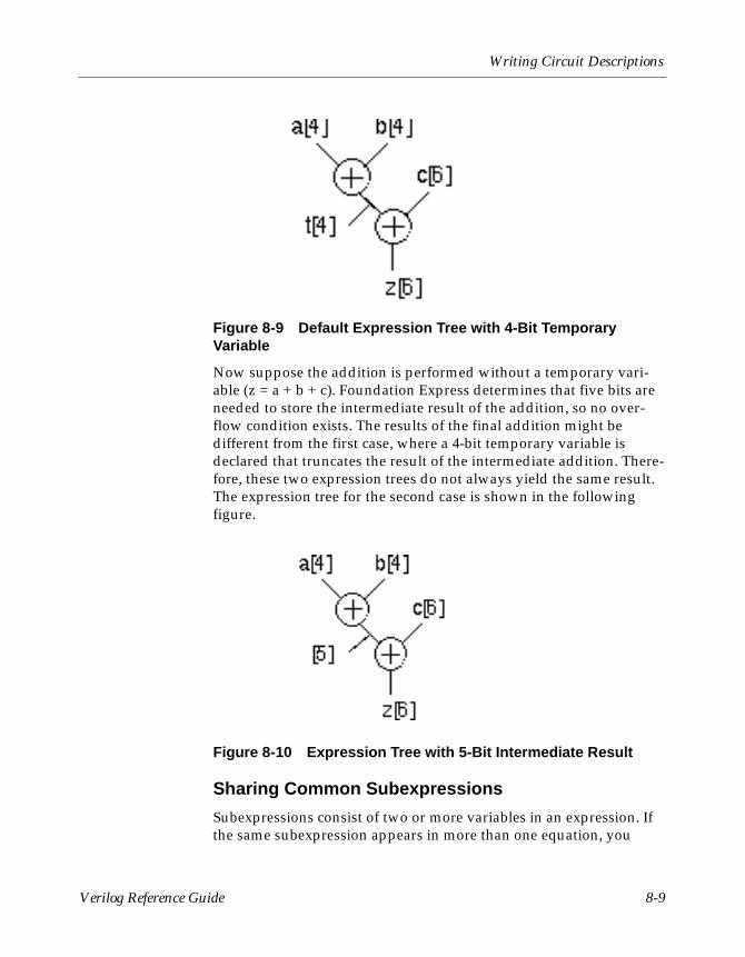
Writing Circuit Descriptions
Figure 8-9 Default Expression Tree with 4-Bit Temporary Variable
Now suppose the addition is performed without a temporary vari-able (z = a + b + c). Foundation Express determines that five bits are needed to store the intermediate result of the addition, so no over-flow condition exists. The results of the final addition might be different from the first case, where a 4-bit temporary variable is declared that truncates the result of the intermediate addition. There-fore, these two expression trees do not always yield the same result. The expression tree for the second case is shown in the following figure.
Figure 8-10 Expression Tree with 5-Bit Intermediate Result
Sharing Common Subexpressions
Subexpressions consist of two or more variables in an expression. If the same subexpression appears in more than one equation, you
Verilog Reference Guide 8-9

Verilog Reference Guide
might want to share these operations to reduce the area of your circuit. You can force common subexpressions to be shared by declaring a temporary variable to store the subexpression, then use the temporary variable wherever you want to repeat the subexpres-sion. The following example shows a group of simple additions that use the common subexpression (a + b).
temp <= a + b;x <= temp;y <= temp + c;
Instead of manually forcing common subexpressions to be shared, you can let Foundation Express automatically determine whether sharing common subexpressions improves your circuit. You do not need to declare a temporary variable to hold the common subexpres-sion in this case.
In some cases, sharing common subexpressions results in more adders being built. Consider the following example, where A + B is a common subexpression.
if cond1Y <= A + B;
elseY <= C + D;
end;if cond2
Z <= E + F;else
Z <= A + B;end;
If the common subexpression A + B is shared, three adders are needed to implement the following section of code.
(A + B)(C + D)(E + F)
If the common subexpression is not shared, only two adders are needed: one to implement the additions A + B and C + D and one to implement the additions E + F and A + B.
Foundation Express analyzes common subexpressions during the resource sharing phase of the compile command and considers area
8-10 Xilinx Development System

Writing Circuit Descriptions
costs and timing characteristics. To turn off the sharing of common subexpressions for the current design, use the constraint manager.
The Foundation Express parser does not identify common subexpres-sions unless you use parentheses or write them in the same order. For example, the two equations in the following example use the common subexpression A + B.
Z <= D + A + B;
The parser does not recognize A + B as a common subexpression, because it parses the second equation as (D + A) + B. You can force the parser to recognize the common subexpression by rewriting the second assignment statement as
Z <= A + B + D;
or
Z <= D + (A + B);
Note: You do not have to rewrite the assignment statement, because Foundation Express recognizes common subexpressions automati-cally.
Using Operator Bit-Width EfficientlyYou can improve circuits by using operators more carefully. In the following example, the adder sums the 8-bit value of a with the lower 4 bits of temp. Although temp is declared as an 8-bit value, the upper 4 bits of temp are always 0, so only the lower 4 bits of temp are needed for the addition.
You can simplify the addition by changing temp to temp [3:0], as shown in the following example. Now, instead of using eight full adders to perform the addition, four full adders are used for the lower 4 bits and four half adders are used for the upper 4 bits. This yields a significant savings in circuit area.
input [7:0] a,b;output [8:0] y;function [8:0] add_lt_10;input [7:0] a,b;reg [7:0] temp;
beginif (b < 10)
temp = b;
Verilog Reference Guide 8-11

Verilog Reference Guide
elsetemp = 10;
add_lt_10 = a + temp [3:0]; // use [3:0] for temp
endendfunctionassign y = add_lt_10(a,b);endmodule
Using State InformationWhen you build finite state machines, you can often specify a constant value of a signal in a particular state. You can write your Verilog description so that Foundation Express produces a more effi-cient circuit.
The following example shows the Verilog description of a simple finite state machine.
module machine (x, clock, current_state, z);
input x, clock;output [1:0] current_state;output z;
reg [1:0] current_state;reg z; /* Redeclared as reg so they can be assigned to in always statements. By default, ports are wires and cannot be assigned to in ’always’ */reg [1:0] next_state;reg previous_z;
parameter [1:0] set0 = 0,hold0 = 1,set1 = 2;
always @ (x or current_state) begin case (current_state)
//synopsys full_case /* declared full_case to avoid extraneous latches
*/set0:
begin
8-12 Xilinx Development System
Writing Circuit Descriptions
z = 0 ; //set z to 0next_state = hold0;end
hold0:beginz = previous_z; //hold value of zif (x == 0)
next_state = hold0;else
next_state = set1;end
set1:beginz = 1; //set z to 1next_state = set0;end
endcaseendalways @ (posedge clock) begin
current_state = next_state;previous_z = z;
endendmodule
In the state hold0, the output z retains its value from the previous state. To synthesize this circuit, a flip-flop is inserted to hold the state previous_z. However, you can make some assertions about the value of z. In the state hold0, the value of z is always 0. This can be deduced from the fact that the state hold0 is entered only from the state set0, where z is always assigned the value 0.
The following example shows how the Verilog description can be changed to use this assertion, resulting in a simpler circuit (because the flip-flop for previous_z is not required). The changed line is shown in bold.
module machine (x, clock, current_state, z);
input x, clock;output [1:0] current_state;output z;
reg [1:0] current_state;reg z;
Verilog Reference Guide 8-13

Verilog Reference Guide
/* Redeclared as reg so they can be assigned to in always statements. By default, ports are wires and cannot be assigned to in ’always’ */reg [1:0] next_state;
parameter [1:0] set0 = 0,hold0 = 1,set1 = 2;
always @ (x or current_state) begincase (current_state) //synopsys full_case /* declared full_case to avoid extraneous latches
*/set0:
beginz = 0 ; //set z to 0next_state = hold0;end
hold0:beginz = 0; //hold z at 0if (x == 0)
next_state = hold0;else
next_state = set1;end
set1:beginz = 1; //set z to 1next_state = set0;end
endcaseendalways @ (posedge clock) begin
current_state = next_state;endendmodule
Describing State MachinesYou can use an implicit state style or an explicit state style to describe a state machine. In the implicit state style, a clock edge (negedge or posedge) signals a transition in the circuit from one state to another.
8-14 Xilinx Development System

Writing Circuit Descriptions
In the explicit state style, you use a constant declaration to assign a value to all states. Each state and its transition to the next state are defined under the case statement. Use the implicit state style to describe a single flow of control through a circuit (where each state in the state machine can be reached only from one other state). Use the explicit state style to describe operations such as synchronous resets.
The following example shows a description of a circuit that sums data over three clock cycles. The circuit has a single flow of control, so the implicit style is preferable.
module sum3 ( data, clk, total );input [7:0] data;input clk;output [7:0] total;
reg total;
alwaysbegin
@ (posedge clk)total = data;
@ (posedge clk)total = total + data;
@ (posedge clk)total = total + data;
endendmodule
Note: With the implicit state style, you must use the same clock phase (either posedge or negedge) for each event expression. Implicit states can be updated only if they are controlled by a single clock phase.
The following example shows a description of the same circuit in the explicit state style. This circuit description requires more lines of code than the previous example, although Foundation Express synthesizes the same circuit for both descriptions.
module sum3 ( data, clk, total );input [7:0] data;input clk;output [7:0] total;
Verilog Reference Guide 8-15

Verilog Reference Guide
reg total;reg [1:0] state;
parameter S0 = 0, S1 = 1, S2 = 2;
always @ (posedge clk)begin
case (state)S0: begin
total = data;state = S1;end
S1: begintotal = total + data;state = S2;end
default : begintotal = total + data;state = S0;end
endcaseendendmodule
The following example shows a description of the same circuit with a synchronous reset added. This example is coded in the explicit state style. Notice that the reset operation is addressed once before the case statement.
module SUM3 ( data, clk, total, reset );input [7:0] data;input clk, reset;output [7:0] total;
reg total;reg [1:0] state;
parameter S0 = 0, S1 = 1, S2 = 2;
always @ (posedge clk)begin
if (reset)state = S0;
8-16 Xilinx Development System

Writing Circuit Descriptions
elsecase (state)S0:begin
total = data;state = S1;
endS1:begin
total = total + data;state = S2;
enddefault : begin
total = total + data;state = S0;
endendcase;
endendmodule
The following example shows how to describe the same function in the implicit state style. This style is not as efficient for describing synchronous resets. In this case, the reset operation has to be addressed for every always @ statement.
module SUM3 ( data, clk, total, reset );input [7:0] data;input clk, reset;output [7:0] total;
reg total;
alwaysbegin: reset_label
@ (posedge clk)if (reset)
begintotal = 8’b0;disable reset_label;
endelse
total = data;
@ (posedge clk)if (reset)
Verilog Reference Guide 8-17

Verilog Reference Guide
begintotal = 8’b0;disable reset_label;
endelse
total = total + data;
@ (posedge clk)if (reset)
begintotal = 8’b0;disable reset_label;
endelse
total = total + data;end
endmodule
Minimizing RegistersIn an always block that is triggered by a clock edge, every variable that has a value assigned has its value held in a flip-flop.
Organize your Verilog description so you build only as many regis-ters as you need. The following example shows a description where extra registers are implied.
module count (clock, reset, and_bits, or_bits, xor_bits);
input clock, reset;output and_bits, or_bits, xor_bits;reg and_bits, or_bits, xor_bits;
reg [2:0] count;
always @(posedge clock) beginif (reset)
count = 3’60;else
count = count + 1;
and_bits = & count;or_bits = | count;xor_bits = ^ count;
8-18 Xilinx Development System

Writing Circuit Descriptions
endendmodule
This description implies the use of six flip-flops: three to hold the values of count and one each to hold and_bits, or_bits, and xor_bits. However, the values of the outputs and_bits, or_bits, and xor_bits depend solely on the values of count. Because count is registered, there is no reason to register the three outputs. The synthesized circuit is shown in the following figure.
Figure 8-11 Synthesized Circuit with Six Implied Registers
To avoid implying extra registers, you can assign the outputs from within an asynchronous always block. The following example shows the same logic described with two always blocks, one synchronous and one asynchronous, which separate registered or sequential logic from combinatorial logic. This technique is useful for describing finite state machines. Signal assignments in the synchronous always block are registered. Signal assignments in the asynchronous always block are not. Therefore, this version of the design uses three fewer flip-flops than the version in the above example.
module count (clock, reset, and_bits, or_bits, xor_bits);
input clock, reset;output and_bits, or_bits, xor_bits;reg and_bits, or_bits, xor_bits;
Verilog Reference Guide 8-19

Verilog Reference Guide
reg [2:0] count;
always @(posedge clock) begin//synchronousif (reset)
count = 3’b0;else
count = count + 1;endalways @(count) begin//asynchronous
and_bits = & count;or_bits = | count;xor_bits = ^ count;
endendmodule
The more efficient version of the circuit is shown in the following figure.
Figure 8-12 Synthesized Circuit with Three Implied Registers
Separating Sequential and Combinatorial Assignments
To compute values synchronously and store them in flip-flops, set up an always block with a signal edge trigger. To let other values change asynchronously, make a separate always block with no signal edge trigger. Put the assignments you want clocked in the always block with the signal edge trigger and the other assignments in the other always block. This technique is used for creating Mealy machines,
8-20 Xilinx Development System

Writing Circuit Descriptions
such as the one in the following example. Note that out changes asyn-chronously with in1 or in2.
module mealy (in1, in2, clk, reset, out);input in1, in2, clk, reset;output out;reg current_state, next_state, out;
always @(posedge clk or negedge reset) // state vector flip-flops (sequential)
if (!reset)current_state = 1’b0;
elsecurrent_state = next_state;
always @(in1 or in2 or current_state)// output and state vector decode (combinatorial)
case (current_state)0: begin
next_state = 1;out = 1’b0;
end1: if (in1) begin
next_state = 1’b0;out = in2;
endelse begin
next_state = 1’b1;out = !in2;
endendcase
endmodule
The schematic for this circuit is shown in the following figure.
Verilog Reference Guide 8-21
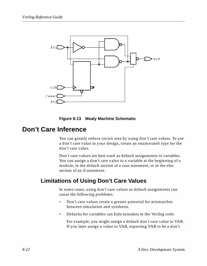
Verilog Reference Guide
Figure 8-13 Mealy Machine Schematic
Don’t Care InferenceYou can greatly reduce circuit area by using don’t care values. To use a don’t care value in your design, create an enumerated type for the don’t care value.
Don’t care values are best used as default assignments to variables. You can assign a don’t care value to a variable at the beginning of a module, in the default section of a case statement, or in the else section of an if statement.
Limitations of Using Don’t Care ValuesIn some cases, using don’t care values as default assignments can cause the following problems.
• Don’t care values create a greater potential for mismatches between simulation and synthesis.
• Defaults for variables can hide mistakes in the Verilog code.
For example, you might assign a default don’t care value to VAR. If you later assign a value to VAR, expecting VAR to be a don’t
8-22 Xilinx Development System

Writing Circuit Descriptions
care value, you might have overlooked an intervening condition under which VAR is assigned.
Therefore, when you assign a value to a variable (or signal) that contains a don’t care value, make sure that the variable (or signal) is really a don’t care value under those conditions. Note that assignment to an x is interpreted as a don’t care value.
Differences Between Simulation and SynthesisDon’t care values are treated differently in simulation and in synthesis, and there can be a mismatch between the two. To a simu-lator, a don’t care is a distinct value, different from a one or a zero. In synthesis, however, a don’t care becomes a zero or a one (and hard-ware is built that treats the don’t care value as either a zero or a one).
Whenever a comparison is made with a variable whose value is don’t care, simulation and synthesis can differ. Therefore, the safest way to use don’t care values is to do the following.
• Assign don’t care values only to output ports
• Make sure that the design never reads output ports
These guidelines guarantee that when you simulate within the scope of the design, the only difference between simulation and synthesis occurs when the simulator indicates that an output is a don’t care value.
If you use don’t care values internally to a design, expressions Foun-dation Express compares to don’t care values (X) are synthesized as though values are not equal to X.
For example,
if A = ’X’ then...
is synthesized as
if FALSE then...
If you use expressions comparing values with X, pre-synthesis and post-synthesis simulation results might not agree. For this reason, Foundation Express issues the following warning.
Verilog Reference Guide 8-23
Verilog Reference Guide
Warning: A partial don’t-care value was read in routine test line 24 in file ’test.v’ This may cause simulation to disagree with synthesis. (HDL-171)
Propagating ConstantsConstant propagation is the compile-time evaluation of expressions that contain constants. Foundation Express uses constant propaga-tion to reduce the amount of hardware required to implement complex operators. Therefore, when you know that a variable is a constant, specify it as a constant. For example, a + operator with a constant of 1 as one of its arguments causes an incrementer, rather than a general adder, to be built. If both arguments of an operator are constants, no hardware is constructed, because Foundation Express can calculate the expression’s value and insert it directly into the circuit.
Comparators and shifters also benefit from constant propagation. When you shift a vector by a constant, the implementation requires only a reordering (rewiring) of bits, so no logic is needed.
Synthesis IssuesThe next two sections describe feedback paths and latches that result from ambiguities in signal or variable assignments and asynchronous behavior.
Feedback Paths and LatchesSometimes your Verilog source can imply combinatorial feedback paths or latches in synthesized logic. This happens when a signal or a variable in a combinatorial logic block (an always block without a posedge or negedge clock statement) is not fully specified. A variable or signal is fully specified when it is assigned under all possible conditions.
Synthesizing Asynchronous DesignsIn a synchronous design, all registers use the same clock signal. That clock signal must be a primary input to the design. A synchronous design has no combinatorial feedback paths, one-shots, or delay lines. Synchronous designs perform the same function regardless of the
8-24 Xilinx Development System

Writing Circuit Descriptions
clock rate, as long as the rate is slow enough to allow signals to prop-agate all the way through the combinatorial logic between registers.
Foundation Express synthesis tools offer limited support for asyn-chronous designs. The most common way to produce asynchronous logic in Verilog is to use gated clocks on registers. If you use asyn-chronous design techniques, synthesis and simulation results might not agree. Because Foundation Express does not issue warning messages for asynchronous designs, you are responsible for verifying the correctness of your circuit.
The following examples show two approaches to the same counter design: The first example is synchronous, and the second example is asynchronous.
module COUNT (RESET, ENABLE, CLK, Z);
input RESET, ENABLE, CLK;output [2:0] Z;reg [2:0] Z;
always @ (posedge CLK) beginif (RESET) begin
Z = 3’b0;end else if (ENABLE == 1’b1) begin
if (Z == 3’d7) beginZ = 3’b0;
end else beginZ = Z + 3’b1;
endend
end
endmodule
The following example shows an asynchronous counter design.
module COUNT (RESET, ENABLE, CLK, Z);
input RESET, ENABLE, CLK;output [2:0] Z;reg [2:0] Z;wire GATED_CLK = CLK & ENABLE;
Verilog Reference Guide 8-25

Verilog Reference Guide
always @ (posedge GATED_CLK or posedge RESET) beginif (RESET) begin
Z = 3’b0;end else begin
if (Z == 3’d7) beginZ = 3’b0;
end else beginZ = Z + 3’b1;
endend
endendmodule
The asynchronous version of the design uses two asynchronous design techniques. The first technique is to enable the counter by ANDing the clock with the enable line. The second technique is to use an asynchronous reset. These techniques work if the proper timing relationships exist between the asynchronous control lines (ENABLE and RESET) and the clock (CLK) and if the control lines are glitch-free.
Some forms of asynchronous behavior are not supported. For example, you might expect the following circuit description of a one-shot signal generator to generate three inverters (an inverting delay line) and a NAND gate.
X = A ~& (~(~(~ A)));
However, this circuit description is optimized to the following.
X = A ~& (~ A); then X = 1;
Designing for Overall EfficiencyThe efficiency of a synthesized design depends primarily on how you describe its component structure. The next two sections explain how to describe random logic and how to share complex operators.
Describing Random LogicYou can describe random logic with many different shorthand Verilog expressions. Foundation Express often generates the same optimized logic for equivalent expressions, so your description style for random logic does not affect the efficiency of the circuit. The following example shows four groups of statements that are equiva-
8-26 Xilinx Development System

Writing Circuit Descriptions
lent. (Assume that a, b, and c are 4-bit variables.) Foundation Express creates the same optimized logic in all four cases.
c = a & b;
c[3:0] = a[3:0] & b[3:0];
c[3] = a[3] & b[3]; c[2] = a[2] & b[2]; c[1] = a[1] & b[1]; c[0] = a[0] & b[0];
for (i = 0; i <= 3; i = i + 1) c[i] = a[i] & b[i];
Sharing Complex OperatorsYou can use automatic resource sharing to share most operators. However, some complex operators can be shared only if you rewrite your source description more efficiently. These operators follow.
• Noncomputable array index
• Function call
• Shifter
The following example shows a circuit description that creates more functional units than necessary when automatic resource sharing is turned off.
module rs(a, i, j, c, y, z);
input [7:0] a;input [2:0] i,j;input c;
output y, z;reg y, z;
always @(a or i or j or c) beginz=0;y=0;if(c)
beginz = a[i];
Verilog Reference Guide 8-27
Verilog Reference Guide
end else
beginy = a[j]; end
endendmodule
The schematic for this code description is shown in the following figure.
8-28 Xilinx Development System

Writing Circuit Descriptions
Figure 8-14 Circuit Schematic with Two Array Indexes
You can rewrite the circuit description in the above example so that it contains only one array index, as shown in the following example.
Verilog Reference Guide 8-29
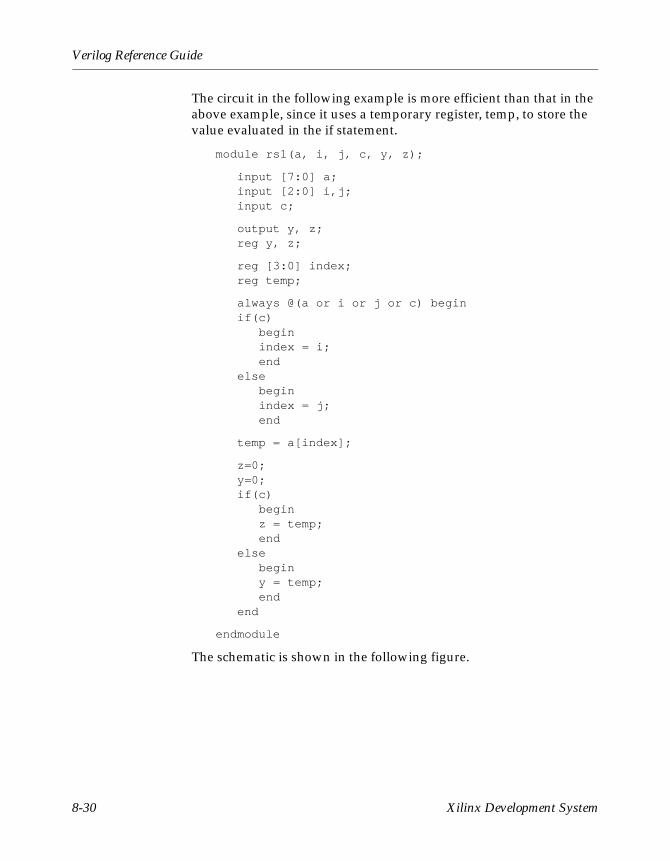
Verilog Reference Guide
The circuit in the following example is more efficient than that in the above example, since it uses a temporary register, temp, to store the value evaluated in the if statement.
module rs1(a, i, j, c, y, z);
input [7:0] a;input [2:0] i,j;input c;
output y, z;reg y, z;
reg [3:0] index;reg temp;
always @(a or i or j or c) beginif(c)
beginindex = i;end
else beginindex = j;end
temp = a[index];
z=0;y=0;if(c)
beginz = temp;end
else beginy = temp;end
end
endmodule
The schematic is shown in the following figure.
8-30 Xilinx Development System

Writing Circuit Descriptions
Figure 8-15 Circuit Schematic with One-Array Index
Consider resource sharing whenever you use a complex operation more than once. Complex operations include adders, multipliers, shifters (only when shifting by a variable amount), comparators, and most user-defined functions.
Verilog Reference Guide 8-31

Verilog Reference Guide
8-32 Xilinx Development System

Chapter 9
Verilog Syntax
This chapter presents the syntax description of the Verilog language supported by Foundation Express and is divided into the following sections.
• “Syntax”
• “Lexical Conventions”
• “Verilog Keywords”
• “Unsupported Verilog Language Constructs”
SyntaxThis section presents the syntax of the supported Verilog language in Backus Naur Form (BNF) and the syntax formalism.
Note: The BNF syntax convention used in this section differs from other syntax convention used elsewhere in this manual.
BNF Syntax FormalismWhite space separates lexical tokens.
name is a keyword.
<name> is a syntax construct definition.
<name> is a syntax construct item.
<name>? is an optional item.
<name>* is zero, one, or more items.
<name>+ is one or more items.
<port> <,<port>>* is a comma-separated list of items.
Verilog Reference Guide 9-1

Verilog Reference Guide
::= gives a syntax definition to an item.
||= refers to an alternative syntax construct.
BNF Syntax<source_text>
::= <description>*
<description> ::= <module>
<module>::= module <name_of_module> <list_of_ports>? ;
<module_item>*endmodule
<name_of_module> ::= <IDENTIFIER>
<list_of_ports> ::= ( <port> <,<port>>* )||= ( )
<port>::= <port_expression>?||= . <name_of_port> ( <port_expression>? )
<port_expression>::= <port_reference>||= { <port_reference> <, <port_reference>>* }
<port_reference>::= <name_of_variable>||= <name_of_variable> [ <expression> ]||= <name_of_variable> [ <expression> :
<expression> ]
<name_of_port>::= <IDENTIFIER>
9-2 Xilinx Development System

Verilog Syntax
<name_of_variable>::= <IDENTIFIER>
<module_item>::= <parameter_declaration>||= <input_declaration>||= <output_declaration>||= <inout_declaration>||= <net_declaration>||= <reg_declaration>||= <integer_declaration>||= <gate_instantiation>||= <module_instantiation>||= <continuous_assign>||= <function>
<function>::= function <range>? <name_of_function> ;
<func_declaration>*<statement_or_null>
endfunction
<name_of_function>::= <IDENTIFIER>
<func_declaration>::= <parameter_declaration>||= <input_declaration>||= <reg_declaration>||= <integer_declaration>
<always>::= always @ ( <identifier> or <identifier> )||= always @ ( posedge <identifier> )||= always @ ( negedge <identifier> )||= always @ ( <egde> or <edge> or ... )
<edge>::= posedge <identifier>||= negedge <identifier>
Verilog Reference Guide 9-3

Verilog Reference Guide
<parameter_declaration>::= parameter <range>? <list_of_assignments> ;
<input_declaration>::= input <range>? <list_of_variables> ;
<output_declaration>::= output <range>? <list_of_variables> ;
<inout_declaration>::= inout <range>? <list_of_variables> ;
<net_declaration>::= <NETTYPE> <charge_strength>? <expandrange>?
<delay>? <list_of_variables> ;||= <NETTYPE><drive_strength>? <expandrange>?
<delay>? <list_of_assignments> ;
<NETTYPE>::= wire||= wor||= wand||= tri
<expandrange>::= <range>||= scalared <range>||= vectored <range>
<reg_declaration>::= reg <range>? <list_of_register_variables> ;
<integer_declaration>::= integer <list_of_integer_variables> ;
<continuous_assign>::= assign <drive_strength>? <delay>?
<list_of_assignments>;
9-4 Xilinx Development System

Verilog Syntax
<list_of_variables>::= <name_of_variable> <, <name_of_variable>>*
<name_of_variable>::= <IDENTIFIER>
<list_of_register_variables>::= <register_variable> <, <register_variable>>*
<register_variable>::= <IDENTIFIER>
<list_of_integer_variables>::= <integer_variable> <, <integer_variable>>*
<integer_variable>::= <IDENTIFIER>
<charge_strength>::= ( small )||= ( medium )||= ( large )
<drive_strength>::= ( <STRENGTH0> , <STRENGTH1> )||= ( <STRENGHT1> , <STRENGTH0> )
<STRENGTH0>::= supply0||= strong0||= pull0||= weak0||= highz0
<STRENGTH1>::= supply1||= strong1||= pull1||= weak1||= highz1
Verilog Reference Guide 9-5

Verilog Reference Guide
<range>::= [ <expression> : <expression> ]
<list_of_assignments>::= <assignment> <, <assignment>>*
<gate_instantiation>::= <GATETYPE> <drive_strength>? <delay>?
<gate_instance> <, <gate_instance>>* ;
<GATETYPE>::= and||= nand||= or||= nor||= xor||= xnor||= buf||= not
<gate_instance>::= <name_of_gate_instance>? ( <terminal> <,
<terminal>>* )
<name_of_gate_instance>::= <IDENTIFIER>
<terminal>::= <identifier>||= <expression>
<module_instantiation>::= <name_of_module>
<parameter_value_assignment>? <module_instance> <,<module_instance>>* ;
<name_of_module>::= <IDENTIFIER>
9-6 Xilinx Development System

Verilog Syntax
<parameter_value_assignment>::= #( <expression> <,<expression>>*)
<module_instance>::= <name_of_module_instance> (
<list_of_module_terminals>? )
<name_of_module_instance>::= <IDENTIFIER>
<list_of_module_terminals>::= <module_terminal>? <,<module_terminal>>*||= <named_port_connection>
<,<named_port_connection>>*
<module_terminal>::= <identifier>||= <expression>
<named_port_connection>::= . IDENTIFIER ( <identifier> )||= . IDENTIFIER ( <expression> )
<statement>::= <assignment>||= if ( <expression> )
<statement_or_null>||= if ( <expression> )
<statement_or_null>else
<statement_or_null>||= case ( <expression> )
<case_item>+endcase
||= casex ( <expression> )<case_item>+
endcase||= casez ( <expression> )
<case_item>+endcase
||= for ( <assignment> ; <expression> ; <assignment> ) <statement>
Verilog Reference Guide 9-7

Verilog Reference Guide
||= <seq_block>||= disable <IDENTIFIER> ;||= forever <statement>||= while ( <expression> ) <statement>
<statement_or_null>::= statement||= ;
<assignment>::= <lvalue> = <expression>
<case_item>::= <expression> <,<expression>>* :
<statement_or_null>||= default : <statement_or_null>||= default <statement_or_null>
<seq_block>::= begin
<statement>*end
||= begin : <name_of_block><block_declaration>*<statement>*
end
<name_of_block>::= <IDENTIFIER>
<block_declaration>::= <parameter_declaration>||= <reg_declaration>||= <integer_declaration>
<lvalue>::= <IDENTIFIER>||= <IDENTIFIER> [ <expression> ]||= <concatenation>
9-8 Xilinx Development System

Verilog Syntax
<expression>::= <primary>||= <UNARY_OPERATOR> <primary>||= <expression> <BINARY_OPERATOR>||= <expression> ? <expression> : <expression>
<UNARY_OPERATOR>::= !||= ~||= &||= ~&||= |||= ~|||= ^||= ~^||= -||= +
<BINARY_OPERATOR>::= +||= -||= *||= /||= %||= ==||= !=||= &&||= ||||= <||= <=||= >||= >=||= &||= |||= <<||= >>
<primary>::= <number>||= <identifier>||= <identifier> [ <expression> ]||= <identifier> [ <expression> : <expression> ]||= <concatenation>||= <multiple_concatenation>
Verilog Reference Guide 9-9
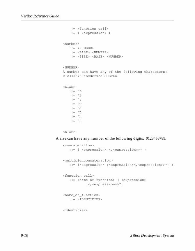
Verilog Reference Guide
||= <function_call>||= ( <expression> )
<number>::= <NUMBER>||= <BASE> <NUMBER>||= <SIZE> <BASE> <NUMBER>
<NUMBER>A number can have any of the following characters: 0123456789abcdefxzABCDEFXZ
<SIZE>::= ’b||= ’B||= ’o||= ’O||= ’d||= ’D||= ’h||= ’H
<SIZE>
A size can have any number of the following digits: 0123456789.
<concatenation>::= { <expression> <,<expression>>* }
<multiple_concatenation>::= {<expression> {<expression><,<expression>>*} }
<function_call>::= <name_of_function> ( <expression>
<,<expression>>*)
<name_of_function>::= <IDENTIFIER>
<identifier>
9-10 Xilinx Development System
Verilog Syntax
An identifier is any sequence of letters, digits, and the underscore character ( _ ), where the first character is a letter or underscore. Upper case and lower case letters are treated as different characters. Identifiers can be any size, and all characters are significant. Escaped identifiers start with the backslash character (\) and end with a space. The leading backslash character (\) is not part of the identifier. Use escaped identifiers to include any printable ASCII characters in an identifier.
<delay>::= # <NUMBER>||= # <identifier>||= # ( <expression> <,<expression>>* )
Lexical ConventionsFoundation Express uses lexical conventions that are nearly identical to those of the Verilog language. The types of lexical tokens that Foundation Express uses are described in the following subsections.
• “White Space”
• “Comments”
• “Numbers”
• “Identifiers”
• “Operators”
• “Macro Substitution”
• “Include Construct”
• “Simulation Directives”
• “Verilog System Functions”
White SpaceWhite space separates words in the input description and can contain spaces, tabs, new lines, and form feeds. You can place white space anywhere in the description. Foundation Express ignores white space.
Verilog Reference Guide 9-11

Verilog Reference Guide
CommentsYou can enter comments anywhere in a Verilog description in two forms.
• Beginning with two backslashes //
Foundation Express ignores all text between these characters and the end of the current line.
• Beginning with the two characters /* and ending with */
Foundation Express ignores all text between these characters, so you can continue comments over more than one line.
Note: You cannot nest comments.
NumbersYou can declare numbers in several different radices and bit-widths. A radix is the base number on which a numbering system is built. For example, the binary numbering system has a radix of 2, octal has a radix of 8, and decimal has a radix of 10.
You can use these three number formats.
• A simple decimal number that is a sequence of digits between 0 and 9
All constants declared in this way are assumed to be 32-bit numbers.
• A number that specifies the bit-width, as well as the radix
These numbers are the same as the previous format, except they are preceded by a decimal number that specifies the bit-width.
• A number followed by a two-character sequence prefix that spec-ifies the number’s size and radix
The radix determines which symbols you can include in the number. Constants declared this way are assumed to be 32-bit numbers. Any of these numbers can include underscores ( _ ). The underscores improve readability and do not affect the value
9-12 Xilinx Development System
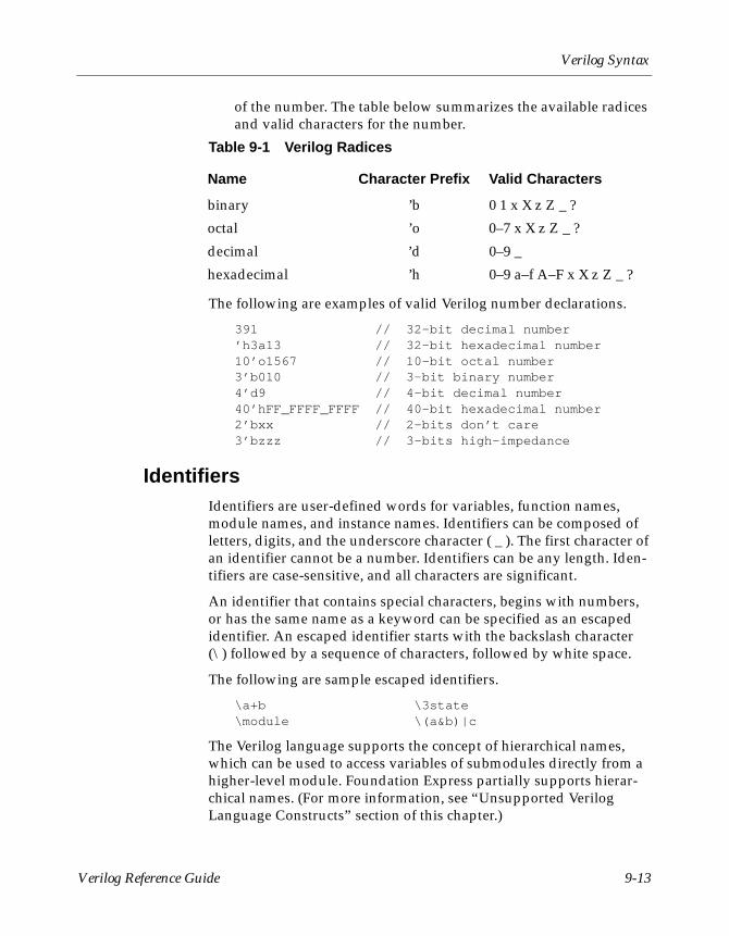
Verilog Syntax
of the number. The table below summarizes the available radices and valid characters for the number.
The following are examples of valid Verilog number declarations.
391 // 32-bit decimal number’h3a13 // 32-bit hexadecimal number10’o1567 // 10-bit octal number3’b010 // 3-bit binary number4’d9 // 4-bit decimal number40’hFF_FFFF_FFFF // 40-bit hexadecimal number2’bxx // 2-bits don’t care3’bzzz // 3-bits high-impedance
IdentifiersIdentifiers are user-defined words for variables, function names, module names, and instance names. Identifiers can be composed of letters, digits, and the underscore character ( _ ). The first character of an identifier cannot be a number. Identifiers can be any length. Iden-tifiers are case-sensitive, and all characters are significant.
An identifier that contains special characters, begins with numbers, or has the same name as a keyword can be specified as an escaped identifier. An escaped identifier starts with the backslash character (\) followed by a sequence of characters, followed by white space.
The following are sample escaped identifiers.
\a+b \3state\module \(a&b)|c
The Verilog language supports the concept of hierarchical names, which can be used to access variables of submodules directly from a higher-level module. Foundation Express partially supports hierar-chical names. (For more information, see “Unsupported Verilog Language Constructs” section of this chapter.)
Table 9-1 Verilog Radices
Name Character Prefix Valid Characters
binary ’b 0 1 x X z Z _ ?
octal ’o 0–7 x X z Z _ ?
decimal ’d 0–9 _
hexadecimal ’h 0–9 a–f A–F x X z Z _ ?
Verilog Reference Guide 9-13

Verilog Reference Guide
OperatorsOperators are one-character or two-character sequences that perform operations on variables. Some examples of operators are +, ~^, <=, and >>. Operators are described in detail in the “Operators” section of the “Expressions” chapter.
Macro SubstitutionMacro substitution assigns a string of text to a macro variable. The string of text is inserted into the code where the macro is encoun-tered. The definition begins with the back quotation mark (‘), followed by the keyword define, followed by the name of the macro variable. All text from the macro variable until the end of the line is assigned to the macro variable.
You can declare and use macro variables anywhere in the descrip-tion. The definitions can carry across several files that are read into Foundation Express at the same time. To make a macro substitution, type a back quotation mark (‘) followed by the macro variable name.
Some sample macro variable declarations are shown in the following example.
‘define highbits 31:29‘define bitlist {first, second, third}wire [31:0] bus;‘bitlist = bus[‘highbits];
Text macros are not supported when used with sized constants, as shown in the following example.
‘define SIZE 4
module test (in,out);output [3:0] out;input [3:0] in;
assign out = ’SIZE’b0101; //text macro from ‘define //statement cannot be used with a sized constant
endmodule
Include ConstructThe include construct in Verilog is similar to the #include directive in C. You can use this construct to include Verilog code, such as type
9-14 Xilinx Development System

Verilog Syntax
declarations and functions, from one module into another module. The following example shows an application of the include construct.
Contents of file1.v
‘define WORDSIZE 8function [WORDSIZE-1:0] fastadder;..endfunction
Contents of secondfile
module secondfile (in1,in2,out)‘include “file1.v”wire [WORDSIZE-1:0] temp;assign temp = fastadder (in1,in2);..endmodule
Included files can include other files, up to 24 levels of nesting. You cannot use the include construct recursively.
Simulation DirectivesSimulation directives refer to special commands that affect the opera-tion of the Verilog HDL Simulator. You can include these directives in your design description, because Foundation Express parses and ignores them.
‘accelerate‘celldefine‘default_nettype‘endcelldefine‘endprotect‘expand_vectornets‘noaccelerate‘noexpand_vectornets‘noremove_netnames‘nounconnected_drive‘protect‘remove_netnames
Verilog Reference Guide 9-15

Verilog Reference Guide
‘resetall‘timescale‘unconnected_drive
Verilog System FunctionsVerilog system functions are implemented by the Verilog HDL simu-lators to generate input or output during simulation. Their names start with a dollar sign ($). Foundation Express parses and ignores Verilog system functions.
9-16 Xilinx Development System

Verilog Syntax
Verilog KeywordsVerilog uses keywords to interpret an input file. You cannot use these words as user variable names unless you use an escaped identifier. For more information, see the “Identifiers” section of this chapter.
always and assign begin
buf bufif0 bufif1 case
casex casez cmos deassign
default defparam disable
end endcase endfunction endmodule
endprimitive endtable endtask event
for force forever fork
function highz0 highz1 if
initial inout input integer
join large medium module
nand negedge nmos nor
not notif0 notif1 or
output parameter pmos posedge
primitive pulldown pullup pull0
pull1 rcmos reg release
repeat rnmos rpmos rtran
rtranif0 rtranif1 scalared small
strong0 strong1 supply0 supply1
table task time
tran tranif0 tranif1 tri
triand trior trireg tri0
tri1 vectored wait wand
weak0 weak1 while wire
wor xnor xor
Verilog Reference Guide 9-17
Verilog Reference Guide
Unsupported Verilog Language ConstructsFoundation Express does not support the following Verilog constructs.
• Unsupported definitions and declarations
• Unsupported statements
• Unsupported operators
• Unsupported gate-level constructs
• Unsupported miscellaneous constructs
Constructs added to the Verilog Simulator in versions after Verilog 1.6 might not be supported.
If you use an unsupported construct in a Verilog description, Foun-dation Express issues a syntax error such as the following.
event is not supported
Unsupported Definitions and DeclarationFoundation Express does not support the following Verilog constructs.
• primitive definition
• time declaration
• event declaration
• triand, trior, tri1, tri0, and trireg net types
• Ranges and arrays for integers
Unsupported StatementsFoundation Express does not support the following Verilog constructs.
• defparam statement
• initial statement
• repeat statement
• delay control
9-18 Xilinx Development System

Verilog Syntax
• event control
• wait statement
• fork statement
• deassign statement
• force statement
• release statement
Unsupported OperatorsFoundation Express does not support the following Verilog constructs.
• Case equality and inequality operators (=== and !==)
• Division and modulus operators for variables
Unsupported Gate-Level ConstructsFoundation Express does not support the following Verilog gate-level constructs.
• nmos
• pmos
• cmos
• rnmos
• rpmos
• rcmos,
• pullup
• pulldown
• tranif0
• tranif1
• rtran
• rtranif0
• rtranif1
Verilog Reference Guide 9-19

Verilog Reference Guide
9-20 Xilinx Development System
Appendix A
Examples
This appendix presents examples that demonstrate basic concepts of Foundation Express.
• “Count Zeros—Combinatorial Version”
• “Count Zeros—Sequential Version”
• “Drink Machine—State Machine Version”
• “Drink Machine—Count Nickels Version”
• “Carry-Lookahead Adder”
Count Zeros—Combinatorial VersionUsing this circuit is one possible solution to a design problem. Given an 8-bit value, the circuit must determine two things:
• The presence of a value containing exactly one sequence of zeros
• The number of zeros in the sequence (if any)
The circuit must complete this computation in a single clock cycle. The input to the circuit is an 8-bit value, and the two outputs the circuit produces are the number of zeros found and an error indica-tion.
A valid value contains only one series of zeros. If more than one series of zeros appears, the value is invalid. A value consisting of all ones is a valid value. If a value is invalid, the count of zeros is set to zero. An example follows,
• The value 00000000 is valid, and the count is eight zeros.
• The value 11000111 is valid, and the count is three zeros.
• The value 00111110 is invalid.
Verilog Reference Guide A-1

Verilog Reference Guide
A Verilog description and a schematic of the circuit are shown in the following example and figure.
module count_zeros(in, out, error); input [7:0] in; output [3:0] out; output error; function legal; input [7:0] x; reg seenZero, seenTrailing; integer i; begin : _legal_block legal = 1; seenZero = 0; seenTrailing = 0; for ( i=0; i <= 7; i=i+1 ) if ( seenTrailing && (x[i] == 1’b0) ) begin legal = 0; disable _legal_block; end else if ( seenZero && (x[i] == 1’b1) ) seenTrailing = 1; else if ( x[i] == 1’b0 ) seenZero = 1; end endfunction
function [3:0] zeros; input [7:0] x; reg [3:0] count; integer i;
begin count = 0; for ( i=0; i <= 7; i=i+1 ) if ( x[i] == 1’b0 ) count = count + 1; zeros = count; end endfunction wire is_legal = legal(in); assign error = ! is_legal; assign out = is_legal ? zeros(in) : 1’b0;endmodule
A-2 Xilinx Development System

Examples
Figure A-1 Count Zeros—Combinatorial Version Block Diagram
This example shows two Verilog functions: legal and zeros. The func-tion legal determines if the value is valid. It returns a 1-bit value: either 1 for a valid value or 0 for an invalid value. The function zeros cycles through all bits of the value, counts the number of zeros, and returns the appropriate value. The two functions are controlled by continuous assignment statements at the bottom of the module defi-nition. This example shows a combinatorial (parallel) approach to counting zeros; the next example shows a sequential (serial) approach.
Count Zeros—Sequential VersionThe following example and figure show a sequential (clocked) solu-tion to the “count zeros” design problem. The circuit specification is slightly different from the specification in the combinatorial solution. The circuit now accepts the 8-bit string serially, 1 bit per clock cycle, using the data and clk inputs. The other two inputs follow.
• reset, which resets the circuit
• read, which causes the circuit to begin accepting data
The circuit’s three outputs follow.
• is_legal, which is true if the data is a valid value
Verilog Reference Guide A-3
Verilog Reference Guide
• data_ready, which is true at the first invalid bit or when all 8 bits have been processed
• zeros, which is the number of zeros if is_legal is true
module count_zeros(data,reset,read,clk,zeros,is_legal, data_ready);
parameter TRUE=1, FALSE=0;
input data, reset, read, clk; output is_legal, data_ready; output [3:0] zeros; reg [3:0] zeros;
reg is_legal, data_ready; reg seenZero, new_seenZero; reg seenTrailing, new_seenTrailing; reg new_is_legal; reg new_data_ready; reg [3:0] new_zeros; reg [2:0] bits_seen, new_bits_seen;
always @ ( data or reset or read or is_legal or data_ready or seenTrailing or seenZero or zeros or bits_seen ) begin if ( reset ) begin new_data_ready = FALSE; new_is_legal = TRUE; new_seenZero = FALSE; new_seenTrailing = FALSE; new_zeros = 0; new_bits_seen = 0; end else begin new_is_legal = is_legal; new_seenZero = seenZero; new_seenTrailing = seenTrailing; new_zeros = zeros; new_bits_seen = bits_seen; new_data_ready = data_ready; if ( read ) begin if ( seenTrailing && (data == 0) ) begin
A-4 Xilinx Development System

Examples
new_is_legal = FALSE; new_zeros = 0; new_data_ready = TRUE; end else if ( seenZero && (data == 1’b1) ) new_seenTrailing = TRUE; else if ( data == 1’b0 ) begin new_seenZero = TRUE; new_zeros = zeros + 1; end
if ( bits_seen == 7 ) new_data_ready = TRUE; else new_bits_seen = bits_seen+1;
endend
end
always @ ( posedge clk) begin zeros = new_zeros; bits_seen = new_bits_seen; seenZero = new_seenZero; seenTrailing = new_seenTrailing; is_legal = new_is_legal; data_ready = new_data_ready;endendmodule
Verilog Reference Guide A-5
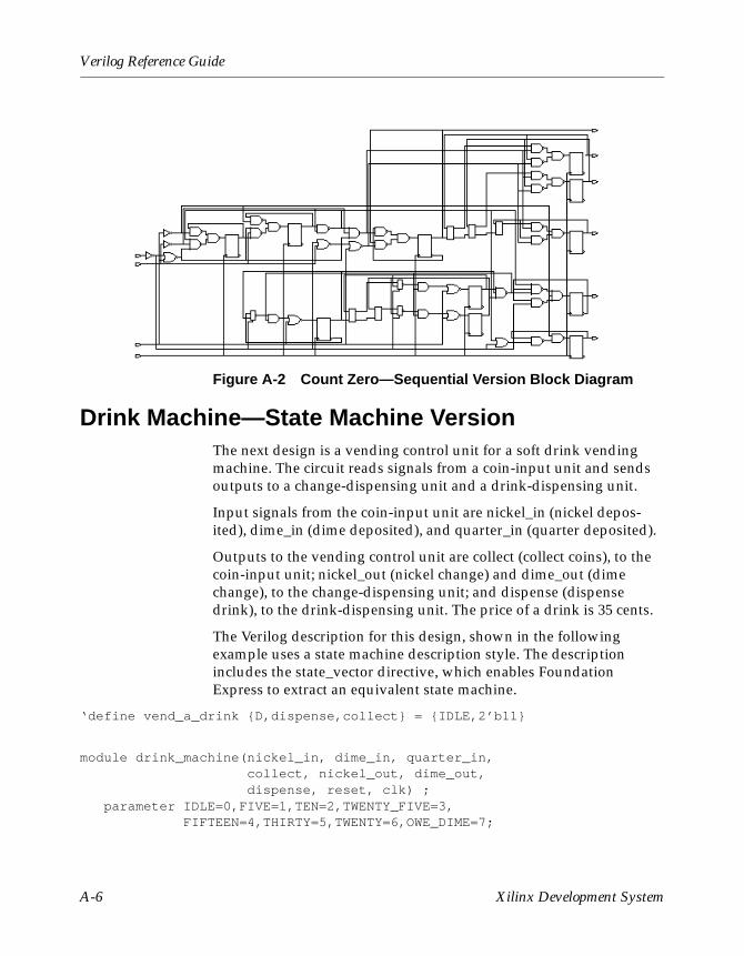
Verilog Reference Guide
Figure A-2 Count Zero—Sequential Version Block Diagram
Drink Machine—State Machine VersionThe next design is a vending control unit for a soft drink vending machine. The circuit reads signals from a coin-input unit and sends outputs to a change-dispensing unit and a drink-dispensing unit.
Input signals from the coin-input unit are nickel_in (nickel depos-ited), dime_in (dime deposited), and quarter_in (quarter deposited).
Outputs to the vending control unit are collect (collect coins), to the coin-input unit; nickel_out (nickel change) and dime_out (dime change), to the change-dispensing unit; and dispense (dispense drink), to the drink-dispensing unit. The price of a drink is 35 cents.
The Verilog description for this design, shown in the following example uses a state machine description style. The description includes the state_vector directive, which enables Foundation Express to extract an equivalent state machine.
‘define vend_a_drink {D,dispense,collect} = {IDLE,2’b11}
module drink_machine(nickel_in, dime_in, quarter_in, collect, nickel_out, dime_out, dispense, reset, clk) ; parameter IDLE=0,FIVE=1,TEN=2,TWENTY_FIVE=3, FIFTEEN=4,THIRTY=5,TWENTY=6,OWE_DIME=7;
A-6 Xilinx Development System
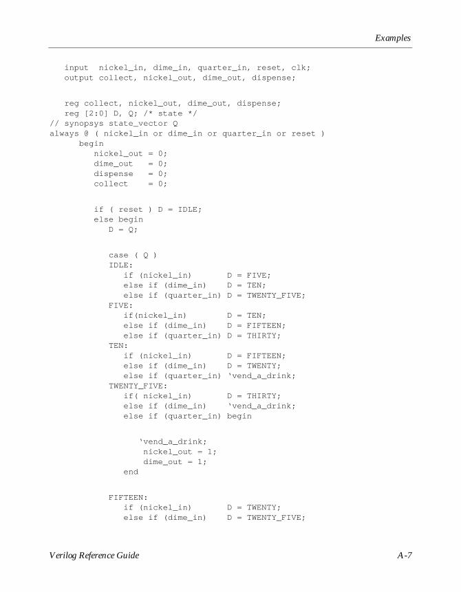
Examples
input nickel_in, dime_in, quarter_in, reset, clk; output collect, nickel_out, dime_out, dispense;
reg collect, nickel_out, dime_out, dispense; reg [2:0] D, Q; /* state */// synopsys state_vector Qalways @ ( nickel_in or dime_in or quarter_in or reset ) begin nickel_out = 0; dime_out = 0; dispense = 0; collect = 0;
if ( reset ) D = IDLE; else begin D = Q;
case ( Q ) IDLE: if (nickel_in) D = FIVE; else if (dime_in) D = TEN; else if (quarter_in) D = TWENTY_FIVE; FIVE: if(nickel_in) D = TEN; else if (dime_in) D = FIFTEEN; else if (quarter_in) D = THIRTY; TEN: if (nickel_in) D = FIFTEEN; else if (dime_in) D = TWENTY; else if (quarter_in) ‘vend_a_drink; TWENTY_FIVE: if( nickel_in) D = THIRTY; else if (dime_in) ‘vend_a_drink; else if (quarter_in) begin
‘vend_a_drink; nickel_out = 1; dime_out = 1; end
FIFTEEN: if (nickel_in) D = TWENTY; else if (dime_in) D = TWENTY_FIVE;
Verilog Reference Guide A-7

Verilog Reference Guide
else if (quarter_in) begin ‘vend_a_drink; nickel_out = 1; end
THIRTY: if (nickel_in) ‘vend_a_drink; else if (dime_in) begin ‘vend_a_drink; nickel_out = 1; end else if (quarter_in) begin ‘vend_a_drink; dime_out = 1; D = OWE_DIME; end
TWENTY: if (nickel_in) D = TWENTY_FIVE; else if (dime_in) D = THIRTY; else if (quarter_in) begin ‘vend_a_drink; dime_out = 1; end
OWE_DIME: begin dime_out = 1; D = IDLE; end endcase endend
always @ (posedge clk ) begin Q = D;endendmodule
A-8 Xilinx Development System

Examples
Figure A-3 Drink Machine—State Machine Version Block Diagram
Drink Machine—Count Nickels VersionThe following example uses the same design parameters as the previous example with the same input and output signals. In this version, a counter counts the number of nickels deposited. This counter is incremented by one if the deposit is a nickel, by two if it’s a dime, and by five if it’s a quarter.
module drink_machine(nickel_in,dime_in,quarter_in,collect, nickel_out,dime_out,dispense,reset,clk);
input nickel_in, dime_in, quarter_in, reset, clk;output nickel_out, dime_out, collect, dispense;
reg nickel_out, dime_out, dispense, collect;reg [3:0] nickel_count, temp_nickel_count;reg temp_return_change, return_change;
always @ ( nickel_in or dime_in or quarter_in or collect or temp_nickel_count or reset or nickel_count or return_change) begin
nickel_out = 0;dime_out = 0;dispense = 0;
Verilog Reference Guide A-9
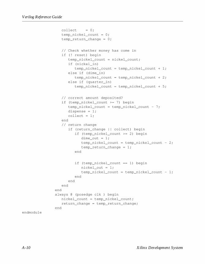
Verilog Reference Guide
collect = 0;temp_nickel_count = 0;temp_return_change = 0;
// Check whether money has come inif (! reset) begin
temp_nickel_count = nickel_count;if (nickel_in)
temp_nickel_count = temp_nickel_count + 1;else if (dime_in)
temp_nickel_count = temp_nickel_count + 2;else if (quarter_in)
temp_nickel_count = temp_nickel_count + 5;
// correct amount deposited?if (temp_nickel_count >= 7) begin
temp_nickel_count = temp_nickel_count - 7;dispense = 1;collect = 1;
end // return change
if (return_change || collect) beginif (temp_nickel_count >= 2) begin
dime_out = 1;temp_nickel_count = temp_nickel_count - 2;temp_return_change = 1;
end
if (temp_nickel_count == 1) beginnickel_out = 1;temp_nickel_count = temp_nickel_count - 1;
endend
endendalways @ (posedge clk ) begin
nickel_count = temp_nickel_count;return_change = temp_return_change;
endendmodule
A-10 Xilinx Development System

Examples
Figure A-4 Drink Machine—Count Nickels Version Block Diagram
Carry-Lookahead AdderThe figure and example in this section show how to build a 32-bit carry-lookahead adder. The adder is built by partitioning of the 32-bit input into eight slices of 4 bits each. The PG module computes propa-gate and generate values for each of the eight slices.
Propagate (output P from PG) is 1 for a bit position if that position propagates a carry from the next-lower position to the next-higher position. Generate (output G) is 1 for a bit position if that position generates a carry to the next-higher position, regardless of the carry-in from the next-lower position.
The carry-lookahead logic reads the carry-in, propagate, and generate information computed from the inputs. It computes the carry value for each bit position. This logic makes the addition opera-tion an XOR of the inputs and the carry values.
The following list shows the order in which the carry values are computed by a three-level tree of 4-bit carry-lookahead blocks (illus-trated in the previous figure):
1. The first level of the tree computes the 32 carry values and the 8 group propagate and generate values. Each of the first-level group propagate and generate values tells if that 4-bit slice prop-
Verilog Reference Guide A-11

Verilog Reference Guide
agates and generates carry values from the next-lower group to the next-higher. The first-level lookahead blocks read the group carry computed at the second level.
2. At the second level of the tree, the lookahead blocks read the group propagate and generate information from the four first-level blocks and then compute their own group propagate and generate information. They also read group carry information computed at the third level to compute the carries for each of the third-level blocks.
3. At the third level of the tree, the third-level block reads the prop-agate and generate information of the second level to compute a propagate and generate value for the entire adder. It also reads the external carry to compute each second-level carry. The carry-out for the adder is 1 if the third-level generate is 1 or if the third-level propagate is 1 and the external carry is 1.
The third-level carry-lookahead block can process four second-level blocks. Because there are only two second-level blocks in the previous figure, the high-order 2 bits of the computed carry are ignored, the high-order 2 bits of the generate input to the third-level are set to 00 (zero), and the propagate high-order bits are set to 11. This causes the unused portion to propagate carries but not to generate them.
The following figure shows the three levels of a block diagram of the 32-bit carry-lookahead adder. The following example shows the code for the adder.
A-12 Xilinx Development System
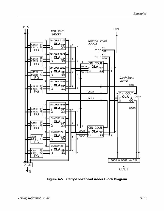
Examples
Figure A-5 Carry-Lookahead Adder Block Diagram
Verilog Reference Guide A-13
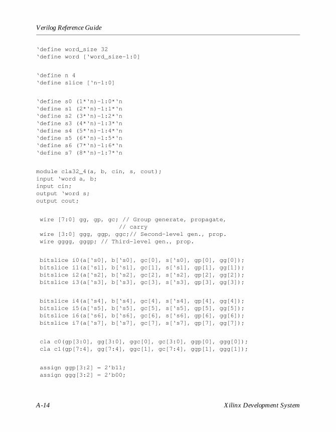
Verilog Reference Guide
‘define word_size 32‘define word [‘word_size-1:0]
‘define n 4‘define slice [‘n-1:0]
‘define s0 (1*‘n)-1:0*‘n‘define s1 (2*‘n)-1:1*‘n‘define s2 (3*‘n)-1:2*‘n‘define s3 (4*‘n)-1:3*‘n‘define s4 (5*‘n)-1:4*‘n‘define s5 (6*‘n)-1:5*‘n‘define s6 (7*‘n)-1:6*‘n‘define s7 (8*‘n)-1:7*‘n
module cla32_4(a, b, cin, s, cout);input ‘word a, b;input cin;output ‘word s;output cout;
wire [7:0] gg, gp, gc; // Group generate, propagate,// carry
wire [3:0] ggg, ggp, ggc;// Second-level gen., prop. wire gggg, gggp; // Third-level gen., prop.
bitslice i0(a[‘s0], b[‘s0], gc[0], s[‘s0], gp[0], gg[0]); bitslice i1(a[‘s1], b[‘s1], gc[1], s[‘s1], gp[1], gg[1]); bitslice i2(a[‘s2], b[‘s2], gc[2], s[‘s2], gp[2], gg[2]); bitslice i3(a[‘s3], b[‘s3], gc[3], s[‘s3], gp[3], gg[3]);
bitslice i4(a[‘s4], b[‘s4], gc[4], s[‘s4], gp[4], gg[4]); bitslice i5(a[‘s5], b[‘s5], gc[5], s[‘s5], gp[5], gg[5]); bitslice i6(a[‘s6], b[‘s6], gc[6], s[‘s6], gp[6], gg[6]); bitslice i7(a[‘s7], b[‘s7], gc[7], s[‘s7], gp[7], gg[7]);
cla c0(gp[3:0], gg[3:0], ggc[0], gc[3:0], ggp[0], ggg[0]); cla c1(gp[7:4], gg[7:4], ggc[1], gc[7:4], ggp[1], ggg[1]);
assign ggp[3:2] = 2’b11; assign ggg[3:2] = 2’b00;
A-14 Xilinx Development System

Examples
cla c2(ggp, ggg, cin, ggc, gggp, gggg); assign cout = gggg | (gggp & cin);endmodule
// Compute sum and group outputs from a, b, cin
module bitslice(a, b, cin, s, gp, gg);input ‘slice a, b;input cin;output ‘slice s;output gp, gg;
wire ‘slice p, g, c; pg i1(a, b, p, g); cla i2(p, g, cin, c, gp, gg); sum i3(a, b, c, s);endmodule
// compute propagate and generate from input bits
module pg(a, b, p, g);input ‘slice a, b;output ‘slice p, g;
assign p = a | b; assign g = a & b;endmodule
// compute sum from the input bits and the carries
module sum(a, b, c, s);input ‘slice a, b, c;output ‘slice s;
wire ‘slice t = a ^ b; assign s = t ^ c;endmodule
// n-bit carry-lookahead block
Verilog Reference Guide A-15

Verilog Reference Guide
module cla(p, g, cin, c, gp, gg);input ‘slice p, g;// propagate and generate bitsinput cin; // carry inoutput ‘slice c; // carry produced for each bitoutput gp, gg; // group generate and group propagate
function [99:0] do_cla; input ‘slice p, g; input cin;
begin : label integer i; reg gp, gg; reg ‘slice c; gp = p[0]; gg = g[0]; c[0] = cin; for(i = 1; i < ‘n; i = i+1) begin gp = gp & p[i]; gg = (gg & p[i]) | g[i]; c[i] = (c[i-1] & p[i-1]) | g[i-1]; end do_cla = {c, gp, gg}; end endfunction
assign {c, gp, gg} = do_cla(p, g, cin);endmodule
A-16 Xilinx Development System